FEATURES
q 25ns maximum (3.3 volt supply) address access time
q MCM contains four (4) 512K x 8 industry-standard
asynchronous SRAMs; the control architecture allows
operation as 8, 16, 24, or 32-bit data width
q TTL compatible inputs and output levels, three-state
bidirectional data bus
q Typical radiation performance
- Total dose: 50krads
- SEL Immune >80 MeV-cm
2
/mg
- LET
TH
(0.25) = >10 MeV-cm
2
/mg
- Saturated Cross Section cm
2
per bit, 5.0E-9
- <1E-8 errors/bit-day, Adams 90% geosynchronous
heavy ion
q Packaging options:
- 68-lead dual cavity ceramic quad flatpack (CQFP) -
(weight 7.37 grams)
q Standard Microcircuit Drawing 5962-01533
- QML T and Q compliant part
INTRODUCTION
The QCOTS
TM
UT8Q512K32 Quantified Commercial
Off-the-Shelf product is a high-performance 2M byte
(16Mbit) CMOS static RAM multi-chip module (MCM),
organized as four individual 524,288 x 8 bit SRAMs with a
common output enable. Memory expansion is provided by
an active LOW chip enable (En), an active LOW output
enable (G), and three-state drivers. This device has a power-
down feature that reduces power consumption by more than
90% when deselected.
Writing to each memory is accomplished by taking the chip
enable (En) input LOW and write enable ( Wn) inputs LOW.
Data on the I/O pins is then written into the location
specified on the address pins (A
0
through A
18
). Reading
from the device is accomplished by taking the chip enable
(En) and output enable (G) LOW while forcing write enable
(Wn) HIGH. Under these conditions, the contents of the
memory location specified by the address pins will appear
on the I/O pins.
The input/output pins are placed in a high impedance state
when the device is deselected (En HIGH), the outputs are
disabled (G HIGH), or during a write operation (En LOW
and Wn LOW). Perform 8, 16, 24 or 32 bit accesses by
making Wn along with En a common input to any
combination of the discrete memory die.
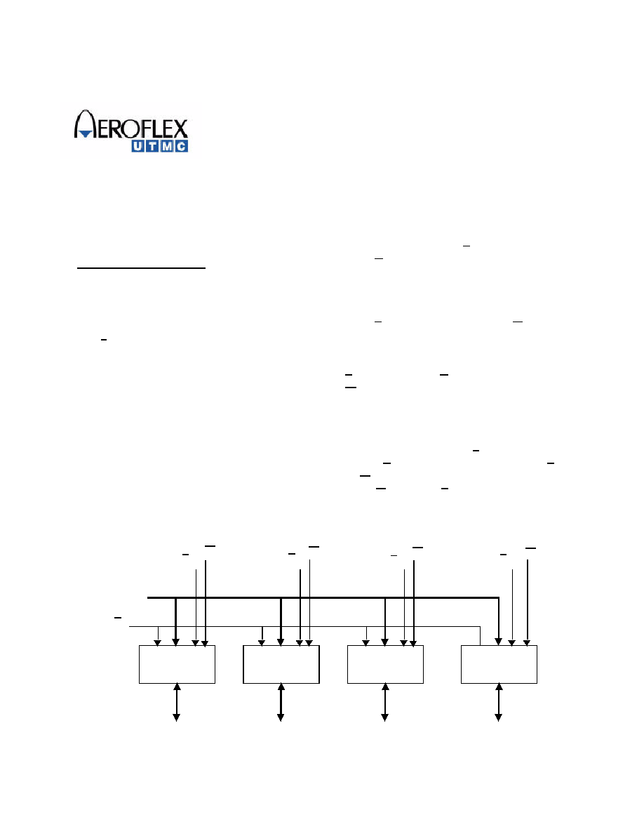
Figure 1. UT8Q512K32 SRAM Block Diagram
512K x 8
512K x 8
512K x 8
512K x 8
DQ(31:24)
or
DQ3(7:0)
DQ(23:16)
or
DQ2(7:0)
DQ(15:3)
or
DQ1(7:0)
DQ(7:0)
or
DQ0(7:0)
G
A(18:0)
W
3
E
3
E
2
E
1
E
0
W
2
W
1
W
0
Standard Products
QCOTS
TM
UT8Q512K32 16Megabit SRAM MCM
Data Sheet
June, 2003
2
PIN NAMES
DEVICE OPERATION
Each die in the UT8Q512K32 has three control inputs called
Enable (En), Write Enable (Wn), and Output Enable (G); 19
address inputs, A(18:0); and eight bidirectional data lines,
DQ(7:0). The device enable (En) controls device selection,
active, and standby modes. Asserting En enables the device,
causes I
DD
to rise to its active value, and decodes the 19 address
inputs to each memory die by selecting the 2,048,000 byte of
memory. Wn controls read and write operations. During a read
cycle, G must be asserted to enable the outputs.
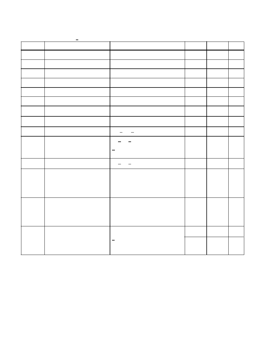
Table 1. Device Operation Truth Table
Notes:
1. "X" is defined as a "don't care" condition.
2. Device active; outputs disabled.
READ CYCLE
A combination of Wn greater than V
IH
(min) with En and G less
than V
IL
(max) defines a read cycle. Read access time is
measured from the latter of device enable, output enable, or valid
address to valid data output.
SRAM read Cycle 1, the Address Access is initiated by a change
in address inputs while the chip is enabled with G asserted and
Wn deasserted. Valid data appears on data outputs DQn(7:0)
after the specified t
AVQV
is satisfied. Outputs remain active
throughout the entire cycle. As long as device enable and output
enable are active, the address inputs may change at a rate equal
to the minimum read cycle time (t
AVAV
).
SRAM read Cycle 2, the Chip Enable-controlled Access is
initiated by En going active while G remains asserted, Wn
remains deasserted, and the addresses remain stable for the
entire cycle. After the specified t
ETQV
is satisfied, the eight-bit
word addressed by A(18:0) is accessed and appears at the data
outputs DQn(7:0).
SRAM read Cycle 3, the Output Enable-controlled Access is
initiated by G going active while En is asserted, Wn is
deasserted, and the addresses are stable. Read access time is
t
GLQV
unless t
AVQV
or t
ETQV
have not been satisfied.
A(18:0)
Address
Wn
WriteEnable
DQ(7:0)
Data Input/Output
G
Output Enable
En
Device Enable
V
DD
Power
V
SS
Ground
10
11
12
13
14
15
16
17
18
19
20
21
22
23
24
25
26
60
59
58
57
56
55
54
53
52
51
50
49
48
47
46
45
44
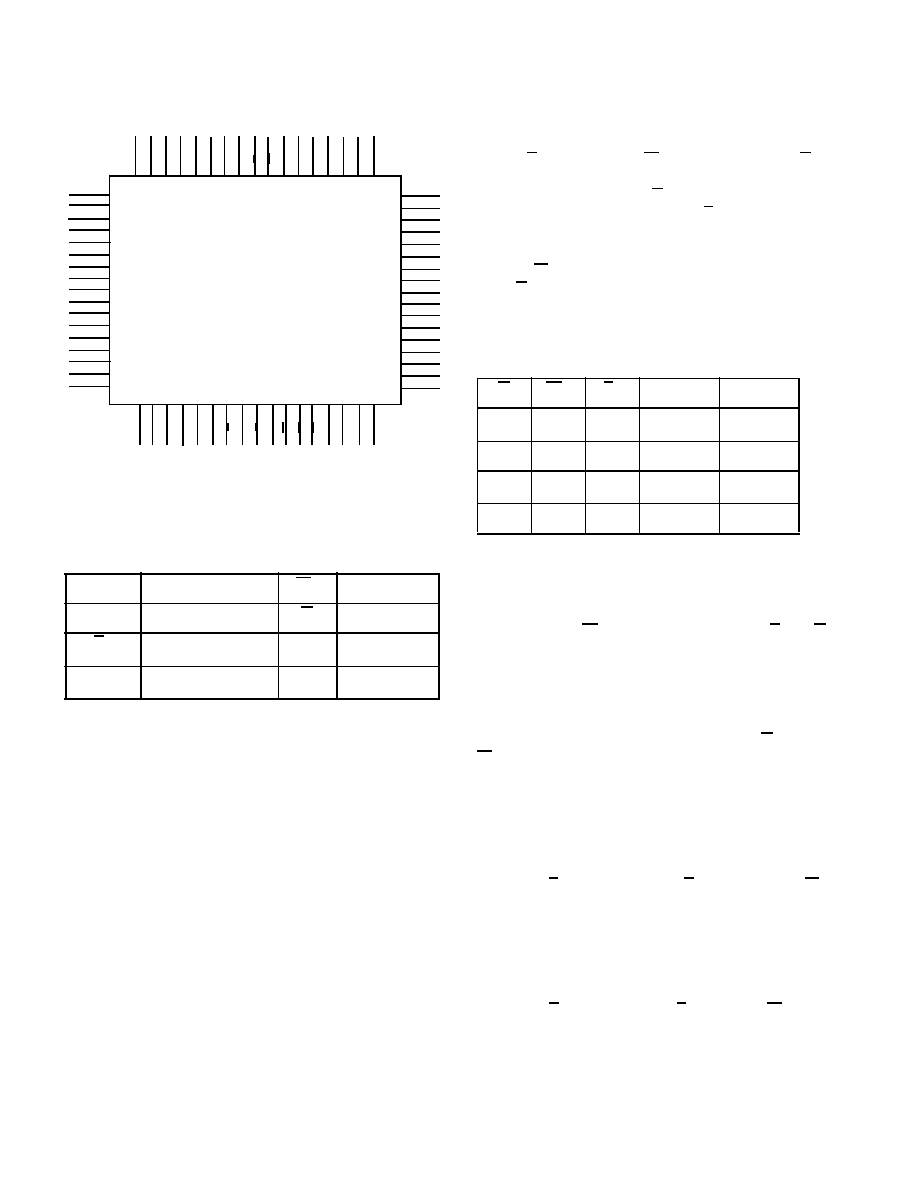
9 8 7 6 5 4 3 2 1 68 67 66 65 64 63 62 61
27 28 29 30 31 32 33 34 35 36 37 38 39 40 41 42 43
Top View
DQ0(0)
DQ1(0)
DQ2(0)
DQ3(0)
DQ4(0)
DQ5(0)
DQ6(0)
DQ7(0)
V
SS
DQ0(1)
DQ1(1)
DQ2(1)
DQ3(1)
DQ4(1)
DQ5(1)
DQ6(1)
DQ7(1)
DQ0(2)
DQ1(2)
DQ2(2)
DQ3(2)
DQ4(2)
DQ5(2)
DQ6(2)
DQ7(2)
V
SS
DQ0(3)
DQ1(3)
DQ2(3)
DQ3(3)
DQ4(3)
DQ5(3)
DQ6(3)
DQ7(3)
N
C
A
0
A
1
A
2
A
3
A
4
A
5
E
2
V
S
S
E
3
W
0
A
6
A
7
A
8
A
9
A
1
0
V
D
D
V
D
D
A
1
1
A
1
2
A
1
3
A
1
4
A
1
5
A
1
6
E
0
G
E
1
A
1
7
W
1
W
2
W
3
A
1
8
N
C
N
C
Figure 2. 25ns SRAM Pinout (68)
G
Wn
En
I/O Mode
Mode
X
1
X
1
3-state
Standby
X
0
0
Data in
Write
1
1
0
3-state
Read
2
0
1
0
Data out
Read
3
WRITE CYCLE
A combination of Wn less than V
IL
(max) and En less than
V
IL
(max) defines a write cycle. The state of G is a "don't care"
for a write cycle. The outputs are placed in the high-impedance
state when either G is greater than V
IH
(min), or when Wn is less
than V
IL
(max).
Write Cycle 1, the Write Enable-controlled Access is defined
by a write terminated by Wn going high, with En still active.
The write pulse width is defined by t
WLWH
when the write is
initiated by Wn, and by t
ETWH
when the write is initiated by En.
Unless the outputs have been previously placed in the high-
impedance state by G, the user must wait t
WLQZ
before applying
data to the eight bidirectional pins DQn(7:0) to avoid bus
contention.
Write Cycle 2, the Chip Enable-controlled Access is defined by
a write terminated by the former of En or Wn going inactive.
The write pulse width is defined by t
WLEF
when the write is
initiated by Wn, and by t
ETEF
when the write is initiated by the
En going active. For the Wn initiated write, unless the outputs
have been previously placed in the high-impedance state by G,
the user must wait t
WLQZ
before applying data to the eight
bidirectional pins DQn(7:0) to avoid bus contention.
TYPICAL RADIATION HARDNESS
The UT8Q512K32 SRAM incorporates features which allow
operation in a limited radiation environment.
Table 2. Typical Radiation Hardness
Design Specifications
1
Notes:
1. The SRAM will not latchup during radiation exposure under recommended
operating conditions.
2. 90% worst case particle environment, Geosynchronous orbit, 100 mils of
Aluminum.
Total Dose
50
krad(Si) nominal
Heavy Ion
Error Rate
2
<1E-8
Errors/Bit-Day
4
ABSOLUTE MAXIMUM RATINGS
1
(Referenced to V
SS
)
Notes:
1. Stresses outside the listed absolute maximum ratings may cause permanent damage to the device. This is a stress rating only, and functional operation of the device
at these or any other conditions beyond limits indicated in the operational sections of this specification is not recommended. Exposure to absolute maximum rating
conditions for extended periods may affect device reliability and performance.
2. Maximum junction temperature may be increased to +175
∞
C during burn-in and steady-static life.
3. Test per MIL-STD-883, Method 1012.
RECOMMENDED OPERATING CONDITIONS
SYMBOL
PARAMETER
LIMITS
V
DD
DC supply voltage
-0.5 to 4.6V
V
I/O
Voltage on any pin
-0.5 to 4.6V
T
STG
Storage temperature
-65 to +150
∞
C
P
D
Maximum power dissipation
1.0W (per byte)
T
J
Maximum junction temperature
2
+150
∞
C
JC
Thermal resistance, junction-to-case
3
10
∞
C/W
I
I
DC input current
±
10 mA
SYMBOL
PARAMETER
LIMITS
V
DD
Positive supply voltage
3.0 to 3.6V
T
C
Case temperature range
-40 to +125
∞
C
V
IN
DC input voltage
0V to V
DD
5
DC ELECTRICAL CHARACTERISTICS (Pre/Post-Radiation)*
(-40
∞
C to +125
∞
C) (V
DD
= 3.3V + 0.3)
Notes:
* Post-radiation performance guaranteed at 25
∞
C per MIL-STD-883 Method 101 9 .
1. Measured only for initial qualification and after process or design changes that could affect input/output capacitance.
2. Supplied as a design limit but not guaranteed or tested.
3. Not more than one output may be shorted at a time for maximum duration of one second.
SYMBOL
PARAMETER
CONDITION
MIN
MAX
UNIT
V
IH
High-level input voltage
(CMOS)
2.0
V
V
IL
Low-level input voltage
(CMOS)
0.8
V
V
OL1
Low-level output voltage
I
OL
= 8mA, V
DD
=3.0V
0.4
V
V
OL2
Low-level output voltage
I
OL
= 200
µ
A,V
DD
=3.0V
0.08
V
V
OH1
High-level output voltage
I
OH
= -4mA,V
DD
=3.0V
2.4
V
V
OH2
High-level output voltage
I
OH
= -200
µ
A,V
DD
=3.0V
V
DD
-0.10
V
C
IN
1
Input capacitance
= 1MHz @ 0V
32
pF
C
IO
1
Bidirectional I/O capacitance
= 1MHz @ 0V
16
pF
I
IN
Input leakage current
V
SS
< V
IN
< V
DD,
V
DD
= V
DD
(max)
-2
2
µ
A
I
OZ
Three-state output leakage current
0V < V
O
< V
DD
V
DD
= V
DD
(max)
G = V
DD
(max)
-2
2
µ
A
I
OS
2, 3
Short-circuit output current
0V < V
O
< V
DD
-90
90
mA
I
DD
(OP)
Supply current operating
@ 1MHz
(per byte)
Inputs: V
IL
= 0.8V,
V
IH
= 2.0V
I
OUT
= 0mA
V
DD
= V
DD
(max)
125
mA
I
DD1
(OP)
Supply current operating
@40MHz
(per byte)
Inputs: V
IL
= 0.8V,
V
IH
= 2.0V
I
OUT
= 0mA
V
DD
= V
DD
(max)
180
mA
I
DD2
(SB)
Nominal standby supply current
@0MHz
(per byte)
Inputs: V
IL
= V
SS
I
OUT
= 0mA
En = V
DD
- 0.5,
V
DD
= V
DD
(max)
V
IH
= V
DD
- 0.5V
6
40
mA
mA
-40
∞
C and
25
∞
C
+125
∞
C