 | –≠–ª–µ–∫—Ç—Ä–æ–Ω–Ω—ã–π –∫–æ–º–ø–æ–Ω–µ–Ω—Ç: 131L | –°–∫–∞—á–∞—Ç—å:  PDF PDF  ZIP ZIP |

Data Sheet
November 2000
131-Type Long-Wavelength PIN Photodetector
The 131-Type PIN low-profile photodetector offers excellent
coupling stability based on Lucent Technologies
Microelectronics Group's patented Advanced Lightwave
Platform technology.
Features
s
Wavelength: 1.1
µ
m--1.6
µ
m
s
Planar structure for high reliability
s
Low-profile, 8-lead DIP package
s
Wide operating temperature range:
≠40
∞
C to +85
∞
C
s
High optical coupling stability
s
Wide selection of fiber pigtails and connectors
available
s
High performance:
-- High responsivity
-- Very low dark current
-- High optical input saturation level
-- High speed for digital applications
-- High linearity and low back reflections for ana-
log applications
Applications
Digital
s
Telecommunications:
-- Fiber-in-the-loop (FITL) narrowband application
-- SONET/SDH transmission systems
-- Digital cellular
s
Datacom:
-- Local area networks
-- 1 Gbit/s fibre channel
s
Military:
-- Microwave systems
-- Remote antennae
-- Tactical communications
Analog
s
Analog systems:
-- CATV trunk and loop
-- Micro-/picocellular
-- Microwave
s
Telecommunications:
-- Fiber in the loop (FITL)
-- Broadband
s
Military:
-- Microwave systems
-- Remote antennae
-- Tactical communications
2
2
Lucent Technologies Inc.
Data Sheet
November 2000
131-Type Long-Wavelength PIN Photodetector
Description
The 131-Type photodetectors represent a family of low-
profile, high-reliability pigtailed devices specially
engineered for the rigorous demands of either analog
applications or digital fiber-optic applications. These
photodetectors are based upon Lucent Technologies'
patented Advanced Lightwave Platform technology,
permitting high optical coupling stability and
unparalleled performance.
The low-profile package is an 8-lead DIP that allows
pinout-equivalent replacements for lower-performance
coaxial-type packages. The low profile makes it ideal
for close board-to-board spacing situations.
The 131-Type PIN Photodetectors contain a rear-
illuminated planar diode structure. Lucent Technologies
employs unique diode processing steps to achieve a
low capacitance and highly linear active area that
ensures a wide dynamic operating range. Responsivity
is typically >0.85 A/W with rise and fall times of <0.5 ns
at the 1.3
µ
m wavelength.
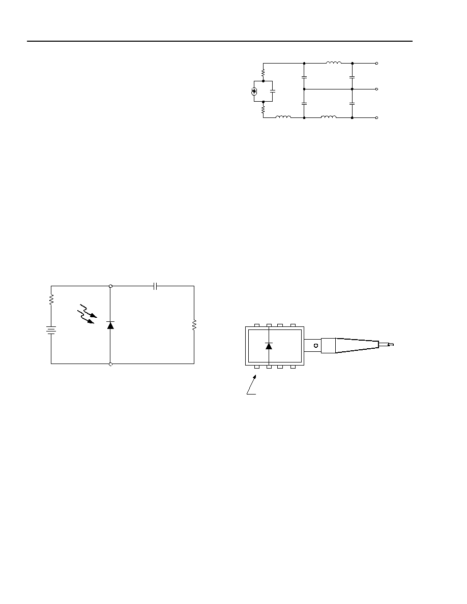
Figure 1. Typical Bias Connection
This PIN's construction involves a patented silicon
optical bench that supplies mechanical stability to the
fiber and directive channeling of input light. The
structure also allows it to handle strong levels of input
power. All fiber types are specially terminated inside
the package to minimize back reflections.
These PIN photodetectors perform effectively and
efficiently over the entire 1.1
µ
m to 1.6
µ
m long
wavelength range. They have been employed in a
number of diverse applications including digital cellular,
remote monitoring, high-speed datacom, fiber-to-the-
curb, and CATV signaling.
Notes:
This equivalent circuit is intended as an aid for modeling the device/
package parasitics in order for the circuit designer to better match
impedance and optimize bandwidth performance.
Minimum parasitic effects can be achieved by connecting the PIN
cathode (N-side) to circuit ground, applying a negative voltage to the
PIN anode (P-side), and allowing the package voltage to float by
not
connecting the package ground to circuit ground.
Typical values are as follows:
C
O
= Bulk capacitance of the diode = 0.3 pF to 0.5 pF.
R
NSS
, R
PSS
= Bulk resistance of the contacts = 5
.
L
SBW
= Series inductance of P-side bond wire = 0.25 nH.
C
NSS
, C
PSS
= Substrate capacitance = 0.975 pF/0.28 pF, respectively.
L
NBW
, L
PBW
= Series inductance of the substrate to package lead
bond wire = 2.0 nH.
C
NPL
, C
PPL
= Package lead capacitance = 0.40 pF/0.46 pF,
respectively.
Figure 2. Equivalent ac Circuit for Analog
Applications
Figure 3. 8-Lead DIP Electrical Connections
1-928
R
BIAS
V
BIAS
+
(N-SIDE)
PIN CATHODE
R
LOAD
PIN ANODE
(P-SIDE)
CAPACITOR
dc DECOUPLING
1-929
R
NSS
R
PSS
(P-SIDE)
PIN ANODE
L
NBW
L
PBW
C
NSS
C
PSS
C
NPL
C
PPL
PACKAGE
GROUND
(N-SIDE)
PIN CATHODE
L
SBW
C
O
PIN
CURRENT
SOURCE
1-698
4 3 2 1
5 6 7 8
GROUND (OPTIONAL)
TERMINAL N
TERMINAL P

Lucent Technologies Inc.
3
Data Sheet
November 2000
131-Type Long-Wavelength PIN Photodetector
Absolute Maximum Ratings
Stresses in excess of the absolute maximum ratings can cause permanent damage to the device. These are
absolute stress ratings only. Functional operation of the device is not implied at these or any other conditions in
excess of those given in the operational sections of the data sheet. Exposure to absolute maximum ratings for
extended periods can adversely affect device reliability.
* The recommended reverse bias voltage is 5 V to 15 V.
Handling Precautions
Electrostatic Discharge
CAUTION: This device is susceptible to damage as a result of electrostatic discharge. Take proper
precautions during both handling and testing. Follow guidelines such as JEDEC Publication No.
108-A (Dec. 1988).
Although protection circuitry is designed into the device, take proper precautions to avoid exposure to ESD.
Lucent Technologies employs a human-body model (HBM) for ESD-susceptibility testing and protection-design
evaluation. ESD voltage thresholds are dependent on the critical parameters used to define the model. A standard
HBM (resistance = 1.5 k
, capacitance = 100 pF) is widely used and, therefore, can be used for comparison
purposes. The HBM ESD threshold presented here was obtained by using the following circuit parameters:
Parameter
Symbol
Min
Max
Unit
Operating Temperature Range
T
A
≠40
85
∞
C
Storage Temperature Range
T
stg
≠40
90
∞
C
Forward Voltage
V
F
--
0
V
Reverse Voltage*
V
R
--
30
V
Photocurrent
--
--
4
mA
Humidity
--
--
95
%
ESD Threshold
--
--
>250
V
Parameter
Value
Unit
HBM Threshold
250
V

4
Lucent Technologies Inc.
Data Sheet
November 2000
131-Type Long-Wavelength PIN Photodetector
Electrical Characteristics
Minimum and maximum values are testing requirements. Typical values are for informational purposes only and are
not part of the testing requirements. Each device is provided with recommended operating conditions to achieve
specified performance. T
C
= 25
∞
C, unless noted otherwise. Determinations made using a 50
load.
* The minimum capacitance configuration occurs when the N-side of the PIN is grounded and a negative voltage is applied to the P-side, with
the package floating, not grounded (value reference only; not tested in manufacture).
Optical Characteristics
T
C
= 25
∞
C.
* Does not include rotary mechanical splice loss (index matching is recommended).
Second-order linearity measured at 15 V bias. The two tones are chosen to lie in the interval f
1
> 50 MHz, f
2
< 200 MHz; or such that f
1
+ f
2
=
860 MHz and f
1
≠ f
2
= 50 MHz. See Figure 7 for typical bias response.
Third-order linearity measured at 8 V bias. The two tones chosen are f
1
= 135.0 MHz and f
2
= 189.25 MHz. See Figure 8 for typical bias
response.
Parameter
Symbol
Min
Typ
Max
Unit
Capacitance (f < 900 MHz):
131 8-Lead DIP*
--
--
0.7
--
pF
Rise/Fall Time
t
R/
t
F
--
<0.5
--
ns
Dark Current
I
D
--
1.0
5
nA
Reverse Voltage
V
R
2
15
30
V
Parameter
Symbol
Min
Typ
Max
Unit
Responsivity:
Type 1
Type 2
Type 3
R
R
R
0.75
0.85
0.90
0.85
0.92
0.95
--
--
--
A/W
A/W
A/W
Optical Back Reflection*:
Type 1
Type 2
--
--
--
--
≠35
≠60
≠20
≠40
dB
dB
Wavelength Range
--
1.1
--
1.6
µ
m
Linearity:
Type L1:
Second Order
Third Order
Type L2:
Second Order
Third Order
Type L3:
Second Order
Third Order
Type L4:
Second Order
Third Order
Type L5:
Second Order
Third Order
--
--
--
--
--
--
--
--
--
--
--
--
--
--
--
--
--
--
--
--
≠52
≠65
≠68
≠70
≠75
≠75
≠80
--
≠85
≠85
≠48
≠60
≠63
≠65
≠70
≠70
≠75
≠80
≠80
≠80
dBc
dBc
dBc
dBc
dBc
dBc
dBc
dBc
dBc
dBc
Lucent Technologies Inc.
5
Data Sheet
November 2000
131-Type Long-Wavelength PIN Photodetector
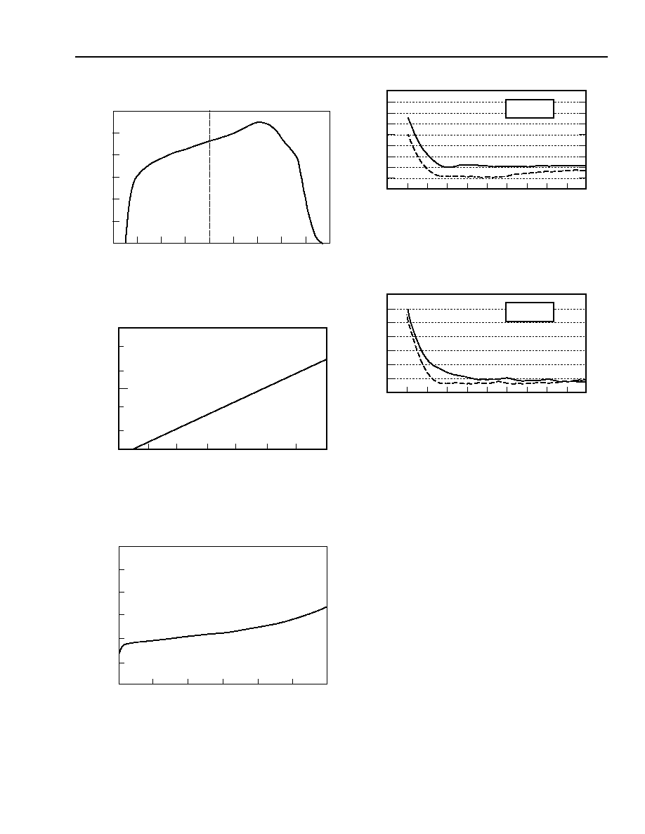
Characteristic Curves
Figure 4. Responsivity as a Function of Wavelength
Figure 5. Typical Temperature Dependence of Dark
Current
Figure 6. Reverse I-V at 23
∞
C
Figure 7. Second-Order Linearity, 1310 nm
Wavelength; 0 dBm Optical Received
Power; Two Tones @ 35% OMD per Tone
Figure 8. Third-Order Linearity, 1310 nm
Wavelength; 0 dBm Optical Received
Power; Two Tones @ 35% OMD per Tone
1-072
WAVELENGTH (µm)
RESPONSIVITY (A/W)
1.1
1.3
1.5
1.7
0.2
0.6
1.0
0.4
0.8
0.0
1-381
10
≠7
70
30
40
60
50
10
≠8
10
≠9
20
80
90
Id (A) (@ ≠10 V
BIAS
)
TEMPERATURE (
∞
C)
1-380
10
30
40
60
0
20
50
10
≠5
10
≠6
10
≠8
10
≠9
REVERSE VOLTAGE (V)
Id (A)
10
≠7
10
≠10
10
≠11
1-926
-- f
1
+ f
2
--- f
2
≠ f
1
dBc
BIAS VOLTAGE
≠20
≠40
≠60
≠80
≠100
≠10
≠30
≠50
≠70
≠90
2
4
6
8
10
12
14
16
18
0
20
1-927
-- 2f
2
≠ f
1
--- 2f
1
+ f
2
dBc
BIAS VOLTAGE
≠40
≠60
≠80
≠100
≠30
≠50
≠70
≠90
2
4
6
8
10
12
14
16
18
0
20