 | –≠–ª–µ–∫—Ç—Ä–æ–Ω–Ω—ã–π –∫–æ–º–ø–æ–Ω–µ–Ω—Ç: 1345TMPC | –°–∫–∞—á–∞—Ç—å:  PDF PDF  ZIP ZIP |
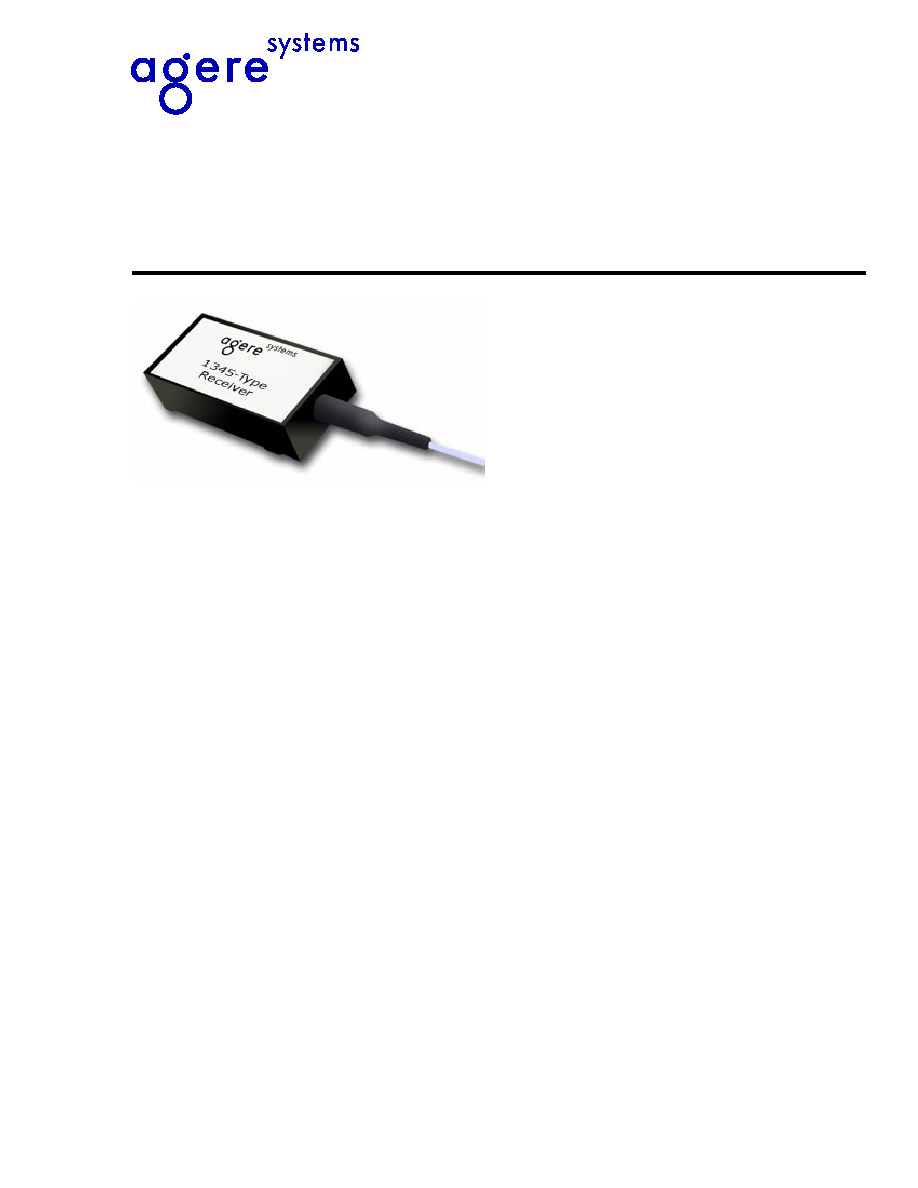
1345-Type Receiver with
Clock Recovery and Data Retiming
Data Sheet
January 2000
Operating at 1.3
µ
m or 1.55
µ
m wavelengths and at
155 Mbits/s or 622 Mbits/s, the versatile 1345-Type Receiver is
manufactured in a 20-pin, plastic DIP with a multimode fiber
pigtail.
Features
s
Backward compatible with 1330 family
s
Space-saving, self-contained, 20-pin plastic DIP
s
Silicon based ICs
s
Single 5 V power supply operation including
photocurrent monitor capability
s
Exceeds all SONET (GR-253-CORE) and ITU-T
G.958 jitter requirements
s
Clocked decision circuit
s
Regenerated differential clock signal
s
Wide dynamic range
s
Qualified to meet the intent of
Telcordia Technolo-
gies
TM reliability practices
s
Operates at data rates of 155 Mbits/s or
622 Mbits/s
s
Positive ECL (PECL) data outputs
s
CMOS (TTL) link-status flag output
s
Operation at 1.3
µ
m or 1.55
µ
m wavelengths
s
Operating temperature range of ≠40 ∞C to +85 ∞C
Applications
s
Telecommunications:
-- Inter- and intraoffice SONET/ITU-T SDH
-- Subscriber loop
-- Metropolitan area networks
s
High-speed data communications
Description
The 1345-Type fiber-optic receiver is designed for
use in transmission systems or medium- to high-
speed data communication applications. Used in
intermediate- and long-reach applications, the
receiver operates at the SONET OC-3 or OC-12 data
rate as well as the ITU-T synchronous digital hierar-
chy (SDH) rate of STM-1 or STM-4, depending on
the receiver model chosen. The receiver meets all
present
Telcordia Technologies
GR-253-CORE
requirements, the current ANSI T1X1.5 intraoffice
specifications, and the ITU-T G.957 and G.958 rec-
ommendations. Compact packaging, a high level of
integration, and a wide dynamic range make these
receivers ideal for data communications.
Manufactured in a 20-pin DIP, the receiver consists of
a planar InGaAs PIN photodetector, a silicon pream-
plifier, a silicon bipolar limiting amplifier that converts
the small signal to ECL levels, a timing recovery unit
to recover the clock, and a silicon bipolar decision cir-
cuit.

2
2
Agere Systems Inc.
1345-Type Receiver with
Data Sheet
Clock Recovery and Data Retiming
January 2000
Description
(continued)
The receiver converts optical signals in the range of
1.1
µ
m to 1.6
µ
m into retimed clock and data signals.
The clock and data outputs are raised-ECL (PECL)
logic levels. A CMOS-level flag output indicates when
there is a loss of optical signal.
The receiver requires a 5 V power supply for the ampli-
fier, logic, and PLL CRC circuits. The operating case
temperature range is ≠40 ∞C to +85 ∞C.
Pin 10
Pin 10 on the 1345-Type receiver is not an internally
connected (NIC) pin. This definition allows the 1345 to
be used in most customer 20-pin receiver module
applications. Customer's printed-wiring boards that are
designed with ground, +5 V, ≠5 V, or no connection to
this pin are all acceptable options. For those applica-
tions that require monitoring the photocurrent of the
PIN photodetector for power monitoring purposes,
there are versions of the 1345 that require +5 V or ≠5 V
applied to Pin 10. Check Tables 3 and 4 for ordering
information.
Flag Output
When the optical input falls below the link status flag
switching threshold, the link status flag is deactivated
and its output logic level changes from a CMOS logic
HIGH to a CMOS logic LOW.
Squelched Data and Clock Outputs
In some versions of the 1345 receiver (see Table 4),
when the link status flag is deactivated, the data and
clock outputs are squelched (stop outputting a signal).
When this occurs, the DATA, DATA, CLOCK, and
CLOCK
outputs switch to a constant dc output voltage
level of 1.3 V.
Nonsquelched Data and Clock Outputs
Agere Systems also manufactures nonsquelching ver-
sions of the 1345 receiver for those applications that
require the data and clock outputs to continue to func-
tion after the link status flag is deactivated. In those
versions of the receiver, when the link status flag is
deactivated, a signal will continue to appear at the
DATA, DATA, CLOCK, and CLOCK outputs. See Table 4
for nonsquelching codes.
1-724(C)
Figure 1. Block Diagram
FILTER
Si
PREAMPLIFIER
InGaAs
PIN
SILICON BIPOLAR
LIMITING AMPLIFIER
5 V
DATA
DATA
SILICON BIPOLAR
DECISION CIRCUIT
FLAG
PLL TIMING
RECOVERY UNIT
CLOCK
CLOCK
FLAG
OPTIONAL V
PIN

3
Agere Systems Inc.
Data Sheet
1345-Type Receiver with
January 2000
Clock Recovery and Data Retiming
Absolute Maximum Ratings
Stresses in excess of the absolute maximum ratings can cause permanent damage to the device. These are abso-
lute stress ratings only. Functional operation of the device is not implied at these or any other conditions in excess
of those given in the operational sections of the data sheet. Exposure to absolute maximum ratings for extended
periods can adversely affect device reliability.
Parameter
Symbol
Min
Max
Unit
Supply Voltage
V
CC
0
5.5
V
Operating Case Temperature Range
T
C
≠40
85
∞C
Storage Case Temperature Range
T
stg
≠40
85
∞C
Lead Soldering Temperature/Time
--
--
250/10
∞C/s
Operating Wavelength Range
1.1
1.6
µm
Minimum Fiber Bend Radius
--
1.0 (25.4)
--
in. (mm)
Pin Information
* Pins designated as no user connection are not connected inter-
nally. However, to allow for future functional upgrades, it is recom-
mended that the user not make any connections to these pins.
The link status flag is a logic flag that indicates the presence or
absence of a minimum acceptable level of optical input. A logic
high on the FLAG output indicates the presence of a valid optical
signal.
Mounting and Connections
The pigtail consists of a 39 in. ± 4 in. (1 m ± 10 cm),
62.5
µ
m core/125
µ
m cladding multimode fiber. The
standard fiber has a 0.036 in. (914 µm) diameter tight-
buffered outer-jacket. The minimum fiber bending
radius during operation is 1.0 in. (25.4 mm).
Electrostatic Discharge
CAUTION: This device is susceptible to damage
as a result of electrostatic discharge
(ESD). Take proper precautions during
both handling and testing. Follow guide-
lines such as
EIA
Æ
Standard
EIA
-625.
Although protection circuitry is designed into the
device, take proper precautions to avoid exposure to
ESD.
Agere Systems Inc. employs a human-body model
(HBM) for ESD susceptibility testing and protection-
design evaluation. ESD voltage thresholds are depen-
dent on the critical parameters used to define the
model. A standard HBM (resistance = 1.5 k
capaci-
tance = 100 pF) is widely used and, therefore, can be
used for comparison purposes. The HBM ESD thresh-
old established for the 1345 receiver is ±1000 V.
Receiver Processing
The 1345-Type receiver devices can withstand normal
wave-soldering processes. The complete receiver
module is not hermetically sealed; therefore, it should
not be immersed in or sprayed with any cleaning solu-
tion or solvents. The process cap and fiber pigtail jacket
can deform at temperatures greater than 85 ∞C. The
receiver pins can be wave-soldered at maximum tem-
perature of 250 ∞C for 10 seconds.
Pin
Name
Pin
Name
1
Ground
20
No User Connection*
2
Ground
19
No User Connection*
3
Ground
18
No User Connection*
4
CLOCK
17
No User Connection*
5
CLOCK
16
Ground
6
Ground
15
Ground
7
DATA
14
FLAG
8
Ground
13
Ground
9
DATA
12
FLAG
10
No Internal
Connection or
Optional V
PIN
11
V
CC

4
4
Agere Systems Inc.
1345-Type Receiver with
Data Sheet
Clock Recovery and Data Retiming
January 2000
Application Information
The 1345 receiver is a highly sensitive fiber-optic
receiver. Although the data outputs are digital logic lev-
els (PECL), the device should be thought of as an ana-
log component. When laying out the printed-wiring
board (PWB), the 1345 receiver should be given the
same type of consideration one would give to a sensi-
tive analog component.
At a minimum, a double-sided printed-wiring board with
a large component-side ground plane beneath the
receiver must be used. In applications that include
many other high-speed devices, a multilayer PWB is
highly recommended. This permits the placement of
power and ground connections on separate layers,
which helps minimize the coupling of unwanted signal
noise into the power supplies of the receiver.
Layout Considerations
A fiber-optic receiver employs a very high-gain, wide-
bandwidth transimpedance amplifier. The amplifier
detects and amplifies signals that are only tens of nA in
amplitude. Any unwanted signal currents that couple
into the receiver circuitry cause a decrease in the
receiver's sensitivity and can also degrade the perfor-
mance of the receiver's loss of signal (FLAG) circuit. To
minimize the coupling of unwanted noise into the
receiver, route high-level, high-speed signals such as
transmitter inputs and clock lines as far away as possi-
ble from the receiver pins. If this is not possible, then
the PWB layout engineer should consider interleaving
the receiver signal and flag traces with ground traces in
order to provide the required isolation.
Noise that couples into the receiver through the power
supply pins can also degrade device performance. The
application schematics, Figures 2--3, show recom-
mended power supply filtering that helps minimize
noise coupling into the receiver. The bypass capacitors
should be high-quality ceramic devices rated for RF
applications. They should be surface-mount compo-
nents placed as close as possible to the receiver power
supply pins. The ferrite bead should have as high an
impedance as possible in the frequency range that is
most likely to cause problems. This will vary for each
application and is dependent on the signaling frequen-
cies present on the application circuit card. Surface-
mount, high-impedance beads are available from sev-
eral manufacturers.
Data and Flag Outputs
The data and clock outputs of the 1345 receiver are
driven by open-emitter NPN transistors which have an
output impedance of approximately 7
. Each output
can provide approximately 50 mA maximum output cur-
rent. Due to the high switching speeds of ECL outputs,
transmission line design must be used to interconnect
components. To ensure optimum signal fidelity, both
data outputs (DATA and DATA) and clock outputs
(CLOCK and CLOCK) should be terminated identically.
The signal lines connecting the data and clock outputs
to the next device should be equal in length and should
have matched impedances.
Controlled impedance stripline or microstrip construc-
tion must be used in order not to degrade the quality of
the signal into the next component and to minimize
reflections back into the receiver. Excessive ringing due
to reflections caused by improperly terminated signal
lines makes it difficult for the component receiving
these signals to decipher the proper logic levels and
may cause transitions to occur where none were
intended. Also, by minimizing high frequency ringing
due to reflections caused by improperly designed and
terminated signal lines, possible EMI problems can be
avoided. The applications sections in the SigneticsTM
ECL 10K/100K Data Manual
or the National Semicon-
ductor
Æ
ECL Logic Databook and Design Guide
pro-
vide excellent design information on ECL interfacing.
The FLAG and FLAG
outputs of the OC-3/STM-1
155 Mbits/s receiver and the OC-12/STM-4 622 Mbits/s
receiver are 5 V TTL logic-level compatible. The FLAG
output is provided directly by the comparator IC. How-
ever, the FLAG output is derived from the FLAG output
through an inverter. Excessive loading of the FLAG out-
put can cause the FLAG output to malfunction.
Recommended User Interface
The 1345 receiver is designed to be operated from a
5 V power supply and provides raised or pseudo-ECL
(PECL) data outputs. Figures 2 and 3 show two possi-
ble application circuits for the 1345 receiver. Figure 2
represents an application for a PECL compatible inter-
face while Figure 3 shows a possible application for an
ac-coupled, ECL-compatible interface. In both
instances, the DATA outputs are terminated with a
ThÈvenin equivalent circuit, which provides the equiva-
lent of a 50
load terminated to (V
CC
≠ 2 V). A single
50
resistor terminated to (V
CC
≠ 2 V) could also be
used, but this requires a second power supply. Other
methods of terminating ECL-type outputs are dis-
cussed in the references previously mentioned.
5
Agere Systems Inc.
Data Sheet
1345-Type Receiver with
January 2000
Clock Recovery and Data Retiming
Recommended User Interface
(continued)
1-725(C).b
Figure 2. PECL-Compatible (5 V) Interface
1-870(C).d
Figure 3. ac-Coupled ECL-Compatible Interface
OPTICAL
FIBER
1345
ALR
10
82
124
7
4
5
CLOCK*
CLOCK*
9
11
82
124
124
124
DATA*
DATA*
2.2 µF
2.2 µF
1 µH
5.0 V
TOP
VIEW
82
82
0.1 µF
14
12
FLAG
FLAG
V
PIN
OPTICAL
FIBER
1345
CLOCK
0.1 µF
CLOCK
0.1 µF
300
300
DATA
0.1 µF
DATA
0.1 µF
300
300
4
9
7
5
11
2.2 µF
5.0 V
2.2 µF
1 µH
0.1 µF
14
12
FLAG
FLAG
* DATA, DATA, CLOCK, and CLOCK are 50
transmission lines that can be ac- or dc-coupled.

6
6
Agere Systems Inc.
1345-Type Receiver with
Data Sheet
Clock Recovery and Data Retiming
January 2000
Installation Considerations
Although the receiver has been designed with ruggedness in mind, care should be used during handling. The opti-
cal connector should be kept free from dust, and the process cap should be kept in place as a dust cover when the
device is not connected to a cable. If contamination is present on the optical connector, the use of canned air with
an extension tube should remove any debris. Other cleaning procedures are identified in the
Cleaning Fiber-Optic
Assemblies
Technical Note (TN95-010LWP).
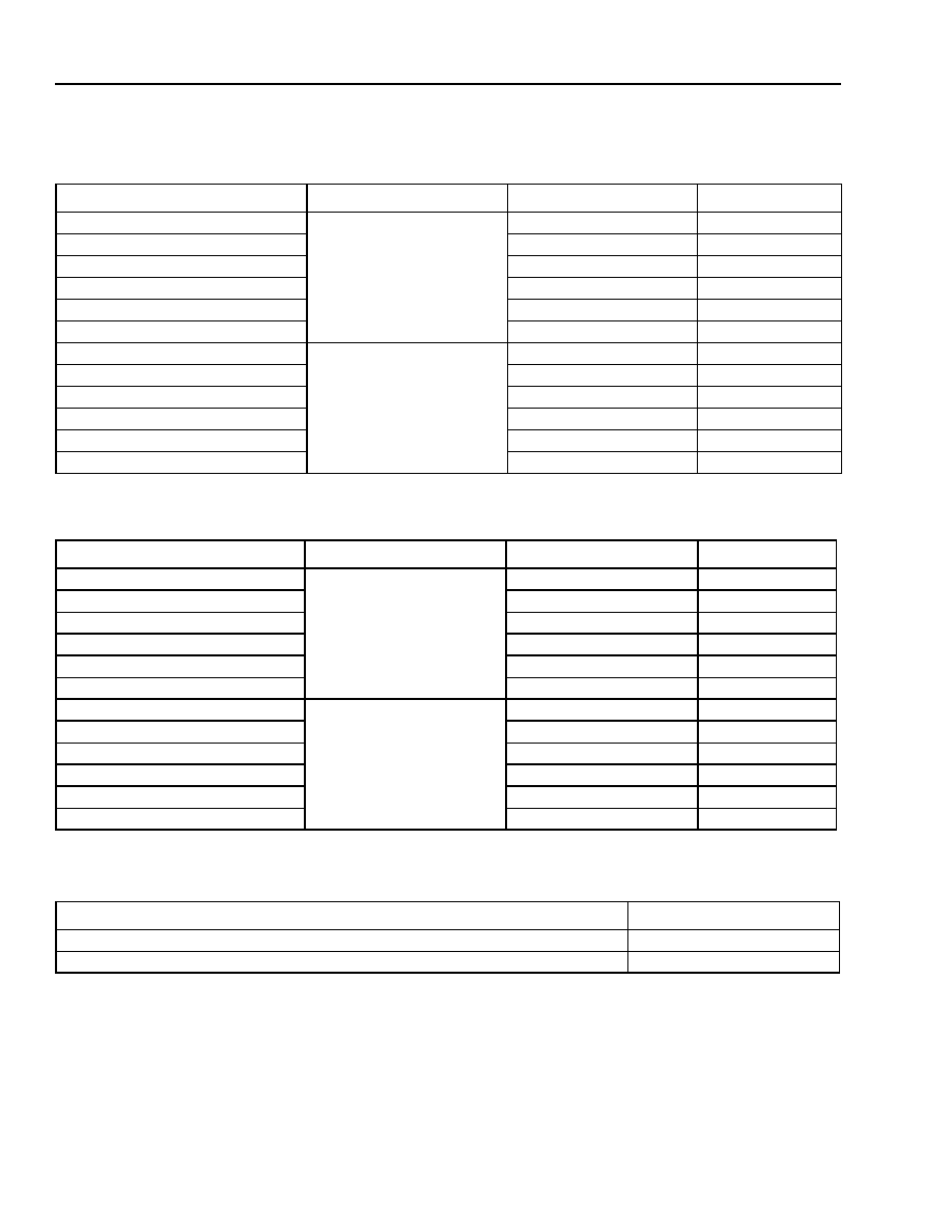
Characteristics
Minimum and maximum values specified over operating case temperature range and end-of-life (EOL). Typical val-
ues are measured at beginning-of-life (BOL) room temperature unless otherwise noted.
Table 1. Electrical Characteristics
1. Customers have the option for either a +5 V or ≠5 V supply.
2. Includes approximately 50 mA of DATA and CLOCK output termination current.
3. Measured with 50
load terminated to (V
CC
≠ 2.00) V.
4. DATA and CLOCK outputs are 10K ECL compatible.
5. Measured as shown in Figure 4.
6. Measured with an input data pseudorandom word 2
23
≠ 1.
Parameter
Symbol
Min
Typ
Max
Unit
dc Power Supply Voltages
V
CC
4.75
5.0
5.25
V
PIN Photodetector Supply Voltage (Pin 10)
1
V
PIN
V
PIN
4.75
≠5.25
5.0
≠5.0
5.25
≠4.75
V
V
dc Power Supply Currents:
2
OC-3/STM-1 Version
OC-12/STM-4 Version
I
CC
I
CC
--
--
110
150
150
200
mA
mA
Output Data/Clock Voltage:
3, 4
Low
High
V
OL
V
OH
V
CC
≠ 1.95
V
CC
≠ 1.03
--
V
CC
≠ 1.63
V
CC
≠ 0.88
V
V
Output Data/Clock Rise and Fall Time:
OC-3/STM-1 Version
OC-12/STM-4 Version
t
R
/t
F
t
R
/t
F
1100
320
1300
360
1700
500
ps
ps
Output Flag Voltage:
Low
High
VF
L
VF
H
0
V
CC
≠ 0.5
--
--
0.6
V
CC
V
V
Clock/Data Alignment:
5
OC-3/STM-1 Version
OC-12/STM-4 Version
T
CDA
T
CDA
≠800
≠300
--
--
800
300
ps
ps
Clock Duty Cycle
dc
45
--
55
%
Output Clock Random Jitter:
6
OC-3/STM-1 Version
OC-12/STM-4 Version
J
C
J
C
--
--
0.003
0.005
0.008
0.01
UI
UI
Output Clock Jitter Peaking
J
P
0.04
0.05
0.1
dB
Jitter Tolerance
Telcordia Technologies
GR-253-CORE and ITU-T G.958 Compliant
Jitter Transfer
Telcordia Technologies
GR-253-CORE and ITU-T G.958 Compliant

7
Agere Systems Inc.
Data Sheet
1345-Type Receiver with
January 2000
Clock Recovery and Data Retiming
Characteristics
(continued)
Table 2. Optical Characteristics
*
For a 1 x 10
≠10
BER. Measured with a 2
23
≠ 1 pseudorandom word optical input having a 50% average duty cycle.
Whenever the flag output is deasserted (logic low), the DATA and CLOCK outputs are silenced. See the Flag Output section on
page 2 for the DATA and CLOCK output signal levels.
Power supply noise in excess of 50 mVp-p may degrade the performance of the receiver. See User Interface section for recom-
mended power supply filtering.
1-725(C)
Figure 4. Clock/Data Alignment
Parameter
Symbol
Data Rates
Mbits/s
Min
Typ
Max
*
Unit
Measured Average Sensitivity:*
,
OC-3
OC-12
P
RL
P
RL
OC-3/STM-1
OC-12/STM-4
--
--
38
≠32.5
≠36
≠30
dBm
dBm
Maximum Input Power
P
MAX
OC-3/STM-1
OC-12/STM-4
0
≠6
2
≠4
--
--
dBm
dBm
Link Status Flag Threshold:
Decreasing Light Input
Decreasing Light Input
LST
D
LST
I
OC-3/STM-1
OC-12/STM-4
OC-3/STM-1
OC-12/STM-4
≠50
≠50
≠50
≠50
≠41
≠38.8
≠38
≠35
≠37.5
≠32.5
≠37.0
≠32.0
dBm
dBm
dBm
dBm
Flag Hysteresis
HYS
155/622
0.5
3
6
dB
Flag Response Time
t
FLAG
155/622
3
--
100
µ
s
Detector Responsivity
R
155/622
0.7
0.8
1.2
A/W
50%
50%
CLOCK
OUT
DATA
OUT
T
CDA

8
Agere Systems Inc.
1345-Type Receiver with
Data Sheet
Clock Recovery and Data Retiming
January 2000
PWB Layout Guidelines
s
Follow high-speed ECL design rules.
s
All high-speed output lines must be controlled-impedance lines, and the termination impedance must match
the line impedance. Controlled-impedance interruptions should be avoided (i.e., 90∞ bends, etc.) and paired lines
(i.e., DATA and
DATA
) should be of equal length.
s
Each output line should be terminated at the end of the line and must have a bypass capacitor on the voltage
side of the resistor for each termination.
s
Data and clock output lines should be as short and as straight as possible and isolated from noise sources (and
each other) to prevent noise from feeding back into the receiver.
s
Noise that couples into the receiver through the power supply pins can degrade device performance. See
Figure 2 for an example of power supply filtering for the receiver 5 V power supply pins.
s
Use a multilayer board so that the ground plane surrounds the areas occupied by the receiver and directly under-
neath it. Directly attach all pins listed as ground pins to the ground plane with no additional lead length.
All unused outputs must be terminated as shown. All resistors are 1/8 W, thin-film, ceramic chips. All capacitors are
25 Vdc, ceramic X7R or equivalent.
Qualification and Reliability
To help ensure high product reliability and customer satisfaction, Agere Systems is committed to an intensive qual-
ity program that starts in the design phase and proceeds through the manufacturing process. Optoelectronics mod-
ules are qualified to Agere Systems internal standards using MIL-STD-883 test methods and procedures and using
sampling techniques consistent with
Telcordia Technologies
requirements. The 1345 series of receivers have
undergone an extensive and rigorous set of qualification tests. This qualification program fully meets the intent of
Telcordia Technologies
reliability practices TR-NWT-000468 and TA-NWT-000983. In addition, the design, develop-
ment, and manufacturing facility of the Optoelectronics unit at Agere Systems is certified to be in full compliance
with the latest
ISO
Æ
-9001 Quality System Standards.
9
Agere Systems Inc.
Data Sheet
1345-Type Receiver with
January 2000
Clock Recovery and Data Retiming
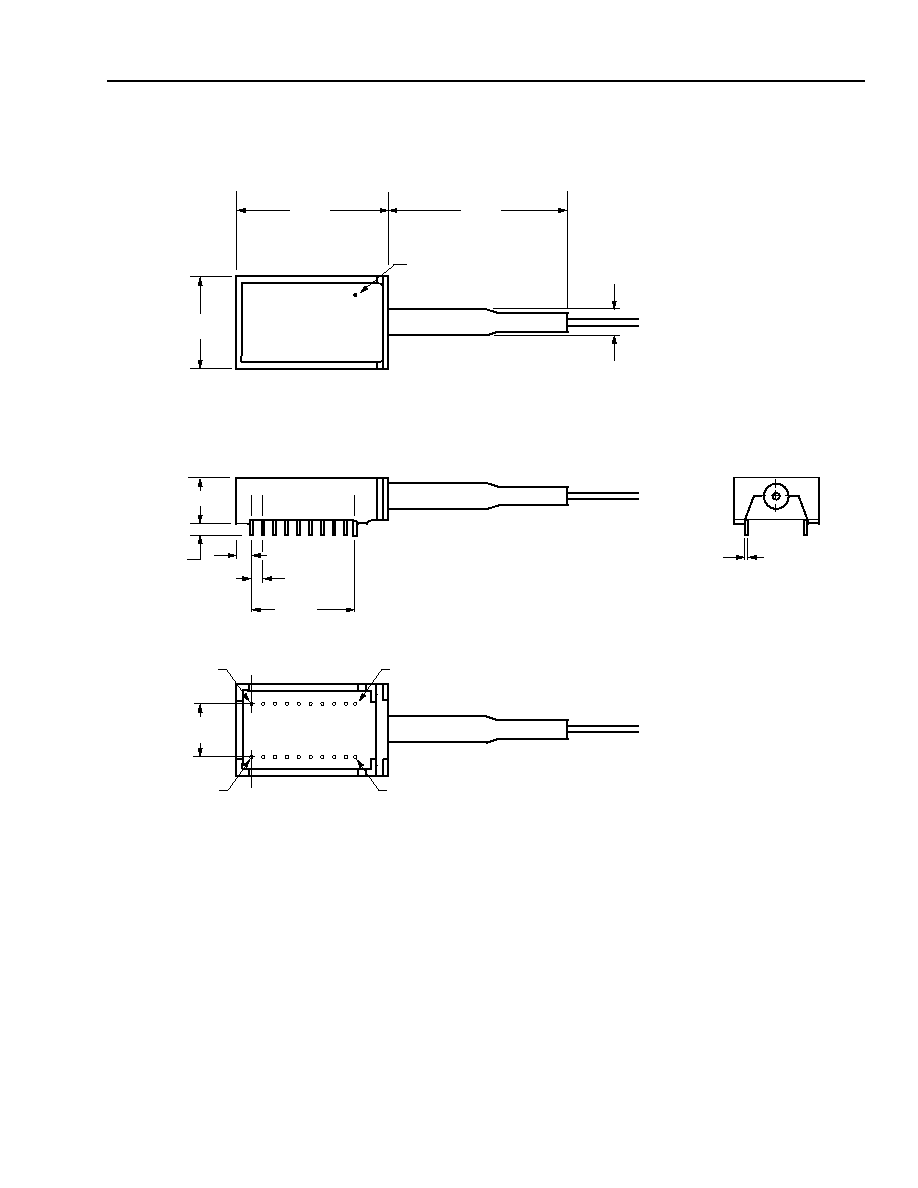
Outline Drawings
Dimensions are in inches and (millimeters). Unless noted otherwise, tolerances are ±0.005 in. (±0.127 mm).
1-988(C)
1.339
(34.01)
0.968
(24.58)
0.635
(16.14)
0.147
(3.73)
TOP VIEW
PIN 1 INDICATOR
0.125
(3.17)
0.110
(2.80)
0.100
(2.54)
0.900
(22.86)
0.350 (8.89)
0.400
(10.16)
PIN 20
PIN 11
PIN 1
PIN 10
0.018
(0.46)
10
Agere Systems Inc.
1345-Type Receiver with
Data Sheet
Clock Recovery and Data Retiming
January 2000
Ordering Information
Table 3. OC-3/STM-1 Receiver Versions
* These versions have nonsquelching data and clock outputs. See Nonsquelched Data and Clock Outputs section on page 2.
Table 4. OC-12/STM-4 Receiver Versions
* These versions have nonsquelching data and clock outputs. See Nonsquelched Data and Clock Outputs section on page 2.
Table 5. Related Products
Device Code
Pin 10 Requirements
Connector
Comcode
1345FMPC
No
Internal
Connections
FC-PC
108339979
1345CMPC
SC
108354473
1345TMPC
ST
Æ
108572421
1345FMPD
*
FC-PC
108354515
1345CMPD
*
SC
108354481
1345TMPD
*
ST
108572439
1345FAPC
Requires
+5 V
or
≠5 V
FC-PC
108468687
1345CAPC
SC
108359175
1345TAPC
ST
108572249
1345FAPD*
FC-PC
108572322
1345CAPD*
SC
108572280
1345TAPD*
ST
108572389
Device Code
Pin 10 Requirements
Connector
Comcode
1345FNPC
No
Internal
Connections
FC-PC
108155722
1345CNPC
SC
107354499
1345TNPC
ST
108572447
1345FNPD
*
FC-PC
108354523
1345CNPD
*
SC
108354507
1345TNPD*
ST
108572454
1345FBPC
Requires
+5 V
or
≠5 V
FC-PC
108572355
1345CBPC
SC
108572298
1345TBPC
ST
108572397
1345FBPD*
FC-PC
108573965
1345CBPD*
SC
108572306
1345TBPD*
ST
108572413
Description
Document Number
1241/1243/1245-Type Receivers for SONET/SDH Applications
DS99-073LWP
1340-Type Receiver with Clock Recovery and Data Retiming
DS00-098LWP

11
Agere Systems Inc.
Data Sheet
1345-Type Receiver with
January 2000
Clock Recovery and Data Retiming
Notes

1345-Type Receiver with Data Sheet
Clock Recovery and Data Retiming January 2000
Agere Systems Inc. reserves the right to make changes to the product(s) or information contained herein without notice. No liability is assumed as a result of their use or application.
ST is a
registered trademark of Agere Systems Inc.
Copyright © 2001 Agere Systems Inc.
All Rights Reserved
January 2000
DS00-099OPTO (Replaces DS99-071LWP)
For additional information, contact your Agere Systems Account Manager or the following:
INTERNET: http://www.agere.com
E-MAIL: docmaster@agere.com
N. AMERICA:
Agere Systems Inc., 555 Union Boulevard, Room 30L-15P-BA, Allentown, PA 18109-3286
1-800-372-2447, FAX 610-712-4106 (In CANADA: 1-800-553-2448, FAX 610-712-4106)
ASIA: Agere Systems Hong Kong Ltd., Suites 3201 & 3210-12, 32/F, Tower 2, The Gateway, Harbour City, Kowloon
Tel. (852) 3129-2000, FAX (852) 3129-2020
CHINA: (86) 21-5047-1212 (Shanghai), (86) 10-6522-5566 (Beijing), (86) 755-695-7224 (Shenzhen)
JAPAN: (81) 3-5421-1600 (Tokyo), KOREA: (82) 2-767-1850 (Seoul), SINGAPORE: (65) 778-8833, TAIWAN: (886) 2-2725-5858 (Taipei)
EUROPE: Tel. (44) 7000 624624, FAX (44) 1344 488 045
Telcordia Technologies
is a trademark of Telcordia Technologies Inc.
EIA
is a registered trademark of Electronic Industries Association.
Signetics
is a registered trademark of Signetics Corp.
National Semiconductor
is a registered trademark of National Semiconductor Corporation.
ISO
is a registered trademark of The International Organization for Standardization.