 | –≠–ª–µ–∫—Ç—Ä–æ–Ω–Ω—ã–π –∫–æ–º–ø–æ–Ω–µ–Ω—Ç: 1417H5 | –°–∫–∞—á–∞—Ç—å:  PDF PDF  ZIP ZIP |
NetLight
Æ
1417G5 and 1417H5-Type
ATM/SONET/SDH Transceivers with Clock Recovery
Data Sheet
January 2000
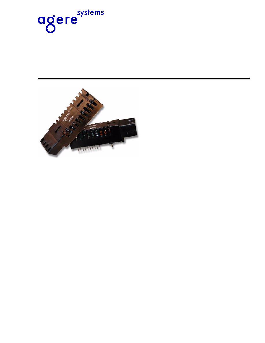
Available in a small form factor, RJ-45 size, plastic package,
the 1417G5 and 1417H5-Type are high-performance, cost-
effective transceivers for ATM/SONET/SDH applications at
155 Mbits/s and 622 Mbits/s.
Features
s
SONET/SDH Compliant (ITU-T G.957 Specifica-
tions)
-- IR-1/S1.1, S4.1
s
Small form factor, RJ-45 size, multisourced 20-pin
package
s
Requires single 3.3 V power supply
s
Clock recovery
s
LC duplex receptacle
s
Analog alarm outputs
s
Uncooled 1300 nm laser transmitter with automatic
output power control
s
Transmitter disable input
s
Wide dynamic range receiver with InGaAs PIN
photodetector
s
LVTTL signal-detect output
s
Low power dissipation
s
Raised ECL (PECL) logic data and clock interfaces
s
Operating case temperature range: ≠40
∞
C to
+85
∞
C
s
Agere Systems Inc. Reliability and Qualification
Program for built-in quality and reliability
Description
The 1417G5 and 1417H5 transceivers are high-
speed, cost-effective optical transceivers that are
compliant with the International Telecommunication
Union Telecommunication (ITU-T) G.957 specifica-
tions for use in ATM, SONET, and SDH applications.
The 1417G5 operates at the OC-3/STM-1 rate of
155 Mbits/s, and the 1417H5 operates at the OC-12/
STM-4 rate of 622 Mbits/s. The transceiver features
Agere Systems high-reliability optics and is pack-
aged in a narrow-width plastic housing with an LC
duplex receptacle. This receptacle fits into an RJ-45
form factor outline. The 20-pin package and pinout
conform to a multisource transceiver agreement.
The transmitter features differential PECL logic level
data inputs and a LVTTL logic level disable input. The
receiver features differential PECL logic level data
and clock outputs and a LVTTL logic level signal-
detect output.
2
Agere Systems Inc.
NetLight 1417G5 and 1417H5-Type
Data Sheet
ATM/SONET/SDH Transceivers with Clock Recovery
January 2000
Absolute Maximum Ratings
Stresses in excess of the absolute maximum ratings can cause permanent damage to the device. These are abso-
lute stress ratings only. Functional operation of the device is not implied at these or any other conditions in excess
of those given in the operations sections of the data sheet. Exposure to absolute maximum ratings for extended
periods can adversely affect device reliability.
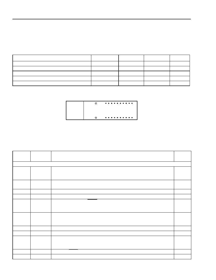
Pin Information
1-967(F).b
Figure 1. 1417G5 and 1714H5 Transceivers, 20-Pin Configuration, Top View
Table 1. Transceiver Pin Descriptions
Parameter
Symbol
Min
Max
Unit
Supply Voltage
V
CC
0
3.6
V
Operating Case Temperature Range
T
C
≠40
85
∞
C
Storage Case Temperature Range
T
stg
≠40
85
∞
C
Lead Soldering Temperature/Time
--
--
250/10
∞
C/s
Operating Wavelength Range
1.1
1.6
nm
Pin
Number
Symbol
Name/Description
Logic
Family
Receiver
MS
MS
Mounting Studs. The mounting studs are provided for transceiver mechani-
cal attachment to the circuit board. They may also provide an optional con-
nection of the transceiver to the equipment chassis ground.
NA
1
Photode-
tector Bias
Photodetector Bias. This lead supplies bias for the PIN photodetector diode.
NA
2
V
EER
Receiver Signal Ground.
NA
3
V
EER
Receiver Signal Ground.
NA
4
CLK≠
Received Recovered Clock Out. The rising edge occurs at the rising edge of
the received data output. The falling edge occurs in the middle of the received
data bit period.
PECL
5
CLK+
Received Recovered Clock Out. The falling edge occurs at the rising edge
of the received data output. The rising edge occurs in the middle of the
received data bit period.
PECL
6
V
EER
Receiver Signal Ground.
NA
7
V
CCR
Receiver Power Supply.
NA
8
SD
Signal Detect.
Normal operation: logic one output.
Fault condition: logic zero output.
LVTTL
9
RD≠
Received DATA Out. No internal terminations will be provided.
PECL
10
RD+
Received DATA Out. No internal terminations will be provided.
PECL
6 7 8 9 10
15 14 13 12 11
20-PIN MODULE - TOP VIEW
TX
RX
1 2 3 4 5
20 19 18 17 16
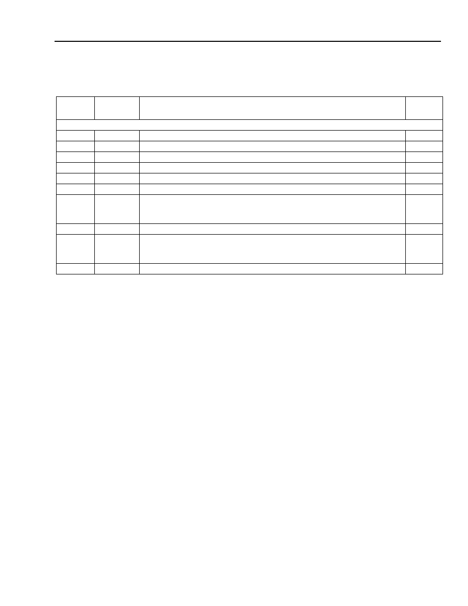
3
Agere Systems Inc.
Data Sheet
NetLight 1417G5 and 1417H5-Type
January 2000
ATM/SONET/SDH Transceivers with Clock Recovery
Transmitter
11
V
CCT
Transmitter Power Supply.
NA
12
V
EET
Transmitter Signal Ground.
NA
13
T
DIS
Transmitter Disable.
LVTTL
14
TD+
Transmitter Data In. PECL
15
TD≠
Transmitter Data In Bar.
PECL
16
V
EET
Transmitter Signal Ground.
NA
17
B
MON
(≠)
Laser Diode Bias Current Monitor--Negative End. The laser bias current
is accessible as a dc-voltage by measuring the voltage developed across pins
17 and 18.
NA
18
B
MON
(+)
Laser Diode Bias Current Monitor--Positive End. See pin 17 description.
NA
19
P
MON
(≠)
Laser Diode Optical Power Monitor--Negative End. The back-facet diode
monitor current is accessible as a dc-voltage by measuring the voltage devel-
oped across pins 19 and 20.
NA
20
P
MON
(+)
Laser Diode Optical Power Monitor--Positive End. See pin 19 description.
NA
Pin
Number
Symbol
Name/Description
Logic
Family
Electrostatic Discharge
Caution: This device is susceptible to damage as
a result of electrostatic discharge (ESD).
Take proper precautions during both
handling and testing. Follow
EIA
Æ
stan-
dard
EIA
-625.
Although protection circuitry is designed into the
device, take proper precautions to avoid exposure to
ESD. Agere Systems employs a human-body model
(HBM) for ESD-susceptibility testing and protection-
design evaluation. ESD voltage thresholds are depen-
dent on the critical parameters used to define the
model. A standard HBM (resistance = 1.5 k
, capaci-
tance = 100 pF) is widely used and, therefore, can be
used for comparison purposes. The HBM ESD thresh-
old established for the 1417G5 and 1417H5 transceiv-
ers is
±
1000 V.
Application Information
The 1417 receiver section is a highly sensitive fiber-
optic receiver. Although the data outputs are digital
logic levels (PECL), the device should be thought of as
an analog component. When laying out system appli-
cation boards, the 1417 transceiver should receive the
same type of consideration one would give to a sensi-
tive analog component.
Printed-Wiring Board Layout Considerations
A fiber-optic receiver employs a very high-gain, wide-
bandwidth transimpedance amplifier. This amplifier
detects and amplifies signals that are only tens of nA in
amplitude when the receiver is operating near its sensi-
tivity limit. Any unwanted signal currents that couple
into the receiver circuitry cause a decrease in the
receiver's sensitivity and can also degrade the perfor-
mance of the receiver's signal detect (SD) circuit. To
minimize the coupling of unwanted noise into the
receiver, careful attention must be given to the printed-
wiring board.
At a minimum, a double-sided printed-wiring board
(PWB) with a large component-side ground plane
beneath the transceiver must be used. In applications
that include many other high-speed devices, a multi-
layer PWB is highly recommended. This permits the
placement of power and ground on separate layers,
which allows them to be isolated from the signal lines.
Multilayer construction also permits the routing of sen-
sitive signal traces away from high-level, high-speed
signal lines. To minimize the possibility of coupling
noise into the receiver section, high-level, high-speed
signals such as transmitter inputs and clock lines
should be routed as far away as possible from the
receiver pins.
Pin Information
(continued)
Table 1. Transceiver Pin Descriptions (continued)
4
4
Agere Systems Inc.
NetLight 1417G5 and 1417H5-Type
Data Sheet
ATM/SONET/SDH Transceivers with Clock Recovery
January 2000
Application Information
(continued)
Noise that couples into the receiver through the power
supply pins can also degrade performance. It is recom-
mended that the pi filter, shown in Figure 2, be used for
both the transmitter and receiver power supplies.
Data Clock and Signal Detect Outputs
The data clock and signal detect outputs of the 1417
transceiver are driven by open-emitter NPN transistors,
which have an output impedance of approximately 7
.
Each output can provide approximately 50 mA maxi-
mum current to a 50
load terminated to V
CC
≠ 2.0 V.
Due to the high switching speeds of ECL outputs,
transmission line design must be used to interconnect
components. To ensure optimum signal fidelity, both
data outputs (RD+/RD≠) and clock outputs (CLK+/
CLK≠) should be terminated identically. The signal
lines connecting the data and clock outputs to the next
device should be equal in length and have matched
impedances. Controlled impedance stripline or micros-
trip construction must be used to preserve the quality
of the signal into the next component and to minimize
reflections back into the receiver, which could degrade
its performance. Excessive ringing due to reflections
caused by improperly terminated signal lines makes it
difficult for the component receiving these signals to
decipher the proper logic levels and can cause transi-
tions to occur where none were intended. Also, by min-
imizing high-frequency ringing, possible EMI problems
can be avoided.
The signal-detect output is LVTTL logic. A logic low at
this output indicates that the optical signal into the
receiver has been interrupted or that the light level has
fallen below the minimum signal detect threshold. This
output should not be used as an error rate indicator,
since its switching threshold is determined only by the
magnitude of the incoming optical signal.
Transceiver Processing
When the process plug is placed in the transceiver's
optical port, the transceiver and plug can withstand
normal wave soldering and aqueous spray cleaning
processes. However, the transceiver is not hermetic,
and should not be subjected to immersion in cleaning
solvents. The transceiver case should not be exposed
to temperatures in excess of 125
∞
C. The transceiver
pins can be wave soldered at 250
∞
C for up to 10 sec-
onds. The process plug should only be used once.
After removing the process plug from the transceiver, it
must not be used again as a process plug; however, if it
has not been contaminated, it can be reused as a dust
cover.
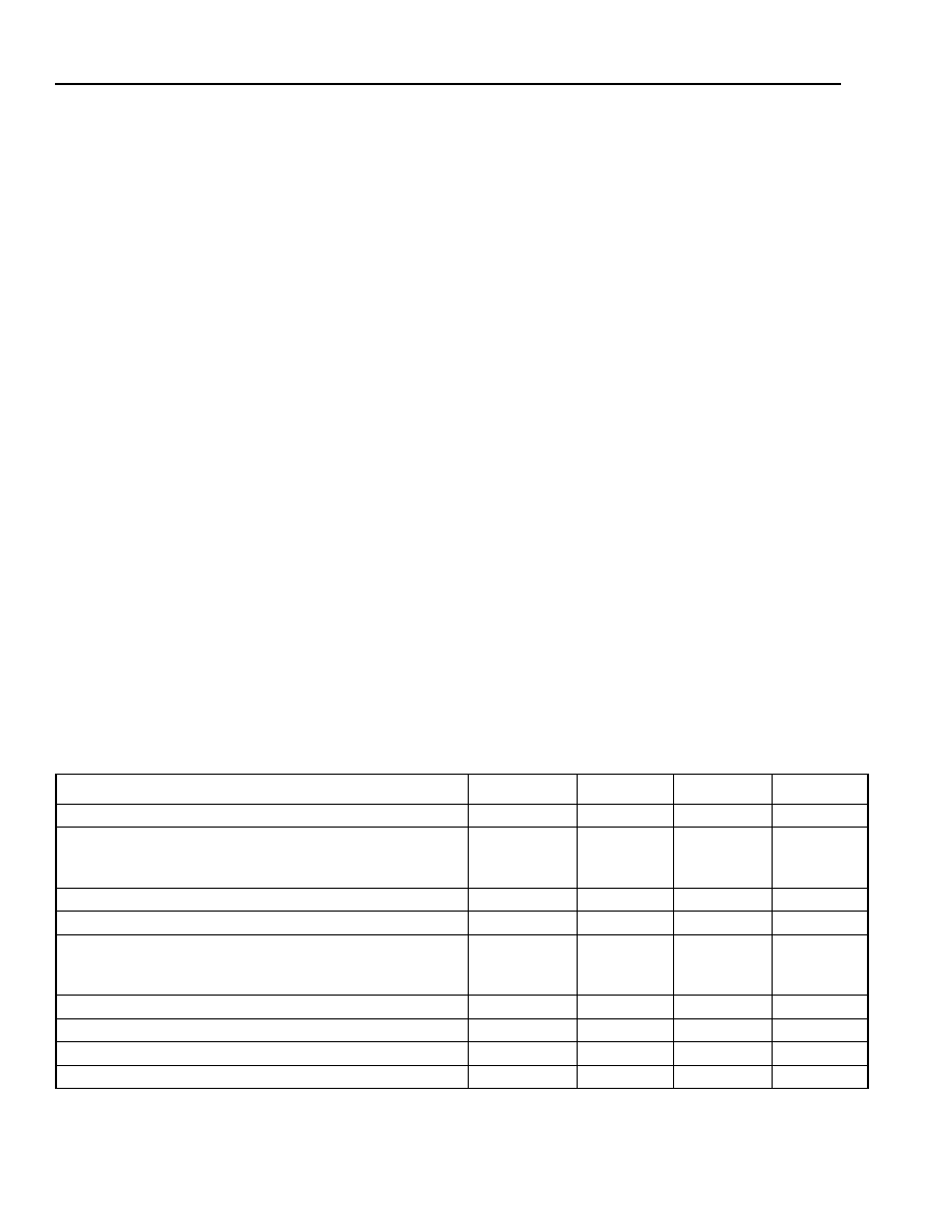
Transceiver Optical and Electrical Characteristics
Table 2. Transmitter Optical and Electrical Characteristics (T
C
= ≠40
∞
C to +85
∞
C; V
CC
= 3.135 V to 3.465 V)
Parameter
Symbol
Min
Max
Unit
Average Optical Output Power (EOL)
P
O
≠15.0
≠8.0
dBm
Optical Wavelength:
STM-1 (4 nm spectral width, maximum)
STM-4 (2.5 nm spectral width, maximum)
C
1261
1274
1360
1356
nm
nm
Dynamic Extinction Ratio
EXT
8.2
--
dB
Power Supply Current
I
CCT
--
150
mA
Input Data Voltage:
Low
High
V
IL
V
IH
V
CC
≠ 1.81
V
CC
≠ 1.025
V
CC
≠ 1.62
V
CC
≠ 0.88
V
V
Transmit Disable Voltage
V
D
V
CC
≠ 1.3
V
CC
V
Transmit Enable Voltage
V
EN
V
EE
V
EE
+ 0.8
V
Laser Bias Voltage
V
BIAS
0
0.70
V
Laser Back-facet Monitor Voltage
V
BF
0.01
0.20
V
5
Agere Systems Inc.
Data Sheet
NetLight 1417G5 and 1417H5-Type
January 2000
ATM/SONET/SDH Transceivers with Clock Recovery
Transceiver Optical and Electrical Characteristics
(continued)
Table 3. Receiver Optical and Electrical Characteristics (T
C
= ≠40
∞
C to +85
∞
C; V
CC
= 3.135 V to 3.465 V)
* For 1 x 10
≠10
BER with an optical input using 2
23
≠ 1 PRBS.
Typical rise and fall time is 360 ps.
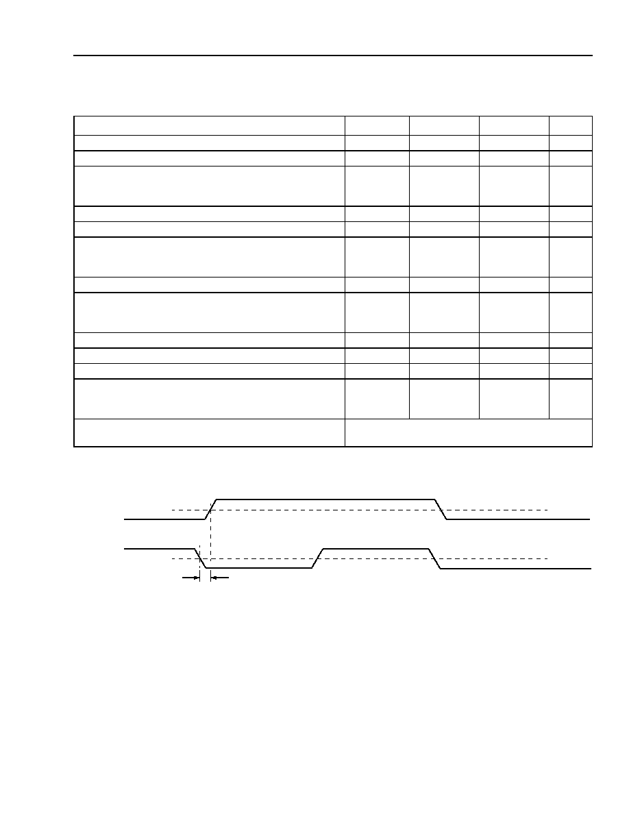
1-725(F).b
Figure 2. Clock/Data Alignment
Parameter
Symbol
Min
Max
Unit
Average Sensitivity (STM-1/STM-4)*
P
I
--
≠28
dBm
Maximum Input Power*
P
MAX
≠8
--
dBm
Link Status Switching Threshold:
Decreasing Light (STM-1/STM-4)
Increasing Light (STM-1/STM-4)
LST
D
LST
I
≠45
≠45
≠29.0
≠28.5
dBm
dBm
Link Status Hysteresis
HYS
0.5
--
dB
Power Supply Current
I
CCR
--
200
mA
Output Data Voltage/Clock Voltage:
Low
High
V
OL
V
OH
V
CC
≠ 1.81
V
CC
≠ 1.025
V
CC
≠ 1.62
V
CC
≠ 0.88
V
V
Output Data/Clock Rise and Fall Times
t
R
/t
F
300
500
ps
Signal Detect Output Voltage:
Low
High
V
OL
V
OH
0.0
2.4
0.8
V
CC
V
V
Clock Duty Cycle
DC
45
55
%
Output Clock Random Jitter
J
C
--
0.01
UI
Output Clock Random Jitter Peaking
J
P
--
0.1
dB
Clock/Data Alignment: (See Figure 2.)
STM-1
STM-4
TCDA
≠800
≠200
800
200
ns
ns
Jitter Tolerance/Jitter Transfer
Telcordia Technologies
Æ
GR-253-Core and
ITU-TG.958 Compliant
50%
50%
CLOCK
OUT
DATA
OUT
T
CDA
6
Agere Systems Inc.
NetLight 1417G5 and 1417H5-Type
Data Sheet
ATM/SONET/SDH Transceivers with Clock Recovery
January 2000
Qualification and Reliability
To help ensure high product reliability and customer satisfaction, Agere Systems is committed to an intensive qual-
ity program that starts in the design phase and proceeds through the manufacturing process. Optoelectronic mod-
ules are qualified to Agere Systems internal standards using MIL-STD-883 test methods and procedures and using
sampling techniques consistent with
Telcordia Technologies
requirements. The 1417 transceiver is required to pass
an extensive and rigorous set of qualification tests.
This qualification program fully meets the intent of
Telcordia Technologies
reliability practices TR-NWT-000468 and
TA-TSY-000983 requirements. In addition, the design, development, and manufacturing facilities of Agere Systems
Optoelectronics unit have been certified to be in full compliance with the latest
ISO
Æ
9001 quality system stan-
dards.
Electrical Schematic
1-968(F).b
* Ferrite beads can be used as an option.
For all capacitors, MLC caps are recommended.
Figure 3. Power Supply Filtering for the Small Form Factor Transceiver
L1 = L2 = 1
µ
H--4.7
µ
H*
C1 = C2 = 10 nF
C3 = 4.7
µ
F--10
µ
F
C4 = C5 = 4.7
µ
F--10
µ
F
RECEIVER
POST-
AMPLIFIER/
CDR
17 18 19 20
TD≠
TD+
V
EET
12, 16
15
14
P
R
EA
MP
RD+
RD≠
SD
V
EER
V
CCT
V
CCR
SFF TRANSCEIVER
10
9
8
2, 3, 6
11
7
C4
C5
C2
C3
C1
V
CC
L2
L1
B
MON≠
B
MON+
P
MON≠
P
MON+
T
DIS
13
CLK+
CLK≠
5
4
V
PD
1
TRANSMITTER
DRIVER
15
15
10
15
15
200
7
Agere Systems Inc.
Data Sheet
NetLight 1417G5 and 1417H5-Type
January 2000
ATM/SONET/SDH Transceivers with Clock Recovery
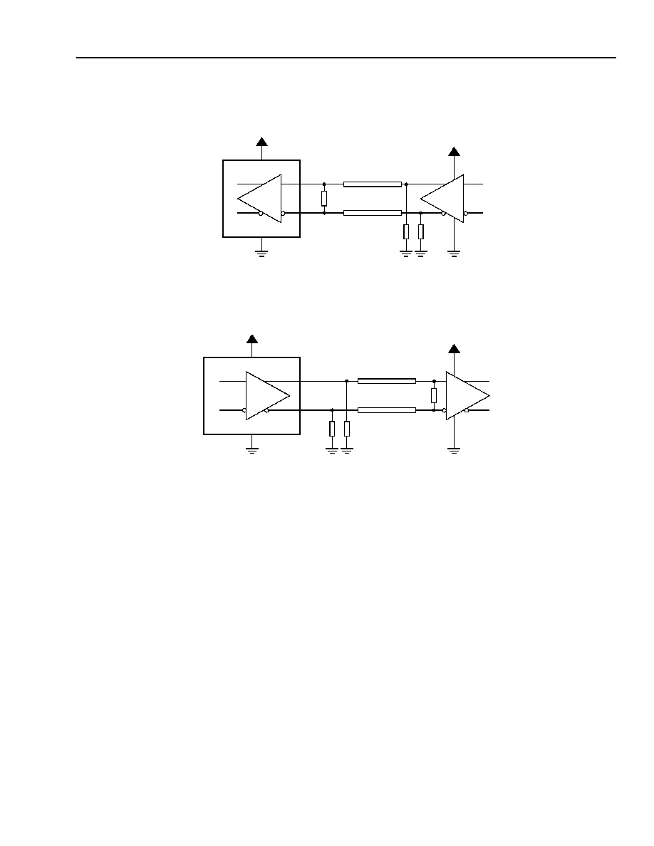
Application Schematics
1-970(F).b
Figure 4. 3.3 V Transceiver Interface with 3.3 V ICs
TD+
TD≠
100
LVPECL
130
130
V
CC
(3.3 V)
V
CC
(3.3 V)
A. Transmitter Interface (LVPECL to LVPECL)
RD+/CLK+
RD≠/CLK≠
LVPECL
V
CC
(3.3 V)
V
CC
(3.3 V)
100
130
130
B. Receiver Interface (LVPECL to LVPECL)
Z = 50
Z = 50
Z = 50
Z = 50
8
Agere Systems Inc.
NetLight 1417G5 and 1417H5-Type
Data Sheet
ATM/SONET/SDH Transceivers with Clock Recovery
January 2000
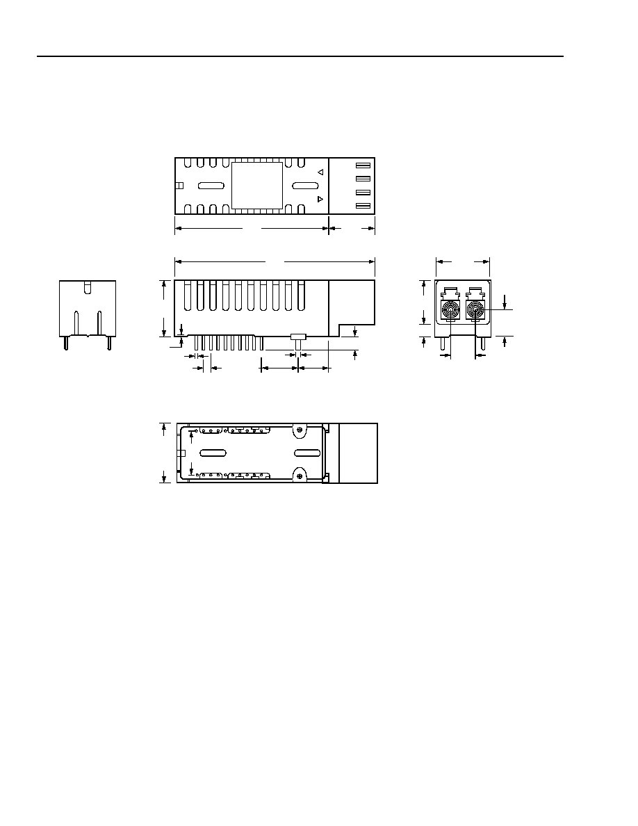
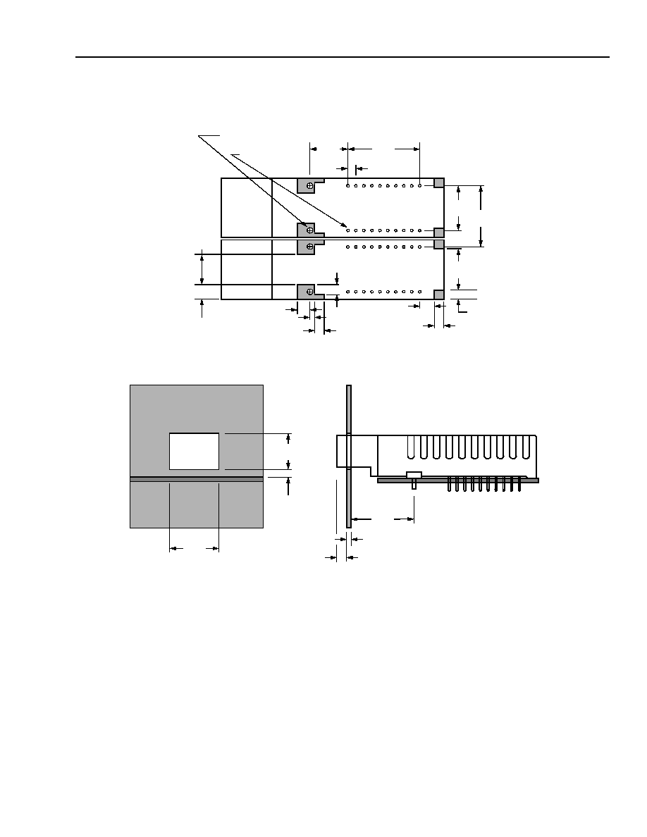
Outline Diagrams
Package Outline
Dimensions are in inches and (millimeters).
1-1086(F)
* Dimension does not comply with multisource agreement.
1.907
0.500*
0.014 (0.36)
0.070 (1.78)
0.125 (3.17)
0.299 (7.59)
0.040 (1.02)
0.018 (0.46)
0.4
0
0
(48.44)
(12.70)
(10
.
16)
0.5
35 M
A
X
(13
.
59)
0.350 (8.89)
0.385
0.115
0.246
(9.78)
(2.92)
(6.25)
0.251
(6.38)
0.512
(13.00)
1417
TRANSCEIVER
0.433
1.474
1.907
0.500*
0.014 (0.36)
0.070 (1.78)
0.125 (3.17)
0.299 (7.59)
0.040 (1.02)
0.018 (0.46)
0.4
0
0
(37.44)
(11.00)
(48.44)
(12.70)
(10
.
16)
0.5
35 M
A
X
(13
.
59)
0.350 (8.89)
0.385
0.115
0.246
(9.78)
(2.92)
(6.25)
0.251
(6.38)
0.512
(13.00)
AG
ERE
SYS
TE
M
S
9
Agere Systems Inc.
Data Sheet
NetLight 1417G5 and 1417H5-Type
January 2000
ATM/SONET/SDH Transceivers with Clock Recovery
Outline Diagrams
(continued)
Printed-Wiring Board Layout* and Recommended Panel Opening
1-1088(F)
* Per multisource agreement.
0.582
(14.78)
0.550
(13.97)
0.400
(10.20)
0.039
(1.00)
0.113
(2.87)
0.105
(2.67)
0.300
(7.62)
0.118
(3.00)
0.630
(15.75)
0.070
(1.78)
0.350
(8.89)
2.00
(0.079)
0.121
(3.07)
0.079
(3.00)
0.079
(3.00)
0.400
(10.20)
0.550
(13.97)
0.378
(9.60)
0.118
(3.00)
0.039
(1.00)
0.079
(2.00)
0.055 ± 0.004 DIA. 2X
(1.40 ± 0.1) DIA
0.032 ± 0.004 DIA. 20X
(0.81 ± 0.1) DIA
NetLight 1417G5 and 1417H5-Type
Data Sheet
ATM/SONET/SDH Transceivers with Clock Recovery
January 2000
Agere Systems Inc. reserves the right to make changes to the product(s) or information contained herein without notice. No liability is assumed as a result of their use or application.
NetLight is a registered trademark of Agere Systems Inc.
Copyright © 2001 Agere Systems Inc.
All Rights Reserved
January 2000
DS00-100OPTO (Replaces DS99-227LWP)
For additional information, contact your Agere Systems Account Manager or the following:
INTERNET:
http://www.agere.com
E-MAIL:
docmaster@agere.com
N. AMERICA:
Agere Systems Inc., 555 Union Boulevard, Room 30L-15P-BA, Allentown, PA 18109-3286
1-800-372-2447, FAX 610-712-4106 (In CANADA: 1-800-553-2448, FAX 610-712-4106)
ASIA:
Agere Systems Hong Kong Ltd., Suites 3201 & 3210-12, 32/F, Tower 2, The Gateway, Harbour City, Kowloon
Tel. (852) 3129-2000, FAX (852) 3129-2020
CHINA: (86) 21-5047-1212 (Shanghai), (86) 10-6522-5566 (Beijing), (86) 755-695-7224 (Shenzhen)
JAPAN: (81) 3-5421-1600 (Tokyo), KOREA: (82) 2-767-1850 (Seoul), SINGAPORE: (65) 778-8833, TAIWAN: (886) 2-2725-5858 (Taipei)
EUROPE:
Tel. (44) 7000 624624, FAX (44) 1344 488 045
Laser Safety Information
Class I Laser Product
FDA/CDRH Class I laser product. All versions of the transceiver are Class I laser products per CDRH, 21 CFR
1040 Laser Safety requirements. All versions are Class I laser products per
IEC
Æ
60825-1:1993. The transceiver
has been certified with the FDA under accession number 8720009.
CAUTION: Use of controls, adjustments, and procedures other than those specified herein may result in
hazardous laser radiation exposure.
This product complies with 21 CFR 1040.10 and 1040.11.
Wavelength = 1.3
µ
m
Maximum power = 0.2 mW
Because of size constraints, laser safety labeling (Including an FDA Class IIIb label) is not affixed to the module but
is attached to the outside of the shipping carton.
Product is not shipped with power supply.
NOTICE
Unterminated optical connectors may emit laser radiation.
Do not view with optical instruments.
Ordering Information
Table 4. Ordering Information
EIA
is a registered trademark of Electronic Industries Association.
Telcordia Technologies
is a trademark of Telcordia Technologies Inc.
IEC
is a registered trademark of The International Electrotechnical Commission.
ISO
is a registered trademark of The International Organization for Standardization.
Description
Device Code
Comcode
2 x 10 Single-mode Transceiver for OC-3 /STM-1 (155 Mbits/s)
with Clock Recovery
1417G5A
108416678
2 x 10 Single-mode Transceiver for OC-12 /STM-4 (622 Mbits/s)
with Clock Recovery
1417H5A
108416686

11
Agere Systems Inc.
Data Sheet
NetLight 1417G5 and 1417H5-Type
January 2000
ATM/SONET/SDH Transceivers with Clock Recovery

12
12
Agere Systems Inc.
NetLight 1417G5 and 1417H5-Type
Data Sheet
ATM/SONET/SDH Transceivers with Clock Recovery
January 2000