 | –≠–ª–µ–∫—Ç—Ä–æ–Ω–Ω—ã–π –∫–æ–º–ø–æ–Ω–µ–Ω—Ç: ATLANTA | –°–∫–∞—á–∞—Ç—å:  PDF PDF  ZIP ZIP |
Advance Product Brief
March 1997
LUC4AB01
ATM Buffer Manager (ABM)
Section 5.3
LUCENT TECHNOLOGIES--PROPRIETARY
Use pursuant to Company Instructions
Introduction
The ABM IC is part of the ATLANTA chip set consist-
ing of four devices that provide a highly integrated,
innovative, and complete VLSI solution for implement-
ing the ATM layer core of an ATM switch system. The
chip set enables construction of high-performance,
feature-rich, and cost-effective ATM switches, scalable
over a wide range of switching capacities. This docu-
ment discusses the ABM device.
Features
s
Provides input/output (bidirectional) queue manage-
ment for an N x N switch fabric (up to 25 Gbits/s
capacity) and up to 31 MPHY ports.
-- Handles full-duplex aggregate ATM traffic up to
622 Mbits/s (ingress and egress).
-- Queues up to 32K ATM cells in external memory
using standard synchronous SRAMs, organized
in a shared output buffered architecture*.
-- Supports four delay priorities per queue.
s
Uses programmable, weighted, round-robin algo-
rithm for flexibility in scheduling delay priority ser-
vice (can default to strict priority service).
s
On egress, provides programmable rate scheduling
of output queues for MPHY ports (from 1.2 Mbits/s
to 622 Mbits/s). Can also accommodate variable
rate PHY ports (e.g., SAR devices).
s
Performs multicasting (on egress side) for up to 30
MPHY output ports and one CPU port.
s
Incorporates an innovative adaptive dynamic
thresholding (ADT) algorithm for maximizing buffer
efficiency while ensuring fairness.
s
Provides range of congestion management options
and support for ABR.
-- Supports nonblocking backpressure feedback
from an external switch fabric.
-- Selective cell discard (CLP1, CLP0+1).
-- Optional EFCI marking (SEFCI on a per-connec-
tion basis) and support for CI/NI marking.
-- Optional EPD and PPD support.
-- Independent, configurable dynamic thresholds
available for each delay priority level to trigger
congestion management options. Can default to
static thresholding.
s
Supplies buffer congestion data to support an
optional external ER calculation engine for ABR flow
control.
s
Maintains an extensive variety of counters for statis-
tics gathering, facilitating network management soft-
ware.
s
Supports simultaneous links with dual-switch fabric
cards to facilitate redundant fabric operation.
s
Can be used in conjunction with LUC4AU01 ALM IC
to provide a complete stand-alone two-chip solution
for:
-- A 4 x 4 at 155 Mbits/s ATM shared memory
switch.
-- A 25 x 25 at 25 Mbits/s ATM shared memory
switch.
-- ATM multiplexor/concentrator applications.
s
Can be used in conjunction with an external switch
fabric (LUC4AS01 ASX and LUC4AC01 ACE ICs,
part of the ATLANTA chip set) to provide a scalable,
nonblocking switch solution.
s
Provides a generic,
Intel
or
Motorola
compatible,
16-bit microprocessor interface for configuration,
statistics, and maintenance.
s
Supports a scalable external memory interface with
synchronous SRAMs (20 ns cycle time).
s
Facilitates circuit board testing with on-chip
IEEE
ß
standard boundary scan.
s
Fabricated as a low-power, monolithic IC in 0.5
µ
m,
3.3 V CMOS technology, with 5 V-tolerant and TTL-
level compatible I/O.
s
Available in 352-pin PBGA package.
Intel
is a registered trademark of Intel Corporation.
Motorola
is a registered trademark of Motorola, Inc.
ß
IEEE
is a registered trademark of The Institute of Electrical and
Electronics Engineers, Inc.
* In half-duplex operation, the ABM can queue up to 64K ATM cells
in external memory using standard synchronous SRAMs.

2
2
Lucent Technologies Inc.
Advance Product Brief
March 1997
ATM Buffer Manager (ABM)
LUC4AB01
Section 5.3
LUCENT TECHNOLOGIES--PROPRIETARY
Use pursuant to Company Instructions
Description
Figure 1 shows the architecture of an ATM switch that
uses the ATLANTA chip set. The highly sophisticated
LUC4AB01 ATM Buffer Manager (ABM) chip provides
efficient queue management through the use of innova-
tive queuing and thresholding/congestion algorithms.
ATM cells are received over a UTOPIA II Plus interface
(ingress_rx data path) and queued in an ingress buffer
pool located in external memory. Here, they are sched-
uled to be transmitted to an external switch fabric
(ingress_tx data path). Alternatively, if the ABM is con-
figured to operate in stand-alone shared memory
switch mode (no external switch fabric is present), the
cells are transferred internally to the egress buffer pool.
5-4554r9
Figure 1. Architecture of an ATM Switch Using the ATLANTA Chip Set
ALM
LUC4AU01
MICROPROCESSOR
INTERFACE
SRAM
LINE CARD #1
#1
#1
LINE CARD #N
N x N SWITCH FABRIC
#N
BA
CKPLANE
REDUND
ANT BA
CKPLANE
ABM
LUC4AB01
SRAM
PHYSICAL LAYER
INTERFACE (MPHY)
ALM
LUC4AU01
SRAM
ABM
LUC4B01
SRAM
ASX
LUC4AS01
ACE
LUC4AC01
ASX
LUC4AS01
ASX
LUC4AS01
ACE
LUC4AC01
ASX
LUC4AS01
#1
#1
#N
N x N REDUNDANT SWITCH FABRIC
#N
ASX
LUC4AS01
ACE
LUC4AC01
ASX
LUC4AS01
ASX
LUC4AS01
ACE
LUC4AC01
ASX
LUC4AS01
#1
#1
#N
INGRESS DIRECTION
EGRESS DIRECTION
#1
#1
#N
#N
#N
#N
1
M
PHY PORTS
1
M
PHY PORTS
MICROPROCESSOR
INTERFACE
MICROPROCESSOR
INTERFACE
MICROPROCESSOR
INTERFACE
Lucent Technologies Inc.
3
Advance Product Brief
March 1997
ATM Buffer Manager (ABM)
LUC4AB01
Section 5.3
LUCENT TECHNOLOGIES--PROPRIETARY
Use pursuant to Company Instructions
Description
(continued)
ATM cells received from the switch fabric (egress_rx
data path) are queued in the egress buffer pool also
located in external memory. Here, they are scheduled
to be transmitted over the UTOPIA II Plus interface
toward MPHY ports.
The ABM processes cells on a time-slot (cell time)
basis. The ABM is capable of receiving and transmit-
ting one ingress cell and one egress cell each time
slot.
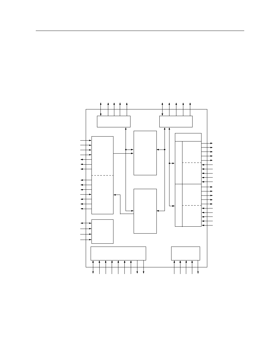
A block diagram and a brief description of the function-
ality of each block follows.
5-4694r5
Figure 2. ABM Block Diagram
IRSOC
INGRESS_TX
EGRESS_RX
EGRESS_RX
INGRESS_TX
SWITCH FABRIC
INTERFACE
PORT 0
PORT 1
IRDATA[7:0]
IRPRTY
IRCLKN
IRCLKP
EWSOC
EWDATA[7:0]
EWPRTY
EWCLKN
EWCLKP
INGRESS
QUEUE
PROCESSOR
EGRESS
QUEUE
PROCESSOR
JTAG
MICROPROCESSOR
INTERFACE
CELL DATA RAM
INTERFACE
POINTER RAM
INTERFACE
CONTROL
EGRESS_TX
INGRESS_RX
UTOPIA II
PLUS
INTERFACE
IWSOC
IWDATA[15:0]
IWPRTY
IWCLAV
IWENBN
IWADDR[4:0]
IWCLK
ERSOC
ERDATA[15:0]
ERPRTY
ERCLAV
ERENBN
ERADDR[4:0]
ERCLK
RIRSOC
RIRDATA[7:0]
RIRPRTY
RIRCLKN
RIRCLKP
REWSOC
REWDATA[7:0]
REWPRTY
REWCLKN
REWCLKP
GTSYNC
GOE
GRST
GCLK
MADDRLE
MDATA[15:0]
MADR[2:0]
MCSELN
MDIR
MRDYN
MDEN
MBUSMODE
MINTN
TMS
TCK
TDI
TRSTN
TDO
POEN
PDATA[17:0]
PADR[17:0]
PWEN
PCLK
DOEN
DDATA[63:0]
DADR[17:0]
DWEN
DCLK
TO/FROM ALM (OR OPTIONAL USER PROPRIETARY DEVICE)
TO/FROM SWITCH FABRIC (OPTIONAL)

4
4
Lucent Technologies Inc.
Advance Product Brief
March 1997
ATM Buffer Manager (ABM)
LUC4AB01
Section 5.3
LUCENT TECHNOLOGIES--PROPRIETARY
Use pursuant to Company Instructions
Description
(continued)
UTOPIA II "Plus" Interface (UTOP)
UTOP performs operations necessary to allow full-
duplex communication between the ABM and ALM (or
an external user proprietary device). It follows the UTO-
PIA II master protocol for 16-bit transfers described in
UTOPIA Level 2, V1.0, except that cell lengths may be
greater than 54 bytes. Every time-slot UTOP is capable
of performing an ingress receive operation and an
egress transmit operation.
Ingress Receive Operation
UTOP is capable of polling only one slave device on
the IWDATA[15:0] bus. It polls this slave device (e.g.
ALM) by driving IWADDR[4:0] with the user-pro-
grammed address located in CFG2_reg[12:8]. If the
slave device (e.g. ALM) has a cell available, it responds
by driving IWCLAV active one cycle later. The transfer
continues as described in UTOPIA Level 2, V1.0. The
cell is written into a FIFO and an internal cell available
is asserted to the ingress queue processor (IQP). Par-
ity is
not
checked on the incoming ingress cell.
Egress Transmit Operation
UTOP is capable of polling up to 31 MPHY ports on the
ERDATA[15:0] bus. Each time-slot UTOP polls one of
these ports in the slave device with the address taken
from the egress MPHY rate schedule. If the slave
device can accept a complete cell, it will respond by
driving ERCLAV active one cycle later. The transfer
continues as described in UTOPIA Level 2, V1.0. If the
port is busy, no cell is transmitted. See egress queue
processor (EQP) for details on the remainder of egress
transmit operation.
Ingress Queue Processor (IQP)
The IQP stores received cells in an ingress buffer
located in external cell data RAM. It queues and sched-
ules cells for transmission to the switch fabric interface
(VTOP). The stored cells are organized into N output
port queues (for N x N switch fabrics), with four delay
priorities (or subqueues) per queue. Each queue is
structured in FIFO order. Any one or set of several
delay priority subqueues can be backpressured individ-
ually by an external switch fabric (fabric backpressure)
to stop traffic from that subqueue to the fabric. The cur-
rent fabric backpressure status is maintained for each
subqueue and is completely updated at least every four
time slots (depending on fabric size) using the fabric
backpressure bitmap received in the egress cell
stream. The IQP also maintains thresholds and accu-
mulates various cell and queue statistics.
Processing of Ingress Cells Received from the
MPHYs
Ingress cell processing is activated when a cell is
received by UTOP. The IQP uses the destination queue
number and delay priority fields (QNR & DLP) in the
local header of the incoming cell (see the data formats
section) to look up the current length of the target
queue. This queue length is then compared with the
applicable ingress thresholds (CLP1, CLP0+1, EPD
and IBP_OVR). If a threshold is exceeded, then the cell
is dropped (except for the IBP_OVR, which sets a sta-
tus bit). Otherwise, the cell is linked to the target queue
at the ingress buffer location obtained from the Ingress
free list. The IQP requires the user to initialize the
ingress free list as a linked list of pointers (organized as
a LIFO stack) to free ingress memory locations. Vari-
ous individual statistic counters are updated.
An ingress queue may be disabled. Cells may be
drained from a disabled queue but cells directed to a
disabled queue are discarded. Discarded cells from
disabled queues are not included in the accumulation
of statistics. Queues are disabled by a configuration
register (IQenable[0:2]_reg) written by the micropro-
cessor.

Lucent Technologies Inc.
5
Advance Product Brief
March 1997
ATM Buffer Manager (ABM)
LUC4AB01
Section 5.3
LUCENT TECHNOLOGIES--PROPRIETARY
Use pursuant to Company Instructions
Description
(continued)
Ingress Queue Processor (IQP)
(continued)
Transmission of Cells from the Cell Data RAM to
the Switch Fabric
The IQP schedules cells for transmission from the cell
data RAM to the switch fabric using a two-level round-
robin selection process. Queues are visited in order on
a round-robin basis. If a queue is empty, or if all of its
delay priority subqueues are backpressured, then that
queue is skipped and the next queue is visited until a
nonempty, nonbackpressured queue is found.
Once a queue is chosen, one of its four delay priority
subqueues is selected. A programmable weighted
round-robin schedule is used to determine how fre-
quently each delay priority in a queue is read. It allows
the higher delay priorities to be read more frequently
than lower priorities while ensuring that these lower
delay priority subqueues are not starved. There is a
separate weighted round-robin schedule for each
queue that is independently configurable by the micro-
processor. Each schedule provides a 16-entry (weight)
table to determine the sequence of delay priorities to
be serviced and, therefore, the fraction of total band-
width allocated to each delay priority. If a cell is avail-
able from the subqueue chosen by the weighted round-
robin schedule, then that cell is taken. Otherwise, the
highest nonempty, nonbackpressured delay priority
subqueue is chosen.
For the chosen subqueue, a cell is read from the
ingress cell data RAM and the pointer of the released
buffer location is returned to the ingress free list. The
IQP compares the subqueue length against the appli-
cable ingress thresholds (EFCI, SEFCI, LCI, and LNI).
If a threshold is exceeded, then the appropriate field in
the cell header is marked and various individual statis-
tic counters are updated. Depending on the cell type
(user data or RM), the subqueue length or the total
ingress buffer occupancy is inserted into the cell local
header. The cell is then forwarded to VTOP.
Switch Fabric Interface (VTOP)
VTOP controls the 12-bit ATLANTA switch fabric inter-
faces (eight bits of data, one start of cell (
SOC
) bit, one
bit of parity, and one complementary clock pair) of the
ABM. When configured for use with an external switch
fabric (e.g., an ATLANTA fabric using ASX and ACE
devices) these interfaces are operational. When the
ABM is configured for stand-alone mode, the transmit
and receive paths are connected internally. There are
two full-duplex interfaces: port 0 and port 1. Both of
these interfaces operate at a maximum bandwidth of
622 Mbits/s (ATM cell rate). Identical cell streams are
transmitted on each port. A user-programmable config-
uration bit, CFG1_reg[2], determines which port is
used to receive cells. The other port will be used as the
redundant port. Every time slot (68
GCLK
cycles),
VTOP performs an ingress transmit operation. If a data
cell is not available for transmission, an IDLE cell is
sent. VTOP can accommodate slightly greater than one
egress receive operation per time slot.
Ingress Transmit Operation
The IQP can transfer a cell from the cell data RAM to
VTOP every time slot. VTOP is responsible for forward-
ing this cell to the switch fabric. To initiate the transfer,
VTOP drives the 64 consecutive bytes of data onto the
data bus along with an odd parity bit. The first byte of
the cell transfer is indicated by asserting the
SOC
bit.
The data bus is driven low for the remaining four cycles
of the time slot.
Egress Receive Operation
The transfer of a cell from the switch fabric to VTOP is
initiated when
SOC
is asserted by the external switch
fabric. The 64 consecutive cell bytes are received into a
four cell FIFO. Any additional bytes before the next
SOC
are ignored. Parity is checked on the incoming
cell and if a parity error is detected, that cell is flushed
from the FIFO and the VERRP status bit is set. If the
status bit is not masked, then a microprocessor inter-
rupt will be generated by asserting
MINTN
Low.
To accommodate small frequency differences with the
external fabric, if the FIFO occupancy ever reaches
three cells, then egress backpressure will be applied to
briefly throttle the switch fabric on all delay priorities.
This egress backpressure information (EBP_STATUS)
is sent via the ingress path to the switch fabric (see the
data formats section). Once a full cell is written into the
FIFO, VTOP generates an internal cell available signal
to the EQP.

6
6
Lucent Technologies Inc.
Advance Product Brief
March 1997
ATM Buffer Manager (ABM)
LUC4AB01
Section 5.3
LUCENT TECHNOLOGIES--PROPRIETARY
Use pursuant to Company Instructions
Description
(continued)
Egress Queue Processor (EQP)
The EQP stores received cells from the switch fabric in
an egress buffer located in external cell data RAM. It
also schedules cells for transmission to their destina-
tion MPHY port. The stored cells are organized into M
output queues (M
31 where M is the number of
MPHY ports configured to be supported by the ABM)
with four delay priorities (subqueues) per queue. Each
queue is structured in FIFO order and corresponds to
one of the output MPHY ports. The EQP handles multi-
casting to the output MPHY ports as necessary. The
EQP also maintains thresholds and accumulates vari-
ous cell and queue statistics.
Each time slot, the length of every subqueue is com-
pared with its applicable egress backpressure (EBP)
threshold. If the egress backpressure option is enabled
and the EBP thresholds are exceeded, then egress
backpressure for the corresponding delay priority is
generated to the external switch fabric. The egress
backpressure status bit map is transmitted in the
ingress cell stream.
Processing of Egress Cells Received from the
Switch Fabric
Egress cell processing is activated when a cell is
received by VTOP. The EQP uses the connection tag
field in the local routing header of the incoming cell
(see data formats section) to look up the corresponding
MPHY port bit map stored during call setup. The MPHY
port bitmap is used to route the cell to its MPHY egress
queue(s). This bit map is programmed by the user. The
type of connection, unicast or multicast (as indicated by
the MPHY port bit map), determines the subsequent
operations performed by EQP.
For a unicast cell, the MPHY port bit map will contain
the MPHY port queue number to which it is destined.
The EQP uses this MPHY port queue number to look
up the current length of the target queue. This queue
length is then compared with the applicable egress
thresholds (CLP1, CLP0 +1, and EPD). If a threshold is
exceeded, then the cell is dropped. Otherwise, the cell
is linked to the target queue at the egress buffer loca-
tion obtained from the egress free list using an index
pair (IP) data structure obtained from the index pair
free list. The EQP requires the user to initialize the
egress free list and index pair free list as a linked list of
free pointer locations (organized as a LIFO stack). The
egress free list and IP free list are located in the pointer
RAM. Various individual statistic counters are updated.
For a multicast cell, the EQP uses the delay priority
field in the local header to determine the target multi-
cast delay priority subqueue. The cell is stored at the
egress buffer location in the cell data RAM obtained
from the egress free list. Each time slot, the EQP can
link a cell per from the multicast queue to up to two
destination MPHY port queues. A programmable
weighted round-robin schedule is used to determine
how frequently each multicast delay priority subqueue
is serviced. The weighted round-robin schedule for the
multicast queue is configurable by the microprocessor.
Its schedule provides a 16-entry (weight) table to deter-
mine the sequence of multicast delay priorities to be
serviced and, therefore, the fraction of total bandwidth
allocated to each delay priority. If a cell is available from
the subqueue chosen by the weighted round-robin
schedule, then that cell is linked. Otherwise, the high-
est nonempty delay priority subqueue is chosen. Once
a cell is selected from the multicast queue, the EQP
retrieves the MPHY port bit map for the cell. For each
MPHY port in the MPHY port bit map, the EQP per-
forms thresholding as described earlier for unicast
cells. If the cell is not dropped, the EQP obtains a free
IP and links the cell to appropriate MPHY port queues.

Lucent Technologies Inc.
7
Advance Product Brief
March 1997
ATM Buffer Manager (ABM)
LUC4AB01
Section 5.3
LUCENT TECHNOLOGIES--PROPRIETARY
Use pursuant to Company Instructions
Description
(continued)
Egress Queue Processor (EQP)
(continued)
Transmission of Data from the Cell Data RAM to the
MPHY Ports
The EQP schedules cells for transmission to the MPHY
ports using a two-level round-robin selection process
similar to the IQP. However, instead of a strict round-
robin order, the MPHY port queues are serviced using
a programmable weighted round-robin rate scheduler.
Each entry in the table specifies the MPHY port queue
number to be serviced (or a no cell read value). The
MPHY port output rate is determined by the frequency
at which a particular MPHY port appears in the sched-
ule. If the scheduled queue is empty, then no cell is ser-
viced in that time slot. The egress MPHY port rate
scheduler is located in the PERR block of the pointer
RAM. The pointer to this schedule is incremented once
per time slot.
Once a MPHY port queue is chosen, one of its four
delay priority subqueues is selected. A programmable
weighted round-robin schedule is used to determine
how frequently each delay priority in a queue is read.
There is a separate weighted round-robin schedule for
each queue that is independently configurable by the
microprocessor. Each schedule provides a 16-entry
(weight) table to determine the sequence of delay prior-
ities to be serviced and therefore the fraction of total
bandwidth allocated to each delay priority. If a cell is
available from the subqueue chosen by the weighted
round-robin schedule, then that cell is taken. Other-
wise, the highest nonempty delay priority subqueue is
chosen.
For the chosen subqueue, a cell is read from the
egress buffer and the released IP is returned to the IP
free list. The EQP compares the subqueue length
against the applicable egress thresholds (EFCI,
SEFCI, LCI, and LNI). If a threshold is exceeded, then
the appropriate field in the cell header is marked. Vari-
ous individual statistic counters are updated. Depend-
ing on the cell type (user data or RM), the subqueue
length or the total egress buffer occupancy is inserted
into the cell local header. The cell is then forwarded to
UTOP. If this is the last MPHY port queue linked to a
multicast cell, then the cell buffer is returned to the
egress free list.
Pointer RAM Interface (PRI)
The PRI handles all the necessary operations needed
to read and write the pointer RAM.
Cell Data RAM Interface (DRI)
The DRI handles all the necessary operations needed
to read and write the cell data RAM.
Microprocessor Interface (MPI)
The MPI allows an external processor to access the
ABM for configuration, maintenance, statistics, and
internal and external pointer memory reads and writes.
It provides a 16-bit asynchronous interface to
Intel
,
Motorola
, or generic microprocessors. It also generates
an interrupt when status bits are set.
Test Access Port (TAP)
The ABM incorporates logic to support a standard
5-pin access port compatible with
IEEE
P1149.1 stan-
dard (JTAG) used for boundary scan. TAP contains
instruction registers, data registers, and control logic. It
is controlled externally by a JTAG bus master. The TAP
gives the ABM board-level test capability.

Advance Product Brief
March 1997
ATM Buffer Manager (ABM)
LUC4AB01
For additional information, contact your Microelectronics Group Account Manager or the following:
INTERNET:
http://www.lucent.com/micro
U.S.A.: Microelectronics Group, Lucent Technologies Inc., 555 Union Boulevard, Room 30L-15P-BA, Allentown, PA 18103
1-800-372-2447
, FAX 610-712-4106 (In CANADA:
1-800-553-2448
, FAX 610-712-4106), e-mail
docmaster@micro.lucent.com
ASIA PACIFIC:
Microelectronics Group, Lucent Technologies Singapore Pte. Ltd., 77 Science Park Drive, #03-18 Cintech III, Singapore 118256
Tel. (65) 778 8833
, FAX (65) 777 7495
JAPAN: Microelectronics Group, Lucent Technologies Japan Ltd., 7-18, Higashi-Gotanda 2-chome, Shinagawa-ku, Tokyo 141, Japan
Tel. (81) 3 5421 1600
, FAX (81) 3 5421 1700
For data requests in Europe:
MICROELECTRONICS GROUP DATALINE:
Tel. (44) 1734 324 299
, FAX (44) 1734 328 148
For technical inquiries in Europe:
CENTRAL EUROPE:
(49) 89 95086 0
(Munich), NORTHERN EUROPE:
(44) 1344 865 900
(Bracknell UK),
FRANCE:
(33) 1 41 45 77 00
(Paris), SOUTHERN EUROPE:
(39) 2 6601 1800
(Milan) or
(34) 1 807 1700
(Madrid)
Lucent Technologies Inc. reserves the right to make changes to the product(s) or information contained herein without notice. No liability is assumed as a result of their use or application. No
rights under any patent accompany the sale of any such product(s) or information.
Copyright © 1997 Lucent Technologies Inc.
All Rights Reserved
Printed in U.S.A.
March 1997
PN96-067ATM
Printed On
Recycled Paper