
Data Sheet
March 1997
L7554 Low-Power SLIC
Features
s
Low active power (typical 165 mW during on-hook
transmission)
s
Sleep state for low idle power (76 mW)
s
Quiet Tip/Ring polarity reversal
s
Supports meter pulse injection
s
Spare op amp for meter pulse filtering
s
≠24 V to ≠72 V power supply operation
s
Distortion-free on-hook transmission
s
Convenient operating states:
-- Forward powerup
-- Polarity reversal powerup
-- Forward low-power scan
-- Polarity reversal low-power scan
-- Ground start
-- Disconnect (high impedance)
s
Adjustable supervision functions:
-- Off-hook detector with longitudinal rejection
-- Ground key detector
-- Ring trip detector
s
Independent, adjustable, dc and ac parameters:
-- dc feed resistance
-- Loop current limit
-- Termination impedance
s
Thermal protection
Description
This electronic subscriber loop interface circuit
(SLIC) is optimized for low-power consumption while
providing an extensive set of features.
Quiet polarity reversal is possible because the ac
path is uninterrupted during transition.
The L7554 includes the ground start state and a
summing node for meter pulse injection to 2.2 Vrms.
A spare, uncommitted op amp is included for meter
pulse filtering.
The device is being offered in two versions, based
upon maximum battery. The L7554AP is guaranteed
to ≠60 V, and the L7554BP is guaranteed to ≠72 V.
The device is available in a 44-pin PLCC package. It
is built by using a 90 V complementary bipolar
(CBIC) process.

2
Lucent Technologies Inc.
Data Sheet
March 1997
L7554 Low-Power SLIC
Table of Contents
Content
Page
Features .................................................................................................................................................................. 1
Description ............................................................................................................................................................... 1
Pin Information ......................................................................................................................................................... 4
Functional Description .............................................................................................................................................. 6
Absolute Maximum Ratings ..................................................................................................................................... 6
Recommended Operating Conditions ..................................................................................................................... 7
Electrical Characteristics ......................................................................................................................................... 7
Ring Trip Requirements ..................................................................................................................................... 11
Test Configurations ............................................................................................................................................... 12
Applications ........................................................................................................................................................... 14
Design Considerations ....................................................................................................................................... 16
Characteristic Curves......................................................................................................................................... 17
dc Applications ................................................................................................................................................... 20
Battery Feed.................................................................................................................................................... 20
Overhead Voltage .......................................................................................................................................... 20
Adjusting Overhead Voltage ........................................................................................................................... 21
Adjusting dc Feed Resistance......................................................................................................................... 22
Adjusting Overhead Voltage and dc Feed Resistance Simultaneously .......................................................... 22
Loop Range..................................................................................................................................................... 22
Off-Hook Detection ......................................................................................................................................... 22
Ring Trip Detection......................................................................................................................................... 23
Ring Ground Detection................................................................................................................................... 23
ac Design ........................................................................................................................................................... 24
First-Generation Codecs.................................................................................................................................. 24
Second-Generation Codecs ............................................................................................................................ 24
Third-Generation Codecs ................................................................................................................................ 24
Selection Criteria ............................................................................................................................................. 24
PCB Layout Information ......................................................................................................................................... 26
Outline Diagram...................................................................................................................................................... 27
44-Pin PLCC ....................................................................................................................................................... 27
Ordering Information ........................................................................................................................................... 28
Lucent Technologies Inc.
3
Data Sheet
March 1997
L7554 Low-Power SLIC
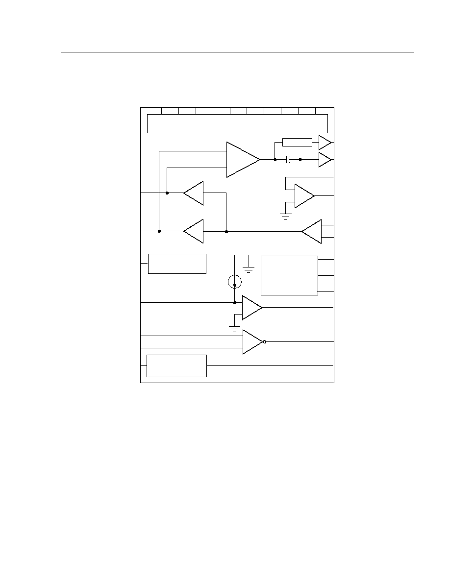
Description
(continued)
12-2569 (C)
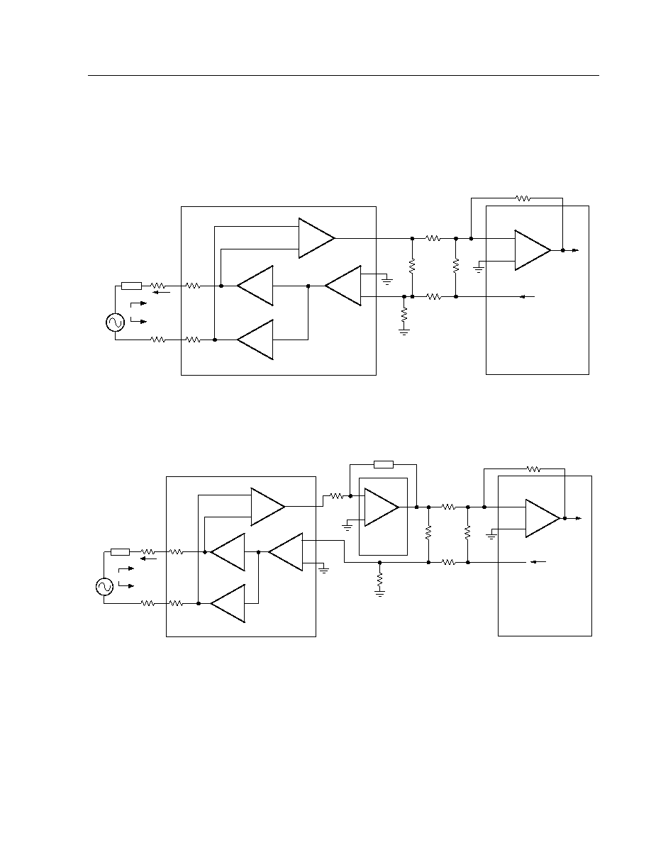
Figure 1. Functional Diagram
B0
B1
+
≠
+
≠
≠1 V/24 mA
≠
+
≠
+
+
≠
A = 4
A = ≠4
POWER CONDITIONING & REFERENCE
PT
PR
dc RESISTANCE
ADJUST
DCR
V
BAT
I
PROG
CF1
BGND
AGND
CF2
ICM
RTSN
RTSP
LCTH
RING GROUND
DETECTOR
RING TRIP DETECTOR
LOOP CLOSURE DETECTOR
BATTERY FEED
STATE CONTROL
SPARE
OP AMP
DCOUT
VITR
RCVP
RCVN
XMT
SN
NLC
RGDET
NRDET
1
B2
FB1
FB2
9.6
V
TX
T
XI
0.1 µF
C
EXTERNAL
3
RECTIFIER
V
REG
V
CC
4
Lucent Technologies Inc.
Data Sheet
March 1997
L7554 Low-Power SLIC
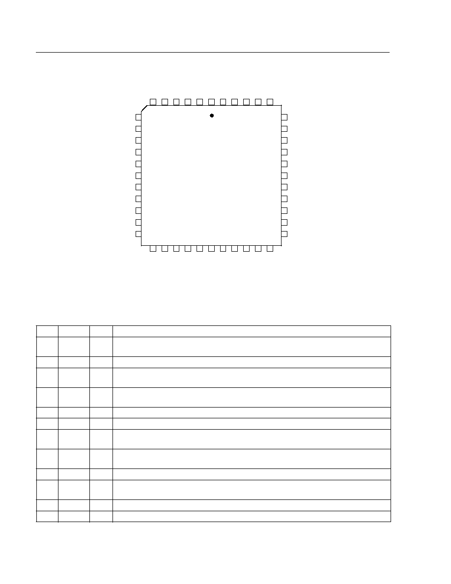
Pin Information
12-2571 (C)
Figure 2. Pin Diagram (PLCC Chip)
Table 1. Pin Descriptions
Pin
Symbol Type
Description
3
I
PROG
I
Current-Limit Program Input.
A resistor to DCOUT sets the dc current limit of the
device.
8
V
CC
--
+5 V Power Supply.
9
RCVP
I
Receive ac Signal Input (Noninverting).
This high-impedance input controls the ac
differential voltage on Tip and Ring.
10
RCVN
I
Receive ac Signal Input (Inverting).
This high-impedance input controls the ac differen-
tial voltage on Tip and Ring.
11
TXI
--
ac/dc Separation.
Connect a 0.1
µ
F capacitor from this pin to VTX
.
12
LCTH
I
Loop Closure Threshold Input.
Connect a resistor to DCOUT to set off-hook threshold.
13
V
REG
I
Regulated Negative dc Battery Voltage.
Can be connected to an external regulator.
Otherwise, connect to V
BAT
.
14
DCOUT
O
dc Output Voltage.
This output is a voltage that is directly proportional to the absolute
value of the differential Tip/Ring current.
15
V
BAT
--
Battery Supply.
Negative high-voltage power supply.
16
PR
I/O
Protected Ring.
The output of the ring driver amplifier and input to loop sensing circuitry.
Connect to loop through overvoltage protection.
18
CF2
--
Filter Capacitor 2.
Connect a 0.1
µ
F capacitor from this pin to AGND.
19
CF1
--
Filter Capacitor 1.
Connect a 0.47
µ
F capacitor from this pin to pin CF2.
I
PROG
NLC
NRDET
RTSP
RTSN
PT
RCVN
RCVP
V
CC
LCTH
V
REG
DCOUT
V
BAT
PR
BGND
DCR
AGND
AGND
B0
I
CM
VITR
CF2
CF1
7
9
10
11
12
13
14
15
16
17
8
6
4
3
2
1
44
43
42
41
40
5
18
20
21
22
23
24
25
26
27
28
19
39
37
36
35
34
33
32
31
30
29
38
FB2
B2
VTX
TXI
B1
XMT
SN
FB1
L7554
R
GDET

Lucent Technologies Inc.
5
Data Sheet
March 1997
L7554 Low-Power SLIC
Pin Information
(continued)
Table 1. Pin Descriptions
(continued)
Pin
Symbol Type
Description
20
VITR
O
Transmit ac Output Voltage.
This output is a voltage that is directly proportional to the
differential ac Tip/Ring current.
21
I
CM
I
Common-Mode Current Sense.
To program ring ground sense threshold, connect a
resistor to V
CC
and connect a capacitor to AGND to filter 50/60 Hz. If unused, the pin can
be left unconnected.
22
R
GDET
O
Ring Ground Detect.
When high, this open-collector output indicates the presence of a
ring ground. To use, connect a 100 k
resistor to V
CC
.
23
B0
I
State Control Input.
B0, B1, and B2 determine the state of the SLIC. See Table 2.
24
AGND
--
Analog Signal Ground
.
25
AGND
--
Analog Signal Ground.
26
DCR
I
dc Resistance for Low Loop Currents.
Leave open for dc feed resistance of 118
, or
short to DCOUT for 618
. Intermediate values can be set by a simple resistor divider
from DCOUT to ground with the tap at DCR.
27
BGND
--
Battery Ground.
Ground return for the battery supply.
29
VTX
O
This output is a voltage that is directly proportional to the differential Tip/Ring current.
30
PT
I/O
Protected Tip
. The output of the tip driver amplifier and input to loop sensing. Connect to
loop through overvoltage protection.
31
RTSN
I
Ring Trip Sense Negative
. Connect this pin to the ringing generator signal through a
high-value resistor.
32
RTSP
I
Ring Trip Sense Positive
. Connect this pin to the ring relay and the ringer series resistor
through a high-value resistor.
33
NRDET
O
Ring Trip Detector Output
. When low, this logic output indicates that ringing is tripped.
34
NLC
O
Loop Detector Output
. When low, this logic output indicates an off-hook condition.
35
B2
I
State Control Input
. B0, B1, and B2 determine the state of the SLIC. See Table 2.
36
B1
I/O
State Control Input
. B0, B1, and B2 determine the state of the SLIC. See Table 2.
37
XMT
O
Transmit ac Output Voltage
. The output of the uncommitted operational amplifier.
38
SN
I
Summing Node
. The inverting input of the uncommitted operational amplifier. A resistor
or network to XMT sets the gain.
39
FB1
I
Forward Battery Slowdown.
A 0.1
µ
F capacitor from FB1 to AGND and from FB2 to
AGND will ramp the polarity reversal transition for added flexibility in applications requiring
quiet polarity reversal. If not needed, the pin can be left open.
40
FB2
I
Forward Battery Slowdown.
A 0.1
µ
F capacitor from FB2 to AGND and from FB1 to
AGND will ramp the polarity reversal transition for added flexibility in applications requiring
quiet polarity reversal. If not needed, the pin can be left open.

6
Lucent Technologies Inc.
Data Sheet
March 1997
L7554 Low-Power SLIC
Functional Description
Table 2. Input State Coding
Table 3. Supervision Coding
Absolute Maximum Ratings
(T
A
= 25
∞
C)
Stresses in excess of the absolute maximum ratings can cause permanent damage to the device. These are abso-
lute stress ratings only. Functional operation of the device is not implied at these or any other conditions in excess
of those given in the operational sections of the data sheet. Exposure to absolute maximum ratings for extended
periods can adversely affect device reliability.
Note: The IC can be damaged unless all ground connections are applied before, and removed after, all other connections. Furthermore, when
powering the device, the user must guarantee that no external potential creates a voltage on any pin of the device that exceeds the
device ratings. Some of the known examples of conditions that cause such potentials during powerup are the following: 1) an inductor
connected to Tip and Ring can force an overvoltage on V
BAT
through the protection devices if the V
BAT
connection chatters, and 2)
inductance in the V
BAT
lead could resonate with the V
BAT
filter capacitor to cause a destructive overvoltage.
B0
B1
B2
State/Definition
1
1
1
Powerup, Forward Battery.
Normal talk and battery feed state. Pin PT is positive with respect to
PR. On-hook transmission is enabled.
1
1
0
Powerup, Reverse Battery.
Normal talk and battery feed state. Pin PR is positive with respect to
PT. On-hook transmission is enabled.
0
1
1
Ground Start.
Tip drive amplifier is turned off. The device presents a high-impedance (>100 k
)
to the PT pin and a current-limited battery to the PR pin. Output pin RGDET indicates current flow-
ing in the ring lead.
0
1
0
Low-Power Scan, Reverse Battery.
Except for off-hook supervision, all circuits are shut down to
conserve power. Pin PR is positive with respect to PT. On-hook transmission is disabled.
0
0
1
Low-Power Scan, Forward Battery.
Except for off-hook supervision, all circuits are shut down to
conserve power. Pin PT is positive with respect to PR. On-hook transmission is disabled.
0
0
0
Disconnect.
The Tip and Ring amplifiers are turned off and the SLIC goes to a high-impedance
state (>100 k
).
Pin NLC
Pin NRDET
Pin RGDET
0 = off-hook
1 = on-hook
0 = ring trip
1 = no ring trip
1 = ring ground
0 = no ring ground
Parameter
Symbol
Value
Unit
5 V Power Supply
V
CC
7.0
V
Battery (Talking) Supply
V
BAT
≠75
V
Logic Input Voltage
--
≠0.5 to +7.0
V
Analog Input Voltage
--
≠7.0 to +7.0
V
Maximum Junction Temperature
T
J
165
∞
C
Storage Temperature Range
T
stg
≠40 to +125
∞
C
Relative Humidity Range
R
H
5 to 95
%
Ground Potential Difference (BGND to AGND)
--
±
3
V
PT or PR Fault Voltage (dc)
V
PT
, V
PR
(V
BAT
≠ 5) to +3
V
PT or PR Fault Voltage (10 x 1000
µ
s)
V
PT
, V
PR
(V
BAT
≠ 15) to +15
V
Current into Ring Trip Inputs
I
RTSP
, I
RTSN
±
240
µ
A

Lucent Technologies Inc.
7
Data Sheet
March 1997
L7554 Low-Power SLIC
Recommended Operating Conditions
Electrical Characteristics
Minimum and maximum values are testing requirements. Typical values are characteristic of the device and are the
result of engineering evaluations. Typical values are for information purposes only and are not part of the testing
requirements. Minimum and maximum values apply across the entire temperature range (≠40
∞
C to +85
∞
C) and
the entire battery range unless otherwise specified. Typical is defined as 25
∞
C, V
CC
= 5.0 V, V
BAT
= ≠48 V, and
I
LIM
= 40 mA. Positive currents flow into the device. Test circuit is Figure 4 unless noted.
Table 4. Power Supply
1. This parameter is not tested in production. It is guaranteed by design and device characterization.
Parameter
Min
Typ
Max
Unit
Ambient Temperature
≠40
--
85
∞
C
V
CC
Supply Voltage
4.75
5.0
5.25
V
V
BAT
Supply Voltage:
L7554AP
L7554BP
≠24
≠24
≠40
≠48
≠60
≠72
V
V
Loop Closure Threshold-detection Programming Range
--
10
I
LIM
mA
dc Loop Current-limit Programming Range
5
40
45
mA
On- and Off-hook 2-wire Signal Level
--
1
2.2
Vrms
ac Termination Impedance Programming Range
150
600
1300
Parameter
Min
Typ
Max
Unit
Power Supply--Powerup, No Loop Current
I
CC
I
BAT
(V
BAT
= ≠48 V)
Power Dissipation (V
BAT
= ≠48 V)
--
--
--
4.1
≠3.0
165
4.8
≠3.5
191
mA
mA
mW
Power Supply--Low-Power Scan, Forward Bat, No Loop
Current
I
CC
I
BAT
(V
BAT
= ≠48 V)
Power Dissipation (V
BAT
= ≠48 V)
--
--
--
2.7
≠1.4
82
3.7
≠1.7
100
mA
mA
mW
Power Supply Rejection 500 Hz to 3 kHz
(See Figures 5, 6, 15, and 16.)
1
V
CC
V
BAT
35
45
--
--
--
--
dB
dB
Thermal Protection Shutdown (T
jc
)
--
175
--
∞
C
Thermal Resistance, Junction to Ambient (
JA
)
--
47
--
∞
C/W

8
Lucent Technologies Inc.
Data Sheet
March 1997
L7554 Low-Power SLIC
Electrical Characteristics
(continued)
Table 5. 2-Wire Port
1. The longitudinal current is independent of dc loop current.
2. Current-limit I
LIM
is programmed by a resistor, R
PROG
, from pin I
PROG
to DCOUT. I
LIM
is specified at the loop resistance where current limiting
begins (see Figure 25). Select R
PROG
(k
) = 1.67 x I
LIM
(mA).
3.
IEEE is a registered trademark of The Institute of Electrical and Electronics Engineers, Inc.
4. Longitudinal balance of circuit card will depend on loop series resistance matching (see Figures 23 and 24).
5. This parameter is not tested in production. It is guaranteed by design and device characterization.
Parameter
Min
Typ
Max
Unit
Tip or Ring Drive Current
= dc + Longitudinal + Signal Currents
65
--
--
mA
Signal Current
15
--
--
mArms
Longitudinal Current Capability per Wire
1
8.5
15
--
mArms
dc Loop Current Limit
2
R
LOOP
= 100
Programmability Range
Accuracy (20 mA < I
LIM
< 40 mA)
--
5
--
I
LIM
--
--
--
45
±
12
mA
mA
%
Powerup Open Loop Voltage Levels
Common-mode Voltage
Differential Voltage:
V
BAT
= ≠48 V, Temperature = 25
∞
C
V
BAT
= ≠72 V, Temperature = 85
∞
C (L7554BP)
--
|V
BAT
+ 7.0|
|V
BAT
+ 10.0|
V
BAT
/2
|V
BAT
+ 6.5|
|V
BAT
+ 6.8|
--
|V
BAT
+ 6.0|
--
V
V
V
Disconnect State
PT Resistance (V
BAT
< V
PT
< 0 V)
PR Resistance (V
BAT
< V
PR
< 0 V)
100
100
143
133
--
--
k
k
Ground Start State
PT Resistance
100
143
--
k
dc Feed Resistance (for I
LOOP
below regulation level)
90
113
133
Loop Resistance Range (≠3.17 dBm overload into
600
; not including protection)
I
LOOP
= 20 mA at V
BAT
= ≠48 V
I
LOOP
= 20 mA at V
BAT
= ≠24 V
1900
700
--
--
--
--
Longitudinal to Metallic Balance--
IEEE
3
Std. 455
(See Figure 7.)
4
50 Hz to 1 kHz
1 kHz to 3 kHz
64
60
75
70
--
--
dB
dB
Metallic to Longitudinal Balance
200 Hz to 4 kHz
46
--
--
dB
RFI Rejection (See Figure 8.)
5
0.5 Vrms, 50
Source, 30% AM Mod. 1 kHz
500 kHz to 100 MHz
--
≠55
≠45
dBV

Lucent Technologies Inc.
9
Data Sheet
March 1997
L7554 Low-Power SLIC
Electrical Characteristics
(continued)
Table 6. Analog Pin Characteristics
1. Loop closure threshold is programmed by resistor R
LCTH
from pin LCTH to pin DCOUT.
2. Ring ground threshold is programmed by resistor R
ICM2
from pin I
CM
to V
CC
.
Table 7. Uncommitted Op Amp Characteristics
Parameter
Min
Typ
Max
Unit
Differential PT/PR Current Sense (DCOUT)
Gain (PT/PR to DCOUT)
Offset Voltage @ I
LOOP
= 0, V
BAT
= ≠48 V
≠119
≠200
≠125
--
≠127
200
V/A
mV
Loop Closure Detector Threshold
1
Programming Accuracy
--
--
±
20
%
Ring Ground Detector Threshold
2
R
ICM
= 83 k
Programming Accuracy
3
--
6
--
10
±
25
k
%
Ring Trip Comparator
Input Offset Voltage
--
--
±
10
mV
RCVN, RCVP
Input Bias Current
--
≠0.2
≠1
µ
A
Parameter
Min
Typ
Max
Unit
Input Offset Voltage
Input Offset Current
Input Bias Current
Differential Input Resistance
--
--
--
--
±
5
±
10
200
1.5
--
--
--
--
mV
nA
nA
M
Output Voltage Swing (R
L
= 10 k
)
Output Resistance (A
VCL
= 1)
--
--
±
3.5
2.0
--
--
Vpk
Small Signal GBW
--
700
--
kHz

10
Lucent Technologies Inc.
Data Sheet
March 1997
L7554 Low-Power SLIC
Electrical Characteristics
(continued)
Table 8. ac Feed Characteristics
1. Set by external components. Any complex impedance R
1
+ R2 || C between 150
and 1300
can be synthesized.
2. This parameter is not tested in production. It is guaranteed by design and device characterization.
3. Return loss and transhybrid loss are functions of device gain accuracies and the external hybrid circuit. Guaranteed performance assumes
1% tolerance of external components.
Parameter
Min
Typ
Max
Unit
ac Termination Impedance
1
150
--
1300
Longitudinal Impedance
2
--
40
46
Total Harmonic Distortion--200 Hz to 4 kHz
2
Off-hook
On-hook
--
--
--
--
0.3
1.0
%
%
Transmit Gain, f = 1 kHz (PT/PR to VITR)
Transmit Accuracy in dB, 25
∞
C
Transmit Accuracy in dB, Full Temperature Range
--
≠0.15
≠0.22
≠400
0
0
--
0.15
0.22
V/A
dB
dB
Receive + Gain, f = 1 kHz (RCVP to PT/PR)
Receive ≠ Gain, f = 1 kHz (RCVN to PT/PR)
Receive Accuracy in dB, 25
∞
C
Receive Accuracy in dB, Full Temperature Range
--
--
≠0.18
≠0.25
8.00
≠8.00
0
0
--
--
0.18
0.25
≠
≠
dB
dB
Gain vs. Frequency (transmit and receive)
(600
termination; reference 1 kHz
2
)
200 Hz to 300 Hz
300 Hz to 3.4 kHz
3.4 kHz to 16 kHz
16 kHz to 266 kHz
≠1.00
≠0.3
≠0.5
--
0.0
0.0
≠0.1
--
0.05
0.05
0.3
2.0
dB
dB
dB
dB
Gain vs. Level (transmit and receive)(reference 0 dBV
2
)
≠50 dB to +3 dB
≠0.05
0
0.05
dB
Return Loss
3
200 Hz to 500 Hz
500 Hz to 3400 Hz
20
26
24
29
--
--
dB
dB
2-wire Idle-channel Noise (600
termination)
Psophometric
C-message
3 kHz Flat
--
--
--
≠87
2
10
≠77
12
20
dBmp
dBrnC
dBrn
Transmit Idle-channel Noise
Psophometric
C-message
3 kHz flat
--
--
--
≠82
7
15
≠77
12
20
dBmp
dBrnC
dBrn
Transhybrid Loss
3
200 Hz to 500 Hz
500 Hz to 3400 Hz
21
26
24
29
--
--
dB
dB

Data Sheet
March 1997
Lucent Technologies Inc.
11
L7554 Low-Power SLIC
Electrical Characteristics
(continued)
Table 9. Logic Inputs and Outputs
All outputs except RGDET are open-collector with internal pull-up resistor. RGDET is open-collector without inter-
nal pull-up.
Parameter
Symbol
Min
Typ
Max
Unit
Input Voltages
Low Level (permissible range)
High Level (permissible range)
V
IL
V
IH
≠0.5
2.0
0.4
2.4
0.7
V
CC
V
V
Input Currents
Low Level (V
CC
= 5.25 V, V
I
= 0.4 V)
High Level (V
CC
= 5.25 V, V
I
= 2.4 V)
I
IL
I
IH
--
--
≠115
≠60
≠200
≠100
µ
A
µ
A
Output Voltages (open-collector with internal pull-up
resistor)
Low Level (V
CC
= 4.75 V, I
OL
= 360
µ
A)
High Level (V
CC
= 4.75 V, I
OH
= ≠20
µ
A)
V
OL
V
OH
0
2.4
0.2
--
0.4
V
CC
V
V
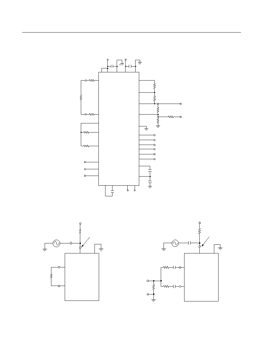
Ring Trip Requirements
s
Ringing signal:
-- Voltage, minimum 35 Vrms, maximum 100 Vrms.
-- Frequency, 17 Hz to 23 Hz.
-- Crest factor, 1.4 to 2.
s
Ringing trip:
--
100 ms (typical),
250 ms (V
BAT
= ≠33 V, loop
length = 530
).
s
Pretrip:
-- The circuits in Figure 3 will not cause ringing trip.
12-2572 (C)
Figure 3. Ring Trip Circuits
RING
RING
RING
100
10 k
6 µF
TIP
TIP
TIP
2 µF
200
SWITCH CLOSES < 12 ms
12
Lucent Technologies Inc.
Data Sheet
March 1997
L7554 Low-Power SLIC
Test Configurations
12-2570 (C)
Figure 4. L7554 Basic Test Circuit
B1
NLC
V
BAT
V
BAT
BGND V
CC
AGND
V
CC
0.1 µF
0.1 µF
PT
PR
I
PROG
DCOUT
LCTH
RTSP
RTSN
I
CM
VTR
SN
RCVP
B0
CF1
20 k
20 k
V
REG
XMT
RCVN
NRDET
RGDET
0.1 µF
CF2
R
LOOP
XMT
65 k
10 k
RCV
68.1 k
24.9 k
L7554
SLIC
26 k
VTX
TXI
FB2 FB1
0.1 µF
B2
0.1 µF
100
100
PSRR = 20 log
12-2335.a (C)
Figure 5. Metallic PSRR
PSRR = 20 log
12-2336.a (C)
Figure 6. Longitudinal PSRR
4.7 µF
100
V
BAT
OR
V
CC
DISCONNECT
BYPASS CAP
V
T/R
900
V
BAT
OR V
CC
TP
PR
BASIC
TEST CIRCUIT
+
≠
V
S
V
S
V
T/R
----------
V
S
4.7 µF
100
V
BAT
OR
V
CC
DISCONNECT
BYPASS CAP
56.3
V
BAT
OR V
CC
PT
PR
BASIC
TEST CIRCUIT
67.5
10 µF
10 µF
67.5
V
M
+
≠
V
S
V
M
-------
Data Sheet
March 1997
Lucent Technologies Inc.
13
L7554 Low-Power SLIC
Test Configurations
(continued)
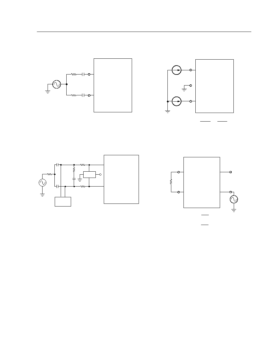
LONGITUDINAL BALANCE = 20 log
12-2584 (C)
Figure 7. Longitudinal Balance
12-2586 (C)
Figure 8. RFI Rejection
12-2585 (C)
Figure 9. Longitudinal Impedance
12-2587 (C)
Figure 10. ac Gains
PT
PR
BASIC
TEST CIRCUIT
368
100 µF
100 µF
368
V
M
+
≠
V
S
V
S
V
M
-------
BASIC
TEST CIRCUIT
V
S
= 0.5 Vrms 30% AM 1 kHz MODULATION,
f = 500 kHz≠≠1 MHz
DEVICE IN POWERUP MODE, 600
TERMINATION
PT
PR
V
BAT
0.01 µF
0.01 µF
600
2.15
µF
82.5
82.5
HP4935A
TIMS
50
1
2
4
6,7
V
S
LB1201
PT
PR
BASIC
TEST CIRCUIT
+
≠
+
≠
I
LONG
I
LONG
V
PT
V
PR
Z
LONG
=
OR
V
PT
I
LONG
V
PR
I
LONG
PT
PR
BASIC
TEST CIRCUIT
600
V
T/R
+
≠
G
XMT
=
V
XMT
V
T/R
G
RCV
=
V
T/R
V
RCV
XMT
RCV
V
S

14
Lucent Technologies Inc.
Data Sheet
March 1997
L7554 Low-Power SLIC
Applications
12-2573 (C)
Figure 11. Basic Loop Start Application Circuit Using T7513 Type Codec
12-2821 (C)
Figure 12. Ground Start Application Circuit
R
PROG
66.8 k
R
LCTH
24.9 k
TIP R
PT
20
RING
250 V PROT
R
PR
L7581
RELAY
PT
30
0.1 µF
C
CC
14
DCOUT
3
12
LCTH
V
CC
8
V
CC
20
PR
16
RTSP
32
R
TS1
402
C
RTS2
0.27 µF
RTSN
31
R
TS2
274 k
R
TSN
2.0 M
V
RING
V
BAT
CF2
18
CF1
19
C
F1
0.47 µF
AGND
24
AGND
25
BGND
27
I
PROG
V
BAT
15
C
BAT
0.1 µF
VITR
RCVP
RCVN
20
9
10
R
GP
20.0 k
R
T1
86.6 k
R
T2
18.7 k
R
RCV
48.7 k
R
HB1
28.0 k
VFXIN
VFXIP
R
X
28.0 k
GSX
PWROP
PWRON
GSR
DX
DR
FSX
FSR
MC
PD
CLKSEL
A/µ
T7513
CODEC
CONTROL
INPUTS
PCM
HIGHWAY
SYNCH
AND
CLOCK
≠
+
L7554
SLIC
B1
B0
36
23
CONTROL
INPUTS
NLC
NRDET
34
33
SUPERVISION
OUTPUTS
C
RTS1
0.022 µF
TXI
V
TX
CB2
0.1 µF
29
11
B2 35
R
TSP
2.0 M
C
GP
330 pF
C
F2
0.1 µF
V
BAT
V
REG
V
CC
RGDET
100 k
RGDET
ICM
0.47 µF
CICM
LOOP START
APPLICATION CIRCUIT
22
21
82.5 k
RICM2

Lucent Technologies Inc.
15
Data Sheet
March 1997
L7554 Low-Power SLIC
Applications
(continued)
Table 10. Parts List for Loop Start and Ground Start Applications
Name
Value
Function
Integrated Circuits
SLIC
L7554
Subscriber loop interface circuit (SLIC).
Protector
250 V Thyristor type
Secondary protection.
Ringing Relay
L7581
Switches ringing signals.
Codec
T7513
First-generation codec.
Overvoltage Protection
R
PT
20
, Fusible
Protection resistor.
R
PR
20
, Fusible
Protection resistor.
Power Supply
C
BAT1
0.1
µ
F, 20%, 100 V
V
BAT
filter capacitor.
C
CC
0.1
µ
F, 20%, 10 V
V
CC
filter.
C
F1
0.47
µ
F, 20%, 100 V
With C
F2
, improves idle channel noise.
C
F2
0.1
µ
F, 20%, 100 V
With C
F1
, improves idle channel noise.
dc Profile
R
PROG
66.8 k
, 1%, 1/4 W
Sets dc loop current limit.
ac Characteristics
C
B2
0.1
µ
F, 20%, 100 V
ac/dc separation capacitor.
C
GB
330
µ
F, 20%, 10 V
Loop stability.
R
T1
86.6 k
, 1%, 1/4 W
With R
GP
and R
RCV
, sets ac termination impedance.
R
RCV
48.7 k
, 1%, 1/4 W
With R
GP
and R
T1
, sets receive gain.
R
GP
20.0 k
, 1%, 1/4 W
With R
T1
and R
RCV
, sets ac termination impedance
and receive gain.
C
GP
330 pF, 10 V, 20%
Loop stability.
R
T2
18.7 k
, 1%, 1/4 W
With R
X
, sets transmit gain in codec.
R
X
28.0 k
, 1%, 1/4 W
With R
T2
, sets transmit gain in codec.
R
HB1
28.0 k
, 1%, 1/4 W
Sets hybrid balance.
Supervision
R
LCTH
24.9 k
, 1%, 1/4 W
Sets loop closure (off-hook) threshold.
R
TS1
402
, 5%, 2 W
Ringing source series resistor.
R
TS2
274 k
, 5%, 1/4 W
With C
RTS2
, forms first pole of a double pole,
2 Hz ring trip sense filter.
C
RTS1
0.022
µ
F, 20%, 5 V
With R
TSN
, R
TSP
, forms second 2 Hz filter pole.
C
RTS2
0.27
µ
F, 20%, 100 V
With R
TS2
, forms first 2 Hz filter pole.
R
TSN
2 M
, 5%, 1/4 W
With C
RTS1
, R
TSP
, forms second 2 Hz filter pole.
R
TSP
2 M
, 5%, 1/4 W
With C
RTS1
, R
TSN
, forms second 2 Hz filter pole.
Ground Start
C
ICM
0.47
µ
F, 20%, 10 V
Provides 60 Hz filtering for ring ground detection.
R
GDET
100 k
, 20%, 1/4 W
Digital output pull-up resistor.
R
ICM2
82.5 k
, 1%, 1/4 W
Sets ring ground detection threshold.

16
Lucent Technologies Inc.
Data Sheet
March 1997
L7554 Low-Power SLIC
Applications
(continued)
Design Considerations
Table 11 shows the design parameters of the application circuit shown in Figure 11. Components that are adjusted
to program these values are also shown.
Table 11. 600
Design Parameters
Design Parameter
Parameter Value
Components Adjusted
Loop Closure Threshold
10 mA
R
LCTH
dc Loop Current Limit
40 mA
R
PROG
dc Feed Resistance
183
R
PT
, R
PR
2-wire Signal Overload Level
3.14 dBm
--
ac Termination Impedance
600
R
T1
, R
GP
, R
RCV
Hybrid Balance Line Impedance
600
R
HB1
Transmit Gain
0 dB
R
T2
, R
X
Receive Gain
0 dB
R
RCV
, R
GP
, R
T1
Data Sheet
March 1997
Lucent Technologies Inc.
17
L7554 Low-Power SLIC
Applications
(continued)
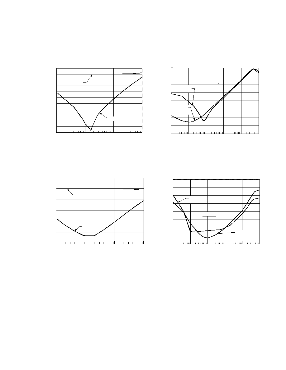
Characteristic Curves
12-2828 (C)
Figure 13. 7551 Receive Gain and Hybrid Balance
vs. Frequency
12-2829 (C)
Figure 14. 7551 Transmit Gain and Return Loss vs.
Frequency
12-2830 (C)
Figure 15. 7551 Typical V
CC
Power Supply Rejection
12-2871 (C)
Figure 16. 7551 Typical V
BAT
Power Supply
Rejection
FREQUENCY (Hz)
100
10
5
≠20
≠10
0
10
4
≠50
≠40
≠30
RECEIVE GAIN
1000
HYBRID BALANCE
(dB)
100
1000
10
4
10
5
≠50
≠30
≠20
≠10
0
FREQUENCY (Hz)
≠40
TRANSMIT GAIN
RETURN LOSS
(dB)
10
100
10
5
10
6
≠80
≠70
≠20
≠10
0
FREQUENCY (Hz)
1000
10
4
≠50
≠40
≠60
≠30
PSRR (dB)
CURRENT
LIMIT
BELOW
CURRENT
LIMIT
SPEC.
10
100
10
5
10
6
≠80
≠70
≠20
≠10
0
FREQUENCY (Hz)
1000
10
4
≠50
≠40
≠60
≠30
PSRR (dB)
BELOW
CURRENT
LIMIT
SPECIFICATION RANGE
CURRENT
LIMIT

18
Lucent Technologies Inc.
Data Sheet
March 1997
L7554 Low-Power SLIC
Applications
(continued)
Characteristic Curves
(continued)
Note: V
BAT
= ≠48 V.
12-3015 (C)
Figure 17. Loop Closure Program Resistor
Selection
Note: Tip lead is open; V
BAT
= ≠48 V.
12-3016 (C)
Figure 18. Ring Ground Detection Programming
Note: V
BAT
= ≠48 V; I
LIM
= 22 mA; R
DC1
= 113
.
12-3050 (C)
Figure 19. Loop Current vs. Loop Voltage
Note: V
BAT
= ≠48 V; I
LIM
= 22 mA; R
DC1
= 113
.
12-3051 (C)
Figure 20. Loop Current vs. Loop Resistance
0
5
20
25
0
10
20
30
60
LOOP CLOSURE THRESHOLD RESISTOR, R
LCTH
(k
)
50
15
10
40
OFF-HOOK THRESHOLD LOOP CURRENT
(mA)
AMBIENT TEMPERATURE, T
A
(
∞
C)
20
40
60
140
180
0
500
1000
1500
2000
80
100
120
160
STILL AIR
47
∞
C/W
300 cu. ft./ min.
36
∞
C/W
POWER (mW)
LOOP CURRENT (mA)
0
10
20
50
0
20
30
40
50
LOOP VOLTAGE (V)
30
40
10
1
10 k
I
LIM
≠1
R
DC1
LOOP RESISTANCE, R
LOOP
(
)
0
500
1000
2000
0
20
30
40
50
1500
10
LOOP CURRENT (mA)

Data Sheet
March 1997
Lucent Technologies Inc.
19
L7554 Low-Power SLIC
Applications
(continued)
Characteristic Curves
(continued)
Note: V
BAT
= ≠48 V; I
LIM
= 22 mA; R
DC1
= 113
.
12-3052 (C)
Figure 21. 7551 Typical SLIC Power Dissipation vs.
Loop Resistance
12-2825 (C)
Figure 22. Power Derating
12-3019 (C)
Figure 23. Longitudinal Balance Resistor Mismatch
Requirements
12-3021 (C)
Figure 24. Longitudinal Balance vs. Protection
Resistor Mismatch
LOOP RESISTANCE, R
LOOP
(
)
0
500
1000
2000
0
1000
1500
1500
500
SLIC POWER DISSIPATION (mW)
AMBIENT TEMPERATURE, T
A
(
∞
C)
20
40
60
140
180
0
500
1000
1500
2000
80
100
120
160
STILL AIR
47
∞
C/W
300 cu. ft./ min.
36
∞
C/W
POWER (mW)
0
8
0
20
60
100
120
PROTECTION RESISTOR VALUE (
)
7
6
5
4
3
2
1
40
80
49 dB, RP MATCHED TO 1.5
58 dB, RP MATCHED
TO 0.5
PROTECTION RESISTOR MISMATCH (%)
40
60
0.0
0.5
1.5
2.5
PROTECTION RESISTOR MISMATCH (
)
55
50
45
1.0
2.0
LONGITUDINAL BALANCE (dB)
20
20
Lucent Technologies Inc.
Data Sheet
March 1997
L7554 Low-Power SLIC
Applications
(continued)
dc Applications
Battery Feed
The dc feed characteristic can be described by:
where:
I
L
= dc loop current.
V
T/R
= dc loop voltage.
|V
BAT
| = battery voltage magnitude.
V
OH
= overhead voltage. This is the difference between
the battery voltage and the open loop Tip/Ring
voltage.
R
L
= loop resistance, not including protection resistors.
R
P
= protection resistor value.
Rdc = SLIC internal dc feed resistance.
The design begins by drawing the desired dc template.
An example is shown in Figure 25.
Note: V
BAT
= ≠48 V; I
LIM
= 22 mA; R
DC1
= 113
.
12-3050 (C)
Figure 25. Loop Current vs. Loop Voltage
Starting from the on-hook condition and going through
to a short circuit, the curve passes through two regions:
Region 1; On-hook and low loop currents. The slope
corresponds to the dc resistance of the SLIC, R
DC1
(de-
fault is 113
typical). The open-circuit voltage is the
battery voltage less the overhead voltage of the device,
V
OH
(default is 6.5 V typical). These values are suitable
for most applications, but can be adjusted if needed. For
more information, see the sections entitled Adjusting dc
Feed Resistance and Adjusting Overhead Voltage.
Region 2; Current limit. The dc current is limited to a val-
ue determined by external resistor R
PROG
. This region of
the dc template has a high resistance (10 k
).
Calculate the external resistor as follows:
R
PROG
(k
) = 1.67 I
LIM
(mA)
Overhead Voltage
In order to drive an on-hook ac signal, the SLIC must
set up the Tip and Ring voltage to a value less than the
battery voltage. The amount that the open loop voltage
is decreased relative to the battery is referred to as the
overhead voltage. Expressed as an equation,
V
OH
= |V
BAT
| ≠ (V
PT
≠ V
PR
)
Without this buffer voltage, amplifier saturation will
occur and the signal will be clipped. The 7551 is auto-
matically set at the factory to allow undistorted on-hook
transmission of a 3.17 dBm signal into a 900
loop
impedance. For applications where higher signal levels
are needed, e.g., periodic pulse metering, the 2-wire
port of the SLIC can be programmed with pin DCR.
The drive amplifiers are capable of 4 Vrms minimum
(V
AMP
). Referring to Figure 26, the internal resistance
has a worst-case value of 46
. So, the maximum sig-
nal the device can guarantee is:
Thus, R
P
35
allows 2.2 Vrms metering signals. The
next step is to determine the amount of overhead volt-
age needed. The peak voltage at output of Tip and
Ring amplifiers is related to the peak signal voltage by:
V
T R
/
V
B A T
V
O H
≠
(
)
R
L
◊
R
L
2R
P
Rdc
+
+
--------------------------------------------
=
I
L
V
B A T
V
O H
≠
R
L
2R
P
Rdc
+
+
-----------------------------------
=
LOOP CURRENT (mA)
0
10
20
50
0
20
30
40
50
LOOP VOLTAGE (V)
30
40
10
1
10 k
I
LIM
≠1
R
DC1
V
T/R
4 V
Z
T/R
Z
T/R
2 R
P
46
+
(
)
+
-----------------------------------------
=
vamp = v
T/R
1
2 R
P
40
+
(
)
Z
T R
/
------------------------------
+

Lucent Technologies Inc.
21
Data Sheet
March 1997
L7554 Low-Power SLIC
Applications
(continued)
dc Applications
(continued)
12-2563 (C)
Figure 26. SLIC 2-Wire Output Stage
In addition to the required peak signal level, the SLIC
needs about 2 V from each power supply to bias the
amplifier circuitry. It can be thought of as an internal
saturation voltage. Combining the saturation voltage
and the peak signal level, the required overhead can be
expressed as:
where V
SAT
is the combined internal saturation voltage
between the Tip/Ring amplifiers and V
SAT
(4.0 V typ.).
R
P
(
) is the protection resistor value, and 40
is the
output series resistance of each internal amplifier.
Z
T/R
(
) is the ac loop impedance.
Example 1, On-hook Transmission of a Meter Pulse:
Signal level: 2.2 Vrms into 200
35
protection resistors
I
LOOP
= 0 (on-hook transmission of the metering
signal)
Accounting for V
SAT
tolerance of 0.5 V, a nominal
overhead of 9.9 V would ensure transmission of an
undistorted 2.2 V metering signal.
Adjusting Overhead Voltage
To adjust the open loop 2-wire voltage, pin DCR is
programmed at the midpoint of a resistive divider from
ground to either ≠5 V or V
BAT
. In the case of ≠5 V, the
overhead voltage will be independent of the battery
voltage. Figure 27 shows the equivalent input circuit to
adjust the overhead.
12-2562 (C)
Figure 27. Equivalent Circuit for Adjusting the
Overhead Voltage
The overhead voltage is programmed by using the fol-
lowing equation:
V
OH
= 6.5 ≠ 4 V
DCR
≠
V
T/R
[Z
T/R
]
V
AMP
+
≠
R
OC
/2
R
P
R
P
+
R
OC
/2
V
O H
V
S A T
1
2 R
P
40
+
(
)
Z
T R
/
------------------------------
+
v
T R
/
+
=
V
S A T
1
2 R
P
40
+
(
)
Z
T R
/
------------------------------
+
2 Z
T R
/
1000
----------------
10
dBm 20
/
◊
+
=
V
OH
4.0
1
2 35
40
+
(
)
200
----------------------------
+
2 2.2
( )
+
=
9.4 V
=
DCR
25 k
±
30%
R1
R2
≠5 V
6.5
4
5
R
1
25 k
||
R
2
R
1
25 k
||
+
--------------------------------------
◊
≠
≠
=
6.5
20
R
1
25 k
||
R
2
R
1
25 k
||
+
--------------------------------------
+
=
22
22
Lucent Technologies Inc.
Data Sheet
March 1997
L7554 Low-Power SLIC
Applications
(continued)
dc Applications
(continued)
Adjusting dc Feed Resistance
The dc feed resistance may be adjusted with the help of
Figure 28.
12-2560 (C)
Figure 28. Equivalent Circuit for Adjusting the dc
Feed Resistance
Adjusting Overhead Voltage and dc Feed
Resistance Simultaneously
The following paragraphs describe the independent set-
ting of the overhead voltage and the dc feed resistance.
If both need to be set to customized values, combine
the two circuits as shown in Figure 29.
12-2561 (C)
Figure 29. Adjusting Both Overhead Voltage and dc
Feed Resistance
This is an equivalent circuit for adjusting both the dc
feed resistance and overhead voltage together.
The adjustments can be made by the simple superposi-
tion of the overhead and dc feed equations:
When selecting external components, select R1 on the
order of 5 k
to minimize the programming inaccuracy
caused by the internal 25 k
resistor. Lower values can
be used; the only disadvantage is the power consump-
tion of the external resistors.
Loop Range
The equation below can be rearranged to provide the
loop range for a required loop current:
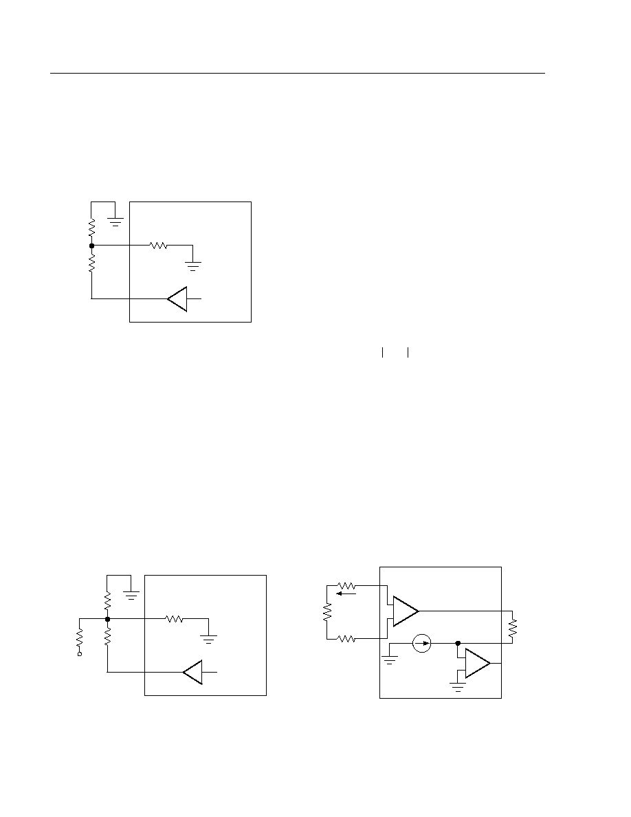
Off-Hook Detection
The loop closure comparator has built-in longitudinal
rejection, eliminating the need for an external 60 Hz fil-
ter. This applies in both powerup and low-power scan
states. The loop-closure detection threshold is set by
resistor R
LCTH
. Referring to Figure 30, NLC is high in an
on-hook condition (I
TR
= 0, V
DCOUT
= 0), and
V
LCTH
= 0.05 mA x
R
LCTH
. The off-hook comparator
goes low when V
LCTH
crosses zero and then goes neg-
ative:
V
LCTH
= 0.05 mA x R
LCTH
+ V
DCOUT
= 0.05 x R
LCTH
≠ 0.125 V/mA x I
TR
R
LCTH
(k
) = 2.5 x I
TR
(mA)
12-2553.a (C)
Figure 30. Off-Hook Detection Circuit
DCR
25 k
±
30%
R1
R3
DCOUT
Rdc
113
500
V
D C R
V
D C O U T
--------------------
+
=
113
500
R
1
25 k
||
R
3
R
1
25 k
||
+
----------------------------------
+
=
DCR
25 k
±
30%
R1
R3
DCOUT
R2
≠5 V
V
O H
6.5
20
R
1
25 k
R
3
||
||
R
2
R
1
25 k
R
3
||
||
+
----------------------------------------------
+
=
Rdc
113
500
R
1
25 k
||
R
3
R
1
25 k
||
+
-----------------------------------
+
=
R
L
V
B A T
V
O H
≠
I
L
----------------------------
2R
P
≠
Rdc
≠
=
R
L
ITR
R
P
R
P
PR
≠
+
≠
+
DCOUT
R
LCTH
LCTH
NLC
PT
≠0.125 V/mA
0.05 mA
Lucent Technologies Inc.
23
Data Sheet
March 1997
L7554 Low-Power SLIC
Applications
(continued)
dc Applications
(continued)
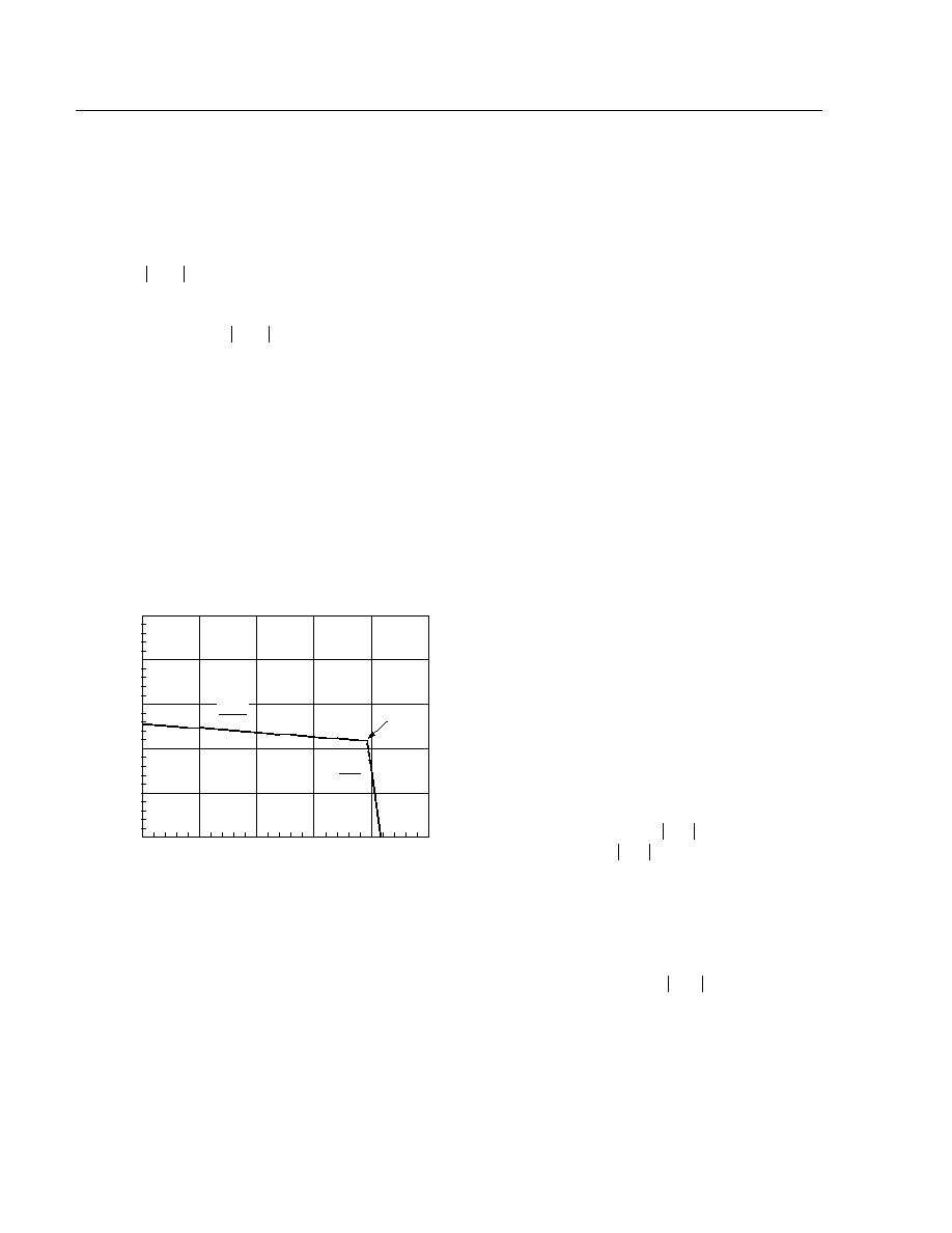
Ring Trip Detection
The ring trip circuit is a comparator that has a special in-
put section optimized for this application. The equiva-
lent circuit is shown in Figure 31, along with its use in an
application using unbalanced, battery-backed ringing.
12-3014 (C)
Figure 31. Ring Trip Equivalent Circuit and
Equivalent Application
The comparator input voltage compliance is V
CC
to
V
BAT
, and the maximum current is 240
µ
A in either
direction. Its application is straightforward. A resistance
(R
TSN
+ R
TS2
) in series with the R
TSN
input establishes a
current that is repeated in the R
TSP
input. A slightly
lower resistance (R
TSP
) is placed in series with the R
TSP
input. When ringing is being injected, no dc current
flows through R
TS1
, so the R
TSP
input is at a lower
potential than R
TSN
. When enough dc loop current
flows, the R
TSP
input voltage increases to trip the com-
parator. In Figure 31, a low-pass filter with a double
pole at 2 Hz was implemented to prevent false ring trip.
The following example illustrates how the detection cir-
cuit of Figure 31 will trip at 12.5 mA dc loop current us-
ing a ≠48 V battery.
The current I
N
is repeated as I
P
in the positive compar-
ator input. The voltage at comparator input R
TSP
is:
Using this equation and the values in the example, the
voltage at input R
TSP
is ≠12 V during ringing injection
(I
LOOP(dc)
= 0). Input R
TSP
is, therefore, at a level of 5 V
below R
TSN
. When enough dc loop current flows
through R
TS1
to raise its dc drop to 5 V, the comparator
will trip. In this example,
Ring Ground Detection
Pin ICM sinks a current proportional to the longitudinal
loop current. It is also connected to an internal compar-
ator whose output is pin RGDET. In a ground start
application where Tip is open, the ring ground current
is half differential and half common mode. In this case,
to set the ring ground current threshold, connect a
resistor R
ICM
from pin ICM to V
CC
. Select the resistor
according to the following relation:
The above equation is shown graphically in Figure 18.
It applies for the case of Tip open. The more general
equation can be used in ground key application to
detect a common-mode current I
CM
:
+
≠
R
TSP
R
LOOP
≠
+
15 k
7 V
I
P
= I
N
R
TSN
R
TS2
2 M
2 M
C
RTS1
0.022 µF
C
RTS2
0.27 µF
274 k
PHONE
HOOK SWITCH
RC PHONE
V
RING
V
BAT
NRDET
R
TS1
402
R
TSP
I
N
R
TSN
I
N
≠7 ≠ (≠48)
2.289 k
---------------------------
=
17.9
µ
A
=
V
R T S P
V
BAT
I
L O O P dc
( )
+
R
T S 1
I
P
R
T S P
◊
+
◊
=
I
LOOP dc
( )
5 V
402
-----------------
=
12.5 mA
=
R
I C M
k
( )
V
CC
120
◊
I
RG
mA
(
)
----------------------
=
R
I C M
k
( )
V
CC
60
◊
I
CM
mA
(
)
-------------------
=

24
24
Lucent Technologies Inc.
Data Sheet
March 1997
L7554 Low-Power SLIC
Applications
(continued)
ac Design
There are four key ac design parameters. Termination
impedance is the impedance looking into the 2-wire
port of the line card. It is set to match the impedance of
the telephone loop in order to minimize echo return to
the telephone set. Transmit gain is measured from the
2-wire port to the PCM highway, while receive gain is
done from the PCM highway to the transmit port.
Finally, the hybrid balance network cancels the
unwanted amount of the receive signal that appears at
the transmit port.
At this point in the design, the codec needs to be select-
ed. The discrete network between the SLIC and the
codec can then be designed. The following is a brief
codec feature and selection summary.
First-Generation Codecs
These perform the basic filtering, A/D (transmit), D/A
(receive), and
µ
-law/A-law companding. They all have
an op amp in front of the A/D converter for transmit gain
setting and hybrid balance (cancellation at the summing
node). Depending on the type, some have differential
analog input stages, differential analog output stages,
and
µ
-law/A-law selectability. This generation of codecs
have the lowest cost. They are most suitable for appli-
cations with fixed gains, termination impedance, and
hybrid balance.
Second-Generation Codecs
This class of devices includes a microprocessor inter-
face for software control of the gains and hybrid bal-
ance. The hybrid balance is included in the device. ac
programmability adds application flexibility and saves
several passive components and also adds several I/O
latches that are needed in the application. However,
there is no transmit op amp, since the transmit gain and
hybrid balance are set internally.
Third-Generation Codecs
This class of devices includes the gains, termination
impedance, and hybrid balance--all under micropro-
cessor control. Depending on the device, it may or may
not include latches.
Selection Criteria
In the codec selection, increasing software control and
flexibility are traded for device cost. To help decide, it
may be useful to consider the following. Will the appli-
cation require only one value for each gain and imped-
ance? Will the board be used in different countries with
different requirements? Will several versions of the
board be built? If so, will one version of the board be
most of the production volume? Does the application
need only real termination impedance? Does the hybrid
balance need to be adjusted in the field?
In the following examples, use of a first-generation co-
dec is shown. The equations for second- and third-gen-
eration codecs are simply subsets of these. There are
two examples: The first shows the simplest circuit,
which uses a minimum number of discrete components
to synthesize a real termination impedance. The second
example shows the use of the uncommitted op amp to
synthesize a complex termination. The design has been
automated in a DOS-based program, available on re-
quest.
Lucent Technologies Inc.
25
Data Sheet
March 1997
L7554 Low-Power SLIC
Applications
(continued)
ac Design
(continued)
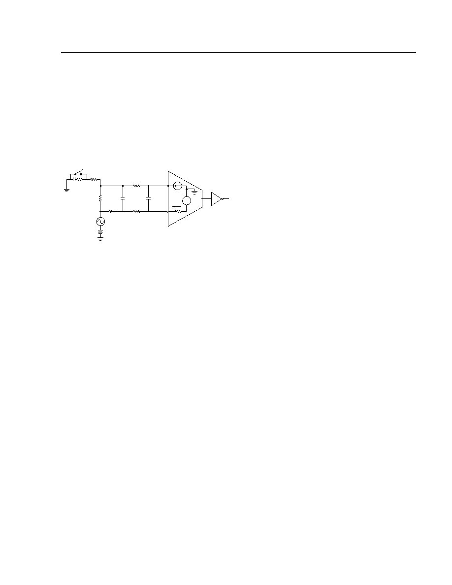
ac equivalent circuits using a T7513 Codec are shown in Figures 32 and 33.
12-2554.a (C)
Figure 32. ac Equivalent Circuit Not Including Spare Op Amp
12-3013 (C)
Figure 33. ac Equivalent Circuit Including Spare Op Amp
+
≠
+
≠
+
≠
R
P
PR 40
Z
T
+
≠
R
P
PT 40
V
T/R
I
T/R
A
V
= ≠1
A
V
= 1
≠0.4 V/mA
R
T1
R
RCV
R
HB1
R
T2
VITR
RCVN
RCVP
R
X
VGSX
VFXIN
VFXIP
VFR
(PWROP)
T7513 CODEC
ATT7564 SLIC
V
S
Z
T/R
A
V
= 4
R
G
L7554 SLIC
+
≠
R
GN
+
≠
R
T3
R
RCV
R
HB1
R
X
VGSX
VFXIN
VFXIP
VFR
(PWROP)
T7513 CODEC
+
≠
R
P
PR 40
Z
T
+
≠
R
P
PT 40
V
T/R
I
T/R
A
V
= ≠1
A
V
= 1
≠0.4 V/mA
VITR
RCVN
RCVP
V
S
Z
T/R
A
V
= 4
+
≠
Z
T5
R
T6
XMT
SN
R
T4
AGND
L7554 SLIC

26
26
Lucent Technologies Inc.
Data Sheet
March 1997
L7554 Low-Power SLIC
R
H B
R
X
gtx
g
rcv
◊
--------------------
=
Applications
(continued)
ac Design
(continued)
Example 1, Real Termination
The following design equations refer to the circuit in
Figure 32. Use these to synthesize real termination
impedance.
Termination Impedance:
Receive Gain:
Transmit Gain:
Hybrid Balance:
hbal = 20log
To optimize the hybrid balance, the sum of the currents
at the VFX input of the codec op amp should be set to
0. The following expressions assume that the test net-
work is the same as the termination impedance.
Example 2, Complex Termination:
For complex termination, the spare op amp is used
(see Figure 33).
The hybrid balance equation is the same as in
Example 1.
PCB Layout Information
Make the leads to BGND and V
BAT
as wide as possible
for thermal and electrical reasons. Also, maximize the
amount of PCB copper in the area of--and specifically
on--the leads connected to this device for the lowest
operating temperature.
When powering the device, ensure that no external
potential creates a voltage on any pin of the device that
exceeds the device ratings. In this application, some of
the conditions that cause such potentials during pow-
erup are the following: 1) an inductor connected to PT
and PR (this can force an overvoltage on V
BAT
through
the protection devices if the V
BAT
connection chatters)
and 2) inductance in the V
BAT
lead (this could resonate
with the V
BAT
filter capacitor to cause a destructive
overvoltage).
This device is normally used on a circuit card that is
subjected to hot plug-in, meaning the card is plugged
into a biased backplane connector. In order to prevent
damage to the IC, all ground connections must be
applied before, and removed after, all other connec-
tions.
z
t
v
T R
/
i
t r
≠
----------
=
z
t
2R
P
80
3200
1
R
T 1
R
G P
---------
R
T 1
R
R C V
------------
+
+
-----------------------------------
+
+
=
g
rcv
v
T R
/
v
f r
----------
=
g
rcv
8
1
R
R CV
R
T 1
-----------
R
R C V
R
G P
------------
+
+
1
z
t
Z
T R
/
----------
+
-------------------------------------------------------------------
=
g
tx
v
g s x
v
T R
/
----------
=
g
t x
R
X
R
T 2
--------
400
Z
T R
/
----------
◊
=
V
gsx
Vfr
------------
h
b a l
20
R
X
R
H B
---------
gtx
g
r c v
◊
≠
log
=
z
t
2R
P
80
3200
1
R
T 3
R
G N
---------
R
T 3
R
R C V
------------
+
+
-----------------------------------
Z
T5
R
T4
---------
(
)
+
+
=
2R
P
80
k Z
T5
(
)
+
+
=
grcv
8
1
R
RCV
R
T3
--------------
R
RCV
R
GN
--------------
+
+
1
z
t
Z
T/R
----------
+
----------------------------------------------------------------------------
=
gtx
R
≠
X
R
T
6
-----------
400
Z
T/R
----------
◊
Z
T5
R
T4
---------
◊
=
Lucent Technologies Inc.
27
Data Sheet
March 1997
L7554 Low-Power SLIC
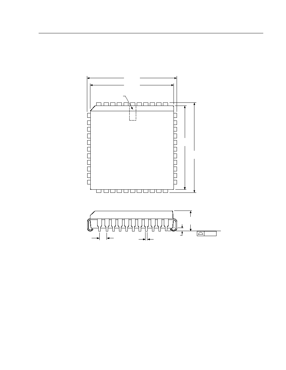
Outline Diagram
44-Pin PLCC
Controlling dimensions are in millimeters.
5-2506r7 (C)
4.57
MAX
1.27 TYP
0.53
MAX
0.10
SEATING PLANE
0.51 MIN
TYP
1
6
40
7
17
29
39
18
28
PIN #1 IDENTIFIER
ZONE
16.66 MAX
17.65 MAX
16.66
MAX
17.65
MAX

Data Sheet
March 1997
L7554 Low-Power SLIC
For additional information, contact your Microelectronics Group Account Manager or the following:
INTERNET: http://www.lucent.com/micro
U.S.A.: Microelectronics Group, Lucent Technologies Inc., 555 Union Boulevard, Room 30L-15P-BA, Allentown, PA 18103
1-800-372-2447, FAX 610-712-4106 (In CANADA: 1-800-553-2448, FAX 610-712-4106), e-mail docmaster@micro.lucent.com
ASIA PACIFIC:
Microelectronics Group, Lucent Technologies Singapore Pte. Ltd., 77 Science Park Drive, #03-18 Cintech III, Singapore 118256
Tel. (65) 778 8833, FAX (65) 777 7495
JAPAN: Microelectronics Group, Lucent Technologies Japan Ltd., 7-18, Higashi-Gotanda 2-chome, Shinagawa-ku, Tokyo 141, Japan
Tel. (81) 3 5421 1600, FAX (81) 3 5421 1700
For data requests in Europe:
MICROELECTRONICS GROUP DATALINE: Tel. (44) 1734 324 299, FAX (44) 1734 328 148
For technical inquiries in Europe:
CENTRAL EUROPE: (49) 89 95086 0 (Munich), NORTHERN EUROPE: (44) 1344 865 900 (Bracknell UK),
FRANCE: (33) 1 41 45 77 00 (Paris), SOUTHERN EUROPE: (39) 2 6601 1800 (Milan) or (34) 1 807 1700 (Madrid)
Lucent Technologies Inc. reserves the right to make changes to the product(s) or information contained herein without notice. No liability is assumed as a result of their use or application. No
rights under any patent accompany the sale of any such product(s) or information.
Copyright © 1997 Lucent Technologies Inc.
All Rights Reserved
Printed in U.S.A.
March 1997
DS97-202ALC (Replaces DS96-229LCAS)
Printed On
Recycled Paper
Ordering Information
*Devices on tape and reel must be ordered in 1000-piece increments.
Device Part No.
Description
Package
Comcode
ATTL7554AP
Low-Power SLIC, ≠60 V
44-Pin PLCC
107080921
ATTL7554AP≠TR*
Low-Power SLIC, ≠60 V
44-Pin PLCC (Tape and Reel)
107177172
ATTL7554BP
Low-Power SLIC, ≠72 V
44-Pin PLCC
107548927
ATTL7554BP≠TR*
Low-Power SLIC, ≠72 V
44-Pin PLCC (Tape and Reel)
107548943