
Data Sheet
January 2000
L7556, L7557 Low-Power SLICs
with Battery Switch
Features
s
Auxiliary input for second battery, and internal
switch to enable its use to save power
s
Low active power (typical 125 mW during on-hook
transmission)
s
Supports meter pulse injection
s
Spare op amp for meter pulse filtering
s
≠16 V to ≠60 V power supply operation
s
Distortion-free on-hook transmission
s
Convenient operating states:
-- Forward powerup
-- Disconnect (high impedance)
-- 2-wire wink (zero loop voltage)
s
Adjustable supervision functions:
-- Off-hook detector with longitudinal rejection
-- Ground key detector
-- Ring trip detector
s
Independent, adjustable, dc and ac parameters:
-- dc feed resistance
-- Loop current limit
-- Termination impedance
s
Thermal protection
Description
These electronic subscriber loop interface circuits
(SLICs) are optimized for low power consumption
while providing an extensive set of features.
The SLICs include an auxiliary battery input and a
built-in switch. In short-loop applications, they can be
used in high battery to present a high on-hook volt-
age, and then switched to low battery to reduce off-
hook power.
The SLICs also include a summing node for meter
pulse injection to 2.2 Vrms. A spare, uncommitted op
amp is included for meter pulse filtering.
The switched battery is applied to the power amplifi-
ers of the device. There are two versions. The L7556
has the battery switch completely under processor
control. The L7557 can automatically switch to lower
battery when appropriate and includes hysteresis to
avoid frequent switching. To make the switch silent,
an external capacitor can be added to slow the tran-
sition.
The L7556 is suited for applications serving only
short loops, where a high on-hook voltage is required
for compatibility with preexisting standards.
The L7557 is suited for applications where a full loop
range is needed, but low short-loop power is desired.
It is a much lower-cost solution than a switching reg-
ulator, and also occupies much less PCB area, need-
ing only a battery filter capacitor and a diode for
implementation.
The device is available in a 32-pin PLCC package. It
is built by using a 90 V complementary bipolar inte-
grated circuit (CBIC) process.

2
Lucent Technologies Inc.
Data Sheet
January 2000
with Battery Switch
L7556, L7557 Low-Power SLICs
Table of Contents
Contents Page
Features ..................................................................... 1
Description .................................................................. 1
Pin Information ............................................................ 4
Functional Description ................................................. 6
Absolute Maximum Ratings ........................................ 6
Recommended Operating Conditions ......................... 7
Electrical Characteristics ............................................. 7
Ring Trip Requirements ......................................... 11
Test Configurations .................................................. 12
Applications .............................................................. 14
Design Considerations ........................................... 16
Characteristic Curves............................................. 17
dc Applications ....................................................... 20
Battery Feed......................................................... 20
Switching the Battery............................................ 20
Overhead Voltage ............................................... 21
Adjusting Overhead Voltage ................................ 21
Adjusting dc Feed Resistance.............................. 22
Loop Range.......................................................... 22
Off-Hook Detection .............................................. 22
Ring Trip Detection.............................................. 23
Ring Ground Detection........................................ 23
ac Design ............................................................... 24
First-Generation Codecs ..................................... 24
Second-Generation Codecs ................................ 24
Third-Generation Codecs .................................... 24
Selection Criteria ................................................. 24
PCB Layout Information ............................................ 26
Outline Diagram......................................................... 27
32-Pin PLCC ........................................................... 27
Ordering Information.................................................. 28
Tables Page
Table 1. Pin Descriptions ............................................ 4
Table 2. Input State Coding ........................................ 6
Table 3. Supervision Coding ....................................... 6
Table 4. Power Supply ................................................ 7
Table 5. 2-Wire Port .................................................... 8
Table 6. Analog Pin Characteristics ............................ 9
Table 7. Uncommitted Op Amp Characteristics .......... 9
Table 8. ac Feed Characteristics .............................. 10
Table 9. Logic Inputs and Outputs ............................ 11
Table 10. Parts List for Loop Start and Ground
Start Applications ...................................... 15
Table 11. 600
Design Parameters ......................... 16
Figures Page
Figure 1. Functional Diagram ..................................... 3
Figure 2. Pin Diagram (PLCC Chip) ........................... 4
Figure 3. Ring Trip Circuits ....................................... 11
Figure 4. Basic Test Circuit ....................................... 12
Figure 5. Longitudinal Balance ................................. 12
Figure 6. Longitudinal PSRR .................................... 13
Figure 7. RFI Rejection ............................................. 13
Figure 8. Longitudinal Impedance ............................ 13
Figure 9. Metallic PSRR ........................................... 13
Figure 10. ac Gains ..................................................13
Figure 11. Basic Loop Start Application Circuit
Using T7504 Type Codec ........................14
Figure 12. Ring Ground Detection Circuit ................. 14
Figure 13. Receive Gain and Hybrid Balance vs.
Frequency ............................................... 17
Figure 14. Transmit Gain and Return Loss vs.
Frequency ............................................... 17
Figure 15. Typical V
CC
Power Supply Rejection ....... 17
Figure 16. Typical V
BAT
Power Supply
Rejection ................................................. 17
Figure 17. Loop Closure Program Resistor
Selection ..................................................18
Figure 18. Ring Ground Detection Programming .....18
Figure 19. Loop Current vs. Loop Voltage ................ 18
Figure 20. Loop Current vs. Loop Resistance .......... 18
Figure 21. Typical SLIC Power Dissipation vs.
Loop Resistance ...................................... 19
Figure 22. Power Derating ........................................ 19
Figure 23. Longitudinal Balance Resistor Mismatch
Requirements .......................................... 19
Figure 24. Longitudinal Balance vs. Protection
Resistor Mismatch ................................... 19
Figure 25. Loop Current vs. Loop Voltage ................ 20
Figure 26. SLIC 2-Wire Output Stage ....................... 21
Figure 27. Equivalent Circuit for Adjusting the Over-
head Voltage ........................................... 21
Figure 28. Equivalent Circuit for Adjusting the dc
Feed Resistance ...................................... 22
Figure 29. Adjusting Both Overhead Voltage and dc
Feed Resistance .....................................22
Figure 30. Off-Hook Detection Circuit
Applications ............................................. 22
Figure 31. Ring Trip Equivalent Circuit and
Equivalent Application ............................. 23
Figure 32. ac Equivalent Circuit Not Including Spare
Op Amp ................................................... 25
Figure 33. ac Equivalent Circuit Including Spare
Op Amp ................................................... 25
Lucent Technologies Inc.
3
Data Sheet
January 2000
with Battery Switch
L7556, L7557 Low-Power SLICs
Description
(continued)
12-2551.a (F)
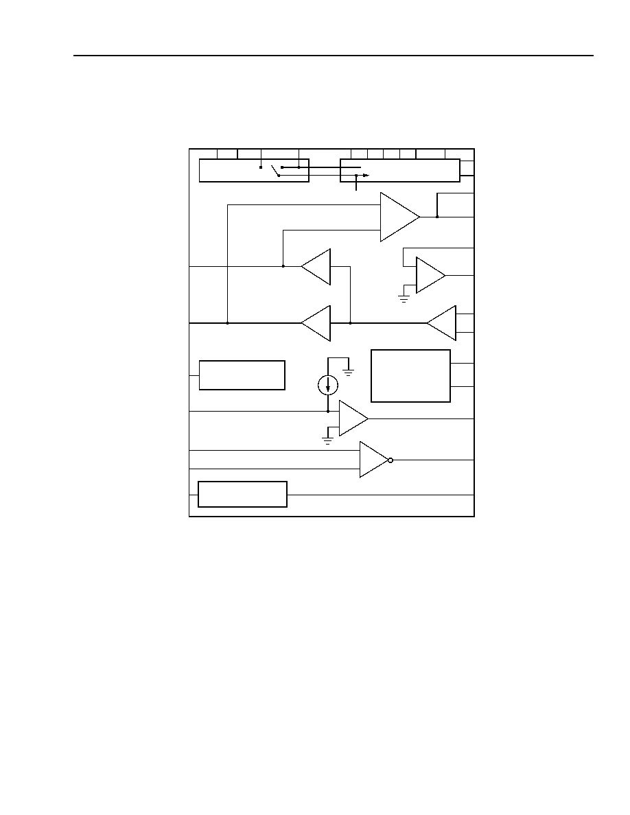
Figure 1. Functional Diagram
+
≠
+
≠
≠
+
≠
+
+
≠
A = 4
A = ≠4
BATTERY
AG
ND
V
BAT
2
V
CC
CF1
PT
PR
dc RESISTANCE
ADJUST
DCR
ICM
RTSN
RTSP
LCTH
RING GROUND
DETECTOR
RING TRIP DETECTOR
LOOP CLOSURE DETECTOR
BATTERY FEED
STATE CONTROL
SPARE
OP AMP
DCOUT
VITR
B0
RCVP
RCVN
XMT
B1
SN
NLC
RGDET
NRDET
CF2
1 V/8 mA
SWITCH
BG
ND
I
PR
O
G
BS2
BS1
BS
V
BAT
1
L
BA
T
V
REG
POWER CONDITIONING
& REFERENCE
4
Lucent Technologies Inc.
Data Sheet
January 2000
with Battery Switch
L7556, L7557 Low-Power SLICs
Pin Information
12-2548.q (F)
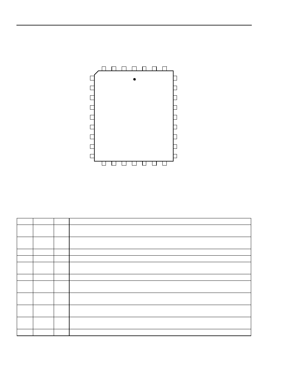
Figure 2. Pin Diagram (PLCC Chip)
Table 1. Pin Descriptions
Pin
Symbol Type
Description
1
V
BAT2
--
Auxiliary Battery Supply. Negative high-voltage battery, lower in magnitude than
V
BAT1
, used to reduce power dissipation on short loops.
2
I
PROG
I
Current-Limit Program Input. A resistor to DCOUT sets the dc current limit of the
device.
3
BS
I
Battery Switch. See Table 2 for description.
4
NC
--
No Connection (L7556 Only). Do not use as a tie point.
4
L
BAT
O
Lower Battery in Use (L7557 Only). When high, this open-collector output indicates
the device has switched to V
BAT2.
To use, connect a 100 k
resistor to V
CC
.
5
V
CC
--
+5 V Power Supply.
6
RCVP
I
Receive ac Signal Input (Noninverting). This high-impedance input controls the ac
differential voltage on tip and ring.
7
RCVN
I
Receive ac Signal Input (Inverting). This high-impedance input controls the ac differ-
ential voltage on tip and ring.
8
LCTH
I
Loop Closure Threshold Input. Connect a resistor to DCOUT to set off-hook thresh-
old.
9
DCOUT
O
dc Output Voltage. This output is a voltage that is directly proportional to the absolute
value of the differential tip/ring current.
10
V
BAT1
--
Battery Supply. Negative high-voltage power supply, higher in magnitude than V
BAT2
.
B1
XMT
NLC
NRDET
RTSP
RTSN
PT
5
7
8
9
10
11
12
13
14
15
6
4
3
2
1
32
31
16
18
19
20
17
30
27
26
25
24
23
22
21
28
ICM
DCR
AG
ND
AG
ND
VI
TR
RGDET
B0
29
SN
BGND
I
PRO
G
RCVN
RCVP
V
CC
LCTH
V
BAT1
DCOUT
PR
CF2
CF1
NC
32-PIN PLCC
BS2
BS1
V
BA
T2
BS
NC
L
BAT

Lucent Technologies Inc.
5
Data Sheet
January 2000
with Battery Switch
L7556, L7557 Low-Power SLICs
Pin Information
(continued)
Table 1. Pin Descriptions
(continued)
Pin
Symbol Type
Description
11
PR
I/O
Protected Ring. The output of the ring driver amplifier and input to loop sensing cir-
cuitry. Connect to loop through overvoltage protection.
12
CF2
--
Filter Capacitor 2. Connect a 0.1 µF capacitor from this pin to AGND.
13
CF1
--
Filter Capacitor 1. Connect a 0.47 µF capacitor from this pin to pin CF2.
14
VITR
O
Transmit ac Output Voltage. This output is a voltage that is directly proportional to the
differential tip/ring current.
15
ICM
I
Common-Mode Current Sense. To program ring ground sense threshold, connect a
resistor to V
CC
and connect a capacitor to AGND to filter 50/60 Hz. If unused, the pin
can be left unconnected.
16
RGDET
O
Ring Ground Detect. When high, this open-collector output indicates the presence of
a ring ground. To use, connect a 100 k
resistor to V
CC
.
17
B0
I
State Control Input. B0 and B1 determine the state of the SLIC. See Table 2.
18
AGND
--
Analog Signal Ground.
19
AGND
--
Analog Signal Ground.
20
DCR
I
dc Resistance for Low Loop Currents. Leave open for dc feed resistance of 115
,
or short to DCOUT for 615
. Intermediate values can be set by a simple resistor
divider from DCOUT to ground with the tap at DCR.
21
BGND
--
Battery Ground. Ground return for the battery supply.
22
PT
I/O
Protected Tip. The output of the tip driver amplifier and input to loop sensing circuitry.
Connect to loop through overvoltage protection.
23
RTSN
I
Ring Trip Sense Negative. Connect this pin to the ringing generator signal through a
high-value resistor.
24
RTSP
I
Ring Trip Sense Positive. Connect this pin to the ring relay and the ringer series resis-
tor through a high-value resistor.
25
NRDET
O
Ring Trip Detector Output. When low, this logic output indicates that ringing is tripped.
26
NLC
O
Loop Detector Output. When low, this logic output indicates an off-hook condition.
27
B1
I/O
State Control Input. B0 and B1 determine the state of the SLIC. See Table 2. Pin B1
has a 40 k
pull-up. It goes low in the event of thermal shutdown.
28
XMT
O
Transmit ac Output Voltage. The output of the uncommitted operational amplifier.
29
SN
I
Summing Node. The inverting input of the uncommitted operational amplifier. A resis-
tor or network to XMT sets the gain.
30
NC
--
No Connection. Do not use as a tie point.
31
BS2
--
Battery Switch Slowdown. A 0.1 µF capacitor from BS1 to BS2 will ramp the battery
switch transition for applications requiring quiet transition. If not needed, the pin can be
left open.
32
BS1
--
Battery Switch Slowdown. A 0.1 µF capacitor from BS1 to BS2 will ramp the battery
switch transition for applications requiring quiet transition. If not needed, the pin can be
left open.