Data Sheet
November 1999
L7582 Tip Ring Access Switch
Features
s
Small size/surface-mount packaging
s
Monolithic IC reliability
s
Low impulse noise
s
Make-before-break, break-before-make operation
s
Clean, bounce-free switching
s
Low, matched ON-resistance
s
Built-in current limiting, thermal shutdown, and
SLIC protection
s
5 V only operation, very low power consumption
s
Battery monitor, all OFF state upon loss of battery
s
No EMI
s
Latched logic level inputs, no drive circuitry
s
Only one external protector required
Applications
s
Central office
s
DLC
s
PBX
s
DAML
s
HFC/FITL
Description
The L7582 Tip Ring Access Switch is a monolithic
solid-state device that provides the switching
functionality of a 2 form C switch.
The L7582 is designed to provide power ringing
access to tip and ring in central office, digital loop
carrier, private branch exchange, digitally added
main line, and hybrid fiber coax/fiber-in-the-loop ana-
log line card applications. An additional pair of solid-
state contacts provides access to the telephone loop
for line test access or message waiting in the PBX
application.
The L7582 has four states: the idle talk state (line
break switches closed, ringing and loop access
switches open), the power ringing state (ringing
access switches closed, line break and loop access
switches open), loop access state (loop access
switches closed, line break and ringing access
switches open), and an all OFF state.
The L7582 offers break-before-make or make-before-
break switching, with simple logic level input control.
Because of the solid-state construction, voltage tran-
sients generated when switching into an inductive
ringing load during ring cadence or ring trip are mini-
mized, possibly eliminating the need for external zero
cross switching circuitry. State control is via logic
level inputs so no additional driver circuitry is
required.
The line break switch is a linear switch that has
exceptionally low ON-resistance and an excellent
ON-resistance matching characteristic. The ringing
access switch has a breakdown voltage rating
>480 V which is sufficiently high, with proper protec-
tion, to prevent breakdown in the presence of a tran-
sient fault condition (i.e., passing the transient on to
the ringing generator).
Incorporated into the L7582Axx is a diode bridge/
SCR clamping circuit, current-limiting circuitry, and a
thermal shutdown mechanism to provide protection
to the SLIC device and subsequent circuitry during
fault conditions (see Figure 1). Positive and negative
lightning is reduced by the current-limiting circuitry
and steered to ground via diodes and the integrated
SCR. Power cross is also reduced by the current-
limiting and thermal shutdown circuits.

2
2
Lucent Technologies Inc.
Data Sheet
November 1999
L7582 Tip Ring Access Switch
Description
(continued)
The L7582Bxx version provides only an integrated
diode bridge along with current limiting and thermal
shutdown as shown in Figure 2. This will cause positive
faults to be directed to ground and negative faults to
battery. In either polarity, faults are reduced by the cur-
rent-limit and/or thermal shutdown mechanisms.
To protect the L7582 from an overvoltage fault condi-
tion, use of a secondary protector is required. The sec-
ondary protector must limit the voltage seen at the tip/
ring terminals to prevent the breakdown voltage of the
switches from being exceeded. To minimize stress on
the solid-state contacts, use of a foldback- or crowbar-
type secondary protector is recommended. With proper
choice of secondary protection, a line card using the
L7582 will meet all relevant ITU-T, LSSGR, FCC, or
UL*
protection requirements.
The L7582 operates from a 5 V supply only. This
gives the device extremely low idle and active power
dissipation and allows use with virtually any range of
battery voltage. This makes the L7582 especially
appropriate for remote power applications such as
DAML or FOC/FITL or other Bellcore TA 909 applica-
tions where power dissipation is particularly critical.
A battery voltage is also used by the L7582, only as a
reference for the integrated protection circuit. The
L7582 will enter an all OFF state upon loss of battery.
During power ringing, to turn on and maintain the ON
state, the ring access switch will draw a nominal 2 mA
or 4 mA from the ring generator.
The L7582 device is packaged in a 16-pin, plastic DIP
package (L7582AC/BC) and a 16-pin, plastic SOG
package (L7582AAE/BAE). The L7582AAE/BAE are
pin compatible with the L7542AAE/BAE.
*
UL
is a registered trademark of Underwriters Laboratories, Inc.
Pin Information
12-2306.i (F)
Note: Shown with A version protection. The 16-pin SOG is available
with either A or B version protection.
Figure 1. 16-Pin, Plastic SOG
12-2306.c (F)
Note: Shown with B version protection. The 16-pin DIP is available
with either A or B version protection.
Figure 2. 16-Pin, Plastic DIP
1
2
3
4
5
6
7
8
16
15
14
13
12
11
10
9
V
BAT
R
BAT
R
LINE
LATCH
IN
RING
IN
ACCESS
R
ACCESS
F
GND
T
ACCESS
V
DD
D
GND
CONTROL
LOGIC
SW1
SW2
SW5
SW3
SCR
T
BAT
T
LINE
T
RINGING
T
SD
R
RINGING
SW4
SW6
AND
TRIP
CKT
1
2
3
4
5
6
7
8
16
15
14
13
12
11
10
9
V
BAT
R
BAT
R
LINE
LATCH
IN
RING
IN
ACCESS
R
ACCESS
F
GND
T
ACCESS
V
DD
D
GND
CONTROL
LOGIC
SW1
SW2
SW5
SW3
T
BAT
T
LINE
T
RINGING
T
SD
R
RINGING
SW4
SW6
Lucent Technologies Inc.
3
Data Sheet
November 1999
L7582 Tip Ring Access Switch
Pin Information
(continued)
Table 1. Pin Descriptions
DIP SOG Symbol
Description
DIP
SOG
Symbol
Description
1
1
F
GND
Fault ground.
16
16
V
BAT
Battery voltage. Used as a ref-
erence for protection circuit.
2
2
T
BAT
Connect to TIP on SLIC side.
15
15
R
BAT
Connect to RING on SLIC side.
3
3
T
LINE
Connect to TIP on line side.
14
14
R
LINE
Connect to RING on line side.
4
4
T
RINGING
Connect to return ground for ring-
ing generator.
13
13
R
RINGING
Connect to ringing generator.
5
5
T
ACCESS
Test access.
12
12
R
ACCESS
Test access.
6
6
V
DD
5 V supply.
11
11
LATCH
Data latch control, active-high,
transparent low.
7
7
T
SD
Temperature shutdown pin. Can
be used as a logic level input or
output. See Table 13, Truth Table,
and the Switching Behavior sec-
tion of this data sheet for input pin
description. As an output, will
read 5 V when device is in its
operational mode and 0 V in the
thermal shutdown mode. To dis-
able the thermal shutdown mech-
anism, tie this pin to 5 V (not
recommended).
10
10
IN
RING
Logic level input switch control.
8
8
D
GND
Digital ground.
9
9
IN
ACCESS
Logic level input switch control.
Absolute Maximum Ratings
Stresses in excess of the absolute maximum ratings
can cause permanent damage to the device. These are
absolute stress ratings only. Functional operation of the
device is not implied at these or any other conditions in
excess of those given in the operational sections of the
data sheet. Exposure to absolute maximum ratings for
extended periods can adversely affect device reliability.
Table 2. Absolute Maximum Ratings Parameters
Handling Precautions
Although protection circuitry has been designed into
this device, proper precautions should be taken to
avoid exposure to electrostatic discharge (ESD) during
handling and mounting. Lucent Technologies Micro-
electronics Group employs a human-body model
(HBM) and a charged-device model (CDM) for ESD-
susceptibility testing and protection design evaluation.
ESD voltage thresholds are dependent on the circuit
parameters used to define the model. No industry-wide
standard has been adopted for CDM. However, a stan-
dard HBM (resistance = 1500
, capacitance = 100 pF)
is widely used and therefore can be used for compari-
son purposes. The HBM ESD threshold presented
here was obtained by using these circuit parameters.
Table 3. HBM ESD Threshold Voltage
Parameter
Min
Max
Unit
Operating Temperature Range
≠40
110
∞
C
Storage Temperature Range
≠40
150
∞
C
Relative Humidity Range
5
95
%
Pin Soldering Temperature (t =
10 s max)
--
260
∞
C
5 V Power Supply
--
7
V
Battery Supply
--
≠85
V
Logic Input Voltage
--
7
V
Input-to-output Isolation
--
330
V
Pole-to-pole Isolation
--
330
V
Device
Rating
L7582
1000 V
4
4
Lucent Technologies Inc.
Data Sheet
November 1999
L7582 Tip Ring Access Switch
Electrical Characteristics
T
A
= ≠40
∞
C to +85
∞
C, unless otherwise specified.
Minimum and maximum values are testing requirements. Typical values are characteristics of the device and are
the result of engineering evaluations. Typical values are for information purposes only and are not part of the test-
ing requirements.
Table 4. Power Supply Specifications
* V
BAT
is used only as a reference for internal protection circuitry. If V
BAT
rises above ≠10 V, the device will enter an all OFF state and will remain
in the all OFF state until the battery voltage drops below ≠15 V.
Table 5. Break Switches, 1 and 2
* This parameter is not tested in production. Choice of secondary protector should ensure this rating is not exceeded.
Applied voltage is 100 Vp-p square wave at 100 Hz.
Supply
Min
Typ
Max
Unit
V
DD
4.5
5
5.5
V
V
BAT*
≠19 --
≠72
V
Parameter
Test Condition
Measure
Min
Typ
Max
Unit
OFF-state Leakage
Current:
+25
∞
C
+85
∞
C
≠40
∞
C
Vswitch (differential) = ≠320 V to Gnd
Vswitch (differential) = ≠60 V to +260 V
Vswitch (differential) = ≠330 V to Gnd
Vswitch (differential) = ≠60 V to +270 V
Vswitch (differential) = ≠310 V to Gnd
Vswitch (differential) = ≠60 V to +250 V
Iswitch
Iswitch
Iswitch
--
--
--
--
--
--
1
1
1
µ
A
µ
A
µ
A
ON-resistance
(SW1, SW2):
+25
∞
C
+85
∞
C
≠40
∞
C
T
LINE
=
±
10 mA,
±
40 mA, T
BAT
= ≠2 V
T
LINE
=
±
10 mA,
±
40 mA, T
BAT
= ≠2 V
T
LINE
=
±
10 mA,
±
40 mA, T
BAT
= ≠2 V
V
ON
V
ON
V
ON
--
--
--
19.5
--
14.5
--
28
--
ON-resistance Match
Per ON-resistance test
condition of SW1, SW2
Magnitude
R
ON
SW1 ≠ R
ON
SW2
--
0.2
1.0
ON-state Voltage*
Iswitch = I
LIMIT
@ 50 Hz/60 Hz
V
ON
--
--
220
V
dc Current Limit:
+85
∞
C
≠40
∞
C
Vswitch (on) =
±
10 V
Vswitch (on) =
±
10 V
Iswitch
Iswitch
80
--
--
--
--
250
mA
mA
Dynamic Current Limit
(t = < 0.5
µ
s)
Break switches in ON state; ringing
access switches off; apply
±
1000 V at
10/1000
µ
s pulse; appropriate second-
ary protection in place
Iswitch
--
2.5
--
A
Isolation:
+25
∞
C
+85
∞
C
≠40
∞
C
Vswitch (both poles) =
±
320 V,
Logic inputs = Gnd
Vswitch (both poles) =
±
330 V,
Logic inputs = Gnd
Vswitch (both poles) =
±
310 V,
Logic inputs = Gnd
Iswitch
Iswitch
Iswitch
--
--
--
--
--
--
1
1
1
µ
A
µ
A
µ
A
dV/dt Sensitivity
--
--
--
200
--
V/µs

Lucent Technologies Inc.
5
Data Sheet
November 1999
L7582 Tip Ring Access Switch
Electrical Characteristics
(continued)
Table 6. Ring Return Switch, 3
* This parameter is not tested in production. Choice of secondary protector should ensure this rating is not exceeded.
Applied voltage is 100 Vp-p square wave at 100 Hz.
Table 7. Ringing Access Switch, 4
* At the time of publication of this data sheet, the current device design will be a nominal 4 mA. Devices are being redesigned to reduce this
current to less than 2 mA nominally. Consult your Lucent Technologies Microelectronics Group account executive for additional details.
Choice of secondary protector and series current-limit resistor should ensure these ratings are not exceeded.
Applied voltage is 100 Vp-p square wave at 100 Hz.
Parameter
Test Condition
Measure Min
Typ Max Unit
OFF-state Leakage
Current (SW3):
+25
∞
C
+85
∞
C
≠40
∞
C
Vswitch (differential) = ≠320 V to Gnd
Vswitch (differential) = ≠60 V to +260 V
Vswitch (differential) = ≠330 V to Gnd
Vswitch (differential) = ≠60 V to +270 V
Vswitch (differential) = ≠310 V to Gnd
Vswitch (differential) = ≠60 V to +250 V
Iswitch
Iswitch
Iswitch
--
--
--
--
--
--
1
1
1
µ
A
µ
A
µ
A
dc Current Limit
Vswitch (on) =
±
10 V
Iswitch
--
200
--
mA
Dynamic Current
Limit (t = < 0.5
µ
s)
Break switches in ON state; ringing access switches
off; apply
±
1000 V at 10/1000
µ
s pulse; appropriate
secondary protection in place
Iswitch
--
2.5
--
A
ON-resistance
Iswitch (on) =
±
0 mA,
±
10 mA
V
ON
--
--
100
ON-state Voltage*
Iswitch = I
LIMIT
@ 50 Hz/60 Hz
V
ON
--
--
130
V
Isolation:
+25
∞
C
+85
∞
C
≠40
∞
C
Vswitch (both poles) =
±
320 V, Logic inputs = Gnd
Vswitch (both poles) =
±
330 V, Logic inputs = Gnd
Vswitch (both poles) =
±
310 V, Logic inputs = Gnd
Iswitch
Iswitch
Iswitch
--
--
--
--
--
--
1
1
1
µ
A
µ
A
µ
A
dV/dt Sensitivity
--
--
--
200
--
V/µs
Parameter
Test Condition
Measure
Min
Typ Max Unit
OFF-state Leakage
Current (SW4):
+25
∞
C
+85
∞
C
≠40
∞
C
Vswitch (differential) = ≠255 V to +210 V
Vswitch (differential) = +255 V to ≠210 V
Vswitch (differential) = ≠270 V to +210 V
Vswitch (differential) = +270 V to ≠210 V
Vswitch (differential) = ≠245 V to +210 V
Vswitch (differential) = +245 V to ≠210 V
Iswitch
Iswitch
Iswitch
--
--
--
--
--
--
1
1
1
µ
A
µ
A
µ
A
ON Voltage
Iswitch (on) =
±
1 mA
--
--
--
3
V
Ring Generator Cur-
rent During Ring
V
CC
= 5 V
IN
ACCESS
= 0
I
RINGSOURCE
--
*
--
mA
Steady-state Current
--
--
--
--
150
mA
Surge Current
--
--
--
--
2
A
Release Current
--
--
--
500
--
µ
A
ON-resistance
Iswitch (on) =
±
70 mA,
±
80 mA
V
on
--
12
Isolation:
+25
∞
C
+85
∞
C
≠40
∞
C
Vswitch (both poles) =
±
320 V, Logic inputs = Gnd
Vswitch (both poles) =
±
330 V, Logic inputs = Gnd
Vswitch (both poles) =
±
310 V, Logic inputs = Gnd
Iswitch
Iswitch
Iswitch
--
--
--
--
--
--
1
1
1
µ
A
µ
A
µ
A
dV/dt Sensitivity
--
--
--
200
--
V/
µ
s

6
Lucent Technologies Inc.
Data Sheet
November 1999
L7582 Tip Ring Access Switch
Electrical Characteristics
(continued)
Table 8. Loop Access Switches, 5 and 6
* This parameter is not tested in production. Choice of secondary protector should ensure this rating is not exceeded.
Applied voltage is 100 Vp-p square wave at 100 Hz.
Parameter
Test Condition
Measure
Min
Typ Max Unit
OFF-state Leakage
Current:
+25
∞
C
+85
∞
C
≠40
∞
C
Vswitch (differential) = ≠320 V to Gnd
Vswitch (differential) = ≠60 V to +260 V
Vswitch (differential) = ≠330 V to Gnd
Vswitch (differential) = ≠60 V to +270 V
Vswitch (differential) = ≠310 V to Gnd
Vswitch (differential) = ≠60 V to +250 V
Iswitch
Iswitch
Iswitch
--
--
--
--
--
--
1
1
1
µ
A
µ
A
µ
A
dc Current Limit:
+85
∞
C
≠40
∞
C
Vswitch (on) =
±
10 V
Vswitch (on) =
±
10 V
Iswitch
Iswitch
80
--
--
--
--
250
mA
mA
Dynamic Current Limit
(t = <0.5
µ
s)
Break switches in ON state; ringing access
switches off; apply
±
1000 V at 10/1000
µ
s pulse;
appropriate secondary protection in place
Iswitch
--
2.5
--
A
ON-resistance:
+25
∞
C
+85
∞
C
≠40
∞
C
Iswitch (on) =
±
10 mA,
±
40 mA
Iswitch (on) =
±
10 mA,
±
40 mA
Iswitch (on) =
±
10 mA,
±
40 mA
V
ON
V
ON
V
ON
--
--
--
45
--
33
--
70
--
ON-state Voltage*
Iswitch = I
LIMIT
@ 50 Hz/60 Hz
V
ON
--
--
130
V
Isolation:
+25
∞
C
+85
∞
C
≠40
∞
C
Vswitch (both poles) =
±
320 V, Logic inputs = Gnd
Vswitch (both poles) =
±
330 V, Logic inputs = Gnd
Vswitch (both poles) =
±
310 V, Logic inputs = Gnd
Iswitch
Iswitch
Iswitch
--
--
--
--
--
--
1
1
1
µ
A
µ
A
µ
A
dV/dt Sensitivity
--
--
--
200
--
V/µs

Lucent Technologies Inc.
7
Data Sheet
November 1999
L7582 Tip Ring Access Switch
Electrical Characteristics
(continued)
Table 9. Additional Electrical Characteristics
* Temperature shutdown flag (TSD) will be high during normal operation and low during temperature shutdown state.
Parameter
Test Condition
Measure
Min
Typ
Max Unit
Digital Input Characteristics:
Input Low Voltage
--
--
--
--
1.5
V
Input High Voltage
--
--
3.5
--
--
V
Input Leakage Current (high)
V
DD
= 5.5 V, V
BAT
= ≠75 V,
Vlogicin = 5 V
llogicin
--
--
1
µ
A
Input Leakage Current (low)
V
DD
= 5.5 V, V
BAT
= ≠75 V,
Vlogicin = 0 V
llogicin
--
--
1
µ
A
Power Requirements:
Power Dissipation
V
DD
= 5 V, V
BAT
= ≠48 V,
idle/talk state or all OFF state,
ringing state or access state
I
DD
, I
BAT
I
DD
--
--
3
6
5
10
mW
mW
V
DD
Current
V
DD
= 5 V,
idle/talk state or all OFF state,
ringing state or access state
I
DD
I
DD
--
--
560
0.750
900
1.9
µ
A
mA
V
BAT
Current
V
BAT
= ≠48 V,
idle/talk state or all OFF state,
ringing state or access state
I
BAT
I
BAT
--
--
4
4
10
10
µ
A
µ
A
Temperature Shutdown Requirements*:
Shutdown Activation Temperature
--
--
110
125
150
∞
C
Shutdown Circuit Hysteresis
--
--
10
--
25
∞
C
Zero Cross Current Turn Off
The ring access switch (SW4) is designed to turn off on
the next zero current crossing after application of the
appropriate logic input control. This switch requires a
current zero cross to turn off. Switch 4, once on, will
remain in the ON state (regardless of logic input) until a
current zero cross. Therefore, to ensure proper opera-
tion of switch 4, this switch should be connected, via
proper impedance, to the ringing generator or some
other ac source. Do not attempt to switch pure dc with
switch 4.
For a detailed explanation of the operation of switch 4,
please refer to the
An Introduction to L758X Series of
Line Card Access Switches
Application Note.
Switching Behavior
When switching from the power ringing state to the
idle/talk state via simple logic level input control, the
L7582 is able to provide control with respect to the tim-
ing when the ringing access contacts are released rela-
tive to the state of the line break contacts.
Make-before-break operation occurs when the line
break switch contacts are closed (or made) before the
ringing access switch contact is opened (or broken).
Break-before-make operation occurs when the ringing
access contact is opened (broken) before the line
break switch contacts are closed (made).
Using the logic level input pins INring and INaccess,
either make-before-break or break-before-make opera-
tion of the L7582 is easily achieved. The logic
sequences for either mode of operation are given in
Table 10 and Table 11. See the Truth Table (Table 13)
for an explanation of the logic states.

8
Lucent Technologies Inc.
Data Sheet
November 1999
L7582 Tip Ring Access Switch
Switching Behavior
(continued)
When using an L7582 in the make-before-break mode,
during the ring-to-idle transition, for a period of up to
one-half the ringing frequency, the ring break switch
and the pnpn-type ring access switch can both be in
the ON state. This is the maximum time after the logic
signal at IN
RING
has transitioned that the ring access
switch is waiting for the next zero current cross, so it
can close. During this interval, current that is limited to
the dc break switch current-limit value will be sourced
from the ring node of the SLIC.
This current is presented to the internal protection cir-
cuit.
The SCR may turn on if:
s
The SCR-type protector is used (A code)
s
By random probability the ring-to-idle transition
occurs during a portion of the ring cycle when the
ringing voltage exceeds the protection circuit SCR
turn-on voltage.
s
Current in excess of the SCR's turn-on current is also
available.
Once the SCR is triggered on, if the SLIC is capable of
supplying current in excess of the holding current, the
SCR may be latched on by the SLIC.
The probability of this event depends on the character-
istics of the given SLIC and of the holding current of the
L7582A device. The SCR hold current distribution is
designed to be safely away from the test limit of
80 mA. The higher the distribution, the lower the proba-
bility of the latch.
If this situation is of concern for a given board design,
either use the A series device in the break-before-make
mode (eliminates the original 25 ms current pulse) or
use a B series device (eliminates the SCR).
Table 10. Make-Before-Break Operation
ACCESS INPUT
T
SD
State
Timing
Break
Switches
1 & 2
Ring
Return
Switch
3
Ring
Access
Switch
4
Line
Access
Switches
5 & 6
0 V
5 V
Float Power Ringing
--
Open
Closed
Closed
Open
0 V
0 V
Float Make-before-
break
SW4 waiting for next zero
current crossing to turn off
maximum time--one-half of
ringing. In this transition
state, current that is limited
to the dc break switch cur-
rent-limit value will be
sourced from the ring node
of the SLIC.
Closed
Open
Closed
Open
0 V
0 V
Float
Idle/Talk
Zero cross current has
occurred.
Closed
Open
Open
Open

Lucent Technologies Inc.
9
Data Sheet
November 1999
L7582 Tip Ring Access Switch
Switching Behavior
(continued)
Table 11. Break-Before-Make Operation
Notes:
Break-before-make operation can also be achieved using T
SD
as an input. In lines two and three of Table 11, instead of using the logic input pins
to force the all OFF state, force T
SD
to ground. This will override the logic inputs and also force the all OFF state. Hold this state for 25 ms. Dur-
ing this 25 ms all OFF state, toggle the inputs from 10 (ringing state) to 00 (idle/talk state). After 25 ms, release T
SD
to return switch control to
the input pins which will set the idle talk state.
When using the L7582 in this mode, forcing T
SD
to ground will override the INPUT pins and force an all OFF state. Setting T
SD
to 5 V will allow
switch control via the logic INPUT pins. However, setting T
SD
to 5 V will also disable the thermal shutdown mechanism. This is not recom-
mended. Therefore, to allow switch control via the logic INPUT pins, allow T
SD
to float.
Thus, when using T
SD
as an input, the two recommended states are 0 (overrides logic input pins and forces all OFF state) and float (allows
switch control via logic input pins and thermal shutdown mechanism is active). This may require use of an open collector buffer.
Also note that T
SD
operation in L7582 is different than T
SD
operation of the L7581, where application of 5 V does not disable the thermal shut-
down mechanism.
ACCESS INPUT
T
SD
State
Timing
Break
Switches
1 & 2
Ring
Return
Switch 3
Ring
Access
Switch 4
Line Access
Switches
5 & 6
0 V
5 V
Float
Power
Ringing
--
Open
Closed
Closed
Open
5 V
5 V
Float
All Off
Hold this state for
25 ms.
SW4 waiting for zero cur-
rent to turn off.
Open
Open
Closed
Open
5 V
5 V
Float
All Off
Zero current has occurred
and SW4 has opened.
Open
Open
Open
Open
0 V
0 V
Float
Idle/Talk Release break switches.
Closed
Open
Open
Open
Power Supplies
Both the 5 V and battery supply are brought onto the
L7582. The L7582 requires only the 5 V supply for
switch operation; that is, state control is powered exclu-
sively off of the 5 V supply. Because of this, the L7582
offers extremely low power dissipation, both in the idle
and active states.
The battery voltage is not used for switch state control.
The battery is used as a reference voltage by the
integrated secondary protection circuit. When the volt-
age at T
BAT
or R
BAT
drops 2 V to 4 V below the battery,
the integrated SCR will trigger, thus preventing
fault-induced overvoltage situations at the T
BAT
/R
BAT
nodes.
Loss of Battery Voltage
As an additional protection feature, the L7582 monitors
the battery voltage. Upon loss of battery voltage, the
L7582 will automatically enter an all OFF state and
remain in that state until the battery voltage is restored.
The L7582 is designed such that the device will enter
the all OFF state if the battery rises above ≠10 V and
will remain off until the battery drops below ≠15 V.
Monitoring the battery for the automatic shutdown fea-
ture will draw a small current from the battery, typically
4
µ
A. This will add slightly to the overall power dissipa-
tion of the device.
Impulse Noise
Using the L7582 will minimize and possibly eliminate
the contribution to the overall system impulse noise
that is associated with ringing access switches.
Because of this characteristic of the L7582, it may not
be necessary to incorporate a zero cross switching
scheme. This ultimately depends upon the characteris-
tics of the individual system and is best evaluated at
the board level.

10
10
Lucent Technologies Inc.
Data Sheet
November 1999
L7582 Tip Ring Access Switch
Protection
Integrated SLIC Protection
Diode Bridge/SCR
In the L7582Axx version, protection to the SLIC device
or other subsequent circuitry is provided by a combina-
tion of current-limited break switches, a diode bridge/
SCR clamping circuit, and a thermal shutdown mecha-
nism. In the L7582Bxx version, protection to the SLIC
device or other subsequent circuitry is provided by a
combination of current-limited break switches, a diode
bridge, and a thermal shutdown mechanism.
In both versions, during a positive lightning event, fault
current is directed to ground via steering diodes in the
diode bridge. Voltage is clamped to a diode drop above
ground. In the A version, negative lightning causes the
SCR to conduct when the voltage goes 2 V to 4 V more
negative than the battery. Fault currents are then
directed to ground via the SCR and steering diodes in
the diode bridge.
Note that for the SCR to foldback or crowbar, the ON
voltage (see Table 11) of the SCR must be less nega-
tive than the battery reference voltage. If the battery
voltage is less negative than the SCR ON voltage, the
SCR will conduct fault currents to ground; however, it
will not crowbar.
In the B version, negative lightning is directed to battery
via steering diodes in the diode bridge.
For power cross and power induction faults, in both ver-
sions, the positive cycle of the fault is clamped a diode
drop above ground and fault currents are steered to
ground. In the A version, the negative cycle will cause
the SCR to trigger when the voltage exceeds the bat-
tery reference voltage by 2 V to 4 V. When the SCR
triggers, fault current is steered to ground. In the B ver-
sion, the negative cycle of the power cross is steered to
battery.
Current Limiting
During a lightning event, the current that is passed
through the break switches and presented to the inte-
grated protection circuit and subsequent circuitry is lim-
ited by the dynamic current-limit response of the break
switches (assuming idle/talk state). When the voltage
seen at the T
LINE
/R
LINE
nodes is properly clamped by
an external secondary protector, upon application of a
1000 V 10 x 1000 pulse (LSSGR lightning), the current
seen at the T
BAT
/R
BAT
nodes will typically be a pulse of
magnitude 2.5 A and duration less than 0.5
µ
s.
During a power cross event, the current that is passed
through the break switches and presented to the inte-
grated protection circuit and subsequent circuitry is lim-
ited by the dc current-limit response of the break
switches (assuming idle/talk state). The dc current limit
is specified over temperature between 100 mA and
250 mA.
Note that the current-limit circuitry has a negative tem-
perature coefficient. Thus, if the device is subjected to
an extended power cross, the value of current seen at
T
BAT
/R
BAT
will decrease as the device heats due to the
fault current. If sufficient heating occurs, the tempera-
ture shutdown mechanism will activate and the device
will enter an all off mode.
Temperature Shutdown Mechanism
When the device temperature reaches a minimum of
110
∞
C, the thermal shutdown mechanism will activate
and force the device into an all OFF state, regardless of
the logic input pins. Pin T
SD
, when used as an output,
will read 0 V when the device is in the thermal shut-
down mode and +V
DD
during normal operation.
During a lightning event, due to the relatively short
duration, the thermal shutdown will not typically acti-
vate.
During an extended power cross, the device tempera-
ture will rise and cause the device to enter the thermal
shutdown mode. This forces an all off mode, and the
current seen at T
BAT
/R
BAT
drops to zero. Once in the
thermal shutdown mode, the device will cool and exit
the thermal shutdown mode, thus reentering the state it
was in prior to thermal shutdown. Current, limited to the
dc current-limit value, will again begin to flow and
device heating will begin again. This cycle of entering
and exiting thermal shutdown will last as long as the
power-cross fault is present.
If the magnitude of power is great enough, the external
secondary protector could trigger, thereby shunting all
current to ground.
In the L7582, the thermal shutdown mechanism can be
disabled by forcing the T
SD
pin to +V
DD
. This functional-
ity differs from the L7581, whose thermal shutdown
mechanism cannot be disabled.

Lucent Technologies Inc.
11
Data Sheet
November 1999
L7582 Tip Ring Access Switch
Protection
(continued)
Integrated SLIC Protection
(continued)
External Secondary Protector
With the above integrated protection features, only one
overvoltage secondary protection device on the loop
side of the L7582 is required. The purpose of this
device is to limit fault voltages seen by the L7582 so as
not to exceed the breakdown voltage or input-output
isolation rating of the device. To minimize stress on the
L7582, use of a foldback- or crowbar-type device is rec-
ommended. A detailed explanation and design equa-
tions on the choice of the external secondary
protection device are given in the
An Introduction to
L758X Series of Line Card Access Switches
Applica-
tion Note. Basic design equations governing the choice
of external secondary protector are given below:
s
|
V
BATmax
| +
|
V
breakovermax
|
<
|
V
breakdownmin(break)
|
s
|
V
ringingpeakmax
|
+
|
V
BATmax
|
+
|
V
breakovermax
|
<
|
V
breakdownmin(ring)
|
s
|
V
ringingpeakmax
|
+
|
V
BATmax
|
<
|
V
breakovermin
|
where:
V
BATmax
--Maximum magnitude of battery voltage.
V
breakovermax
--Maximum magnitude breakover volt-
age of external secondary protector.
V
breakovermin
--Minimum magnitude breakover voltage
of external secondary protector.
V
breakdownmin(break)
--Minimum magnitude breakdown
voltage of L7582 break switch.
V
breakdownmin(ring)
--Minimum magnitude breakdown
voltage of L7582 ring access switch.
V
ringingpeakmax
--Maximum magnitude peak voltage of
ringing signal.
Series current-limiting fused resistors or PTCs should
be chosen so as not to exceed the current rating of the
external secondary protector. Refer to the manufac-
turer's data sheet for requirements.
Table 12. Electrical Specifications, Protection Circuitry
* Previous versions of this data sheet specified a Trigger Current of 50 mA minimum. Trigger Current is defined as the minimum current drawn
from tip and ring to turn on the SCR. The specification in this data sheet is Gate Trigger Current, which is defined as the maximum current
that can flow into the battery before the SCR turns on.
Typical at 25 ∞C.
Twice ± dynamic current limit of break switches.
ß In some instances, the typical ON-state voltage can range as low as ≠25 V.
Parameters Related to Diodes (in Diode Bridge)
Parameter
Test Condition
Measure
Min
Typ
Max
Unit
Voltage Drop @ Continuous Cur-
rent (50 Hz/60 Hz)
Apply ±dc current limit
of break switches
Forward
Voltage
--
--
3
V
Voltage Drop @ Surge
Current
Apply ±dynamic cur-
rent limit of break
switches
Forward
Voltage
--
5
--
V
Parameters Related to Protection SCR
Surge Current
--
--
--
--
A
Gate Trigger Current*
--
--
--
25
50
mA
Gate Trigger Current
Temperature
Coefficient
--
--
--
≠0.5
--
%/∞C
Hold Current
--
--
70
--
--
mA
Gate Trigger Voltage
Trigger current
--
V
BAT
≠ 4
--
V
BAT
≠ 2
V
Reverse Leakage Current
V
BAT
--
--
--
1.0
µA
ON-State Voltage
ß
0.5 A, t = 0.5 µs
2.0 A, t = 0.5 µs
V
ON
--
--
--
≠3
≠5
--
--
V
V

12
12
Lucent Technologies Inc.
Data Sheet
November 1999
L7582 Tip Ring Access Switch
Typical Performance Characteristics
12-2309.f (F)
Figure 3. Protection Circuit A Version
12-2309.b (F)
Figure 4. Protection Circuit B Version
12-2311 (F)
Figure 5. Switches 1--3
12-2312 (F)
Figure 6. Switch 4
V
BAT
<1
µ
A
3 V
dc CURRENT-LIMIT
BREAK SWITCHES
V
BAT
≠ 2
V
ON
50 mA
dc CURRENT LIMIT
(OF BREAK SWITCHES)
V
BAT
≠ 4
I
H
V
BAT
<1
µ
A
3 V
dc CURRENT-LIMIT
BREAK SWITCHES
dc CURRENT LIMIT
(OF BREAK SWITCHES)
V
BAT
≠ 3
+I
+V
≠1.5 V
2/3 R
ON
CURRENT
LIMITING
≠I
≠V
CURRENT
LIMITING
I
LIMIT
I
LIMIT
R
ON
1.5 V
2/3 R
ON
R
ON
+I
+V
OS
+V
R
ON
≠V
OS
≠I
≠V

Data Sheet
November 1999
Lucent Technologies Inc.
13
L7582 Tip Ring Access Switch
Application
12-2366.c (F)
Figure 7. Typical TRAS Application, Idle, or Talk State Shown
Table 13. Truth Table
1. If T
SD
= 5 V, the thermal shutdown mechanism is disabled. If T
SD
is floating, the thermal shutdown mechanism is active.
2. Forcing T
SD
to ground overrides the logic input pins and forces an all OFF state.
3. Idle/Talk state.
4. Power ringing state.
5. Test out or message waiting state.
6. All OFF state.
Input
Access
T
SD
Tip
Break
Switch
Ring
Break
Switch
Ringing
Return
Switch
Ring
Switch
Tip
Access
Switch
Ring
Access
Switch
0 V
0 V
5 V/Float
1
On
On
Off
Off
Off
Off
3
5 V
0 V
5 V/Float
1
Off
Off
On
On
Off
Off
4
0 V
5 V
5 V/Float
1
Off
Off
Off
Off
On
On
5
5 V
5 V
5 V/Float
1
Off
Off
Off
Off
Off
Off
6
Don't Care
Don't Care
0 V
2
Off
Off
Off
Off
Off
Off
6
R2
TIP
TIP
RING
BATTERY
FEED
RING
GENERATOR
BATTERY
SW1 BREAK
SW5
LINE
TEST
ACCESS
SW3
RINGING
RETURN
SW2 BREAK
SW6
LINE
TEST
ACCESS
SW4
RINGING
ACCESS
R1
CROWBAR
PROTECTION
SCR
AND
TRIP
CKT
V
BAT
REFERENCE
RING
A parallel in/parallel out data latch is integrated into the
L7582. Operation of the data latch is controlled by the
logic level input pin LATCH. The data input to the latch
is the IN
RING
and IN
ACCESS
pins of the L7582, and the
output of the data latch is an internal node used for
state control.
When the LATCH control pin is at logic 0, the data latch
is transparent and data control signals flow directly
from IN
RING
and IN
ACCESS
, through the data latch to
state control. Any changes in IN
RING
and IN
ACCESS
will
be reflected in the state of the switches.
When the LATCH control pin is at logic 1, the data latch
is active--the L7582 will no longer react to changes at
the IN
RING
and IN
ACCESS
control pins. The state of the
switches is now latched; that is, the state of the
switches will remain as they were when the LATCH
input transitioned from logic 0 to logic 1. The switches
will not respond to changes in IN
RING
and IN
ACCESS
as
long as LATCH is held high.
Note that the T
SD
input is not tied to the data latch. T
SD
is not affected by the LATCH input. T
SD
input will over-
ride state control via IN
RING
, IN
ACCESS
, and LATCH.
14
Lucent Technologies Inc.
Data Sheet
November 1999
L7582 Tip Ring Access Switch
Outline Diagrams
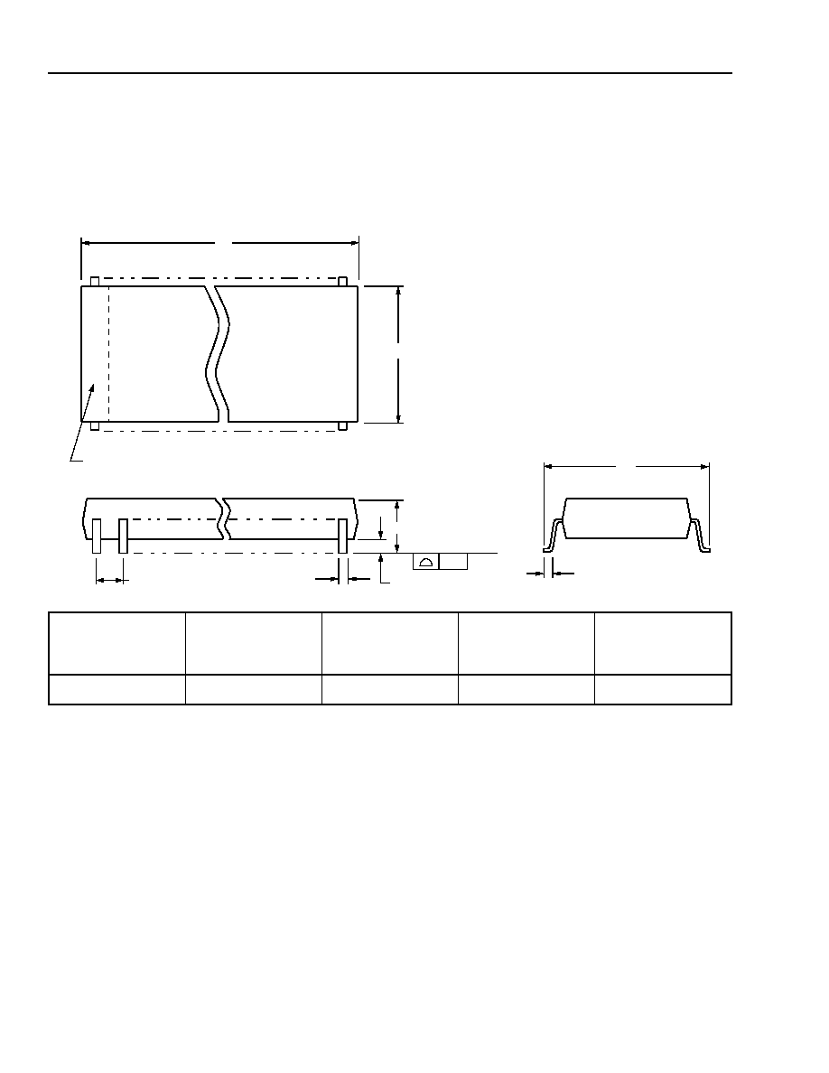
16-Pin, Plastic SOG (L7582AAE/BAE)
Note: The dimensions in this outline diagram are intended for informational purposes only. For detailed schematics
to assist your design efforts, please contact your Lucent Technologies Sales Representative.
5-4414 (F)
Number
of Pins
(N)
Maximum
Length
(L)
Maximum Width
Without Leads
(B)
Maximum Width
Including Leads
(W)
Maximum Height
Above Board
(H)
16
10.49
7.62
10.64
2.67
W
0.61
0.51 MAX
H
0.28 MAX
0.10
SEATING PLANE
1.27 TYP
N
L
B
1
PIN #1 IDENTIFIER ZONE

Lucent Technologies Inc.
15
Data Sheet
November 1999
L7582 Tip Ring Access Switch
Outline Diagrams
(continued)
16-Pin, Plastic DIP (L7582AC/BC)
Note: The dimensions in this outline diagram are intended for informational purposes only. For detailed schematics
to assist your design efforts, please contact your Lucent Technologies Sales Representative.
5-4410 (F)
Number
of Pins
(N)
Maximum
Length
(L)
Maximum Width
Without Leads
(B)
Maximum Width
Including Leads
(W)
Maximum Height
Above Board
(H)
16
20.57
6.48
7.87
5.08
W
H
0.58 MAX
2.54 TYP
0.38 MIN
SEATING PLANE
N
1
PIN #1 IDENTIFIER ZONE
L
B

Lucent Techn ologies I nc. re ser ves t he right t o make chan ges to the p roduct (s) or in formation c ontain ed he rein with out no tice. N
o liability i s assum ed as a res ult of t heir us e or applicatio n. No
rights unde r any pa tent acc ompa ny the s ale of a ny such p roduct (s) or in formation.
Copyright © 1999 Luce nt Technologie s Inc.
All Rights Res er ved
November 1999
DS00-051ALC (Replaces DS99-015ALC)
For additi onal info rm ation, contact your Microelectronics Group Acc ount Manager or the followi ng:
INTERNET: http://www.lucent.com/micro
E-MAIL: docmaster@micro.lucent.com
N. AMERICA:
Microelectronics Grou p, Lucent Technologies Inc., 555 Union Boul evard, Room 30L-15 P-BA, Allent own , PA 18103
1-800-372-2447, FAX 610-712-4106 (In CANADA: 1-800-553-2448, FAX 610-712-4106)
ASIA PACIFIC: Microelectronics Grou p, Lucent Technologies Singapore Pt e. Ltd., 77 Science Park Drive, #03-18 Cintech III , Singa p
ore 118256
Tel. (65) 778 8833, FAX (65) 777 7495
CHINA: Micr oelectronics Group, Lucent Techn ologies (China) Co., Lt d., A-F2, 23/F, Zao Fong Univers e Building, 1800 Zho ng Shan Xi
Road, Shang hai
200233 P. R. China Tel. (86) 21 6440 0468, ext. 316, FAX (86) 21 6440 0652
JAPAN: Micr oelectronics Group, Lucent Technolog ies Japan Ltd., 7-18, Higashi-Gotanda 2-chome, Shinagawa-ku, Tokyo 141, Japan
Tel. (81) 3 5421 1600, FAX (81) 3 5421 1700
EUROPE: Data Requ ests: MICROELECTRONICS GROUP DATALINE: Tel. (44) 7000 582 368, FAX (44) 1189 328 148
Technical Inquiries: GERMANY:
(49) 89 95086 0 (Munich), UNITED KINGDOM: (44) 1344 865 900 (Ascot),
FRANCE: (33) 1 40 83 68 00 (Paris), SWEDEN: (46) 8 594 607 00 (Sto ckholm), FINLAND : (358) 9 4354 2800 (Hels inki),
ITALY: (39) 02 6608131 (Milan), SPAIN: (34) 1 807 1441 (Madrid)
Data Sheet
November 1999
L7582 Tip Ring Access Switch
Ordering Information
*Devices o n tape an d reel must be ordered i n 1000-piece inc rement s.
Device Part No. Description Package Comcode
ATTL7582AAE Tip Ri ng Access Switch 16-pin SOG 107338543
ATTL7582AAE-TR* Tip Ri ng Access Switch 16-pin SO G (Tape & Reel) 107338576
ATTL7582AC Tip Ri ng Access Switch 16-pin DIP 107394181
ATTL7582BAE Tip Ri ng Access Switch 16-pin SOG 107394231
ATTL7582BAE-TR* Tip Ri ng Access Switch 16-pin SO G (Tape & Reel) 107394256
ATTL7582BC Tip Ri ng Access Switch 16-pin DIP 107394207