
Data Sheet
February 2001
L7583A/B/C/D Line Card Access Switch
Features
s
Small size/surface-mount packaging
s
Monolithic IC reliability
s
Low impulse noise
s
Make-before-break, break-before-make operation
s
Clean, bounce-free switching
s
Low, matched ON-resistance
s
Built-in current limiting, thermal shutdown, and
SLIC protection
s
5 V only operation, very low power consumption
s
Battery monitor, all OFF state upon loss of battery
s
No EMI
s
Latched logic level inputs, no driver circuitry
s
Only one external protector required
Applications
s
Central office
s
DLC
s
PBX
s
DAML
s
HFC/FITL
Description
The L7583A/B/C/D Line Card Access Switch is a
monolithic solid-state device providing the equivalent
switching functionality of three 2 form C switches.
The L7583 is designed to provide power ringing
access, line test access (test out), and SLIC test
access (test in) to tip and ring in central office, digital
loop carrier, private branch exchange, digitally added
main line, and hybrid fiber coax/fiber-in-the-loop ana-
log line card applications. An additional pair of solid-
state contacts are also available to provide access
for testing of the ringing generator.
The L7583A/B has seven states: the idle talk state
(line break switches closed, all other switches open),
the power ringing state (ringing access switches
closed, all other switches open), loop access state
(loop access switches closed, all switches open),
SLIC test state (test in switches closed, all other
switches open), simultaneous loop and SLIC
access state (loop and test in switches closed, all
others open), ringing generator test state (ring test
switches closed, all others open), and an all OFF
state. The seven states in the L7583A/B are also in
the L7583C/D, with an additional simultaneous test-
out and ring-test state, making the L7583C/D appro-
priate for digital loop carrier and other Bellcore TR-57
applications.
The L7583 offers break-before-make or make-
before-break switching, with simple logic level input
control. Because of the solid-state construction, volt-
age transients generated when switching into an
inductive ringing lead during ring cadence or ring trip
are minimized, possibly eliminating the need for
external zero cross switching circuitry. State control
is via logic level inputs, so no additional driver cir-
cuitry is required.
The line break switch is a linear switch that has
exceptionally low ON-resistance and an excellent
ON-resistance matching characteristic. The ringing
access switch has a breakdown voltage rating
>480 V which is sufficiently high, with proper protec-
tion, to prevent breakdown in the presence of a tran-
sient fault condition (i.e., passing the transient on to
the ringing generator).
Incorporated into the L7583Axx and L7583Cxx is a
diode bridge/SCR clamping circuit, current-limiting
circuitry, and a thermal shutdown mechanism to pro-
vide protection to the SLIC device and subsequent
circuitry during fault conditions. This is shown in Fig-
ure 1 as version A. Positive and negative lightning is
reduced by the current-limiting circuitry and steered
to ground via diodes and the integrated SCR. Power
cross is also reduced
by
the current-limiting and ther-
mal shutdown circuits.
2
2
Lucent Technologies Inc.
Data Sheet
February 2001
L7583A/B/C/D Line Card Access Switch
Description
(continued)
The L7583Bxx and L7583Dxx versions provide only an
integrated diode bridge along with current limiting and
thermal shutdown (see Figure 2 for version B). This will
cause positive faults to be directed to ground and neg-
ative faults to battery. In either polarity, faults are
reduced by the current-limit and/or thermal shutdown
mechanisms.
To protect the L7583 from an overvoltage fault condi-
tion, use of a secondary protector is required. The sec-
ondary protector must limit the voltage seen at the tip/
ring terminals to prevent the breakdown voltage of the
switches from being exceeded. To minimize stress on
the solid-state contacts, use of a foldback- or crowbar-
type secondary protector is recommended. With proper
choice of secondary protection, a line card using the
L7583 will meet all relevant ITU-T, LSSGR, FCC, or
UL
* protection requirements.
The L7583 operates off of a 5 V supply only. This gives
the device extremely low idle and active power dissipa-
tion and allows use with virtually any range of battery
voltage. This makes the L7583 especially appropriate
for remote power applications such as DAML or FOC/
FITL or other Bellcore TA 909 applications where
power dissipation is particularly critical.
A battery voltage is also used by the L7583, only as a
reference for the integrated protection circuit. The
L7583 will enter an all OFF state upon loss of battery.
During power ringing, to turn on and maintain the ON
state, the ring access switch and ring test switch will
draw a nominal 2 mA or 4 mA from the ring generator.
The L7583A/B/C/D device is packaged in a 24-pin,
plastic DIP (L7583AF/BF/CF/DF) and in a 28-pin,
plastic SOG (L7583AAJ/BAJ/CAJ/DAJ).
*
UL
is a registered trademark of Underwriters Laboratories, Inc.
Pin Information
12-2364.a (F)
Note: Shown with A/C version protection. The 24-pin DIP is avail-
able with either A/C or B/D version protection.
Figure 1. 24-Pin, Plastic DIP (600 mil)
12-2365.d (F)
Note: Shown with B/D version protection. The 28-pin SOG is avail-
able with either A/C or B/D version protection.
Figure 2. 28-Pin, Plastic SOG
24
23
22
21
20
19
18
17
16
15
14
13
1
2
3
4
5
6
7
V
BAT
R
BAT
R
LINE
NC
F
GND
NC
NC
T
LINE
V
DD
SW1
8
9
10
LATCH
R
RINGING
T
TESTout
SW2
SW3
SW4
SW5
SW7
SW9
SW8
SW10
SW6
T
TESTin
T
BAT
T
RINGING
NC
IN
TESTin
R
TESTout
R
TESTin
NC
11
12
IN
RING
D
GND
T
SD
IN
TESTout
CONTROL
LOGIC
SCR
AND
TRIP
CKT
28
27
26
25
24
23
22
20
19
18
17
21
16
15
1
2
3
4
5
6
7
8
V
BAT
R
BAT
R
LINE
NC
F
GND
NC
NC
T
LINE
V
DD
SW1
9
10
11
12
LATCH
R
RINGING
NC
SW2
SW3
SW4
SW5
SW7
SW9
SW8
SW10
SW6
T
TESTin
T
BAT
T
RINGING
T
TESTout
IN
TESTin
R
TESTout
R
TESTin
NC
13
14
IN
RING
D
GND
T
SD
IN
TESTout
NC
NC
NC
NC
CONTROL
LOGIC
Lucent Technologies Inc.
3
Data Sheet
February 2001
L7583A/B/C/D Line Card Access Switch
Pin Information
(continued)
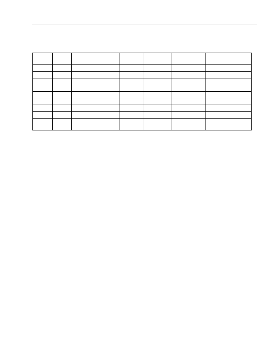
Table 1. Pin Descriptions
Absolute Maximum Ratings
Stresses in excess of the absolute maximum ratings can cause permanent damage to the device. These are abso-
lute stress ratings only. Functional operation of the device is not implied at these or any other conditions in excess
of those given in the operational sections of the data sheet. Exposure to absolute maximum ratings for extended
periods can adversely affect device reliability.
Table 2. Absolute Maximum Ratings
DIP SOG Symbol
Description
DIP
SOG
Symbol
Description
1
1
F
GND
Fault ground.
24
28
V
BAT
Battery voltage. Used as a ref-
erence for protection circuit.
2
2
NC
No connection.
23
27, 26
NC
No connection.
3
3, 4
NC
No connection.
22
25, 21
NC
No connection.
4
5
T
TESTin
Test (in) access on TIP.
21
24
R
TESTin
Test (in) access on RING.
5
6
T
BAT
Connect to TIP on SLIC side.
20
23
R
BAT
Connect to RING on SLIC
side.
6
7
T
LINE
Connect to TIP on line side.
19
22
R
LINE
Connect to RING on line side.
7
8
T
RINGING
Connect to return ground for ring-
ing generator.
18
20
R
RINGING
Connect to ringing generator.
8
10
T
TESTout
Test (out) access on TIP.
17
19
R
TESTout
Test (out) access on RING.
9
9, 11
NC
No connection.
16
18
LATCH
Data input control, active-high,
transparent low.
10
12
V
DD
5 V supply.
15
17
IN
TESTin
Logic level switch input control.
11
13
T
SD
Temperature shutdown pin. Can
be used as a logic level input or an
output. See Tables 16 and 17,
Truth Tables, and the Switching
Behavior section of this data sheet
for input pin description. As an
output flag, will read 5 V when the
device is in its operational mode
and 0 V in the thermal shutdown
mode. To disable the thermal shut-
down mechanism, tie this pin to
5 V (not recommended).
14
16
IN
RING
Logic level switch input control.
12
14
D
GND
Digital ground.
13
15
IN
TESTout
Logic level switch input control.
Parameter
Min
Max
Unit
Operating Temperature Range
≠40
110
∞C
Storage Temperature Range
≠40
150
∞C
Relative Humidity Range
5
95
%
Pin Soldering Temperature (t = 10 s max)
--
260
∞C
5 V Power Supply
--
7
V
Battery Supply
--
≠85
V
Logic Input Voltage
--
7
V
Input-to-output Isolation
--
330
V
Pole-to-pole Isolation
--
330
V
4
Lucent Technologies Inc.
Data Sheet
February 2001
L7583A/B/C/D Line Card Access Switch
Handling Precautions
Although protection circuitry has been designed into this device, proper precautions should be taken to avoid expo-
sure to electrostatic discharge (ESD) during handling and mounting. Lucent Technologies Microelectronics Group
employs a human-body model (HBM) and a charged-device model (CDM) for ESD-susceptibility testing and pro-
tection design evaluation. ESD voltage thresholds are dependent on the circuit parameters used to define the
model. No industry-wide standard has been adopted for CDM. However, a standard HBM (resistance = 1500
,
capacitance = 100 pF) is widely used and therefore can be used for comparison purposes. The HBM ESD thresh-
old presented here was obtained by using these circuit parameters.
Table 3. HBM ESD Threshold Voltage
Electrical Characteristics
T
A
= ≠40 ∞C to +85 ∞C, unless otherwise specified.
Minimum and maximum values are testing requirements. Typical values are characteristics of the device and are
the result of engineering evaluations. Typical values are for information purposes only and are not part of the test-
ing requirements.
Table 4. Power Supply Specifications
* V
BAT
is used only as a reference for internal protection circuitry. If V
BAT
rises above ≠10 V, the device will enter an all OFF state and remain in
this state until the battery voltage drops below ≠15 V.
Table 5. Test In Switches, 1 and 2
* Applied voltage is 100 Vp-p square wave at 100 Hz.
Device
Rating
L7583
1000 V
Supply
Min
Typ
Max
Unit
Supply
Min
Typ
Max
Unit
V
DD
4.5
5
5.5
V
V
BAT
*
≠19 --
≠72
V
Parameter
Test Condition
Measure
Min Typ Max
Unit
OFF-state Leakage Current:
+25 ∞C
+85 ∞C
≠40 ∞C
Vswitch (differential) = ≠320 V to Gnd
Vswitch (differential) = ≠60 V to +260 V
Vswitch (differential) = ≠330 V to Gnd
Vswitch (differential) = ≠60 V to +270 V
Vswitch (differential) = ≠310 V to Gnd
Vswitch (differential) = ≠60 V to +250 V
Iswitch
Iswitch
Iswitch
--
--
--
--
--
--
1
1
1
µA
µA
µA
ON-resistance:
+25 ∞C
+85 ∞C
≠40 ∞C
Iswitch (on) = ±5 mA, ±10 mA
Iswitch (on) = ±5 mA, ±10 mA
Iswitch (on) = ±5 mA, ±10 mA
V
ON
V
ON
V
ON
--
--
--
45
--
33
--
70
--
Isolation:
+25 ∞C
+85 ∞C
≠40 ∞C
Vswitch (both poles) = ±320 V,
Logic inputs = Gnd
Vswitch (both poles) = ±330 V,
Logic inputs = Gnd
Vswitch (both poles) = ±310 V,
Logic inputs = Gnd
Iswitch
Iswitch
Iswitch
--
--
--
--
--
--
1
1
1
µA
µA
µA
dV/dt Sensitivity*
--
--
--
200
--
V/µs

Lucent Technologies Inc.
5
Data Sheet
February 2001
L7583A/B/C/D Line Card Access Switch
Electrical Characteristics
(continued)
Table 6. Break Switches, 3 and 4
* This parameter is not tested in production. Choice of secondary protector should ensure this rating is not exceeded.
Applied voltage is 100 Vp-p square wave at 100 Hz.
Parameter
Test Condition
Measure
Min Typ Max Unit
OFF-state Leakage
Current:
+25 ∞C
+85 ∞C
≠40 ∞C
Vswitch (differential) = ≠320 V to Gnd
Vswitch (differential) = ≠60 V to +260 V
Vswitch (differential) = ≠330 V to Gnd
Vswitch (differential) = ≠60 V to +270 V
Vswitch (differential) = ≠310 V to Gnd
Vswitch (differential) = ≠60 V to +250 V
Iswitch
Iswitch
Iswitch
--
--
--
--
--
--
1
1
1
µA
µA
µA
ON-resistance:
+25 ∞C
+85 ∞C
≠40 ∞C
T
LINE
= ±10 mA, ±40 mA, T
BAT
= ≠2 V
T
LINE
= ±10 mA, ±40 mA, T
BAT
= ≠2 V
T
LINE
= ±10 mA, ±40 mA, T
BAT
= ≠2 V
V
ON
V
ON
V
ON
--
--
--
19.5
--
14.5
--
28
--
ON-resistance Match
Per ON-resistance test
condition of SW3, SW4
Magnitude
R
ON
SW3 ≠ R
ON
SW4
--
0.2
1.0
ON-state Voltage*
Iswitch = I
LIMIT
@ 50 Hz/60 Hz
V
ON
--
--
220
V
dc Current Limit:
+85 ∞C
≠40 ∞C
Vswitch (on) = ±10 V
Vswitch (on) = ±10 V
Iswitch
Iswitch
80
--
--
--
--
250
mA
mA
Dynamic Current Limit
(t = <0.5 µs)
Break switches in ON state; ringing
access switches OFF; apply ±1000 V at
10/1000 µs pulse; appropriate second-
ary protection in place
Iswitch
--
2.5
--
A
Isolation:
+25 ∞C
+85 ∞C
≠40 ∞C
Vswitch (both poles) = ±320 V,
Logic inputs = Gnd
Vswitch (both poles) = ±330 V,
Logic inputs = Gnd
Vswitch (both poles) = ±310 V,
Logic inputs = Gnd
Iswitch
Iswitch
Iswitch
--
--
--
--
--
--
1
1
1
µA
µA
µA
dV/dt Sensitivity
--
--
--
200
--
V/µs
6
Lucent Technologies Inc.
Data Sheet
February 2001
L7583A/B/C/D Line Card Access Switch
Electrical Characteristics
(continued)
Table 7. Ring Test Return Switch, 5
* Applied voltage is 100 Vp-p square wave at 100 Hz.
Table 8. Ringing Test Switch, 6
* Choice of secondary protector and series current-limit resistor should ensure these ratings are not exceeded.
Applied voltage is 100 Vp-p square wave at 100 Hz.
Parameter
Test Condition
Measure
Min
Typ Max Unit
OFF-state Leakage Current:
+25 ∞C
+85 ∞C
≠40 ∞C
Vswitch (differential) = ≠320 V to Gnd
Vswitch (differential) = ≠60 V to +260 V
Vswitch (differential) = ≠330 V to Gnd
Vswitch (differential) = ≠60 V to +270 V
Vswitch (differential) = ≠310 V to Gnd
Vswitch (differential) = ≠60 V to +250 V
Iswitch
Iswitch
Iswitch
--
--
--
--
--
--
1
1
1
µA
µA
µA
ON-resistance
Iswitch (on) = ±0 mA, ±10 mA
V
ON
--
50
100
Isolation:
+25 ∞C
+85 ∞C
≠40 ∞C
Vswitch (both poles) = ±320 V,
Logic inputs = Gnd
Vswitch (both poles) = ±330 V,
Logic inputs = Gnd
Vswitch (both poles) = ±310 V,
Logic inputs = Gnd
Iswitch
Iswitch
Iswitch
--
--
--
--
--
--
1
1
1
µA
µA
µA
dV/dt Sensitivity*
--
--
--
200
--
V/µs
Parameter
Test Condition
Measure
Min
Typ Max Unit
OFF-state Leakage Current:
+25 ∞C
+85 ∞C
≠40 ∞C
Vswitch (differential) = ≠60 V to +190 V
Vswitch (differential) = +60 V to ≠190 V
Vswitch (differential) = ≠60 V to +200 V
Vswitch (differential) = +60 V to ≠200 V
Vswitch (differential) = ≠60 V to +180 V
Vswitch (differential) = +60 V to ≠180 V
Iswitch
Iswitch
Iswitch
--
--
--
--
--
--
1
1
1
µA
µA
µA
ON-resistance
Iswitch (on) = ±70 mA, ±80 mA
V
ON
--
--
20
ON Voltage
Iswitch (on) = ±1 mA
--
--
--
1.5
V
Steady-state Current*
--
--
--
--
100
mA
Release Current
--
--
--
500
--
µA
Isolation:
+25 ∞C
+85 ∞C
≠40 ∞C
Vswitch (both poles) = ±320 V,
Logic inputs = Gnd
Vswitch (both poles) = ±330 V,
Logic inputs = Gnd
Vswitch (both poles) = ±310 V,
Logic inputs = Gnd
Iswitch
Iswitch
Iswitch
--
--
--
--
--
--
1
1
1
µA
µA
µA
dV/dt Sensitivity
--
--
--
200
--
V/µs
Lucent Technologies Inc.
7
Data Sheet
February 2001
L7583A/B/C/D Line Card Access Switch
Electrical Characteristics
(continued)
Table 9. Ring Return Switch, 7
* This parameter is not tested in production. Choice of secondary protector should ensure this rating is not exceeded.
Applied voltage is 100 Vp-p square wave at 100 Hz.
Table 10. Ringing Access Switch, 8
* At the time of publication of this data sheet, the current device design will be a nominal 4 mA. Devices are being redesigned to reduce this
current to less than 2 mA nominally. Consult your Lucent Technologies Microelectronics Group account executive for additional details.
Choice of secondary protector and series current-limit resistor should ensure these ratings are not exceeded.
Applied voltage is 100 Vp-p square wave at 100 Hz.
Parameter
Test Condition
Measure Min Typ Max Unit
OFF-state Leakage
Current:
+25 ∞C
+85 ∞C
≠40 ∞C
Vswitch (differential) = ≠320 V to Gnd
Vswitch (differential) = ≠60 V to +260 V
Vswitch (differential) = ≠330 V to Gnd
Vswitch (differential) = ≠60 V to +270 V
Vswitch (differential) = ≠310 V to Gnd
Vswitch (differential) = ≠60 V to +250 V
Iswitch
Iswitch
Iswitch
--
--
--
--
--
--
1
1
1
µA
µA
µA
dc Current Limit
Vswitch (on) = ±10 V
Iswitch
--
200
--
mA
Dynamic Current Limit
(t = <0.5 µs)
Break and loop switches in OFF state; ring return
switch ON; apply ±1000 V at 10/1000 µs pulse;
appropriate secondary protection in place
Iswitch
--
2.5
--
A
ON-resistance
Iswitch (on) = ±0 mA, ±10 mA
V
ON
--
--
100
ON-state Voltage*
Iswitch = I
LIMIT
@ 50 Hz/60 Hz
V
ON
--
--
130
V
Isolation:
+25 ∞C
+85 ∞C
≠40 ∞C
Vswitch (both poles) = ±320 V, Logic inputs = Gnd
Vswitch (both poles) = ±330 V, Logic inputs = Gnd
Vswitch (both poles) = ±310 V, Logic inputs = Gnd
Iswitch
Iswitch
Iswitch
--
--
--
--
--
--
1
1
1
µA
µA
µA
dV/dt Sensitivity
--
--
--
200
--
V/µs
Parameter
Test Condition
Measure Min
Typ Max Unit
OFF-state Leakage
Current:
+25 ∞C
+85 ∞C
≠40 ∞C
Vswitch (differential) = ≠255 V to +210 V
Vswitch (differential) = +255 V to ≠210 V
Vswitch (differential) = ≠270 V to +210 V
Vswitch (differential) = +270 V to ≠210 V
Vswitch (differential) = ≠245 V to +210 V
Vswitch (differential) = +245 V to ≠210 V
Iswitch
Iswitch
Iswitch
--
--
--
--
--
--
1
1
1
µA
µA
µA
ON Voltage
Iswitch (on) = ±1 mA
--
--
--
3
V
Ring Generator Cur-
rent During Ring
V
CC
= 5 V
IN
RING
= 1
IN
TESTin
= 0
IN
TESTout
= 0
I
RING-
SOURCE
--
*
--
mA
Steady-state Current
--
--
--
--
150
mA
Surge Current
--
--
--
--
2
A
Release Current
--
--
--
500
--
µA
ON-resistance
Iswitch (on) = ±70 mA, ±80 mA
V
ON
--
--
12
Isolation:
+25 ∞C
+85 ∞C
≠40 ∞C
Vswitch (both poles) = ±320 V, Logic inputs = Gnd
Vswitch (both poles) = ±330 V, Logic inputs = Gnd
Vswitch (both poles) = ±310 V, Logic inputs = Gnd
Iswitch
Iswitch
Iswitch
--
--
--
--
--
--
1
1
1
µA
µA
µA
dV/dt Sensitivity
--
--
--
200
--
V/µs

8
Lucent Technologies Inc.
Data Sheet
February 2001
L7583A/B/C/D Line Card Access Switch
Electrical Characteristics
(continued)
Table 11. Loop Access Switches, 9 and 10
* This parameter is not tested in production. Choice of secondary protector should ensure this rating is not exceeded.
Applied voltage is 100 Vp-p square wave at 100 Hz.
Parameter
Test Condition
Measure
Min Typ Max
Unit
OFF-state Leakage
Current:
+25 ∞C
+85 ∞C
≠40 ∞C
Vswitch (differential) = ≠320 V to Gnd
Vswitch (differential) = ≠60 V to +260 V
Vswitch (differential) = ≠330 V to Gnd
Vswitch (differential) = ≠60 V to +270 V
Vswitch (differential) = ≠310 V to Gnd
Vswitch (differential) = ≠60 V to +250 V
Iswitch
Iswitch
Iswitch
--
--
--
--
--
--
1
1
1
µA
µA
µA
ON-resistance:
+25 ∞C
+85 ∞C
≠40 ∞C
Iswitch (on) = ±5 mA, ±10 mA
Iswitch (on) = ±5 mA, ±10 mA
Iswitch (on) = ±5 mA, ±10 mA
Von
Von
Von
--
--
--
45
--
33
--
70
--
ON-state Voltage*
Iswitch = I
LIMIT
@ 50 Hz/60 Hz
V
ON
--
--
130
V
dc Current Limit:
+85 ∞C
≠40 ∞C
Vswitch (on) = ±10 V
Vswitch (on) = ±10 V
Iswitch
Iswitch
80
--
--
--
--
250
mA
mA
Dynamic Current Limit
(t = <0.5 µs)
Break switches in ON state; ringing access
switches OFF; apply ±1000 V at 10/1000 µs pulse;
appropriate secondary protection in place
Iswitch
--
2.5
--
A
Isolation:
+25 ∞C
+85 ∞C
≠40 ∞C
Vswitch (both poles) = ±320 V, Logic inputs = Gnd
Vswitch (both poles) = ±330 V, Logic inputs = Gnd
Vswitch (both poles) = ±310 V, Logic inputs = Gnd
Iswitch
Iswitch
Iswitch
--
--
--
--
--
--
1
1
1
µA
µA
µA
dV/dt Sensitivity
--
--
--
200
--
V/µs

Lucent Technologies Inc.
9
Data Sheet
February 2001
L7583A/B/C/D Line Card Access Switch
Electrical Characteristics
(continued)
Table 12. Additional Electrical Characteristics
* Temperature shutdown flag (T
SD
) will be high during normal operation and low during temperature shutdown state.
Zero Cross Current Turn Off
The ring access switch (SW8) is designed to turn off on the next zero current crossing after application of the
appropriate logic input control. This switch requires a current zero cross to turn off. Switch 8, once on, will remain
in the ON state (regardless of logic input) until a current zero cross. Therefore, to ensure proper operation of switch
8, this switch should be connected, via proper impedance, to the ringing generator or some other ac source. Do
not attempt to switch pure dc with switch 8. The ringing test access switch, SW6, also has similar characteristics to
switch 8 and should also only be used to switch signals with zero current crossings. For a detailed explanation of
the operation of switches 6 and 8, please refer to the
An Introduction to L758X Series of Line Card Access
Switches
Application Note.
Parameter
Test Condition
Measure
Min
Typ
Max Unit
Digital Input Characteristics:
Input Low Voltage
--
--
--
--
1.5
V
Input High Voltage
--
--
3.5
--
--
V
Input Leakage Current (high)
V
DD
= 5.5 V, V
BAT
= ≠75 V,
Vlogicin = 5 V
llogicin
--
--
1
µA
Input Leakage Current (low)
V
DD
= 5.5 V, V
BAT
= ≠75 V,
Vlogicin = 0 V
llogicin
--
--
1
µA
Power Requirements:
Power Dissipation
V
DD
= 5 V, V
BAT
= ≠48 V,
idle/talk state or all OFF state,
ringing state or access state
I
DD
, I
BAT
I
DD
--
--
3
6
5
10
mW
mW
V
DD
Current
V
DD
= 5 V,
idle/talk state or all OFF state,
ringing state or access state
I
DD
I
DD
--
--
560
0.750
900
1.9
µA
mA
V
BAT
Current
V
BAT
= ≠48 V,
idle/talk state or all OFF state,
ringing state or access state
I
BAT
I
BAT
--
--
4
4
10
10
µA
µA
Digital Input Characteristics:
Input Low Voltage
--
--
--
--
1.5
V
Input High Voltage
--
--
3.5
--
--
V
Input Leakage Current (high)
V
DD
= 5.5 V, V
BAT
= ≠58 V,
Vlogicin = 5 V
llogicin
--
--
1
µA
Input Leakage Current (low)
V
DD
= 5.5 V, V
BAT
= ≠58 V,
Vlogicin = 0 V
llogicin
--
--
1
µA
Temperature Shutdown Requirements*:
Shutdown Activation Temperature
--
--
110
125
150
∞C
Shutdown Circuit Hysteresis
--
--
10
--
25
∞C

10
10
Lucent Technologies Inc.
Data Sheet
February 2001
L7583A/B/C/D Line Card Access Switch
Switching Behavior
When switching from the power ringing state to the
idle/talk state, via simple logic level input control, the
L7583 is able to provide control with respect to the tim-
ing when the ringing access contacts are released rela-
tive to the state of the line break contacts.
Make-before-break operation occurs when the line
break switch contacts are closed (or made) before the
ringing access switch contact is opened (or broken).
Break-before-make operation occurs when the ringing
access contact is opened before the line break switch
contacts are closed.
Using the logic level input pins RING, TESTin, and
TESTout, either make-before-break or break-before-
make operation of the L7583 is easily achieved. The
logic sequences for either mode of operation are given
in Table 13 and Table 14. See the Truth Tables (Table
16 and Table 17) for an explanation of logic states.
When using an L758X in the make-before-break mode,
during the ring-to-idle transition, for a period of up to
one-half the ringing frequency, the ring break switch
and the pnpn-type ring access switch can both be in
the ON state. This is the maximum time after the logic
signal at IN
RING
has transitioned that the ring access
switch is waiting for the next zero current cross, so it
can close. During this interval, current that is limited to
the dc break switch current-limit value will be source
from the ring node of the SLIC.
This current is presented to the internal protection cir-
cuit. If the SCR-type protector is used (A or C codes), if
by random probability the ring-to-idle transition occurs
during a portion of the ring cycle when the ringing volt-
age exceeds the protection circuit SCR turn-on volt-
age, and if current in excess of the SCR's turn-on
current is also available, the SCR may turn on. Once
the SCR is triggered on, if the SLIC is capable of sup-
plying current in excess of the holding current, the SCR
may be latched on by the SLIC.
The probability of this event depends on the character-
istics of the given SLIC and of the holding current of the
L7583 A or C device. The SCR hold current distribution
is designed to be safely away from the test limit of
80 mA. The higher the distribution, the lower the proba-
bility of the latch.
If this situation is of concern for a given board design,
either use the A or C series device in the break-before-
make mode (eliminates the original 25 ms current
pulse) or use a B or D series device (eliminates the
SCR).
Table 13. Make-Before-Break Operation
RING TESTin TESTout
T
SD
State
Timing
Break
Switches
3 & 4
Ring
Return
Switch 7
Ring
Access
Switch 8
All Other
Access
Switches
5 V
0 V
0 V
Float
Power
Ringing
--
Open
Closed
Closed
Open
0 V
0 V
0 V
Float
Make-
before-
break
SW8 waiting for next
zero current crossing
to turn off maximum
time--one-half of
ringing. In this transi-
tion state, current
that is limited to the
dc break switch cur-
rent-limit value will be
sourced from the ring
node of the SLIC.
Closed
Open
Closed
Open
0 V
0 V
0 V
Float
Idle/Talk Zero cross current
has occurred.
Closed
Open
Open
Open

Data Sheet
February 2001
Lucent Technologies Inc.
11
L7583A/B/C/D Line Card Access Switch
Switching Behavior
(continued)
Table 14. Break-Before-Make Operation
Notes:
Break-before-make operation can be achieved using T
SD
as an input. In lines two and three of Table 14, instead of using the logic input pins to
force the all OFF state, force T
SD
to ground. This will override the logic inputs and also force the all OFF state. Hold this state for 25 ms. During
this 25 ms all OFF state, toggle the inputs from 10 (ringing state) to 00 (idle/talk state). After 25 ms, release T
SD
to return switch control to the
input pins which will set the idle talk state.
When using the L7583A/B/C/D in this mode, forcing T
SD
to ground will override the INPUT pins and force an all OFF state. Setting T
SD
to
5 V will allow switch control via the logic INPUT pins. However, setting T
SD
to 5 V will also disable the thermal shutdown mechanism. This is not
recommended. Therefore, to allow switch control via the logic INPUT pins, allow T
SD
to float.
Thus, when using T
SD
as an input, the two recommended states are 0 (overrides logic input pins and forces all OFF state) and float (allows
switch control via logic input pins and thermal shutdown mechanism is active). This may require use of an open-collector buffer.
Also note that T
SD
operation in L7583 is different than T
SD
operation of the L7581, where application of 5 V does not disable the thermal shut-
down mechanism.
INPUT TESTin TESTout
T
SD
State
Timing
Break
Switches
3 & 4
Ring
Return
Switch
7
Ring
Access
Switch
8
All Other
Switches
5 V
0 V
0 V
Float
Power
Ringing
--
Open
Closed
Closed
Open
5 V
0 V
5 V
Float
All Off
Hold this state for
25 ms. SW8 waiting
for zero current to turn
off.
Open
Open
Closed
Open
5 V
0 V
5 V
Float
All Off
Zero current has
occurred and SW8 has
opened.
Open
Open
Open
Open
0 V
0 V
0 V
Float
Idle/Talk
Release break
switches.
Closed
Open
Open
Open
Power Supplies
Both the 5 V and battery supply are brought onto the
L7583. The L7583 requires only the 5 V supply for
switch operation; that is, state control is powered exclu-
sively off of the 5 V supply. Because of this, the L7583
offers extremely low power dissipation, both in the idle
and active states.
The battery voltage is not used for switch state control.
The battery is used as a reference voltage by the inte-
grated secondary protection circuit. When the voltage
at T
BAT
or R
BAT
drops 2 V to 4 V below the battery, the
integrated SCR will trigger, thus preventing fault-
induced overvoltage situations at the T
BAT
/R
BAT
nodes.
Loss of Battery Voltage
As an additional protection feature, the L7583 monitors
the battery voltage. Upon loss of battery voltage, the
L7583 will automatically enter an all OFF state and
remain in that state until the battery voltage is restored.
The L7583 is designed such that the device will enter
the all OFF state if the battery rises above ≠10 V and
will remain off until the battery drops below ≠15 V.
Monitoring the battery for the automatic shutdown fea-
ture will draw a small current from the battery, typically
4 µA. This will add slightly to the overall power dissipa-
tion of the device.
Impulse Noise
Using the L7583 will minimize and possibly eliminate
the contribution to the overall system impulse noise
that is associated with ringing access switches.
Because of this characteristic of the L7583, it may not
be necessary to incorporate a zero cross switching
scheme. This ultimately depends upon the characteris-
tics of the individual system and is best evaluated at
the board level.

12
12
Lucent Technologies Inc.
Data Sheet
February 2001
L7583A/B/C/D Line Card Access Switch
Protection
Integrated SLIC Protection
Diode Bridge/SCR
In the L7583Axx and the L7583Cxx versions, protec-
tion to the SLIC device or other subsequent circuitry is
provided by a combination of current-limited break
switches, a diode bridge/SCR clamping circuit, and a
thermal shutdown mechanism. In the L7583Bxx and
the L7583Dxx versions, protection to the SLIC device
or other subsequent circuitry is provided by a combina-
tion of current-limited break switches, a diode bridge,
and a thermal shutdown mechanism.
In both protection versions, during a positive lightning
event, fault current is directed to ground via steering
diodes in the diode bridge. Voltage is clamped to a
diode drop above ground. In the A version, negative
lightning causes the SCR to conduct when the voltage
goes 2 V to 4 V more negative than the battery. Fault
currents are then directed to ground via the SCR and
steering diodes in the diode bridge.
Note that for the SCR to foldback or crowbar, the ON
voltage (see Table 14) of the SCR must be less nega-
tive than the battery reference voltage. If the battery
voltage is less negative than the SCR ON voltage, the
SCR will conduct fault currents to ground; however, it
will not crowbar.
In the B/D version, negative lightning is directed to bat-
tery via steering diodes in the diode bridge.
For power cross and power induction faults, in both
protection versions, the positive cycle of the fault is
clamped a diode drop above ground and fault currents
steered to ground. In the A/C version, the negative
cycle will cause the SCR to trigger when the voltage
exceeds the battery reference voltage by 2 V to 4 V.
When the SCR triggers, fault current is steered to
ground. In the B/D version, the negative cycle of the
power cross is steered to battery.
Current Limiting
During a lightning event, the current that is passed
through the break switches and presented to the inte-
grated protection circuit and subsequent circuitry is lim-
ited by the dynamic current-limit response of the break
switches (assuming idle/talk state). When the voltage
seen at the T
LINE
/R
LINE
nodes is properly clamped by
an external secondary protector, upon application of a
1000 V, 10 x 1000 pulse (LSSGR lightning), the current
seen at the T
BAT
/R
BAT
nodes will typically be a pulse of
magnitude 2.5 A and duration less than 0.5 µs.
During a power cross event, the current that is passed
through the break switches and presented to the inte-
grated protection circuit and subsequent circuitry is lim-
ited by the dc current-limit response of the break
switches (assuming idle/talk state). The dc current limit
is specified over temperature between 100 mA and
250 mA. Note that the current-limit circuitry has a nega-
tive temperature coefficient. Thus, if the device is sub-
jected to an extended power cross, the value of current
seen at T
BAT
/R
BAT
will decrease as the device heats
due to the fault current. If sufficient heating occurs, the
temperature shutdown mechanism will activate and the
device will enter an all off mode.
Temperature Shutdown Mechanism
When the device temperature reaches a minimum of
110 ∞C, the thermal shutdown mechanism will activate
and force the device into an all OFF state, regardless
of the logic input pins. Pin T
SD
, when used as an out-
put, will read 0 V when the device is in the thermal
shutdown mode and +V
DD
during normal operation.
During a lightning event, due to the relatively short
duration, the thermal shutdown will not typically acti-
vate.
During an extended power cross, the device tempera-
ture will rise and cause the device to enter the thermal
shutdown mode. This forces an all off mode, and the
current seen at T
BAT
/R
BAT
drops to zero. Once in the
thermal shutdown mode, the device will cool and exit
the thermal shutdown mode, thus reentering the state it
was in prior to thermal shutdown. Current, limited to the
dc current-limit value, will again begin to flow and
device heating will begin again. This cycle of entering
and exiting thermal shutdown will last as long as the
power cross fault is present. The frequency of entering
and exiting thermal shutdown will depend on the mag-
nitude of the power cross. If the magnitude of the
power cross is great enough, the external secondary
protector may trigger shunting all current to ground.
In the L7583, the thermal shutdown mechanism can be
disabled by forcing the T
SD
pin to +V
DD
. This functional-
ity is different from the L7581, whose thermal shutdown
mechanism cannot be disabled.
Electrical specifications relating to the integrated over-
voltage clamping circuit are outlined in Table 15.
Lucent Technologies Inc.
13
Data Sheet
February 2001
L7583A/B/C/D Line Card Access Switch
Protection
(continued)
Integrated SLIC Protection
(continued)
External Secondary Protector
With the above integrated protection features, only one
overvoltage secondary protection device on the loop
side of the L7583 is required. The purpose of this
device is to limit fault voltages seen by the L7583 so as
not to exceed the breakdown voltage or input-output
isolation rating of the device. To minimize stress on the
L7583, use of a foldback- or crowbar-type device is rec-
ommended. A detailed explanation and design equa-
tions on the choice of the external secondary protection
device are given in the
An Introduction to L758X Series
of Line Card Access Switches
Application Note. Basic
design equations governing the choice of external sec-
ondary protector are given below.
s
|
V
BATmax
| +
|
V
breakovermax
|
<
|
V
breakdownmin(break)
|
s
|
V
ringingpeakmax
|
+
|
V
BATmax
|
+
|
V
breakovermax
|
<
|
V
breakdownmin(ring)
|
s
|
V
ringingpeakmax
|
+
|
V
BATmax
|
<
|
V
breakovermin
|
where:
V
BATmax
--Maximum magnitude of battery voltage.
V
breakovermax
--Maximum magnitude breakover voltage
of external secondary protector.
V
breakovermin
--Minimum magnitude breakover voltage
of external secondary protector.
V
breakdownmin(break)
--Minimum magnitude breakdown
voltage of L7583 break switch.
V
breakdownmin(ring)
--Minimum magnitude breakdown
voltage of L7583 ring access switch.
V
ringingpeakmax
--Maximum magnitude peak voltage of
ringing signal.
Series current-limiting fused resistors or PTCs should
be chosen so as not to exceed the current rating of the
external secondary protector. Refer to the manufac-
turer's data sheet for requirements.
Table 15. Electrical Specifications, Protection Circuitry
* Previous versions of this data sheet specified a Trigger Current of 50 mA minimum. Trigger Current is defined as the minimum current drawn
from tip and ring to turn on the SCR. The specification in this data sheet is Gate Trigger Current, which is defined as the maximum current
that can flow into the battery before the SCR turns on.
Typical at 25 ∞C.
Twice ± dynamic current limit of break switches.
ß In some instances, the typical ON-state voltage can range as low as ≠25 V.
Parameters Related to Diodes (in Diode Bridge)
Parameter
Test Condition
Measure
Min
Typ
Max
Unit
Voltage Drop @ Continuous Cur-
rent (50 Hz/60 Hz)
Apply ±dc current limit
of break switches
Forward
Voltage
--
--
3
V
Voltage Drop @ Surge
Current
Apply ±dynamic cur-
rent limit of break
switches
Forward
Voltage
--
5
--
V
Parameters Related to Protection SCR
Surge Current
--
--
--
--
A
Gate Trigger Current*
--
--
--
25
50
mA
Gate Trigger Current
Tempera-
ture Coefficient
--
--
--
≠0.5
--
%/∞C
Hold Current
--
--
70
--
--
mA
Gate Trigger Voltage
Trigger current
--
V
BAT
≠ 4
--
V
BAT
≠ 2
V
Reverse Leakage Current
V
BAT
--
--
--
1.0
µA
ON-State Voltage
ß
0.5 A, t = 0.5 µs
2.0 A, t = 0.5 µs
V
ON
--
--
--
≠3
≠5
--
--
V
V
14
14
Lucent Technologies Inc.
Data Sheet
February 2001
L7583A/B/C/D Line Card Access Switch
Typical Performance Characteristics
12-2309.f (F)
Figure 3. Protection Circuit A/C Version
12-2309.b (F)
Figure 4. Protection Circuit B/D Version
12-2311 (F)
Figure 5. Switches 1--5, 7, 9, 10
12-2312 (F)
Figure 6. Switches 6, 8
V
BAT
<1
µ
A
3 V
dc CURRENT-LIMIT
BREAK SWITCHES
V
BAT
≠ 2
V
ON
50 mA
dc CURRENT LIMIT
(OF BREAK SWITCHES)
V
BAT
≠ 4
I
H
V
BAT
<1
µ
A
3 V
dc CURRENT-LIMIT
BREAK SWITCHES
dc CURRENT LIMIT
(OF BREAK SWITCHES)
V
BAT
≠ 3
+I
+V
≠1.5 V
2/3 R
ON
CURRENT
LIMITING
≠I
≠V
CURRENT
LIMITING
I
LIMIT
I
LIMIT
R
ON
1.5 V
2/3 R
ON
R
ON
+I
+V
OS
+V
R
ON
≠V
OS
≠I
≠V
Lucent Technologies Inc.
15
Data Sheet
February 2001
L7583A/B/C/D Line Card Access Switch
Application
12-2366.d (F)
Figure 7. Typical LCAS Application, Idle, or Talk State Shown (A/C-Type Internal Protection Shown)
CROWBAR
PROTECTION
R1
R2
TIP
RING
SW9
SW8
SW3 BREAK
BREAK SW4
RING
TIP
BATTERY
FEED
RING
GENERATOR
BATTERY
SCR
AND
TRIP
CKT
V
BAT
(REFERENCE)
RINGING
SW1
SW7
TEST OUT
RINGING
RETURN
TEST RETURN
SW5
TEST IN
SW10
TEST OUT
RINGING
ACCESS
RINGING TEST
SW6
SW2
TEST IN

16
Lucent Technologies Inc.
Data Sheet
February 2001
L7583A/B/C/D Line Card Access Switch
Application
(continued)
Table 16. Truth Table for L7583A/B
1. If T
SD
= 5 V, the thermal shutdown mechanism is disabled. If T
SD
is floating, the thermal shutdown mechanism is active.
2. Forcing T
SD
to ground overrides the logic input pins and forces an all OFF state.
3. Idle/Talk state.
4. TESTout state.
5. TESTin state
6. Power ringing state.
7. Ringing generator test state.
8. Simultaneous TESTout and TESTin state.
9. All OFF state.
A parallel in/parallel out data latch is integrated into the L7583A/B. Operation of the data latch is controlled by the
logic level input pin LATCH. The data input to the latch is the INPUT pin of the L7583A/B, and the output of the data
latch is an internal node used for state control.
When the LATCH control pin is at logic 0, the data latch is transparent and data control signals flow directly from
INPUT, through the data latch to state control. Any changes in INPUT will be reflected in the state of the switches.
When the LATCH control pin is at logic 1, the data latch is active--the L7583A/B will no longer react to changes at
the INPUT control pin. The state of the switches is now latched; that is, the state of the switches will remain as they
were when the LATCH input transitioned from logic 0 to logic 1. The switches will not respond to changes in INPUT
as long as LATCH is held high.
Note that the T
SD
input is not tied to the data latch. T
SD
is not affected by the LATCH input. T
SD
input will override
state control via INPUT and LATCH.
IN
RING
IN
TESTin
IN
TESTout
T
SD
TESTin
Switches
Break
Switches
Ring Test
Switches
Ring
Switches
TESTout
Switches
0 V
0 V
0 V
5 V/Float
1
Off
On
Off
Off
Off
3
0 V
0 V
5 V
5 V/Float
1
Off
Off
Off
Off
On
4
0 V
5 V
0 V
5 V/Float
1
On
Off
Off
Off
Off
5
5 V
0 V
0 V
5 V/Float
1
Off
Off
Off
On
Off
6
5 V
5 V
0 V
5 V/Float
1
Off
Off
On
Off
Off
7
0 V
5 V
5 V
5 V/Float
1
On
Off
Off
Off
On
8
5 V
0 V
5 V
5 V/Float
1
Off
Off
Off
Off
Off
9
5 V
5 V
5 V
5 V/Float
1
Off
Off
Off
Off
Off
9
Don't
Care
Don't
Care
Don't
Care
0 V
2
Off
Off
Off
Off
Off
9
Lucent Technologies Inc.
17
Data Sheet
February 2001
L7583A/B/C/D Line Card Access Switch
Application
(continued)
Table 17. Truth Table for L7583C/D
1.
If T
SD
= 5 V, the thermal shutdown mechanism is disabled. If T
SD
is floating, the thermal shutdown mechanism is active.
2.
Forcing T
SD
to ground overrides the logic input pins and forces an all OFF state.
3.
Idle/Talk state.
4.
TESTout state.
5.
TESTin state.
6.
Power ringing state.
7.
Ringing generator test state.
8.
Simultaneous TESTout and TESTin state.
9.
All OFF state.
10. Simultaneous TESTout--Ring Test state.
A parallel in/parallel out data latch is integrated into the L7583C/D. Operation of the data latch is controlled by the
logic level input pin LATCH. The data input to the latch is the INPUT pin of the L7583C/D and the output of the data
latch is an internal node used for state control.
When the LATCH control pin is at logic 0, the data latch is transparent and data control signals flow directly from
INPUT, through the data latch to state control. Any changes in INPUT will be reflected in the state of the switches.
When the LATCH control pin is at logic 1, the data latch is active; the L7583C/D will no longer react to changes at
the INPUT control pin. The state of the switches is now latched; that is, the state of the switches will remain as they
were when the LATCH input transitioned from logic 0 to logic 1. The switches will not respond to changes in INPUT
as long as LATCH is held high.
Note that the T
SD
input is not tied to the data latch. T
SD
is not affected by the LATCH input. T
SD
input will override
state control via INPUT and LATCH.
IN
RING
IN
TESTin
IN
TESTout
T
SD
TESTin
Switches
Break
Switches
Ring Test
Switches
Ring
Switches
TESTout
Switches
0 V
0 V
0 V
5 V/Float
1
Off
On
Off
Off
Off
3
0 V
0 V
5 V
5 V/Float
1
Off
Off
Off
Off
On
4
0 V
5 V
0 V
5 V/Float
1
On
Off
Off
Off
Off
5
5 V
0 V
0 V
5 V/Float
1
Off
Off
Off
On
Off
6
5 V
5 V
0 V
5 V/Float
1
Off
Off
On
Off
Off
7
0 V
5 V
5 V
5 V/Float
1
On
Off
Off
Off
On
8
5 V
0 V
5 V
5 V/Float
1
Off
Off
Off
Off
Off
9
5 V
5 V
5 V
5 V/Float
1
Off
Off
On
Off
On
10
Don't
Care
Don't
Care
Don't
Care
0 V
2
Off
Off
Off
Off
Off
9
18
Lucent Technologies Inc.
Data Sheet
February 2001
L7583A/B/C/D Line Card Access Switch
Outline Diagrams
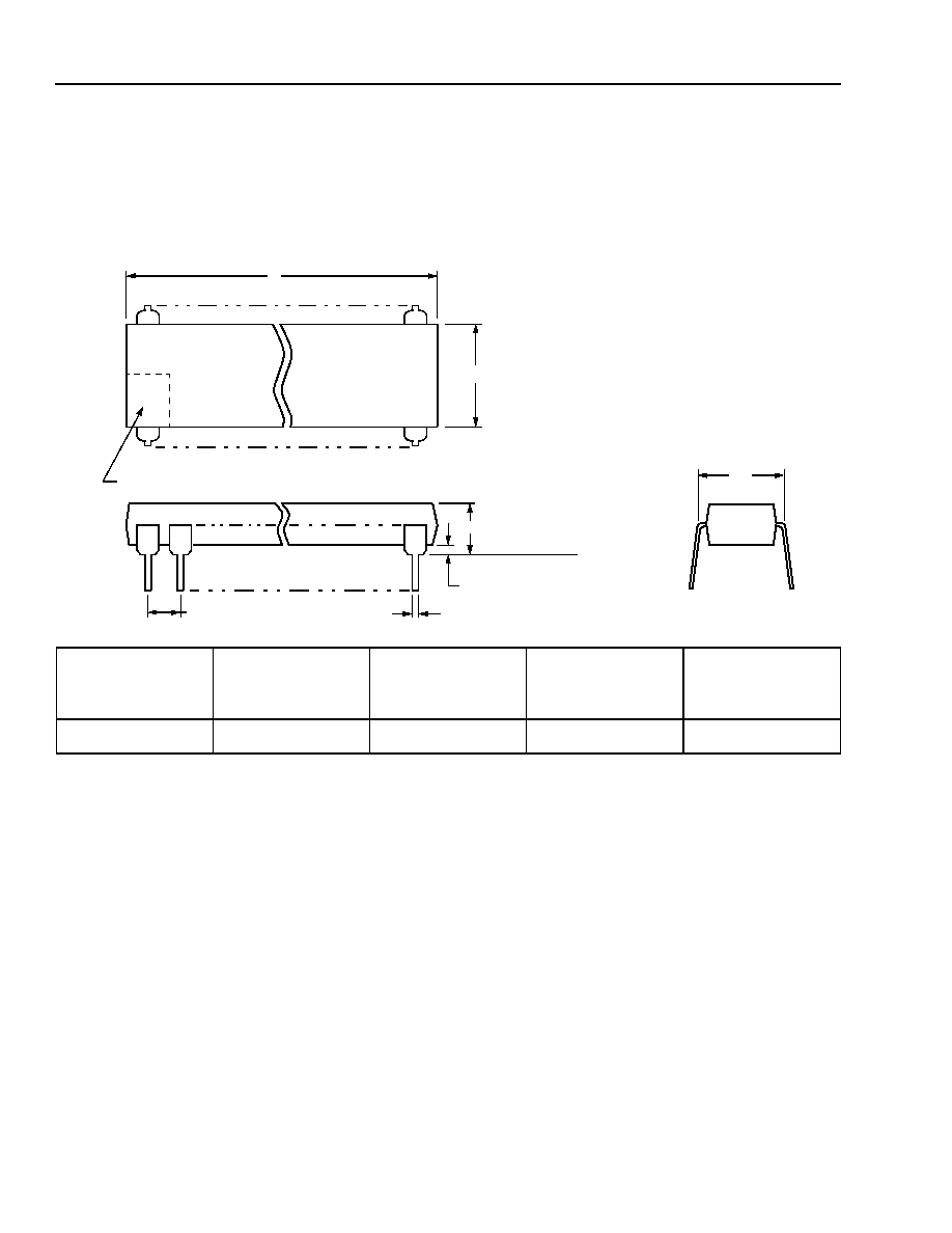
24-Pin, Plastic DIP (600 mil)
Note: The dimensions in this outline diagram are intended for informational purposes only. For detailed schematics
to assist your design efforts, please contact your Lucent Technologies Sales Representative.
5-4410 (F)
Number
of Pins
(N)
Maximum
Length
(L)
Maximum Width
Without Leads
(B)
Maximum Width
Including Leads
(W)
Maximum Height
Above Board
(H)
24
32.26
13.97
15.49
5.49
W
H
0.58 MAX
2.54 TYP
0.38 MIN
SEATING PLANE
N
1
PIN #1 IDENTIFIER ZONE
L
B
Lucent Technologies Inc.
19
Data Sheet
February 2001
L7583A/B/C/D Line Card Access Switch
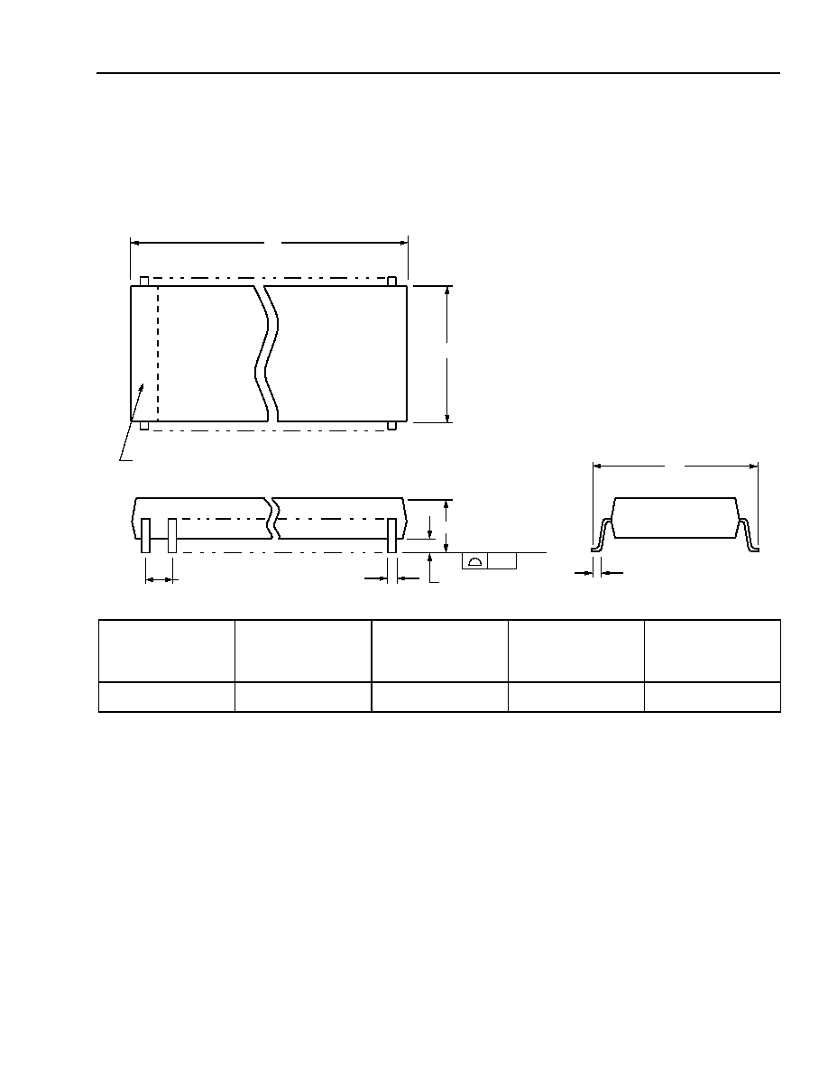
Outline Diagrams
(continued)
28-Pin, Plastic SOG
Note: The dimensions in this outline diagram are intended for informational purposes only. For detailed schemat-
ics to assist your design efforts, please contact your Lucent Technologies Sales Representative.
5-4414 (F)
Number
of Pins
(N)
Maximum Length
(L)
Maximum Width
Without Leads
(B)
Maximum Width
Including Leads
(W)
Maximum Height
Above Board
(H)
28
18.11
7.62
10.64
2.67
W
0.61
0.51 MAX
H
0.28 MAX
0.10
SEATING PLANE
1.27 TYP
N
L
B
1
PIN #1 IDENTIFIER ZONE
Data Sheet
February 2001
L7583A/B/C/D Line Card Access Switch
Lucent Technologies Inc. reserves the right to make changes to the product(s) or information contained herein without notice. N o liability is assumed as a result of their use or application. No
rights under any patent accompany the sale of any such product(s) or information.
Copyright © 2001 Lucent Technologies Inc.
All Rights Reserved
February 2001
DS01-111ALC (Replaces DS00-052ALC)
For additional information, contact your Microelectronics Group Account Manager or the following:
INTERNET: http://www.lucent.com/micro
E-MAIL: docmaster@micro.lucent.com
N. AMERICA:
Microelectronics Group, Lucent Technologies Inc., 555 Union Boulevard, Room 30L-15P-BA, Allentown, PA 18109-3286
1-800-372-2447, FAX 610-712-4106 (In CANADA: 1-800-553-2448, FAX 610-712-4106)
ASIA PACIFIC: Microelectronics Group, Lucent Technologies Singapore Pte. Ltd., 77 Science Park Drive, #03-18 Cintech III, Singapore 118256
Tel. (65) 778 8833, FAX (65) 777 7495
CHINA: Microelectronics Group, Lucent Technologies (China) Co., Ltd., A-F2, 23/F, Zao Fong Universe Building, 1800 Zhong Shan Xi Road, Shanghai
200233 P. R. China Tel. (86) 21 6440 0468, ext. 325, FAX (86) 21 6440 0652
JAPAN: Microelectronics Group, Lucent Technologies Japan Ltd., 7-18, Higashi-Gotanda 2-chome, Shinagawa-ku, Tokyo 141, Japan
Tel. (81) 3 5421 1600, FAX (81) 3 5421 1700
EUROPE: Data Requests: MICROELECTRONICS GROUP DATALINE: Tel. (44) 7000 582 368, FAX (44) 1189 328 148
Technical Inquiries: GERMANY: (49) 89 95086 0 (Munich), UNITED KINGDOM: (44) 1344 865 900 (Ascot),
FRANCE: (33) 1 40 83 68 00 (Paris), SWEDEN: (46) 8 594 607 00 (Stockholm), FINLAND: (358) 9 3507670 (Helsinki),
ITALY: (39) 02 6608131 (Milan), SPAIN: (34) 1 807 1441 (Madrid)
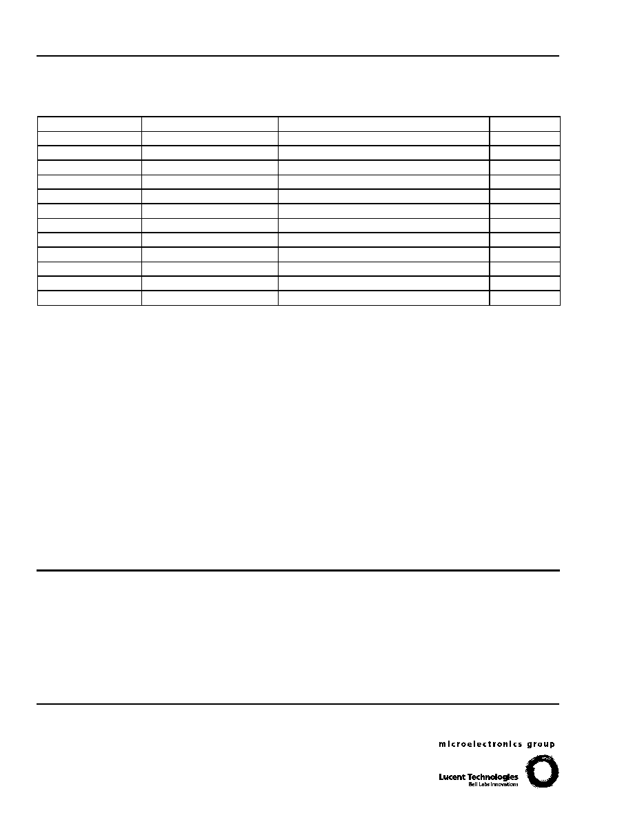
Ordering Information
*Devices on tape and reel must be ordered in 1000-piece increments.
Device Part No. Description Package Comcode
ATTL7583AAJ -D Line Card Access Switch 28-Pin SOG (Dry-bagged) 107338626
ATTL7583AAJ-DT* Line Card Access Switch 28-Pin SOG (Tape & Reel, Dry-bagged) 107338659
ATTL7583AF Line Card Access Switch 24-Pin DIP 107338592
ATTL7583BAJ-D Line Card Access Switch 28-Pin SOG (Dry-bagged) 107394355
ATTL7583BAJ-DT* Line Card Access Switch 28-Pin SOG (Tape & Reel, Dry-bagged) 107411563
ATTL7583BF Line Card Access Switch 24-Pin DIP 107394306
ATTL7583CAJ-D Line Card Access Switch 28-Pin SOG (Dry-bagged) 107602229
ATTL7583CAJ-DT* Line Card Access Switch 28-Pin SOG (Tape & Reel, Dry-bagged) 107602245
ATTL7583CF Line Card Access Switch 24-Pin DIP 107602278
ATTL7583DAJ-D Line Card Access Switch 28-Pin SOG (Dry-bagged) 107602328
ATTL7583DAJ-DT* Line Card Access Switch 28-Pin SOG (Tape & Reel, Dry-bagged) 107602344
ATTL7583DF Line Card Access Switch 24-Pin DIP 107602377