 | –≠–ª–µ–∫—Ç—Ä–æ–Ω–Ω—ã–π –∫–æ–º–ø–æ–Ω–µ–Ω—Ç: BPPGA16NB | –°–∫–∞—á–∞—Ç—å:  PDF PDF  ZIP ZIP |

Data Sheet
January 1999
Quad Differential Drivers
BDG1A, BDP1A, BDGLA, BPNGA, BPNPA, and BPPGA
Features
s
Pin-equivalent to the general-trade 26LS31 device,
with improved speed, reduced power consumption,
and significantly lower levels of EMI
s
Four line drivers per package
s
Meets ESDI standards
s
2.0 ns maximum propagation delay
s
Single 5.0 V
±
10% supply
s
Operating temperature range:
-
40 ∞C to +125 ∞C
(wider than the 41 Series)
s
400 Mbits/s maximum data rate
s
Logic to convert TTL input logic levels to differen-
tial, pseudo-ECL output logic levels
s
No line loading when V
CC
= 0 (BDG1A, BDP1A
only)
s
High output driver for 50
loads
s
<0.2 ns output skew (typical)
s
On-chip 220
loads available
s
Third-state outputs available
s
Surge-protection to ±60 V for 10 ms available
(BPNGA, BPNPA, BPPGA)
s
Available in four package types
s
ESD performance better than the 41 Series
s
Lower power requirement than the 41 Series
Description
These quad differential drivers are TTL input-to-
pseudo-ECL-differential-output used for digital data
transmission over balanced transmission lines. All
devices in this family have four drivers with a single
enable control in a common package. These drivers
are compatible with many receivers, including the
Agere Systems Inc. 41 Series receivers and trans-
ceivers. They are pin equivalent to the general-trade
26LS31, but offer increased speed, decreased power
consumption, and significantly lower levels of electro-
magnetic interference (EMI). They replace the Agere
41 Series drivers.
The BDG1A device is the generic driver in this family
and requires the user to supply external resistors on
the circuit board for impedance matching.
The BDGLA is a low-power version of the BDG1A,
reducing the power requirement by more than one
half. The BDGLA features a 3-state output with a typ-
ical third-state level of 0.2 V.
The BDP1A is equivalent to the BDG1A but has
220
termination resistors to ground on each driver
output. This eliminates the need for external pull-
down resistors when driving a 100
impedance line.
The BPNGA and BPNPA are equivalent to the
BDG1A and BDP1A, respectively, except that a light-
ning protection circuit has been added to the driver
outputs. This circuit will absorb large transitions on
the transmission lines without destroying the device.
The BPPGA combines the features of the BPNGA
and BPNPA. Two of the gates have their outputs ter-
minated to ground through 220
resistors while the
two remaining gates require external termination
resistors.
When the BDG1A and the BDP1A devices are pow-
ered down, the output circuit appears as an open cir-
cuit relative to the power supplies; hence, they will
not load the transmission line. For those circuits with
termination resistors, the line will remain impedance
matched when the circuit is powered down. The
BPNGA, BPNPA, BPPGA, and BDGLA will load the
transmission line, because of the protection circuit,
when the circuit is powered down.
The packaging options that are available for these
quad differential line drivers include a 16-pin DIP; a
16-pin, J-lead SOJ; a 16-pin, gull-wing SOIC; and a
16-pin, narrow-body, gull-wing SOIC.

2
Agere Systems Inc.
Data Sheet
January 1999
BDG1A, BDP1A, BDGLA, BPNGA, BPNPA, and BPPGA
Quad Differential Drivers
Pin Information
BDG1A
BDGLA
BPNGA
BDP1A
BPNPA
BPPGA
12-2038b (F)
1
2
3
4
5
6
7
8
E1
16
15
14
13
12
11
10
9
AI
AO
AO
BO
BO
BI
GND
DO
V
CC
DI
DO
E2
CO
CO
CI
A
B
C
D
1
2
3
4
5
6
7
8
16
15
14
13
12
11
10
9
E1
AI
AO
AO
BO
BO
BI
GND
DO
V
CC
DI
DO
E2
CO
CO
CI
A
B
C
D
1
2
3
4
5
6
7
8
16
15
14
13
12
11
10
9
E1
AI
AO
AO
BO
BO
BI
GND
DO
V
CC
DI
DO
E2
CO
CO
CI
A
B
C
D
Figure 1. Quad Differential Driver Logic Diagrams
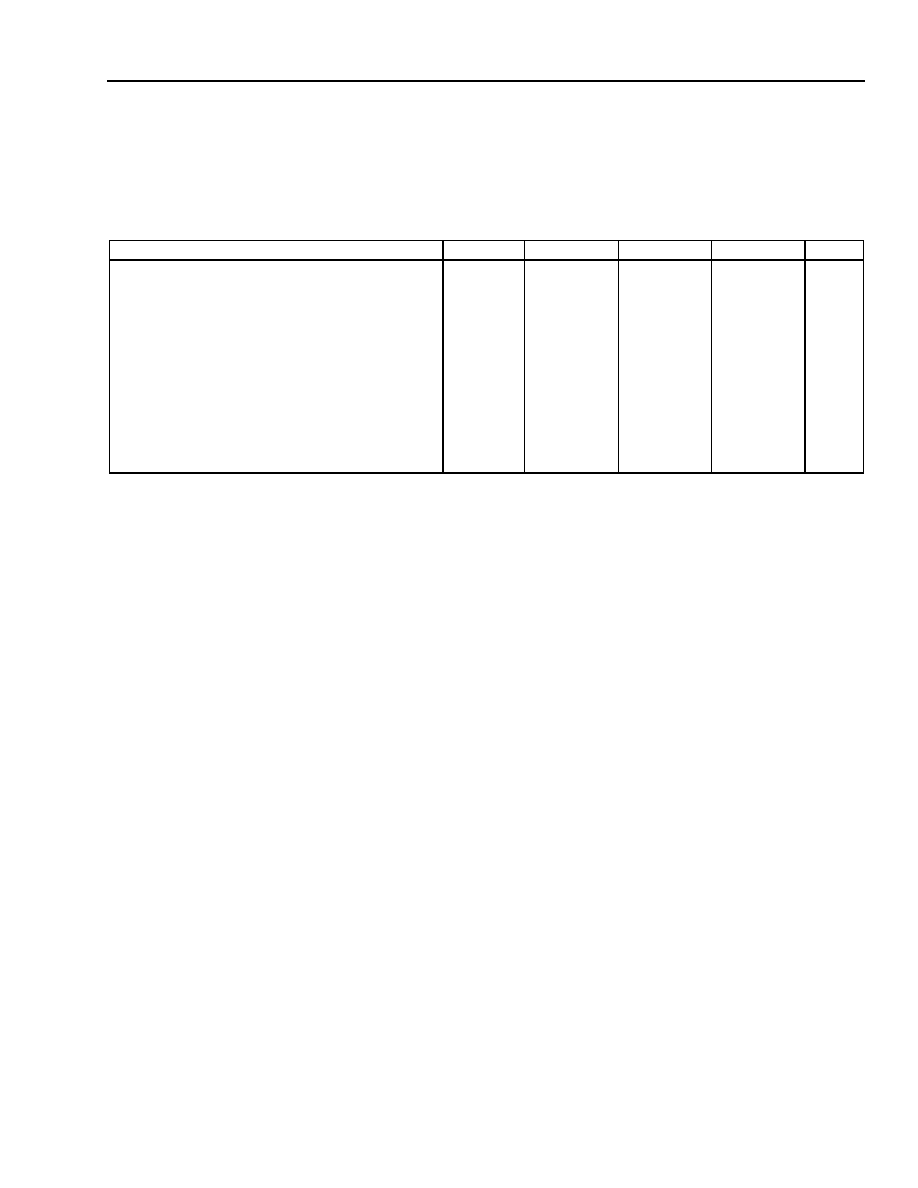
Table 1. Enable Truth Table
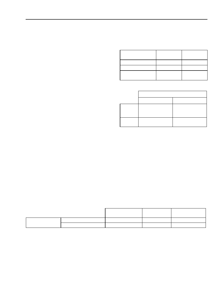
Absolute Maximum Ratings
Stresses in excess of the absolute maximum ratings can cause permanent damage to the device. These are abso-
lute stress ratings only. Functional operation of the device is not implied at these or any other conditions in excess
of those given in the operational sections of the data sheet. Exposure to absolute maximum ratings for extended
periods can adversely affect device reliability.
E1
E2
Condition
0
0
Active
1
0
Active
0
1
Disabled
1
1
Active
Parameter
Symbol
Min
Max
Unit
Power Supply Voltage
V
CC
--
6.5
V
Ambient Operating Temperature
T
A
-
40
125
∞C
Storage Temperature
T
stg
-
55
150
∞C
Agere Systems Inc.
3
Data Sheet
January 1999
BDG1A, BDP1A, BDGLA, BPNGA, BPNPA, and BPPGA
Quad Differential Drivers
Electrical Characteristics
For electrical characteristics over the entire temperature range, see Figures 7 through 9.
Table 2. Power Supply Current Characteristics
T
A
= ≠40 ∞C to +125 ∞C, V
CC
= 5 V
±
0.5 V.
* Measured with no load (BPPGA has no load on drivers C and D).
The additional power dissipation is the result of integrating the termination resistors into the device. I
CC
is measured with a 100
resistor
across the driver outputs (BPPGA has terminating resistors on drivers A and B).
Third State
These drivers produce pseudo-ECL levels, and the third-state mode is different than the conventional TTL devices.
When a driver is placed in the third state, the bases of the output transistors are pulled low, bringing the outputs
below the active-low levels. This voltage is typically 2 V for most drivers. In the bidirectional bus application, the
driver of one device, which is in its third state, may be back driven by another driver on the bus whose voltage in
the low state is lower than the third-stated device. This could come about due to differences in the drivers' indepen-
dent power supplies. In this case, the device in the third state will control the line, thus clamping the line and reduc-
ing the signal swing. If the difference voltage between the independent power supplies and the drivers is small,
then this consideration can be ignored. In the typical case, the difference voltage can be as much as 1 V without
significantly affecting the amplitude of the driving signal.
Parameter
Symbol
Min
Typ
Max
Unit
Power Supply Current (V
CC
= 5.5 V):
All Outputs Disabled:
BDG1A*, BPNGA*
I
CC
45
65
mA
BDP1A
, BPNPA
I
CC
120
160
mA
BDGLA*
I
CC
35
55
mA
BPPGA*
I
CC
85
115
mA
All Outputs Enabled:
BDG1A*, BPNGA*
I
CC
25
40
mA
BDP1A
, BPNPA
I
CC
150
200
mA
BDGLA*
I
CC
14
20
mA
BPPGA*
I
CC
90
115
mA

4
Agere Systems Inc.
Data Sheet
January 1999
BDG1A, BDP1A, BDGLA, BPNGA, BPNPA, and BPPGA
Quad Differential Drivers
Electrical Characteristics
(continued)
Table 3. Voltage and Current Characteristics
For the variation in V
OH
and V
OL
over the temperature range, see Figures 7 and 8.
T
A
= ≠40 ∞C to +125 ∞C.*
* Values are with terminations as per Figure 4 or equivalent.
The input levels and difference voltage provide zero noise immunity and should be tested only in a static, noise-free environment.
Test must be performed one lead at a time to prevent damage to the device.
ß See Figure 1 for BPPGA terminations.
Parameter
Symbol
Min
Typ
Max
Unit
Output Voltages:
Low*
V
OL
V
OH
≠
1.4
V
OH
-
1.1
V
OH
-
0.65
V
High*:
BDG1A, BDP1A, BPNGA, BPNPA, BPPGA
V
OH
V
CC
-
1.8
V
CC
-
1
V
CC
-
0.8
V
BDGLA
V
OH
V
CC
-
2.5
V
CC
-
2
V
CC
-
1.6
V
Differential Voltage (V
OH
≠ V
OL
)
V
DIFF
0.65
1.1
1.4
V
Output Voltages (T
A
= 0 ∞C to 85 ∞C):
Low*
V
OL
V
OH
≠
1.4
V
OH
-
1.1
V
OH
-
0.8
V
High*:
BDG1A, BDP1A, BPNGA, BPNPA, BPPGA
V
OH
V
CC
-
1.5
V
CC
-
1
V
CC
-
0.8
V
BDGLA
V
OH
V
CC
-
2.5
V
CC
-
2
V
CC
-
1.6
V
Differential Voltage (V
OH
≠ V
OL
)
V
DIFF
0.8
1.1
1.4
V
Third State, I
OH
= ≠1.0 mA, V
CC
= 4.5 V:
BDG1A, BDP1A, BPNGA, BPNPA, BPPGA
V
OZ
--
V
OL
-
0.5
V
OL
-
0.2
V
BDGLA
V
OZ
--
0.2
0.5
V
Input Voltages:
Low, V
CC
= 5.5 V:
Data Input
V
IL
--
--
0.8
V
Enable Input
V
IL
--
--
0.7
V
High, V
CC
= 4.5 V
V
IH
2.0
--
--
V
Clamp, V
CC
= 4.5 V, I
I
= ≠5.0 mA
V
IK
--
--
-
1.0
V
Short-circuit Output Current, V
CC
= 5.5 V
I
OS
≠100
--
--
mA
Input Currents, V
CC
= 5.5 V:
Low, V
I
= 0.4 V
I
IL
--
--
-
400
µ
A
High, V
I
= 2.7 V
I
IH
--
--
20
µ
A
Reverse, V
I
= 5.5 V
I
IH
--
--
100
µ
A
Output Resistors:
BDP1A, BPNPA, BPPGA
ß
R
O
--
220
--

Agere Systems Inc.
5
Data Sheet
January 1999
BDG1A, BDP1A, BDGLA, BPNGA, BPNPA, and BPPGA
Quad Differential Drivers
Timing Characteristics
Table 4. Timing Characteristics (See Figures 2 and 3.)
For t
P1
and t
P2
propagation delays over the temperature range, see Figure 9.
Propagation delay test circuit connected to output (see Figure 6).
T
A
= ≠40 ∞C to +125 ∞C, V
CC
= 5 V
±
0.5 V.
* t
P1
and t
P2
are measured from the 1.5 V point of the input to the crossover point of the outputs (see Figure 2).
CL = 5 pF. Capacitor is connected from each output to ground.
Parameter
Symbol
Min
Typ
Max
Unit
Propagation Delay:
Input High to Output
t
P1
*
0.8
1.2
2.0
ns
Input Low to Output
t
P2
*
0.8
1.2
2.0
ns
Capacitive Delay
t
p
--
0.02
0.03
ns/pF
Disable Time (either E1 or E2):
High-to-high Impedance
t
PHZ
4
8
12
ns
Low-to-high Impedance
t
PLZ
4
8
12
ns
Enable Time (either E1 or E2):
High Impedance to High
t
PZH
4
8
12
ns
High Impedance to Low
t
PZL
4
8
12
ns
Output Skew, |t
P1
≠ t
P2
|
t
skew1
--
0.1
0.3
ns
|t
PHH ≠
t
PHL
|, |t
PLH
≠ t
PLL
|
t
skew2
--
0.2
0.5
ns
Difference Between Drivers
t
skew
--
--
0.3
ns
Rise Time (20%--80%)
t
tLH
--
0.7
2
ns
Fall Time (80%--20%)
t
tHL
--
0.7
2
ns

6
Agere Systems Inc.
Data Sheet
January 1999
BDG1A, BDP1A, BDGLA, BPNGA, BPNPA, and BPPGA
Quad Differential Drivers
Timing Characteristics
(continued)
12-2677F
Figure 2. Driver Propagation-Delay Timing
12-2268.dC
* E2 = 1 while E1 changes state.
E1 = 0 while E2 changes state.
Note: In the third state, both outputs (i.e., OUTPUT and OUTPUT) are 0.2 V below the low state.
Figure 3. Driver Enable and Disable Timing for a High Input
INPUT
TRANSITION
OUTPUTS
OUTPUT
OUTPUT
OUTPUT
t
tLH
t
PHL
t
tHL
t
PLH
t
PHH
t
PLL
t
P2
t
P1
20%
80%
20%
80%
2.4 V
1.5 V
0.4 V
V
OH
V
OL
V
OH
(V
OH
+ V
OL
)/2
V
OL
V
OH
(V
OH
+ V
OL
)/2
V
OL
V
OH
V
OL
E1*
OUTPUT
OUTPUT
t
PHZ
t
PZH
t
PLZ
t
PZL
3.0 V
1.3 V
0.0 V
V
OH
V
OL
+ 0.2 V
V
OL
V
OL
≠ 0.1 V
V
OL
V
OL
≠ 0.1 V
E2
3.0 V
1.3 V
0.0 V

Agere Systems Inc.
7
Data Sheet
January 1999
BDG1A, BDP1A, BDGLA, BPNGA, BPNPA, and
Quad Differential Drivers
Test Conditions
Parametric values specified under the Electrical Char-
acteristics and Timing Characteristics sections for the
data transmission driver devices are measured with the
following output load circuits.
BDG1A, BPNGA, BDGLA, BPPGA (Gates A & B)
12-2271F
BDP1A, BPNPA, BPPGA (Gates C & D)
12-2271.bC
Figure 4. Driver Test Circuit
12-2640.aF
Note: Surges can be applied simultaneously, but never in opposite
polarities.
Figure 5. Lightning-Surge Testing Configuration
(BPNGA, BPNPA, and BPPGA)
Output Characteristics
Figure 6 illustrates typical driver output characteristics.
Included are load lines for two typical termination con-
figurations.
12-2269F
A. Output Current vs. Output Voltage for Loads
Shown in C and D (BDG1A, BDP1A, BPNGA,
BPNPA, and BPPGA)
12-2818aC
B. Output Current vs. Output Voltage for Loads
Shown in C and D (BDGLA)
12-2270F
C. Y Load
12-2271F
D.
Load
Figure 6. Driver Output Current vs. Voltage
Characteristics
DO(+)
DO(≠)
200
200
100
DO
DO
100
DUT
+
≠
110
110
+
≠
+5 V
+60 V
SURGE
10
µ
s
DURATION
1 ms
REPITITION
+60 V
SURGE
10
µ
s
DURATION
1 ms
REPETITION
10
20
30
40
Y LOAD
LOAD
OUTPUT VOLTAGE (V)
OUT
P
UT
CUR
RE
NT
(
m
A
)
V
OL
V
OH
V
CC
≠ 2 V
V
CC
≠ 1 V
V
CC
10
20
30
40
V
OH
V
OL
Y LOAD
LOAD
OUTPUT VOLTAGE (V)
OUTP
UT
CU
RRE
NT (mA
)
V
CC
≠ 3 V
V
CC
≠ 2 V
V
CC
≠ 1 V
V
CC
DO
60
60
90
DO
DO(+)
DO(≠)
200
200
100

8
Agere Systems Inc.
Data Sheet
January 1999
BDG1A, BDP1A, BDGLA, BPNGA, BPNPA, and BPPGA
Quad Differential Drivers
Temperature Characteristics
12-3467F
Figure 7. V
OL
and V
OH
Extremes vs. Temperature
for 100
Load
12-3468F
Figure 8. Differential Voltage (V
OH
≠ V
OL
) vs.
Temperature for 100
Load
12-3469aF
Figure 9. Min and Max for t
P1
and t
P2
Propagation
Delays vs. Temperature
Handling Precautions
CAUTION
:
This device is susceptible to damage
as a result of electrostatic discharge.
Take proper precautions during both
handling and testing. Follow guide-
lines such as JEDEC Publication No.
108-A (Dec. 1988).
When handling and mounting line driver products,
proper precautions should be taken to avoid exposure
to electrostatic discharge (ESD). The user should
adhere to the following basic rules for ESD control:
1.
Assume that all electronic components are sensi-
tive to ESD damage.
2.
Never touch a sensitive component unless properly
grounded.
3.
Never transport, store, or handle sensitive compo-
nents except in a static-safe environment.
≠25
0
25
50
75
100
≠2.5
TEMPERATURE (∞C)
≠2.0
0
125 150
≠50
≠0.5
≠1.0
≠1.5
OUTPUT
V
O
L
T
A
G
E
REL
A
TI
VE
TO
V
CC
V
OH
MAX
V
OH
MIN
V
OL
MAX
V
OL
MIN
≠25
0
25
50
75
100
0
TEMPERATURE (∞C)
0.4
1.2
125 150
≠50
1.0
0.8
0.6
DI
FFE
RE
NT
IA
L V
O
LTA
G
E
(V
)
V
OH
≠ V
OL
TYP
V
OH
≠ V
OL
MIN
≠25
0
25
50
75
100
0.5
TEMPERATURE (∞C)
0.7
1.7
125 150
≠50
2.1
2.3
PR
OP
AG
A
T
I
O
N
D
E
LAY
(n
s)
1.5
1.3
1.1
0.9
1.9
0.3
RANGE FOR t
P1
AND t
P2
MAX
MIN
Agere Systems Inc.
9
Data Sheet
January 1999
BDG1A, BDP1A, BDGLA, BPNGA, BPNPA, and
Quad Differential Drivers
ESD Failure Models
Agere employs two models for ESD events that can
cause device damage or failure.
1.
A human-body model (HBM) that is used by most
of the industry for ESD-susceptibility testing and
protection-design evaluation. ESD voltage thresh-
olds are dependent on the critical parameters used
to define the model. A standard HBM (resistance =
1500
, capacitance = 100 pF) is widely used and,
therefore, can be used for comparison purposes.
2.
A charged-device model (CDM), which many
believe is the better simulator of electronics manu-
facturing exposure.
Tables 5 and 6 illustrate the role these two models play
in the overall prevention of ESD damage. HBM ESD
testing is intended to simulate an ESD event from a
charged person. The CDM ESD testing simulates
charging and discharging events that occur in produc-
tion equipment and processes, e.g., an integrated cir-
cuit sliding down a shipping tube.
The HBM ESD threshold voltage presented here was
obtained by using these circuit parameters.
Table 5. Typical ESD Thresholds for Data
Transmission Drivers
Table 6. ESD Damage Protection
Device
HBM
Threshold
CDM
Threshold
BDG1A, BDGLA
>
2500
>
1000
BDP1A
>
2500
>
2000
BPPGA, BPNGA,
BPNPA
>
3000
>
2000
ESD Threat Controls
Personnel
Processes
Control
Wrist straps
ESD shoes
Antistatic flooring
Static-dissipative
materials
Air ionization
Model
Human-body model
(HBM)
Charged-device
model (CDM)
Latch-Up
Latch-up evaluation has been performed on the data transmission drivers. Latch-up testing determines if power-
supply current exceeds the specified maximum due to the application of a stress to the device under test. A device
is considered susceptible to latch-up if the power supply current exceeds the maximum level and remains at that
level after the stress is removed.
Agere performs latch-up testing per an internal test method that is consistent with JEDEC Standard No. 17 (previ-
ously JC-40.2) "CMOS Latch-Up Standardized Test Procedure."
Latch-up evaluation involves three separate stresses to evaluate latch-up susceptibility levels:
1. dc current stressing of input and output pins.
2. Power supply slew rate.
3. Power supply overvoltage.
Table 7. Latch-Up Test Criteria and Test Results
Based on the results in Table 6, the data transmission drivers pass the Agere latch-up testing requirements and are
considered not susceptible to latch-up.
dc Current Stress of
I/O Pins
Power Supply
Slew Rate
Power Supply
Overvoltage
Data Transmission
Driver ICs
Minimum Criteria
150 mA
1
µs
1.75
◊
Vmax
Test Results
250 mA
100 ns
2.25
◊
Vmax
10
Agere Systems Inc.
Data Sheet
January 1999
BDG1A, BDP1A, BDGLA, BPNGA, BPNPA, and BPPGA
Quad Differential Drivers
Outline Diagrams
16-Pin DIP
Dimensions are in millimeters.
5-4410r.2 (C)
Note: The dimensions in this outline diagram are intended for informational purposes only. For detailed schematics to assist your design efforts,
please contact your Agere Sales Representative.
Package
Description
Number of
Pins
(N)
Package Dimensions
Maximum Length
(L)
Maximum Width
Without Leads
(B)
Maximum Width
Including Leads
(W)
Maximum Height
Above Board
(H)
PDIP3 (Plastic
Dual-In-Line
Package)
16
20.57
6.48
7.87
5.08
W
H
0.58 MAX
2.54 TYP
0.38 MIN
SEATING PLANE
N
1
PIN #1 IDENTIFIER ZONE
L
B

Agere Systems Inc.
11
Data Sheet
January 1999
BDG1A, BDP1A, BDGLA, BPNGA, BPNPA, and BPPGA
Quad Differential Drivers
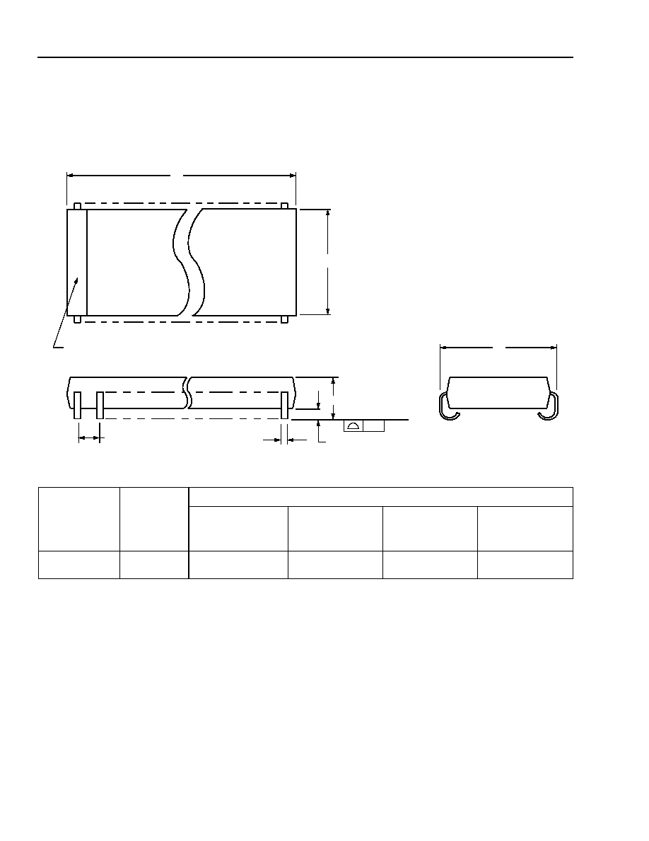
Outline Diagrams
(continued)
16-Pin SOIC (SONB/SOG)
Dimensions are in millimeters.
5-4414r.3 (C)
Note: The dimensions in this outline diagram are intended for informational purposes only. For detailed schematics to assist your design efforts,
please contact your Agere Sales Representative.
Package
Description
Number of
Pins
(N)
Package Dimensions
Maximum Length
(L)
Maximum Width
Without Leads
(B)
Maximum Width
Including Leads
(W)
Maximum Height
Above Board
(H)
SONB (Small-
Outline, Narrow
Body)
16
10.11
4.01
6.17
1.73
SOG (Small-
Outline, Gull-
Wing)
16
10.49
7.62
10.64
2.67
W
0.61
0.51 MAX
H
0.28 MAX
0.10
SEATING PLANE
1.27 TYP
N
L
B
1
PIN #1 IDENTIFIER ZONE
12
Agere Systems Inc.
Data Sheet
January 1999
BDG1A, BDP1A, BDGLA, BPNGA, BPNPA, and BPPGA
Quad Differential Drivers
Outline Diagrams
(continued)
16-Pin SOIC (SOJ)
Dimensions are in millimeters.
5-4413r.3 (C)
Note: The dimensions in this outline diagram are intended for informational purposes only. For detailed schematics to assist your design efforts,
please contact your Agere Sales Representative.
Package
Description
Number of
Pins
(N)
Package Dimensions
Maximum Length
(L)
Maximum Width
Without Leads
(B)
Maximum Width
Including Leads
(W)
Maximum Height
Above Board
(H)
SOJ (Small-
Outline, J-Lead)
16
10.41
7.62
8.81
3.18
N
1
PIN #1 IDENTIFIER ZONE
0.51 MAX
0.79 MAX
0.10
SEATING PLANE
1.27 TYP
H
W
B
L
Agere Systems Inc.
13
Data Sheet
January 1999
BDG1A, BDP1A, BDGLA, BPNGA, BPNPA, and
Quad Differential Drivers
Power Dissipation
System designers incorporating Agere data transmis-
sion drivers in their applications should be aware of
package and thermal information associated with these
components.
Proper thermal management is essential to the long-
term reliability of any plastic encapsulated integrated
circuit. Thermal management is especially important
for surface-mount devices, given the increasing circuit
pack density and resulting higher thermal density. A
key aspect of thermal management involves the junc-
tion temperature (silicon temperature) of the integrated
circuit.
Several factors contribute to the resulting junction tem-
perature of an integrated circuit:
s
Ambient use temperature
s
Device power dissipation
s
Component placement on the board
s
Thermal properties of the board
s
Thermal impedance of the package
Thermal impedance of the package is referred to as
ja
and is measured in ∞C rise in junction temperature
per watt of power dissipation. Thermal impedance is
also a function of airflow present in system application.
The following equation can be used to estimate the
junction temperature of any device:
T
j
= T
A
+
P
D
ja
where:
T
j
is device junction temperature (∞C).
T
A
is ambient temperature (∞C).
P
D
is power dissipation (W).
ja
is package thermal impedance (junction to ambi-
ent
--
∞C/W).
The power dissipation estimate is derived from two fac-
tors:
s
Internal device power
s
Power associated with output terminations
Multiplying I
CC
times V
CC
provides an estimate of inter-
nal power dissipation.
The power dissipated in the output is a function of the:
s
Termination scheme on the outputs
s
Termination resistors
s
Duty cycle of the output
Package thermal impedance depends on:
s
Airflow
s
Package type (e.g., DIP, SOIC, SOIC/NB)
The junction temperature can be calculated using the
previous equation, after power dissipation levels and
package thermal impedances are known.
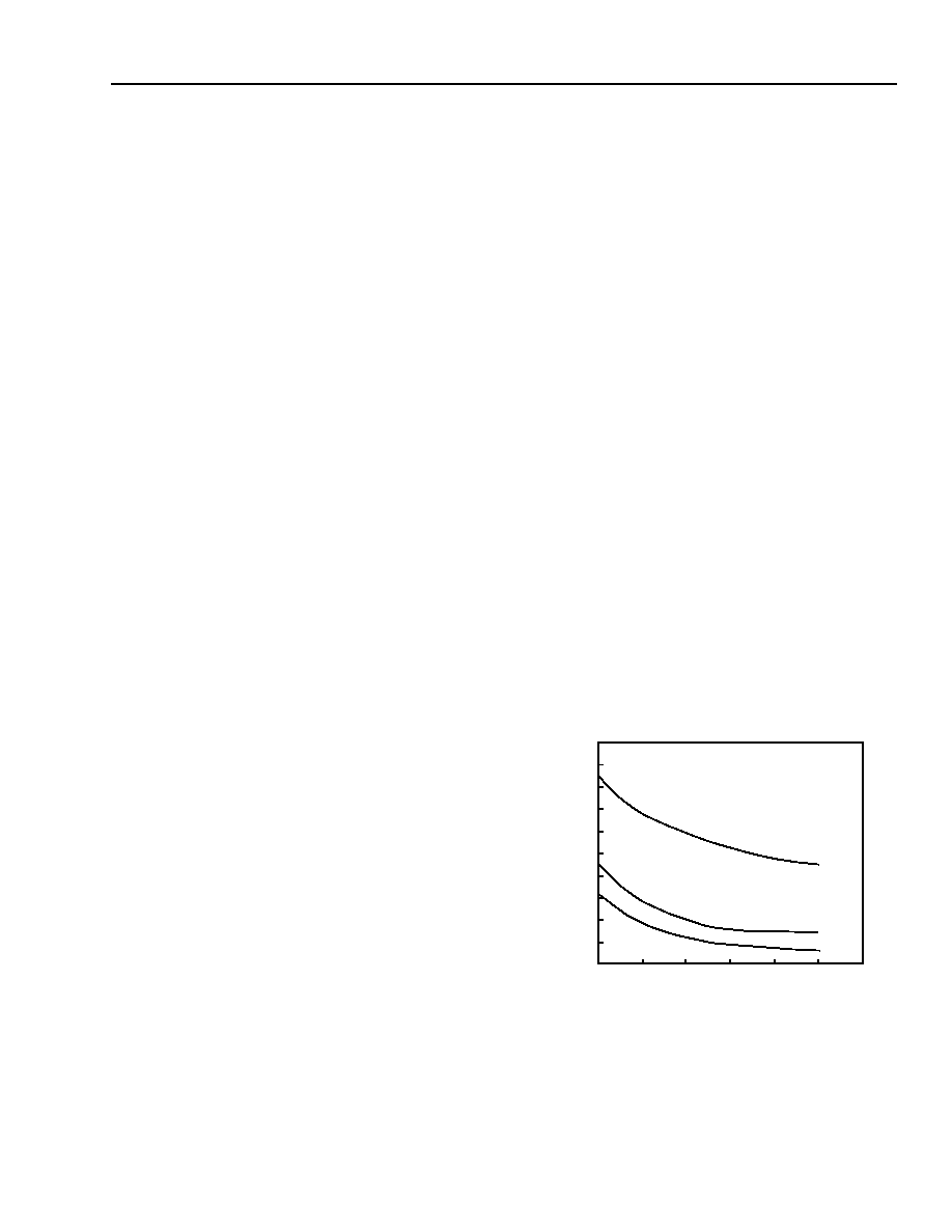
Figure 10 illustrates the thermal impedance estimates
for the various package types as a function of airflow.
This figure shows that package thermal impedance is
higher for the narrow-body SOIC package. Particular
attention should, therefore, be paid to the thermal man-
agement issues when using this package type.
In general, system designers should attempt to main-
tain junction temperature below 125 ∞C. The following
factors should be used to determine if specific data
transmission drivers in particular package types meet
the system reliability objectives:
s
System ambient temperature
s
Power dissipation
s
Package type
s
Airflow
12-2753F
Figure 10. Power Dissipation
DIP
SOIC/NB
J-LEAD SOIC/GULL WING
AIRFLOW (ft./min.)
200
400
600
800
1000
1200
0
40
50
60
70
80
90
100
110
120
130
140
T
H
ER
M
A
L R
ESI
ST
AN
C
E
ja
(
∞
C/
W
)

14
Agere Systems Inc.
Data Sheet
January 1999
BDG1A, BDP1A, BDGLA, BPNGA, BPNPA, and BPPGA
Quad Differential Drivers
Ordering Information
Part Number
Intern.
Term.
Surge
Prot.
Package Type
Comcode
Former
Pkg. Type
Former
Part #
BDG1A16E
None
No
16-pin, Plastic SOJ
107914186
1041
LG, MG, MGA
BDG1A16E-TR
None
No
Tape & Reel SOJ
107914194
1041
LG, MG, MGA
BDG1A16G
None
No
16-pin, Plastic SOIC
107914160
1141
LG, MG, MGA
BDG1A16G-TR
None
No
Tape & Reel SOIC
107914178
1141
LG, MG, MGA
BDG1A16NB
None
No
Plastic SOIC/NB
107914202
1241
LG, MG, MGA
BDG1A16NB-TR
None
No
Tape & Reel SOIC/NB
107914210
1241
LG, MG, MGA
BDG1A16P
None
No
16-pin, Plastic DIP
107914004
41
LG, MG, MGA
BDP1A16E
220
No
16-pin, Plastic SOJ
107914293
1041
LP, MP, MPA
BDP1A16E-TR
220
No
Tape & Reel SOJ
107914301
1041
LP, MP, MPA
BDP1A16G
220
No
16-pin, Plastic SOIC
107914319
1141
LP, MP, MPA
BDP1A16G-TR
220
No
Tape & Reel SOIC
107914327
1141
LP, MP, MPA
BDP1A16P
220
No
16-pin, Plastic DIP
107914335
41
LP, MP, MPA
BDGLA16E
None
No
16-pin, Plastic SOJ
107914228
1041
MGL3
BDGLA16E-TR
None
No
Tape & Reel SOJ
107914236
1041
MGL3
BDGLA16G
None
No
16-pin, Plastic SOIC
107914244
1141
MGL3
BDGLA16G-TR
None
No
Tape & Reel SOIC
107914251
1141
MGL3
BDGLA16NB
None
No
Plastic SOIC/NB
107914269
1241
MGL3
BDGLA16NB-TR
None
No
Tape & Reel SOIC/NB
107914277
1241
MGL3
BDGLA16P
None
No
16-pin, Plastic DIP
107914285
41
MGL3
BPNGA16E
None
Yes
16-pin, Plastic SOJ
107914343
1041
NG
BPNGA16E-TR
None
Yes
Tape & Reel SOJ
107914350
1041
NG
BPNGA16G
None
Yes
16-pin, Plastic SOIC
107914368
1141
NG
BPNGA16G-TR
None
Yes
Tape & Reel SOIC
107914376
1141
NG
BPNGA16NB
None
Yes
Plastic SOIC/NB
107914384
1241
NG
BPNGA16NB-TR
None
Yes
Tape & Reel SOIC/NB
107914392
1241
NG
BPNGA16P
None
Yes
16-pin, Plastic DIP
107914400
41
NG
BPNPA16E
220
Yes
16-pin, Plastic SOJ
107914418
1041
NP
BPNPA16E-TR
220
Yes
Tape & Reel SOJ
107914426
1041
NP
BPNPA16G
220
Yes
16-pin, Plastic SOIC
107914434
1141
NP
BPNPA16G-TR
220
Yes
Tape & Reel SOIC
107914442
1141
NP
BPNPA16P
220
Yes
16-pin, Plastic DIP
107949745
41
NP
BPPGA16E
220
Yes
16-pin, Plastic SOJ
107949752
1041
PG
BPPGA16E-TR
220
Yes
Tape & Reel SOJ
107949760
1041
PG
BPPGA16G
220
Yes
16-pin, Plastic SOIC
107949778
1141
PG
BPPGA16G-TR
220
Yes
Tape & Reel SOIC
107949786
1141
PG
BPPGA16P
220
Yes
16-pin, Plastic DIP
107949794
41
PG

Agere Systems Inc.
15
Data Sheet
January 1999
BDG1A, BDP1A, BDGLA, BPNGA, BPNPA, and BPPGA
Quad Differential Drivers
Notes

Copyright © 2002 Agere Systems Inc.
All Rights Reserved
January 1999
DS99-144HSI (Replaces DS99-044HSI)
Agere Systems Inc. reserves the right to make changes to the product(s) or information contained herein without notice. No liability is assumed as a result of their use or application.
For additional information, contact your Agere Systems Account Manager or the following:
INTERNET:
http://www.agere.com
E-MAIL:
docmaster@agere.com
N. AMERICA:
Agere Systems Inc., 555 Union Boulevard, Room 30L-15P-BA, Allentown, PA 18109-3286
1-800-372-2447, FAX 610-712-4106 (In CANADA: 1-800-553-2448, FAX 610-712-4106)
ASIA:
Agere Systems Hong Kong Ltd., Suites 3201 & 3210-12, 32/F, Tower 2, The Gateway, Harbour City, Kowloon
Tel. (852) 3129-2000, FAX (852) 3129-2020
CHINA: (86) 21-5047-1212 (Shanghai), (86) 10-6522-5566 (Beijing), (86) 755-695-7224 (Shenzhen)
JAPAN: (81) 3-5421-1600 (Tokyo), KOREA: (82) 2-767-1850 (Seoul), SINGAPORE: (65) 778-8833, TAIWAN: (886) 2-2725-5858 (Taipei)
EUROPE:
Tel. (44) 7000 624624, FAX (44) 1344 488 045