 | –≠–ª–µ–∫—Ç—Ä–æ–Ω–Ω—ã–π –∫–æ–º–ø–æ–Ω–µ–Ω—Ç: CA16A2Cnn | –°–∫–∞—á–∞—Ç—å:  PDF PDF  ZIP ZIP |
CA16-Type 2.5 Gbits/s DWDM Transponder with
16-Channel 155 Mbits/s Multiplexer/Demultiplexer
Advance Data Sheet
March 2001
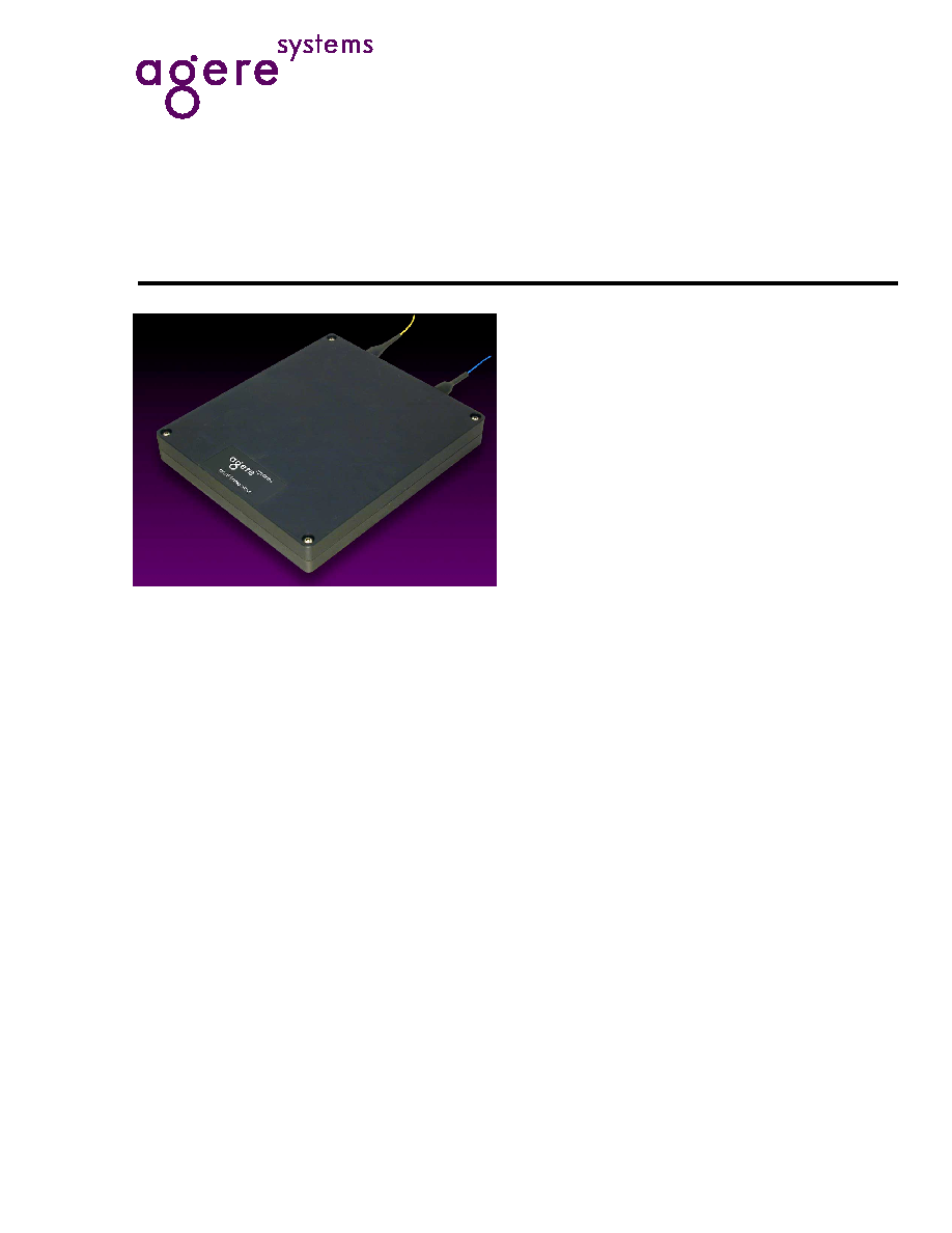
The CA16-type
transponders integrate up to 15 discrete
ICs and optical components, including a 2.5Gbits/s op-
tical transmitter and receiver pair, all in a single, com-
pact package.
Features
s
2.5 Gbits/s optical transmitter and receiver with
16-channel 155 Mbits/s multiplexer/demultiplexer.
s
Available with 1.55 µm cooled DFB laser transmit-
ter and an APD receiver for long-reach applica-
tions:
-- Offers 45 standard ITU wavelengths with
100 GHz spacing.
-- Each module is capable of two wavelengths
under user control.
s
Pigtailed, low-profile package.
s
Differential LVPECL data interface.
s
Operating case temperature range: 0 ∞C to 65 ∞C.
s
Automatic transmitter optical power control.
s
Laser bias monitor output.
s
Transmitter laser disable input.
s
Line loopback and diagnostic loopback capability.
s
Multiple alarms:
-- Loss of signal.
-- Loss of reference clock.
-- Loss of framing.
-- Laser degrade alarm.
Applications
s
Telecommunications:
-- Inter- and intraoffice SONET/SDH
-- Subscriber loop
-- Metropolitan area networks
s
High-speed data communications
Description
The CA16-type transponder performs the parallel-to-
serial-to-optical transport and optical transport-to-
serial-to-parallel function of the section and photonic
layers of the SONET/SDH protocol. The CA16 trans-
mitter section performs the bit serialization and opti-
cal transmission of SONET/SDH OC-48/STM-16
data that has been formatted into standard SONET/
SDH compliant 16-bit parallel format. The CA16
receiver performs the optical-to-electrical conversion
function and is then able to detect frame and byte
boundaries and demultiplex the serial data into 16-bit
parallel OC-48/STM-16 format.
The CA16 transponder does not perform byte-level
multiplexing or interleaving.

2
Table of Contents
Agere Systems Inc..
Contents
Page
Tables
Page
CA16-Type 2.5 Gbits/s DWDM Transponder with
Advance Data Sheet
16-Channel 155 Mbits/s Multiplexer/Demultiplexer
March 2001
Features ................................................................... 1
Applications .............................................................. 1
Description ............................................................... 1
Absolute Maximum Ratings ...................................... 3
Block Diagram........................................................... 4
Pin Information ......................................................... 5
Pin Descriptions ....................................................... 6
Functional Description ........................................... 12
Receiver ............................................................ 12
Transmitter ........................................................ 12
Loopback Modes ............................................... 13
Transponder Interfacing ..................................... 13
Optical Characteristics ........................................... 15
Electrical Characteristics ........................................ 16
Timing Characteristics ........................................... 18
Transmitter Data Input Timing ........................... 18
Input Timing Mode 1 .......................................... 19
Input Timing Mode 2 .......................................... 20
Forward Clocking ............................................... 21
PC
LK
-to PIC
LK
Timing ........................................ 22
PHERR/PHINIT .................................................. 23
Receiver Framing ............................................... 25
Wavelength Selection ............................................. 26
Qualification and Reliability .................................... 27
Laser Safety Information ....................................... 27
Class I Laser Product ......................................... 27
Electromagnetic Emissions and Immunity.......... 27
Outline Diagram ..................................................... 28
Ordering Information .............................................. 29
Related Product Information ................................... 29
Table 1. CA16-Type Transponder Pinout ................. 6
Table 2. CA16-Type Transponder Input Pin
Descriptions ............................................... 10
Table 3. CA16-Type Transponder Output Pin
Descriptions ............................................... 11
Table 4. OC-48/STM-16 Transmitter Optical
Characteristics .......................................... 15
Table 5. OC-48/STM-16 Receiver Optical
Characteristics .......................................... 15
Table 6. Power Supply Characteristics .................... 16
Table 7. Transmitter Electrical I/O Characteristics ... 16
Table 8. Receiver Electrical I/O Characteristics ...... 17
Table 9. Transmitter ac Timing Characteristics ....... 24
Table 10. Receiver ac Timing Characteristics ......... 24
Table 11. Ordering Information ................................ 29
Table 12. Related Product Information .................... 29
Figures
Page
Figure 1. CA16-Type Transponder Block Diagram.... 4
Figure 2. CA16-Type Transponder Pinout ................. 5
Figure 3. Transponder Interfacing............................ 13
Figure 4. Interfacing to the T
X
R
EF
C
LK
Input............. 14
Figure 5. Block Diagram Timing Mode 1.................. 19
Figure 6. Block Diagram Timing Mode 2.................. 20
Figure 7. Forward Clocking of the
CA16 Transponder .................................. 21
Figure 8. PC
LK
-to PIC
LK
Timing ...............................22
Figure 9. PHERR/PHINIT Timing............................. 23
Figure 10. ac Input Timing ....................................... 24
Figure 11. Receiver Output Timing Diagram ........... 24
Figure 12. Frame and Byte Detection ...................... 25
Figure 13. OOF Timing (FRAMEN = High) .............. 25
Figure 14. FRAMEN Timing ..................................... 26

3
Agere Systems Inc.
Advance Data Sheet
CA16-Type 2.5 Gbits/s DWDM Transponder with
March 2001
16-Channel 155 Mbits/s Multiplexer/Demultiplexer
Description
(continued)
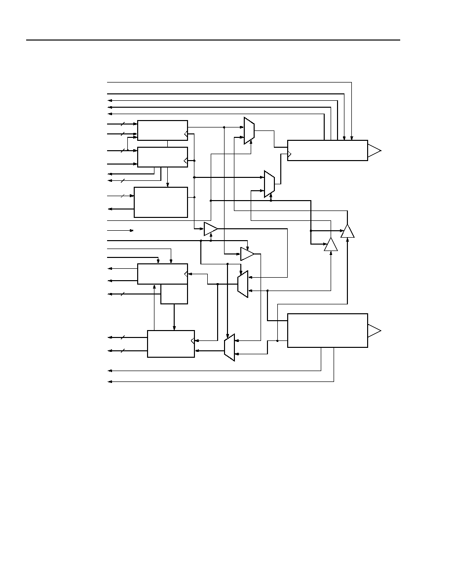
Figure 1 shows a simplified block diagram of the CA16-
Type transponder. This device is a bidirectional module
designed to provide a SONET or SDH compliant elec-
tro-optical interface between the SONET/SDH photonic
physical layer and the electrical section layer. The mod-
ule contains a wavelength-tunable (two channels at
100 GHz) 2.5 Gbits/s optical transmitter and a
2.5 Gbits/s optical receiver in the same physical pack-
age along with the electronics necessary to multiplex
and demultiplex sixteen 155 Mbits/s electrical channels.
Clock synthesis, clock recovery, and SONET/SDH
frame detection circuits are also included within the
module.
In the transmit direction, the transponder module multi-
plexes sixteen 155 Mbits/s PECL electrical data signals
into an optical signal at 2488.32 Mbits/s for launching
into optical fiber. An internal 2.488 GHz reference oscil-
lator is phase-locked to an external 155.52 MHz data
timing reference.
The optical transmitter is available at any ITU grid
wavelength with a 1.55 µm cooled DFB laser for long-
reach applications. The optical output signal is SONET
and ITU compliant for OC-48/STM-16 applications as
shown in Table 4, OC-48/STM-16 Transmitter Optical
Characteristics.
In the receive direction, the transponder module
receives a 2488.32 Mbits/s optical signal and converts
it to an electrical signal, and then extracts a clock sig-
nal and demultiplexes the data into sixteen 155 Mbits/s
differential LVPECL data signals. When enabled, the
module can also detect SONET/SDH frame bound-
aries. The optical receiver is available with an APD
photodetector. The receiver operates over the wave-
length range of 1.1 µm to 1.6 µm and is fully compliant
to SONET/SDH OC-48/STM-16 physical layer specifi-
cations as shown in Table 5, OC-48/STM-16 Receiver
Optical Characteristics.
Absolute Maximum Ratings
Stresses in excess of the absolute maximum ratings can cause permanent damage to the device. These are abso-
lute stress ratings only. Functional operation of the device is not implied at these or any other conditions in excess
of those given in the operations sections of the data sheet. Exposure to absolute maximum ratings for extended
periods can adversely affect reliability.
1. Human body model.
Parameter
Symbol
Min
Max
Unit
Operating Case Temperature Range
T
C
0
75
∞C
Storage Case Temperature Range
T
S
≠40
85
∞C
Supply Voltage
--
≠0.5
5.5
V
Voltage on Any LVPECL Pin
--
0
V
CC
--
High-speed LVPECL Output Source Current
--
--
50
mA
Static Discharge Voltage
1
ESD
--
500
V
Relative Humidity (noncondensing)
RH
--
85
%
Receiver Optical Input Power--Biased APD
P
IN
--
0
dBm
Minimum Fiber Bend Radius
--
1.25 (31.8)
--
in. (mm)
4
Agere Systems Inc.
CA16-Type 2.5 Gbits/s DWDM Transponder with
Advance Data Sheet
16-Channel 155 Mbits/s Multiplexer/Demultiplexer
March 2001
Block Diagram
Figure 1. CA16-Type Transponder Block Diagram
OC-48/STM-16
OPTICAL TRANSMITTER
D
CK
D
OC-48/STM-16
OPTICAL RECEIVER
W/CLOCK RECOVERY
16:1 PARALLEL
TIMING
CLOCK DIVIDER
FRAME/BYTE
TIMING
1:16 SERIAL
MU
X
MU
X
TXDIS
MU
X
GENERATION
TO SERIAL
AND
PHASE DETECT
DETECT
GEN
TO PARALLEL
MU
X
WDEA
LSR ALRM
LPM
TXD[0:15]P
TXD[0:15]N
PICLKP/N
PHINIT
PHERR
PCLKP/N
TXREFCLKP/N
LLOOP
DLOOP
OOF
SEARCH
FP
POCLKP/N
RXQ[0:15]P
RXQ[0:15]N
LOS
16
16
2
2
2
2
16
16
FRAMEN
WS (WAVELENGTH
SELECT)
LOCKDET
RESET
IPDMON
1-1011(F).f
5
Agere Systems Inc.
Advance Data Sheet
CA16-Type 2.5 Gbits/s DWDM Transponder with
March 2001
16-Channel 155 Mbits/s Multiplexer/Demultiplexer
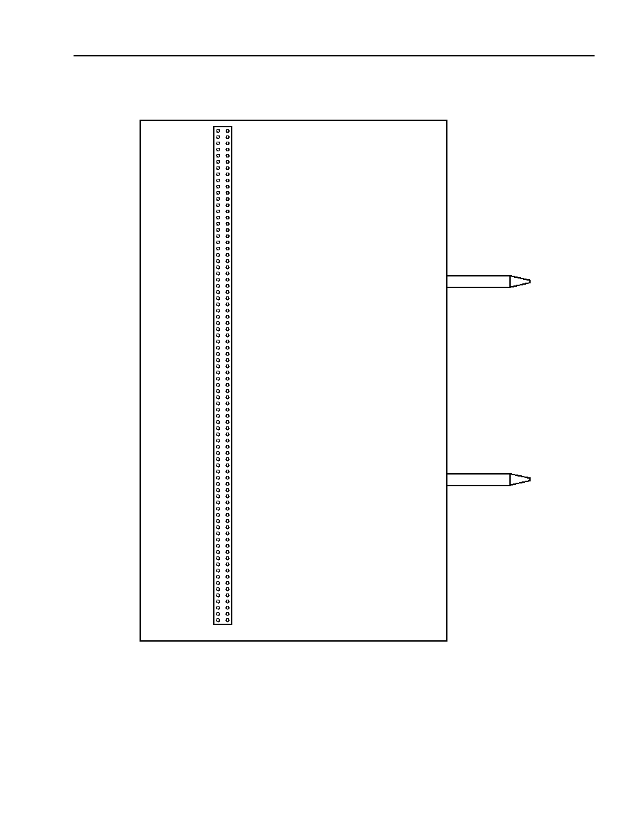
Pin Information
1-1014(F).d
Figure 2. CA16-Type Transponder Pinout
RXQ13N
RXQ13P
RXQ15N
RXQ15P
RXDGND
VTEC
VTEC
WS
NC
POCLKN
POCLKP
RX3.3A
RXAGND
RXAGND
SEARCH
RX3.3D
RX3.3D
RXDGND
OOF
RXDGND
LOS
LLOOP
PHERR
NC
TXDIS
PHINIT
NC
TX3.3A
TX3.3D
TXAGND
TXDGND
PCLKN
PCLKP
TXDGND
TXD00N
TXD00P
TXDGND
TXD02N
TXD02P
TXD04N
TXD04P
TXDGND
TXD06N
TXD06P
TXD08N
TXD08P
TXDGND
TXD10N
TXD10P
TXD12N
TXD12P
TXDGND
TXD14N
TXD14P
TXREFCLKN
TXDGND
RESET
FGND
RXDGND
RXQ12N
RXQ12P
RXQ14N
RXQ14P
RXDGND
VTEC
VTEC
VTEC
RXDGND
RXAGND
RXAGND
RX3.3A
RXAGND
RXAGND
NC
RX3.3D
FP
WDEA
DLOOP
NC
LSRBIAS
LSRALM
LPM
TXAGND
TX3.3A
TX3.3A
TXAGND
TX3.3D
TX3.3D
TXDGND
LOCKDET
PICLKN
PICLKP
TXDGND
TXD01N
TXD01P
TXD03N
TXD03P
TXDGND
TXD05N
TXD05P
TXD07P
TXDGND
TXD09N
TXD09P
TXD11N
TXD11P
TXDGND
TXD13N
TXD13P
TXD15N
TXD15P
TXDGND
IPDMON
FGND
RXDGND
140
60
130
50
120
40
110
30
100
20
90
10
1
81
TX
TXREFCLKP
TXD07N
FRAMEN
RX3.3D
RXDGND
RXQ05N
RXQ05P
RXQ07N
RXQ07P
RXDGND
RXQ09N
RXQ09P
RXQ11N
RXQ11P
RXDGND
RXQ04N
RXQ04P
RXQ06N
RXQ06P
RXDGND
RXQ08N
RXQ08P
RXQ10N
RXQ10P
RXDGND
150
70
NC
NC
NC
NC
RXDGND
RXQ01N
RXQ01P
RXQ03N
RXQ03P
FGND
NC
NC
NC
NC
RXDGND
RXQ00N
RXQ00P
RXQ02N
RXQ02P
FGND
160
80
RX
TOP VIEW

6
Agere Systems Inc.
CA16-Type 2.5 Gbits/s DWDM Transponder with
Advance Data Sheet
16-Channel 155 Mbits/s Multiplexer/Demultiplexer
March 2001
Pin Descriptions
Table 1. CA16-Type Transponder Pinout
Pin #
Pin Name
I/O
Logic
Description
01
FGND
I
Supply
Frame Ground
1
02
IPDMON
O
Analog
Receiver Photodiode Current Monitor
03
TxDGND
I
Supply
Transmitter Digital Ground
04
TxD15P
I
LVPECL
Transmitter 155 Mbits/s MSB Data Input
05
TxD15N
I
LVPECL
Transmitter 155 Mbits/s MSB Data Input
06
TxD13P
I
LVPECL
Transmitter 155 Mbits/s Data Input
07
TxD13N
I
LVPECL
Transmitter 155 Mbits/s Data Input
08
TxDGND
I
Supply
Transmitter Digital Ground
09
TxD11P
I
LVPECL
Transmitter 155 Mbits/s Data Input
10
TxD11N
I
LVPECL
Transmitter 155 Mbits/s Data Input
11
TxD09P
I
LVPECL
Transmitter 155 Mbits/s Data Input
12
TxD09N
I
LVPECL
Transmitter 155 Mbits/s Data Input
13
TxDGND
I
SUPPLY
Transmitter Digital Ground
14
TxD07P
I
LVPECL
Transmitter 155 Mbits/s Data Input
15
TxD07N
I
LVPECL
Transmitter 155 Mbits/s Data Input
16
TxD05P
I
LVPECL
Transmitter 155 Mbits/s Data Input
17
TxD05N
I
LVPECL
Transmitter 155 Mbits/s Data Input
18
TxDGND
I
Supply
Transmitter Digital Ground
19
TxD03P
I
LVPECL
Transmitter 155 Mbits/s Data Input
20
TxD03N
I
LVPECL
Transmitter 155 Mbits/s Data Input
21
TxD01P
I
LVPECL
Transmitter 155 Mbits/s Data Input
22
TxD01N
I
LVPECL
Transmitter 155 Mbits/s Data Input
23
TxDGND
I
Supply
Transmitter Digital Ground
24
PIC
LK
P
I
LVPECL
Byte-Aligned Parallel Input Clock at 155 MHz
25
PIC
LK
N
I
LVPECL
Byte-Aligned Parallel Input Clock at 155 MHz
26
LOCKDET
O
LVTTL
Lock Detect
27
TxDGND
I
Supply
Transmitter Digital Ground
28
Tx3.3D
I
Supply
Transmitter 3.3 V Digital Supply
29
Tx3.3D
I
Supply
Transmitter 3.3 V Digital Supply
30
TxAGND
I
Supply
Transmitter Analog Ground
31
Tx3.3A
I
Supply
Transmitter 3.3 V Analog Supply
32
Tx3.3A
I
Supply
Transmitter 3.3 V Analog Supply
33
TxAGND
I
Supply
Transmitter Analog Ground
34
LPM
O
Analog
Laser Power Monitor
35
LSRALM
O
5 V CMOS Laser Degrade Alarm
36
LSRBIAS
O
Analog
Not Implemented on the CA16-Type Transponder
37
NC
--
--
No User Connection Permitted
2
38
D
LOOP
I
LVTTL
Diagnostic Loopback
39
WDEA
O
5 V CMOS Wavelength Deviation Error Alarm
40
FP
O
LVPECL
Frame Pulse
41
FRAMEN
I
LVTTL
Frame Enable
1. Frame ground is connected to the housing and is isolated from all circuit grounds (TxDGND, TxAGND, RxDGND, RxAGND).
2. Pins labeled no connection must remain open circuits; they have internal voltages and must not be connected to V
CC
, Ground,
or any signal node.

7
Agere Systems Inc.
Advance Data Sheet
CA16-Type 2.5 Gbits/s DWDM Transponder with
March 2001
16-Channel 155 Mbits/s Multiplexer/Demultiplexer
42
RxDGND
I
Supply
Receiver Digital Ground
43
Rx3.3D
I
Supply
Receiver 3.3 V Digital Supply
44
Rx3.3D
I
Supply
Receiver 3.3 V Digital Supply
45
NC
--
--
No User Connection Permitted
2
46
RxAGND
I
Supply
Receiver Analog Ground
47
RxAGND
I
Supply
Receiver Analog Ground
48
Rx3.3A
I
Supply
Receiver 3.3 V Analog Supply
49
RxAGND
I
Supply
Receiver Analog Ground
50
RxAGND
I
Supply
Receiver Analog Ground
51
RxDGND
I
Supply
Receiver Digital Ground
52
VTEC
I
Supply
TEC Cooler 3 V Analog Supply Voltage
53
VTEC
I
Supply
TEC Cooler 3 V Analog Supply Voltage
54
VTEC
I
Supply
TEC Cooler 3 V Analog Supply Voltage
55
RxDGND
I
Supply
Receiver Digital Ground
56
RxQ14P
O
LVPECL
Receiver 155 Mbits/s Data Output
57
RxQ14N
O
LVPECL
Receiver 155 Mbits/s Data Output
58
RxQ12P
O
LVPECL
Receiver 155 Mbits/s Data Output
59
RxQ12N
O
LVPECL
Receiver 155 Mbits/s Data Output
60
RxDGND
I
Supply
Receiver Digital Ground
61
RxQ10P
O
LVPECL
Receiver 155 Mbits/s Data Output
62
RxQ10N
O
LVPECL
Receiver 155 Mbits/s Data Output
63
RxQ08P
O
LVPECL
Receiver 155 Mbits/s Data Output
64
RxQ08N
O
LVPECL
Receiver 155 Mbits/s Data Output
65
RxDGND
I
SUPPLY
Receiver Digital Ground
66
RxQ06P
O
LVPECL
Receiver 155 Mbits/s Data Output
67
RxQ06N
O
LVPECL
Receiver 155 Mbits/s Data Output
68
RxQ04P
O
LVPECL
Receiver 155 Mbits/s Data Output
69
RxQ04N
O
LVPECL
Receiver 155 Mbits/s Data Output
70
RxDGND
I
Supply
Receiver Digital Ground
71
RxQ02P
O
LVPECL
Receiver 155 Mbits/s Data Output
72
RxQ02N
O
LVPECL
Receiver 155 Mbits/s Data Output
73
RxQ00P
O
LVPECL
Receiver 155 Mbits/s LSB Data Output
74
RxQ00N
O
LVPECL
Receiver 155 Mbits/s LSB Data Output
75
RxDGND
I
Supply
Receiver Digital Ground
76
NC
--
--
No User Connection Permitted
2
77
NC
--
--
No User Connection Permitted
2
78
NC
--
--
No User Connection Permitted
2
79
NC
--
--
No User Connection Permitted
2
80
FGND
I
Supply
Frame Ground
1
81
FGND
I
Supply
Frame Ground
1
82
Reset
I
--
Master Reset
Pin #
Pin Name
I/O
Logic
Description
Pin Descriptions
(continued)
Table 1. CA16-Type Transponder Pinout (continued)
1. Frame ground is connected to the housing and is isolated from all circuit grounds (TxDGND, TxAGND, RxDGND, RxAGND).
2. Pins labeled no connection must remain open circuits; they have internal voltages and must not be connected to V
CC
, Ground,
or any signal node.

8
Agere Systems Inc.
CA16-Type 2.5 Gbits/s DWDM Transponder with
Advance Data Sheet
16-Channel 155 Mbits/s Multiplexer/Demultiplexer
March 2001
83
TxDGND
I
Supply
Transmitter Digital Ground
84
TxR
EF
C
LK
P
I
LVPECL
Transmitter 155 Mbits/s Reference Clock Input
85
TxR
EF
C
LK
N
I
LVPECL
Transmitter 155 Mbits/s Reference Clock Input
86
TxD14P
I
LVPECL
Transmitter 155 Mbits/s Data Input
87
TxD14N
I
LVPECL
Transmitter 155 Mbits/s Data Input
88
TxDGND
I
Supply
Transmitter Digital Ground
89
TxD12P
I
LVPECL
Transmitter 155 Mbits/s Data Input
90
TxD12N
I
LVPECL
Transmitter 155 Mbits/s Data Input
91
TxD10P
I
LVPECL
Transmitter 155 Mbits/s Data Input
92
TxD10N
I
LVPECL
Transmitter 155 Mbits/s Data Input
93
TxDGND
I
SUPPLY
Transmitter Digital Ground
94
TxD08P
I
LVPECL
Transmitter 155 Mbits/s Data Input
95
TxD08N
I
LVPECL
Transmitter 155 Mbits/s Data Input
96
TxD06P
I
LVPECL
Transmitter 155 Mbits/s Data Input
97
TxD06N
I
LVPECL
Transmitter 155 Mbits/s Data Input
98
TxDGND
I
Supply
Transmitter Digital Ground
99
TxD04P
I
LVPECL
Transmitter 155 Mbits/s Data Input
100
TxD04N
I
LVPECL
Transmitter 155 Mbits/s Data Input
101
TxD02P
I
LVPECL
Transmitter 155 Mbits/s Data Input
102
TxD02N
I
LVPECL
Transmitter 155 Mbits/s Data Input
103
TxDGND
I
SUPPLY
Transmitter Digital Ground
104
TxD00P
I
LVPECL
Transmitter 155 Mbits/s LSB Data Input
105
TxD00N
I
LVPECL
Transmitter 155 Mbits/s LSB Data Input
106
TxDGND
I
Supply
Transmitter Digital Ground
107
PC
LK
P
O
LVPECL
Transmitter Parallel Reference Clock Output
108
PC
LK
N
I
LVPECL
Transmitter Parallel Reference Clock Output
109
TxDGND
I
Supply
Transmitter Digital Ground
110
TxAGND
I
Supply
Transmitter Analog Ground
111
Tx3.3D
I
Supply
Transmitter Digital 3.3 V Supply
112
Tx3.3A
I
Supply
Transmitter Analog 3.3 V Supply
113
NC
--
--
Future Function (I
2
C Clock)
114
PHINIT
I
LVPECL
Phase Initialization
115
T
X
DIS
I
TTL
Transmitter Disable
116
NC
--
--
Future Function (I
2
C Data)
117
PHERR
O
LVPECL
Phase Error
118
L
LOOP
I
LVTTL
Line Loopback (active-low)
119
LOS
O
LVTTL
Loss of Signal
120
RxDGND
I
Supply
Receiver Digital Ground
121
OOF
I
LVTTL
Out of Frame (enable frame detection)
122
RxDGND
I
Supply
Receiver Digital Ground
123
Rx3.3D
I
Supply
Receiver Digital 3.3 V Supply
Pin #
Pin Name
I/O
Logic
Description
Pin Descriptions
(continued)
Table 1. CA16-Type Transponder Pinout (continued)
1. Frame ground is connected to the housing and is isolated from all circuit grounds (TxDGND, TxAGND, RxDGND, RxAGND).
2. Pins labeled no connection must remain open circuits; they have internal voltages and must not be connected to V
CC
, Ground,
or any signal node.

9
Agere Systems Inc.
Advance Data Sheet
CA16-Type 2.5 Gbits/s DWDM Transponder with
March 2001
16-Channel 155 Mbits/s Multiplexer/Demultiplexer
1. Frame ground is connected to the housing and is isolated from all circuit grounds (TxDGND, TxAGND, RxDGND, RxAGND).
2. Pins labeled no connection must remain open circuits; they have internal voltages and must not be connected to V
CC
, Ground, or any signal
node.
124
Rx3.3D
I
SUPPLY
Receiver Digital 3.3 V Supply
125
SEARCH
O
LVTTL
Frame Search Output
126
RxAGND
I
Supply
Receiver Analog Ground
127
RxAGND
I
Supply
Receiver Analog Ground
128
Rx3.3A
I
Supply
Receiver Analog 3.3 V Supply
129
POC
LK
P
O
LVPECL
Byte-Aligned Parallel Output Clock at 155 MHz
130
POC
LK
N
O
LVPECL
Byte-Aligned Parallel Output Clock at 155 MHz
131
NC
--
--
No User Connection Permitted
2
132
WS
I
LVTTL
Binary Input to Select One of Two Grid Wavelengths
133
VTEC
I
Supply
TEC Cooler 3 V Analog Supply Voltage
134
VTEC
I
Supply
TEC Cooler 3 V Analog Supply Voltage
135
RxDGND
I
Supply
Receiver Digital Ground
136
RxQ15P
O
LVPECL
Receiver MSB 155 Mbits/s Data Output
137
RxQ15N
O
LVPECL
Receiver MSB 155 Mbits/s Data Output
138
RxQ13P
O
LVPECL
Receiver 155 Mbits/s Data Output
139
RxQ13N
O
LVPECL
Receiver 155 Mbits/s Data Output
140
RxDGND
I
Supply
Receiver Digital Ground
141
RxQ11P
O
LVPECL
Receiver 155 Mbits/s Data Output
142
RxQ11N
O
LVPECL
Receiver 155 Mbits/s Data Output
143
RxQ09P
O
LVPECL
Receiver 155 Mbits/s Data Output
144
RxQ09N
O
LVPECL
Receiver 155 Mbits/s Data Output
145
RxDGND
I
Supply
Receiver Digital Ground
146
RxQ07P
O
LVPECL
Receiver 155 Mbits/s Data Output
147
RxQ07N
O
LVPECL
Receiver 155 Mbits/s Data Output
148
RxQ05P
O
LVPECL
Receiver 155 Mbits/s Data Output
149
RxQ05N
O
LVPECL
Receiver 155 Mbits/s Data Output
150
RxDGND
I
Supply
Receiver Digital Ground
151
RxQ03P
O
LVPECL
Receiver 155 Mbits/s Data Output
152
RxQ03N
O
LVPECL
Receiver 155 Mbits/s Data Output
153
RxQ01P
O
LVPECL
Receiver 155 Mbits/s Data Output
154
RxQ01N
O
LVPECL
Receiver 155 Mbits/s Data Output
155
RxDGND
I
Supply
Receiver Digital Ground
156
NC
--
--
No User Connection Permitted
2
157
NC
--
--
No User Connection Permitted
2
158
NC
--
--
No User Connection Permitted
2
159
NC
--
--
No User Connection Permitted
2
160
FGND
I
Supply
Frame Ground
1
Pin #
Pin Name
I/O
Logic
Description
Pin Descriptions
(continued)
Table 1. CA16-Type Transponder Pinout (continued)

10
Agere Systems Inc.
CA16-Type 2.5 Gbits/s DWDM Transponder with
Advance Data Sheet
16-Channel 155 Mbits/s Multiplexer/Demultiplexer
March 2001
Pin Descriptions
(continued)
* Future versions of the cooled transponder will not support the frame-detect function.
Table 2. CA16-Type Transponder Input Pin Descriptions
Pin Name
Pin Description
TxD[0:15]P
TxD[0:15]N
16-Bit Differential LVPECL Parallel Input Data Bus. TxD15P/N is the most significant bit of the
input word and is the first bit serialized. TxD00P/N is the least significant bit of the input word and
is the last bit serialized. TxD[0:15]P/N is sampled on the rising edge of PIC
LK
.
PIC
LK
P
PIC
LK
N
Differential LVPECL Parallel Input Clock. A 155 MHz nominally 50% duty cycle input clock to
which TxD[0:15]P/N is aligned. The rising edge of PIC
LK
transfers the data on the 16 TxD inputs
into the holding register of the parallel-to-serial converter.
TxR
EF
C
LK
P
TxR
EF
C
LK
N
Differential LVPECL Low Jitter 155.520 MHz Input Reference Clock. This input is used as the
reference for the internal clock frequency synthesizer, which generates the 2.5 GHz bit rate clock
used to shift data out of the parallel-to-serial converter and also for the byte-rate clock, which
transfers the 16-bit parallel input data from the input holding register into the parallel-to-serial shift
register. Input is internally terminated and biased. See discussion on timing interface, page 18.
TxDIS
Transmitter Disable Input. A logic high on this input pin shuts off the transmitter's laser so that
there is no optical output.
WS
Wavelength Select. When this input is a logic 0 or left floating, the output wavelength will be the
nominal wavelength (at 25 ∞C); when it is a logic 1, the wavelength will increase by approximately
0.8 nm (100 GHz frequency decrease).
DLOOP
Diagnostic Loopback Enable (LVTTL). When the D
LOOP
input is low, the 2.5 Gbits/s serial data
stream from the parallel-to-serial converter is looped back internally to the serial-to-parallel con-
verter along with an internally generated bit synchronous serial clock. The received serial data
path from the optical receiver is disabled.
LLOOP
Line Loopback Enable (LVTTL). When L
LOOP
is low, the 2.5 Gbits/s serial data and recovered
clock from the optical receiver are looped directly back to the optical transmitter. The multiplexed
serial data from the parallel-to-serial converter is ignored.
PHINIT
Phase Initialization (Single-Ended LVPECL). This input is used to align the internal elastic store
(FIFO). A rising edge on PHINIT will realign the internal timing (see FIFO discussion, pages 12
and 18).
FRAMEN
*
Frame Enable Input (LVTTL). Enables the frame detection circuitry to detect A1, A2 byte align-
ment and to lock to a word boundary. The CA16 transponder will continually perform frame acqui-
sition as long as FRAMEN is held high. When this input is low, the frame-detection circuitry is
disabled. Frame-detection process is initiated by rising edge of out-of-frame pulse.
OOF
*
Out of Frame (LVTTL). This input indicator is typically generated by external SONET/SDH over-
head monitor circuitry in response to a state in which the frame boundaries of the received
SONET/SDH signal are unknown, i.e., after system reset or loss of synchronization. The rising
edge of the OOF input initiates the frame detection function if FRAMEN is high. The FP output
goes high when the frame boundary is detected in the incoming serial data stream from the opti-
cal receiver.
RESET
Master Reset (LVTTL). Reset input for the multiplexer and demultiplexer. A logic low on this input
clears all buffers and registers. During RESET, POC
LK
and PC
LK
do not toggle.

11
Agere Systems Inc.
Advance Data Sheet
CA16-Type 2.5 Gbits/s DWDM Transponder with
March 2001
16-Channel 155 Mbits/s Multiplexer/Demultiplexer
Pin Descriptions
(continued)
* Future versions of the cooled transponder will not support the frame-detect function.
Table 3. CA16-Type Transponder Output Pin Descriptions
Pin Name
Pin Description
RxQ[0:15]P
RxQ[0:15]N
16-Bit Differential LVPECL Parallel Output Data Bus. RxQ[0:15] is the 155 Mbyte/s 16-bit output
word. RxQ15P/N is the most significant bit of the received word and is the first bit serialized.
RxQ00P/N is the least significant bit of the received word and is the last bit serialized. RxQ[0:15]P/
N is updated on the falling edge of POC
LK
.
POC
LK
P
POC
LK
N
Differential LVPECL Parallel Output Clock. A 155 MHz nominally 50% duty cycle, byte rate out-
put clock that is aligned to the RxQ[0:15] byte serial output data. RxQ[0:15] and FP are updated on
the falling edge of POC
LK
.
FP
*
Frame Pulse (LVPECL). Indicates frame boundaries in the received serial data stream. If framing
pattern detection is enabled (FRAMEN high and OOF), FP pulses high for one POC
LK
cycle when
a 32-bit sequence matching the framing pattern is detected in the received serial data. FP is
updated on the falling edge of POC
LK
.
SEARCH
*
A1 A2 Frame Search Output (LVTTL). A high on this output pin indicates that the frame detection
circuit is active and is searching for a new A1 A2 byte alignment. This output will be high during the
entire A1 A2 frame search. Once a new alignment is found, this signal will remain high for a mini-
mum of one 155 MHz clock period beyond the third A2 byte before it will be set low.
LOS
Loss of Signal (LVTTL). A low on this output indicates a loss of clock by the clock recovery circuit
in the optical receiver.
LSRBIAS
Laser Bias Alarm (Analog). The analog bias alarm is not available on the CA16 transponders.
LSRALM
Laser Degrade Alarm (5 V CMOS). This output goes to a logic 0 when the laser output power
degrades 2 dB below the nominal output power.
LPM
Laser Power Monitor (Analog). Provides an indication of the output power level from the transmit-
ter laser. This output is set at 500 mV for the nominal transmitter optical output power. If the optical
power decreases by 3 dB, this output will drop to approximately 250 mV, and if the output power
should increase by 3 dB, this output will increase to 1000 mV.
PC
LK
P/N
Parallel Byte Clock (Differential LVPECL). A byte-rate reference clock generated by dividing the
internal 2.488 GHz serial bit clock by 16. This output is normally used to synchronize byte-wide
transfers from upstream logic into the CA16 transponder. See timing discussion for additional
details, page 18.
PHERR
Phase Error Signal (Single-Ended LVPECL). Pulses high during each PC
LK
cycle for which there
is a potential setup/hold timing violation between the internal byte clock and the PIC
LK
timing
domain. PHERR is updated on the falling edge of the PC
LK
outputs.
IPDMON
Receiver Photodiode Current Monitor (Analog). This output provides a current output that is a
mirror of the of the photocurrent generated by the optical receiver's photodetector diode (APD or
PIN). A 10 k
resistor from pin 2 to ground provides a voltage at this output ranging from ~1 mV to
~800 mV, depending on the optical input power.
WDEA
Wavelength Deviation Alarm (5 V TTL). This output changes logic levels whenever the optical
transmitter's wavelength deviates from the nominal wavelength by more than ±100 pm.
LOCKDET
Lock Detect (LVTTL). This output goes low after the transmit side PLL has locked to the clock sig-
nal provided at the T
X
R
EF
C
LK
input pins. LOCKDET is an asychronous output.

12
12
Agere Systems Inc.
CA16-Type 2.5 Gbits/s DWDM Transponder with
Advance Data Sheet
16-Channel 155 Mbits/s Multiplexer/Demultiplexer
March 2001
Functional Description
Receiver
The optical receiver in the CA16-type transponder has an
APD and is optimized for the particular SDH/SONET
application segment in which it was designed to operate.
The detected serial data output of the optical receiver is
connected to a clock and data recovery circuit (CDR),
which extracts a 2488.32 MHz clock signal. This recov-
ered serial bit clock signal and a retimed serial data signal
are presented to the 16-bit serial-to-parallel converter and
to the frame and byte detection logic.
The serial-to-parallel converter consists of three 16-bit
registers. The first is a serial-in parallel-out shift register,
which performs serial-to-parallel conversion. The second
is an internal 16-bit holding register, which transfers data
from the serial-to-parallel register on byte boundaries as
determined by the frame and byte detection logic. On the
falling edge of the free-running POC
LK
signal, the data in
the holding register is transferred to the output holding
register where it becomes available as RxQ[0:15].
Note: Future versions of the cooled transponder will
not support the frame-detect function.
The frame and byte boundary detection circuitry searches
the incoming data for three consecutive A1 bytes followed
immediately by an A2 byte. Framing pattern detection is
enabled and disabled by the FRAMEN input. The frame
detection process is started by a rising edge on OOF
while FRAMEN is active (FRAMEN = high). It is disabled
when a framing pattern is detected. When framing pattern
detection is enabled (FRAMEN = high), the framing pat-
tern is used to locate byte and frame boundaries in the
incoming serial data stream from the CDR circuits. During
this time, the parallel output data bus (RxQ[0:15]) will not
contain valid data. The timing generator circuitry takes the
located byte boundary and uses it to block the incoming
serial data stream into bytes for output on the parallel out-
put data bus (RxQ[0:15]). The frame boundary is reported
on the framing pulse (FP) output when any 32-bit pattern
matching the framing pattern is detected in the incoming
serial data stream. When framing detection is disabled
(FRAMEN = low), the byte boundary is fixed at the loca-
tion found when frame detection was previously enabled.
Transmitter
The optical transmitter in the CA16-type transponder is
optimized for the particular SDH/SONET segment in
which it is destined to operate. The transmitter has a
cooled DFB laser as the optical element and operates at a
nominal 1550 nm (45 standard ITU wavelengths are avail-
able for DWDM applications). Under user control, the
transmitter can switch to either one of two adjacent ITU
wavelengths (100 GHz spacing). The transmitter is driven
by a serial data stream developed in the parallel-to-serial
conversion logic and by a 2488.32 MHz serial bit clock sig-
nal synthesized from the 155.52 MHz T
X
R
EF
C
LK
input.
Note that the clock divider and phase-detect circuitry
shown in Figure 1 generates internal reference clocks and
timing functions for the transmitter. Therefore, it is impor-
tant that the TxR
EF
C
LK
input is generated from a precise
and stable source. To prevent internal timing signals from
producing jitter in the transmitted serial data that exceeds
the SDH/SONET jitter generation requirements of 0.01 UI,
it is required that the TxR
EF
C
LK
input be generated from a
crystal oscillator or other source having a frequency accu-
racy better than 20 ppm. In order to meet the SDH/
SONET jitter generation requirement, the reference clock
jitter must be guaranteed to be less than 1 ps rms over the
12 kHz to 20 MHz bandwidth. When used in SONET net-
work applications, this input clock must be derived from a
source that is synchronized to the primary reference clock.
The timing generation circuitry provides two separate
functions. It develops a byte rate clock that is synchro-
nized to the 2488.32 MHz transmit serial clock, and it pro-
vides a mechanism for aligning the phase between the
incoming byte clock (PIC
LK
) and the clock that loads the
parallel data from the input register into the parallel-to-
serial shift register.
The PC
LK
output is a byte rate (155 MHz) version of the
serial transmit clock and is intended for use by upstream
multiplexing and overhead processing circuits. Using
PC
LK
for upstream circuits will ensure a stable frequency
and phase relationship between the parallel data coming
into the transmitter and the subsequent parallel-to-serial
timing functions. In the parallel-to-serial conversion pro-
cess, the incoming data is passed from the PIC
LK
byte
clock timing domain to the internally generated byte clock
timing domain that is phase aligned to the internal serial
transmit clock. The timing generator also produces a feed-
back reference clock to the phase detector. A counter
divides the synthesized clock down to the same frequency
as the reference clock TxR
EF
C
LK
.
The parallel-to-serial converter shown in Figure 1 is com-
prised of an FIFO and a parallel-to-serial register. The
FIFO input latches the data from the TxD[0:15]P/N bus on
the rising edge of PIC
LK
. The parallel-to-serial register is a
loadable shift register that takes parallel input from the
FIFO output. An internally generated divide-by-16 clock,
which is phase aligned to the transmit serial clock, as
described above, activates the parallel data transfer
between registers. The serial data is shifted out of the par-
allel-to-serial register at the transmit serial clock rate.
13
Agere Systems Inc.
Advance Data Sheet
CA16-Type 2.5 Gbits/s DWDM Transponder with
March 2001
16-Channel 155 Mbits/s Multiplexer/Demultiplexer
Functional Description
(continued)
Loopback Modes
The CA16-type transponder is capable of operating in
either of two loopback modes: diagnostic loopback or
line loopback.
Line Loopback
When L
LOOP
is pulled low, the received serial data
stream and recovered 2488.32 MHz serial clock from
the optical receiver are connected directly to the serial
data and clock inputs of the optical transmitter. This
establishes a receive-to-transmit loopback at the serial
line rate.
Diagnostic Loopback
When D
LOOP
is pulled low, a loopback path is estab-
lished from the transmitter to the receiver. In this mode,
the serial data from the parallel-to-serial converter and
the transmit serial clock is looped back to the serial-to-
parallel converter and the frame and byte detect cir-
cuitry, respectively.
Transponder Interfacing
The TxD[0:15]P/N, TxR
EF
C
LK
P/N, and PIC
LK
P/N
inputs and the RxQ[0:15]P/N, POC
LK
P/N, and PC
LK
P/
N outputs are high-speed (155 Mbits/s), LVPECL differ-
ential data and clock signals. To maintain optimum sig-
nal fidelity, these inputs and outputs must be
connected to their terminating devices via 50 æ con-
trolled-impedance transmission lines. The transmitter
inputs (TxD[0:15]P/N, TxR
EF
C
LK
P/N, and PIC
LK
P/N)
must be terminated as close as possible to the CA16
transponder connector with a Thevenin equivalent
impedance equal to 50
terminated to Vcc ≠ 2 V. The
receiver outputs (RxQ[0:15]P/N, POC
LK
P/N, and
PC
LK
P/N) must be terminated as close as possible to
the device (IC) that these signals interface to with a
Thevenin equivalent impedance equal to 50
termi-
nated to Vcc ≠ 2 V.
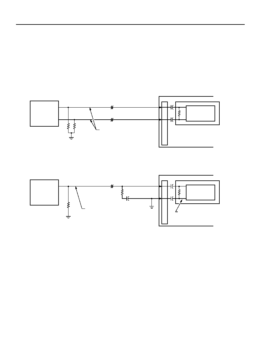
Figure 3, below, shows one example of the proper ter-
minations. Other methods may be used, provided they
meet the requirements stated above.
1-1054(F)
Figure 3. Transponder Interfacing
TxD[0:15]P
130
80
80
130
3.3 V
130
80
80
130
3.3 V
SONET/SDH
RxLINE
TxLINE
50
IMPEDANCE
CA16-TYPE TRANSPONDER
TRANSMISSION LINES
50
IMPEDANCE
TRANSMISSION LINES
INTERFACE IC
CO
NNE
CT
OR
(LVPECL)
TxD[0:15]N
(LVPECL)
RxD[0:15]P
(LVPECL)
RxD[0:15]N
(LVPECL)
MUX
DEMUX
Tx
Rx
14
14
Agere Systems Inc.
CA16-Type 2.5 Gbits/s DWDM Transponder with
Advance Data Sheet
16-Channel 155 Mbits/s Multiplexer/Demultiplexer
March 2001
Functional Description
(continued)
Transponder Interfacing
(continued)
TxR
EF
C
LK
P/N
The T
X
R
EF
C
LK
input is different than the other inputs to
the transmitter because it is internally terminated, ac-
coupled, and self-biased. Therefore, it must be treated
differently than the T
X
D and PIC
LK
inputs. Differentially,
the input impedance at this input is 100
, but due to
the way it is biased internally, when driven single-
ended, the impedance appears as 60
. The proper
termination scheme for the T
X
R
EF
C
LK
input is shown in
Figure 4.
Figure 4. Interfacing to the TxRefClk Input
INTERFACE
IC
(V
CC
= 3.3 V)
PLL
CLOCK
SYNTHESIZER
MULTIPLEXER
CA16 TRANSPONDER
TXREFCLKP
TXREFCLKN
50
TRANSMISSION LINES
DIFFERENTIAL INTERFACE
CONNE
CT
OR
10
0
33
0
33
0
SONET/SDH
INTERFACE
IC
(V
CC
= 3.3 V)
PLL
CLOCK
SYNTHESIZER
MULTIPLEXER
CA16 TRANSPONDER
TXREFCLKP
TXREFCLKN
50
TRANSMISSION LINES
SINGLE-ENDED INTERFACE
CONNE
CT
OR
60
33
0
0.1
µ
F
30
0
FOR A SINGLE-ENDED INPUT,
THE INPUT IMPEDANCE IS
EQUIVALENT TO 60
.
SONET/SDH
LVPECL
LVPECL
1-1084 (F).c

15
Agere Systems Inc.
Advance Data Sheet
CA16-Type 2.5 Gbits/s DWDM Transponder with
March 2001
16-Channel 155 Mbits/s Multiplexer/Demultiplexer
Optical Characteristics
Minimum and maximum values specified over operating case temperature range at 50% duty cycle data signal.
Typical values are measured at room temperature unless otherwise noted.
Table 4. OC-48/STM-16 Transmitter Optical Characteristics (Tc = 0 ∞C to 65 ∞C)
1. Output power definitions and measurements per ITU-T Recommendation G.957.
2. Full spectral width measured 20 dB down from the central wavelength peak under fully modulated conditions.
3. Ratio of the average output power in the dominant longitudinal mode to the power in the most significant side mode under fully modulated
conditions.
4. Ratio of logic 1 output power to logic 0 output power under fully modulated conditions.
5. GR-253-CORE, Synchronous Optical Network (SONET) Transport Systems: Common Generic Criteria.
6. ITU-T Recommendation G.957, Optical Interfaces for Equipment and Systems Relating to the Synchronous Digital Hierarchy.
Table 5. OC-48/STM-16 Receiver Optical Characteristics (Tc = 0 ∞C to 65 ∞C)
1. At 1310 nm, 1 x 10
≠10
BER, 2
23
≠ 1 pseudorandom data input.
Parameter
Symbol
Min
Typ
Max
Unit
Average Output Power:
1
Long Reach (1.55 µm DFB laser)
P
o
≠2
0
3
dBm
Operating Wavelength:
Long Reach (1.55 µm DFB laser);
All 48 100 GHz ITU Grid Channels Available
1528
--
1563
nm
Variation in Center Wavelength Over Operating
Temperature (EOL)
≠0.06
--
0.06
nm
Spectral Width:
Long Reach (DFB laser)
2
20
--
--
1
nm
Side-mode Suppression Ratio (DFB laser)
3
SSR
30
--
--
dB
Extinction Ratio
4
r
e
8.2
--
--
dB
Optical Rise and Fall Time:
CA16A2-Type
CA16B2-Type
t
R
, t
F
--
--
--
--
140
130
ps
ps
Dispersion Penalty:
CA16A2-Type
CA16B2-Type
DP
--
--
--
--
2.0
2.0
dB
dB
Eye Mask of Optical Output
5, 6
Compliant with GR-253 and ITU-T G.957
Jitter Generation
Compliant with GR-253 and ITU-T G.958
Parameter
Symbol
Min
Typ
Max
Unit
Average Receiver Sensitivity
1
:
APD Receiver
P
RMIN
≠29
≠34
--
dBm
Maximum Optical Power:
APD Receiver (long reach)
P
RMAX
≠8
≠6
--
dBm
Link Status Switching Threshold:
APD Decreasing Light Input
LSTD
--
TBD
--
dBm
Link Status Response Time
--
3
--
100
µs
Optical Path Penalty
--
--
--
2
dB
Receiver Reflectance
--
--
--
≠27
dB
Jitter Tolerance and Jitter Transfer
Compliant with GR-253 and ITU-T G.958

16
Agere Systems Inc.
CA16-Type 2.5 Gbits/s DWDM Transponder with
Advance Data Sheet
16-Channel 155 Mbits/s Multiplexer/Demultiplexer
March 2001
Electrical Characteristics
Table 6. Power Supply Characteristics (Tc = 0 ∞C to 65 ∞C)
Table 7. Transmitter Electrical I/O Characteristics (T
C
= 0 ∞C to 65 ∞C, V
CC
= 3.3 V ± 5%)
1. 20% to 80%.
2. Internally biased and ac-coupled.
3. The transmitter is normally enabled and only requires an external voltage to disable.
4. The WDEA alarm becomes active when the optical wavelength deviates from the nominal center wavelength by more than 100 pm.
5. Set at 500 mV at nominal optical output power. Provides linear P
O
tracking (≠3 dB = 250 mV, +3 dB = 1000 V).
6. Terminated into 200
to GND and 100
line-to-line.
Parameter
Symbol
Min
Typ
Max
Unit
Supply Voltage
V
CC
3.13
3.3
3.47
V
dc Power Supply Current Drain
I
CC
--
2000
--
mA
TEC Voltage
V
TEC
3.0
3.3
3.5
V
TEC-Only Current Drain
TEC_I
CC
--
0.6
1200
mA
Power Dissipation
P
DISS
--
<9
--
W
Parameter
Symbol
Logic
Min
Typ
Max
Unit
Parallel Input Clock
PIC
LK
P/N
Diff.
LVPECL
153.90
155.52
157.00
MHz
Parallel Clock in Duty Cycle
--
--
40
--
60
%
Reference Clock Freq. Tolerance
TxR
EF
C
LK
P/N
Diff.
LVPECL
≠20
--
20
ppm
Reference Clock Input Duty Cycle
--
--
30
--
70
%
Reference Clock Rise and Fall Time
1
t
R
, t
F
--
--
--
0.5
ns
Reference Clock Signal Levels
2
:
Differential Input Signal Level,
V
INDIFF
Single-ended Input Sig. Level,
V
INSINGLE
Differential Input Resistance,
R
TxR
EF
C
LK
Diff.
LVPECL
300
150
80
--
--
100
1200
600
120
mV
mV
Input Data Signal Levels:
Input High, V
IH
Input Low, V
IL
Input Voltage Swing,
V
IN
TxD[0:15]P/N
Diff.
LVPECL
V
CC
≠ 1.2
V
CC
≠ 2.0
300
--
--
--
V
CC
≠ 0.3
V
CC
≠ 1.5
--
V
V
mV
Transmitter Disable Input
3
TxD
IS
TTL (5 V)
2.0
--
5.0
V
Transmitter Enable Input
3
TxE
N
TTL (5 V)
0
--
0.8
V
Wavelength-Select Voltage:
Channel N Select, V
N
Channel N ≠ 1 Select, V
N≠1
WS
TTL
0
2.0
--
--
0.8
V
CC
V
V
Wavelength Deviation Alarm:
Normal Mode, V
NO-ALARM
Wavelength Alarm, V
ALARM
Alarm Setting (active-high)
4
WDEA
TTL
0
4.5
≠100
--
--
--
0.3
5
100
V
V
pm
Laser Degrade Alarm:
Normal Mode, V
NO-ALARM
Laser Degraded, V
ALARM
LSRALM
TTL
4.5
0
--
--
5
0.3
V
V
Laser Power Monitor Output
5
LPM
Analog
35
500
1000
mV
Phase Initialization:
Input High, V
IH
Input Low, V
IL
PHINIT
LVPECL
V
CC
≠ 1.0
V
CC
≠ 2.3
--
--
V
CC
≠ 0.57
V
CC
≠ 1.44
V
V

17
Agere Systems Inc.
Advance Data Sheet
CA16-Type 2.5 Gbits/s DWDM Transponder with
March 2001
16-Channel 155 Mbits/s Multiplexer/Demultiplexer
Electrical Characteristics
(continued)
1. 20% to 80%.
2. Internally biased and ac-coupled.
3. The transmitter is normally enabled and only requires an external voltage to disable.
4. The WDEA alarm becomes active when the optical wavelength deviates from the nominal center wavelength by more than 100 pm.
5. Set at 500 mV at nominal optical output power. Provides linear P
O
tracking (≠3 dB = 250 mV, +3 dB = 1000 V).
6. Terminated into 200
to GND and 100
line-to-line.
Table 8. Receiver Electrical I/O Characteristics (Tc = 0 ∞C to 65 ∞C, Vcc = 3.3 V ± 5%)
1. Terminated into 330
to ground.
2. 20% to 80%, 330
to ground.
Table 7. Transmitter Electrical I/O Characteristics (T
C
= 0 ∞C to 65 ∞C, V
CC
= 3.3 V ± 5%) (continued)
Parameter
Symbol
Logic
Min
Typ
Max
Unit
Phase Error
5
:
Output High, V
OH
Output Low, V
OL
PHERR
LVPECL
V
CC
≠ 1.2
V
CC
≠ 2.2
--
--
V
CC
≠ 0.65
V
CC
≠ 1.5
V
V
Line Loopback Enable:
Active-low:
Input High, V
IH
Input Low, V
IL
L
LOOP
LVTTL
2.0
0
--
--
V
CC
+ 1.0
0.8
V
V
Diagnostic Loopback Enable:
Active- low:
Input High, V
IH
Input Low, V
IL
D
LOOP
LVTTL
2.0
0
--
--
V
CC
+ 1.0
0.8
V
V
Parallel Output Clock
6
:
Output High, V
OH
Output Low, V
OL
Differential Voltage Swing,
V
DIFF
S-E Voltage Swing,
V
SINGLE
PC
LK
P/N
Differential
LVPECL
V
CC
≠ 1.15
V
CC
≠ 1.95
800
400
--
--
--
--
V
CC
≠ 0.6
V
CC
≠ 1.45
1900
950
V
V
mV
mV
Parameter
Symbol
Logic
Min
Typ
Max
Unit
Parallel Output Clock:
Output High, V
OH
Output Low, V
OL
POC
LK
P/N
Differential
LVPECL
V
CC
≠ 1.3
V
CC
≠ 2.0
--
--
V
CC
≠ 0.7
V
CC
≠ 1.4
V
V
POC
Lk
Duty Cycle
--
--
40
--
60
%
Output Data Signal Levels
1
:
Output High, V
OH
Output Low, V
OL
RxQ[0:15]P/N
Differential
LVPECL
V
CC
≠ 1.3
V
CC
≠ 2.0
--
--
V
CC
≠ 0.7
V
CC
≠ 1.4
V
V
RxQ[0:15] Rise/Fall Time
2
--
--
--
--
1.0
ns
Frame Pulse:
Output High, V
OH
Output Low, V
OL
FP
LVPECL
V
CC
≠ 1.3
V
CC
≠ 2.0
--
--
V
CC
≠ 0.7
V
CC
≠ 1.4
V
V
Loss-of-Signal Output:
Output High, V
OH
Output Low, V
OL
LOS
LVTTL
2.4
0
--
--
V
CC
0.4
V
V
Out-of-Frame Input:
Input High, V
IH
Input Low, V
IL
OOF
LVTTL
2.0
0.0
--
--
TTL V
CC
+ 1.0
0.8
V
V
Frame Enable Input
Input High, V
IH
Input Low, V
IL
FRAMEN
LVTTL
2.0
0.0
--
--
TTL V
CC
+ 1.0
0.8
V
V

18
18
Agere Systems Inc.
CA16-Type 2.5 Gbits/s DWDM Transponder with
Advance Data Sheet
16-Channel 155 Mbits/s Multiplexer/Demultiplexer
March 2001
Timing Characteristics
Transmitter Data Input Timing
The CA16 transponder utilizes a unique FIFO to
decouple the internal and external (PIC
LK
) clocks. The
FIFO can be initialized, which allows the system
designer to have an infinite PC
LK
-to-PIC
LK
delay
through this interfacing logic (ASIC or commercial chip
set). The configuration of the FIFO is dependent upon
the I/O pins, which comprise the synch timing loop.
This loop is formed from PHERR to PHINIT and PC
LK
to PIC
LK
.
The FIFO can be thought of as a memory stack that
can be initialized by PHINT or LOCKDET. The PHERR
signal is a pointer that goes high when a potential tim-
ing mismatch is detected between PIC
LK
and the inter-
nally generated PC
LK
clock. When PHERR is fed back
to PHINIT, it initializes the FIFO so that it does not over-
flow or underflow.
The internally generated divide-by-16 clock is used to
clock-out data from the FIFO. PHINIT and LOCKDET
signals will center the FIFO after the third PIC
LK
pulse.
This is done to ensure that PIC
LK
is stable. This
scheme allows the user to have an infinite PC
LK
to
PIC
LK
delay through the ASIC. Once the FIFO is cen-
tered, the PC
LK
and PIC
LK
can have a maximum drift of
±5 ns.
During normal operation, the incoming data is passed
from the PIC
LK i
nput timing domain to the internally
generated divide-by-16 PC
LK
timing domain. Although
the frequency of PIC
LK
and PC
LK
is the same, their
phase relationship is arbitrary. To prevent errors caused
by short setup or hold times between the two domains,
the timing generator circuitry monitors the phase rela-
tionship between PIC
LK
and PC
LK
.
When an FIFO timing violation is detected, the phase
error (PHERR) signal pulses high. If the condition per-
sists, PHERR will remain high. When PHERR is fed
back into the PHINIT input (by shorting them on the
printed-circuit board [PCB]), PHINIT will initialize the
FIFO if PHINIT is held high for at least two byte clocks.
The initialization of the FIFO prevents PC
LK
and PIC
LK
from concurrently trying to read and write over the
same FIFO bank.
During realignment, one-to-three bytes (16 bits wide)
will be lost. Alternatively, the customer logic can take in
the PHERR signal, process it, and send an output to
the PHINIT input in such a way that only idle bytes are
lost during the initialization of the FIFO. Once the FIFO
has been initialized, PHERR will go inactive.
19
Agere Systems Inc.
Advance Data Sheet
CA16-Type 2.5 Gbits/s DWDM Transponder with
March 2001
16-Channel 155 Mbits/s Multiplexer/Demultiplexer
Timing Characteristics
(continued)
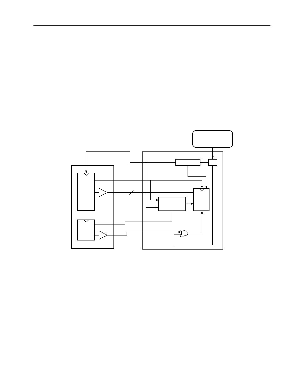
Input Timing Mode 1
In the configuration shown in Figure 5, PHERR to
PHINIT has a zero delay (shorted on the PCB) and the
PC
LK
is used to clock 16-bit-wide data out of the cus-
tomer ASIC. The FIFO in the multiplexer ia 16-bits wide
and six registers deep.
The PC
LK
and PIC
LK
signals respectively control the
READ and WRITE counters for the FIFO. The data
bank from the FIFO has to be read by the internally
generated clock (PC
LK
) only once after it has been writ-
ten by the PIC
LK
input.
Since the delay in the customer ASIC is unknown, the
two clocks (PC
LK
and PIC
LK
) might drift in respect to
each other and try to perform the read and writer oper-
ation on the same bank in the FIFO at the same time.
However, before such a clock mismatch can occur,
PHERR goes high and, if externally connected to
PHINIT, will initialize the FIFO provided PHINIT
remains high for at least two byte clocks. One to three
16-bit words of data will be lost during the initialization
of the FIFO.
Figure 5. Block Diagram Timing Mode 1
CUSTOMER LOGIC
CA16 TRANSPONDER
FIFO
PLL
DIVIDER
OSCILLATOR
T
X
REFCLK
16
PHERR
PHINIT
PCLK
PICLK
LOCKDET
155.52 MHz
±
20 ppm
TIMING
GENERATOR
INTERNAL
TXD[0:15]
CLOCK
DATA
CENTERS
FIFO
PCLK
D
Q
1-1121(F).b
20
20
Agere Systems Inc.
CA16-Type 2.5 Gbits/s DWDM Transponder with
Advance Data Sheet
16-Channel 155 Mbits/s Multiplexer/Demultiplexer
March 2001
Transmitter Data Input Timing
(continued)
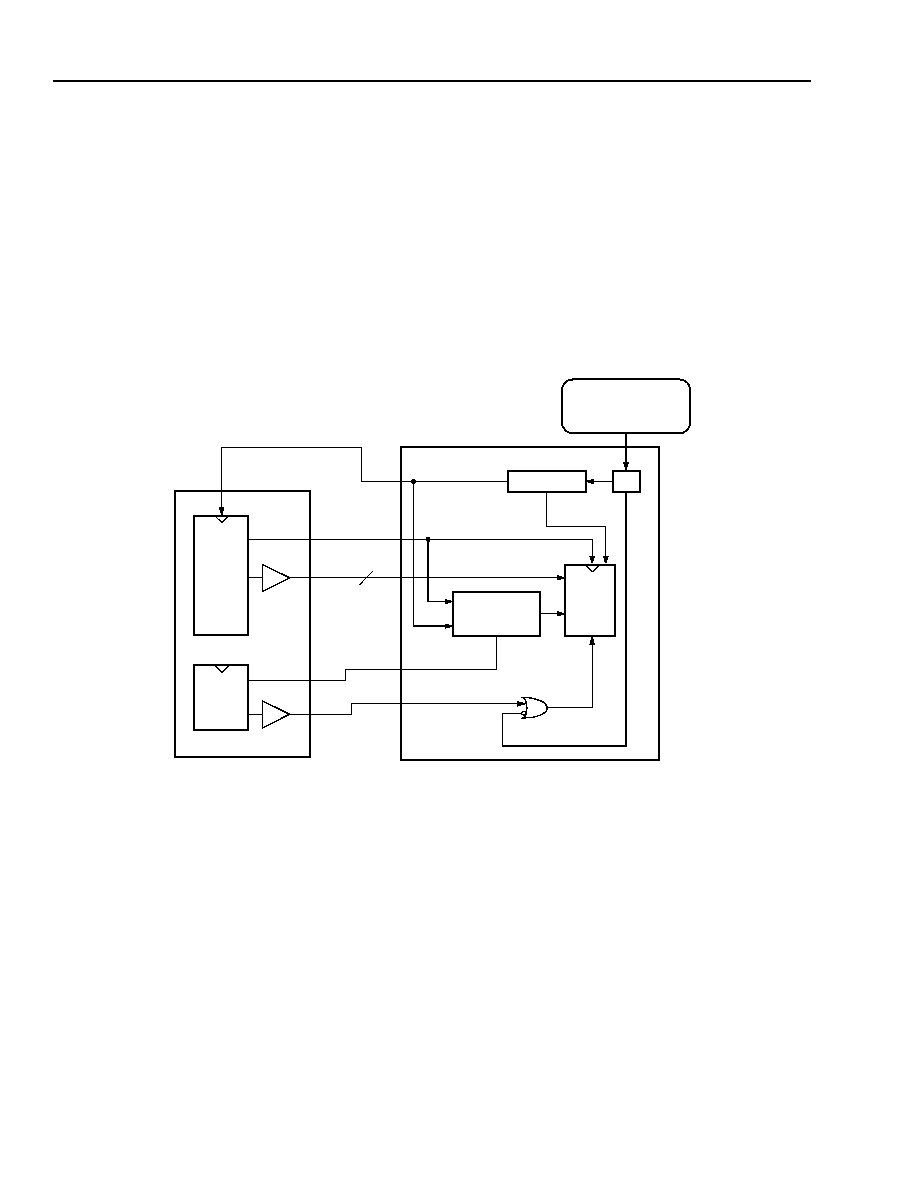
Input Timing Mode 2
To avoid the loss of data, idle or dummy bytes should
be sent on the T
X
D[0:15] bus whenever PHERR goes
high. In the configuration shown in Figure 6, the
PHERR signal is used as an input to the customer
logic. Upon detecting a high on the PHERR signal, the
customer logic should return a high signal, one that
remains high for at least two byte-clock cycles, to the
PHINIT input of the CA16. Also, when PHERR goes
high, the customer logic should start sending idle or
dummy bytes to the CA16 on the T
X
D[0:15] bus. This
should continue until PHERR goes low.
The FIFO is initialized two-to-eight byte clocks after
PHINIT goes high for two byte clocks. PHERR goes low
after the FIFO is initialized. Upon detecting a low on
PHERR, the customer logic can start sending real data
bytes on T
X
D[0:15]. The two timing loops (PC
LK
to
PIC
LK
and PHERR to PHINIT) do not have to be of
equal length.
Figure 6. Block Diagram Timing Mode 2
CUSTOMER LOGIC
CA16 TRANSPONDER
FIFO
PLL
DIVIDER
OSCILLATOR
T
X
REFCLK
16
PHERR
PHINIT
PCLK
PICLK
LOCKDET
155.52 MHz
±
20 ppm
TIMING
GENERATOR
INTERNAL
TXD[0:15]
CLOCK
DATA
CENTERS
FIFO
PCLK
D
Q
1121(F).b
21
Agere Systems Inc.
Advance Data Sheet
CA16-Type 2.5 Gbits/s DWDM Transponder with
March 2001
16-Channel 155 Mbits/s Multiplexer/Demultiplexer
Timing Characteristics
(continued)
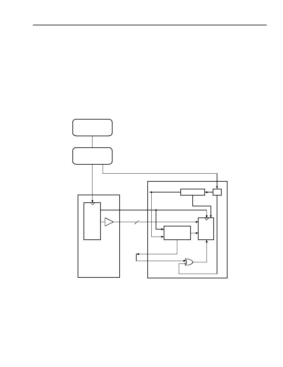
Forward Clocking
In some applications, it is necessary to forward-clock
the data in a SONET/SDH system. In this application,
the reference clock from which the high-speed serial
clock is synthesized and the parallel data clock both
originate from the same source on the customer appli-
cation circuit. The timing control logic in the CA16 tran-
sponder transmitter automatically generates an internal
load signal that has a fixed relationship to the reference
clock. The logic takes into account the variation of the
reference clock to the internal load signal over temper-
ature and voltage. The connections required to imple-
ment this clocking method are shown in Figure 7. The
setup and hold times for PIC
LK
to TxD[0:15] must be
met by the customer logic.
Possible problems: to meet the jitter generation specifi-
cations required by SONET/SDH, the jitter of the refer-
ence clock must be minimized. It could be difficult to
meet the SONET jitter generation specifications using
a reference clock generated from the customer logic.
Figure 7. Forward Clocking of the CA16 Transponder
CUSTOMER LOGIC
CA16 TRANSPONDER
FIFO
PLL
DIVIDER
T
X
REFCLK
16
PHERR
PHINIT
PCLK
PICLK
LOCKDET
TIMING
GENERATOR
INTERNAL
TXD[0:15]
CLOCK
DATA
CENTERS
FIFO
PCLK
OSCILLATOR
155.52 MHz
±
20 ppm
T
X
REFCLK
CLOCK
BUFFER
1-1122(F).a
22
22
Agere Systems Inc.
CA16-Type 2.5 Gbits/s DWDM Transponder with
Advance Data Sheet
16-Channel 155 Mbits/s Multiplexer/Demultiplexer
March 2001
Timing Characteristics
(continued)
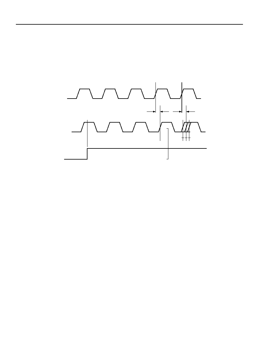
PC
LK
-to-PIC
LK
Timing
After powerup or RESET, the LOCKDET signal will go
active, signifying that the PLL has locked to the clock
provided on the T
X
R
EF
C
LK
input. The FIFO is initialized
on the third PIC
LK
after LOCKDET goes active. The
PC
LK
-to-PIC
LK
delay (t
D
) can have any value before the
FIFO is initialized. The t
D
is fixed at the third PICLK
after LOCKDET goes active. Once the FIFO is initial-
ized, PC
LK
and PIC
LK
cannot drift more than 5.2 ns;
tCH cannot be more than 5.2 ns.
Figure 8. PC
LK
-to-PIC
LK
Timing
PCLK
PICLK
LOCKDET
ACTIVE
3RD
IS INITALIZED AT THE THIRD RISING EDGE OF
PICLK AFTER LOCKDET GOES ACTIVE.
PCLK-TO-PICLK DELAY IS FIXED AND FIFO
2ND
1ST
tCH
tCH
tD
tD
1-1123(F)
23
Agere Systems Inc.
Advance Data Sheet
CA16-Type 2.5 Gbits/s DWDM Transponder with
March 2001
16-Channel 155 Mbits/s Multiplexer/Demultiplexer
Timing Characteristics
(continued)
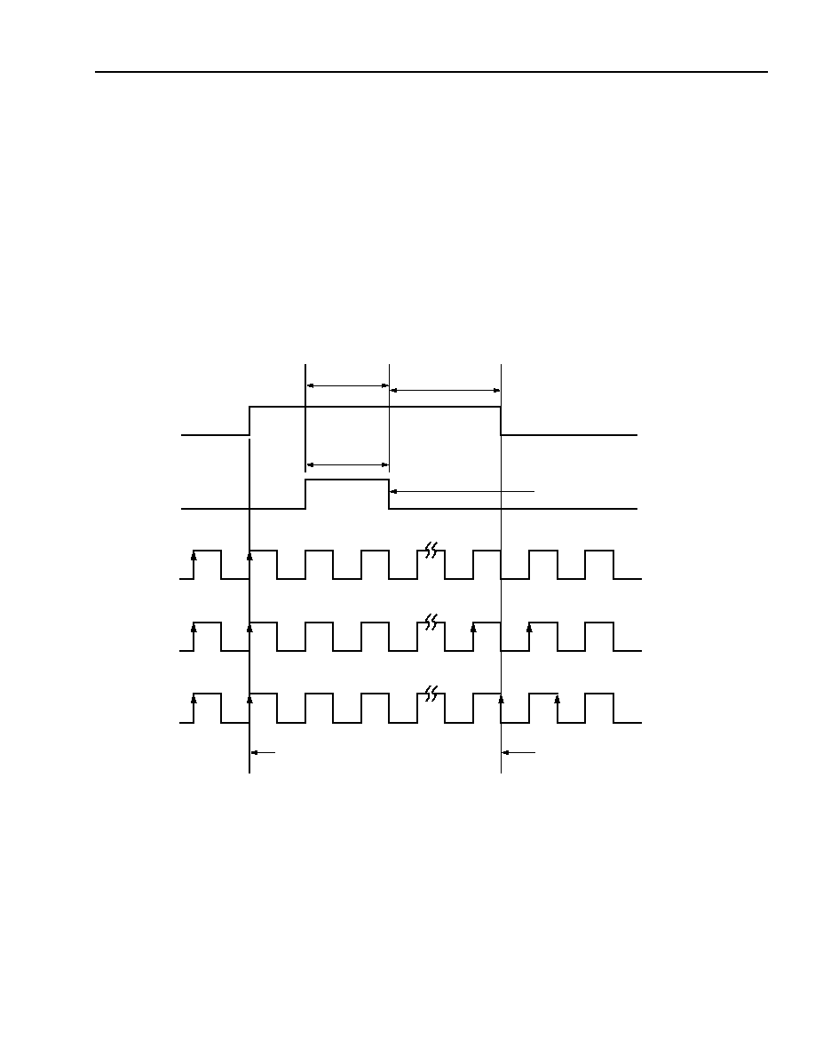
PHERR/PHINIT
Case 1--PHERR and PHINIT are shorted on the
printed-circuit board:
PHINIT would go high whenever there is a potential tim-
ing mismatch between PC
LK
and PIC
LK
. PHINIT would
remain high as long as the timing mismatch between
PC
LK
and PIC
LK
. If PHINIT is high for more than two
byte clocks, the FIFO will be initialized. PHINIT will ini-
tialize the FIFO two-to-eight byte clocks after it is high
for at least two byte clocks, PHERR (and thus PHINIT)
goes active once the FIFI is initialized.
Case 2--PHERR signal is input to the customer logic
and the customer logic outputs a signal to PHINIT:
Another possible configuration is where the PHERR
signal is input into the customer logic and the customer
logic sends an output to the PHINIT input. However,
the customer logic must ensure that, upon detecting a
high on PHERR, the PHINIT signal remains high for
more than two byte clocks. If PHINIT is high for less
than two byte clocks, the FIFO is not guaranteed to be
initialized. Also, the customer logic must ensure that
PHINIT goes low after the FIFO is initialized (PHERR
goes low).
Figure 9. PHERR/PHINIT Timing
PHERR
PHINIT
PCLK
PICLK
INTERNAL
PCLK
MINIMUM PULSE
WIDTH REQUIRED
TO CENTER
THE FIFO
2 BYTE
CLOCKS
2--8 BYTE CLOCKS
CUSTOMER ASIC SENDS A
MINIMUM PULSE WIDTH OF
2 BYTE CLOCKS UPON DETECTING
A HIGH ON PHERR
FIFO IS INITIALIZED 2--8 BYTE CLOCKS
AFTER PHINIT IS HIGH FOR 2 BYTE CLOCKS
PHERR GOES HIGH ON
DETECTING A FIFO TIMING ERROR
1125(F)
24
Agere Systems Inc.
CA16-Type 2.5 Gbits/s DWDM Transponder with
Advance Data Sheet
16-Channel 155 Mbits/s Multiplexer/Demultiplexer
March 2001
Timing Characteristics
(continued)
T
ransmitter Data Input Timing
(continued)
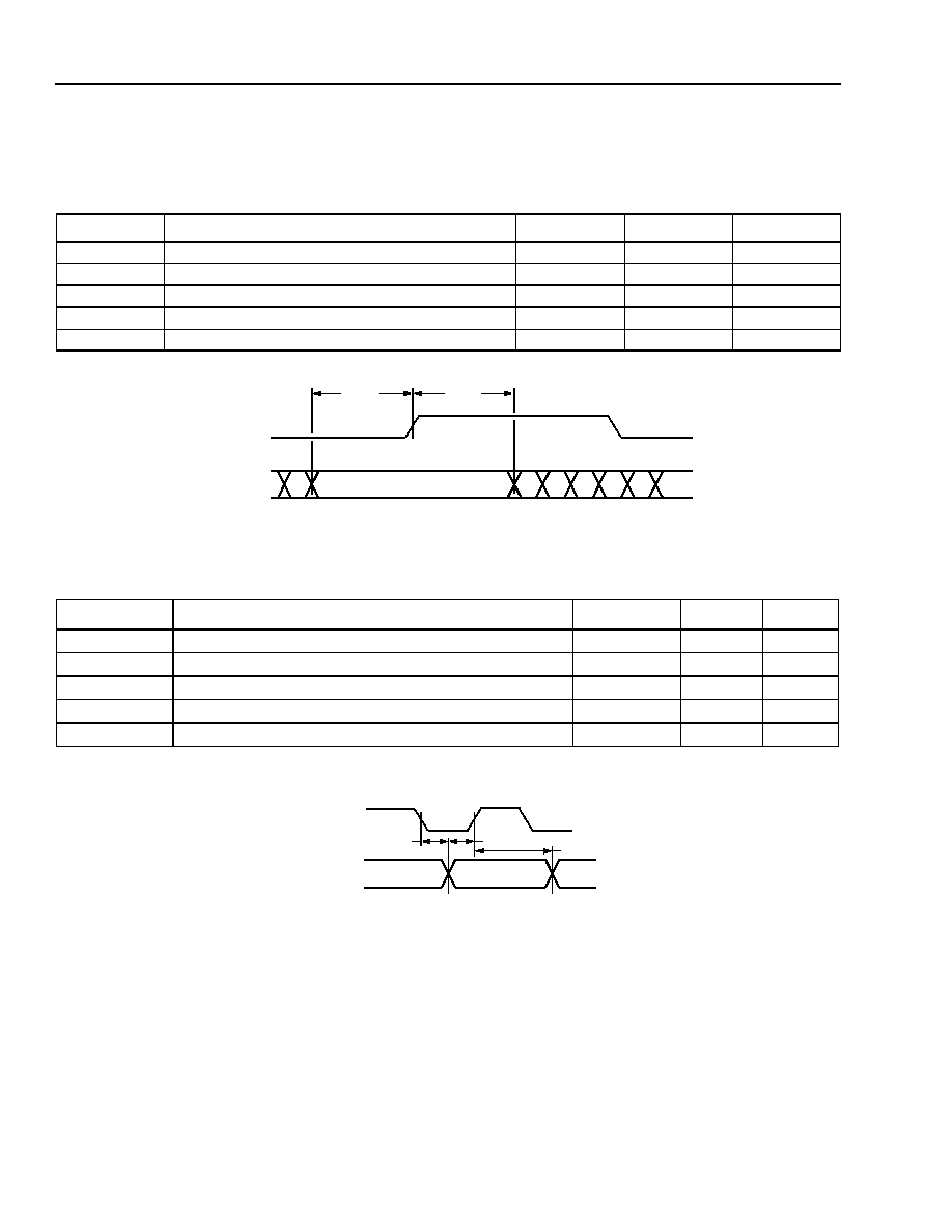
Figure 10. ac Input Timing
1. 20% to 80%; 330
to GND.
Figure 11. Receiver Output Timing Diagram
Table 9. Transmitter ac Timing Characteristics
Symbol
Description
Min
Max
Unit
t
ST
X
D
TxD[0:15] Setup Time w. r. t. PIC
LK
1.5
--
ns
t
HT
X
D
TxD[0:15] Hold Time w. r. t. PIC
LK
0.5
--
ns
--
PC
LK
P/N Duty Cycle
40
55
%
--
PIC
LK
P/N Duty Cycle
40
60
%
t
PPIC
LK
PIC
LK
-to-PIC
LK
Drift After FIFO Centered
--
5
ns
Table 10. Receiver ac Timing Characteristics
Symbol
Description
Min
Max
Unit
--
POC
LK
Duty Cycle
45
55
%
--
RxD[15:0] Rise and Fall Time
1
--
1.0
ns
tP
POUT
POC
LK
Low to RxD[15:0] Valid Propagation Delay
≠1
1
ns
tS
POUT
RxD[15:0] and FP Setup Time w. r. t. POC
LK
2
--
ns
tH
POUT
RxD[15:0] and FP Hold Time w. r. t. POC
LK
2
--
ns
PICLKP
TXD[0:15]
t
STXD
t
HTXD
POCLKP
FP
tP
POUT
tS
POUT
tH
POUT
RXD[15:0]
25
Agere Systems Inc.
Advance Data Sheet
CA16-Type 2.5 Gbits/s DWDM Transponder with
March 2001
16-Channel 155 Mbits/s Multiplexer/Demultiplexer
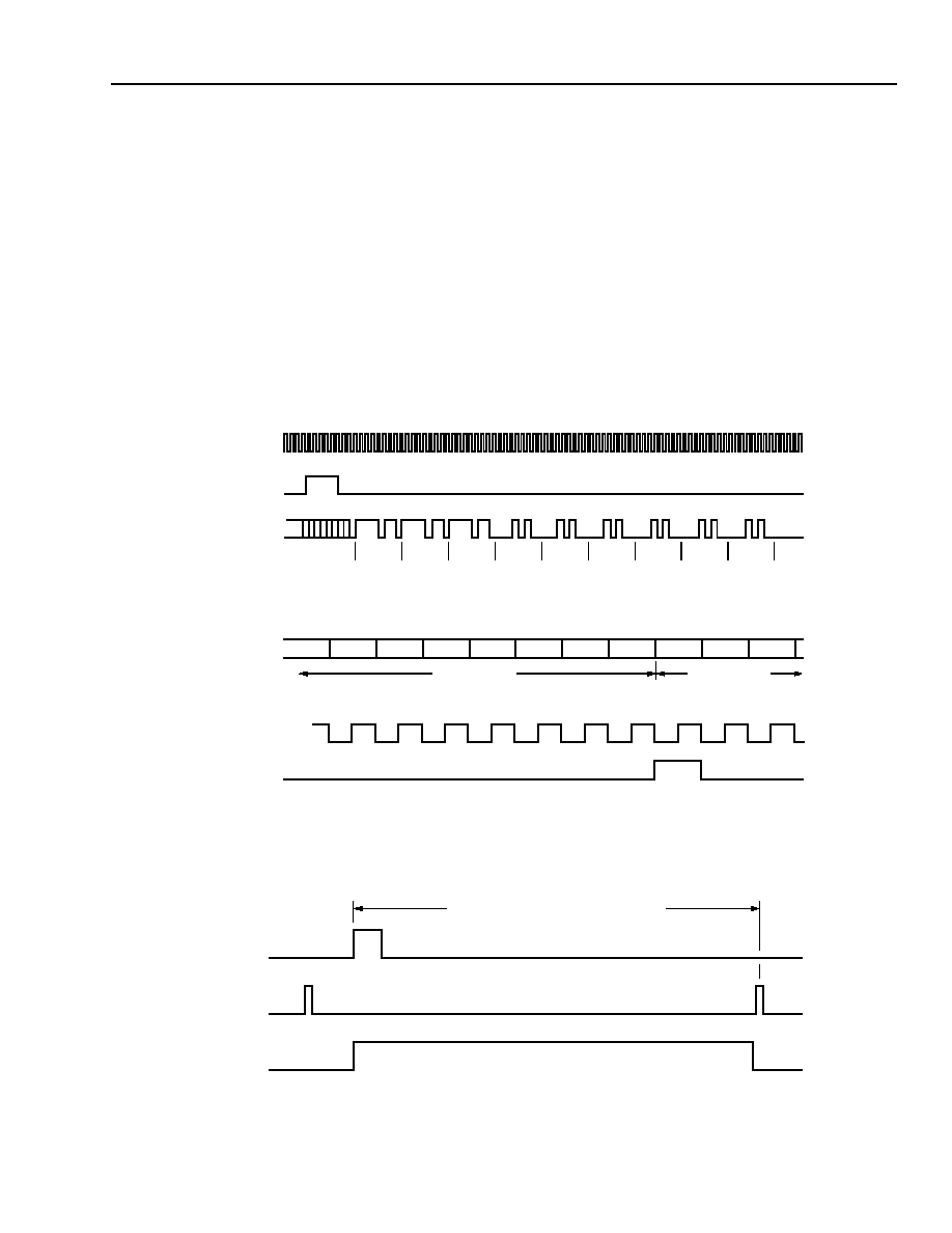
Figure 12. Frame and Byte Detection
1-1024(F)
Figure 13. OOF Timing (FRAMEN = High)
RECOVERED
CLOCK
OOF
SERIAL
DATA
RXD[15:0]
ROCLK
A1
A1
A1
A2
A2
A2
A2
A2
A2
A1, A1
A1, A1
A1, A1
A2, A2
A2, A2
A2, A2
A2, A2
INVALID DATA
VALID DATA
FP
OOF
FP
SEARCH
BOUNDARY DETECTION ENABLED
Timing Characteristics
(continued)
Receiver Framing
Note: Future versions of the cooled transponder
will not support the frame-detect function.
Figure 12 shows a typical reframe sequence in which a
byte realignment is made. The frame and byte bound-
ary detection is enabled by the rising edge of OOF.
Both the frame and byte boundaries are recognized
upon receipt of the first A2 byte following three consec-
utive A1 bytes. The third A2 byte is the first data byte to
be reported with the correct byte alignment on the out-
going data bus (RxD[15:0]). Concurrently, the frame
pulse (FP) is set high for one POC
LK
cycle.
The frame and byte boundary detection block is acti-
vated by the rising edge of OOF and stays active until
the first FP pulse.
Figure 13 shows the frame and byte boundary detec-
tion activation by a rising edge of OOF and deactiva-
tion by the first FP pulse.
Figure 14 shows the frame and byte boundary detec-
tion by the activation of a rising edge of OOF and deac-
tivation by the FRAMEN input.
1-1023(F)r.3
26
Agere Systems Inc.
CA16-Type 2.5 Gbits/s DWDM Transponder with
Advance Data Sheet
16-Channel 155 Mbits/s Multiplexer/Demultiplexer
March 2001
Timing Characteristics
(continued)
1-1025(F)
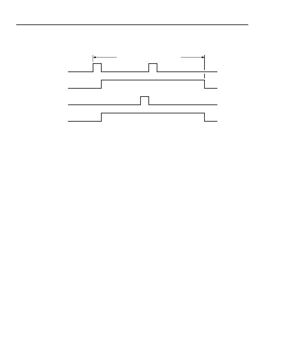
Figure 14. FRAMEN Timing
Wavelength Selection
When the wavelength select (WS) pin is at a logic low or open circuited, the optical wavelength from the CA16
transmitter will be a nominal wavelength as determined by the device code purchased. If the WS pin is pulled high
(logic 1), the optical wavelength will change to the next lower ITU channel number (100 GHz spacing,
will
increase approximately 0.8 nm).
During the wavelength change, the transmitter's optical output will be disabled and the wavelength deviation error
alarm will be active until the wavelength has stabilized at its new value. The LSRALM will also be active (logic 1)
during the wavelength change process.
BOUNDARY DETECTION ENABLED
OOF
FRAMEN
FP
SEARCH

27
Agere Systems Inc.
Advance Data Sheet
CA16-Type 2.5 Gbits/s DWDM Transponder with
March 2001
16-Channel 155 Mbits/s Multiplexer/Demultiplexer
Qualification and Reliability
To help ensure high product reliability and customer satisfaction, Agere Systems Inc. is committed to an intensive
quality pro-gram that starts in the design phase and proceeds through the manufacturing process. Optoelectronics
modules are qualified to Agere internal standards using MIL-STD-883 test methods and procedures and using
sampling techniques consistent with Telcordia Technologies
* requirements. This qualification program fully meets
the intent of Telcordia Technologies reliability practices TR-NWT-000468 and TA-TSY-000983. In addition, the
Agere Optoelectronics design, development, and manufacturing facility has been certified to be in full compliance
with the latest ISO
9001 Quality System Standards.
* Telcordia Technologies is a trademark of Telcordia Technologies, Inc.
ISO is a registered trademark of The International Organization for Standardization.
Laser Safety Information
Class I Laser Product
All versions of the CA16-type transponders are classified as Class I laser products per FDA/CDRH, 21 CFR 1040
Laser Safety requirements. The transponders have been registered/certified with the FDA under accession number
8720009. All versions are classified as Class I laser products per IEC
825-1:1993.
CAUTION: Use of controls, adjustments, and procedures other than those specified herein may result in
hazardous laser radiation exposure.
This product complies with 21 CFR 1040.10 and 1040.11.
8.8
µ
m single-mode pigtail with connector.
Wavelength = 1.5
µ
m.
Maximum power = 2.0 mW.
Product is not shipped with power supply.
Because of size constraints, laser safety labeling is not affixed to the module but is attached to the outside of the
shipping carton.
NOTICE
Unterminated optical connectors can emit laser radiation.
Do not view with optical instruments.
Electromagnetic Emissions and Immunity
The CA16 transponder will be tested against CENELEC EN50 081 part 1 and part 2, FCC 15, Class B limits for
emissions.
The CA16 transponder will be tested against CENELEC EN50 082 part 1 immunity requirements.
IEC is a registered trademark of The International Electrotechnical Commission.
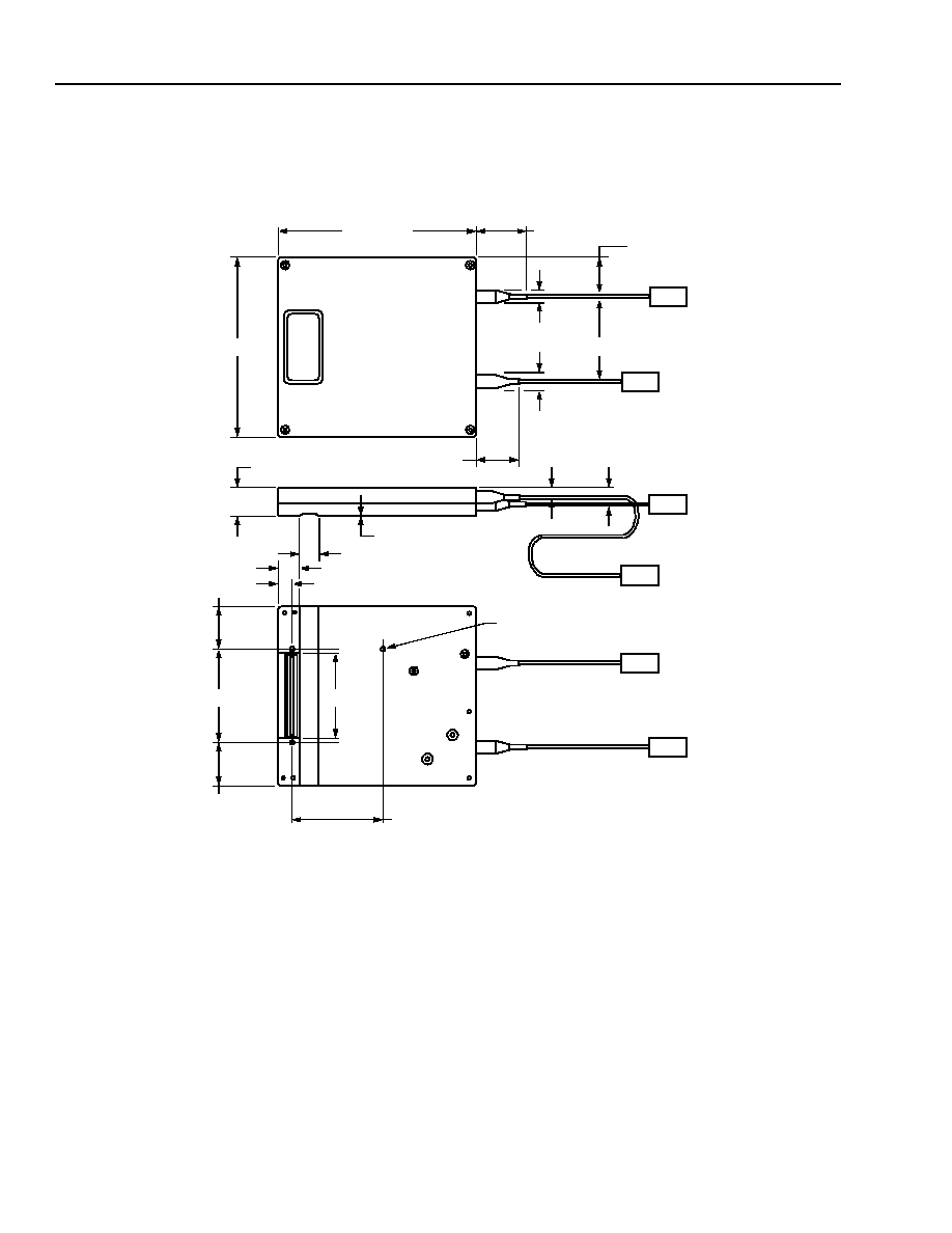
28
Agere Systems Inc.
CA16-Type 2.5 Gbits/s DWDM Transponder with
Advance Data Sheet
16-Channel 155 Mbits/s Multiplexer/Demultiplexer
March 2001
Outline Diagram
Dimensions are in inches and (millimeters) (for initial samples; production version will be slightly smaller).
1-1103(F)
4.00 (101.6)
3.50 (88.9)
1.02 (25.91)
0.76 (19.3)
0.25 (6.4)
1.65 (41.9)
0.87 (22.1)
0.55 (14.0)
0.015 (0.38)
0.20 (5.08)
0.29 (7.4)
0.17 (4.3)
0.45 (11.4)
0.30 (7.6)
0.83 (21.1)
1.84 (46.7)
0.83 (21.1)
1.70 (43.2)
1.80 (45.7)
(3x) M2.5 x 0.45 MOUNTING HOLES
2 mm MAXIMUM LENGTH INTO PACKAGE
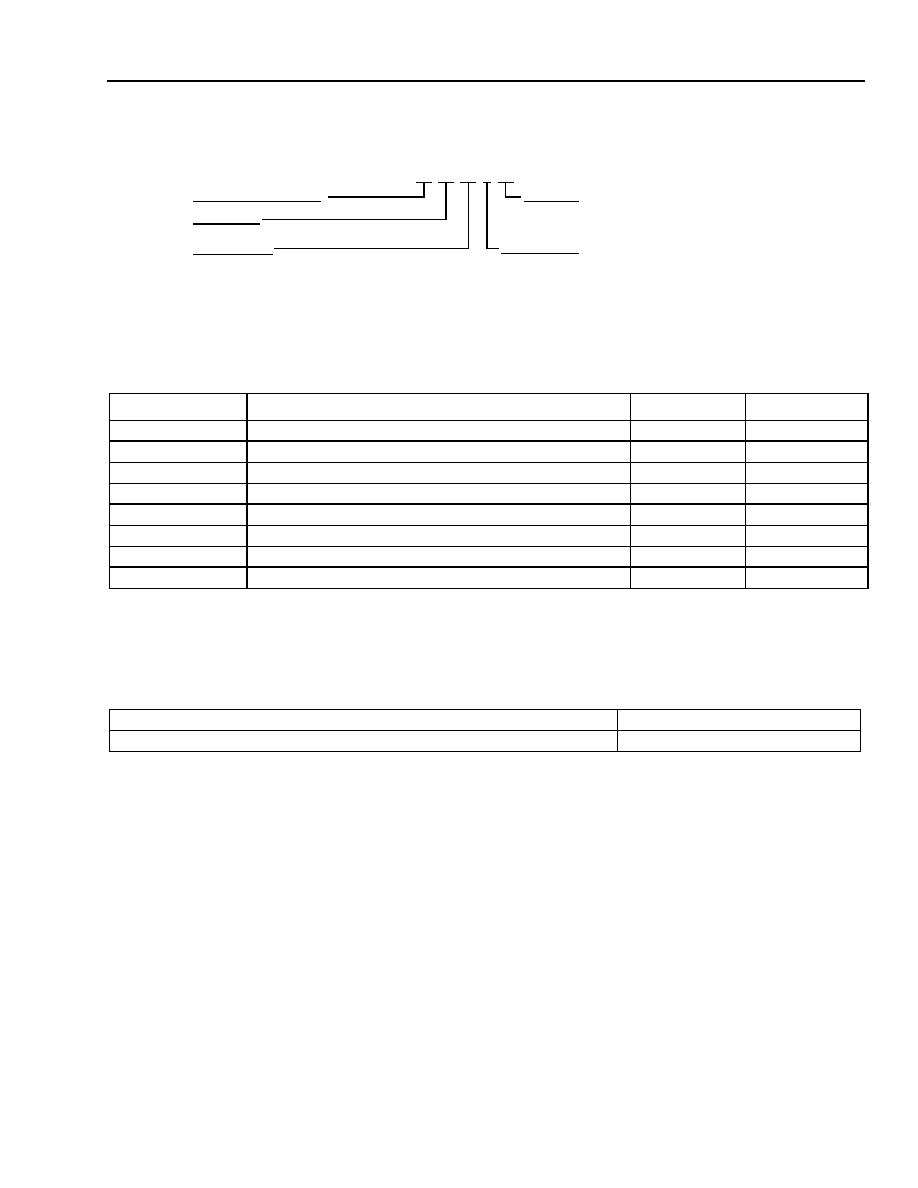
29
Agere Systems Inc.
Advance Data Sheet
CA16-Type 2.5 Gbits/s DWDM Transponder with
March 2001
16-Channel 155 Mbits/s Multiplexer/Demultiplexer
Ordering Information
* Other connectors may be made available.
Table 11. Ordering Information
For specific order codes for these products, please contact your local Agere account manager.
Related Product Information
Code
Application
Connector
Comcode
CA16A2CAA
Unspecified wavelength (1800 ps-nm)
SC
108701475
CA16A2FAA
Unspecified wavelength (1800 ps-nm)
FC/PC
108701483
CA16A2Cnn
Specified wavelength (1800 ps-nm)
SC
--
CA16A2Fnn
Specified wavelength (1800 ps-nm)
FC/PC
--
CA16B2CAA
Unspecified wavelength (3000 ps-nm)
SC
108701491
CA16B2FAA
Unspecified wavelength (3000 ps-nm)
FC/PC
108701509
CA16B2Cnn
Specified wavelength (3000 ps-nm)
SC
--
CA16B2Fnn
Specified wavelength (3000 ps-nm)
FC/PC
--
Table 12. Related Product Information
Description
Document Number
Using the Lucent Technologies Transponder Test Board Application Note
AP00-017OPTO
ORDER CODE:
16 XX X XX
CA
≠
≠
≠
BASIC PART NUMBER
STM LEVEL
APPLICATION
16 = STM-16 (SONET OC-48)
A2 = 1800 ps-nm (100 km)
OPTIONS
CONNECTOR*
C = SC
F = FC
B2 = 3000 ps-n (170 km)
AA = Unspecified
17--61 = ITU frequency (191.7 THz--196.1 THz)

Agere Systems Inc. reserves the right to make changes to the product(s) or information contained herein without notice. No liabi lity is assumed as a result of their use or application. ST is a
registered trademark of Agere Systems Inc.
Copyright © 2001 Agere Systems Inc.
All Rights Reserved
Printed in U.S.A.
March 2001
DS01-120OPTO (Replaces DS99-352LWP)
For additional information, contact your Agere Systems Account Manager or the following:
INTERNET:
http://www.agere.com
E-MAIL:
docmaster@agere.com
N. AMERICA:
Agere Systems Inc., 555 Union Boulevard, Room 30L-15P-BA, Allentown, PA 18109-3286
1-800-372-2447, FAX 610-712-4106 (In CANADA: 1-800-553-2448, FAX 610-712-4106)
ASIA:
Agere Systems Hong Kong Ltd., Suites 3201 & 3210-12, 32/F, Tower 2, The Gateway, Harbour City, Kowloon
Tel. (852) 3129-2000, FAX (852) 3129-2020
CHINA: (86) 21-5047-1212 (Shanghai), (86) 10-6522-5566 (Beijing), (86) 755-695-7224 (Shenzhen)
JAPAN: (81) 3-5421-1600 (Tokyo), KOREA: (82) 2-767-1850 (Seoul), SINGAPORE: (65) 778-8833, TAIWAN: (886) 2-2725-5858 (Taipei)
EUROPE:
Tel. (44) 7000 624624, FAX (44) 1344 488 045