 | –≠–ª–µ–∫—Ç—Ä–æ–Ω–Ω—ã–π –∫–æ–º–ø–æ–Ω–µ–Ω—Ç: DNC3X3625 | –°–∫–∞—á–∞—Ç—å:  PDF PDF  ZIP ZIP |

Advance Data Sheet
March 2000
4
Features
Hex 10 Mbits/s Transceiver
s
DSP based.
s
Compatible with
IEEE
* 802.3 10Base-T standard
for twisted-pair cable.
s
Half- and full-duplex operations.
s
Autopolarity detection and correction.
s
Adjustable squelch level for extended wire-length
capability (two levels).
s
Interfaces with
IEEE
802.3u media independent
interface (MII) or a serial 10 Mbits/s 7-pin interface.
s
On-chip filtering eliminates the need for external fil-
ters.
Hex 100 Mbits/s Transceiver
s
Compatible with
IEEE
802.3u MII (clause 22),
PCS/PMA (clause 24), PMD (clause 25), MII man-
agement, and autonegotiation (clause 28) specifi-
cations.
s
Selectable 5-bit code-group (PDT/PDR interface)
or 4-bit data nibbles (MII interface) input/output.
s
Full- or half-duplex operations.
s
Optional carrier integrity monitor (CIM).
s
Selectable carrier sense signal generation (MCRS)
asserted during either transmission or reception in
half duplex (MCRS asserted during reception only
in full duplex).
s
Adaptive equalization and baseline wander correc-
tion.
s
On-chip filtering eliminates the need for external
filters.
*
IEEE
is a registered trademark of The Institute of Electrical and
Electronics Engineers, Inc.
Hex 100 Mbits/s FX Transceiver
s
Compatible with
IEEE
802.3u 100Base-FX stan-
dard.
s
Reuses existing twisted-pair I/O pins for compatible
fiber-optic transceiver pseudo-ECL (PECL) data.
s
Fiber mode automatically configures port:
-- FX mode enable is pin or register selectable
-- Disables autonegotiation and 10Base-T.
-- Enables 100Base-FX remote fault signaling.
-- Disables MLT-3 encoder/decoder.
-- Disables scrambler/descrambler.
General
s
Ports individually configurable
s
Autonegotiation and management:
-- Fast link pulse (FLP) burst generator.
-- Arbitration function.
-- Accepts preamble suppression.
-- Operates up to 12.5 MHz.
s
Supports the MII station management protocol and
frame format (clause 22): basic and extended reg-
ister set.
s
Supports next page.
s
Provides status signals: receive activity, transmit
activity, full duplex, collision/jabber, link integrity,
and speed indication.
s
Powerdown mode for 10 Mbits/s and 100 Mbits/s
operation.
s
Loopback testing for 10 Mbits/s and 100 Mbits/s
operation.
s
0.25
µ
m low-power CMOS technology.
s
Single 3.3 V power supply operation.
s
25 MHz XTAL oscillator input or 25 MHz/50 MHz/
125 MHz clock input.
s
Compatible with RMII (standard version) and SMII
(standard version).
Note: Advisories are issued as needed to update product information. When using this data sheet for design purposes, please contact
your Lucent Technologies Microelectronics Group Account Manager to obtain the latest advisory on this product.
DNC3X3625
Hex 10/100 Mbits/s Ethernet Transceiver Macrocell

DNC3X3625
Advance Data Sheet
10/100 Mbits/s Ethernet Transceiver Macrocell
March 2000
2
Table of Contents
Contents
Page
Features .................................................................................................................................................................... 1
Hex 10 Mbits/s Transceiver ..................................................................................................................................... 1
Hex 100 Mbits/s Transceiver ................................................................................................................................... 1
Hex 100 Mbits/s FX Transceiver.............................................................................................................................. 1
General ................................................................................................................................................................... 1
Description ................................................................................................................................................................ 4
Functional Block Diagram ....................................................................................................................................... 4
Macrocell I/Os ......................................................................................................................................................... 5
Signal Information...................................................................................................................................................... 6
Signal Descriptions ................................................................................................................................................. 6
MII Station Management ......................................................................................................................................... 13
Basic Operation .................................................................................................................................................... 13
MII Interface Design ................................................................................................................................................ 14
Absolute Maximum Ratings.....................................................................................................................................14
Electrical Characteristics ......................................................................................................................................... 15
Register Information ................................................................................................................................................ 19
Register Descriptions............................................................................................................................................ 19
Application Notes: Board Layout ............................................................................................................................. 31
Board Layout Considerations ................................................................................................................................ 31
Tables
Page
Table 1. MII/5-Bit Serial Interface Signals................................................................................................................. 6
Table 2. MII Management Signals ............................................................................................................................ 7
Table 3. 10/100 Mbits/s Twisted-Pair (TP) Interface Signals..................................................................................... 7
Table 4. Status Signals ............................................................................................................................................. 8
Table 5. Clock and Reset Signals ............................................................................................................................. 9
Table 6. Control/Status Signals .............................................................................................................................. 10
Table 7. Testability Signals...................................................................................................................................... 12
Table 8. MII Management Frame Format................................................................................................................ 13
Table 9. MII Management Frames--Field Description............................................................................................ 13
Table 10 . Absolute Maximum Ratings ...................................................................................................................14
Table 11 . Operating Conditions ............................................................................................................................. 14
Table 12. Summary of Management Registers (MR) ............................................................................................. 19
Table 13. MR0--Control Register Bit Descriptions ................................................................................................. 20
Table 14. MR1--Status Register Bit Descriptions .................................................................................................. 21
Table 15. MR2, MR3--PHY Identification Registers (1 and 2) Bit Descriptions ..................................................... 22
Table 16. MR4--Autonegotiation Advertisement Register Bit Descriptions............................................................ 22
Table 17. MR5--Autonegotiation Link Partner Ability (Base Page) Register Bit Descriptions ................................ 23
Table 18. MR5--Autonegotiation Link Partner (LP) Ability Register (Next Page) Bit Descriptions ......................... 23
Table 19. MR6--Autonegotiation Expansion Register Bit Descriptions .................................................................. 24
Table 20. MR7--Next Page Transmit Register Bit Descriptions.............................................................................. 25
Table 21. MR16--PCS Control Register Bit Descriptions....................................................................................... 25
Table 22. MR17--Autonegotiation Read Register A...............................................................................................26
Table 23. MR18--Autonegotiation Read Register B...............................................................................................26
Table 24. MR20--User-Defined Register ............................................................................................................... 27
Table 25. MR21--RXER Counter ........................................................................................................................... 27

Table of Contents
(continued)
Tables
(continued)
Page
Advance Data Sheet
DNC3X3625
March 2000
10/100 Mbits/s Ethernet Transceiver Macrocell
3
Table 26. MR28--Device-Specific Register 1 (Status Register) Bit Descriptions ...................................................27
Table 27. MR29--Device-Specific Register 2 (100 Mbits/s Control) Bit Descriptions.............................................28
Table 28. MR30--Device-Specific Register 3 (10 Mbits/s Control) Bit Descriptions...............................................29
Table 29. MR31--Device-Specific Register 4 (Quick Status) Bit Descriptions .......................................................30
Figures
Page
Figure 1. DNC3X3625 Functional Block Diagram .................................................................................................... 4
Figure 2. I/Os of the DNC3X3625 Macrocell ............................................................................................................ 5
Figure 3. DNC MII TX Logic ...................................................................................................................................15
Figure 4. DNC MII RX Logic ...................................................................................................................................15
Figure 5. DNC Maintenance Logic .........................................................................................................................15
Figure 6. Typical Application (One Channel Shown) ..............................................................................................16
Figure 7. Pinout Assignment ..................................................................................................................................17
Figure 8. Typical Single-Channel Twisted-Pair (TP) Interface.................................................................................18
4
DNC3X3625
Advance Data Sheet
10/100 Mbits/s Ethernet Transceiver Macrocell
March 2000
4
Description
The DNC3X3625 is a twisted-pair transceiver macrocell that supports transmission and reception over category 3
unshielded twisted-pair (UTP) cable and category 5 UTP.
The DNC3X3625 has been designed specifically for applications that support both 10Base-T and 100Base-X, such
as network interface cards (NICs), switches.
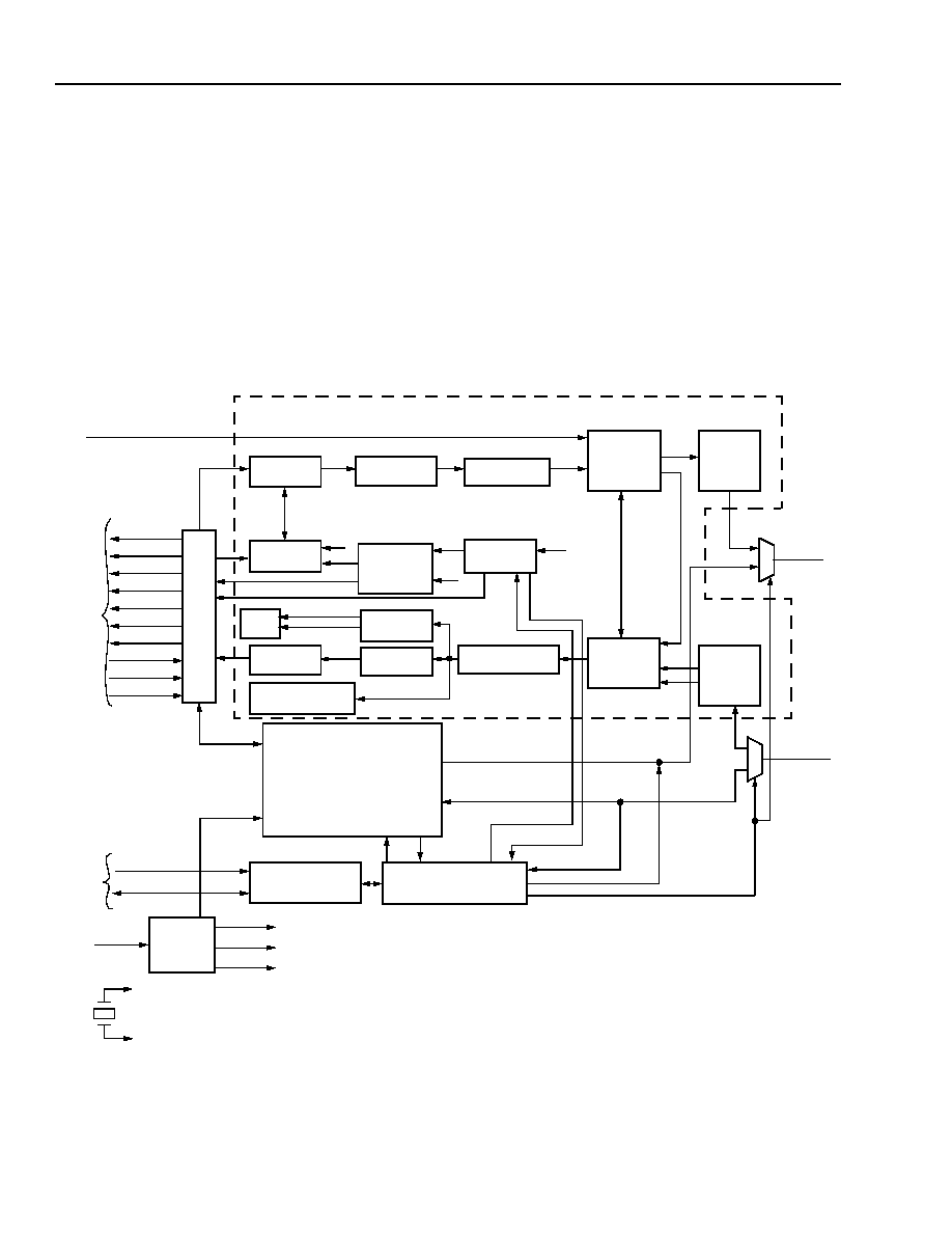
Figure 1 represents a functional block diagram of the DNC3X3625 macrocell.
Figure 2 shows the I/Os of the DNC3X3625 macrocell.
Functional Block Diagram
5-5136(F).j
Figure 1. DNC3X3625 Functional Block Diagram (1 Channel Shown)
TPI
±
TPO
±
AUTONEGOTIATION
AND LINK MONITOR
MTXD[3:0]
4B/5B
ENCODER
FAR-END
FAULT GEN.
SCRAMBLER
PDT
SD
PDR/
DESCRAMBLER
ALIGNER
5B/4B
DECODER
FAR-END
FAULT DETECT
10 Mbits/s TRANSCEIVER
CLK20
MDC
MDIO
MII
TX STATE
MACHINE
SD
COLLISION
DETECT
SD
RX STATE
MACHINE
MII
MTX_ER
MTX_EN
MTXD[3:0]
MTXCLK
MRXCLK
MRX_ER
MRX_DV
MRXD[3:0]
MCOL
MCRS
MANAGEMENT
25 MHz
125 MHz
RMCLK
PMD
TX
PMD
RX
SD
100 Mbits/s TRANSCEIVER
LC10 LS10
LC100
LS100
CARRIER
CIM
DETECT
RXERR_ST
CAR_STAT
MI
I
I
N
TE
RF
ACE
SERIAL/PARALLEL
INTERFACE
FREQ.
125 MH
Z
MA
NAG
E
M
E
N
T
IN
T
E
R
F
A
C
E
20 MHz
25 MHz
CRYSTAL
DCRU
SYNTH.

Advance Data Sheet
DNC3X3625
March 2000
10/100 Mbits/s Ethernet Transceiver Macrocell
5
4
Description
(continued)
Macrocell I/Os
5-7541(F).a.r2
Figure 2. I/Os of the DNC3X3625 Macrocell
APFE_PIN[7:0]
AUTO_EN[7:0]
CARIN_IN[7:0]
CRS_SEL[7:0]
EDBT[7:0]
ELLE_PIN[7:0]
EN_RMCK
EN_XTL
FASTSEL[1:0]
FASTTEST
FX_MODE[7:0]
F_DUP[7:0]
HBT_PIN[7:0]
IN125
INT_MASK[7:0]
ISOLATE[7:0]
LITF_ENH
LPBK_PIN[7:0]
MDC
MDIO_IN
MGT_ADD[4:2]
MODEL[5:0]
MTXD[3:0][7:0]
MTX_EN[7:0]
MTX_ER[7:0]
NOLP_PIN[7:0]
OUI[24:3]
POR
PWRDN[7:0]
RMCLK
SDBT[7:0]
SDFX[7:0]
SECUR[7:0]
SER_SEL_PIN[7:0]
SPEED_PIN[7:0]
TESTMDC
TESTMDIN
TESTSEL[3:0]
TESTTXD[3:0]
TESTTXEN
TESTTXER
TPI[7:0]
TPIB[7:0]
VERSION[3:0]
XLO
HWRESET
ATBON
ATBOP
AUTODONE[7:0]
CLK25RAW
CS[7:0]
ECLN
ECLP
FDUP_OUT[7:0]
INT_R31[7:0]
LS100_OK[7:0]
LS10_OK[7:0]
MCOL[7:0]
MCRS[7:0]
MDIO_HI_Z
MDIO_OUT
MRXCLK[7:0]
MRXD[3:0][7:0]
MRX_DV[7:0]
MRX_ER[7:0]
MTXCLK[7:0]
REG20_OUT[15:0][7:0]
REXT10
REXT100
REXTBS
RMCLKRAW
RS[7:0]
RST_TX_BUSY[7:0]
RST_BUSY[7:0]
RST_10_BUSY[7:0]
SERIAL_SEL[7:0]
SLOWCLK[7:0]
TESTCOL[7:0]
TESTCRS[7:0]
TESTMDHZ
TESTMDOUT
TESTRXCK[7:0]
TESTRXDV[7:0]
TESTRXD[3:0][7:0]]
TESTRXER[7:0]
TESTTXCK[7:0]
TPAPS[7:0]
TPJS[7:0]
TPO[7:0]
TPOB[7:0]
XHI
XS[7:0]
LS_OK[7:0]
LED_STR_EN
LED_BLINK_EN
DNC3X3825
BYPPD125
BYPPD160
CK125_BUF
CK125P
CK160
REV_ADD

6
DNC3X3625
Advance Data Sheet
10/100 Mbits/s Ethernet Transceiver Macrocell
March 2000
4
Signal
Information
Signal Descriptions
Table 1. MII/5-Bit Serial Interface Signals
Signal
Type
Name/Description
MCOL[5:0]
O
Collision Detect. This signal signifies in half-duplex mode that a collision has occurred on
the network. MCOL is asserted high whenever there is transmit and receive activity on the
UTP media. MCOL is the logical AND of MTX_EN and receive activity, and is an asynchro-
nous output. When SER_SEL_PIN is high and in 10Base-T mode, MCOL indicates the
jabber timer has expired.
MCRS[5:0]
O
Carrier Sense. When CRS_SEL is low, this signal is asserted high when either the
transmit or receive medium is nonidle. This signal remains asserted throughout a collision
condition. When CRS_SEL is high, MCRS is asserted on receive activity only. CRS_SEL is
set via the MII management interface or the CRS_SEL signal.
MRXCLK
[5:0]
O
Receive Clock. 25 MHz clock output in 100 Mbits/s mode, 2.5 MHz output in 10 Mbits/s
nibble mode, and 10 MHz in 10 Mbits/s serial mode. MRXCLK has a worst-case 35/65 duty
cycle. MRXCLK provides the timing reference for the transfer of MRX_DV, MRXD, and
MRX_ER signals.
MRXD[3:0]
[5:0]
O
Receive Data. 4-bit parallel data outputs that are synchronous to MRXCLK. When
MRX_ER is asserted high in 100 Mbits/s mode, an error code will be presented on
MRXD[3:0] where appropriate. The codes are as follows:
Packet errors: ERROR_CODES = 2h.
Link errors: ERROR_CODES = 3h. (Packet and link error codes will only be repeated if
registers [29.9] and [29.8] are enabled.)
Premature end errors: ERROR_CODES = 4h.
Code errors: ERROR_CODES = 5h.
When SER_SEL_PIN is active-high and 10 Mbits/s mode is selected, MRXD[0] is used for
data output and MRXD[3:1] are 3-stated.
MRX_DV
[5:0]
O
Receive Data Valid. When this signal is high, it indicates the DNC3X3625 is recovering
and decoding valid nibbles on MRXD[3:0], and the data is synchronous with MRXCLK.
MRX_DV is synchronous with MRXCLK. This signal is not used in serial 10 Mbits/s mode.
MRX_ER
[5:0]
O
Receive Error. When high, MRX_ER indicates the DNC3X3625 has detected a coding
error in the frame presently being received. MRX_ER is synchronous with MRXCLK.
MTXCLK
[5:0]
O
Transmit Clock. 25 MHz clock output in 100 Mbits/s mode, 2.5 MHz output in 10 Mbits/s
MII mode, 10 MHz output in 10 Mbits/s serial mode. MTXCLK provides timing reference for
the transfer of the MTX_EN, MTXD, and MTX_ER signals sampled on the rising edge of
MTXCLK.
MTXD[3:0]
[5:0]
I
Transmit Data. 4-bit parallel input synchronous with MTXCLK. When SER_SEL_PIN is
active-high and 10 Mbits/s mode is selected, only MTXD[0] is valid.
MTX_EN
[5:0]
I
Transmit Enable. When driven high, this signal indicates there is valid data on MTXD[3:0].
MTX_EN is synchronous with MTXCLK. When SER_SEL_PIN is active-high and
10 Mbits/s mode is selected, this signal indicates there is valid data on MTXD[0].
MTX_ER
[5:0]
I
Transmit Coding Error. When driven high, this signal causes the encoder to intentionally
corrupt the byte being transmitted across the MII (00100 will be transmitted). When in
10 Mbits/s mode, this signal is ignored.

Advance Data Sheet
DNC3X3625
March 2000
10/100 Mbits/s Ethernet Transceiver Macrocell
7
4
Signal Information
(continued)
Table 2. MII Management Signals
Table 3. 10/100 Mbits/s Twisted-Pair (TP) Interface Signals
Signal
Type
Name/Description
MDC
I
Management Data Clock. This is the timing reference for the transfer of data
on the MDIO signal. This signal may be asynchronous to MRXCLK and
MTXCLK. The maximum clock rate is 12.5 MHz.
When running MDC above 6.25 MHz, MDC must be synchronous with
CLK25RAW and have a setup time of 15 ns and a hold time of 5 ns with respect
to CLK25RAW.
MDIO_IN
I
Management Data Input. Control information is driven by the station manage-
ment, synchronous with MDC, onto this input.
MDIO_OUT
O
Management Data Output. Status information is driven by the DNC3X3625,
synchronous with MDC, onto this output.
MDIO_HI_Z
O
Management Data Output Enable. When high, this signal can be used to
3-state the MDIO bidirectional buffer (external to the DNC3X3625).
INT_MASK[5:0]
I
Interrupt Mask. When set high, no interrupt is generated under any condition.
When set low, interrupts are generated according to bit [31.7]. This signal is
ORed with bit [31.6].
INT_R31[5:0]
O
Maskable Status Interrupt. This signal will go high whenever there is a change
in status as defined in Table 27.
Signal
Type
Name/Description
TPI
[5:0]
PADI
Received Data. Positive differential received 125 Mbaud MLT3 or 10 Mbaud
Manchester data from magnetics.
Fiber-Optic Data Input. Positive differential received 125 Mbaud pseudo-ECL
data from fiber transceiver.
TPIB
[5:0]
PADI
Received Data. Negative differential received 125 Mbaud MLT3 or 10 Mbaud
Manchester data from magnetics.
Fiber-Optic Data Input. Negative differential received 125 Mbaud pseudo-ECL
data from fiber transceiver.
TPO
[5:0]
PADO
Transmit Data. Positive differential transmit 125 Mbaud MLT3 or 10 Mbaud
Manchester data to magnetics.
Fiber-Optic Data Output. Positive differential transmit 125 Mbaud pseudo-ECL
compatible data to fiber transceiver.
TPOB
[5:0]
PADO
Transmit Data. Negative differential transmit 125 Mbaud MLT3 or 10 Mbaud
Manchester data to magnetics.
Fiber-Optic Data Output. Negative differential transmit 125 Mbaud pseudo-
ECL compatible data to fiber transceiver.
REXT10
PADO
Current Setting 10 Mbits/s. An external resistor (21.0 k
) is placed from this
signal to ground to set the 10 Mbits/s TP driver transmit output level.
REXT100
PADO
Current Setting 100 Mbits/s. An external resistor (21.5 k
) is placed from this
signal to ground to set the 100 Mbits/s TP driver transmit output level.
REXTBS
PADO
Band Gap Reference for the Receive Channel. Connect this signal to a
24.9 k
± 1% resistor to ground. The parasitic load capacitance should be less
than 15 pF.

8
DNC3X3625
Advance Data Sheet
10/100 Mbits/s Ethernet Transceiver Macrocell
March 2000
4
Signal Information
(continued)
LEDs operate as follows:
LED_STR_EN = 0, LED_BLINK_EN = 0 => No stretching/blinking.
LED_STR_EN = 1, LED_BLINK_EN = 0 => Stretch to 42 ms, minimum.
LED_STR_EN = 0, LED_BLINK_EN = 1 => Every activity causes 42 mS ON, 42 mS OFF blink.
LED_STR_EN = 1, LED_BLINK_EN = 1 => Every activity causes 0.5 second ON, 0.5 second OFF blink.
Table 4. Status Signals
Signal
Type
Name/Description
XS[5:0]
O
Transmit Status. This signal indicates transmit activity. This output can be
stretched or blinked per the description given above.
RS[5:0]
O
Receive Status. This signal indicates receive activity. This output can be
stretched or blinked per the description given above.
CS[5:0]
O
Collision Status. This signal indicates collision occurrence. This output can
be stretched or blinked per the description given above.
LS10_OK[5:0]
O
Link10. This signal indicates good link status for 10 Mbits/s.
LS100_OK[5:0]
O
Link100. This signal indicates good link status for 100 Mbits/s.
LS_OK[5:0]
O
Link Status. Indicates link status.
FDUP_OUT[5:0]
O
Full-Duplex Status. If this signal is high, it indicates full-duplex link, and if it is
low, then the link is half duplex.
TPJS[5:0]
O
Jabber Status. Indicates that there is a jabber condition (only in 10 Mbits/s).
TPAPS[5:0]
O
TP Autopolarity Status. Indicates if autopolarity has been detected and
corrected.

Advance Data Sheet
DNC3X3625
March 2000
10/100 Mbits/s Ethernet Transceiver Macrocell
9
4
Signal Information
(continued)
Table 5. Clock and Reset Signals
* Double bonded with XLO.
Double bonded with RMCLK.
Signal
Type
Name/Description
EN_RMCK
I
Enable RMCLK. When high, this signal selects RMCLK as the clock input.
This signal and EN_XTL cannot be high simultaneously.
RMCLK
PADI*
Primary Input Clock. The frequency of this clock can be either 125 MHz or
50 MHz. IN125 is used to indicate the appropriate frequency. This clock input
is used when EN_RMCK is high.
IN125
I
Input Clock Frequency Select. When high, this signal will indicate that the
frequency of RMCLK is 125 MHz; else the clock frequency is 50 MHz.
EN_XTL
I
Enable Crystal Input. This signal, when high, will select the crystal input
(XLO) as the clock input. This signal and EN_RMCK cannot be high simulta-
neously.
XLO
PADI
Crystal Oscillator Input. A 25 MHz crystal ± 25 ppm can be connected
across XLO and XHI. Alternately, a 25 MHz external CMOS oscillator can be
connected to this input. This clock input is used when EN_XTL is high.
XHI
PADO
(optional)
Crystal Oscillator Output. This pad does not have to be bonded out if crystal
is not used.
CLK25RAW
O
CLK25RAW. 25 MHz output clock.
RMCLKRAW
O
RMCLKRAW. Buffered version of the RMCLK. This is either 50 MHz or
125 MHz, depending on RMCLK frequency.
SLOWCLK[5:0]
O
24 Hz Clock Output. This is a 24 Hz output signal.
HWRESET
I
Full-Chip Reset. Reset is active-high. The RST_BUSY signal will go low
when reset is complete. 10Base-T and 100Base-TX/-FX are in reset until
enabled and take 1.3 ms to come out of reset.
POR
I
Power-On Reset. If a powerup reset (PUR) cell from ASIC library is not used,
then tie this input low.
RST_BUSY[5:0]
O
Reset Busy. This signal indicates that the DNC3X3625 is in reset.
RST_10_BUSY[5:0]
O
10Base-T in Reset. This signal indicates that the 10 Mbits/s logic is in reset.
RST_TX_BUSY[5:0]
O
100Base-TX Reset. This signal indicates that the 100 Mbits/s logic is in reset.
BYPPD125
I
This pin, when high, powers up the 125 MHz PLL permanently, allowing
CK125P to be used for external logic at all times.
BYPPD160
I
This pin, when high, powers up the 160 MHz PLL permanently, allowing
CK160 to be used for external logic at all times.
CK125_BUF
I
This pin is the feedback for CK125P. Normally this will be connected to
CK125P or any external chip clock buffers for CK125P.
CK160
O
This is a 160 MHz output clock; this will be available if 10Base-T is enabled or
BYPPD160 is high.
CK125P
O
This is a 125 MHz output clock, which must be fed back to CK125_BUF. This
will be available when in 100Base-Tx mode or if BYPPD125 is high or if IN125
is high.

10
DNC3X3625
Advance Data Sheet
10/100 Mbits/s Ethernet Transceiver Macrocell
March 2000
4
Signal Information
(continued)
Table 6. Control/Status Signals
Signal
Type Description
AUTO_EN[5:0]
I
Autonegotiation Enable. When this signal is high, autonegotiation is
enabled. Pulsing this signal will cause autonegotiation to restart. This input
has the same function as register 0, bit 12. This input and the register bit are
ANDed together.
F_DUP[5:0]
I
Full-Duplex Mode. When this signal is set high, the PHY will be in full-
duplex mode. A low on this signal will put it in half-duplex mode. This signal
is ignored when autonegotiation is enabled. This is the same function as
register 0, bit 8. This input and the register bit are ORed together.
CRS_SEL[5:0]
I
Carrier Sense Select. This signal may be used to select the mode of
MCRS operation. When this signal is pulled high, MCRS will be asserted on
receive activity only. This is the same function as register 29, bit 10. This
input and the register bit are ORed together.
SER_SEL_PIN[5:0]
I
Serial Mode Select. This signal may be used to set the SERIAL_SEL func-
tion of register 30, bit 1 by pulling it high, if station management is unavail-
able. This input and the register bit are ORed together.
CARIN_IN[5:0]
I
Carrier Integrity Enable. If this signal is pulled high, it will enable the
carrier integrity function of register 29, bit 3, if station management is
unavailable. This input and the register bit are ORed together.
EDBT[5:0]
I
Encoder/Decoder Bypass. If this signal is pulled high, it will enable the
encoder/decoder bypass function of register 29, bit 6, if station management
is unavailable. This input and the register bit are ORed together.
SDBT[5:0]
I
Scrambler/Descrambler. This signal may be used to enable the scrambler/
descrambler bypass function by pulling this signal high, if station manage-
ment is unavailable. This is the same function as register 29, bit 4. This
input and the register bit are ORed together.
SPEED_PIN[5:0]
I
Speed. This signal can be used to select the operating speed and is the
same function as register 0, bit 13:
s
If this signal is pulled high, it will enable 100 Mbits/s operation.
s
If this signal is pulled low, it will enable 10 Mbits/s operation.
This signal is ignored when autonegotiation is enabled. This signal and the
register bit are ANDed.
MGT_ADD[4:2]
I
Management Address [4:2]. These signals set the management
addresses and are decoded as follows:
MGT_ADD[4:2]
PHY 0, PHY 1, PHY 2, PHY 3, PHY 4, PHY 5
000
0, 1, 2, 3, 4, 5
001
8, 9, 10, 11, 12, 13
010
16, 17, 18, 19, 20, 21
011
24, 25, 26, 27, 28, 29
100
6, 7, 8, 9, 10, 11
101
12, 13, 14, 15, 16, 17
110
18, 19, 20, 21, 22, 23
111
0, 0, 0, 0, 0, 0, 0, 0
REV_ADD
I
Reverse Phy Address. Reverse the order of Ports for Management
Access. (PHY0 is highest address, PHY5 is lowest address)
FX_MODE[5:0]
I
FX_MODE. When this signal is high, it puts DNC3X3625 in fiber-optic
mode. This signal is ORed with register 29, bit 0 [29.0].

Advance Data Sheet
DNC3X3625
March 2000
10/100 Mbits/s Ethernet Transceiver Macrocell
11
4
FASTTEST
I
Fast Test. This signal should be low for normal operation. When high, the
internal timers run faster than normal, with the speedup determined by
FASTSEL[1:0]
FASTSEL[1:0]
I
Fast Speed Select. When FASTTEST is high, the speedup of the timers
(10 Mbit/s NLP link, 10 Mbit/s jabber, reset timers, autonegotiation counters)
is as follows:
00 = No speedup.
01 = 16x speedup.
10 = 64x speedup.
11 = 256x speedup. (Autonegotiation does not work at this speedup.)
LITF_ENH
I
Enhanced Link Integrity Test Function. When this input is high, The link
will be deasserted when 31 Manchester violations have occurred.
SDFX[5:0]
PAD
(optional I)
SDFX. Signal detect from fiber-optic receiver. This pad does not have to be
bonded out if fiber mode is not used.
SECUR[5:0]
I
Security. When this input is high and MTX_EN is high, JAM pattern (55) is
transmitted.
ISOLATE[5:0]
I
Isolate. When this signal is high, the macrocell will come out of reset in
isolate mode per the
IEEE
standard. If this is low, then the macrocell will
come out of reset in normal mode. When isolated, all receive outputs are
low, and all transmit requests are ignored. While isolated, the macrcell will
respond to management transactions, detect, and transmit link pulses.
Register 0, bit 10, is used to put the transceiver in/out of isolate mode.
APFE_PIN[5:0]
I
Autopolarity Function Enable (Active Low). When this signal is set low
and the DNC3X3625 is operating at 10 Mbits/s, the autopolarity function will
determine if the TP link is wired with a polarity reversal:
s
The DNC3X3625 will assert the autopolarity status (APS) bit (register 28,
bit 6) and correct the polarity reversal.
s
If this signal is set high and the DNC3X3625 is operating at 10 Mbits/s,
the reversal will not be corrected.
ELLE_PIN[5:0]
I
Extended Line Length Enable. When this signal is set high, the receive
squelch level is reduced from a nominal 435 mV to 350 mV, allowing recep-
tion of signals with lower amplitude. This is the same function as register 30,
bit 4. The input and the register bit are ORed together.
HBT_PIN[5:0]
I
Heartbeat Enable. When asserted high, this input will enable the heartbeat
function (serial mode). This is the same function as register 30, bit 5. The
input and the register bit are ORed together.
LPBK_PIN[5:0]
I
Loopback. When this signal is asserted high DNC3X3625 is in loopback
mode. No data transmission will take place on the media and any receive
data will be ignored. This is the same function as register 0, bit 14. The input
and the register bit are ORed together.
NOLP_PIN[5:0]
I
No Link Pulse Mode. Setting this signal high will allow 10 Mbits/s operation
with link pulses disabled. If the DNC3X3625 is configured for
100 Mbits/s operation, this signal is ignored. This is the same function as
register 30, bit 0. The input and the register bit are ORed together.
LED_STR_EN
I
LED Stretch Enable. This pin, when low, disables stretching. When high,
the LED output is stretched to 42 ms minimum, unless LED_BLINK_EN is
high. This signal is ORed with register 29, bit 7.
Signal
Type Description
Signal Information
(continued)
Table 6. Control/Status Signals (continued)

12
DNC3X3625
Advance Data Sheet
10/100 Mbits/s Ethernet Transceiver Macrocell
March 2000
4
Table 7. Testability Signals
LED_BLINK_EN
I
LED Blink Enable. This pin, when low, disables blinking. When high, the
LED output will blink high for 42 ms and low for 42 ms whenever there is
activity, unless LED_STR_EN is high, in which case the blinking is 0.5
seconds high and 0.5 seconds low. This signal is ORed with register 29, bit
11.
OUI[24:3]
I
Organizationally Unique Identifier. This can be programmed by the user,
upon instantiation of the macro.
MODEL[5:0]
I
Model Number. 6-bit model number of the device. This can be programmed
upon instantiation.
VERSION[3:0]
I
Revision Number. The value of the present revision number. This can be
programmed upon instantiation.
PWRDN[5:0]
I
Powerdown. When high, this signal powers down the PHY and resets all
management registers.
SERIAL_SEL[5:0]
O
Serial Select. When this signal is high, it indicates 10 Mbit/s serial mode.
When SERIAL_SEL is low, the macro is in 100 Mbits/s or 10 Mbits/s parallel
mode.
AUTODONE[5:0]
O
Autonegotiation Done. This signal goes high whenever autonegotiation
has completed. It will go low if autonegotiation has to restart.
RG20_OUT[15:0]
[5:0]
O
Register 20 Access. This bus provides access to the user-defined register.
A write to this register can be through MDIO.
Signal
Type
Description
TESTSEL[3:0]
I
Test Mode Select. These pins enable the PHY to be in various test
modes: scan, analog, etc. Lucent requires access to these pins for
manufacturing testing. They should be held low for normal operation.
TESTMDC
I
Test Mode Inputs. These test inputs provide a high level of controlla-
bility to the macrocell, either as scan inputs or as digital/analog test
inputs/controls depending on the test mode selected by TESTSEL[3:0].
TESTTXD[3:0]
TESTTXER
TESTTXEN
TESTCRS[5:0]
O
Test Mode Outputs. These test output pins provide observability in the
form of either scan outputs or digital/analog test outputs depending on
the test mode selected by TESTSEL[3:0]. The TESTRXD[3:0][5:0] and
TESTRXER[5:0] must be mapped to outputs during test. The other test
output should be mapped, if possible, to ease PHY debugging.
TESTCOL[5:0]
TESTRXCK[5:0]
TESTTXCK[5:0]
TESTRXD[3:0][5:0]
TESTRXER[5:0]
TESTRXDV[5:0]
ATBOP
PADO
(optional)
Analog Test Output Pins. These are used in Lucent test modes. They
should be connected to bond pads, but are not required to be
connected to package pins.
ATBON
ECLP
ECLN
TESTMDIN
I
Test Mode MDIN, MDOUT, and MDHZ. Input, output, and I/O control
signals from/to a bidirectional buffer.
TESTMDOUT
O
TESTMDHZ
O
Signal
Type Description
Signal Information
(continued)
Table 6. Control/Status Signals (continued)

Advance Data Sheet
DNC3X3625
March 2000
10/100 Mbits/s Ethernet Transceiver Macrocell
13
4
MII Station Management
Basic Operation
The primary function of station management is to transfer control and status information about the DNC3X3625 to
a management entity. This function is accomplished by the MDC clock input, which has a maximum frequency of
25 MHz, along with the MDIO signal.
The MII management interface uses MDC and MDIO to physically transport information between the PHY and the
station management entity.
In the DNC3X3625, the MDIO pin is implemented as three signals: MDIO_IN, MDIO_OUT, and MDIO_HIZ.
MDIO_IN is the information coming from the MAC and is ignored during the TA and DATA fields for MDIO reads.
MDIO_HIZ will be high except during MDIO reads, in which case MDIO_OUT is the PHY data. Under no condition
should the input MDIO_IN be 3-stated. These can be connected to control an I/O buffer if off-chip access is
required.
A specific set of registers and their contents (described in Table 9) defines the nature of the information transferred
across the MDIO interface. Frames transmitted on the MII management interface will have the frame structure
shown in Table 8. The order of bit transmission is from left to right. Note that reading and writing the management
register must be completed without interruption. The port addresses are set by the MGT_ADD pin (see Table 6 for
more detail).
Table 8. MII Management Frame Format
Table 9. MII Management Frames--Field Description
Read/Write
(R/W)
Pre
ST
OP
PHYAD
REGAD
TA
DATA
IDLE
R
1 . . . 1
01
10
AAAAA
RRRRR
Z0
DDDDDDDDDDDDDDDD
Z
W
1 . . . 1
01
01
AAAAA
RRRRR
10
DDDDDDDDDDDDDDDD
Z
Field
Descriptions
Pre
Preamble. The DNC3X3625 will accept frames with no preamble. This is indicated by a 1 in
register 1, bit 6.
ST
Start of Frame. The start of frame is indicated by a 01 pattern.
OP
Operation Code. The operation code for a read transaction is 10. The operation code for a write
transaction is a 01.
PHYADD
PHY Address. The PHY address is 5 bits, allowing for 32 unique addresses. The first PHY address
bit transmitted and received is the MSB of the address. A station management entity that is
attached to multiple PHY entities must have prior knowledge of the appropriate PHY address for
each entity.
REGAD
Register Address. The register address is 5 bits, allowing for 32 unique registers within each PHY.
The first register address bit transmitted and received is the MSB of the address.
TA
Turnaround. The turnaround time is a 2-bit time spacing between the register address field, and
the data field of a frame, to avoid drive contention on MDIO during a read transaction. During a
write to the DNC3X3625, these bits are driven to 10 by the station. During a read, the MDIO is not
driven during the first bit time and is driven to a 0 by the DNC3X3625 during the second bit time.
DATA
Data. The data field is 16 bits. The first bit transmitted and received will be bit 15 of the register
being addressed.
IDLE
Idle Condition. The IDLE condition on MDIO is a high-impedance state. All three state drivers will
be disabled and the PHY's pull-up resistor will pull the MDIO line to a logic 1.
14
DNC3X3625
Advance Data Sheet
10/100 Mbits/s Ethernet Transceiver Macrocell
March 2000
4
MII Interface Design
The chip layout will affect MII electrical specifications. Figures 3, 4, and 5 show the PHY logic on the interfaces. If
the MAC logic follows the rules below, then the interface should function properly:
1. Transmit signals should change on the positive edge of TxClk.
2. Receive signals should be captured on the positive edge of RxClk.
3. Management output should change on the negative edge of MDC (and be stable on its positive edge) manage-
ment inputs should be latched on the positive edge of MDC.
Absolute Maximum Ratings
(T
A
= 25
∞
C)
Stresses in excess of the absolute maximum ratings can cause permanent damage to the device. These are abso-
lute stress ratings only. Functional operation of the device is not implied at these or any other conditions in excess
of those given in the operational sections of the data sheet. Exposure to absolute maximum ratings for extended
periods can adversely affect device reliability.
Table 10. Absolute Maximum Ratings
Table 11. Operating Conditions
* Typical power dissipations are specified at 5 V and 25 ∞C. This is the power dissipated by the DNC3X3625. An additional 0.2 W of power is
required for the external twisted-pair driver termination resistors.
Parameter
Symbol
Min
Max
Unit
Ambient Operating Temperature
T
A
0
70
∞
C
Storage Temperature
T
stg
≠40
125
∞
C
Power Dissipation
P
D
--
3.5
W
Voltage on Any Pin with Respect to Ground
--
≠0.5
V
DD
+ 0.5
V
Maximum Supply Voltage
--
--
3.5
V
Parameter
Symbol
Min
Typ*
Max
Unit
Operating Supply Voltage
--
--
3.3
3.465
V
Power Dissipation:
All Ports Autonegotiating
All Ports 10Base-T Link
10Base-T TX/RX 100%
100Base-T TX
P
D
P
D
P
D
P
D
--
--
--
--
--
--
--
2800
--
--
--
--
mW
mW
mW
mW
Advance Data Sheet
DNC3X3625
March 2000
10/100 Mbits/s Ethernet Transceiver Macrocell
15
4
Electrical Characteristics
The following specifications apply for V
DD
= 3 V
±
5%.
5-7722(F).r2
Figure 3. DNC MII TX Logic
5-7723(F).r1
Figure 4. DNC MII RX Logic
5-7724(F)
Figure 5. DNC Maintenance Logic
TEST
TXCLKTX
TXCLK10
TXDTX
TXD10
MTXCLK
MTXD
MTX_ER
MTX_EN
DNC MII TX LOGIC
MRXD, MRX_ER,
MRXCLK
DNC MII RX LOGIC
MRX_DV
RXDTX, RXDVTX,
RXERTX
RXCLKTX
RXER10,
RXD10, RXDV10
RXCLK10
DNC MII MAINTENANCE LOGIC
MDIO_IN
MDC
MDIO_OUT
MDIO_HI_Z
16
DNC3X3625
Advance Data Sheet
10/100 Mbits/s Ethernet Transceiver Macrocell
March 2000
4
Electrical Characteristics
(continued)
5-7725(F).r1
Figure 6. Typical Application (One Channel Shown)
DNC
XLO
RMCLK
XHI
CLK125BUF
CK125P
MTXD, MTX_EN,
MTX_ER
MAC TX
LOGIC
MTXCLK
REXT10
REXT100
REXTBS
MRXD, MRX_ER,
MRX_DV
MAC RX
LOGIC
RXCLK
TPI
TPIB
TPO
TPOB
RJVS
MAC
MANAGEMENT
LOGIC
MDIO_OUT
MDIO_IN
MDC
XLO/RMCLK BONDED
TO SAME PIN
SEE APPLICATION FOR
MAC
LOGIC
TESTTXD
TESTTXEN
TESTTXER
TESTCRS
TESTCOL
TESTTXCK
TESTRXCK
TESTRXD
TESTRXER
TESTRXDV
PHYTESTEN
MAC
LOGIC
PHYTESTEN
MAC
LOGIC
TESTMDIN
TESTMDOUT
TESTMDC
MAC
LOGIC
PHYTESTEN
TESTSEL
PHYTESTEN
ECLP
ECLN
ATBON
ATBOP
6
10
1
4
T
E
S
T
I/O
CA
N B
E
S
H
A
R
E
D
W
I
T
H
OT
H
E
R
I/Os
FOR TEST SET ONLY,
OPEN ON ACTUAL BOARD
DETAILS ON EXTERNAL
COMPONENTS
MAY BUFFER IF
MAC USES CK125P
I/O
PHY
TEST
EN
SOME ARE
OPTIONAL
[3:0]

Advance Data Sheet
DNC3X3625
March 2000
10/100 Mbits/s Ethernet Transceiver Macrocell
17
4
Electrical Characteristics
(continued)
5-7725(F).r1
Figure 7. Pinout Assignment
TPI5
TPIB5
V
SSA
V
DDA
TPI4
TPIB4
V
SSA
V
DDA
TPI3
TPIB3
V
SSA
V
SSA
TPI2
LOW-SPEED DIGITAL
I/Os CAN GO HERE
V
DDA
AT
BOP
AT
BON
V
SSA
V
SSA
V
DDA
V
SSE
ECL
N
ECL
P
V
DDE
DO NOT NEED TO
LOW-SPEED
DIGITAL I/Os
TPIB2
V
SSA
V
DDA
TPI1
TPIB1
V
SSA
V
DDA
TPI0
TPIB0
V
SSA
V
DDA
REXTBS
V
SSA
V
DDM
V
SSM
V
DDA
RMCLK
XLO
XHI
V
SSA
V
DDA
REXT100
REXT10
BE BONDED OUT
V
SSA
V
SSO
TP0B5
TPO5
V
SSO
V
SSO
TPOB4
TPO4
V
SSO
V
SSO
TPOB3
TPO3
V
SSO
V
SSO
TPOB2
TPO2
V
SSO
V
SSO
TPOB1
TPO1
V
SSO
V
SSO
TPOB0
TPO0
V
SSO
DOUBLE BONDED TO SAME PIN
V
SS
V
DD
SD
F
X
LOW-SPEED DIGITAL
I/Os CAN GO HERE
LOW-SPEED
DIGITAL I/Os
V
DD
V
SS
V
DDA
18
DNC3X3625
Advance Data Sheet
10/100 Mbits/s Ethernet Transceiver Macrocell
March 2000
4
Electrical Characteristics
(continued)
5-5433(F).o
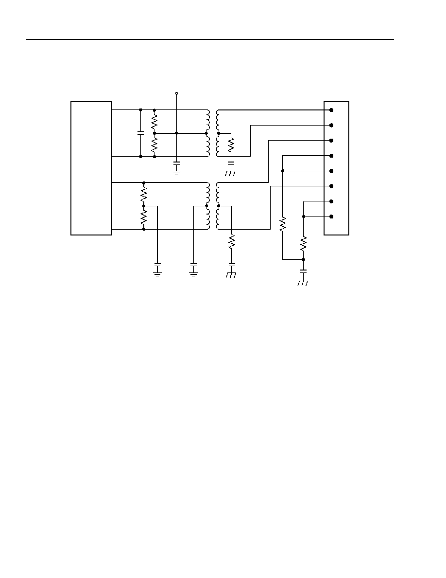
Figure 8. Typical Single-Channel Twisted-Pair (TP) Interface
DNC3X3625
RJ-45
1
2
3
4
5
6
7
8
75
75
0.01
µ
F
1:1
1:1
0.01
µ
F
0.01
µ
F
0.01
µ
F
TPI
TPIB
TPO
TPOB
50
50
V
DDO
75
0.01
µ
F
75
50
50
0.01
µ
F
10 pF

Advance Data Sheet
DNC3X3625
March 2000
10/100 Mbits/s Ethernet Transceiver Macrocell
19
4
Register Information
Register Descriptions
The MII management 16-bit register set implemented is as follows. The PHY address pins control the management
pins.
Table 12. Summary of Management Registers (MR)
Register
Address
Symbol
Name
Default
(Hex Code)
0
MR0
Control
3000h
1
MR1
Status
7849h
2
MR2
PHY Identifier 1
TBD
3
MR3
PHY Identifier 2
TBD
4
MR4
Autonegotiation Advertisement
01E1h
5
MR5
Autonegotiation Link Partner Ability
0000
6
MR6
Autonegotiation Expansion
0000
7
MR7
Next Page Transmit
0000
8--15
MR8--MR15
(Reserved)
--
16
MR16
PCS Control Register
0000
17
MR17
Autonegotiation (read register A)
0000
18
MR18
Autonegotiation (read register B)
0000
19
MR19
Lucent Analog Test Register
--
20
MR20
User-defined Register
--
21
MR21
RXER Counter
0000
22
MR22
Lucent Analog Test Registers
--
23
MR23
24
MR24
25
MR25
Lucent Analog Test (Tuner) Registers
--
26
MR26
27
MR27
28
MR28
Device Specific 1
--
29
MR29
Device Specific 2
2080
30
MR30
Device Specific 3
0000
31
MR31
Quick Status Register
--

20
DNC3X3625
Advance Data Sheet
10/100 Mbits/s Ethernet Transceiver Macrocell
March 2000
4
Register Information
(continued)
Table 13. MR0--Control Register Bit Descriptions
* The format for the bit descriptions is as follows: the first number is the register number, the second number is the bit position in the register.
R = read, W = write, NA = not applicable.
Bit*
Type
Description
0.15 (SW_RESET)
R/W
Reset. Setting this bit to a 1 will reset the DNC3X3625. All registers will be set
to their default state. This bit is self-clearing. The default is 0.
0.14 (LOOPBACK)
R/W
Loopback. When this bit is set to 1, no data transmission will take place on the
media. Any receive data will be ignored. The loopback signal path will contain
all circuitry up to, but not including, the PMD. The default value is a 0.
0.13 (SPEED100)
R/W
Speed Selection. The value of this bit reflects the current speed of operation
(1 = 100 Mbits/s; 0 = 10 Mbits/s). This bit will only affect operating speed when
the autonegotiation enable bit (register 0, bit 12) is disabled (0). This bit is
ignored when autonegotiation is enabled (register 0, bit 12). This bit is ANDed
with the SPEED_PIN signal.
0.12 (NWAY_ENA)
R/W
Autonegotiation Enable. The autonegotiation process will be enabled by set-
ting this bit to a 1. The default state is a 1.
0.11 (PWRDN)
R/W
Powerdown. The DNC3X3625 may be placed in a low-power state by setting
this bit to a 1, both the 10 Mbits/s transceiver and the 100 Mbits/s transceiver
will be powered down. While in the powerdown state, the DNC3X3625 will
respond to management transactions. The default state is a 0.
0.10 (ISOLATE)
R/W
Isolate. When this bit is set to a 1, the MII outputs will be brought to the high-
impedance state. The default state is a 0.
0.9 (REDONWAY)
R/W
Restart Autonegotiation. Normally, the autonegotiation process is started at
powerup. The process may be restarted by setting this bit to a 1. The default
state is a 0. The NWAYDONE bit (register 1, bit 5) is reset when this bit goes to
a 1. This bit is self-cleared when autonegotiation restarts.
0.8 (FULL_DUP)
R/W
Duplex Mode. This bit reflects the mode of operation (1 = full duplex; 0 = half
duplex). This bit is ignored when the autonegotiation enable bit (register 0,
bit 12) is enabled. The default state is a 0. This bit is ORed with the
F_DUP pin.
0.7 (COLTST)
R/W
Collision Test. When this bit is set to a 1, the DNC3X3625 will assert the
MCOL signal in response to MTX_EN.
0.6:0 (RESERVED)
NA
Reserved. All bits will read 0.

Advance Data Sheet
DNC3X3625
March 2000
10/100 Mbits/s Ethernet Transceiver Macrocell
21
4
Register Information
(continued)
Table 14. MR1--Status Register Bit Descriptions
* The format for the bit descriptions is as follows: the first number is the register number, the second number is the bit position in the register.
R = read.
Bit*
Type
Description
1.15 (T4ABLE)
R
100Base-T4 Ability. This bit will always be a 0.
0: Not able.
1: Able.
1.14 (TXFULDUP)
R
100Base-TX Full-Duplex Ability. This bit will always be a 1.
0: Not able.
1: Able.
1.13 (TXHAFDUP)
R
100Base-TX Half-Duplex Ability. This bit will always be a 1.
0: Not able.
1: Able.
1.12 (ENFULDUP)
R
10Base-T Full-Duplex Ability. This bit will always be a 1.
0: Not able.
1: Able.
1.11 (ENHAFDUP)
R
10Base-T Half-Duplex Ability. This bit will always be a 1.
0: Not able.
1: Able.
1.10:7 (RESERVED)
R
Reserved. All bits will read as a 0.
1.6 (NO_PA_OK)
R
Suppress Preamble. When this bit is set to a 1, it indicates that the
DNC3X3625 accepts management frames with the preamble suppressed.
1.5 (NWAYDONE)
R
Autonegotiation Complete. When this bit is a 1, it indicates the autonegotiation
process has been completed. The contents of registers MR4, MR5, MR6, and
MR7 are now valid. The default value is a 0. This bit is reset when autonegotia-
tion is started.
1.4 (REM_FLT)
R
Remote Fault. When this bit is a 1, it indicates a remote fault has been detected.
This bit will remain set until cleared by reading the register. The default is a 0.
1.3 (NWAYABLE)
R
Autonegotiation Ability. When this bit is a 1, it indicates the ability to perform
autonegotiation. The value of this bit is always a 1.
1.2 (LSTAT_OK)
R
Link Status. When this bit is a 1, it indicates a valid link has been established.
This bit has a latching function: a link failure will cause the bit to clear and stay
cleared until it has been read via the management interface.
1.1 (JABBER)
R
Jabber Detect. This bit will be a 1 whenever a jabber condition is detected. It will
remain set until it is read, and the jabber condition no longer exists.
1.0 (EXT_ABLE)
R
Extended Capability. This bit indicates that the DNC3X3625 supports the
extended register set (MR2 and beyond). It will always read a 1.

22
DNC3X3625
Advance Data Sheet
10/100 Mbits/s Ethernet Transceiver Macrocell
March 2000
4
Register Information
(continued)
Table 15. MR2, MR3--PHY Identification Registers (1 and 2) Bit Descriptions
* The format for the bit descriptions is as follows: the first number is the register number, the second number is the bit position in the register.
R = read.
Table 16. MR4--Autonegotiation Advertisement Register Bit Descriptions
* The format for the bit descriptions is as follows: the first number is the register number, the second number is the bit position in the register.
R = read, W = write.
Bit*
Type
Description
2.15:0 (OUI[3:18])
R
Organizationally Unique Identifier. The third through the twenty-fourth bit of the
OUI assigned to the PHY manufacturer by the
IEEE
are to be placed in bits
2.15:0 and 3.15:10. This value is programmable.
3.15:10 (OUI[19:24])
R
Organizationally Unique Identifier. The remaining 6 bits of the OUI. The value
for bits 24:19 is programmable.
3.9:4 (MODEL[5:0])
R
Model Number. 6-bit model number of the device. The model number is
programmable.
3.3:0 (VERSION[3:0])
R
Revision Number. The value of the present revision number. The version num-
ber is programmable.
Bit*
Type
Name/Description
4.15 (NEXT_PAGE)
R/W
Next Page. The next page function is activated by setting this bit to a 1. This will
allow the exchange of additional data. Data is carried by optional next pages of
information.
4.14 (ACK)
R/W
Acknowledge. This bit is the acknowledge bit from the link code word.
4.13 (REM_FAULT)
R/W
Remote Fault. When set to 1, the DNC3X3625 indicates to the link partner a
remote fault condition.
4.12:11
R/W
Reserved.
4.10 (PAUSE)
R/W
Pause. When set to a 1, it indicates that the DNC3X3625 wishes to exchange flow
control information with its link partner.
4.9 (100BASET4)
R/W
100Base-T4. This bit should always be set to 0.
4.8 (100BASET_FD)
R/W
100Base-TX Full Duplex. If written to 1, autonegotiation will advertise that the
DNC3X3625 is capable of 100Base-TX full-duplex operation.
4.7 (100BASETX)
R/W
100Base-TX. If written to 1, autonegotiation will advertise that the DNC3X3625 is
capable of 100Base-TX operation.
4.6 (10BASET_FD)
R/W
10Base-T Full Duplex. If written to 1, autonegotiation will advertise that the
DNC3X3625 is capable of 10Base-T full-duplex operation.
4.5 (10BASET)
R/W
10Base-T. If written to 1, autonegotiation will advertise that the DNC3X363x3625
is capable of 10Base-T operation.
4.4:0 (SELECT)
R/W
Selector Field. Reset with the value 00001 for
IEEE
802.3.

Advance Data Sheet
DNC3X3625
March 2000
10/100 Mbits/s Ethernet Transceiver Macrocell
23
4
Register Information
(continued)
Table 17. MR5--Autonegotiation Link Partner Ability (Base Page) Register Bit Descriptions
* The format for the bit descriptions is as follows: the first number is the register number, the second number is the bit position in the register.
R = read.
Table 18. MR5--Autonegotiation Link Partner (LP) Ability Register (Next Page) Bit Descriptions
* The format for the pin descriptions is as follows: the first number is the register number, the second number is the bit position in the register.
R = read.
Bit*
Type
Description
5.15 (LP_NEXT_PAGE)
R
Link Partner Next Page. When this bit is set to 1, it indicates that the link
partner wishes to engage in next page exchange.
5.14 (LP_ACK)
R
Link Partner Acknowledge. When this bit is set to 1, it indicates that the
link partner has successfully received at least three consecutive and consis-
tent FLP bursts.
5.13 (LP_REM_FAULT)
R
Remote Fault. When this bit is set to 1, it indicates that the link partner has
a fault.
5.12:5 (LP_TECH_ABILITY)
R
Technology Ability Field. This field contains the technology ability of the
link partner. These bits are similar to the bits defined for the MR4 register
(see Table 16).
5.4:0 (LP_SELECT)
R
Selector Field. This field contains the type of message sent by the link part-
ner. For
IEEE
802.3 compliant link partners, this field should read 00001.
Bit*
Type
Description
5.15 (LP_NEXT_PAGE)
R
Next Page. When this bit is set to a logic 0, it indicates that this is the last
page to be transmitted. A logic 1 indicates that additional pages will follow.
5.14 (LP_ACK)
R
Acknowledge. When this bit is set to a logic 1, it indicates that the link
partner has successfully received its partner's link code word.
5.13 (LP__MES_PAGE)
R
Message Page. This bit is used by the NEXT _PAGE function to differenti-
ate a message page (logic 1) from an unformatted page (logic 0).
5.12 (LP_ACK2)
R
Acknowledge 2. This bit is used by the NEXT_PAGE function to indicate
that a device has the ability to comply with the message (logic 1) or not
(logic 0).
5.11 (LP_TOGGLE)
R
Toggle. This bit is used by the arbitration function to ensure synchroniza-
tion with the link partner during next page exchange. Logic 0 indicates that
the previous value of the transmitted link code word was logic 1. Logic 1
indicates that the previous value of the transmitted link code word was
logic 0.
5.10:0 (MCF)
R
Message/Unformatted Code Field. With these 11 bits, there are 2048
possible messages. Message code field definitions are described in annex
28C of the
IEEE
802.3u standard.

24
DNC3X3625
Advance Data Sheet
10/100 Mbits/s Ethernet Transceiver Macrocell
March 2000
4
Register Information
(continued)
Table 19. MR6--Autonegotiation Expansion Register Bit Descriptions
* The format for the bit descriptions is as follows: the first number is the register number, the second number is the bit position in the register.
R = read, LH = latched high.
Bit*
Type
Description
6.15:5 (RESERVED)
R
Reserved.
6.4 (PAR_DET_FAULT)
R/LH Parallel Detection Fault. When this bit is set to 1, it indicates that a fault
has been detected in the parallel detection function. This fault is due to
more than one technology detecting concurrent link conditions. This bit
can only be cleared by reading this register.
6.3 (LP_NEXT_PAGE_ABLE)
R
Link Partner Next Page Able. When this bit is set to 1, it indicates that
the link partner supports the next page function.
6.2 (NEXT_PAGE_ABLE)
R
Next Page Able. This bit is set to 1, indicating that this device supports
the NEXT_PAGE function.
6.1 (PAGE_REC)
R/LH Page Received. When this bit is set to 1, it indicates that a NEXT_PAGE
has been received.
6.0 (LP_NWAY_ABLE)
R
Link Partner Autonegotiation Capable. When this bit is set to 1, it indi-
cates that the link partner is autonegotiation capable.

Advance Data Sheet
DNC3X3625
March 2000
10/100 Mbits/s Ethernet Transceiver Macrocell
25
4
Register Information
(continued)
Table 20. MR7--Next Page Transmit Register Bit Descriptions
* The format for the bit descriptions is as follows: the first number is the register number, the second number is the bit position in the register.
R = read, W = write.
Table 21. MR16--PCS Control Register Bit Descriptions
* The format for the bit descriptions is as follows: the first number is the register number, the second number is the bit position in the register.
R = read, W = write.
Bit*
Type
Description
7.15 (NEXT_PAGE)
R/W
Next Page. This bit indicates whether or not this is the last next page to be transmit-
ted. When this bit is 0, it indicates that this is the last page. When this bit is 1, it
indicates there is an additional next page.
7.14 (ACK)
R
Acknowledge. This bit is the acknowledge bit from the link code word.
7.13 (MESSAGE)
R/W
Message Page. This bit is used to differentiate a message page from an unformat-
ted page. When this bit is 0, it indicates an unformatted page. When this bit is 1, it
indicates a formatted page.
7.12 (ACK2)
R/W
Acknowledge 2. This bit is used by the next page function to indicate that a device
has the ability to comply with the message. It is set as follows:
s
When this bit is 0, it indicates the device cannot comply with the message.
s
When this bit is 1, it indicates the device will comply with the message.
7.11 (TOGGLE)
R
Toggle. This bit is used by the arbitration function to ensure synchronization with
the link partner during next page exchange. This bit will always take the opposite
value of the toggle bit in the previously exchanged link code word:
s
If the bit is a logic 0, the previous value of the transmitted link code word was a
logic 1.
s
If the bit is a 1, the previous value of the transmitted link code word was a 0.
The initial value of the toggle bit in the first next page transmitted is the inverse of
the value of bit 11 in the base link code word, and may assume a value of 1 or 0.
7.10:0 (MCF)
R/W
Message/Unformatted Code Field. With these 11 bits, there are 2048 possible
messages. Message code field definitions are described in annex 28C of the
IEEE
802.3u standard.
Bit*
Type
Description
16.15 (LOCKED)
R
Locked. Locked pin from descrambler block.
16.14-12 (Reserved)
R
Reserved. Should be written as 0.
16.11 (ANA_RG21)
R/W
Analog Regiser 21. Lucent Debug Register - Should be wrtten as 0.
16.10 (LPWR_TUN)
R/W
Low Power Tuner. Lucent Debug Register - Should be wrtten as 0.
16.9 (SMFIX_DA)
R/W
State Machine Fix. Lucent Debug Register - Should be written as 0.
16.8 (EN_NOWR)
R/W
Reserved. Should be written as 0.
16.7-6 (ATST1:0)
R/W
Autonegotiation Testmode (1:0). Lucent Debug Register - Should be written 0
16.5 (BYPPD125)
R/W
Bypass Powerdown 125. OR'd with BYPPD125 Input
16.4 (BYPPD160)
R/W
Bypass Powerdown 160. OR'd with BYPPD160 Input
16.3 (LOOPBACK)
R/W
Loopback Configure. When this bit is high, the entire loopback is performed in the
PCS macro. When this bit is low, only the collision pin is disabled in loopback.
16.2 (SCAN)
R/W
Scan Test Mode.
16.1 (FORCE
LOOPBACK)
R/W
Force Loopback. Force a loopback without forcing idle on the transmit side or dis-
abling the collision pin.
16.0 (SPEEDUP
COUNTERS)
R/W
Speedup Counters. Reduce link monitor counter to 10
µ
s from 620
µ
s. (Same as
FASTTEST = 1.)

26
DNC3X3625
Advance Data Sheet
10/100 Mbits/s Ethernet Transceiver Macrocell
March 2000
4
Register Information
(continued)
Table 22. MR17--Autonegotiation Read Register A
* The format for the bit descriptions is as follows: the first number is the register number, the second number is the bit position in the register.
R = read, W = write.
Table 23. MR18--Autonegotiation Read Register B
* The format for the bit descriptions is as follows: the first number is the register number, the second number is the bit position in the register.
R = read, W = write.
Bit*
Type
Description
17.15-13
R
Reserved. Always 0.
17.12
R
Next Page Wait.
17.11
R
Wait Link_Fail_Inhibit_Wait_Timer (Link Status Check).
17.10
R
Wait Autoneg_Wait_Timer (Link Status Check).
17.9
R
Wait Break_Link_Timer (Transmit Disable).
17.8
R
Parallel Detection Fault.
17.7
R
Autonegotiation Enable.
17.6
R
FLP Link Good Check.
17.5
R
Complete Acknowledge.
17.4
R
Acknowledge Detect.
17.3
R
FLP Link Good.
17.2
R
Link Status Check.
17.1
R
Ability Detect.
17.0
R
Transmit Disable.
Bit*
Type
Description
18.15
R
Receiving FLPs. Any of FLP Capture, Clock, Data_0, or Data_1 (FLP Rcv).
18.14
R
FLP Pass (FLP Rcv).
18.13
R
Link Pulse Count (FLP Rcv).
18.12
R
Link Pulse Detect (FLP Rcv).
18.11
R
Test Pass (NLP Rcv).
18.10
R
Test Fail Count (NLP Rcv).
18.9
R
Test Fail Extend (NLP Rcv).
18.8
R
Wait Max Timer Ack (NLP Rcv).
18.7
R
Detect Freeze (NLP Rcv).
18.6
R
Test Fail (NLP Rcv).
18.5
R
Transmit Count Ack (FLP Xmit).
18.4
R
Transmit Data Bit (FLP Xmit).
18.3
R
Transmit Clock Bit (FLP Xmit).
18.2
R
Transmit Ability (FLP Xmit).
18.1
R
Transmit Remaining Acknowledge (FLP Xmit).
18.0
R
Idle (FLP Xmit).

Advance Data Sheet
DNC3X3625
March 2000
10/100 Mbits/s Ethernet Transceiver Macrocell
27
4
Register Information
(continued)
Table 24. MR20--User-Defined Register
* The format for the bit descriptions is as follows: the first number is the register number, the second number is the bit position in the register.
R = read, W = write.
Table 25. MR21--RXER Counter
* The format for the bit descriptions is as follows: the first number is the register number, the second number is the bit position in the register.
R = read, W = write.
Table 26. MR28--Device-Specific Register 1 (Status Register) Bit Descriptions
Bit*
Type
Description
20.15:0
R/W
The data written into this user-defined register appears on the RG20_OUT[15:0]
bus.
Bit*
Type
Description
21.0
W
This bit, when 0 puts this register in 16-bit counter mode. When 1, it puts this regis-
ter in 8-bit counter mode. This bit is reset to a 0 and cannot be read.
21.15:0
R
When in 16-bit counter mode, these maintain a count of RXERs. It is reset on a read
operation.
21.7:0
R
When in 8-bit counter mode, these maintain a count of RXERs. It is reset on a read
operation.
21.11:8
R
When in 8-bit mode, these contain a count of false carrier events (802.3 Section
27.3.1.5.1). It is reset on a read operaton.
21.15:12
R
When in 8-bit mode, these contain a count of disconnect events (Link Unstable 6,
802.3 Section 27.3.1.5.1). It is reset on a read operation.
Bit*
Type
Description
28.15:9 (UNUSED)
R
Unused. Read as 0.
28.8 (BAD_FRM)
R/LH
Bad Frame. If this bit is a 1, it indicates a packet has been received without an
SFD. This bit is only valid in 10 Mbits/s mode.
This bit is latching high and will only clear after it has been read or the device has
been reset.
28.7 (CODE)
R/LH
Code Violation. When this bit is a 1, it indicates a Manchester code violation has
occurred. The error code will be output on the MRXD lines. Refer to Table 1 for a
detailed description of the MRXD pin error codes. This bit is only valid in
10 Mbits/s mode.
This bit is latching high and will only clear after it has been read or the device has
been reset.
28.6 (APS)
R
Autopolarity Status. When register 30, bit 3 is set and this bit is a 1, it indicates
the DNC3X3625 has detected and corrected a polarity reversal on the twisted pair.
If the APF_EN bit (register 30, bit 3) is set, the reversal will be corrected inside the
DNC3X3625. This bit is not valid in 100 Mbits/s operation.
28.5 (DISCON)
R/LH
Disconnect. If this bit is a 1, it indicates a disconnect. This bit will latch high until
read. This bit is only valid in 100 Mbits/s mode.
28.4 (UNLOCKED)
R/LH
Unlocked. Indicates that the TX scrambler lost lock. This bit will latch high until
read. This bit is only valid in 100 Mbits/s mode.
28.3 (RXERR_ST)
R/LH
RX Error Status. Indicates a false carrier. This bit will latch high until read. This bit
is only valid in 100 Mbits/s mode.
28.2 (FRC_JAM)
R/LH
Force Jam. This bit will latch high until read. This bit is only valid in 100 Mbits/s
mode.

28
DNC3X3625
Advance Data Sheet
10/100 Mbits/s Ethernet Transceiver Macrocell
March 2000
4
* The format for the bit descriptions is as follows: the first number is the register number, the second number is the bit position in the register.
R = read, LH = latched high.
Table 27. MR29--Device-Specific Register 2 (100 Mbits/s Control) Bit Descriptions
Bit*
Type
Description
28.1 (LNK100UP)
R
Link Up 100. This bit, when set to a 1, indicates a 100 Mbits/s transceiver is up
and operational.
28.0 (LNK10UP)
R
Link Up 10. This bit, when set to a 1, indicates a 10 Mbits/s transceiver is up and
operational.
Bit*
Type
Description
29.15 (LOCALRST)
R/W
Management Reset. This is the local management reset bit. Writing a logic 1 to
this bit will cause the lower 16 registers and registers 28 and 29 to be reset to
their default values. This bit is self-clearing.
29.14 (RST1)
R/W
Generic Reset 1. This register is used for manufacture test only.
29.13 (RST2)
R/W
Generic Reset 2. This register is used for manufacture test only.
29.12 (100_OFF)
R/W
100 Mbits/s Transmitter Off. When this bit is set to 0, it forces TPI low and
TPIB high. This bit defaults to 1.
29.11 (LED_BLINK
R/W
LED Blinking. This register, when 1, enables LED blinking. This is ORed with
LED_BLINK_EN. Default is 0.
29.10 (CRS_SEL)
R/W
Carrier Sense Select. MCRS will be asserted on receive only when this bit is
set to a 1. If this bit is set to logic 0, MCRS will by asserted on receive or trans-
mit. This bit is ORed with the CRS_SEL pin.
29.9 (LINK_ERR)
R/W
Link Error Indication. When this bit is a 1, a link error code will be reported on
MRXD[3:0] of the DNC3X3625 when MRX_ER is asserted on the MII. The spe-
cific error codes are listed in the MRXD pin description. If it is 0, it will disable this
function.
29.8 (PKT_ERR)
R/W
Packet Error Indication Enable. When this bit is a 1, a packet error code,
which indicates that the scrambler is not locked, will be reported on MRXD[3:0]
of the DNC3X3625 when MRX_ER is asserted on the MII. When this bit is 0, it
will disable this function.
29.7 (PULSE_STR)
R/W
Pulse Stretching. When this bit is set to 1, the CS, XS, and RS output signals
will be stretched between approximately 42 ms--84 ms. If this bit is 0, it will dis-
able this feature. Default state is 0.
29.6 (EDB)
R/W
Encoder/Decoder Bypass. When this bit is set to 1, the 4B/5B encoder and
5B/4B decoder function will be disabled. This bit is ORed with the EDBT pin.
29.5 (SAB)
R/W
Symbol Aligner Bypass. When this bit is set to 1, the aligner function will be
disabled.
29.4 (SDB)
R/W
Scrambler/Descrambler Bypass. When this bit is set to 1, the scrambling/
descrambling functions will be disabled. This bit is ORed with the SDBT pin.
29.3 (CARIN_EN)
R/W
Carrier Integrity Enable. When this bit is set to a 1, carrier integrity is enabled.
This bit is ORed with the CARIN_EN pin.
29.2 (JAM_COL)
R/W
Jam Enable. When this bit is a 1, it enables JAM associated with carrier integrity
to be ORed with MCOLMCRS.
Register Information
(continued)
Table 26. MR28--Device-Specific Register 1 (Status Register) Bit Descriptions (continued)
* The format for the bit descriptions is as follows: the first number is the register number, the second number is the bit position in the register.
R = read, W = write.

Advance Data Sheet
DNC3X3625
March 2000
10/100 Mbits/s Ethernet Transceiver Macrocell
29
4
* The format for the bit descriptions is as follows: the first number is the register number, the second number is the bit position in the register.
R = read, W = write.
Table 28. MR30--Device-Specific Register 3 (10 Mbits/s Control) Bit Descriptions
* The format for the bit descriptions is as follows: the first number is the register number, the second number is the bit position in the register.
R = read, W = write.
Bit*
Type
Description
29.1 (FEF_EN)
R/W
Far-End Fault Enable. This bit is used to enable the far-end fault detection and
transmission capability. This capability may only be used if autonegotiation is
disabled. This capability is to be used only with media which does not support
autonegotiation. Setting this bit to 1 enables far-end fault detection, and logic 0
will disable the function. Default state is 0.
29.0 (FX)
R/W
Fiber-Optic Mode. When this bit is a 1, the DNC3X3625 is in fiber-optic mode.
This bit is ORed with FX_MODE.
Bit*
Type
Description
30.15 (Test10TX)
R/W
When high and 10Base-T is powered up, a continuous 10 MHz signal (1111)
will be transmitted. This is only meant for testing. Default is 0.
30.14 (RxPLLEn)
R/W
When high, all 10Base-T logic will be powered up when the link is up. Other-
wise, portions of the logic will be powered down when no data is being
received to conserve power. Default is 0.
30.13 (JAB_DIS)
R/W
Jabber Disable. When this bit is 1, disables the jabber function of the
10Base-T receive. Default is 0.
30.12:7 (Reserved)
R/W
Reserved. Should be written as 0.
30.6 (LITF_ENH)
R/W
Enhanced Link Integrity Test Function. When high, function is enabled.
This is ORed with the LITF_ENH input. Default is 0.
30.5 (HBT_EN)
R/W
Heartbeat Enable. When this bit is a 1, the heartbeat function will be enabled.
Valid in 10 Mbits/s mode only.
30.4 (ELL_EN)
R/W
Extended Line Length Enable. When this bit is a 1, the receive squelch lev-
els are reduced from a nominal 435 mV to 350 mV, allowing reception of sig-
nals with a lower amplitude. Valid in 10 Mbits/s mode only.
30.3 (APF_EN)
R/W
Autopolarity Function Disable. When this bit is a 0 and the DNC3X3625 is
in 10 Mbits/s mode, the autopolarity function will determine if the TP link is
wired with a polarity reversal.
If there is a polarity reversal, the DNC3X3625 will assert the APS bit (register
28, bit 6) and correct the polarity reversal. If this bit is a 1 and the device is in
10 Mbits/s mode, the reversal will not be corrected.
30.2 (RESERVED)
R/W
Reserved. Should be written as 0.
30.1 (SERIAL _SEL)
R/W
Serial Select. When this bit is set to a 1, 10 Mbits/s serial mode will be
selected. When the DNC3X3625 is in 100 Mbits/s mode, this bit will be
ignored.
30.0 (ENA_NO_LP)
R/W
No Link Pulse Mode. Setting this bit to a 1 will allow 10 Mbits/s operation
with link pulses disabled. If the DNC3X3625 is configured for 100 Mbits/s
operation, setting this bit will not affect operation.
Register Information
(continued)
Table 27. MR29--Device-Specific Register 2 (100 Mbits/s Control) Bit Descriptions (continued)

30
DNC3X3625
Advance Data Sheet
10/100 Mbits/s Ethernet Transceiver Macrocell
March 2000
4
Register Information
(continued)
Table 29. MR31--Device-Specific Register 4 (Quick Status) Bit Descriptions
* The format for the bit descriptions is as follows: the first number is the register number, the second number is the bit position in the register.
R = read, W = write.
Register/Bit
*
Type
Description
31.15 (ERROR)
R
Receiver Error. When this bit is a 1, it indicates that a receive error has been
detected. This bit is valid in 100 Mbits/s only. This bit will remain set until cleared by
reading the register. Default is a 0.
31.14 (RXERR_ST)/
(LINK_STAT_CHANGE)
R
False Carrier. When bit [31.7] is set to 0 and this bit is a 1, it indicates that the carrier
detect state machine has found a false carrier. This bit is valid in 100 Mbits/s only. This
bit will remain set until cleared by reading the register. Default is 0.
Link Status Change. When bit [31.7] is set to a 1, this bit is redefined to become the
LINK_STAT_CHANGE bit and goes high whenever there is a change in link status (bit
[31.11] changes state).
31.13 (REM_FLT)
R
Remote Fault. When this bit is a 1, it indicates a remote fault has been detected. This
bit will remain set until cleared by reading the register. Default is a 0.
31.12 (UNLOCKED)/
(JABBER)
R
Unlocked/Jabber. If this bit is set when operating in 100 Mbits/s mode, it indicates
that the TX descrambler has lost lock. If this bit is set when operating in 10 Mbits/s
mode, it indicates a jabber condition has been detected. This bit will remain set until
cleared by reading the register.
31.11 (LSTAT_OK)
R
Link Status. When this bit is a 1, it indicates a valid link has been established. This bit
has a latching low function: a link failure will cause the bit to clear and stay cleared
until it has been read via the management interface.
31.10 (PAUSE)
R
Link Partner Pause. When this bit is set to a 1, it indicates that the DNC3X3625
wishes to exchange flow control information.
31.9 (SPEED100)
R
Link Speed. When this bit is set to a 1, it indicates that the link has negotiated to
100 Mbits/s. When this bit is a 0, it indicates that the link is operating at 10 Mbits/s.
31.8 (FULL_DUP)
R
Duplex Mode. When this bit is set to a 1, it indicates that the link has negotiated to
full-duplex mode. When this bit is a 0, it indicates that the link has negotiated to half-
duplex mode.
31.7 (INT_CONF)
R/W
Interrupt Configuration. When this bit is set to a 0, it defines bit [31.14] to be the
RXERR_ST bit and the interrupt pin (MASK_STAT_INT) goes high whenever any of
bits [31.15:12] go high, or bit [31.11] goes low. When this bit is set high, it redefines
bit [31.14] to become the LINK_STAT_CHANGE bit, and the interrupt pin
(MASK_STAT_INT) goes high only when the link status changes (bit [31.14] goes
high). This bit defaults to 0.
31.6 (INT_MASK)
R/W
Interrupt Mask. When set high, no interrupt is generated by this channel under any
condition. When set low, interrupts are generated according to bit [31.7].
31.5:3
(LOW_AUTO__STATE)
R
Lowest Autonegotiation State. These 3 bits report the state of the lowest autonego-
tiation state reached since the last register read, in the priority order defined below:
000: Autonegotiation enable.
001: Transmit disable or ability detect.
010: Link status check.
011: Acknowledge detect.
100: Complete acknowledge.
101: FLP link good check.
110: Next page wait.
111: FLP link good.
31.2:0
(HI_AUTO_STATE)
R
Highest Autonegotiation State. These 3 bits report the state of the highest autone-
gotiation state reached since the last register read, as defined above for bit [31.5:3].

Advance Data Sheet
DNC3X3625
March 2000
10/100 Mbits/s Ethernet Transceiver Macrocell
31
4
Application Notes: Board Layout
Board Layout Considerations
In order to obtain optimum performance, careful atten-
tion must be paid to the circuit board layout, shielding,
and the placement of components. Careful routing of
high-speed lines is mandatory. Power supply input pins
must be protected from noisy conditions by proper fil-
tering. To achieve these design goals, the following
steps are recommended as a minimum.
1. As a minimum, a four-layer circuit board, with two-
ounce copper planes, should be used. This will mini-
mize the switching transients by providing a low-
impedance power source. The signal planes should
be isolated from each other by the power and/or
ground planes. Do not segment the ground plane
except around the RJ-45 connectors and magnetics
module as described below. Use a single, continu-
ous plane. The reference design will be a six-layer
board.
2. Power and ground planes should extend underneath
the ASIC up to the input of the magnetic module.
Power and ground planes should not extend under
any network signal path, or the magnetics module,
because common-mode power supply noise will be
coupled to the signals. The greater the distance
between the planes and the network signals, the
lower the EMI emissions. Chassis ground may be
used under the RJ-45 connectors if desired.
3. The power plane of the ASIC should be separated
into three regions: digital power (V
DDD;
this is the
PWB's V
DD
plane), analog power (V
DDA
), and output
driver power (V
DDO
). For conservative designs, the
V
DDA
segment and the V
DDO
segment, should be fil-
tered with a ferrite bead, 10
µ
F, and 0.01
µ
F capaci-
tors before connecting to the V
DD
plane with a heavy
wide trace. Pins 80 V
DDPLL
and 83 V
DDPD
can be
connected together and filtered with a ferrite bead
and 10
µ
F and 0.01
µ
F capacitors for conservative
designs. Refer to Figure 3 for suggested layout. Do
not overlay different power planes on different layers,
unless they are separated by a ground plane. When
segmenting power planes on the same layer they
should be separated by at least three times the dis-
tance to the nearest ground layer.
4. The liberal use of capacitors on each the power pins
of the ASIC will minimize any noise coupled into the
power plane. Power supply noise contributes to the
EMI emissions in circuit layouts. Low ESR capacitors
between the power and ground planes must be
placed as close as possible to all the DNC3X3625
power pins. Low-inductance short connections to
each power pin and the ground plane are required.
This can be achieved by using short traces to the
power pins and connecting to the ground plane with
two vias. Multilayer ceramic capacitors with good
quality dielectric such as NPO or X7R (avoid using
Z5U) are recommended for the low ESR capacitors.
A 0.01
µ
F capacitor should be used on every pin, for
conservative designs two capacitors can be used on
every pin a 0.1
µ
F and a 0.001
µ
F.
5. Route the transmit and receive pairs between the
ASIC, the magnetics, and the RJ-45 connectors as
short, straight, and equal length as possible. These
traces should be routed with 50
impedance to the
nearest power/ground plane with a differential
impedance of 100
. Keep the separation between
adjacent pairs on the same layer, 2 mm or more if
possible to minimize crosstalk.
6. The most EMI critical routing is between the mag-
netic module (after common-mode filters) and the
RJ-45 connectors. Use the chassis of the system to
allow coupled noise to flow to ground via common
mode terminations. The chassis is not a perfect
ground, but with proper power supply design, the
chassis can be used to redirect some common-
mode noise.
7. Reduce the number of vias on the transmit path.
Vias can have resonance at critical frequencies
degrading EMI emissions performance. The transmit
differential pairs from the RJ-45 to the magnetics
and the DNC3X3625 can be run on the top layer of
the board. Vias on the receive path should be mini-
mized but are less critical because the signal energy
is less than on the transmit path. The receive signals
can be run on a buried layer or on the bottom layer.
8. Ensure that the 25 MHz crystal and the load capaci-
tors (33 pF), or the oscillator (25 MHz, 50 MHz, or
125 MHz, if used), are located as close to the XLO/
XHI pins as possible. All bias resistors (pins 13, 25,
42, and 43) and reference capacitor (pin 81) must be
located within close proximity to the PHY. This will
reduce the coupled noise into the bias circuits. Place
receive twisted-pair terminating resistors (100
) as
close to PHY pins as possible.
9. Never route clock or high-speed signal lines under
the ASIC unless the lines are under a ground or
power plane.

4
Lucent Technologies Inc. reserves the right to make changes to the product(s) or information contained herein without notice. No liability is assumed as a result of their use or application. No
rights under any patent accompany the sale of any such product(s) or information.
Copyright © 2000 Lucent Technologies Inc.
All Rights Reserved
March 2000
DS00-078LAN
For additional information, contact your Microelectronics Group Account Manager or the following:
INTERNET:
http://www.lucent.com/micro
E-MAIL:
docmaster@micro.lucent.com
N. AMERICA:
Microelectronics Group, Lucent Technologies Inc., 555 Union Boulevard, Room 30L-15P-BA, Allentown, PA 18103
1-800-372-2447, FAX 610-712-4106 (In CANADA: 1-800-553-2448, FAX 610-712-4106)
ASIA PACIFIC: Microelectronics Group, Lucent Technologies Singapore Pte. Ltd., 77 Science Park Drive, #03-18 Cintech III, Singapore 118256
Tel. (65) 778 8833, FAX (65) 777 7495
CHINA:
Microelectronics Group, Lucent Technologies (China) Co., Ltd., A-F2, 23/F, Zao Fong Universe Building, 1800 Zhong Shan Xi Road, Shanghai
200233 P. R. China Tel. (86) 21 6440 0468, ext. 316, FAX (86) 21 6440 0652
JAPAN:
Microelectronics Group, Lucent Technologies Japan Ltd., 7-18, Higashi-Gotanda 2-chome, Shinagawa-ku, Tokyo 141, Japan
Tel. (81) 3 5421 1600, FAX (81) 3 5421 1700
EUROPE:
Data Requests: MICROELECTRONICS GROUP DATALINE: Tel. (44) 7000 582 368, FAX (44) 1189 328 148
Technical Inquiries: GERMANY: (49) 89 95086 0 (Munich), UNITED KINGDOM: (44) 1344 865 900 (Ascot),
FRANCE: (33) 1 40 83 68 00 (Paris), SWEDEN: (46) 8 594 607 00 (Stockholm), FINLAND: (358) 9 4354 2800 (Helsinki),
ITALY: (39) 02 6608131 (Milan), SPAIN: (34) 1 807 1441 (Madrid)