 | –≠–ª–µ–∫—Ç—Ä–æ–Ω–Ω—ã–π –∫–æ–º–ø–æ–Ω–µ–Ω—Ç: DNCX01 | –°–∫–∞—á–∞—Ç—å:  PDF PDF  ZIP ZIP |

Advance Data Sheet
September 1997
Features
s
Compatible with
IEEE*
802.3 10Base-T
standards for twisted-pair (TP) cable
s
Digital phase-locked loop (DPLL) timing recovery
and data decoding
s
On-chip filtering eliminates the need for external
filters
s
Encodes NRZ data to Manchester data and sup-
plies the associated predistortion signals needed
for TP transmission
s
Generates IDL pulse at end-of-transmit packet
s
Detects collisions and Manchester code violations
s
Interfaces with
IEEE
802.3u standard MII interface
or a serial 10 Mbits/s interface
s
Full-duplex capability
s
Autopolarity sensing and correction
s
Powerdown mode
s
Adjustable squelch level for extended wire length
capability (two levels)
s
Six status signals: receive, transmit, collision, jab-
ber, link integrity, and polarity fault
s
Supports MII management interface
s
Supported in Lucent Technologies Microelectronics
Groups' submicron high-speed HS350C and
HS350CDE 0.35
µ
m 5 V CMOS standard-cell
libraries
*
IEEE
is a registered trademark of The Institute of Electrical and
Electronics Engineers, Inc.
Description
Lucent Technologies' DNCX01 macrocell integrates
the physical layer function of the 802.3 10Base-T TP
interface and provides the following functions:
s
Timing recovery
s
Encoding/decoding for data conversion
s
Local loopback (LLB)
s
Autopolarity sensing and correction
s
Remote fault signaling
s
Link integrity
s
Jabber
s
Signal quality error (SQE) function
s
Data predistortion
s
Powerdown mode
In addition, the DNCX01 provides an internal testing
MUX that is used to isolate the DNCX01 from the
ASIC controller to facilitate production testing that uti-
lizes Lucent Technologies' comprehensive mixed-
signal test program.
The DNCX01's TP drivers may be used as a macro
when used with other 10Base-T LAN ASIC applica-
tions.
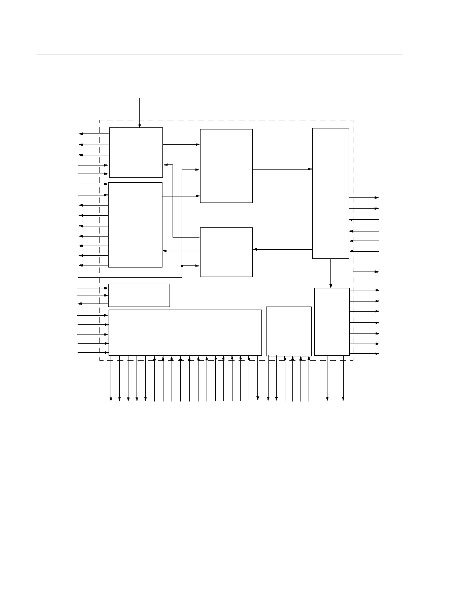
Figure 1 shows a functional block diagram of the
DNCX01 macrocell.
DNCX01
10Base-T Physical Interface ASIC Macrocell
Note: Advisories are issued as needed to update product information. When using this data sheet for design purposes, please contact
your Lucent Technologies Microelectronics Group Account Manager to obtain the latest advisory on this product.
DNCX01
Advance Data Sheet
10Base-T Physical Interface ASIC Macrocell
September 1997
2
Lucent Technologies Inc.
Description
(continued)
5-5966(F).r1
Figure 1. Functional Block Diagram
STXC
STEN
STXD
MTXD[3:0]
MTX_EN
MTXCLK
MCOL
MRXD[3:0]
MRXCLK
MII
INTERFACE
ENCODER
TP
TPB
DI
DIN
REFR
REFR2
DECODER
TPRS
TPXS
TPCS
TPJS
TPLIS
TPAPS
TP
INTERFACE
STATUS
SIGNALS
CLK20
TEST
RDB
US[15:0]
RREG28
RREG30C
COL_TST
RESET
F_DUP
ISOLA
TE
LPBK
MNG_CLK
MNG_REST
OUT[20:0]
SRXC
SRXD
SERIAL
INTERFACE
APFE_PIN
SERIAL_SEL
PHY_SEL
WRBUS[15:0]
PWRDN
MANAGEMENT INTERFACE
CRS_SEL
MRX_DV
MCRS
REF_10
HBT_PIN
NOLP_PIN
REF_SEL_PIN
SER_SEL_PIN
SER_SEL
ELLE_PIN
IN[21:0]
BOUT[20:0]
TEST1
TEST0
BIN[21:0]
LINK_LED
CD
VIOL
AUTONEGOTIATION
SLIP
SMT_SQ
AUTO_EN
MRX_ER
WREG30
BAD_FR
BUF20

Advance Data Sheet
DNCX01
September 1997
10Base-T Physical Interface ASIC Macrocell
Lucent Technologies Inc.
3
I/O Information
I/O Descriptions
Table 1. MII Interface
1. Y = yes. This signal is repeated four times.
2. X = don't care.
Signal/Duplicate
1
Type
Name/Description
Test
Mode
2
MTXD[3:0]
Y
I
Transmit Data.
4-bit parallel data input synchronous with MTXCLK.
X
MTX_EN
Y
I
Transmit Enable.
A logic high on this signal indicates that there is data on
MTXD[3:0]. This signal also starts the jabber timer. MTX_EN is synchro-
nous with MTXCLK.
X
MCOL
Y
O
Collision Detect
. This signal signifies that a collision has occurred on the
network or that a heartbeat signal has been received. When SERIAL_SEL
is high, this signal will also indicate that the jabber timer has expired.
X
MCRS
Y
O
Carrier Sense
. This signal is asserted when either the transmit or receive
medium is nonidle. This signal remains asserted throughout a collision con-
dition.
X
MRXCLK
Y
O
Receive Clock.
2.5 MHz clock that provides the timing reference for the
transfer of MRX_DV and MRXD signals from the DNCX01. MRXCLK is
always active but will switch to the transmit clock when no data is being
received.
X
MRXD[3:0]
Y
O
Receive Data.
4-bit parallel data outputs that are synchronous to
MRXCLK.
X
MRX_DV
Y
O
Receive Data Valid.
This signal
indicates that the DNCX01 is recovering
and decoding nibbles on MRXD[3:0] and that the data is synchronous with
MRXCLK.
X
MTXCLK
Y
O
Transmit Clock.
2.5 MHz clock that provides timing reference for the trans-
fer of the MTX_EN and MTXD signals.
X
MRX_ER
Y
O
Receiver Error.
This signal indicates that the DNCX01 has detected a cod-
ing error in the frame presently being transferred. MRX_ER is synchronous
with MRXCLK. (This signal is not required by the
IEEE
802.3 standard and
is optional.)
X

DNCX01
Advance Data Sheet
10Base-T Physical Interface ASIC Macrocell
September 1997
4
Lucent Technologies Inc.
I/O Information
(continued)
I/O Descriptions
(continued)
Table 2. Serial 10 Mbits/s Interface
1. Y = yes. This signal is repeated four times. N = no. This signal is not repeated.
2. X = don't care.
Signal/Duplicate
1
Type
Name/Description
Test
Mode
2
SRXC
Y
O
Receive Clock
. This signal is the recovered clock derived from the
received Manchester data and has a nominal period of 100 ns. SRXC
will remain active for at least 4 clock cycles after a packet is received.
This signal is only used when using a 10 Mbits/s serial interface
instead of the 2.5 Mbits/s MII interface.
X
SRXD
Y
O
Receive Data
. This signal is the NRZ data that represents the
decoded Manchester data from the TP media. This signal is only used
when using a 10 Mbits/s serial interface instead of the 2.5 Mbits/s MII
interface.
X
STXC
Y
O
Transmit Clock.
This signal is a 10 MHz clock output for use by the
controller. This signal is only used when using a 10 Mbits/s serial inter-
face instead of the 2.5 Mbits/s MII interface.
X
STEN
Y
I
Transmit Enable.
A logic high on this signal indicates that the data on
STXD is valid, and begins transmission on the TP media. This signal
also starts the jabber timer. This signal is only used when using a
10 Mbits/s serial interface instead of the 2.5 Mbits/s MII interface.
X
STXD
Y
I
Transmit Data.
This signal must be driven with the serial NRZ data to
be put onto the TP media. This signal is only used when using a
10 Mbits/s serial interface instead of the 2.5 Mbits/s MII interface.
X
REF_10
N
I
10 MHz Reference Clock.
This reference is only used when the
REF_SEL control pin is set. This clock needs to be phase-locked with
CLK20.
X

Lucent Technologies Inc.
5
Advance Data Sheet
DNCX01
September 1997
10Base-T Physical Interface ASIC Macrocell
I/O Information
(continued)
I/O Descriptions
(continued)
Table 3.Twisted-Pair (TP) Interface
1. Y = yes. This signal is repeated four times.
2. A = analog signal.
3. C = needs to be controlled; O = observed.
Table 4. Control
1. Y = yes. This signal is repeated four times.
2. X = don't care.
Signal/Duplicate
1
Type
2
Name/Description
Test
Mode
3
DI
Y
I (A)
Twisted-Pair Receive Data
. This differential input, connected to the TP
media.
C
DIN
Y
I (A)
Twisted-Pair Receive Data
. This signal is the inverse of TPI.
C
TP
Y
O (A)
Twisted-Pair Transmit Data
. This differential current drive signal con-
tains all filtering necessary to connect to the TP media. The signal is the
Manchester-encoded data derived from the NRZ data presented to the
MTXD input, including the required IDL pulse at the end of the packet.
O
TPB
Y
O (A)
Twisted-Pair Transmit Data
. This signal is the inverse of TPO.
O
Signal/Duplicate
1
Type
Name/Description
Test
Mode
2
COL_TST
Y
I
Collision Test.
When this input is high, the DNCX01 will assert the
MCOL signal within 512 BT in response to the assertion of MTX_EN.
While COL_TST is high, the DNCX01 will deassert the MCOL signal
within 4 BT of MTX_EN being deasserted. A logic low on the
COL_TST input will allow normal operation.
X
CRS_SEL
Y
I
Carrier Sense Select.
When this input is high, CRS will be asserted
on receive only. When low, CRS will be asserted on receive and trans-
mit.
X
F_DUP
Y
I
Full Duplex.
When this input is high, it configures the DNCX01 for full-
duplex operation; when low, the DNCX01 is configured for half-duplex
operation.
X
ISOLATE
Y
I
Isolate.
When this input is high, the DNCX01 will drive MCOL and
MCRS low. MTXD[3:0] and MTX_EN will be ignored. For the serial
interface, the DNCX01 will drive SRXC, SRXD, and STXC low and
ignore STEN and STXD. While isolated, the DNCX01 will respond to
management transactions.
X
LPBK
Y
I
Loopback.
A high on this input will place the DNCX01 into loopback
mode; a low will place the DNCX01 into normal operation.
X
PHY_SEL
Y
I
PHY Select.
A logic high on this input indicates to the DNCX01 that
the management block has selected the DNCX01 to be the active
PHY.
X
PWRDN
Y
I
Powerdown Mode.
A
high on this input will place the DNCX01 into
powerdown mode. The powerdown mode will shut down all dynamic
logic. This input must be low or reset must be asserted for 1.0 ms to
bring the DNCX01 out of the powerdown mode.
X

DNCX01
Advance Data Sheet
10Base-T Physical Interface ASIC Macrocell
September 1997
6
Lucent Technologies Inc.
I/O Information
(continued)
I/O Descriptions
(continued)
Table 5. Autonegotiation Pins
1. Y = yes. This signal is repeated four times.
2. X = don't care; C = needs to be controlled.
Table 6. Status
1. Y = yes. This signal is repeated four times.
2. X = don't care.
Signal/Duplicate
1
Type
Name/Description
Test
Mode
2
AUTO_EN
Y
I
Autonegotiation Enable.
When this input is high, the DNCX01 will be
enabled to be used by the autonegotiation state machine.
C
SLIP
Y
I
Send Link Pulse.
When AUTO_EN is 1, the autonegotiation block will
send a pulse that in turn causes the DNCX01 to transmit a link pulse.
When AUTO_EN is 0, this input is ignored.
C
SMT_SQ
Y
O
Found Energy.
This signal indicates that the DNCX01 has detected
energy for more than 25 ns.
X
Signal/Duplicate
1
Type
Name/Description
Test
Mode
2
LINK_LED
Y
O
Link LED.
This pin is high whenever the link is up. This signal can
go to a register or an LED driver.
X
TPAPS
Y
O
TP Autopolarity Status
. This signal will indicate that the embedded
MAU has determined that the TP link has been wired with a polarity
reversal and the APFE input is logic high. A polarity correction will
only occur if the APFE input is logic high. This signal can go to a
register or an LED driver.
X
TPCS
Y
O
TP Collision Status
. This signal will indicate a collision has
occurred on the TP media. This signal can go to a register or an
LED driver.
X
TPJS
Y
O
TP Jabber Status
. This signal will indicate when a jabbed MAU
condition has occurred on the TP media. This signal can go to a reg-
ister or an LED driver.
X
TPLIS
Y
O
TP Link-Integrity Status
. This signal will indicate when the embed-
ded MAU has determined the TP link to be present. This signal can
go to a register or an LED driver. Also, this pin is high when in pow-
erdown or PHY_SEL = 0.
X
TPRS
Y
O
TP Receive Status
. This signal will indicate when a packet is
received from the TP media. This signal can go to a register or an
LED driver.
X
TPXS
Y
O
TP Transmit Status
. This signal will indicate when a packet is trans-
mitted onto the TP media. This signal can go to a register or an LED
driver. Once set, this will remain high until RREG28 goes high.
X
BAD_FR
Y
O
Bad Frame Received.
This output indicates valid Manchester data
was received without a start of frame delimiter (SFD). Once set, this
will remain high until RREG28 goes high.
X
CDVIOL
Y
O
Code Violation Output.
This output indicates Manchester code vio-
lation has occurred. Once set, this will remain high until RREG28
goes high.
X

Advance Data Sheet
DNCX01
September 1997
10Base-T Physical Interface ASIC Macrocell
Lucent Technologies Inc.
7
I/O Information
(continued)
I/O Descriptions
(continued)
Table 7. Miscellaneous
1. Y = yes. This signal is repeated four times. N = no. This signal is not repeated.
2. A = analog signal.
3. X = don't care; C = needs to be controlled.
Signal/Duplicate
1
Type
2
Name/Description
Test
Mode
3
RESET
Y
I
Reset. When this signal is high, the DNCX01 will reset. This signal
should be asserted for 1.0 ms after power is initially applied or after
being released from powerdown mode.
X
CLK20
N
I (A)
20.0 MHz Clock. This input accepts a 20 MHz clock (
±
100 ppm),
45%--55% duty cycle.
C
BUF20
N
O
Buffered 20 MHz Clock. This buffered version of the 20 MHz clock
runs whenever DNCX01 PHY_SEL is high and PWRDN is low.
X
REFR
N
I/O (A)
Reference Resistor. Connect this pin to ground through a 24.9 k
resistor to provide a reference for the bias current.
C
REFR2
N
I/O (A)
Reference Resistor. Connect this pin to ground through a 24.9 k
resistor to provide a reference for the bias current.
C

DNCX01
Advance Data Sheet
10Base-T Physical Interface ASIC Macrocell
September 1997
8
Lucent Technologies Inc.
I/O Information
(continued)
I/O Descriptions
(continued)
Table 8. Management Register
1. Y = yes. This signal is repeated four times.
2. X = don't care.
Signal/Duplicate
1
Type
Name/Description
Test
Mode
2
WRBUS[15:0]
Y
I
Management Write Bus. This 16-bit bus is used by the management block
to write the management register located inside of DNCX01. The data is
stored in the management register when the WR pin is active. When WR
pin is inactive, the management register holds its current value. The bits are
defined as follows:
15 = Disable common mode (test only).
14 = Enable frequency synthesizer (test only).
13:6 = Unused.
5 = Heartbeat Enable (HBT_EN). When this bit is a 1, the heartbeat func-
tion will be enabled.
4 = Extended Line Length Enable (ELL_EN). When this bit is a 1, the
receive squelch levels are reduced from a nominal 435 mV to 350 mV,
allowing reception of signals with a lower amplitude.
3 = Autopolarity Function Disable (APF_DIS). When this bit is a 0, the auto-
polarity function will determine if the TP link is wired with a polarity
reversal.
2 = Reference Select (REF_SEL). When this bit is a 1, the external 10 MHz
reference of pin REF10 is used for phase alignment.
1 = Serial Select (SER_SEL). When this bit is set to a 1, 10 Mbits/s serial
mode will be selected.
0 = No Link Partner Mode (ENA_NO_LP). Setting this bit to a 1 will allow
10 Mbits/s operation with link pulses disabled.
X

Advance Data Sheet
DNCX01
September 1997
10Base-T Physical Interface ASIC Macrocell
Lucent Technologies Inc.
9
I/O Information
(continued)
I/O Descriptions
(continued)
Table 8. Management Register (continued)
1. Y = yes. This signal is repeated four times. N = no. This signal is not repeated.
2. X = don't care; H = hold high for test; L = hold low for test.
Signal/Duplicate
1
Type
Name/Description
Test
Mode
2
WREG30
Y
I
Write Strobe. When this input is high, the data presented on the
WR_BUS input bus is stored in the management register located inside of
the DNCX01. When WR is inactive, the management register holds its
current value.
X
RDBUS[15:0]
Y
O
Management Read Bus. This 16-bit bus is used by the management
block to read the management register located inside of the DNCX01.
This bus is only asserted when RD is active. When RD is inactive, this bus
is placed into a high-impedance state.
X
RREG28
Y
I
Read Register 28. This input signifies that register 28 has been read by
the management macrocell. This pin is used to clear the CDVIOL and
BADFR outputs.
X
RREG30C
Y
I
Read Strobe. When this input is high, the data stored in the management
register is presented on the RD_BUS output pins. When RD is inactive,
the RD_BUS is placed into a high-impedance state.
X
MNG_CLK
N
I
Management Clock. This input is used to clock the management register.
This clock needs to be the same clock that is used by the management
macrocell.
X
MNG_REST
Y
I
Management Reset. This input is used to reset the management register.
It is an active-high reset.
H
APFE_PIN
N
I
Autopolarity Force Function. Force the autopolarity function to always
be enabled. When this input is forced high, the APF_DIS register bit will
have no effect.
L
ELLE_PIN
N
I
Extended Line Length. Force the extended line length enable function to
always be enabled. When this is forced high, the ELL_EN register bit will
have no effect.
L
HBT_PIN
N
I
Heartbeat Enable. Force the heartbeat enable function to always be
enabled. When this input is forced high, the HBT_EN register bit will have
no effect.
L
NOLP_PIN
N
I
No Link Pulse. Force NOLP mode to always be enabled. When this input
is forced high, the ENA_NO_LP register bit will have no effect.
L
REF_SEL_PIN
N
I
Reference Select. Force REF_SEL function to always be enabled. When
this input is forced high, the REF_SEL register bit will have no effect.
L
SER_SEL_PIN
N
I
Serial Select Function. This input forces the SER_SEL function to
always be enabled. When this input is forced high, the SER_SEL register
bit will have no effect.
L
SER_SEL
Y
O
Serial Select Value. This output reflects the value of the serial select reg-
ister.
X

DNCX01
Advance Data Sheet
10Base-T Physical Interface ASIC Macrocell
September 1997
10
Lucent Technologies Inc.
I/O Information
(continued)
I/O Descriptions
(continued)
Table 9. Test
1. Y = yes. This signal is repeated four times.
2. X = don't care; C = needs to be controlled.
Signal/Duplicate
1
Type
Name/Description
Test
Mode
2
IN[21:0]
Y
I
When in normal mode, the IN[21:0] inputs are presented on the BIN[21:0]
bus and cause no effect in the macrocell. When in MUX test mode (TEST1
is high), these inputs are used to control internal signals of the DNCX01.
The individual bits are as follows:
0 = TXD0
1 = TXD1
2 = TXD2
3 = TXD3
4 = RESET
5 = CRS_SEL
6 = ISOLATE
7 = PHY_SEL
8 = COL_TST
9 = STXD (can be shared with TXD0)
10 = STEN (can be shared with TEN)
11 = ELLE
12 = PWD_DN
13 = SER_SEL
14 = LPBK
15 = APFE
16 = F_DUP
17 = HBT
18 = LIFE
19 = TEN
20 = REF_10
21 = REF_SEL
C
BIN[21:0]
Y
O
These outputs always have the value as the IN[21:0] inputs bus.
X
BOUT[20:0]
Y
I
When in normal mode, the BOUT[20:0] inputs are presented on the
OUT[20:0] bus and cause no effect in the macrocell. When in MUX text
mode (TEST1 is high), these inputs are ignored.
X

Advance Data Sheet
DNCX01
September 1997
10Base-T Physical Interface ASIC Macrocell
Lucent Technologies Inc.
11
I/O Information
(continued)
I/O Descriptions
(continued)
Table 9. Test (continued)
1. Y = yes. This signal is repeated four times.
2. C = needs to be controlled; H = hold high for test; O = observed.
Signal/Duplicate
1
Type
Name/Description
Test
Mode
2
OUT[20:0]
Y
O
When in normal mode, the BOUT[20:0] inputs are presented on the
OUT[20:0] bus and cause no effect in the macrocell. When in MUX test
mode (TEST1 is high), these outputs are used to observe internal signals
of the DNCX01. The individual bits are as follows:
0 = RXD0
1 = RXD1
2 = RXD2
3 = RXD3
4 = RXDV
5 = TPJS
6 = TPCS
7 = BADFR
8 = RX_ER
9 = STXC (can be shared with TXCLK)
10 = CDVLN
11 = APSI
12 = TPLIS
13 = TXCLK
14 = CRS
15= SRXD (can be shared with RXD0)
16 = SRXC (can be shared with RXCLK)
17 = COL
18 = RXCLK
19 = SMT_SQ
20 = TPXS
O
TEST1
Y
I
Force MUX Test Mode.
H
TEST0
Y
I
Fast Test Mode. When this pin is high, all state machines operate in an
accelerated fashion.
C

DNCX01
Advance Data Sheet
10Base-T Physical Interface ASIC Macrocell
September 1997
12
Lucent Technologies Inc.
NetList
Inputs
APFE_PIN, BOUT3B20, BOUT3B19, BOUT3B18, BOUT3B17, BOUT3B16, BOUT3B15, BOUT3B14, BOUT3B13,
BOUT3B12, BOUT3B11, BOUT3B10, BOUT3B9, BOUT3B8, BOUT3B7, BOUT3B6, BOUT3B5, BOUT3B4, BOUT3B3,
BOUT3B2, BOUT3B1, BOUT3B0, BOUT2B20, BOUT2B19, BOUT2B18, BOUT2B17, BOUT2B16, BOUT2B15,
BOUT2B14, BOUT2B13, BOUT2B12, BOUT2B11, BOUT2B10, BOUT2B9, BOUT2B8, BOUT2B7, BOUT2B6,
BOUT2B5, BOUT2B4, BOUT2B3, BOUT2B2, BOUT2B1, BOUT2B0, BOUT1B20, BOUT1B19, BOUT1B18,
BOUT1B17, BOUT1B16, BOUT1B15, BOUT1B14, BOUT1B13, BOUT1B12, BOUT1B11, BOUT1B10, BOUT1B9,
BOUT1B8, BOUT1B7, BOUT1B6, BOUT1B5, BOUT1B4, BOUT1B3, BOUT1B2, BOUT1B1, BOUT1B0,
BOUT0B20, BOUT0B19, BOUT0B18, BOUT0B17, BOUT0B16, BOUT0B15, BOUT0B14, BOUT0B13,
BOUT0B12, BOUT0B11, BOUT0B10, BOUT0B9, BOUT0B8, BOUT0B7, BOUT0B6, BOUT0B5, BOUT0B4,
BOUT0B3, BOUT0B2, BOUT0B1, BOUT0B0, CLK20, COL_TST3, COL_TST2, COL_TST1, COL_TST0,
CRS_SEL3, CRS_SEL2, CRS_SEL1, CRS_SEL0, DIN3, DIN2, DIN1, DIN0, DI3, DI2, DI1, DI0, ELLE_PIN,
F_DUP3, F_DUP2, F_DUP1, F_DUP0, HBT_PIN, IN3B21, IN3B20, IN3B19, IN3B18, IN3B17, IN3B16, IN3B15,
IN3B14, IN3B13, IN3B12, IN3B11, IN3B10, IN3B9, IN3B8, IN3B7, IN3B6, IN3B5, IN3B4, IN3B3, IN3B2, IN3B1,
IN3B0, IN2B21, IN2B20, IN2B19, IN2B18, IN2B17, IN2B16, IN2B15, IN2B14, IN2B13, IN2B12, IN2B11, IN2B10,
IN2B9, IN2B8, IN2B7, IN2B6, IN2B5, IN2B4, IN2B3, IN2B2, IN2B1, IN2B0, IN1B21, IN1B20, IN1B19, IN1B18,
IN1B17, IN1B16, IN1B15, IN1B14, IN1B13, IN1B12, IN1B11, IN1B10, IN1B9, IN1B8, IN1B7, IN1B6, IN1B5,
IN1B4, IN1B3, IN1B2, IN1B1, IN1B0, IN0B21, IN0B20, IN0B19, IN0B18, IN0B17, IN0B16, IN0B15, IN0B14,
IN0B13, IN0B12, IN0B11, IN0B10, IN0B9, IN0B8, IN0B7, IN0B6, IN0B5, IN0B4, IN0B3, IN0B2, IN0B1, IN0B0,
ISOLATE3, ISOLATE2, ISOLATE1, ISOLATE0, LPBK3, LPBK2, LPBK1, LPBK0, MNG_CLK, MNG_REST3,
MNG_REST2, MNG_REST1, MNG_REST0, MTXD3B3, MTXD3B2, MTXD3B1, MTXD3B0, MTXD2B3,
MTXD2B2, MTXD2B1, MTXD2B0, MTXD1B3, MTXD1B2, MTXD1B1, MTXD1B0, MTXD0B3, MTXD0B2,
MTXD0B1, MTXD0B0, MTX_EN3, MTX_EN2, MTX_EN1, MTX_EN0, NOLP_PIN, NWAY_EN3, NWAY_EN2,
NWAY_EN1, NWAY_EN0, PHY_SEL3, PHY_SEL2, PHY_SEL1, PHY_SEL0, PWRDN3, PWRDN2, PWRDN1,
PWRDN0, REFR, REFR2, REF_10, REF_SEL_PIN, RESET3, RESET2, RESET1, RESET0, RREG28C3,
RREG28C2, RREG28C1, RREG28C0, RREG30C3, RREG30C2, RREG30C1, RREG30C0, SER_SEL_PIN,
SLIP3, SLIP2, SLIP1, SLIP0, STEN3, STEN2, STEN1, STEN0, STXD3, STXD2, STXD1, STXD0, TEST3B0,
TEST2B0, TEST1B0, TEST0B0, TEST3B1, TEST2B1, TEST1B1, TEST0B1, WRBUS3B15, WRBUS3B14,
WRBUS3B13, WRBUS3B12, WRBUS3B11, WRBUS3B10, WRBUS3B9, WRBUS3B8, WRBUS3B7, WRBUS3B6,
WRBUS3B5, WRBUS3B4, WRBUS3B3, WRBUS3B2, WRBUS3B1, WRBUS3B0, WRBUS2B15, WRBUS2B14,
WRBUS2B13, WRBUS2B12, WRBUS2B11, WRBUS2B10, WRBUS2B9, WRBUS2B8, WRBUS2B7, WRBUS2B6,
WRBUS2B5, WRBUS2B4, WRBUS2B3, WRBUS2B2, WRBUS2B1, WRBUS2B0, WRBUS1B15, WRBUS1B14,
WRBUS1B13, WRBUS1B12, WRBUS1B11, WRBUS1B10, WRBUS1B9, WRBUS1B8, WRBUS1B7, WRBUS1B6,
WRBUS1B5, WRBUS1B4, WRBUS1B3, WRBUS1B2, WRBUS1B1, WRBUS1B0, WRBUS0B15, WRBUS0B14,
WRBUS0B13, WRBUS0B12, WRBUS0B11, WRBUS0B10, WRBUS0B9, WRBUS0B8, WRBUS0B7, WRBUS0B6,
WRBUS0B5, WRBUS0B4, WRBUS0B3, WRBUS0B2, WRBUS0B1, WRBUS0B0, WREG30C3, WREG30C2,
WREG30C1, WREG30C0.

Advance Data Sheet
DNCX01
September 1997
10Base-T Physical Interface ASIC Macrocell
Lucent Technologies Inc.
13
Netlist
(continued)
Outputs
BADFR3, BADFR2, BADFR1, BADFR0, BIN3B21, BIN3B20, BIN3B19, BIN3B18, BIN3B17, BIN3B16, BIN3B15,
BIN3B14, BIN3B13, BIN3B12, BIN3B11, BIN3B10, BIN3B9, BIN3B8, BIN3B7, BIN3B6, BIN3B5, BIN3B4, BIN3B3,
BIN3B2, BIN3B1, BIN3B0, BIN2B21, BIN2B20, BIN2B19, BIN2B18, BIN2B17, BIN2B16, BIN2B15, BIN2B14,
BIN2B13, BIN2B12, BIN2B11, BIN2B10, BIN2B9, BIN2B8, BIN2B7, BIN2B6, BIN2B5, BIN2B4, BIN2B3, BIN2B2,
BIN2B1, BIN2B0, BIN1B21, BIN1B20, BIN1B19, BIN1B18, BIN1B17, BIN1B16, BIN1B15, BIN1B14, BIN1B13,
BIN1B12, BIN1B11, BIN1B10, BIN1B9, BIN1B8, BIN1B7, BIN1B6, BIN1B5, BIN1B4, BIN1B3, BIN1B2, BIN1B1,
BIN1B0, BIN0B21, BIN0B20, BIN0B19, BIN0B18, BIN0B17, BIN0B16, BIN0B15, BIN0B14, BIN0B13, BIN0B12,
BIN0B11, BIN0B10, BIN0B9, BIN0B8, BIN0B7, BIN0B6, BIN0B5, BIN0B4, BIN0B3, BIN0B2, BIN0B1, BIN0B0,
BUF20, CDVIOL3, CDVIOL2, CDVIOL1, CDVIOL0, LINK_LED3, LINK_LED2, LINK_LED1, LINK_LED0, MCOL3,
MCOL2, MCOL1, MCOL0, MCRS3, MCRS2, MCRS1, MCRS0, MRXCLK3, MRXCLK2, MRXCLK1, MRXCLK0,
MRXD3B3, MRXD3B2, MRXD3B1, MRXD3B0, MRXD2B3, MRXD2B2, MRXD2B1, MRXD2B0, MRXD1B3,
MRXD1B2, MRXD1B1, MRXD1B0, MRXD0B3, MRXD0B2, MRXD0B1, MRXD0B0, MRX_DV3, MRX_DV2,
MRX_DV1, MRX_DV0, MRX_ER3, MRX_ER2, MRX_ER1, MRX_ER0, MTXCLK3, MTXCLK2, MTXCLK1,
MTXCLK0, OUT3B20, OUT3B19, OUT3B18, OUT3B17, OUT3B16, OUT3B15, OUT3B14, OUT3B13, OUT3B12,
OUT3B11, OUT3B10, OUT3B9, OUT3B8, OUT3B7, OUT3B6, OUT3B5, OUT3B4, OUT3B3, OUT3B2, OUT3B1,
OUT3B0, OUT2B20, OUT2B19, OUT2B18, OUT2B17, OUT2B16, OUT2B15, OUT2B14, OUT2B13, OUT2B12,
OUT2B11, OUT2B10, OUT2B9, OUT2B8, OUT2B7, OUT2B6, OUT2B5, OUT2B4, OUT2B3, OUT2B2, OUT2B1,
OUT2B0, OUT1B20, OUT1B19, OUT1B18, OUT1B17, OUT1B16, OUT1B15, OUT1B14, OUT1B13, OUT1B12,
OUT1B11, OUT1B10, OUT1B9, OUT1B8, OUT1B7, OUT1B6, OUT1B5, OUT1B4, OUT1B3, OUT1B2, OUT1B1,
OUT1B0, OUT0B20, OUT0B19, OUT0B18, OUT0B17, OUT0B16, OUT0B15, OUT0B14, OUT0B13, OUT0B12,
OUT0B11, OUT0B10, OUT0B9, OUT0B8, OUT0B7, OUT0B6, OUT0B5, OUT0B4, OUT0B3, OUT0B2, OUT0B1,
OUT0B0, RDBUS3B15, RDBUS3B14, RDBUS3B13, RDBUS3B12, RDBUS3B11, RDBUS3B10, RDBUS3B9,
RDBUS3B8, RDBUS3B7, RDBUS3B6, RDBUS3B5, RDBUS3B4, RDBUS3B3, RDBUS3B2, RDBUS3B1,
RDBUS3B0, RDBUS2B15, RDBUS2B14, RDBUS2B13, RDBUS2B12, RDBUS2B11, RDBUS2B10, RDBUS2B9,
RDBUS2B8, RDBUS2B7, RDBUS2B6, RDBUS2B5, RDBUS2B4, RDBUS2B3, RDBUS2B2, RDBUS2B1,
RDBUS2B0, RDBUS1B15, RDBUS1B14, RDBUS1B13, RDBUS1B12, RDBUS1B11, RDBUS1B10, RDBUS1B9,
RDBUS1B8, RDBUS1B7, RDBUS1B6, RDBUS1B5, RDBUS1B4, RDBUS1B3, RDBUS1B2, RDBUS1B1,
RDBUS1B0, RDBUS0B15, RDBUS0B14, RDBUS0B13, RDBUS0B12, RDBUS0B11, RDBUS0B10, RDBUS0B9,
RDBUS0B8, RDBUS0B7, RDBUS0B6, RDBUS0B5, RDBUS0B4, RDBUS0B3, RDBUS0B2, RDBUS0B1,
RDBUS0B0, SER_SEL3, SER_SEL2, SER_SEL1, SER_SEL0, SMT_SQ3, SMT_SQ2, SMT_SQ1, SMT_SQ0,
SRXC3, SRXC2, SRXC1, SRXC0, SRXD3, SRXD2, SRXD1, SRXD0, STXC3, STXC2, STXC1, STXC0, TPAPS3,
TPAPS2, TPAPS1, TPAPS0, TPB3, TPB2, TPB1, TPB0, TPCS3, TPCS2, TPCS1, TPCS0, TPJS3, TPJS2, TPJS1,
TPJS0, TPLIS3, TPLIS2, TPLIS1, TPLIS0, TPRS3, TPRS2, TPRS1, TPRS0, TPXS3, TPXS2, TPXS1, TPXS0, TP3,
TP2, TP1, TP0.
DNCX01
Advance Data Sheet
10Base-T Physical Interface ASIC Macrocell
September 1997
14
Lucent Technologies Inc.
Absolute Maximum Ratings
Stresses in excess of the absolute maximum ratings can cause permanent damage to the device. These are abso-
lute stress ratings only. Functional operation of the device is not implied at these or any other conditions in excess
of those indicated in the operational sections of this data sheet. Exposure to absolute maximum ratings conditions
for extended periods can adversely affect device reliability.
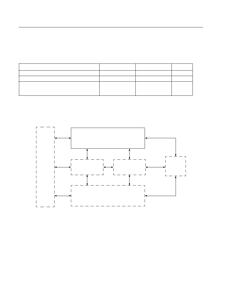
Application Information
Transceiver Interface
5-5967(F)
Figure 2. Typical Interface Application Diagram
Parameter
Min
Max
Unit
Junction Temperature Range
-
40
125
∞
C
V
DD
--
7.0
V
I
DD
(max):
Active
Powerdown
--
--
TBD
TBD
mA
mA
AUTONEGOTIATION
MANAGEMENT
100Base-TX OR 100Base-T4
PHYSICAL LAYER
MII
DNCX01
TP
MUX

Advance Data Sheet
DNCX01
September 1997
10Base-T Physical Interface ASIC Macrocell
Lucent Technologies Inc.
15
Application Information
(continued)
Using the Status Signals to Drive LEDs
The status signals can be taken out to registers or LED drivers. An example is illustrated in Figure 3.
5-5968(F)
Figure 3. LED Driver Example
STATUS
SIGNAL
BONxx
LED
(Dialight 555-2303 5 V LOW CURRENT
LED WITH INTERNAL RESISTOR)

DNCX01
Advance Data Sheet
10Base-T Physical Interface ASIC Macrocell
September 1997
Lucent Technologies Inc. reserves the right to make changes to the product(s) or information contained herein without notice. No liability is assumed as a result of their use or application. No
rights under any patent accompany the sale of any such product(s) or information.
Copyright © 1997 Lucent Technologies Inc.
All Rights Reserved
Printed in U.S.A.
September 1997
DS97-492ASIC (Replaces DS96-093ASIC)
Printed On
Recycled Paper
For additional information, contact your Microelectronics Group Account Manager or the following:
INTERNET:
http://www.lucent.com/micro
E-MAIL:
docmaster@micro.lucent.com
U.S.A.:
Microelectronics Group, Lucent Technologies Inc., 555 Union Boulevard, Room 30L-15P-BA, Allentown, PA 18103
1-800-372-2447, FAX 610-712-4106 (In CANADA: 1-800-553-2448, FAX 610-712-4106)
ASIA PACIFIC: Microelectronics Group, Lucent Technologies Singapore Pte. Ltd., 77 Science Park Drive, #03-18 Cintech III, Singapore 118256
Tel. (65) 778 8833, FAX (65) 777 7495
JAPAN:
Microelectronics Group, Lucent Technologies Japan Ltd., 7-18, Higashi-Gotanda 2-chome, Shinagawa-ku, Tokyo 141, Japan
Tel. (81) 3 5421 1600, FAX (81) 3 5421 1700
EUROPE:
Data Requests: MICROELECTRONICS GROUP DATALINE: Tel. (44) 1189 324 299, FAX (44) 1189 328 148
Technical Inquiries: GERMANY: (49) 89 95086 0 (Munich), UNITED KINGDOM: (44) 1344 865 900 (Bracknell),
FRANCE: (33) 1 41 45 77 00 (Paris), SWEDEN: (46) 8 600 7070 (Stockholm), FINLAND: (358) 9 4354 2800 (Helsinki),
ITALY: (39) 2 6601 1800 (Milan), SPAIN: (34) 1 807 1441 (Madrid)