 | –≠–Ľ–Ķ–ļ—ā—Ä–ĺ–Ĺ–Ĺ—č–Ļ –ļ–ĺ–ľ–Ņ–ĺ–Ĺ–Ķ–Ĺ—ā: DSP16411 | –°–ļ–į—á–į—ā—Ć:  PDF PDF  ZIP ZIP |

Data Sheet
May 2003
DSP16411 Digital Signal Processor
1 Features
!
Twin DSP16000 dual-MAC cores perform up to
1140 million MACs per second at 285 MHz
!
Low power:
-- 1.2 V internal supply for power efficiency
-- 3.3 V I/O pin supply for compatibility
!
322K x 16 on-chip RAM
!
Centralized direct memory access unit (DMAU):
-- Transparent peripheral-to-memory and mem-
ory-to-memory transfers
-- Better utilization of DSP MIPS
-- Simplifies management of system data flow
!
16-bit parallel interface unit (PIU) with direct mem-
ory access (DMA) provides host access to all DSP
memory
!
Two enhanced serial I/O units (SIU0 and SIU1)
with DMA:
-- Compatible with TDM highways such as T1/E1
and ST-bus
-- Hardware support for
Ķ
-law and A-law com-
panding
!
Core messaging units (MGU0 and MGU1) for inter-
processor communication
!
On-chip, programmable, PLL clock synthesizer
eliminates need for high-speed clock input
!
Two 7-bit control I/O interfaces (BIOs) for
increased flexibility and lower system costs
!
32-bit system and external memory interface
(SEMI) supports 16-bit or 32-bit synchronous or
asynchronous memories
!
Two IEEE
ģ
1149.1 test ports (JTAG boundary
scan)
!
Full-speed, in-circuit emulation hardware for each
core with eight address and two data watchpoint
units for efficient application development
!
Supported by DSP16411 software and hardware
development tools
!
208-ball PBGA package (17 mm x 17 mm; 1.0 mm
ball pitch) for small footprint
2 Description
The DSP16411 is a digital signal processor (DSP)
optimized for communications infrastructure applica-
tions. Large, on-chip memory enables it to be pro-
grammed to perform numerous fixed-point signal
processing functions, including equalization, chan-
nel coding, or speech coding. The DSP16411 fea-
tures twin DSP16000 dual-MAC DSP cores and
enhanced DMA capabilities. Together, these features
deliver the performance required for second- and
third-generation infrastructure equipment.
The DSP16411 extends the performance of the
DSP16410CG with a higher maximum clock rate and
additional on-chip RAM, while maintaining low power
consumption, efficient software code density, and
small physical size. The DSP16411 is pinout and
code compatible with the DSP16410CG to protect
investments in hardware and software development.

Data Sheet
DSP16411 Digital Signal Processor
May 2003
Table of Contents
Contents
Page
2
Agere Systems--Proprietary
Agere Systems Inc.
Use pursuant to Company instructions
"
1 Features ......................................................................................................................................................... 1
"
2 Description...................................................................................................................................................... 1
"
3 Notation Conventions ................................................................................................................................... 14
"
4 Hardware Architecture .................................................................................................................................. 14
"
4.1 DSP16411 Architectural Overview........................................................................................................ 14
"
4.1.1 DSP16000 Cores ........................................................................................................................ 17
"
4.1.2 Clock Synthesizer (PLL) ............................................................................................................. 17
"
4.1.3 Triport RAMs (TPRAM
0--1
)..................................................................................................... 17
"
4.1.4 Shared Local Memory (SLM) ......................................................................................................17
"
4.1.5 Internal Boot ROMs (IROM
0--1
) ............................................................................................. 17
"
4.1.6 Messaging Units (MGU
0--1
) ................................................................................................... 17
"
4.1.7 System and External Memory Interface (SEMI).......................................................................... 18
"
4.1.8 Bit Input/Output Units (BIO
0--1
) .............................................................................................. 18
"
4.1.9 Timer Units (TIMER0_
0--1
and TIMER1_
0--1
) ................................................................... 18
"
4.1.10 Direct Memory Access Unit (DMAU)........................................................................................... 18
"
4.1.11 Interrupt Multiplexers (IMUX
0--1
)............................................................................................ 18
"
4.1.12 Parallel Interface Unit (PIU) ........................................................................................................ 18
"
4.1.13 Serial Interface Units (SIU
0--1
) ...............................................................................................18
"
4.1.14 Test Access Ports (JTAG
0--1
)................................................................................................. 18
"
4.1.15 Hardware Development Systems (HDS
0--1
) .......................................................................... 18
"
4.2 DSP16000 Core Architectural Overview...............................................................................................19
"
4.2.1 System Control and Cache (SYS) .............................................................................................. 19
"
4.2.2 Data Arithmetic Unit (DAU) ......................................................................................................... 19
"
4.2.3 Y-Memory Space Address Arithmetic Unit (YAAU) .....................................................................20
"
4.2.4 X-Memory Space Address Arithmetic Unit (XAAU).....................................................................20
"
4.2.5 Core Block Diagram .................................................................................................................... 21
"
4.3 Device Reset ........................................................................................................................................ 23
"
4.3.1 Reset After Powerup or Power Interruption ................................................................................ 23
"
4.3.2 RSTN Pin Reset.......................................................................................................................... 23
"
4.3.3 JTAG Controller Reset ................................................................................................................ 24
"
4.4 Interrupts and Traps.............................................................................................................................. 25
"
4.4.1 Hardware Interrupt Logic ............................................................................................................25
"
4.4.2 Hardware Interrupt Multiplexing .................................................................................................. 28
"
4.4.3 Clearing Core Interrupt Requests ...............................................................................................30
"
4.4.4 Host Interrupt Output .................................................................................................................. 30
"
4.4.5 Globally Enabling and Disabling Hardware Interrupts................................................................. 30
"
4.4.6 Individually Enabling, Disabling, and Prioritizing Hardware Interrupts ........................................ 31
"
4.4.7 Hardware Interrupt Status ........................................................................................................... 32
"
4.4.8 Interrupt and Trap Vector Table................................................................................................... 32
"
4.4.9 Software Interrupts...................................................................................................................... 34
"
4.4.10 INT[3:0] and TRAP Pins.............................................................................................................. 34
"
4.4.11 Nesting Interrupts........................................................................................................................ 35
"
4.4.12 Interrupts and Cache Usage ....................................................................................................... 37
"
4.4.13 Interrupt Polling ........................................................................................................................... 37
"
4.5 Interprocessor Communication ............................................................................................................. 38
"
4.5.1 Core-to-Core Interrupts and Traps .............................................................................................. 39
"
4.5.2 Message Buffer Data Exchange ................................................................................................. 39
"
4.5.2.1
Message Buffer Write Protocol ................................................................................... 40
"
4.5.2.2
Message Buffer Read Protocol ................................................................................... 40
"
4.5.3 DMAU Data Transfer...................................................................................................................41
"
4.6 Memory Maps ....................................................................................................................................... 42

Table of Contents
(continued)
Contents
Page
Data Sheet
May 2003
DSP16411 Digital Signal Processor
Agere Systems Inc.
Agere Systems--Proprietary
3
Use pursuant to Company instructions
"
4.6.1 Private Internal Memory ..............................................................................................................43
"
4.6.2 Shared Internal I/O......................................................................................................................43
"
4.6.3 Shared External I/O and Memory................................................................................................43
"
4.6.4 X-Memory Map ...........................................................................................................................44
"
4.6.5 Y-Memory Maps ..........................................................................................................................45
"
4.6.6 Z-Memory Maps ..........................................................................................................................46
"
4.6.7 Internal I/O Detailed Memory Map ..............................................................................................47
"
4.7 Triport Random-Access Memory (TPRAM) ..........................................................................................48
"
4.8 Shared Local Memory (SLM) ................................................................................................................49
"
4.9 Bit Input/Output Units (BIO
0--1
) .......................................................................................................50
"
4.10 Timer Units (TIMER0_
0--1
and TIMER1_
0--1
) ............................................................................53
"
4.11 Hardware Development System (HDS
0--1
) .....................................................................................56
"
4.12 JTAG Test Port (JTAG
0--1
)...............................................................................................................57
"
4.12.1 Port Identification ........................................................................................................................57
"
4.12.2 Emulation Interface Signals to the DSP16411 ............................................................................58
"
4.12.2.1 TCS 14-Pin Header.....................................................................................................58
"
4.12.2.2 JCS 20-Pin Header .....................................................................................................59
"
4.12.2.3 HDS 9-Pin, D-Type Connector....................................................................................60
"
4.12.3 Multiprocessor JTAG Connections..............................................................................................61
"
4.12.4 Boundary Scan ...........................................................................................................................62
"
4.13 Direct Memory Access Unit (DMAU).....................................................................................................64
"
4.13.1 Overview .....................................................................................................................................64
"
4.13.2 Registers .....................................................................................................................................67
"
4.13.3 Data Structures ...........................................................................................................................83
"
4.13.3.1 One-Dimensional Data Structure (SWT Channels).....................................................83
"
4.13.3.2 Two-Dimensional Data Structure (SWT Channels) .....................................................84
"
4.13.3.3 Memory-to-Memory Block Transfers (MMT Channels) ...............................................86
"
4.13.4 The PIU Addressing Bypass Channel.........................................................................................86
"
4.13.5 Single-Word Transfer Channels (SWT).......................................................................................87
"
4.13.6 Memory-to-Memory Transfer Channels (MMT)...........................................................................90
"
4.13.7 Interrupts and Priority Resolution................................................................................................92
"
4.13.8 Error Reporting and Recovery ....................................................................................................94
"
4.13.9 Programming Examples..............................................................................................................95
"
4.13.9.1 SWT Example 1: A Two-Dimensional Array ...............................................................95
"
4.13.9.2 SWT Example 2: A One-Dimensional Array ...............................................................97
"
4.13.9.3 MMT Example .............................................................................................................99
"
4.14 System and External Memory Interface (SEMI)..................................................................................100
"
4.14.1 External Interface ......................................................................................................................101
"
4.14.1.1 Configuration.............................................................................................................102
"
4.14.1.2 Asynchronous Memory Bus Arbitration.....................................................................103
"
4.14.1.3 Enables and Strobes.................................................................................................104
"
4.14.1.4 External Clock...........................................................................................................105
"
4.14.1.5 Address and Data .....................................................................................................106
"
4.14.2 16-Bit External Bus Accesses ...................................................................................................109
"
4.14.3 32-Bit External Bus Accesses ...................................................................................................109
"
4.14.4 Registers ................................................................................................................................... 110
"
4.14.4.1 ECON0 Register ....................................................................................................... 111
"
4.14.4.2 ECON1 Register ....................................................................................................... 112
"
4.14.4.3 Segment Registers ................................................................................................... 114
"
4.14.5 Asynchronous Memory ............................................................................................................. 116
"
4.14.5.1 Functional Timing...................................................................................................... 116

Table of Contents
(continued)
Contents
Page
4
Agere Systems--Proprietary
Agere Systems Inc.
Use pursuant to Company instructions
Data Sheet
DSP16411 Digital Signal Processor
May 2003
"
4.14.5.2 Extending Access Time Via the ERDY Pin ............................................................... 120
"
4.14.5.3 Interfacing Examples ................................................................................................ 122
"
4.14.6 Synchronous Memory ............................................................................................................... 124
"
4.14.6.1 Functional Timing...................................................................................................... 124
"
4.14.6.2 Interfacing Examples ................................................................................................ 126
"
4.14.7 Performance ............................................................................................................................. 128
"
4.14.7.1 System Bus............................................................................................................... 128
"
4.14.7.2 External Memory, Asynchronous Interface ............................................................... 129
"
4.14.7.3 External Memory, Synchronous Interface ................................................................. 131
"
4.14.7.4 Summary of Access Times .......................................................................................133
"
4.14.8 Priority ....................................................................................................................................... 134
"
4.15 Parallel Interface Unit (PIU) ................................................................................................................ 135
"
4.15.1 Registers ...................................................................................................................................135
"
4.15.2 Hardware Interface ................................................................................................................... 139
"
4.15.2.1 Enables and Strobes................................................................................................. 140
"
4.15.2.2 Address and Data Pins .............................................................................................141
"
4.15.2.3 Flags, Interrupt, and Ready Pins .............................................................................. 142
"
4.15.3 Host Data Read and Write Cycles ............................................................................................ 143
"
4.15.4 Host Register Read and Write Cycles.......................................................................................145
"
4.15.5 Host Commands .......................................................................................................................147
"
4.15.5.1 Status/Control/Address Register Read Commands.................................................. 148
"
4.15.5.2 Status/Control/Address Register Write Commands .................................................. 148
"
4.15.5.3 Memory Read Commands ........................................................................................ 149
"
4.15.5.4 Flow Control for Memory Read Commands.............................................................. 150
"
4.15.5.5 Memory Write Commands ........................................................................................ 151
"
4.15.5.6 Flow Control for Control/Status/Address Register and Memory Write Commands...151
"
4.15.6 Host Command Examples ........................................................................................................ 152
"
4.15.6.1 Download of Program or Data .................................................................................. 152
"
4.15.6.2 Upload of Data ..........................................................................................................152
"
4.15.7 PIU Interrupts ............................................................................................................................ 153
"
4.16 Serial Interface Unit (SIU) ................................................................................................................... 154
"
4.16.1 Hardware Interface ................................................................................................................... 156
"
4.16.2 Pin Conditioning Logic, Bit Clock Selection Logic, and Frame Sync Selection Logic ............... 157
"
4.16.3 Basic Input Processing ............................................................................................................. 159
"
4.16.4 Basic Output Processing........................................................................................................... 160
"
4.16.5 Clock and Frame Sync Generation ........................................................................................... 161
"
4.16.6 ST-Bus Timing Examples..........................................................................................................166
"
4.16.7 SIU Loopback ........................................................................................................................... 168
"
4.16.8 Basic Frame Structure .............................................................................................................. 168
"
4.16.9 Assigning SIU Logical Channels to DMAU Channels ............................................................... 169
"
4.16.10 Frame Error Detection and Reporting .......................................................................................170
"
4.16.11 Frame Mode.............................................................................................................................. 170
"
4.16.12 Channel Mode--32 Channels or Less in Two Subframes or Less ........................................... 171
"
4.16.13 Channel Mode--Up to 128 Channels in a Maximum of Eight Subframes ................................ 177
"
4.16.14 SIU Examples ........................................................................................................................... 180
"
4.16.14.1 Single-Channel I/O....................................................................................................180
"
4.16.14.2 ST-Bus Interface ....................................................................................................... 181
"
4.16.15 Registers ...................................................................................................................................184
"
4.17 Internal Clock Selection ...................................................................................................................... 200
"
4.18 Clock Synthesis .................................................................................................................................. 201
"
4.18.1 PLL Operating Frequency ......................................................................................................... 201

Table of Contents
(continued)
Contents
Page
Data Sheet
May 2003
DSP16411 Digital Signal Processor
Agere Systems Inc.
Agere Systems--Proprietary
5
Use pursuant to Company instructions
"
4.18.2 PLL LOCK Flag Generation ......................................................................................................201
"
4.18.3 PLL Registers ...........................................................................................................................202
"
4.18.4 PLL Programming Example ......................................................................................................203
"
4.18.5 Powering Down the PLL ...........................................................................................................203
"
4.18.6 Phase-Lock Loop (PLL) Frequency Accuracy and Jitter...........................................................203
"
4.19 External Clock Selection .....................................................................................................................204
"
4.20 Power Management............................................................................................................................205
"
5 Processor Boot-Up and Memory Download ...............................................................................................208
"
5.1 IROM Boot Routine and Host Download Via PIU ...............................................................................208
"
5.2 EROM Boot Routine and DMAU Download........................................................................................209
"
6 Software Architecture .................................................................................................................................210
"
6.1 Instruction Set Quick Reference .........................................................................................................210
"
6.1.1 Conditions Based on the State of Flags ....................................................................................226
"
6.2 Registers.............................................................................................................................................227
"
6.2.1 Directly Program-Accessible (Register-Mapped) Registers......................................................227
"
6.2.2 Memory-Mapped Registers.......................................................................................................231
"
6.2.3 Register Encodings ...................................................................................................................235
"
6.2.4 Reset States..............................................................................................................................249
"
6.2.5 RB Field Encoding ....................................................................................................................252
"
7 208-Ball PBGA Package Ball Assignments ................................................................................................253
"
8 Signal Descriptions .....................................................................................................................................256
"
8.1 System Interface .................................................................................................................................257
"
8.2 BIO Interface.......................................................................................................................................257
"
8.3 System and External Memory Interface..............................................................................................257
"
8.4 SIU0 Interface .....................................................................................................................................260
"
8.5 SIU1 Interface .....................................................................................................................................261
"
8.6 PIU Interface .......................................................................................................................................262
"
8.7 JTAG0 Test Interface ..........................................................................................................................263
"
8.8 JTAG1 Test Interface ..........................................................................................................................263
"
8.9 Power and Ground..............................................................................................................................264
"
9 Device Characteristics ................................................................................................................................265
"
9.1 Absolute Maximum Ratings ................................................................................................................265
"
9.2 Handling Precautions..........................................................................................................................265
"
9.3 Recommended Operating Conditions.................................................................................................265
"
9.3.1 Package Thermal Considerations .............................................................................................266
"
10 Electrical Characteristics and Requirements ..............................................................................................267
"
10.1 Maintenance of Valid Logic Levels for Bidirectional Signals and Unused Inputs ................................268
"
10.1.1 Maintenance of Valid Logic Levels on the SEMI Interface ........................................................268
"
10.1.2 Maintenance of Valid Logic Levels on the PIU Interface...........................................................270
"
10.2 Analog Power Supply Decoupling.......................................................................................................271
"
10.3 Power Dissipation ...............................................................................................................................272
"
10.3.1 Internal Power Dissipation ........................................................................................................272
"
10.3.2 I/O Power Dissipation................................................................................................................273
"
10.4 Power Supply Sequencing..................................................................................................................275
"
11 Timing Charateristics and Requirements....................................................................................................276
"
11.1 Phase-Lock Loop ................................................................................................................................277
"
11.2 Wake-Up Latency ...............................................................................................................................278
"
11.3 DSP Clock Generation........................................................................................................................279
"
11.4 Reset Circuit .......................................................................................................................................280
"
11.5 Reset Synchronization ........................................................................................................................281
"
11.6 JTAG ...................................................................................................................................................282

Table of Contents
(continued)
Contents
Page
6
Agere Systems--Proprietary
Agere Systems Inc.
Use pursuant to Company instructions
Data Sheet
DSP16411 Digital Signal Processor
May 2003
"
11.7 Interrupt and Trap ............................................................................................................................... 283
"
11.8 Bit I/O .................................................................................................................................................. 284
"
11.9 System and External Memory Interface.............................................................................................. 285
"
11.9.1 Asynchronous Interface ............................................................................................................ 286
"
11.9.2 Synchronous Interface .............................................................................................................. 289
"
11.9.3 ERDY Interface ......................................................................................................................... 291
"
11.10 PIU ......................................................................................................................................................292
"
11.11 SIU ......................................................................................................................................................296
"
12 Appendix--Naming Inconsistencies ........................................................................................................... 306
"
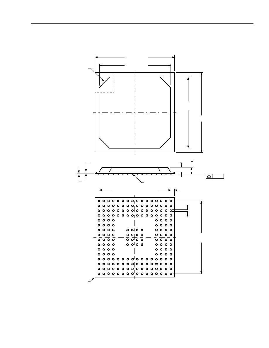
13 Outline Diagram--208-Ball PBGA .............................................................................................................. 307
"
14 Index ........................................................................................................................................................... 308

List of Figures
Figure
Page
Data Sheet
May 2003
DSP16411 Digital Signal Processor
Agere Systems Inc.
Agere Systems--Proprietary
7
Use pursuant to Company instructions
"
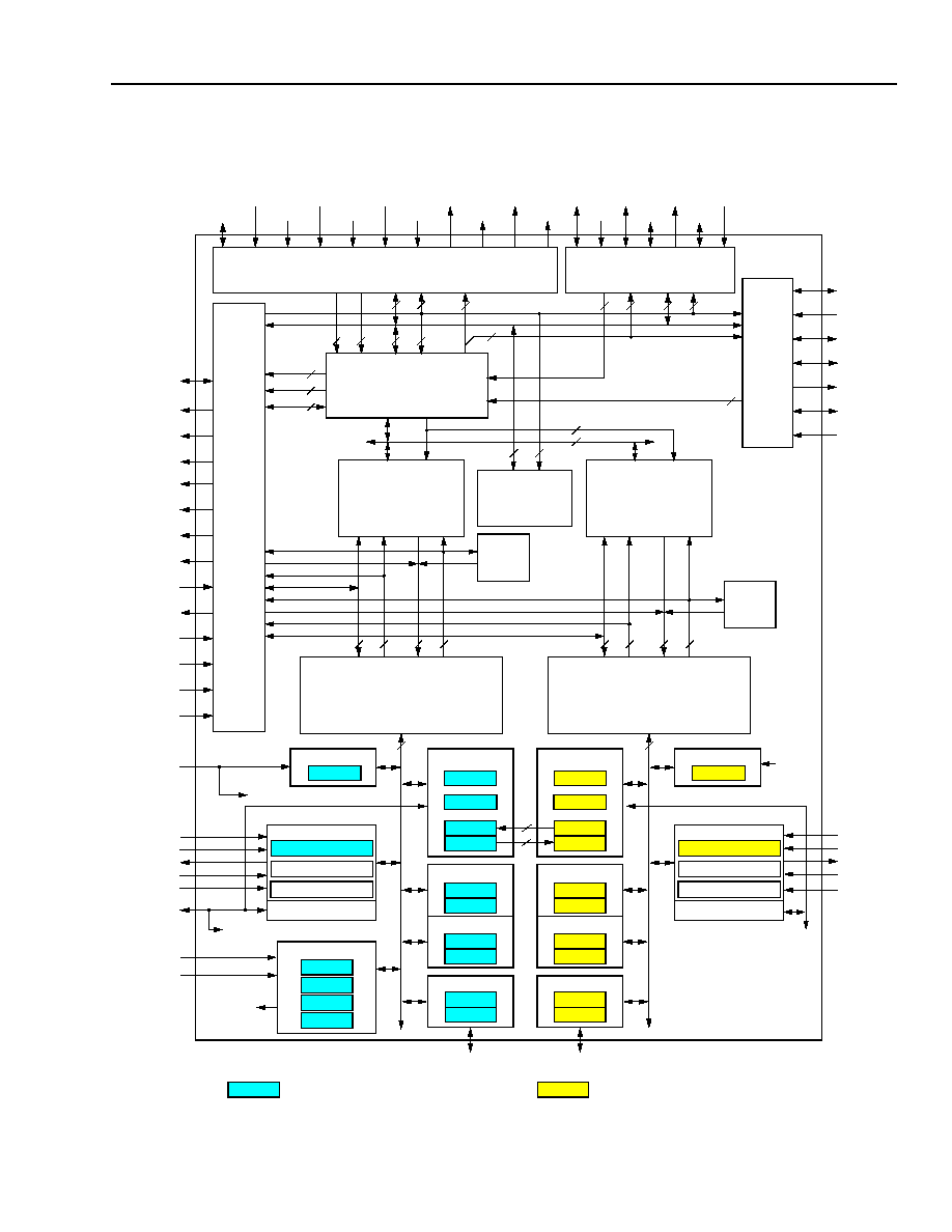
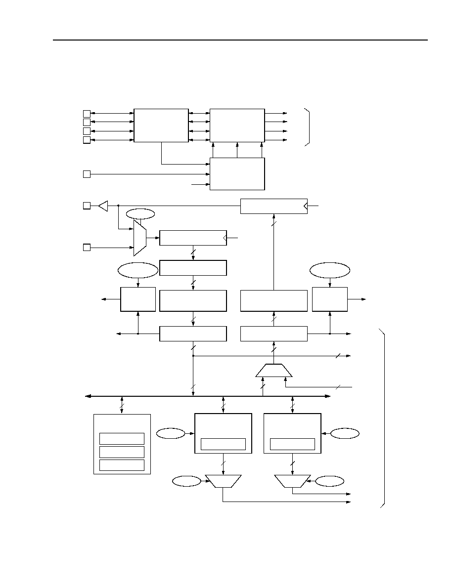
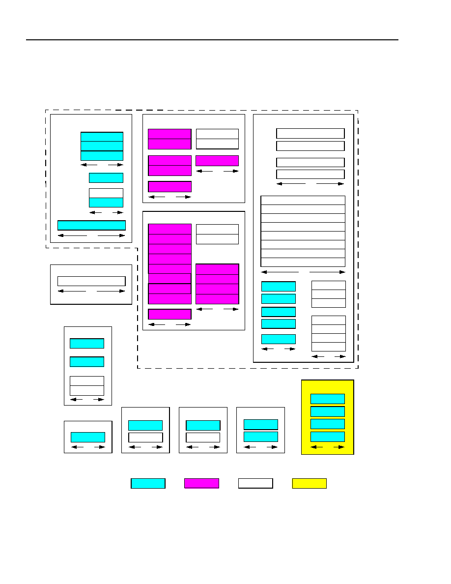
Figure 1. DSP16411 Block Diagram ..................................................................................................................15
"
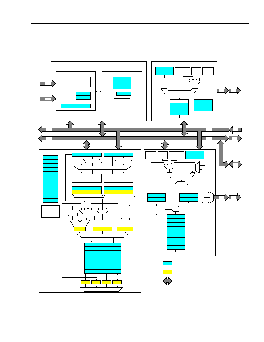
Figure 2. DSP16000 Core Block Diagram .........................................................................................................21
"
Figure 3. CORE0 and CORE1 Interrupt Logic Block Diagram...........................................................................26
"
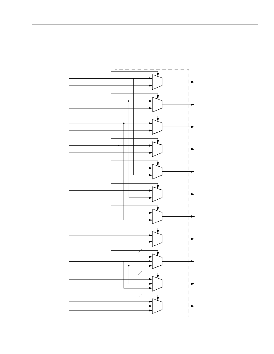
Figure 4. IMUX Block Diagram ..........................................................................................................................29
"
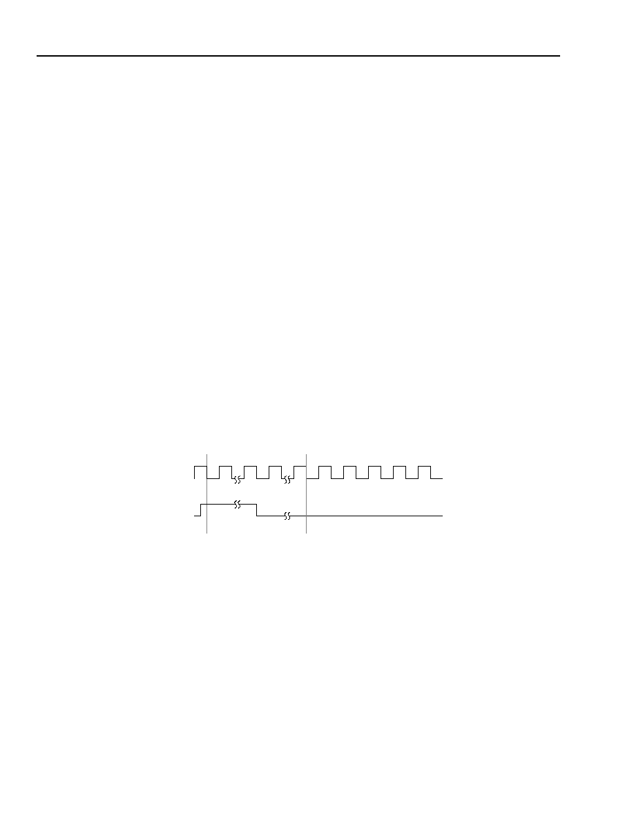
Figure 5. Functional Timing for INT[3:0] and TRAP ...........................................................................................34
"
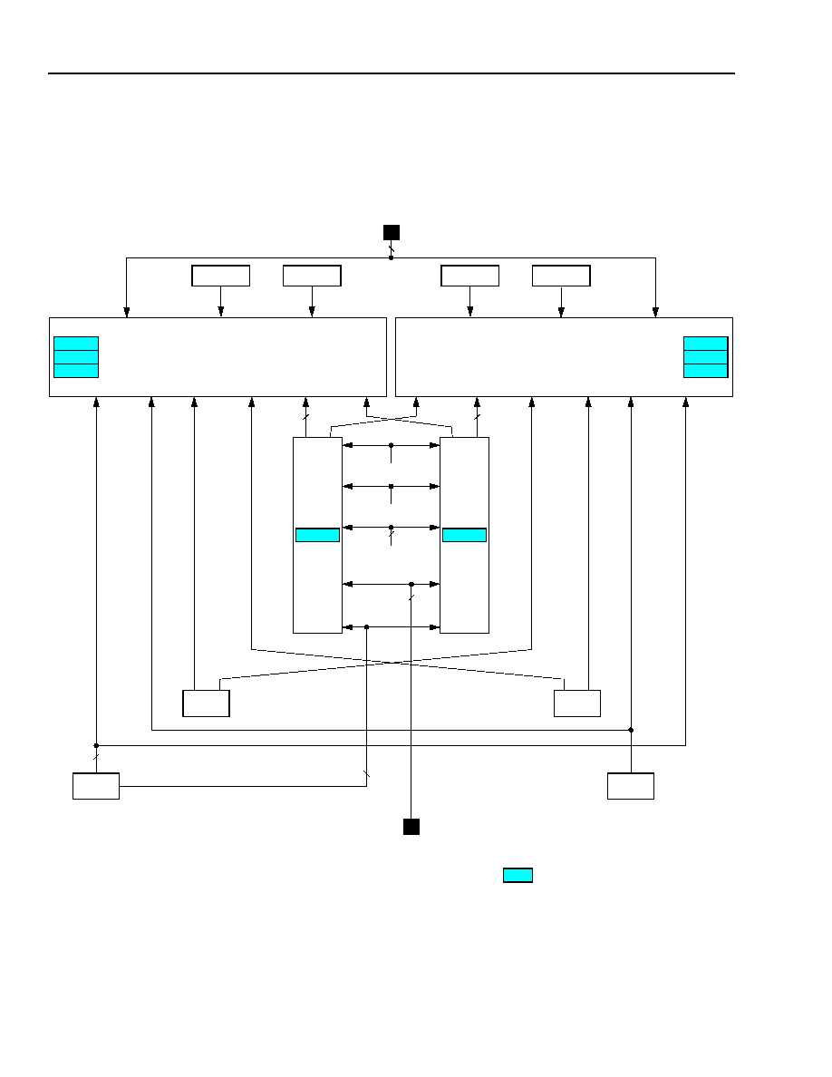
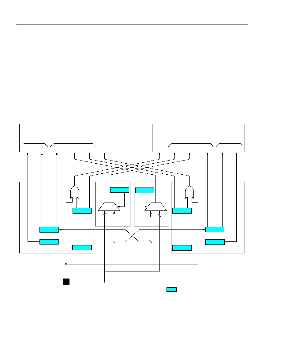
Figure 6. Interprocessor Communication Logic in MGU0 and MGU1................................................................38
"
Figure 7. X-Memory Map ...................................................................................................................................44
"
Figure 8. Y-Memory Maps .................................................................................................................................45
"
Figure 9. Z-Memory Maps..................................................................................................................................46
"
Figure 10. Internal I/O Memory Map ....................................................................................................................47
"
Figure 11. Interleaved Internal TPRAM ...............................................................................................................48
"
Figure 12. Example Memory Arrangement ..........................................................................................................48
"
Figure 13. Timer Block Diagram ..........................................................................................................................54
"
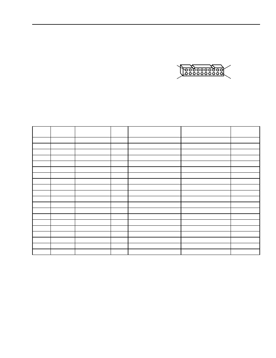
Figure 14. TCS 14-Pin Connector........................................................................................................................58
"
Figure 15. JCS 20-Pin Connector ........................................................................................................................59
"
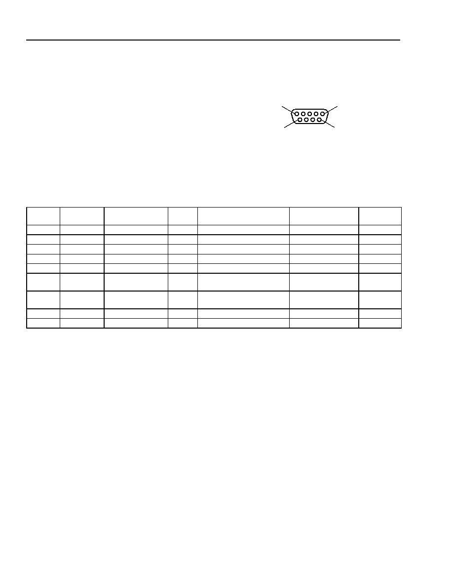
Figure 16. HDS 9-Pin Connector .........................................................................................................................60
"
Figure 17. Typical Multiprocessor JTAG Connection with Single Scan Chain.....................................................61
"
Figure 18. DMAU Interconnections and Channels...............................................................................................65
"
Figure 19. DMAU Block Diagram .........................................................................................................................66
"
Figure 20. One-Dimensional Data Structure for Buffering n Channels ................................................................83
"
Figure 21. Two-Dimensional Data Structure for Double-Buffering n Channels....................................................84
"
Figure 22. Memory-to-Memory Block Transfer ....................................................................................................86
"
Figure 23. Example of a Two-Dimensional Double-Buffered Data Structure.......................................................95
"
Figure 24. Example of One-Dimensional Data Structure .....................................................................................97
"
Figure 25. Memory-to-Memory Block Transfer ....................................................................................................99
"
Figure 26. SEMI Interface Block Diagram..........................................................................................................100
"
Figure 27. Asynchronous Memory Cycles .........................................................................................................117
"
Figure 28. Asynchronous Memory Cycles (RSETUP = 1, WSETUP = 1)..........................................................118
"
Figure 29. Asynchronous Memory Cycles (RHOLD = 1, WHOLD = 1)..............................................................119
"
Figure 30. Use of ERDY Pin to Extend Asynchronous Accesses ......................................................................120
"
Figure 31. Example of Using the ERDY Pin ......................................................................................................121
"
Figure 32. 32-Bit External Interface with 16-Bit Asynchronous SRAMs ............................................................123
"
Figure 33. 16-Bit External Interface with 16-Bit Asynchronous SRAMs ............................................................123
"
Figure 34. Synchronous Memory Cycles ...........................................................................................................125
"
Figure 35. 16-Bit External Interface with 16-Bit Pipelined, Synchronous ZBT SRAMs......................................126
"
Figure 36. 32-Bit External Interface with 32-Bit Pipelined, Synchronous ZBT SRAMs......................................127
"
Figure 37. 32-Bit PA Register Host and Core Access........................................................................................138
"
Figure 38. PIU Functional Timing for a Data Read and Write Operation ...........................................................144
"
Figure 39. PIU Functional Timing for a Register Read and Write Operation .....................................................146
"
Figure 40. SIU Block Diagram ...........................................................................................................................155
"
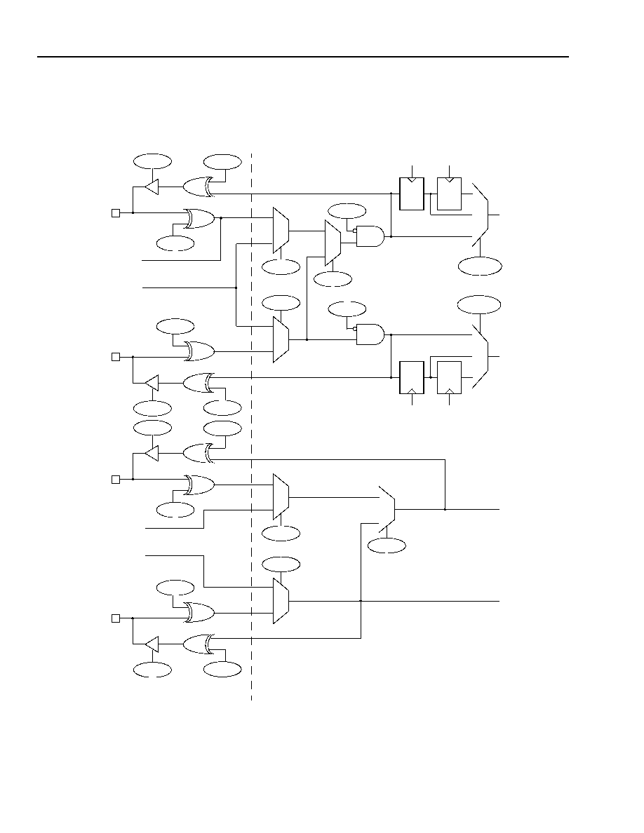
Figure 41. Pin Conditioning Logic, Bit Clock Selection Logic, and Frame Sync Selection Logic.......................158
"
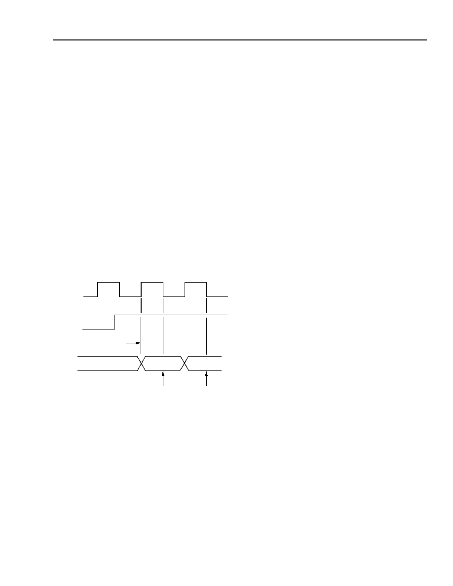
Figure 42. Default Serial Input Functional Timing ..............................................................................................159
"
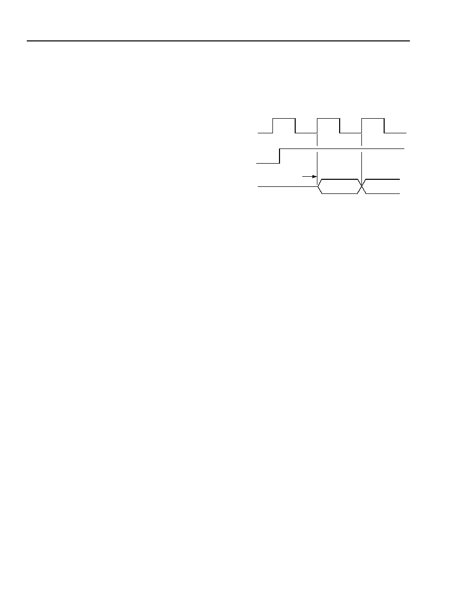
Figure 43. Default Serial Output Functional Timing ...........................................................................................160
"
Figure 44. Frame Sync to Data Delay Timing ....................................................................................................163
"
Figure 45. Clock and Frame Sync Generation with External Clock and Synchronization
(AGEXT = AGSYNC = IFSA = IFSK = 1 and Timing Requires No Resynchronization) ...................166
"
Figure 46. Clock and Frame Sync Generation with External Clock and Synchronization
(AGEXT = AGSYNC = IFSA = IFSK = 1 and Timing Requires Resynchronization) .........................167
"
Figure 47. Basic Frame Structure ......................................................................................................................168
"
Figure 48. Basic Frame Structure with Idle Time ...............................................................................................169
"
Figure 49. Channel Mode on a 128-Channel Frame .........................................................................................171

List of Figures
(continued)
Data Sheet
DSP16411 Digital Signal Processor
May 2003
Figure
Page
8
Agere Systems--Proprietary
Agere Systems Inc.
Use pursuant to Company instructions
"
Figure 50. Subframe and Channel Selection in Channel Mode ......................................................................... 176
"
Figure 51. Generating Interrupts on Subframe Boundaries ............................................................................... 178
"
Figure 52. ST-Bus Single-Rate Clock ................................................................................................................ 183
"
Figure 53. ST-Bus Double-Rate Clock............................................................................................................... 183
"
Figure 54. Internal Clock Selection Logic ..........................................................................................................200
"
Figure 55. Clock Synthesizer (PLL) Block Diagram ........................................................................................... 201
"
Figure 56. Power Management and Clock Distribution...................................................................................... 206
"
Figure 57. Interpretation of the Instruction Set Summary Table ........................................................................ 211
"
Figure 58. DSP16411 Program-Accessible Registers for Each Core ................................................................ 228
"
Figure 59. Example Memory-Mapped Registers ............................................................................................... 231
"
Figure 60. 208-Ball PBGA Package Ball Grid Array Assignments (See-Through Top View) ............................ 253
"
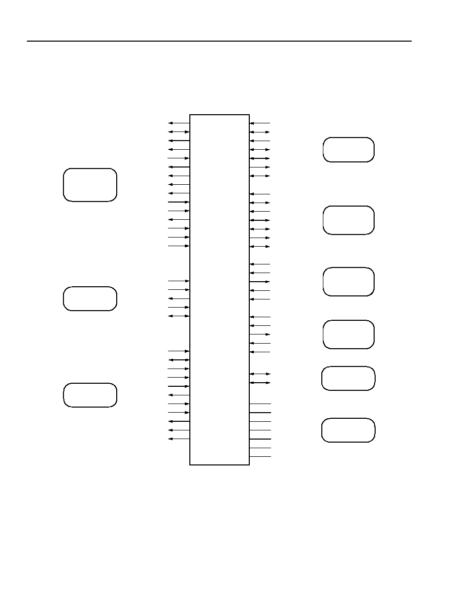
Figure 61. DSP16411 Pinout by Interface ......................................................................................................... 256
"
Figure 62. Analog Supply Decoupling................................................................................................................ 271
"
Figure 63. Reference Voltage Level for Timing Characteristics and Requirements for Inputs and Outputs...... 276
"
Figure 64. I/O Clock Timing Diagram.................................................................................................................279
"
Figure 65. Powerup and Device Reset Timing Diagram ................................................................................... 280
"
Figure 66. Reset Synchronization Timing ..........................................................................................................281
"
Figure 67. JTAG I/O Timing Diagram ............................................................................................................... 282
"
Figure 68. Interrupt and Trap Timing Diagram................................................................................................... 283
"
Figure 69. Write Outputs Followed by Read Inputs (cbit = IMMEDIATE; a1 = sbit) Timing Characteristics .... 284
"
Figure 70. Enable and Write Strobe Transition Timing ...................................................................................... 285
"
Figure 71. Timing Diagram for EREQN and EACKN ......................................................................................... 286
"
Figure 72. Asynchronous Read Timing Diagram (RHOLD = 0 and RSETUP = 0) ............................................ 287
"
Figure 73. Asynchronous Write Timing Diagram (WHOLD = 0, WSETUP = 0) ................................................. 288
"
Figure 74. Synchronous Read Timing Diagram (Read-Read-Write Sequence) ................................................289
"
Figure 75. Synchronous Write Timing Diagram ................................................................................................. 290
"
Figure 76. ERDY Pin Timing Diagram ............................................................................................................... 291
"
Figure 77. Host Data Write to PDI Timing Diagram ........................................................................................... 292
"
Figure 78. Host Data Read from PDO Timing Diagram ..................................................................................... 293
"
Figure 79. Host Register Write (PAH, PAL, PCON, or HSCRATCH) Timing Diagram ...................................... 294
"
Figure 80. Host Register Read (PAH, PAL, PCON, or DSCRATCH) Timing Diagram ...................................... 295
"
Figure 81. SIU Passive Frame and Channel Mode Input Timing Diagram ........................................................ 296
"
Figure 82. SIU Passive Frame Mode Output Timing Diagram........................................................................... 297
"
Figure 83. SIU Passive Channel Mode Output Timing Diagram........................................................................ 298
"
Figure 84. SCK External Clock Source Input Timing Diagram ..........................................................................299
"
Figure 85. SIU Active Frame and Channel Mode Input Timing Diagram ........................................................... 300
"
Figure 86. SIU Active Frame Mode Output Timing Diagram ............................................................................. 302
"
Figure 87. SIU Active Channel Mode Output Timing Diagram ..........................................................................303
"
Figure 88. ST-Bus 2x Input Timing Diagram...................................................................................................... 304
"
Figure 89. ST-Bus 2x Output Timing Diagram ................................................................................................... 305

List of Tables
Table
Page
Agere Systems Inc.
Agere Systems--Proprietary
9
Use pursuant to Company instructions
Data Sheet
May 2003
DSP16411 Digital Signal Processor
"
Table 1.
DSP16411 Block Diagram Legend ..................................................................................................16
"
Table 2.
DSP16000 Core Block Diagram Legend..........................................................................................22
"
Table 3.
State of Device Output and Bidirectional Pins During and After Reset ............................................24
"
Table 4.
Hardware Interrupts .........................................................................................................................27
"
Table 5.
imux (Interrupt Multiplex Control) Register ......................................................................................28
"
Table 6.
Global Disabling and Enabling of Hardware Interrupts ....................................................................30
"
Table 7.
inc0 and inc1 (Interrupt Control) Registers 0 and 1 ........................................................................31
"
Table 8.
ins (Interrupt Status) Register..........................................................................................................32
"
Table 9.
Interrupt and Trap Vector Table .......................................................................................................33
"
Table 10.
psw1 (Processor Status Word 1) Register ......................................................................................35
"
Table 11.
signal Register ................................................................................................................................39
"
Table 12.
Full-Duplex Data Transfer Code Through Core-to-Core Message Buffer ........................................40
"
Table 13.
DMAU MMT Channel Interrupts .......................................................................................................41
"
Table 14.
DMA Intracore and Intercore Transfers Example.............................................................................41
"
Table 15.
DSP16411 Memory Components ....................................................................................................42
"
Table 16.
sbit (BIO Status/Control) Register ...................................................................................................50
"
Table 17.
cbit (BIO Control) Register ..............................................................................................................51
"
Table 18.
BIO Operations ................................................................................................................................52
"
Table 19.
BIO Flags .........................................................................................................................................52
"
Table 20.
timer
0,1
c (TIMER
0,1
Control) Register.....................................................................................55
"
Table 21.
timer
0,1
(TIMER
0,1
Running Count) Register ..........................................................................56
"
Table 22.
ID (JTAG Identification) Register .....................................................................................................57
"
Table 23.
TCS 14-Pin Socket Pinout ...............................................................................................................58
"
Table 24.
JCS 20-Pin Socket Pinout ................................................................................................................59
"
Table 25.
HDS 9-Pin, Subminiature, D-Type Plug Pinout ................................................................................60
"
Table 26.
JTAG0 Boundary-Scan Register ......................................................................................................62
"
Table 27.
JTAG1 Boundary-Scan Register ......................................................................................................63
"
Table 28.
DMAU Channel Assignment ............................................................................................................64
"
Table 29.
DMAU Memory-Mapped Registers ..................................................................................................67
"
Table 30.
DSTAT (DMAU Status) Register ......................................................................................................69
"
Table 31.
DMCON0 (DMAU Master Control 0) Register..................................................................................71
"
Table 32.
DMCON1 (DMAU Master Control 1) Register..................................................................................72
"
Table 33.
Collective Designations Used in Table 34........................................................................................73
"
Table 34.
CTL
0--3
(SWT
0--3
Control) Registers .....................................................................................74
"
Table 35.
Collective Designations Used in Table 36........................................................................................76
"
Table 36.
CTL
4--5
(MMT
4--5
Control) Registers .....................................................................................76
"
Table 37.
SADD
0--5
and DADD
0--5
(Channels 0--5 Source and Destination Address) Registers ........77
"
Table 38.
SCNT
0--3
(SWT
0--3
Source Counter) Registers .....................................................................78
"
Table 39.
SCNT
4--5
(MMT
4--5
Source Counter) Registers.....................................................................78
"
Table 40.
DCNT
0--3
(SWT
0--3
Destination Counter) Registers ..............................................................79
"
Table 41.
DCNT
4--5
(MMT
4--5
Destination Counter) Registers ..............................................................79
"
Table 42.
LIM
0--3
(SWT
0--3
Limit) Registers ..........................................................................................80
"
Table 43.
LIM
4--5
(MMT
4--5
Limit) Registers..........................................................................................80
"
Table 44.
SBAS
0--3
(SWT
0--3
Source Base Address) Registers ...........................................................81
"
Table 45.
DBAS
0--3
(SWT
0--3
Destination Base Address) Registers ....................................................81
"
Table 46.
STR
0--3
(SWT
0--3
Stride) Registers .......................................................................................82
"
Table 47.
RI
0--3
(SWT
0--3
Reindex) Registers .......................................................................................82
"
Table 48.
SWT-Specific Memory-Mapped Registers .......................................................................................88
"
Table 49.
MMT-Specific Memory-Mapped Registers .......................................................................................91
"
Table 50.
DMAU Interrupts ..............................................................................................................................92
"
Table 51.
Overview of SEMI Pins ..................................................................................................................101

List of Tables
(continued)
Table
Page
Data Sheet
DSP16411 Digital Signal Processor
May 2003
10
Agere Systems--Proprietary
Agere Systems Inc.
Use pursuant to Company instructions
"
Table 52.
Configuration Pins for the SEMI External Interface........................................................................ 102
"
Table 53.
Asynchronous Memory Bus Arbitration Pins .................................................................................. 103
"
Table 54.
Enable and Strobe Pins for the SEMI External Interface ............................................................... 104
"
Table 55.
ECKO Output Clock Pin Configuration........................................................................................... 105
"
Table 56.
Address and Data Bus Pins for the SEMI External Interface ......................................................... 107
"
Table 57.
16-Bit External Bus Configuration .................................................................................................. 109
"
Table 58.
32-Bit External Bus Configuration .................................................................................................. 109
"
Table 59.
SEMI Memory-Mapped Registers .................................................................................................. 110
"
Table 60.
ECON0 (External Control 0) Register ............................................................................................ 111
"
Table 61.
ECON1 (External Control 1) Register ............................................................................................ 112
"
Table 62.
ECKO Output Clock Pin Configuration........................................................................................... 113
"
Table 63.
EXSEG0 (CORE0 External X Segment Address Extension) Register........................................... 114
"
Table 64.
EXSEG1 (CORE1 External X Segment Address Extension) Register........................................... 114
"
Table 65.
EYSEG0 (CORE0 External Y Segment Address Extension) Register........................................... 115
"
Table 66.
EYSEG1 (CORE1 External Y Segment Address Extension) Register........................................... 115
"
Table 67.
System Bus Minimum Access Times .............................................................................................128
"
Table 68.
Access Time Per SEMI Transaction, Asynchronous Interface, 32-Bit Data Bus ........................... 133
"
Table 69.
Access Time Per SEMI Transaction, Asynchronous Interface, 16-Bit Data Bus ........................... 133
"
Table 70.
Access Time Per SEMI Transaction, Synchronous Interface, 32-Bit Data Bus .............................133
"
Table 71.
Access Time Per SEMI Transaction, Synchronous Interface, 16-Bit Data Bus .............................133
"
Table 72.
Example Average Access Time Per SEMI Transaction, 32-Bit Data Bus ...................................... 134
"
Table 73.
Example Average Access Time Per SEMI Transaction, 16-Bit Data Bus ...................................... 134
"
Table 74.
PIU Registers ................................................................................................................................. 135
"
Table 75.
PCON (PIU Control) Register ........................................................................................................ 136
"
Table 76.
PDI (PIU Data In) Register ............................................................................................................. 137
"
Table 77.
PDO (PIU Data Out) Register ........................................................................................................ 137
"
Table 78.
HSCRATCH (Host Scratch) Register .............................................................................................137
"
Table 79.
DSCRATCH (DSP Scratch) Register .............................................................................................137
"
Table 80.
PA (Parallel Address) Register....................................................................................................... 138
"
Table 81.
PIU External Interface .................................................................................................................... 139
"
Table 82.
Enable and Strobe Pins .................................................................................................................140
"
Table 83.
Address and Data Pins .................................................................................................................. 141
"
Table 84.
Flags, Interrupt, and Ready Pins....................................................................................................142
"
Table 85.
Summary of Host Commands ........................................................................................................ 147
"
Table 86.
Status/Control/Address Register Read Commands ....................................................................... 148
"
Table 87.
Status/Control/Address Register Write Commands ....................................................................... 148
"
Table 88.
Memory Read Commands ............................................................................................................. 149
"
Table 89.
Memory Write Commands ............................................................................................................. 151
"
Table 90.
SIU External Interface .................................................................................................................... 156
"
Table 91.
Control Register Fields for Pin Conditioning, Bit Clock Selection, and Frame Sync Selection ...... 157
"
Table 92.
A Summary of Bit Clock and Frame Sync Control Register Fields ................................................164
"
Table 93.
Examples of Bit Clock and Frame Sync Control Register Fields ................................................... 165
"
Table 94.
Subframe Definition........................................................................................................................ 172
"
Table 95.
Location of Control Fields Used in Channel Mode ......................................................................... 174
"
Table 96.
Description of Control Fields Used in Channel Mode .................................................................... 174
"
Table 97.
Subframe Selection ........................................................................................................................ 175
"
Table 98.
Channel Activation Within a Selected Subframe............................................................................ 175
"
Table 99.
Channel Masking Within a Selected Subframe .............................................................................. 175
"
Table 100. Control Register and Field Configuration for ST-Bus Interface ...................................................... 181
"
Table 101. Control Register and Fields That Are Configured as Required for ST-Bus Interface..................... 182
"
Table 102. SIU Registers ................................................................................................................................. 184

List of Tables
(continued)
Table
Page
Agere Systems Inc.
Agere Systems--Proprietary
11
Use pursuant to Company instructions
Data Sheet
May 2003
DSP16411 Digital Signal Processor
"
Table 103. SCON0 (SIU Input/Output General Control) Register ....................................................................185
"
Table 104. SCON1 (SIU Input Frame Control) Register ..................................................................................186
"
Table 105. SCON2 (SIU Output Frame Control) Register ...............................................................................187
"
Table 106. SCON3 (SIU Input/Output Subframe Control) Register .................................................................188
"
Table 107. SCON4 (SIU Input Even Subframe Valid Vector Control) Register ...............................................189
"
Table 108. SCON5 (SIU Input Odd Subframe Valid Vector Control) Register.................................................189
"
Table 109. SCON6 (SIU Output Even Subframe Valid Vector Control) Register.............................................190
"
Table 110. SCON7 (SIU Output Odd Subframe Valid Vector Control) Register ..............................................190
"
Table 111. SCON8 (SIU Output Even Subframe Mask Vector Control) Register ............................................190
"
Table 112. SCON9 (SIU Output Odd Subframe Mask Vector Control) Register .............................................190
"
Table 113. SCON10 (SIU Input/Output General Control) Register ..................................................................191
"
Table 114. SCON11 (SIU Input/Output Active Clock Control) Register ...........................................................194
"
Table 115. SCON12 (SIU Input/Output Active Frame Sync Control) Register.................................................195
"
Table 116. SIDR (SIU Input Data) Register .....................................................................................................196
"
Table 117. SODR (SIU Output Data) Register.................................................................................................196
"
Table 118. STAT (SIU Input/Output General Status) Register .........................................................................197
"
Table 119. FSTAT (SIU Input/Output Frame Status) Register .........................................................................197
"
Table 120. OCIX
0--1
and ICIX
0--1
(SIU Output and Input Channel Index) Registers .............................198
"
Table 121. OCIX
0--1
(SIU Output Channel Index) Registers ......................................................................198
"
Table 122. ICIX
0--1
(SIU Input Channel Index) Registers ...........................................................................199
"
Table 123. Source Clock Selection ..................................................................................................................200
"
Table 124. pllcon (Phase-Lock Loop Control) Register ..................................................................................202
"
Table 125. pllfrq (Phase-Lock Loop Frequency Control) Register ..................................................................202
"
Table 126. pllfrq1 (Phase-Lock Loop Frequency Control 1) Register .............................................................202
"
Table 127. plldly (Phase-Lock Loop Delay Control) Register .........................................................................202
"
Table 128. ECKO Output Clock Pin Configuration...........................................................................................204
"
Table 129. Wake-Up Latency and Power Consumption for Low-Power Standby Mode ..................................207
"
Table 130. Core Boot-Up After Reset ..............................................................................................................208
"
Table 131. Contents of IROM0 and IROM1 Boot ROMs .................................................................................208
"
Table 132. DSP16411 Instruction Groups .......................................................................................................210
"
Table 133. Instruction Set Summary ................................................................................................................212
"
Table 134. Notation Conventions for Instruction Set Descriptions ...................................................................218
"
Table 135. Overall Replacement Table............................................................................................................219
"
Table 136. F1 Instruction Syntax .....................................................................................................................222
"
Table 137. F1E Function Statement Syntax ....................................................................................................224
"
Table 138. DSP16411 Conditional Mnemonics ...............................................................................................226
"
Table 139. Program-Accessible (Register-Mapped) Registers by Type, Listed Alphabetically .......................229
"
Table 140. DMAU Memory-Mapped Registers ................................................................................................232
"
Table 141. SEMI Memory-Mapped Registers ..................................................................................................233
"
Table 142. PIU Registers .................................................................................................................................234
"
Table 143. SIU Memory-Mapped Registers .....................................................................................................234
"
Table 144. alf (AWAIT Low-Power and Flag) Register ....................................................................................235
"
Table 145. auc0 (Arithmetic Unit Control 0) Register ......................................................................................236
"
Table 146. auc1 (Arithmetic Unit Control 1) Register ......................................................................................237
"
Table 147. cbit (BIO Control) Register ............................................................................................................238
"
Table 148. cloop (Cache Loop) Register ........................................................................................................239
"
Table 149. csave (Cache Save) Register ........................................................................................................239
"
Table 150. cstate (Cache State) Register .......................................................................................................239
"
Table 151. imux (Interrupt Multiplex Control) Register ....................................................................................240
"
Table 152. ID (JTAG
0--1
Identification) Registers .......................................................................................241
"
Table 153. inc0 and inc1 (Interrupt Control) Registers 0 and 1 ......................................................................241

List of Tables
(continued)
Table
Page
Data Sheet
DSP16411 Digital Signal Processor
May 2003
12
Agere Systems--Proprietary
Agere Systems Inc.
Use pursuant to Company instructions
"
Table 154. ins (Interrupt Status) Register........................................................................................................ 242
"
Table 155. mgi (Core-to-Core Message Input) Register ................................................................................. 242
"
Table 156. mgo (Core-to-Core Message Output) Register ............................................................................. 242
"
Table 157. pid (Processor Identification) Register........................................................................................... 242
"
Table 158. pllcon (Phase-Lock Loop Control) Register .................................................................................. 243
"
Table 159. pllfrq (Phase-Lock Loop Frequency Control) Register .................................................................. 243
"
Table 160. pllfrq1 (Phase-Lock Loop Frequency Control 1) Register .............................................................243
"
Table 161. plldly (Phase-Lock Loop Delay Control) Register ......................................................................... 243
"
Table 162. psw0 (Processor Status Word 0) Register .................................................................................... 244
"
Table 163. psw1 (Processor Status Word 1) Register .................................................................................... 245
"
Table 164. sbit (BIO Status/Control) Register ................................................................................................. 246
"
Table 165. signal (Core-to-Core Signal) Register ........................................................................................... 246
"
Table 166. timer0c and timer1c (TIMER
0,1
Control) Registers .................................................................. 247
"
Table 167. timer0 and timer1 (TIMER
0,1
Running Count) Registers .......................................................... 248
"
Table 168. vsw (Viterbi Support Word) Register .............................................................................................248
"
Table 169. Core Register States After Reset--40-Bit Registers...................................................................... 249
"
Table 170. Core Register States After Reset--32-Bit Registers...................................................................... 249
"
Table 171. Core Register States After Reset--20-Bit Registers...................................................................... 250
"
Table 172. Core Register States After Reset--16-Bit Registers...................................................................... 250
"
Table 173. Off-Core (Peripheral) Register Reset Values ................................................................................. 250
"
Table 174. Memory-Mapped Register Reset Values--32-Bit Registers .......................................................... 251
"
Table 175. Memory-Mapped Register Reset Values--20-Bit Registers .......................................................... 251
"
Table 176. Memory-Mapped Register Reset Values--16-Bit Registers .......................................................... 251
"
Table 177. RB Field .........................................................................................................................................252
"
Table 178. 208-Ball PBGA Ball Assignments Sorted Alphabetically by Symbol .............................................. 254
"
Table 179. Absolute Maximum Ratings ........................................................................................................... 265
"
Table 180. Minimum ESD Voltage Thresholds ................................................................................................ 265
"
Table 181. Recommended Operating Conditions ............................................................................................ 265
"
Table 182. Package Thermal Considerations .................................................................................................. 266
"
Table 183. Electrical Characteristics and Requirements ................................................................................. 267
"
Table 184. Effect of EYMODE Pin and BHEDIS Field ..................................................................................... 269
"
Table 185. Typical Internal Power Dissipation at 1.2 V and 285 MHz .............................................................272
"
Table 186. Typical I/O Power Dissipation at 3.3 V and 285 MHz .................................................................... 274
"
Table 187. Reference Voltage Level for Timing Characteristics and Requirements for Inputs and Outputs ...276
"
Table 188. PLL Requirements ......................................................................................................................... 277
"
Table 189. Wake-Up Latency........................................................................................................................... 278
"
Table 190. Timing Requirements for Input Clock .............................................................................................279
"
Table 191. Timing Characteristics for Output Clock......................................................................................... 279
"
Table 192. Timing Requirements for Powerup and Device Reset ...................................................................280
"
Table 193. Timing Characteristics for Device Reset ........................................................................................ 280
"
Table 194. Timing Requirements for Reset Synchronization Timing ............................................................... 281
"
Table 195. Timing Requirements for JTAG I/O ................................................................................................ 282
"
Table 196. Timing Characteristics for JTAG I/O .............................................................................................. 282
"
Table 197. Timing Requirements for Interrupt and Trap .................................................................................. 283
"
Table 198. Timing Requirements for BIO Input Read ...................................................................................... 284
"
Table 199. Timing Characteristics for BIO Output ........................................................................................... 284
"
Table 200. Timing Characteristics for ERWN and Memory Enables................................................................ 285
"
Table 201. Timing Requirements for EREQN .................................................................................................. 286
"
Table 202. Timing Characteristics for EACKN and SEMI Bus Disable ............................................................ 286
"
Table 203. Timing Requirements for Asynchronous Memory Read Operations .............................................. 287
"
Table 204. Timing Characteristics for Asynchronous Memory Read Operations ............................................ 287

List of Tables
(continued)
Table
Page
Agere Systems Inc.
Agere Systems--Proprietary
13
Use pursuant to Company instructions
Data Sheet
May 2003
DSP16411 Digital Signal Processor
"
Table 205. Timing Characteristics for Asynchronous Memory Write Operations.............................................288
"
Table 206. Timing Requirements for Synchronous Read Operations..............................................................289
"
Table 207. Timing Characteristics for Synchronous Read Operations ............................................................289
"
Table 208. Timing Characteristics for Synchronous Write Operations.............................................................290
"
Table 209. Timing Requirements for ERDY Pin...............................................................................................291
"
Table 210. Timing Requirements for PIU Data Write Operations .................................................................... 292
"
Table 211. Timing Characteristics for PIU Data Write Operations ...................................................................292
"
Table 212. Timing Requirements for PIU Data Read Operations ....................................................................293
"
Table 213. Timing Characteristics for PIU Data Read Operations...................................................................293
"
Table 214. Timing Requirements for PIU Register Write Operations...............................................................294
"
Table 215. Timing Characteristics for PIU Register Write Operations .............................................................295
"
Table 216. Timing Requirements for PIU Register Read Operations ..............................................................295
"
Table 217. Timing Characteristics for PIU Register Read Operations .............................................................295
"
Table 218. Timing Requirements for SIU Passive Frame Mode Input .............................................................296
"
Table 219. Timing Requirements for SIU Passive Channel Mode Input ..........................................................296
"
Table 220. Timing Requirements for SIU Passive Frame Mode Output ..........................................................297
"
Table 221. Timing Characteristics for SIU Passive Frame Mode Output.........................................................297
"
Table 222. Timing Requirements for SIU Passive Channel Mode Output .......................................................298
"
Table 223. Timing Characteristics for SIU Passive Channel Mode Output......................................................298
"
Table 224. Timing Requirements for SCK External Clock Source ...................................................................299
"
Table 225. Timing Requirements for SIU Active Frame Mode Input................................................................300
"
Table 226. Timing Characteristics for SIU Active Frame Mode Input ..............................................................300
"
Table 227. Timing Requirements for SIU Active Channel Mode Input.............................................................301
"
Table 228. Timing Characteristics for SIU Active Channel Mode Input ...........................................................301
"
Table 229. Timing Requirements for SIU Active Frame Mode Output .............................................................302
"
Table 230. Timing Characteristics for SIU Active Frame Mode Output............................................................302
"
Table 231. Timing Requirements for SIU Active Channel Mode Output ..........................................................303
"
Table 232. Timing Characteristics for SIU Active Channel Mode Output.........................................................303
"
Table 233. ST-Bus 2x Input Timing Requirements ..........................................................................................304
"
Table 234. ST-Bus 2x Output Timing Requirements .......................................................................................305
"
Table 235. ST-Bus 2x Output Timing Characteristics ......................................................................................305
"
Table 236. Pin Name Inconsistencies ..............................................................................................................306
"
Table 237. Register Name Inconsistencies......................................................................................................306

Data Sheet
DSP16411 Digital Signal Processor
May 2003
14
Agere Systems--Proprietary
Agere Systems Inc.
Use pursuant to Company instructions
3 Notation Conventions
The following notation conventions apply to this data
sheet.
Table 134 on page 218
specifies the notation
conventions for the DSP16000 instruction set.
lower-case
Registers that are directly writable or
readable by DSP16411 core instruc-
tions are lower-case.
UPPER-CASE Device flags, I/O pins, control register
fields, and registers that are not directly
writable or readable by DSP16411 core
instructions are upper-case.
boldface
Register names and DSP16411 core
instructions are printed in boldface
when used in text descriptions.
italics
Documentation variables that are
replaced are printed in italics.
courier
DSP16411 program examples or
C-language representations are printed
in courier font.
[ ]
Square brackets enclose a range of
numbers that represents multiple bits in
a single register or bus. The range of
numbers is delimited by a colon. For
example, imux[11:10] are bits 11 and
10 of the program-accessible imux reg-
ister.
Angle brackets enclose a list of items
delimited by commas or a range of
items delimited by a dash (--), one of
which is selected if used in an
instruction. For example, SADD
0--3
represents the four memory-mapped
registers SADD0, SADD1, SADD2,
and SADD3, and the general instruc-
tion aTE
h,l
= RB can be replaced
with a0h = timer0.
blue
In this document, blue text or the blue
graphic object
"
indicates a hypertext
link. Click on the text or
"
to display
the referenced item.
4 Hardware Architecture
4.1 DSP16411 Architectural Overview
The DSP16411 device is a 16-bit fixed-point program-
mable digital signal processor (DSP). The DSP16411
consists of two DSP16000 cores together with on-chip
memory and peripherals. Advanced architectural fea-
tures with an expanded instruction set deliver a dra-
matic increase in performance compared to traditional
DSP architectures for signal coding algorithms. This
increase in performance, together with an efficient
design implementation, results in an extremely cost-
efficient and power-efficient solution for wireless and
multimedia applications.
Figure 1 on page 15
shows a block diagram of the
DSP16411.

Data Sheet
May 2003
DSP16411 Digital Signal Processor
Agere Systems Inc.
Agere Systems--Proprietary
15
Use pursuant to Company instructions
4 Hardware Architecture
(continued)
4.1 DSP16411 Architectural Overview
(continued)
DSP16411B Block Diagram
Figure 1. DSP16411 Block Diagram
YDB YAB
XDB XAB
YDB YAB
XDB XAB
IDB
XAB0
XDB0
YAB0
YDB0
YAB1
YDB1
32
20
32
32
20
32
20
CORE0
SAB
SDB
ZEAB
ZEDB
ZIDB
ZIAB
SDB SAB
ZEDB
ZEAB
SDB SAB
32
20
TPRAM0
IROM0
PAB DPI
27
16
PIU
SIU0
DMAU
DSI0
DSI1
IMUX0
imux
32
MGU0
signal
jiob
BOUNDARY SCAN
JTAG0
TIMER0_0
TIMER1_0
TIMER0_1
TIMER1_1
32
BIO0
pid
16
16
HDS0
cbit
PD[15:0]
PODS
PCSN
PIDS
PADD[3:0]
PRWN
PRDYMD
POBE
PIBF
PRDY
PINT
SDB
SAB
SIU1
SICK0
SID0
SIFS0
SOCK0
SOD0
SOFS0
SCK0
SICK1
SID1
SIFS1
SOCK1
SOD1
SOFS1
SCK1
ED[31:0]
EA[18:0]
ERAMN
EROMN
EION
ERWN[1:0]
ECKO
EREQN
EACKN
ERDY
EXM
ERTYPE
ESIZE
INT[3:0]
TCK0
TMS0
TDO0
TDI0
TRST0N
CKI
RSTN
TRAP
IO0BIT[6:0]
IO1BIT[6:0]
TCK1
TMS1
TDO1
TDI1
TRST1N
INT[3:0]
SEMI
CLK
DDO
DDO
DDO
DSI
DSI
DDO
XAB
XDB
YAB
YDB
IDB
CORE1
(160K x 16)
MGU1
IMUX1
imux
CLOCK/CONTROL
pllcon
20
XAB1
XDB1
ZSEG
ZSEG
4
YDB YAB
XDB XAB
ZIDB
ZIAB
TPRAM1
(160K x 16)
IROM1
SLM
(2K x 16)
32
20
SDB SAB
32
20
PAB DPI
32
ESEG[3:0]
16
16
20
32
16
16
BIO1
SDB SAB
32
20
TO IMUX1
TO HDS1/MGU1
TRAP
ZIAB
ZIDB
sbit
cbit
timer1
timer1c
timer1
timer1c
timer0
timer0c
timer0
timer0c
mgi
mgo
mgo
mgi
signal
pid
20
32
ID
pllfrq
plldly
jiob
BOUNDARY SCAN
JTAG1
HDS1
ID
KEY:
OFF-CORE REGISTER-MAPPED REGISTERS
ACCESSIBLE BY CORE0
sbit
OFF-CORE REGISTER-MAPPED REGISTERS
ACCESSIBLE BY CORE1
pllfrq1

Data Sheet
DSP16411 Digital Signal Processor
May 2003
16
Agere Systems--Proprietary
Agere Systems Inc.
Use pursuant to Company instructions
4 Hardware Architecture
(continued)
4.1 DSP16411 Architectural Overview
(continued)
Table 1. DSP16411 Block Diagram Legend
Symbol
Description
BIO
0--1
Bit I/O Units. One for each core.
cbit
16-Bit BIO Control Register.
CLK
Internal Clock Signal.
CORE0
DSP16000 Core--System Master.
CORE1
DSP16000 Core--System Slave.
DDO
DMA Data Out. (For transferring data from DMAU to PIU, SIU0, and SIU1.)
DMAU
Direct Memory Access Unit.
DPI
DMA Parallel In. (For transferring 16-bit data from PIU to DMAU.)
DSI0
DMA Serial Data In Zero. (For transferring data from SIU0 to DMAU.)
DSI1
DMA Serial Data In One. (For transferring data from SIU1 to DMAU.)
HDS
0--1
Hardware Development Systems. One for each core.
ID
JTAG Port Identification Register Accessible Via the JTAG Port. One for each of the two JTAG
0--1
ports.
IDB
Internal Data Bus. One for each core.
imux
16-Bit IMUX Control Register.
IMUX
0--1
Interrupt Multiplexers. One for each core; selects ten interrupts from DMAU, SIU0, SIU1, PIU, INT[3:0],
TIMER
0--1
, and MGU.
IROM
0--1
Internal Read-Only Memories (one for each core) for Boot and HDS Code.
jiob
32-Bit JTAG Test Register.
JTAG
0--1
JTAG Test Ports. One for each core.
mgi
16-Bit Core-to-Core Message Input Register.
mgo
16-Bit Core-to-Core Message Output Register.
MGU
0--1
Core-to-Core Messaging Unit. One for each core.
PAB
27-Bit Parallel Address Bus. (For DMAU/PIU communications.)
pid
16-Bit Processor ID Register (CORE0: 0x0000; CORE1: 0x0001).
PIU
Parallel Interface Unit. (16-bit parallel host interface.)
pllcon
16-Bit Phase-Lock Loop Control Register.
pllfrq
16-Bit Phase-Lock Loop Frequency Control Register.
pllfrq1
16-Bit Phase-Lock Loop Frequency Control 1 Register.
plldly
16-Bit Phase-Lock Loop Delay Control Register.
SAB
20-Bit System Address Bus. Address for system bus (S-bus) accesses.
sbit
16-Bit BIO Status/Control Register.
SDB
32-Bit System Data Bus. Data for system bus (S-bus) accesses.
SEMI
System and External Memory Interface.
signal
16-Bit Signal Register for Core-to-Core Communication.
SIU0
Serial Input/Output Unit Zero.
SIU1
Serial Input/Output Unit One.
SLM
2 Kword Shared Local Memory.
timer0
16-Bit Timer Running Count Register for TIMER0.
TIMER0_0
Programmable Timer 0 for CORE0.
TIMER0_1
Programmable Timer 0 for CORE1.
timer0c
16-Bit Timer Control Register for TIMER0.
timer1
16-Bit Timer Running Count Register for TIMER1.
TIMER1_0
Programmable Timer 1 for CORE0.
TIMER1_1
Programmable Timer 1 for CORE1.

Table 1. DSP16411 Block Diagram Legend (continued)
Data Sheet
May 2003
DSP16411 Digital Signal Processor
Agere Systems Inc.
Agere Systems--Proprietary
17
Use pursuant to Company instructions
4 Hardware Architecture
(continued)
4.1 DSP16411 Architectural Overview
(continued)
4.1.1 DSP16000 Cores
The two DSP16000 cores (CORE0 and CORE1) are
the signal-processing engines of the DSP16411. The
DSP16000 is a modified Harvard architecture with sep-
arate sets of buses for the instruction/coefficient
(X-memory) and data (Y-memory) spaces. Each set of
buses has 20 bits of address and 32 bits of data. The
core contains data and address arithmetic units and
control for on-chip memory and peripherals.
4.1.2 Clock Synthesizer (PLL)
The DSP16411 powers up with an input clock (CKI) as
the source for the processor clock (CLK). An on-chip
clock synthesizer (PLL) that runs at a frequency multi-
ple of CKI can also be used to generate CLK. The
clock synthesizer is deselected and powered down on
reset. The selection of the clock source is under soft-
ware control of CORE0. See
Section 4.17, beginning
on page 200,
for details.
4.1.3 Triport RAMs (TPRAM
0--1
)
Each core has a private block of TPRAM consisting of
160 banks (banks 0--159) of zero wait-state memory.
Each bank consists of 1K 16-bit words and has three
separate address and data ports: one port to the core's
instruction/coefficient (X-memory) space, a second
port to the core's data (Y-memory) space, and a third
port to the DMA (Z-memory) space. TPRAM0 is
accessible by CORE0, TPRAM1 is accessible by
CORE1, and both TPRAM0 and TPRAM1 are accessi-
ble by the DMAU. TPRAM is organized into even and
odd interleaved banks for which each even/odd
address pair is a 32-bit wide module (see
Section 4.7
on page 48
for details). The TPRAMs support single-
word, aligned double-word, and misaligned double-
word accesses.
4.1.4 Shared Local Memory (SLM)
The SLM consists of two banks of memory. Each bank
consists of 1K 16-bit words. The SLM can be
accessed by both cores and by the DMAU and PIU
over the system bus (SAB, SDB). The SLM supports
single-word (16-bit) and aligned double-word (32-bit)
accesses. Misaligned double-word accesses are not
supported. An access to the SLM takes multiple clock
cycles to complete, and a core access to the SLM
causes the core to incur wait-states. See
Section 4.14.7.1 on page 128
for details on system bus
performance.
4.1.5 Internal Boot ROMs (IROM
0--1
)
Each core has its own boot ROM that contains a single
boot routine and software to support the Agere hard-
ware development system (HDS). The code in IROM0
and IROM1 is identical. See
Section 5 on page 208
for
details.
4.1.6 Messaging Units (MGU
0--1
)
The DSP16411 provides an MGU for each core: MGU0
for CORE0 and MGU1 for CORE1. The MGUs provide
interprocessor (core-to-core) communication and inter-
rupt generation. See
Section 4.5 on page 38
for
details.
timer1c
16-Bit Timer Control Register for TIMER1.
TPRAM
0--1
160 Kword Three-Port Random-Access Memories (one for each core). Private code (X), data (Y), and
DMA (Z).
XAB
0--1
20-Bit X-Memory Space Address Bus. One for each core.
XDB
0--1
32-Bit X-Memory Space Data Bus. One for each core.
YAB
0--1
20-Bit Y-Memory Space Address Bus. One for each core.
YDB
0--1
32-Bit Y-Memory Space Data Bus. One for each core.
ZEAB
20-Bit External Z-Memory Space Address Bus. Interfaces DMAU to SEMI.
ZEDB
32-Bit External Z-Memory Space Data Bus. Interfaces DMAU to SEMI.
ZIAB
20-Bit Internal Z-Memory Space Address Bus. Interfaces DMAU to TPRAM0 and TPRAM1.
ZIDB
32-Bit Internal Z-Memory Space Data Bus. Interfaces DMAU to TPRAM0 and TPRAM1.
ZSEG
External Segment Address Bits Associated with ZEAB. Interfaces DMAU to SEMI.
Symbol
Description

Data Sheet
DSP16411 Digital Signal Processor
May 2003
18
Agere Systems--Proprietary
Agere Systems Inc.
Use pursuant to Company instructions
4 Hardware Architecture
(continued)
4.1 DSP16411 Architectural
Overview
(continued)
4.1.7 System and External Memory Interface
(SEMI)
The SEMI interfaces both cores and the DMAU to
external memory and I/O devices. It interfaces directly
to pipelined synchronous ZBT TM
SRAMs and asyn-
chronous SRAMs. The SEMI also interfaces the cores
and the DMAU to the internal SLM and to memory-
mapped registers in the DMAU, PIU, SIU0, and SIU1
via the internal system bus or S-bus (SAB and
SDB). See
Section 4.14, beginning on page 100,
for
details.
4.1.8 Bit Input/Output Units (BIO
0--1
)
The DSP16411 provides a BIO unit for each core: BIO0
for CORE0 and BIO1 for CORE1. Each BIO unit pro-
vides convenient and efficient monitoring and control of
seven individually configurable pins. If configured as
outputs, the pins can be individually set, cleared, or
toggled. If configured as inputs, individual pins or com-
binations of pins can be tested for patterns. Flags
returned by the BIO can be tested by conditional
instructions. See
Section 4.9 on page 50
for details.
4.1.9 Timer Units (TIMER0_
0--1
and
TIMER1_
0--1
)
The DSP16411 provides two timer units for each core:
TIMER0_0 and TIMER1_0 for CORE0, and TIMER0_1
and TIMER1_1 for CORE1. Each timer can be used to
provide an interrupt, either single or repetitive, at the
expiration of a programmed interval. More than nine
orders of magnitude of interval selection are provided.
See
Section 4.10 on page 53
for more information.
4.1.10 Direct Memory Access Unit (DMAU)
The direct memory access unit (DMAU) manages data
transfers in the DSP16411 memory space. Data can
be moved between DSP16411 memory and peripher-
als and between different memory spaces in the
DSP16411. Once initiated, DMAU transfers occur with-
out core intervention. The DMAU supports concurrent
core execution and I/O processing. See
Section 4.13,
beginning on page 64,
for details.
4.1.11 Interrupt Multiplexers (IMUX
0--1
)
The DSP16411 provides an interrupt multiplexer unit
for each core: IMUX0 for CORE0 and IMUX1 for
CORE1. Each IMUX multiplexes the 26 hardware
interrupts into the 20 available hardware interrupt
requests for each core. See
Section 4.4.2 on page 28
for details.
4.1.12 Parallel Interface Unit (PIU)
The parallel interface unit (PIU) is a 16-bit parallel port
that provides a host processor direct access to the
entire DSP16411 memory system (including memory-
mapped peripheral registers). See
Section 4.15,
beginning on page 135,
for details.
4.1.13 Serial Interface Units (SIU
0--1
)
The DSP16411 provides two identical SIUs. Each SIU
is a full-duplex, double-buffered serial port with inde-
pendent input and output frame and bit clock control.
Clock and frame signals can be generated externally
(passive) or by on-chip clock and frame generation
hardware (active). The SIU features multiple-channel
TDM mode for ST-bus (1x and 2x compatible) and
T1/E1 compatibility. Each SIU is provided a DMAU
interface for data transfer to memory (TPRAM0,
TPRAM1, SLM, memory-mapped registers, or external
memory) without core intervention. See
Section 4.16,
beginning on page 154,
for details.
4.1.14 Test Access Ports (JTAG
0--1
)
The DSP16411 provides a JTAG unit for each core:
JTAG0 for CORE0 and JTAG1 for CORE1. See
Section 4.12 on page 57
for details.
4.1.15 Hardware Development Systems
(HDS
0--1
)
The DSP16411 provides an HDS unit for each core:
HDS0 for CORE0 and HDS1 for CORE1. Each HDS is
an on-chip hardware module available for debugging
assembly-language programs that execute on the
DSP16000 core in real-time. The main capability of the
HDS is in allowing controlled visibility into the core's
state during program execution. The HDS is enhanced
with powerful debugging capabilities such as complex
breakpointing conditions, multiple data/address watch-
point registers, and an intelligent trace mechanism for
recording discontinuities. See
Section 4.11 on page 56
for details.

Data Sheet
May 2003
DSP16411 Digital Signal Processor
Agere Systems Inc.
Agere Systems--Proprietary
19
Use pursuant to Company instructions
4 Hardware Architecture
(continued)
4.2 DSP16000 Core Architectural Overview
The DSP16411 contains two identical DSP16000
cores. As shown in
Figure 2 on page 21
, each core
consists of four major blocks: system control and cache
(SYS), data arithmetic unit (DAU), Y-memory space
address arithmetic unit (YAAU), and X-memory space
address arithmetic unit (XAAU). Bits within the auc0
and auc1 registers configure the DAU mode-controlled
operations. See the DSP16000 Digital Signal Proces-
sor Core Information Manual for a complete description
of the DSP16000 core.
4.2.1 System Control and Cache (SYS)
This section consists of the control block and the
cache.
The control block provides overall system coordination
that is mostly invisible to the user. The control block
includes an instruction decoder and sequencer, a
pseudorandom sequence generator (PSG), an inter-
rupt and trap handler, a wait-state generator, and low-
power standby mode control logic. An interrupt and trap
handler provides a user-locatable vector table and
three levels of user-assigned interrupt priority.
SYS contains the alf register, which is a 16-bit register
that contains AWAIT, a power-saving standby mode
bit, and peripheral flags. The inc0 and inc1 registers
are 20-bit interrupt control registers, and ins is a 20-bit
interrupt status register.
Programs use the instruction cache to store and exe-
cute repetitive operations such as those found in an
FIR or IIR filter section. The cache can contain up to
thirty-one 16-bit and 32-bit instructions. The code in the
cache can repeat up to 2
16
≠ 1 times without looping
overhead. Operations in the cache that require a coeffi-
cient access execute at twice the normal rate because
the XAAU and its associated bus are not needed for
fetching instructions. The cache greatly reduces the
need for writing in-line repetitive code and, therefore,
reduces instruction/coefficient memory size require-
ments. In addition, the use of cache reduces power
consumption because it eliminates memory accesses
for instruction fetches.
The cache provides a convenient, low-overhead loop-
ing structure that is interruptible, savable, and restor-
able. The cache is addressable in both the X and Y
memory spaces. An interrupt or trap handling routine
can save and restore cloop, cstate, csave, and the
contents of the cache. The cloop register controls the
cache loop count. The cstate register contains the cur-
rent state of the cache. The 32-bit csave register holds
the opcode of the instruction following the loop instruc-
tion in program memory.
4.2.2 Data Arithmetic Unit (DAU)
The DAU is a power-efficient, dual-MAC (multiply/accu-
mulate), parallel-pipelined structure that is tailored to
communications applications. It can perform two dou-
ble-word (32-bit) fetches, two multiplications, and two
accumulations in a single instruction cycle. The dual-
MAC parallel pipeline begins with two 32-bit registers,
x and y. The pipeline treats the 32-bit registers as four
16-bit signed registers if used as input to two signed
16-bit x 16-bit multipliers. Each multiplier produces a
full 32-bit result stored into registers p0 and p1. The
DAU can direct the output of each multiplier to a 40-bit
ALU or a 40-bit 3-input ADDER. The ALU and ADDER
results are each stored in one of eight 40-bit accumula-
tors, a0 through a7. Both the ALU and ADDER include
an ACS (add/compare/select) function for Viterbi
decoding. The DAU can direct the output of each accu-
mulator to the ALU/ACS, the ADDER/ACS, or a 40-bit
BMU (bit manipulation unit).
The ALU implements 2-input addition, subtraction, and
various logical operations. The ADDER implements
2-input or 3-input addition and subtraction. To support
Viterbi decoding, the ALU and ADDER have a split
mode in which two simultaneous 16-bit additions or
subtractions are performed. This mode, available in
specialized dual-MAC instructions, is used to compute
the distance between a received symbol and its esti-
mate.
The ACS provides the add/compare/select function
required for Viterbi decoding. This unit provides flags to
the traceback encoder for implementing mode-con-
trolled side-effects for ACS operations. The source
operands for the ACS are any two accumulators, and
results are written back to one of the source accumula-
tors.
The BMU implements barrel-shift, bit-field insertion, bit-
field extraction, exponent extraction, normalization, and
accumulator shuffling operations. ar0 through ar3 are
auxiliary registers whose main function is to control
BMU operations.
The user can enable overflow saturation to affect the
multiplier output and the results of the three arithmetic
units. Overflow saturation can also affect an accumula-
tor value as it is transferred to memory or other
register. These features accommodate various speech
coding standards such as GSM-FR, GSM-HR, and
GSM-EFR. Shifting in the arithmetic pipeline occurs at
several stages to accommodate various standards for
mixed-precision and double-precision multiplications.

Data Sheet
DSP16411 Digital Signal Processor
May 2003
20
Agere Systems--Proprietary
Agere Systems Inc.
Use pursuant to Company instructions
4 Hardware Architecture
(continued)
4.2 DSP16000 Core Architectural
Overview
(continued)
4.2.2 Data Arithmetic Unit (DAU) (continued)
The DAU contains control and status registers auc0,
auc1, psw0, psw1, vsw, and c0--c2.
The arithmetic unit control registers auc0 and auc1
select or deselect various modes of DAU operation.
These modes include scaling of products, saturation on
overflow, feedback to the x and y registers from accu-
mulators a6 and a7, simultaneous loading of x and y
registers with the same value (used for single-cycle
squaring), and clearing the low half of registers when
loading the high half to facilitate fixed-point operations.
The processor status word registers psw0 and psw1
contain flags set by ALU/ACS, ADDER, or BMU opera-
tions. They also include information on the current sta-
tus of the interrupt controller.
The vsw register is the Viterbi support word associated
with the traceback encoder. The traceback encoder is a
specialized block for accelerating Viterbi decoding. The
vsw controls side-effects for three compare functions:
cmp0( ), cmp1( ), and cmp2( ). These instructions are
part of the MAC group that utilizes the traceback
encoder. The side-effects allow the DAU to store, with
no overhead, state information necessary for traceback
decoding. Side-effects use the c1 counter, the ar0 and
ar1 auxiliary registers, and bits 1 and 0 of vsw.
The c1 and c0 counters are 16-bit signed registers
used to count events such as the number of times the
program has executed a sequence of code. The c2
register is a holding register for counter c1. Conditional
instructions control these counters and provide a con-
venient method of program looping.
4.2.3 Y-Memory Space Address Arithmetic Unit
(YAAU)
The YAAU supports high-speed, register-indirect, data
memory addressing with postincrement of the address
register. Eight 20-bit pointer registers (r0--r7) store
read or write addresses for the data (Y-memory) space.
Two sets of 20-bit registers (rb0 and re0; rb1 and re1)
define the upper and lower boundaries of two zero-
overhead circular buffers for efficient filter implementa-
tions. The j and k registers are two 20-bit signed regis-
ters that are used to hold user-defined postincrement
values for r0--r7. Fixed increments of +1, ≠1, 0, +2,
and ≠2 are also available. (Postincrement options 0
and ≠2 are not available for some specialized transfers.
See the DSP16000 Digital Signal Processor Core Infor-
mation Manual for details.)
The YAAU includes a 20-bit stack pointer (sp). The
data move group includes a set of stack instructions
that consists of push, pop, stack-relative, and pipelined
stack-relative operations. The addressing mode used
for the stack-relative instructions is register-plus-dis-
placement indirect addressing (the displacement is
optional). The displacement is specified as either an
immediate value as part of the instruction or a value
stored in j or k. The YAAU computes the address by
adding the displacement to sp and leaves the contents
of sp unchanged. The data move group also includes
instructions with register-plus-displacement indirect
addressing for the pointer registers r0--r6 in addition
to sp.
The data move group of instructions includes instruc-
tions for loading and storing any YAAU register from or
to memory or another core register. It also includes
instructions for loading any YAAU register with an
immediate value stored with the instruction. The
pointer arithmetic group of instructions allows adding of
an immediate value or the contents of the j or k register
to any YAAU pointer register and storing the result to
any YAAU register.
4.2.4 X-Memory Space Address Arithmetic Unit
(XAAU)
The XAAU contains registers and an adder that control
the sequencing of instructions in the processor. The
program counter (PC ) automatically increments
through the instruction space. The interrupt return reg-
ister pi, the subroutine return register pr, and the trap
return register ptrap are automatically loaded with the
return address of an interrupt service routine, subrou-
tine, and trap service routine, respectively. High-speed,
register-indirect, read-only memory addressing with
postincrementing is done with the pt0 and pt1 regis-
ters. The signed registers h and i are used to hold a
user-defined signed postincrement value. Fixed postin-
crement values of 0, +1, ≠1, +2, and ≠2 are also avail-
able. (Postincrement options 0 and ≠2 are available
only if the target of the data transfer is an accumulator.
See the DSP16000 Digital Signal Processor Core Infor-
mation Manual for details.)
The data move group includes instructions for loading
and storing any XAAU register from or to memory or
another core register. It also includes instructions for
loading any XAAU register with an immediate value
stored with the instruction.
vbase is the 20-bit vector base offset register. The user
programs this register with the base address of the
interrupt and trap vector table.

Data Sheet
May 2003
DSP16411 Digital Signal Processor
Agere Systems Inc.
Agere Systems--Proprietary
21
Use pursuant to Company instructions
4 Hardware Architecture
(continued)
4.2 DSP16000 Core Architectural Overview
(continued)
4.2.5 Core Block Diagram
DSP16000 Core Block Diagram
Figure 2. DSP16000 Core Block Diagram
pr (20)
ptrap(20)
DAU
+
XAAU
SINGLE
≠1, 0, 1
MUX
+
YAAU
MUX
COMPARE
SYS
cstate (16)
csave (32)
CACHE
CONTROL
(32)
IMMEDIATE
OFF-
CORE
SHIFT(2, 1, 0, ≠2)/SAT.
16
◊
16 MULTIPLY
16
◊
16 MULTIPLY
SPLIT/MUX
SAT.
ALU/ACS
ADDER/ACS
BMU
MUX
MUX
MUX/EXTRACT
ENCODER
TRACEBACK
SHIFT(0, ≠1)
SHIFT(0, ≠1)
SWAP MUX
SHIFT(0, ≠1)
SHIFT
(0, ≠14)
SAT.
SHIFT(0, ≠15, ≠16)
SAT.
SAT.
SHIFT(2, 1, 0, ≠2)/SAT.
KEY:
PROGRAM-ACCESSIBLE REGISTERS
MODE-CONTROLLED OPTIONS
PSG
BUSES
VALUE
SAT.
SAT.
SAT.
ar0 (16)
ar1 (16)
ar2 (16)
ar3 (16)
c0 (16)
c1 (16)
c2 (16)
vsw (16)
auc0 (16)
auc1 (16)
psw0 (16)
psw1 (16)
y (32)
x (32)
p0 (32)
p1 (32)
a0 (40)
a2 (40)
a3 (40)
a4 (40)
a5 (40)
a6 (40)
a7 (40)
a1 (40)
ins (20)
inc0 (20)
inc1 (20)
cloop (16)
PC (20)
pt0 (20)
pt1 (20)
pi (20)
vbase (20)
(20)
(20)
XDB
(32)
IDB
(32)
YAB
YAB
(20)
(20)
re0 (20)
re1 (20)
rb0 (20)
rb1 (20)
r0 (20)
r1 (20)
r2 (20)
r3 (20)
r4 (20)
r5 (20)
r6 (20)
r7 (20)
sp (20)
k (20)
j (20)
DOUBLE
≠2, 0, 2
31 INSTRUCTIONS
alf (16)
(32)
XDB
IDB
(32)
SINGLE
≠1, 0, 1
MUX
IMMEDIATE
VALUE
i (20)
h (20)
DOUBLE
≠2, 0, 2
Associated with PC-relative branch addressing.
XAB
(20)
YAB
(20)
TO
MEMORY
FROM
MEMORY
TO/FROM
MEMORY
TO
MEMORY
(32)
IDB
(32)
TO
PERIPH-
ERAL
XDB
YDB
XAB
XAB
Associated with register-plus-displacement indirect addressing.
MU
X
k (20)
j (20)
re0 (20)
re1 (20)
rb0 (20)
rb1 (20)
r0 (20)
r1 (20)
r2 (20)
r3 (20)
r4 (20)
r5 (20)
r6 (20)
r7 (20)
sp (20)
ar0 (16)
ar1 (16)
ar2 (16)
ar3 (16)
c0 (16)
c1 (16)
c2 (16)
vsw (16)
auc0 (16)
auc1 (16)
psw0 (16)
psw1 (16)
y (32)
x (32)
p0 (32)
p1 (32)
a0 (40)
a2 (40)
a3 (40)
a4 (40)
a5 (40)
a6 (40)
a7 (40)
a1 (40)
SHIFT(2, 1, 0, ≠2)/SAT.
SAT.
SAT.
SAT.
SAT.
SHIFT(2, 1, 0, ≠2)/SAT.
SAT.
SAT.
SAT.
pr (20)
ptrap(20)
cstate (16)
csave (32)
ins (20)
inc0 (20)
inc1 (20)
cloop (16)
pt0 (20)
pt1 (20)
pi (20)
vbase (20)
alf (16)
i (20)
h (20)
MU
X
DEMUX

Data Sheet
DSP16411 Digital Signal Processor
May 2003
22
Agere Systems--Proprietary
Agere Systems Inc.
Use pursuant to Company instructions
4 Hardware Architecture
(continued)
4.2 DSP16000 Core Architectural Overview
(continued)
4.2.5 Core Block Diagram (continued)
Table 2. DSP16000 Core Block Diagram Legend
Symbol
Name
16 x 16 MULTIPLY
16-Bit x 16-Bit Multiplier.
a0--a7
40-Bit Accumulators 0--7.
ADDER/ACS
3-Input 40-Bit Adder/Subtractor and Add/Compare/Select Function. Used in Viterbi decoding.
alf
16-Bit AWAIT Low-Power and Flags Register.
ALU/ACS
40-Bit Arithmetic Logic Unit and Add/Compare/Select Function. Used in Viterbi decoding.
ar0--ar3
16-Bit Auxiliary Registers 0--3.
auc0, auc1
16-Bit Arithmetic Unit Control Registers.
BMU
40-Bit Manipulation Unit.
c0, c1
16-Bit Counters 0 and 1.
c2
16-Bit Counter Holding Register.
cloop
16-Bit Cache Loop Count Register.
COMPARE
Comparator. Used for circular buffer addressing.
csave
32-Bit Cache Save Register.
cstate
16-Bit Cache State Register.
DAU
Data Arithmetic Unit.
h
20-Bit Pointer Postincrement Register for the X-Memory Space.
i
20-Bit Pointer Postincrement Register for the X-Memory Space.
IDB
32-Bit Internal Data Bus.
inc0, inc1
20-Bit Interrupt Control Registers 0 and 1.
ins
20-Bit Interrupt Status Register.
j
20-Bit Pointer Postincrement/Offset Register for the Y-Memory Space.
k
20-Bit Pointer Postincrement/Offset Register for the Y-Memory Space.
MUX
Multiplexer.
p0, p1
32-Bit Product Registers 0 and 1.
PC
20-Bit Program Counter.
pi
20-Bit Program Interrupt Return Register.
pr
20-Bit Program Return Register.
PSG
Pseudorandom Sequence Generator.
psw0, psw1
16-Bit Processor Status Word Registers 0 and 1.
pt0, pt1
20-Bit Pointers 0 and 1 to X-Memory Space.
ptrap
20-Bit Program Trap Return Register.
r0--r7
20-Bit Pointers 0--7 to Y-Memory Space.
rb0, rb1
20-Bit Circular Buffer Pointers 0 and 1 (begin address).
re0, re1
20-Bit Circular Buffer Pointers 0 and 1 (end address).
SAT
Saturation.
SHIFT
Shifting Operation.
sp
20-Bit Stack Pointer.
SPLIT/MUX
Split/Multiplexer. Routes the appropriate ALU/ACS, BMU, and ADDER/ACS outputs to the appropriate
accumulator.
SWAP MUX
Swap Multiplexer. Routes the appropriate data to the appropriate multiplier input.
SYS
System Control and Cache.
vbase
20-Bit Vector Base Offset Register.
vsw
16-Bit Viterbi Support Word. Associated with the traceback encoder.

Data Sheet
May 2003
DSP16411 Digital Signal Processor
Agere Systems Inc.
Agere Systems--Proprietary
23
Use pursuant to Company instructions
4 Hardware Architecture
(continued)
4.2 DSP16000 Core Architectural Overview
(continued)
Table 2. DSP16000 Core Block Diagram Legend (continued)
4.2.5 Core Block Diagram (continued)
4.3 Device Reset
The DSP16411 has three negative-assertion external
reset input pins: RSTN, TRST0N, and TRST1N. RSTN
is used to reset both CORE0 and CORE1. The primary
function of TRST0N and TRST1N is to reset the JTAG0
and JTAG1 controllers.
4.3.1 Reset After Powerup or Power Interruption
At initial powerup or if power is interrupted,
a reset is
required and RSTN, TRST0N, and TRST1N must all
be asserted (low) simultaneously for at least seven CKI
cycles (see
Section 11.4 on page 280
for details). The
TRST0N and TRST1N pins must be asserted even if
the JTAG controllers are not used by the application.
Failure to properly reset the device on powerup or after
a power interruption can lead to a loss of communica-
tion with the DSP16411 pins.
4.3.2 RSTN Pin Reset
The device is properly reset by asserting RSTN (low)
for at least seven CKI cycles and then deasserting
RSTN. Reset initializes the state of user registers,
synchronizes the internal clocks, and initiates code
execution. See
Section 6.2.4, beginning on page 249,
for the values of the user registers after reset.
After RSTN is deasserted, there is a delay of several
CKI cycles before the DSP16000 cores begin execut-
ing instructions (see
Section 11.5 on page 281
for
details). The state of the EXM pin on the rising edge of
RSTN controls the boot program address for both
cores, as described in
Section 5 on page 208
.
x
32-Bit Multiplier Input Register.
XAAU
X-Memory Space Address Arithmetic Unit.
XAB
X-Memory Space Address Bus.
XDB
X-Memory Space Data Bus.
y
32-Bit Multiplier Input Register.
YAAU
Y-Memory Space Address Arithmetic Unit.
YAB
Y-Memory Space Address Bus.
YDB
Y-Memory Space Data Bus.
Symbol
Name

Data Sheet
DSP16411 Digital Signal Processor
May 2003
24
Agere Systems--Proprietary
Agere Systems Inc.
Use pursuant to Company instructions
4 Hardware Architecture
(continued)
4.3 Device Reset
(continued)
4.3.2 RSTN Pin Reset (continued)
Table 3
defines the states of the output and bidirectional pins both during and after reset. It does not include the
TDO0 and TDO1 output pins because their state is not affected by RSTN. The state of TDO0 and TDO1 are
affected only by the JTAG0 and JTAG1 controllers.
4.3.3 JTAG Controller Reset
The recommended method of resetting the JTAG controllers is to assert RSTN, TRST0N, and TRST1N low simul-
taneously. An alternate method is to clock TCK
0,1
through at least five cycles with TMS
0, 1
held high. Both
methods ensure that the user has control of the device pins. JTAG controller reset places it in the test logic reset
(TLR) state and does not initialize user registers, synchronize internal clocks, or initiate code execution unless
RSTN is also asserted (see
Section 6.2.4 on page 249
).
Table 3. State of Device Output and Bidirectional Pins During and After Reset
Type
Pin
Condition
State of Pin
During Reset (RSTN = 0)
Initial State of Pin
After Reset (RSTN = 1)
Output
PIBF, PINT
--
logic low
logic low
PRDY
PRDYMD = 0
logic low
logic low
PRDYMD = 1
logic high
logic high
EACKN, EION, ERAMN,
EROMN, ERWN0, ERWN1
INT0 = 0
(deasserted)
logic high
logichigh
INT0 = 1
(asserted)
3-state
logic high
POBE
--
logic high
logic high
SOD0, SOD1
--
3-state
3-state
ECKO
INT0 = 0
(deasserted)
logic low
CKI/2
INT0 = 1
(asserted)
3-state
CKI/2
EA[18:0]
The output/bidirectional pins EA[18:0], ESEG[3:0], ED[31:0], and PD[15:0] include bus hold circuits. If BHEDIS (ECON1[12]--
Table 61 on
page 112
) = 0, the bus hold circuits on EA[18:0], ESEG[3:0], and ED[31:0] are activated. If BHPDIS (ECON1[13]) = 0, the bus hold circuits on
PD[15:0] and PADD[3:0] are activated. The bus hold circuits are enabled and activated (BHEDIS = BHPDIS = 0) during and after reset. Acti-
vated bus hold circuits affect the electrical characteristics of the associated pins. See
Section 10.1, beginning on page 268,
and
Table 183 on
page 267
for details.
INT0 = 0
(deasserted)
logic low
logic low
INT0 = 1
(asserted)
3-state
logic low
ESEG[3:0]
INT0 = 0
(deasserted)
logic low
logic low
INT0 = 1
(asserted)
3-state
logic low
Bidirectional
(Input/Output)
PD[15:0]
--
3-statet
configured input
IO0BIT[6:0], IO1BIT[6:0]
SICK0, SICK1, SIFS0, SIFS1,
SOCK0, SOCK1, SOFS0,
SOFS1, TRAP
--
3-state
configured input
ED[31:0]
EYMODE = 0
3-state
3-state
EYMODE = 1
output
output

Data Sheet
May 2003
DSP16411 Digital Signal Processor
Agere Systems Inc.
Agere Systems--Proprietary
25
Use pursuant to Company instructions
4 Hardware Architecture
(continued)
4.4 Interrupts and Traps
Each core in the DSP16411 supports the following
interrupts and traps:
!
26 hardware interrupts with three levels of user-
assigned priority:
-- 1 core-to-core interrupt.
-- 10 general DMAU interrupts.
-- 1 DMAU interrupt under control of the other core.
-- 4 SIU interrupts.
-- 3 PIU interrupts.
-- 1 MGU interrupt.
-- 2 timer interrupts.
-- 4 external interrupt pins.
!
64 software interrupts for each core, generated by
the execution of an icall IM6 instruction.
!
The TRAP pin.
!
The core-to-core trap.
Because the DSP16000 core supports a maximum of
20 hardware interrupts and the DSP16411 provides
26 hardware interrupts, each core has an associated
programmable interrupt multiplexer (IMUX
0,1
).
The interrupt and trap vectors are in contiguous loca-
tions in memory, and the base (starting) address of the
vectors is configurable in the core's vbase register.
Each interrupt and trap source is preassigned to a
unique vector offset that differentiates its service rou-
tine.
The core must reach an interruptible or trappable state
(completion of an interruptible or trappable instruction)
before it services an interrupt or trap. If the core ser-
vices an interrupt or trap, it saves the contents of its
program counter (PC) and begins executing instruc-
tions at the corresponding location in its vector table.
For interrupts, the core saves its PC in its program
interrupt (pi) register. For traps, the core saves its PC
in its program trap (ptrap) register. After servicing the
interrupt or trap, the servicing routine must return to the
interrupted or trapped program by executing an ireturn
or treturn instruction.
The core's ins register (see
Table 8 on page 32
) con-
tains a 1-bit status field for each of its hardware inter-
rupts. If a hardware interrupt occurs, the core sets the
corresponding ins field to indicate that the interrupt is
pending. If the core services that interrupt, it clears the
corresponding ins field. The psw1 register (see
Table 10 on page 35
) includes control and status bits
for the core's hardware interrupt logic.
If a hardware interrupt is disabled, the core does not
service it. If a hardware interrupt is enabled, the core
services it according to its priority. Device reset glo-
bally disables hardware interrupts. An application can
globally enable or disable hardware interrupts and can
individually enable or disable each hardware interrupt.
An application globally enables hardware interrupts by
executing the ei (enable interrupts) instruction and glo-
bally disables them by executing the di (disable inter-
rupts) instruction. Within an interrupt service routine
(ISR), the execution of an ireturn instruction also glo-
bally enables hardware interrupts. An application can
individually enable a hardware interrupt at an assigned
priority or individually disable a hardware interrupt by
configuring the inc0 or inc1 register (see
Table 7 on
page 31
).
Software interrupts emulate hardware interrupts. The
core services software interrupts even if hardware
interrupts are globally disabled.
A trap is similar to an interrupt but has the highest pos-
sible priority. An application cannot disable traps by
executing a di instruction or by any other means.
Traps do not nest, i.e., a trap service routine (TSR)
cannot be interrupted or trapped. A trap does not
affect the state of the psw1 register.
The DSP16000 Digital Signal Processor Core Informa-
tion Manual provides an extensive discussion of inter-
rupts and traps. The remainder of
Section 4.4
describes the interrupts and traps for the DSP16411.
4.4.1 Hardware Interrupt Logic
Figure 3 on page 26
illustrates the path of each inter-
rupt from its generating peripheral or pin to the interrupt
logic of CORE0 and CORE1. Some of the interrupts
connect directly to the cores, and others connect via
the IMUX
0,1
block. Some of the interrupts are spe-
cific to a core, and some are common to both cores.
The programmer can configure IMUX
0,1
using the
corresponding imux register. The programmer can
divide processing of the multiplexed interrupts PIBF,
POBE, S
O
,
I
INT
0,1
, DSINT[3:0], DDINT[3:0],
DMINT[5:4], and INT[3:2] between CORE0 and
CORE1, or cause some of these interrupts to be com-
mon to both cores by defining the fields in each core's
imux register. See
Section 4.4.2 on page 28
for
details on interrupt multiplexing.

Data Sheet
DSP16411 Digital Signal Processor
May 2003
26
Agere Systems--Proprietary
Agere Systems Inc.
Use pursuant to Company instructions
4 Hardware Architecture
(continued)
4.4 Interrupts and Traps
(continued)
4.4.1 Hardware Interrupt Logic (continued)
Interrupt Block Diagram
These interrupts are specific to a core, not common to both cores.
Each of the MXI[9:0] interrupts can be either specific to a core or common to both cores, determined by how each interrupt is configured in
imux (see
Table 5 on page 28
).
Figure 3. CORE0 and CORE1 Interrupt Logic Block Diagram
TIMER0_0
IMUX0
MGU0
PIU
DMAU
CORE0
CORE1
IMUX1
MGU1
TIMER1_0
TIMER0_1
TIMER1_1
PIBF (PIU)
POBE (PIU)
INT[3:2]
DSINT[3:0], DDINT[3:0], DMINT[5:4]
S
O,I
INT
0,1
10
4
XIO
MXI[9:0]
XIO
10
10
MGIBF
SIGINT
INT[1:0]
PHINT
MXI[9:0]
MGIBF
SIGINT
DMINT[5:4]
PHINT
TIME0
TIME1
TIME0
TIME1
INT[1:0]
DMINT[5:4]
2
2
INT[1:0]
(SIU
0,1
)
inc0
imux
KEY:
PROGRAM-ACCESSIBLE REGISTERS
2
inc1
ins
inc0
inc1
ins
imux

Data Sheet
May 2003
DSP16411 Digital Signal Processor
Agere Systems Inc.
Agere Systems--Proprietary
27
Use pursuant to Company instructions
4 Hardware Architecture
(continued)
4.4 Interrupts and Traps
(continued)
4.4.1 Hardware Interrupt Logic (continued)
Table 4
summarizes each hardware interrupt in the DSP16411, including whether it is internal or external, which
module generates it, and a brief description. For details on the operation of each internal interrupt, see the section
that describes the corresponding block.
Table 4. Hardware Interrupts
Interrupt
Type
Name
Description
DSINT0
Internal
DMAU Source Interrupt for SWT0 (for SIU0)
Channel SWT0
source (output) interrupt request.
DDINT0
Internal DMAU Destination Interrupt for SWT0 (for SIU0) Channel SWT0
destination (input) interrupt request.
DSINT1
Internal
DMAU Source Interrupt for SWT1 (for SIU0)
Channel SWT1
source (output) interrupt request.
DDINT1
Internal DMAU Destination Interrupt for SWT1 (for SIU0) Channel SWT1
destination (input) interrupt request.
DSINT2
Internal
DMAU Source Interrupt for SWT2 (for SIU1)
Channel SWT2
source (output) interrupt request.
DDINT2
Internal DMAU Destination Interrupt for SWT2 (for SIU1) Channel SWT2
destination (input) interrupt request.
DSINT3
Internal
DMAU Source Interrupt for SWT3 (for SIU1)
Channel SWT3
source (output) interrupt request.
DDINT3
Internal DMAU Destination Interrupt for SWT3 (for SIU1) Channel SWT3
destination (input) interrupt request.
DMINT4
Internal
DMAU Interrupt for MMT4
Channel MMT4
interrupt request.
DMINT5
Internal
DMAU Interrupt for MMT5
Channel MMT5
interrupt request.
INT[3:0]
External
External Interrupt Requests
An external device has requested service by asserting
the corresponding INT[3:0] pin (0-to-1 transition).
MGIBF
Internal
MGU Input Buffer Full
The MGU input buffer (mgi) is full.
PHINT
Internal
PIU Host Interrupt
The host sets the HINT field (PCON[4]).
PIBF
Internal
PIU Input Buffer Full
PDI contains data from a previous host write operation.
POBE
Internal
PIU Output Buffer Empty
The data in PDO has been read by the host.
SIGINT
Internal
Signal Interrupt (Core-to-Core)
The other core sets its signal[0] field.
SIINT0
Internal
SIU0 Input Interrupt
Based on the IINTSEL[1:0] field (SCON10[12:11]),
asserted if:
!
Input frame sync detected.
!
Input subframe transfer complete.
!
Input channel transfer complete.
!
Input error occurs.
SIINT1
Internal
SIU1 Input Interrupt
SOINT0
Internal
SIU0 Output Interrupt
Based on the OINTSEL[1:0] field (SCON10[14:13]):
!
Output frame sync detected.
!
Output subframe transfer complete.
!
Output channel transfer complete.
!
Output error occurs.
SOINT1
Internal
SIU1 Output Interrupt
TIME0
Internal
TIMER0 Delay/Interval Reached
TIMER0 has reached zero count.
TIME1
Internal
TIMER1 Delay/Interval Reached
TIMER1 has reached zero count.
XIO
Internal
Core-to-Core DMAU Interrupt
Based on the other core's XIOC[1:0] field:
!
Zero (logic low).
!
DMINT4 (MMT4 transfer complete).
!
DMINT5 (MMT5 transfer complete).
An SWT channel is a single-word transfer channel used for both input and output by an SIU. It transfers single words (16 bits).
An MMT channel is a memory-to-memory channel used by the cores to copy a block from any area of memory to any other area of memory. It
transfers single words (16 bits) or double words (32 bits).

Data Sheet
DSP16411 Digital Signal Processor
May 2003
28
Agere Systems--Proprietary
Agere Systems Inc.
Use pursuant to Company instructions
4 Hardware Architecture
(continued)
4.4 Interrupts and Traps
(continued)
4.4.2 Hardware Interrupt Multiplexing
The total number of DSP16411 hardware interrupt sources (26) exceeds the number of interrupt requests sup-
ported by the DSP16000 core (20). Therefore, each core includes an interrupt multiplexer block (IMUX) and asso-
ciated control register (imux) to permit the 26 interrupts to be multiplexed into the 20 available hardware interrupt
requests. Each core supports ten dedicated interrupt requests. Each core's IMUX block multiplexes the remaining
16 hardware requests into the ten remaining hardware interrupt request lines.
Table 5
describes the imux register and
Figure 4 on page 29
illustrates the IMUX block.
Table 5. imux (Interrupt Multiplex Control) Register
15--14
13--12
11--10
9--8
7
6
5
4
3
2
1
0
XIOC[1:0]
Reserved
IMUX9[1:0]
IMUX8[1:0]
IMUX7 IMUX6 IMUX5 IMUX4 IMUX3 IMUX2 IMUX1 IMUX0
Bit
Field
Controls
Multiplexed
Interrupt
Value
Interrupt
Selected
Description
R/W Reset
Value
15--14
XIOC[1:0]
XIO
00
0 (logic low)
--
R/W
00
01
DMINT4
DMAU interrupt for MMT4.
10
DMINT5
DMAU interrupt for MMT5.
11
Reserved
Reserved.
13--12
Reserved
--
0
--
Reserved--write with zero.
R/W
0
11--10
IMUX9[1:0]
MXI9
00
INT3
Pin.
R/W
00
01
POBE
PIU output buffer empty.
10
PIBF
PIU input buffer full.
11
Reserved
Reserved.
9--8
IMUX8[1:0]
MXI8
00
INT2
Pin.
R/W
00
01
POBE
PIU output buffer empty.
10
PIBF
PIU input buffer full.
11
Reserved
Reserved.
7
IMUX7
MXI7
0
SIINT1
SIU1 input interrupt.
R/W
0
1
DDINT2
DMAU destination interrupt for SWT2 (SIU1).
6
IMUX6
MXI6
0
SOINT1
SIU1 output interrupt.
R/W
0
1
DSINT2
DMAU source interrupt for SWT2 (SIU1).
5
IMUX5
MXI5
0
SIINT0
SIU0 input interrupt.
R/W
0
1
DDINT0
DMAU destination interrupt for SWT0 (SIU0).
4
IMUX4
MXI4
0
SOINT0
SIU0 output interrupt.
R/W
0
1
DSINT0
DMAU source interrupt for SWT0 (SIU0).
3
IMUX3
MXI3
0
DDINT2
DMAU destination interrupt for SWT2 (SIU1). R/W
0
1
DDINT3
DMAU destination interrupt for SWT3 (SIU1).
2
IMUX2
MXI2
0
DSINT2
DMAU source interrupt for SWT2 (SIU1).
R/W
0
1
DSINT3
DMAU source interrupt for SWT3 (SIU1).
1
IMUX1
MXI1
0
DDINT0
DMAU destination interrupt for SWT0 (SIU0). R/W
0
1
DDINT1
DMAU destination interrupt for SWT1 (SIU0).
0
IMUX0
MXI0
0
DSINT0
DMAU source interrupt for SWT0 (SIU0).
R/W
0
1
DSINT1
DMAU source interrupt for SWT1 (SIU0).
The XIOC[1:0] field controls the XIO interrupt for the other core.

Data Sheet
May 2003
DSP16411 Digital Signal Processor
Agere Systems Inc.
Agere Systems--Proprietary
29
Use pursuant to Company instructions
4 Hardware Architecture
(continued)
4.4 Interrupts and Traps
(continued)
4.4.2 Hardware Interrupt Multiplexing (continued)
IMUX Block Diagram
Figure 4. IMUX Block Diagram
MUX
MXI0
DSINT0
DSINT1
I
MUX0 (imux[0])
XIO (TO OTHER CORE)
0
DMINT4
DMINT5
XIOC[1:0] (imux[15:14])
MXI8
INT2
POBE
PIBF
IMUX8[1:0] (imux[9:8])
MXI9
INT3
POBE
PIBF
IMUX9[1:0] (imux[11:10])
MXI1
DDINT0
DDINT1
IMUX1 (imux[1])
MXI2
DSINT2
DSINT3
IMUX2 (imux[2])
MXI3
DDINT2
DDINT3
IMUX3 (imux[3])
MXI4
SOINT0
DSINT0
IMUX4 (imux[4])
MXI5
SIINT0
DDINT0
IMUX5 (imux[5])
MXI6
SOINT1
DSINT2
IMUX6 (imux[6])
MXI7
SIINT1
DDINT2
IMUX7 (imux[7])
MUX
MUX
MUX
MUX
MUX
MUX
MUX
MUX
MUX
MUX
IMUX
0,1
2
2
2

Data Sheet
DSP16411 Digital Signal Processor
May 2003
30
Agere Systems--Proprietary
Agere Systems Inc.
Use pursuant to Company instructions
4 Hardware Architecture
(continued)
4.4 Interrupts and Traps
(continued)
4.4.3 Clearing Core Interrupt Requests
Internal hardware interrupt signals are pulses that the core latches into its ins register (see
Section 4.4.7 on
page 32
). Therefore, the user software need not clear the interrupt request. However, in the case of the PIU host
interrupt, PHINT, the user software must clear the HINT field (PCON[4]) to allow the host to request a subsequent
interrupt. See
Section 4.15.7 on page 153
for details.
4.4.4 Host Interrupt Output
The DSP16411 provides an interrupt output pin, PINT, that can interrupt a host processor connected to the PIU. A
core can assert this pin by setting the PINT field (PCON[3]). The host must clear the PINT field to allow a core to
request a subsequent interrupt. See
Section 4.15.7 on page 153
for details.
4.4.5 Globally Enabling and Disabling Hardware Interrupts
A device reset globally disables interrupts, i.e., the core does not service interrupts by default after reset. The
application must execute an ei instruction to globally enable interrupts, i.e., to cause the core to service interrupts
that are individually enabled.
Section 4.4.6 on page 31
describes individually enabling and disabling
interrupts. Executing the di instruction globally disables interrupts.
The core automatically globally disables interrupts if it begins servicing an interrupt, i.e., interrupt nesting is dis-
abled by default. When the ireturn instruction that the programmer must place at the end of the ISR is executed,
the core automatically globally re-enables interrupts. Therefore, the programmer does not need to explicitly re-
enable interrupts by executing an ei instruction before exiting the ISR. An interrupt service routine (ISR) can allow
nesting, i.e., can be interrupted by a higher-priority interrupt, if it globally enables interrupts in the correct sequence
as described in
Section 4.4.11 on page 35
, Nesting Interrupts.
The one-bit IEN field (psw1[14]--see
Table 10 on page 35
) is cleared if hardware interrupts are globally
disabled. The IEN field is set if interrupts are globally enabled.
Table 6
summarizes global disabling and enabling of hardware interrupts.
Table 6. Global Disabling and Enabling of Hardware Interrupts
Condition
Caused By
Indicated By
Effect
Hardware interrupts
globally
disabled
!
Device reset
!
Execution of a di instruction
!
The core begins to service an interrupt
IEN (psw1[14]) = 0
Core does not service
interrupts.
Hardware interrupts
globally
enabled
!
Execution of an ei instruction
!
Execution of an ireturn instruction
IEN (psw1[14]) = 1
Core services individually
enabled interrupts.
With the exception of device reset, CORE0 and CORE1 are independent with respect to global disabling and enabling of hardware interrupts.

Data Sheet
May 2003
DSP16411 Digital Signal Processor
Agere Systems Inc.
Agere Systems--Proprietary
31
Use pursuant to Company instructions
4 Hardware Architecture
(continued)
4.4 Interrupts and Traps
(continued)
4.4.6 Individually Enabling, Disabling, and Prioritizing Hardware Interrupts
An application can individually disable a hardware interrupt by clearing both bits of its corresponding 2-bit field in
the inc0 or inc1 register (see
Table 7
). Reset clears the inc0 and inc1 registers, individually disabling all hard-
ware interrupts by default. An application can individually enable a hardware interrupt at one of three priority levels
by setting one or both bits of its corresponding 2-bit field in the inc0 or inc1 register.
The following are the advantages of interrupt prioritization:
!
An ISR can service concurrent interrupts according to their priority.
!
Interrupt nesting is supported, i.e., an interrupt can interrupt a lower-priority ISR. See
Section 4.4.11 on page 35
for details on interrupt nesting.
If multiple concurrent interrupts with the same assigned priority occur, the core first services the interrupt that has
its status field in the relative least significant bit location of the ins register (see
Table 8 on page 32
), i.e., the core
first services the interrupt with the lowest vector address (see
Table 9 on page 33
).
Note: If interrupts are globally enabled (see
Section 4.4.5 on page 30
), an application must not change inc
0--1
,
because doing so can cause a potential race condition between the detection of the interrupts and the deter-
mination of their relative priorities. Prior to changing inc
0--1
, the application must globally disable inter-
rupts by executing a di instruction. After changing inc
0--1
, the application can globally re-enable
interrupts by executing an ei instruction.
The following code segment is an example of properly changing inc
0--1
:
di
// Globally disable interrupts (default after reset).
inc1=0x00001
// Enable MGIBF at level 1 priority.
ei
// OK to globally re-enable interrupts.
di
// Before changing inc1, first globally disable interrupts.
inc1=0x00006
// Change MGIBF priority to level 2...
// Enable SIGINT at level 1 priority.
ei
// OK to globally re-enable interrupts.
Table 7. inc0 and inc1 (Interrupt Control) Registers 0 and 1
19--18
17--16
15--14
13--12
11--10
9--8
7--6
5--4
3--2
1--0
inc0 INT1[1:0] INT0[1:0] DMINT5[1:0] DMINT4[1:0] MXI3[1:0] MXI2[1:0] MXI1[1:0] MXI0[1:0] TIME1[1:0] TIME0[1:0]
inc1 MXI9[1:0] MXI8[1:0]
MXI7[1:0]
MXI6[1:0]
MXI5[1:0] MXI4[1:0] PHINT[1:0] XIO[1:0] SIGINT[1:0] MGIBF[1:0]
Field
Value
Description
R/W
Reset
Value
INT
0--1
[1:0]
DMINT
4--5
[1:0]
MXI
0--9
[1:0]
TIME
0--1
[1:0]
PHINT[1:0]
XIO[1:0]
SIGINT[1:0]
MGIBF[1:0]
00
Disable the selected interrupt (no priority).
R/W
00
01
Enable the selected interrupt at priority 1 (lowest).
10
Enable the selected interrupt at priority 2.
11
Enable the selected interrupt at priority 3 (highest).
See
Table 5 on page 28
for definition of MXI
0--9
(IMUX
0--9
).

Data Sheet
DSP16411 Digital Signal Processor
May 2003
32
Agere Systems--Proprietary
Agere Systems Inc.
Use pursuant to Company instructions
4 Hardware Architecture
(continued)
4.4 Interrupts and Traps
(continued)
4.4.7 Hardware Interrupt Status
If a hardware interrupt occurs, the core sets the corre-
sponding bit in the ins register (
Table 8
) to indicate that
the interrupt is pending. If the core services the inter-
rupt, it clears the ins bit. Alternatively, if the application
uses interrupt polling (
Section 4.4.13 on page 37
), the
application program must explicitly clear the ins bit by
writing a 1 to that bit and a 0 to every other ins bit.
Writing a 0 to an ins bit leaves that bit unchanged. A
reset clears the ins register, indicating that no inter-
rupts are pending.
If a hardware interrupt occurs, the core sets its ins bit
(i.e., latches the interrupt as pending) regardless of
whether the interrupt is enabled or disabled. If a hard-
ware interrupt occurs while it is disabled and the inter-
rupt is later enabled, the core services the interrupt
after servicing any other pending interrupts of equal or
higher priority.
Note: The DSP16000 core globally disables interrupts
when it begins executing instructions in the vec-
tor table. If the ISR does not globally enable
interrupts by following the procedure specified in
Section 4.4.11 on page 35
, Nesting Interrupts,
and the same interrupt reoccurs while the core is
executing the ISR, the interrupt is not latched
into ins and is therefore not recognized by the
core.
4.4.8 Interrupt and Trap Vector Table
The interrupt and trap vectors for a core are in contigu-
ous locations in memory. The base (starting) address
of the vectors is configurable in the core's vbase
register. Each interrupt and trap source is pre-
assigned to a unique vector offset within a 352-word
vector table (see
Table 9 on page 33
). The program-
mer can place at the vector location an instruction that
branches to an interrupt service routine (ISR) or trap
service routine (TSR). After servicing the interrupt or
trap, the ISR or TSR must return to the interrupted or
trapped program by executing an ireturn or treturn
instruction. Alternatively, the programmer can place at
the vector location up to four words of instructions that
service the interrupt or trap, the last of which must be
an ireturn or treturn.
Table 8. ins (Interrupt Status) Register
19
18
17
16
15
14
13
12
11
10
MXI9
MXI8
MXI7
MXI6
MXI5
MXI4
PHINT
XIO
SIGINT
MGIBF
9
8
7
6
5
4
3
2
1
0
INT1
INT0
DMINT5
DMINT4
MXI3
MXI2
MXI1
MXI0
TIME1
TIME0
Field
Value
Description
R/W
Reset
Value
MXI
0--9
PHINT
XIO
SIGINT
MGIBF
INT
0--1
DMINT
4--5
TIME
0--1
0
Read--corresponding interrupt not pending.
Write--no effect.
R/Clear
0
1
Read--corresponding interrupt is pending.
Write--clears bit and changes corresponding interrupt status to not
pending.
See
Table 5 on page 28
for definition of MXI
0--9
(IMUX
0--9
).

Data Sheet
May 2003
DSP16411 Digital Signal Processor
Agere Systems Inc.
Agere Systems--Proprietary
33
Use pursuant to Company instructions
4 Hardware Architecture
(continued)
4.4 Interrupts and Traps
(continued)
4.4.8 Interrupt and Trap Vector Table (continued)
Table 9. Interrupt and Trap Vector Table
Vector Description
Vector Address
Priority
Hexadecimal
Decimal
Reserved
vbase + 0x0
vbase + 0
--
PTRAP
vbase + 0x4
vbase + 4
6 (Highest)
UTRAP
ß
vbase + 0x8
vbase + 8
5
Reserved
vbase + 0xC
vbase + 12
--
TIME0
vbase + 0x10
vbase + 16
0--3
TIME1
vbase + 0x14
vbase + 20
0--3
MXI0 (DSINT0 or DSINT1
)
vbase + 0x18
vbase + 24
0--3
MXI1 (DDINT0 or DDINT1
)
vbase + 0x1C
vbase + 28
0--3
MXI2 (DSINT2 or DSINT3
)
vbase + 0x20
vbase + 32
0--3
MXI3 (DDINT2 or DDINT3
)
vbase + 0x24
vbase + 36
0--3
DMINT4
vbase + 0x28
vbase + 40
0--3
DMINT5
vbase + 0x2C
vbase + 44
0--3
INT0
vbase + 0x30
vbase + 48
0--3
INT1
vbase + 0x34
vbase + 52
0--3
MGIBF
vbase + 0x38
vbase + 56
0--3
SIGINT
vbase + 0x3C
vbase + 60
0--3
XIO
vbase + 0x40
vbase + 64
0--3
PHINT
vbase + 0x44
vbase + 68
0--3
MXI4 (SOINT0 or DSINT0
)
vbase + 0x48
vbase + 72
0--3
MXI5 (SIINT0 or DDINT0
)
vbase + 0x4C
vbase + 76
0--3
MXI6 (SOINT1 or DSINT2
)
vbase + 0x50
vbase + 80
0--3
MXI7 (SIINT1 or DDINT2
)
vbase + 0x54
vbase + 84
0--3
MXI8 (INT2, POBE, or PIBF
)
vbase + 0x58
vbase + 88
0--3
MXI9 (INT3, POBE, or PIBF
)
vbase + 0x5C
vbase + 92
0--3
icall 0
ßß
vbase + 0x60
vbase + 96
--
icall 1
vbase + 0x64
vbase + 100
--
--
icall 62
vbase + 0x158
vbase + 344
--
icall 63
vbase + 0x15C
vbase + 348
--
vbase contains the base address of the 352-word vector table.
Driven by TRAP pin (see
Section 4.4.10 on page 34
) or core-to-core trap (see
Section 4.5.1 on page 39
).
ß
Reserved for HDS.
The programmer specifies the relative priority levels 0--3 for hardware interrupts via inc0 and inc1 (see
Table 7 on page 31
). Level 0 indicates a dis-
abled interrupt. If multiple concurrent interrupts with the same assigned priority occur, the core first services the interrupt that has its status field in the
relative least significant bit location of the ins register (see
Table 8 on page 32
); i.e., the core first services the interrupt with the lowest vector
address.
The choice of interrupt is selected by the imux register (see
Table 5 on page 28
).
ßß Reserved for system services.
...
...
...

Data Sheet
DSP16411 Digital Signal Processor
May 2003
34
Agere Systems--Proprietary
Agere Systems Inc.
Use pursuant to Company instructions
4 Hardware Architecture
(continued)
4.4 Interrupts and Traps
(continued)
4.4.9 Software Interrupts
Software interrupts emulate hardware interrupts. A
software interrupt is always enabled and has no
assigned priority and no corresponding field in the ins
register. A program causes a software interrupt by exe-
cuting an icall IM6 instruction, where IM6 is replaced
with 0--63. When a software interrupt is serviced, the
core saves the contents of PC in the pi register and
transfers control to the interrupt vector defined in
Table 9 on page 33
.
CAUTION: If a software interrupt is inserted into an
ISR, it is explicitly nested in the ISR and
therefore the ISR must be structured for
nesting. See
Section 4.4.11 on page 35
for more information about nesting
interrupts.
4.4.10 INT[3:0] and TRAP Pins
The DSP16411 provides four positive-assertion edge-
detected interrupt pins (INT[3:0]) and a bidirectional
positive-assertion edge-detected trap pin (TRAP).
The TRAP pin is used by an application to gain control
of both processors for asynchronous event handling,
typically for catastrophic error recovery. It is a 3-state
bidirectional pin that connects to both cores and both
HDS blocks. TRAP is connected directly to both cores
via the PTRAP signal. After reset, TRAP is configured
as an input; it can be configured as an output under
JTAG control to support HDS multiple-device debug-
ging.
Figure 5 is a functional timing diagram for the INT[3:0]
and TRAP pins. A low-to-high transition of one of
these pins asserts the corresponding interrupt or trap.
INT[3:0] or TRAP must be held high for a minimum of
two CLK cycles and must be held low for at least two
CLK cycles before being reasserted. If INT[3:0] or
TRAP is asserted and stays high, the core services the
interrupt or trap only once.
A minimum of four cycles
1
after INT[3:0] or PTRAP is
asserted, the core services the interrupt or trap by exe-
cuting instructions starting at the vector location as
defined in
Table 9 on page 33
. In the case of PTRAP, a
maximum of three instructions are allowed to execute
before the core services the trap.
Functional Timing for INT[3:0] and TRAP
Figure 5. Functional Timing for INT[3:0] and TRAP
1. The number of cycles depends on the number of wait-states incurred by the interrupted or trapped instruction.
ECKO
A
B
INT[3:0]/TRAP
ECKO is programmed to be the internal clock CLK (the ECKOB[1:0] field (ECON1[3:2]--see
Table 61 on page 112
) which is programmed to
00 and the ECKOA[1:0] field (ECON1[1:0]) is programmed to 01).
The INT[3:0] or TRAP pin must be held high for a minimum of two CLK cycles and must be held low for a minimum of two CLK cycles before
being reasserted.
Notes:
A. The DSP16411 synchronizes INT[3:0] or TRAP on the falling edge of the internal clock CLK.
B. A minimum four-cycle delay before the core services the interrupt or trap (executes instructions starting at the vector location). For a trap, the
core executes a maximum of three instructions before it services the trap.

Data Sheet
May 2003
DSP16411 Digital Signal Processor
Agere Systems Inc.
Agere Systems--Proprietary
35
Use pursuant to Company instructions
4 Hardware Architecture
(continued)
4.4 Interrupts and Traps
(continued)
4.4.11 Nesting Interrupts
The psw1 register (see
Table 10
) contains the IPL
C
[1:0] and IPL
P
[1:0] fields that are used for interrupt
nesting. See the DSP16000 Digital Signal Processor Core Information Manual for details on these fields.
Table 10. psw1 (Processor Status Word 1) Register
15
14
13--12
11--10
9--7
6
5--0
Reserved
IEN
IPL
C
[1:0]
IPL
P
[1:0]
Reserved
EPAR
a[7:2]V
Bit
Field
Value
Description
R/W
Reset
Value
15
Reserved
0
Reserved--write with zero.
R/W
0
14
IEN
0
Hardware interrupts are globally disabled.
R
0
1
Hardware interrupts are globally enabled.
13--12
IPL
C
[1:0]
00
Current hardware interrupt priority level is 0; core handles pending interrupts of
priority 1, 2, or 3.
R/W
00
01
Current hardware interrupt priority level is 1; core handles pending interrupts of
priority 2 or 3.
10
Current hardware interrupt priority level is 2; core handles pending interrupts of
priority 3 only.
11
Current hardware interrupt priority level is 3; core does not handle any pending
interrupts.
11--10
IPL
P
[1:0]
00
Previous hardware interrupt priority level
ß
was 0.
R/W
XX
01
Previous hardware interrupt priority level
ß
was 1.
10
Previous hardware interrupt priority level
ß
was 2.
11
Previous hardware interrupt priority level
ß
was 3.
9--7
Reserved
0
Reserved--write with zero.
R/W
X
6
EPAR
0
Most recent BMU or special function shift result has odd parity.
R/W
X
1
Most recent BMU or special function shift result has even parity.
5
a7V
0
The current contents of a7 are not mathematically overflowed.
R/W
X
1
The current contents of a7 are mathematically overflowed.
4
a6V
0
The current contents of a6 are not mathematically overflowed.
R/W
X
1
The current contents of a6 are mathematically overflowed.
3
a5V
0
The current contents of a5 are not mathematically overflowed.
R/W
X
1
The current contents of a5 are mathematically overflowed.
2
a4V
0
The current contents of a4 are not mathematically overflowed.
R/W
X
1
The current contents of a4 are mathematically overflowed.
1
a3V
0
The current contents of a3 are not mathematically overflowed.
R/W
X
1
The current contents of a3 are mathematically overflowed.
0
a2V
0
The current contents of a2 are not mathematically overflowed.
R/W
X
1
The current contents of a2 are mathematically overflowed.
In this column, X indicates unknown on powerup reset and unaffected on subsequent reset.
The user clears this bit by executing a di instruction and sets it by executing an ei or ireturn instruction. The core clears this bit whenever it begins to
service an interrupt.
ß
Previous interrupt priority level is the priority level of the interrupt most recently serviced prior to the current interrupt. This field is used for interrupt
nesting.
The most recent DAU result that was written to that accumulator resulted in mathematical overflow (LMV) with FSAT = 0.

Data Sheet
DSP16411 Digital Signal Processor
May 2003
36
Agere Systems--Proprietary
Agere Systems Inc.
Use pursuant to Company instructions
4 Hardware Architecture
(continued)
4.4 Interrupts and Traps
(continued)
4.4.11 Nesting Interrupts (continued)
Caution: The procedure for nesting interrupts described below is different than that described in
Section 5.4.9 of the DSP16000 Digital Signal Processor Core Information Manual. The DSP16411
contains version 2 of the DSP16000 core, and the manual describes version 1 of the core. See the
DSP16K V2 Core Nested Interrupt Design Exception Advisory (AY01-033WINF) for details.
The DSP16000 core automatically globally disables interrupts when it begins servicing an interrupt, disabling inter-
rupt nesting by default. To allow interrupt nesting, the interrupt service routine (ISR) must perform the steps speci-
fied in the following ISR code example. The code segment highlighted in bold globally enables interrupts in the
proper sequence. This code segment replaces the ei instruction in the ISR code example described in
Section 5.4.11 of the DSP16000 Digital Signal Processor Core Information Manual. (The code example in
Section 5.4.11 of the information manual contains additional instructions needed if the main body of the ISR uses
cache loops. These instructions have been omitted from the following example for simplicity.)
// Save Context:
ISR:
push pi
// Save pi to stack
- needed for nesting.
push psw1
// Save psw1 to stack
- needed for nesting.
push cstate // Save cstate to stack - needed for nesting.
cstate=0
// Clear cstate
- needed for nesting.
// (The cstate register must be saved and cleared so that, if this ISR has interrupted
// a cache loop and this ISR is interrupted by a higher-priority interrupt, the ireturn
// in the higher-priority ISR returns to this ISR and not to the cache loop.)
// Save (push) any other registers to stack that will be used in BODY below.
// If required, execute noninterruptible user code here.
// Globally enable interrupts -- replaces ei instruction and is needed for nesting.
push psw1
// Save current state of IPL
C
and IPL
P
.
pi=JMP
// Set jump location for ireturn.
psw1=0x3C00 // Set IPL
C
=IPL
P
=3 (set core to highest priority level) so that
// no interrupts will be accepted until psw1 is restored.
ireturn
// Globally enable interrupts and goto pi (JMP).
JMP:
pop psw1
// Restore psw1 -- restore core to correct priority level.
////////////////////////////////////////////////////////////////////////////////////
//
BODY -- Main body of ISR that services the interrupt. Can be interrupted
//
//
by an interrupt of higher priority.
//
////////////////////////////////////////////////////////////////////////////////////
di
// Globally disable interrupts for restoring state.
// If required, execute noninterruptible user code here.
// Restore (pop) any other registers from stack that have been saved (pushed).
pop cstate
// Restore cstate from stack.
pop psw1
// Restore psw1 from stack.
pop pi
// Restore pi from stack.
ireturn
// Return from interrupt and globally enable interrupts.

Data Sheet
May 2003
DSP16411 Digital Signal Processor
Agere Systems Inc.
Agere Systems--Proprietary
37
Use pursuant to Company instructions
4 Hardware Architecture
(continued)
4.4 Interrupts and Traps
(continued)
4.4.12 Interrupts and Cache Usage
If an ISR or TSR uses cache (do or redo) loops, then it must first save the state of the cache and then restore it
before returning to normal program execution. This is necessary because the interrupt or trap can occur during the
execution of a cache loop. See Section 3.5.2.7 and Section 5.4.11 of the DSP16000 Digital Signal Processor Core
Information Manual for details on saving and restoring the state of the cache.
4.4.13 Interrupt Polling
If a core disables an interrupt and tests its ins field, it can poll that interrupt instead of automatically servicing
it. This procedure, however, costs in the amount of code that must be written and executed to replace what the
DSP16000 core does by design.
The programmer can poll an interrupt source by checking its pending status in ins. The program can clear an
interrupt and change its status from pending to not pending by writing a 1 to its corresponding ins field. This clears
the field and leaves the remaining fields of ins unchanged. The example code segment below polls the MGU input
buffer full (MGIBF):
poll:
a0=ins
// Copy ins register contents to a0.
a0=a0&0x00000400
// Mask out all but bit 10.
if eq goto poll
// If bit 10 is zero, then MGIBF not pending.
...
// Interrupt is now pending -- service it.
ins=0x00400
// Clear MGIBF; don't change other interrupts.

Data Sheet
DSP16411 Digital Signal Processor
May 2003
38
Agere Systems--Proprietary
Agere Systems Inc.
Use pursuant to Company instructions
4 Hardware Architecture
(continued)
4.5 Interprocessor Communication
Effective interprocessor (core-to-core) communication
requires synchronization and access to required data.
The following hardware mechanisms support access
synchronization:
!
The MGU provides core-to-core interrupts and traps.
!
The MGU provides message buffer interrupts and
flags.
!
DMAU interrupts.
The following mechanisms support data access:
!
The MGU can control the occurrence of a synchro-
nizing event (interrupt/trap) for information/status
transfer.
!
The MGU provides data transfer through its full-
duplex message buffers (mgi and mgo).
!
The DMAU can copy data from one core's TPRAM to
the other core's TPRAM.
!
Cores can directly share data in external memory
(ERAM, EROM, or EIO spaces).
!
Cores can directly share data in the SLM.
Figure 6 illustrates the interprocessor communication
logic provided by MGU0 and MGU1.
Inter-Processor Communication Logic in MGU0 and MGU1
Figure 6. Interprocessor Communication Logic in MGU0 and MGU1
CORE0
MGU0
mgi
mgo
signal
pid
PTRAP
MGOBF MGIBE MGIBF
FLAGS
DMINT[5:4]
(INTERRUPTS
FROM DMAU)
INTERRUPTS
SIGINT
XIO
MUX
BIT 1
BIT 0
TRAP
16
16
CORE1
MGU1
mgi
mgo
signal
pid
PTRAP
MGOBF
MGIBE
MGIBF
FLAGS
INTERRUPTS
SIGINT
XIO
BIT 1
BIT 0
2
imux
0
2
2
MUX
2
0
IMUX0
IMUX1
KEY:
PROGRAM-ACCESSIBLE REGISTERS
imux

Data Sheet
May 2003
DSP16411 Digital Signal Processor
Agere Systems Inc.
Agere Systems--Proprietary
39
Use pursuant to Company instructions
4 Hardware Architecture
(continued)
4.5 Interprocessor Communication
(continued)
Note: Sharing data directly through external memory
(ERAM, EROM, or EIO spaces) or the SLM is
the least efficient means of interprocessor com-
munication involving large blocks of data. It is
more efficient to perform block memory-to-mem-
ory moves using a DMAU MMT channel. See
Section 4.8 on page 49
for details on SLM and
Section 4.6.3 on page 43
for details on ERAM,
EROM, or EIO.
4.5.1 Core-to-Core Interrupts and Traps
Software executing on one core can interrupt the other
core by writing a 1 to its own MGU signal register bit 0
(
Table 11
). This causes the assertion of the other
core's SIGINT interrupt signal.
The code segment below illustrates the code running
on one core to assert the SIGINT interrupt of the other
core:
signal=1
// interrupt other core
Software executing on one core can trap the other core
by writing a 1 to its own signal register bit 1. This
causes the assertion of the other core's PTRAP. As
shown in
Figure 6 on page 38
, the signal register bit 1
is logically ORed with the TRAP pin and the result is
input to the other core's PTRAP signal. (See
Section 4.4.10 on page 34
for more information on
PTRAP.) See the code segment below:
signal=2
// trap other core
To ensure correct operation, the execution of the
signal register write instruction must be followed by the
execution of any instruction other than another signal
register write instruction.
Table 11. signal Register
4.5.2 Message Buffer Data Exchange
Each core can use its MGU message buffers to transmit and receive status information to and from the other core.
A core can send a message to another core by writing to its own 16-bit output message register mgo. A core can
receive a message from another core by reading its own 16-bit input message register mgi.
If the transmitting core writes mgo, the following steps occur:
1. After two instruction cycles of latency, the transmitting core's message output buffer full (MGOBF) condition flag
is set.
2. After an additional two instruction cycles of latency:
!
The DSP16411 copies the contents of the transmitting core's mgo to the receiving core's input message reg-
ister mgi.
!
The DSP16411 clears the receiving core's message input buffer empty (MGIBE) condition flag.
!
The DSP16411 asserts the receiving core's message input buffer full (MGIBF) interrupt.
15--11
1
0
Reserved
SIGTRAP
SIGINT
Bit
Field
Value
Description
R/W
Reset
Value
15--11
Reserved
0
Reserved--write with zero.
W
0
1
SIGTRAP
0
No effect.
W
0
1
Trap the other core by asserting its PTRAP signal.
0
SIGINT
0
No effect.
W
0
1
Interrupt the other core by asserting its SIGINT interrupt.
Note: If the program sets the SIGTRAP or SIGINT field, the MGU automatically clears the field after asserting the trap or interrupt. Therefore, the pro-
gram must not explicitly clear the field.

Data Sheet
DSP16411 Digital Signal Processor
May 2003
40
Agere Systems--Proprietary
Agere Systems Inc.
Use pursuant to Company instructions
4 Hardware Architecture
(continued)
4.5 Interprocessor Communication
(continued)
4.5.2 Message Buffer Data Exchange (continued)
The receiving core can use interrupts or polling to
detect the presence of an incoming message. When
the receiving core reads mgi, the following steps occur:
1. After one instruction cycle of latency, the DSP16411
sets the receiving core's MGIBE flag.
2. After an additional instruction cycle of latency, the
DSP16411 clears the transmitting core's MGOBF
flag.
4.5.2.1 Message Buffer Write Protocol
To ensure an older message has been processed by
the receiving core, the transmitting core must not write
a new message to mgo until its MGOBF flag is cleared.
The example code segment below is executed by the
transmitting core:
if mgobf goto .
// Wait for old message
// to be read.
mgo=*r0++
// Write new message.
4.5.2.2 Message Buffer Read Protocol
The receiving core can detect an incoming message by
enabling the MGIBF interrupt in the inc1 register
(
Table 153 on page 241
). The following is an example
of a simple interrupt service routine for the receiving
core:
ISR:
a0h=mgi
*r0++=a0h
// Read new message and
// clear MGIBF.
ireturn
As an alternative to the interrupt-directed message
buffer read protocol described above, the receiving
core can poll its MGIBE flag for the arrival of a new
message. The example code segment below is exe-
cuted by the receiving core:
if mgibe goto .
// Wait for new
// message.
a0h=mgi
*r0++=a0h
// Read new message.
The DSP16411 can operate a full-duplex communica-
tion channel between CORE0 and CORE1, with each
core using its own mgi and mgo registers and its own
MGOBF and MGIBE flags.
Table 12
illustrates two
code segments for a full-duplex data exchange of N
words between CORE0 and CORE1. This segment
exchanges two words (one input, one output) between
the two cores every 18 CLK cycles.
Table 12. Full-Duplex Data Transfer Code Through Core-to-Core Message Buffer
CORE0 Message Buffer Transfer Code
CORE1 Message Buffer Transfer Code
c0=1-N
xfer: if mgobf goto .
mgo=*r0++
//Write message to
//CORE1 and set MGOBF.
//4 cycles latency
//until CORE1's MGIBE
//is cleared.
if mgibe goto .
//Wait for CORE1
//message to arrive.
a0h=mgi
*r1++=a0h
//Read CORE1 message
//and clear CORE1's
//MGOBF.
if c0lt goto xfer
c0=1-N
xfer: if mgobf goto .
mgo=*r0++
//Write message to
//CORE0 and set MGOBF.
//4 cycles latency
//until CORE0's MGIBE
//is cleared.
if mgibe goto .
//Wait for CORE0
//message to arrive.
a0h=mgi
*r0++=a0h //Read
CORE0
message
//and clear CORE0's
//MGOBF.
if c0lt goto xfer

Data Sheet
May 2003
DSP16411 Digital Signal Processor
Agere Systems Inc.
Agere Systems--Proprietary
41
Use pursuant to Company instructions
4 Hardware Architecture
(continued)
4.5 Interprocessor Communication
(continued)
4.5.3 DMAU Data Transfer
The most efficient mechanism for synchronously trans-
ferring large data blocks between the two cores is
through the two DMAU memory-to-memory (MMT)
channels, MMT4 and MMT5, described in detail in
Section 4.13.6, beginning on page 90
. For example,
one core uses one MMT channel to transfer data and
the other core uses the other channel. In this way, a
transmitting core writes a message block via its MMT
channel and an interrupt notifies the receiving core
after the DMA transfer is complete.
Table 13
summa-
rizes the MMT interrupts, DMINT4 and DMINT5, used
to synchronize DMAU transfers. Both cores can moni-
tor both DMINT4 and DMINT5.
Table 13. DMAU MMT Channel Interrupts
If an MMT channel is dedicated to intercore transfers
and not used for intracore transfers, the transmitting
and receiving cores can use the DMINT4 and DMINT5
interrupts directly to synchronize transfers. For exam-
ple, MMT4 can be dedicated to CORE0-to-CORE1
transfers and MMT5 can be dedicated to CORE1-to-
CORE0 transfers. In this case, DMINT4 interrupts
CORE1 if a message block from CORE0 is in memory,
and likewise, DMINT5 interrupts CORE0 if a message
block from CORE1 is in memory.
If an MMT channel is used for both intracore and inter-
core transfers, DMINT4 or DMINT5 is used for syn-
chronizing intracore transfers and the XIO interrupt is
used for synchronizing intercore transfers. Each core
programs the XIO interrupt for the other core via its
imux register (
Table 5 on page 28
). The XIOC[1:0]
field (imux[15:14]) selects XIO for the other core as
either zero (XIOC[1:0] = 0), DMINT4 (XIOC[1:0] = 1),
or DMINT5 (XIOC[1:0] = 2).
Table 14
illustrates an example configuration for intrac-
ore and intercore transfers via DMA. This example
assigns CORE0 to MMT4 and CORE1 to MMT5.
Table 14. DMA Intracore and Intercore Transfers Example
If a core uses an MMT channel for intracore transfers, i.e., not for transfers with the other core, it must first program
its XIOC[1:0] field (imux[15:14]) to zero. This prevents the MMT interrupt from disturbing the other core via its XIO
interrupt. The core must enable the corresponding MMT interrupt (DMINT4 or DMINT5) in its inc0 register
(
Table 153 on page 241
).
If a core uses its MMT channel for intercore transfers, i.e., for transmitting to the other core, it must first program its
XIOC[1:0] field (imux[15:14]) to either 1 or 2 (DMINT4 or DMINT5). The receiving core must enable its XIO inter-
rupt in its inc1 register (
Table 153 on page 241
). The transmitting core must disable the corresponding MMT inter-
rupt (DMINT4 or DMINT5) in its own inc0 register.
DMAU
Channel
Interrupt
Name
Description
MMT4
DMINT4
MMT4 transfer complete.
MMT5
DMINT5
MMT5 transfer complete.
DMAU
Channel
Intracore
Intercore (Core-to-Core)
Transmitting
Receiving
Core
Interrupt
imux[XIOC[1:0]]
Core
imux[XIOC[1:0]]
Core
Interrupt
MMT4
CORE0
DMINT4
0
(CORE1's XIO = 0)
CORE0
1
(CORE1's XIO = DMINT4)
CORE1
XIO (DMINT4)
MMT5
CORE1
DMINT5
0
(CORE0's XIO = 0)
CORE1
2
(CORE0's XIO = DMINT5)
CORE0
XIO (DMINT5)

Data Sheet
DSP16411 Digital Signal Processor
May 2003
42
Agere Systems--Proprietary
Agere Systems Inc.
Use pursuant to Company instructions
4 Hardware Architecture
(continued)
4.6 Memory Maps
The DSP16000 core is a modified Harvard architecture with separate program and data memory spaces
(X-memory space and Y-memory space). The core differentiates between the X- and Y-memory spaces by the
addressing unit used for the access (XAAU vs. YAAU) and not by the physical memory accessed. The core
accesses its X-memory space via its 20-bit X address bus (XAB) and 32-bit X data bus (XDB). The core accesses
its Y-memory space via its 20-bit Y address bus (YAB) and 32-bit Y data bus (YDB).
The DMAU accesses private internal memory (TPRAM
0--1
) via its 20-bit internal Z address bus (ZIAB) and
32-bit internal Z data bus (ZIDB) and shared external memory
1
(EIO and ERAM) via its 20-bit external Z address
bus (ZEAB) and 32-bit external Z data bus (ZEDB).
Although DSP16411 memory is 16-bit word-addressable, data or instruction widths can be either 16 bits or 32 bits
and applications can access the memories 32 bits at a time.
Table 15
summarizes the components of the DSP16411 memory. The table specifies the name and size of each
component, whether it is internal or external, whether it is private to a core or shared by both cores, and in which
memory space(s) it resides. The five memory spaces are CORE0's X-memory space, CORE0's Y-memory space,
CORE1's X-memory space, CORE1's Y-memory space, and the DMAU's Z-memory space.
Table 15. DSP16411 Memory Components
The remainder of this section consists of the following:
!
Section 4.6.1, Private Internal Memory, on page 43
.
!
Section 4.6.2, Shared Internal I/O, on page 43
.
!
Section 4.6.3, Shared External I/O and Memory, on page 43
.
!
Section 4.6.4, X-Memory Map, on page 44
.
!
Section 4.6.5, Y-Memory Maps, on page 45
.
!
Section 4.6.6, Z-Memory Maps, on page 46
.
!
Section 4.6.7, Internal I/O Detailed Memory Map, on page 47
.
1. ZEAB and ZEDB connect to EIO and ERAM through the SEMI.
Type
Memory
Component
Size
CORE0
CORE1
DMAU
X-Memory
Space
Y-Memory
Space
X-Memory
Space
Y-Memory
Space
Z-Memory
Space
Private Internal
TPRAM0
160 Kwords
#
#
#
CACHE0
62 words
#
#
IROM0
4 Kwords
#
TPRAM1
160 Kwords
#
#
#
CACHE1
62 words
#
#
IROM1
4 Kwords
#
Shared Internal
Internal I/O
128 Kwords
#
#
#
Shared External
EIO
128 Kwords
#
#
#
ERAM
512 Kwords
#
#
#
EROM
512 Kwords
#
#
Assumes that WEROM is 0 for normal operation. If WEROM is 1, ERAM is replaced by EROM in the memory space, allowing the normally
read-only EROM section to be written. WEROM is discussed in detail in
Section 4.6.3 on page 43
.
The internal I/O section consists of 2 Kwords of SLM and memory-mapped registers in the SEMI, DMAU, PIU, SIU0, and SIU1 blocks. Only a
small portion of the 128 Kwords reserved for internal I/O is actually populated with memory or registers.

Data Sheet
May 2003
DSP16411 Digital Signal Processor
Agere Systems Inc.
Agere Systems--Proprietary
43
Use pursuant to Company instructions
4 Hardware Architecture
(continued)
4.6 Memory Maps
(continued)
4.6.1 Private Internal Memory
Each core has its own private internal memories for
program and data storage. CORE0 has IROM0,
CACHE0, and TPRAM0. CORE1 has IROM1,
CACHE1, and TPRAM1. A core cannot directly access
the other core's private memory. However, the DMAU
can access both TPRAM0 and TPRAM1 and can move
data between these two memories to facilitate core-to-
core communication (see
Section 4.5 on page 38
).
TPRAM is described in more detail in
Section 4.7 on
page 48
. Cache memory is described in detail in the
DSP16000 Digital Signal Processor Core Information
Manual. IROM contains boot and HDS code and is
described in
Section 5 on page 208
.
4.6.2 Shared Internal I/O
The 128 Kword internal I/O memory component is
accessible by both cores in their Y-memory spaces and
by the DMAU in its Z-memory space. Any access to
this memory component is made over the system bus
and is arbitrated by the SEMI. The internal shared I/O
memory component consists of:
!
2 Kwords of shared local memory (SLM). SLM can
be used for core-to-core communication (see
Section 4.5 on page 38
). SLM is described in
Section 4.1.4 on page 17
.
!
Memory-mapped control and data registers within
the following peripherals:
-- DMAU
-- SEMI
-- PIU
-- SIU0
-- SIU1
Only a small portion of the 128 Kwords reserved for
internal I/O is actually populated with memory or regis-
ters. Any access to the internal I/O memory compo-
nent takes multiple cycles to complete. DSP core or
DMAU writes take a minimum of two CLK cycles to
complete. DSP core or DMAU reads take a minimum
of five CLK cycles to complete.
4.6.3 Shared External I/O and Memory
External I/O and memory consists of three shared com-
ponents: EIO, ERAM, and EROM. EIO and ERAM are
accessible in the Y-memory spaces of both cores and
also in the DMAU's Z-memory space. EROM is nor-
mally read-only and accessible only in the X-memory
spaces of both cores. If the programmer sets the
WEROM field in the memory-mapped ECON1 register
(see
Table 61 on page 112
), EROM takes the place of
ERAM in the Y-memory spaces of both cores and in
the DMAU's Z-memory space (see
Section 4.6.5 on
page 45
and
Section 4.6.6 on page 46
for details).
This allows the EROM component to be written for pro-
gram downloads to external X memory.
The physical size of the EIO, ERAM, and EROM com-
ponents can be expanded from the sizes defined in
Table 15 on page 42
by employing the ESEG[3:0]
pins. The external memory system can use ESEG[3:0]
in either of the following ways:
1. ESEG[3:0] can be interpreted by the external mem-
ory system as four separate decoded address
enable signals. Each ESEG[3:0] pin individually
selects one of four segments for each memory
component. This results in four glueless 512 Kword
(1 Mbyte) ERAM segments, four glueless 512 Kword
(1 Mbyte) EROM segments, and four glueless
128 Kword (256 KB) EIO segments.
2. ESEG[3:0] can be interpreted by the external mem-
ory system as an extension of the address bus, i.e.,
the ESEG[3:0] pins can be concatenated with the
EAB[18:0] pins to form a 23-bit address. This results
in one glueless 8 Mword (16 Mbytes) ERAM seg-
ment, one glueless 8 Mword (16 Mbytes) EROM
segment, and one glueless 2 Mword (4 Mbytes) EIO
segment.
See
Section 4.14.1.5 on page 106
for details on config-
uring the ESEG[3:0] pins.

Data Sheet
DSP16411 Digital Signal Processor
May 2003
44
Agere Systems--Proprietary
Agere Systems Inc.
Use pursuant to Company instructions
4 Hardware Architecture
(continued)
4.6 Memory Maps
(continued)
4.6.4 X-Memory Map
Figure 7. X-Memory Map
INTERNAL
EXTERNAL
0x00000
0x30FFF
IROMn (PRIVATE
)
4 Kwords
...
.......
......
....
...
0x31000
0x80000
0x2FFFF
XMAP
.....
.......
......
.......
......
.......
.
0x7FFFF
16 bits
0xFFFFF
..
.....
......
.....
......
......
.....
......
......
...
EROM (SHARED)
0x3FFFE
CACHEn (PRIVATE
)
RESERVED
RESERVED
0x27FFF
0x28000
0x3FFBF
62 words
n is 0 for CORE0 or 1 for CORE1. Private memory can be accessed by the core with which it is associated. TPRAM0, CACHE0, and IROM0
cannot be accessed directly by CORE1. TPRAM1, CACHE1, and IROM1 cannot be accessed directly by CORE0. Both TPRAM0 and
TPRAM1 can be accessed by the DMAU and PIU.
EROM can be configured as four glueless 512 Kword (1 Mbyte) segments or one 8 Mword (16 Mbytes) segment. See
Section 4.14.4.3 begin-
ning on page 114
for details. EROM is shared, i.e., is accessible by both CORE0 and CORE1, and is also accessible by the DMAU and the
PIU.
RESERVED
TPRAMn (PRIVATE
)
160 Kwords
0x30000
0x3FFC0
0x3FFFD
...
....
0x3FFBF
0x28000
512 Kwords

Data Sheet
May 2003
DSP16411 Digital Signal Processor
Agere Systems Inc.
Agere Systems--Proprietary
45
Use pursuant to Company instructions
4 Hardware Architecture
(continued)
4.6 Memory Maps
(continued)
4.6.5 Y-Memory Maps
Figure 8. Y-Memory Maps
n is 0 for CORE0 or 1 for CORE1. Private memory can be accessed by the core with which it is associated. TPRAM0, CACHE0, and IROM0
cannot be accessed directly by CORE1. TPRAM1, CACHE1, and IROM1 cannot be accessed directly by CORE0. Both TPRAM0 and
TPRAM1 can be accessed by the DMAU and PIU.
Internal I/O consists of shared local memory (SLM) and internal memory-mapped registers. See
Section 4.6.7 on page 47
for details.
ß
A shared memory space is accessible by both CORE0 and CORE1, and is also accessible by the DMAU and the PIU.
EROM and ERAM can each be configured as four glueless 512 Kword (1 Mbyte) segments or one 8 Mword (16 Mbytes) segment. EIO can
be configured as four glueless 128 Kword (256 Mbytes) segments or one glueless 2 Mword (4 Mbytes) segment. (See
Section 4.14.4.3 on
page 114
.)
CACHEn (PRIVATE
)
62 words
..
....
....
....
....
.
0x3FFFE
0x3FFFF
RESERVED
0x3FFBF
YMAP
(WEROM = 0)
RESERVED
....
....
....
..
0x7FFFF
16 bits
EIO
(SHARED
ß
)
0xFFFFF
....
....
....
....
....
....
....
....
....
....
...
0x60000
INTERNAL I/O
(SHARED
ß
)
ERAM
(SHARED
ß
)
128 Kwords
TPRAMn (PRIVATE
)
160 Kwords
.
....
...
....
..
0x40000
0x28000
128 Kwords
0x27FFF
0x80000
0x00000
...
....
....
...
....
.
0x3FFC0
0x3FFFD
0x5FFFF
INTERNAL
EXTERNAL
CACHEn (PRIVATE
)
62 words
..
....
....
....
....
.
0x3FFFE
0x3FFFF
RESERVED
0x3FFBF
YMAP
(WEROM = 1)
RESERVED
....
....
....
..
0x7FFFF
16 bits
EIO
(SHARED
ß
)
0xFFFFF
....
....
....
....
....
....
....
....
....
....
...
0x60000
INTERNAL I/O
(SHARED
ß
)
EROM
(SHARED
ß
)
128 Kwords
TPRAMn (PRIVATE
)
160 Kwords
.
....
...
....
..
0x40000
0x28000
128 Kwords
0x27FFF
0x80000
0x00000
...
....
....
...
....
.
0x3FFC0
0x3FFFD
0x5FFFF
512 Kwords
512 Kwords
512 Kwords

Data Sheet
DSP16411 Digital Signal Processor
May 2003
46
Agere Systems--Proprietary
Agere Systems Inc.
Use pursuant to Company instructions
4 Hardware Architecture
(continued)
4.6 Memory Maps
(continued)
4.6.6 Z-Memory Maps
Figure 9. Z-Memory Maps
INTERNAL
EXTERNAL
The CMP[2:0] field in the DMAU address register (SADD
0--5
or DADD
0--5
--
Table 37 on page 77
) or in the parallel address register
(PA--
Table 80 on page 138
) selects either TPRAM0 or TPRAM1.
Internal I/O consists of shared local memory (SLM) and internal memory-mapped registers. See
Section 4.6.7 on page 47
for details.
ß
A shared memory space is accessible by both CORE0 and CORE1, and is also accessible by the DMAU and the PIU.
EROM and ERAM can each be configured as four glueless 512 Kword (1 Mbyte) segments or one 8 Mword (16 Mbytes) segment. EIO can
be configured as four glueless 128 Kword (256 Mbytes) segments or one glueless 2 Mword (4 Mbytes) segment. (See
Section 4.14.1.3 on
page 104
.)
...
....
....
....
....
0x3FFFF
RESERVED
ZMAP
(WEROM = 0)
.
....
....
....
.
0x7FFFF
16 bits
EIO
(SHARED
ß
)
0xFFFFF
.
....
....
....
....
....
....
....
...
....
....
...
0x60000
INTERNAL I/O
(SHARED
ß
)
ERAM
(SHARED
ß
)
128 Kwords
..
...
....
...
..
0x40000
0x28000
128 Kwords
0x27FFF
0x80000
0x00000
...
....
....
....
....
....
....
..
0x5FFFF
TPRAM0
(160 Kwords)
TPRAM1
(160 Kwords)
or
0x28000
...
....
....
....
....
0x3FFFF
RESERVED
ZMAP
(WEROM = 1)
.
....
....
....
.
0x7FFFF
16 bits
EIO
(SHARED
ß
)
0xFFFFF
.
....
....
....
....
....
....
....
...
....
....
...
0x60000
INTERNAL I/O
(SHARED
ß
)
EROM
(SHARED
ß
)
128 Kwords
..
...
....
...
..
0x40000
0x28000
128 Kwords
0x27FFF
0x80000
0x00000
...
....
....
....
....
....
....
..
0x5FFFF
TPRAM0
(160 Kwords)
TPRAM1
(160 Kwords)
or
0x28000
512 Kwords
512 Kwords

Data Sheet
May 2003
DSP16411 Digital Signal Processor
Agere Systems Inc.
Agere Systems--Proprietary
47
Use pursuant to Company instructions
4 Hardware Architecture
(continued)
4.6 Memory Maps
(continued)
4.6.7 Internal I/O Detailed Memory Map
Figure 10
is a detailed view of the 128 Kword internal I/O memory component shown in Figures
8
and
9
. It consists
of a 4 Kword block for the memory-mapped registers of each peripheral and a 2 Kword block for the SLM. The
internal I/O memory component is directly accessible by both cores and by the DMAU and PIU. The SEMI controls
access to the internal I/O memory component, which is subject to wait-state and contention penalties. The SEMI
permits only 16-bit and aligned 32-bit accesses to the internal I/O memory component. The SEMI does not sup-
port misaligned 32-bit accesses (double-word accesses with an odd address) for the internal I/O memory compo-
nent because they produce undefined results. An access to the internal I/O memory component takes multiple
clock cycles to complete and a core access to the internal I/O memory component causes that core to incur wait-
states. See
Section 4.14.7.1 on page 128
for details on system bus performance.
Figure 10. Internal I/O Memory Map
The memory-mapped registers located in their associated peripherals are each mapped to an even address. The
sizes of these registers are 16 bits, 20 bits, or 32 bits. A register that is 20 bits or 32 bits must be accessed as an
aligned double word. A register that is 16 bits can be accessed as a single word with an even address or as an
aligned double word. If a register that is 16 bits or 20 bits is accessed as a double word, the contents of the register
are right-justified.
Section 6.2.2 on page 231
details the memory-mapped registers.
0x40000
0x40FFF
...
...
16 bits
SEMI REGISTERS
Although 4 Kwords are reserved for the memory-mapped registers of each peripheral, not all of the 4 Kwords are actually used.
PIU REGISTERS
DMAU REGISTERS
SIU0 REGISTERS
SIU1 REGISTERS
SLM (2 Kwords)
0x42000
0x42FFF
......
0x44000
0x44FFF
..
....
0x45800
0x5FFFF
......
......
.......
......
..
0x41000
0x41FFF
.....
.
0x43000
0x43FFF
...
...
0x45000
0x457FF
(4 Kwords
)
(4 Kwords
)
(4 Kwords
)
(4 Kwords
)
(4 Kwords
)
RESERVED
(106 Kwords)

Data Sheet
DSP16411 Digital Signal Processor
May 2003
48
Agere Systems--Proprietary
Agere Systems Inc.
Use pursuant to Company instructions
4 Hardware Architecture
(continued)
4.7 Triport Random-Access Memory (TPRAM)
Each core has a private block TPRAM (TPRAM0 and TPRAM1) consisting of 160 banks (banks 0--159) of zero
wait-state memory. Each bank consists of 1K 16-bit words and has three separate address and data ports: one
port to the core's instruction/coefficient (X-memory) space, a second port to the core's data (Y-memory) space, and
a third port to the DMAU's (Z-memory) space. TPRAM is organized into even and odd interleaved banks for which
each even/odd address pair is a 32-bit wide module as illustrated in
Figure 11
. The core's data buses (XDB and
YDB) and the DMAU's data bus (ZIDB) are each 32 bits wide, and therefore 32-bit data in the TPRAM with an
aligned (even) address can be accessed in a single cycle. Typically, a misaligned double word is accessed in two
cycles.
Figure 11. Interleaved Internal TPRAM
Figure 12
illustrates an example arrangement of single words (16 bits) and double words (32 bits) in memory. It
also illustrates an aligned double word and a misaligned double word. See the DSP16000 Digital Signal Processor
Core Information Manual for details on word alignment and misalignment wait-states.
Example Memory Arrangement
Figure 12. Example Memory Arrangement
0x000
0x003
0x001
0x002
0x7FF
0x7FE
11 LSBs
16 bits
16 bits
32 bits
EVEN BANK
ODD BANK
OF
ADDRESS
11 LSBs
OF
ADDRESS
TPRAM MODULE
1K x 32 bits
(2 Kwords)
LESS SIGNIFICANT WORD
MORE SIGNIFICANT WORD
SINGLE WORD
SINGLE WORD
0
3
1
5
2
SINGLE WORD
7
4
6
LESS SIGNIFICANT WORD
SINGLE WORD
ADDRESS
ADDRESS
ALIGNED DOUBLE WORD AND DOUBLE-WORD ADDRESS
MISALIGNED DOUBLE WORD AND DOUBLE-WORD ADDRESS
KEY:
16 bits
32 bits
EVEN BANK
ODD BANK
LEAST SIGNIFICANT WORD
MOST SIGNIFICANT WORD
2
5
MOST SIGNIFICANT WORD
LEAST SIGNIFICANT WORD

Data Sheet
May 2003
DSP16411 Digital Signal Processor
Agere Systems Inc.
Agere Systems--Proprietary
49
Use pursuant to Company instructions
4 Hardware Architecture
(continued)
4.7 Triport Random-Access Memory
(TPRAM)
(continued)
The core's X and Y ports and the DMAU's Z port can
access separate modules within a TPRAM simulta-
neously with no wait-states incurred by the core. If the
same module of TPRAM is accessed from multiple
ports simultaneously, the TPRAM automatically
sequences the accesses in the following priority order:
X port (instruction/coefficient), Y port (data), then Z port
(DMAU). This sequencing can cause the core to incur
a conflict wait-state. Because the core must complete
any consecutive accesses to a module of TPRAM
before the DMAU can access that module, the DMAU
can be blocked from accessing that module for a signif-
icant number of cycles.
4.8 Shared Local Memory (SLM)
Each core, the DMAU, and the PIU can access SLM
(shared local memory) through the SEMI and the sys-
tem buses (SAB and SDB). SLM is a 2 Kword block
located in the internal I/O memory component. SLM
supports both 16-bit and aligned 32-bit accesses, but
not 32-bit misaligned accesses.
The SEMI controls access to the SLM, which is subject
to wait-state and contention penalties; see
Section 4.14.7.1 on page 128
for details. Because
access to the SLM is subject to wait-state and conten-
tion penalties, it is not an efficient method for transfer-
ring large blocks of data between the cores. (An
efficient method is to use the DMAU memory-to-mem-
ory (MMT) channel.)

Data Sheet
DSP16411 Digital Signal Processor
May 2003
50
Agere Systems--Proprietary
Agere Systems Inc.
Use pursuant to Company instructions
4 Hardware Architecture
(continued)
4.9 Bit Input/Output Units (BIO
0--1
)
The DSP16411 has two bit I/O units, BIO0 for CORE0
and BIO1 for CORE1. Each BIO unit connects to
seven bidirectional pins, IO0BIT[6:0] for BIO0 and
IO1BIT[6:0] for BIO1. User software running in CORE0
controls and monitors BIO0 via its sbit and cbit regis-
ters. User software running in CORE1 controls and
monitors BIO1 via its sbit and cbit registers. The soft-
ware can:
s
Individually configure each pin as an input or output.
s
Read the current state of the pins.
s
Test the combined state of input pins.
s
Individually set, clear, or toggle output pins.
The DIREC[6:0] field (sbit[14:8]--see
Table 16
) con-
trols the direction of the corresponding IO
0,1
BIT[6:0]
pin; a logic 0 configures the pin as an input or a logic 1
configures it as an output. Reset clears the
DIREC[6:0] field, configuring all BIO pins as inputs by
default. The read-only VALUE[6:0] field (sbit[6:0])
contains the current state of the corresponding pin,
regardless of whether the pin is configured as an input
or output.
The cbit register (
Table 17 on page 51
) contains two
7-bit fields, MODE[6:0]/MASK[6:0] and
DATA[6:0]/PAT[6:0]. The meaning of the individual
bits in these fields, MODE[n]/MASK[n] and
DATA[n]/PAT[n], is based on whether the correspond-
ing IO
0,1
BIT[n ] pin is configured as an input or an
output. If IO
0,1
BIT[n] is configured as an input, the
fields are MASK[n] and PAT[n]. If IO
0,1
BIT[n] is
configured as an output, the fields are MODE[n] and
DATA[n ].
Table 18 on page 52
summarizes the func-
tion of the MODE[6:0]/MASK[6:0] and
DATA[6:0]/PAT[6:0] fields.
If the software configures an IO
0,1
BIT[n ] pin as an
output and:
s
If the software clears MODE[n ] and clears DATA[n ],
the BIO
0, 1
drives the pin low.
s
If the software clears MODE[n ] and sets DATA[n],
the BIO
0, 1
drives the pin high.
s
If the software sets MODE[n] and clears DATA[n],
the BIO does not change the state of the pin.
s
If the software sets MODE[n] and sets DATA[n], the
BIO
0,1
toggles (inverts) the state of the pin.
If an IO
0,1
BIT[n ] pin is configured as an input and
the software sets MASK[n], the BIO
0,1
tests the state
of the pin by comparing it to the PAT[n] (pattern) field.
BIO
0,1
sets or clears its flags based on the result of
the comparison of all its tested inputs:
s
ALLT (all true) is set if all of the tested inputs match
the test pattern.
s
ALLF (all false) is set if all of the tested inputs do not
match the test pattern.
s
SOMET (some true) is set if some or all of the tested
inputs match the test pattern.
s
SOMEF (some false) is set if some or all of the
tested inputs do not match the test pattern.
Table 16. sbit (BIO Status/Control) Register
15
14--8
7
6--0
Reserved
DIREC[6:0]
Reserved
VALUE[6:0]
Bit
Field
Value
Description
R/W
Reset
Value
15
Reserved
X
Reserved--writing to this field has no functional effect.
R/W
0
14--8
DIREC[6:0]
(Controls direc-
tion of pins)
0
Configure the corresponding IO
0,1
BIT[6:0] pin as an input.
R/W
0
1
Configure the corresponding IO
0,1
BIT[6:0] pin as an output.
7
Reserved
X
Reserved--value is read-only and is undefined.
R
0
6--0
VALUE[6:0]
(Current value of
pins)
0
The current state of the corresponding IO
0,1
BIT[6:0] pin is logic 0.
R
P
ß
1
The current state of the corresponding IO
0,1
BIT[6:0] pin is logic 1.
For this column, X indicates unknown on powerup reset and unaffected on subsequent reset.
This field is read-only; writing the VALUE[6:0] field of sbit has no effect. If the user software toggles a bit in the DIREC[6:0] field, there is a
latency of one cycle until the VALUE[6:0] field reflects the current state of the corresponding IO
0,1
BIT[6:0] pin. If an IO
0,1
BIT[6:0] pin is
configured as an output (DIREC[6:0] = 1) and the user software writes cbit to change the state of the pin, there is a latency of two cycles until
the VALUE[6:0] field reflects the current state of the corresponding IO
0,1
BIT[6:0] output pin.
ß The IO
0,1
BIT[6:0] pins are configured as inputs after reset. If external circuitry does not drive an IO
0,1
BIT[n ] pin, the VALUE[n] field is
undefined after reset.

Data Sheet
May 2003
DSP16411 Digital Signal Processor
Agere Systems Inc.
Agere Systems--Proprietary
51
Use pursuant to Company instructions
4 Hardware Architecture
(continued)
4.9 Bit Input/Output Units (BIO
0--1
)
(continued)
Table 17. cbit (BIO Control) Register
If all the IO
0,1
BIT[6:0] pins are configured as outputs
or if the MASK[n] field is cleared for all pins that are
configured as inputs, the BIO
0,1
sets the ALLT and
ALLF flags and clears the SOMET and SOMEF flags.
Table 19 on page 52
summarizes the BIO flags, which
software can test with conditional instructions (see
Table 138 on page 226
). Software can test, save, or
restore the state of the flags by reading or writing the
alf register (see
Table 144 on page 235
). As illustrated
in
Table 19 on page 52
, ALLT is the logical inverse of
SOMEF and ALLF is the logical inverse of SOMET.
If an IO
0,1
BIT[n ] pin is configured as an input and
the software writes cbit to change the MASK[n] or
PAT[n] field, there is a latency of two cycles until the
DSP16411 updates the BIO flags to reflect the change.
The following code segment illustrates this latency by
the use of the two nop instructions:
sbit=0
// All pins are inputs.
cbit=0
// Test no inputs.
...
cbit=0x0302
// Test IOBIT[1:0].
2*nop
// Any 2 instructions.
if allt goto OK
// Branch if IOBIT1...
// is 1 and IOBIT0 is 0.
15
14--8
7
6--0
Reserved
MODE[6:0]/MASK[6:0]
Reserved
DATA[6:0]/PAT[6:0]
Bit
Field
Value
Description
R/W
Reset
Value
15
Reserved
0
Reserved--write with zero.
R/W
0
14--8
MODE[6:0]
(outputs
)
An IO
0,1
BIT[6:0] pin is configured as an output if the corresponding DIREC[6:0] field (sbit[14:8]) has been set by the user software. An
IO
0, 1
BIT[6:0] pin is configured as an input if the corresponding DIREC[6:0] field has been cleared by the user software or by device reset.
0
The BIO drives the corresponding IO
0,1
BIT[6:0] output pin to the corre-
sponding value in DATA[6:0].
R/W
0
1
s
If the corresponding DATA[6:0] field is 0, the BIO does not change the state
of the corresponding IO
0,1
BIT[6:0] output pin.
s
If the corresponding DATA[6:0] field is 1, the BIO toggles (inverts) the state
of the corresponding IO
0,1
BIT[6:0] output pin.
MASK[6:0]
(inputs
)
0
The BIO does not test the state of the corresponding IO
0,1
BIT[6:0] input pin
to determine the state of the BIO flags
.
The BIO flags are ALLT, ALLF, SOMET, and SOMEF. See
Table 19 on page 52
for details on BIO flags.
1
The BIO compares the state of the corresponding IO
0,1
BIT[6:0] input pin to
the corresponding value in the PAT[6:0] field to determine the state of the BIO
flags
; true if pin matches or false if pin doesn't match.
7
Reserved
0
Reserved--write with zero.
R/W
0
6--0
DATA[6:0]
(outputs
)
0
s
If the corresponding MODE[6:0] field is 0, the BIO drives the corresponding
IO
0,1
BIT[6:0] output pin to logic 0.
s
If the corresponding MODE[6:0] field is 1, the BIO does not change the
state of the corresponding IO
0,1
BIT[6:0] output pin.
R/W
0
1
s
If the corresponding MODE[6:0] field is 0, the BIO drives the corresponding
IO
0,1
BIT[6:0] output pin to logic 1.
s
If the corresponding MODE[6:0] field is 1, the BIO toggles (inverts) the
state of the corresponding IO
0,1
BIT[6:0] output pin.
PAT[6:0]
(inputs
)
0
If the corresponding MASK[6:0] field is 1, the BIO tests the state of the corre-
sponding IO
0,1
BIT[6:0] input pin to determine the state of the BIO flags
;
true if pin is logic 0 or false if pin is logic 1.
1
If the corresponding MASK[6:0] field is 1, the BIO tests the state of the corre-
sponding IO
0,1
BIT[6:0] input pin to determine the state of the BIO flags
;
true if pin is logic 1 or false if pin is logic 0.

Data Sheet
DSP16411 Digital Signal Processor
May 2003
52
Agere Systems--Proprietary
Agere Systems Inc.
Use pursuant to Company instructions
4 Hardware Architecture
(continued)
4.9 Bit Input/Output Units
(BIO
0--1
)
(continued)
If an IO
0,1
BIT[n ] pin is configured as an output and
the software writes cbit to change the state of the pin,
there is a latency of one cycle until the DSP16411
changes the state of the pin and a latency of an addi-
tional cycle until the VALUE[n] field (sbit[6:0]) reflects
the change. The use of two nop instructions in the fol-
lowing code segment illustrates this latency:
sbit=0x1000
// IOBIT4 is an output.
cbit=0x0010
// Drive IOBIT4 high.
nop
// IOBIT4 goes high.
nop
// VALUE4 is updated.
a0h=sbit
// Bit 4 of a0h is 1.
If the software writes sbit to change an IO
0,1
BIT[n]
pin from an input to an output or from an output to an
input, there is a latency of one cycle before the
VALUE[n] field of sbit is updated to reflect the state of
the pin. If the software writes sbit to change an
IO
0,1
BIT[n] pin from an output to an input and back
to an output, the BIO drives the pin with its original out-
put value.
The following code segment illustrates the latency
described in the previous paragraph:
sbit=0x0F00
// IOBIT[3:0] - output.
cbit=0x000A
// IOBIT[3:0] = 1010
// ...after 1 cycle.
cbit=0x0101
// Toggle IOBIT0...
// IOBIT[3:0] = 1011
// ...after 1 cycle.
sbit=0
// IOBIT[3:0] - input.
sbit=0x0F00
// IOBIT[3:0] - output.
// IOBIT[3:0] = 1011
// ...after 0 cycles.
nop
// Any instruction.
a0h=sbit
// a0h[3:0] = 1011.
Table 18. BIO Operations
..
Table 19. BIO Flags
DIREC[n]
0
n
6.
MODE[n]/
MASK[n]
DATA[n]/
PAT[n]
BIO Action
1
(Output)
0
0
Clear IO
0,1
BIT[n].
1
Set IO
0,1
BIT[n].
1
0
Do not change
IO
0,1
BIT[n].
1
Toggle IO
0,1
BIT[n].
0
(Input)
0
X
Do not test
IO
0,1
BIT[n].
The BIO tests the state of input pins to determine the states of the
BIO flags. See Table 19 for details on the BIO flags.
1
0
Test
IO
0,1
BIT[n]
for logic zero.
1
Test
IO
0,1
BIT[n]
for logic one.
Condition
ALLT
(alf[0])
ALLF
(alf[1])
SOMET
(alf[2])
SOMEF
(alf[3])
All or some of the
IO
0,1
BIT[6:0] pins are
configured as inputs.
For at least one pin IO
0,1
BIT[n ], DIREC[n ] = 0.
All tested inputs match the pattern.
For every pin IO
0,1
BIT[n ] with DIREC[n] = 0 and MASK[n] = 1, IO
0,1
BIT[n ] = PAT[n ].
1
0
1
0
All tested inputs do not match the pattern.
ß
ß
For every pin IO
0,1
BIT[n ] with DIREC[n] = 0 and MASK[n] = 1, IO
0,1
BIT[n ]
PAT[n ].
0
1
0
1
Some (but not all) of the tested inputs match the pattern.
For at least one pin IO
0,1
BIT[n ] with DIREC[n ] = 0 and MASK[n ] = 1, IO
0,1
BIT[n] = PAT[n], and for at least one pin IO
0,1
BIT[n] with
DIREC[n] = 0 and MASK[n ] = 1, IO
0,1
BIT[n]
PAT[n].
0
0
1
1
All of the inputs are not tested.
For all pins IO
0,1
BIT[n] with DIREC[n ] = 0, MASK[n ] = 0.
1
1
0
0
All IO
0,1
BIT[6:0] pins are configured as outputs.
ßß
ßß DIREC[6:0] are all ones.
1
1
0
0

Data Sheet
May 2003
DSP16411 Digital Signal Processor
Agere Systems Inc.
Agere Systems--Proprietary
53
Use pursuant to Company instructions
4 Hardware Architecture
(continued)
4.10 Timer Units (TIMER0_
0--1
and
TIMER1_
0--1
)
The DSP16411 provides two timer units for each core:
TIMER0_0 and TIMER1_0 for CORE0 and TIMER0_1
and TIMER1_1 for CORE1. Each TIMER provides a
programmable single interval interrupt or a program-
mable periodic interrupt.
Figure 13 on page 54
is a
block diagram of a TIMER that contains:
s
A 16-bit control register timer
0,1
c (see
Table 20
on page 55
).
s
A running count register timer
0,1
(see
Table 21 on
page 56
) consisting of a 16-bit down counter and a
16-bit period register.
s
A prescaler that divides the internal clock (CLK) by
one of 16 programmed values in the range 2 to
65536. The prescaler output clock decrements the
timer
0,1
down counter. The programmed pres-
cale value and the value written to timer
0,1
deter-
mine the interrupt interval or period.
By default after device reset
1
, the DSP16411 clears
timer
0,1
c and powers up the TIMER. To save power
if the TIMER is not in use, the software can set the
PWR_DWN field (timer
0,1
c[6]). Until the user soft-
ware writes to timer
0,1
c and timer
0,1
, the TIMER
does not operate or generate interrupts.
Note: The software can read or write timer
0,1
only if
the TIMER is powered up (PWR_DWN = 0).
If the software reads timer
0,1
, the value read is the
output of the down counter. If the software writes
timer
0,1
, the TIMER loads the write value into the
down counter and into the period register simulta-
neously.
The prescaler consists of a 16-bit up counter and a
multiplexer controlled by the PRESCALE[3:0] field
(timer
0,1
c[3:0]). PRESCALE[3:0] contains a
value N that selects the period of the prescaler output
clock as:
where f
CLK
is the frequency of the internal clock (see
Section 4.17 on page 200
).
To operate the TIMER (i.e., for the prescaler to decre-
ment the timer
0,1
down counter), the user software
must perform the following steps.
s
Write timer
0,1
c to program its fields as follows:
-- Write 0 to the PWR_DWN field.
-- Write 0 to the RELOAD field (timer
0,1
c[5]) for a
single interval interrupt or write 1 to the RELOAD
field for periodic interrupts.
-- Write 1 to the COUNT field (timer
0,1
c[4]) to
enable the prescaler output clock.
-- Program the PRESCALE[3:0] field to configure
the frequency of the prescaler output clock.
s
Write a nonzero value to timer
0,1
to enable the
down counter input clock.
The software can perform the above steps in either
order, and the TIMER starts after the second step.
If the TIMER is operating and the timer
0,1
down
counter reaches zero, the TIMER asserts its interrupt
request pulse TIME
0,1
(see
Section 4.4, beginning
on page 25,
for details on interrupts). The interval from
starting the TIMER to the occurrence of the first inter-
rupt is the following:
If the down counter reaches zero and RELOAD is 0,
the TIMER disables the input clock to the down
counter, causing the down counter to hold its current
value of zero. The user software can restart the
TIMER by writing a nonzero value to timer
0,1
.
If the down counter reaches zero and RELOAD is 1, a
prescale period elapses and the TIMER reloads the
down counter from the timer
0,1
period register.
Another prescale period elapses and the prescaler
decrements the down counter. Therefore, the subse-
quent interval between periodic interrupts is the follow-
ing:
Software can read or write timer
0,1
while the timer is
running. If the software writes timer
0,1
, the TIMER
loads the write value into the down counter and period
register and initializes the prescaler by clearing the
16-bit up counter. Because the TIMER initializes the
prescaler if the software writes timer
0,1
, the interval
from writing timer
0,1
to decrementing the down
counter is one complete prescale period.
Clearing COUNT disables the clock to the prescaler,
causing the down counter to hold its current value and
the prescaler to retain its current state. If the TIMER
remains powered up (PWR_DWN = 0), software can
stop and restart the TIMER at any time by clearing and
setting COUNT.
1. After device reset, the DSP16411 clears the down counter of timer
0,1
and leaves the period register of timer
0, 1
unchanged.
2
N
1
+
f
CLK
-------------
timer
0,1
2
N
1
+
◊
f
CLK
-------------------------------------------------
timer
0,1
1
+
(
)
2
N
1
+
◊
f
CLK
---------------------------------------------------------------

Data Sheet
DSP16411 Digital Signal Processor
May 2003
54
Agere Systems--Proprietary
Agere Systems Inc.
Use pursuant to Company instructions
4 Hardware Architecture
(continued)
4.10 Timer Units (TIMER0_
0--1
and TIMER1_
0--1
)
(continued)
Figure 13. Timer Block Diagram
15--7
6
5
4
3--0
RESERVED
PWR_DWN
RELOAD
COUNT
PRESCALE[3:0]
4
16-bit RELOAD VALUE
16-bit DOWN COUNTER
16
16
16
16
timer
0,1
c
timer
0,1
1
0
LD
LD
(PERIOD) REGISTER
LD
15
14
0
16-bit
UP
COUNTER
15
14
0
MU
X
CLR
MUX
16
CLK
PRESCALER
COUNTER = 0 (LEVEL)
16
N
CLK
N
1
+
2
-------------
LOAD
timer
0,1
REGISTER
TIME
0,1
INTERRUPT
PULSE
IDB[15:0]
TO CORE
KEY:
PROGRAM-ACCESSIBLE
REGISTER

Data Sheet
May 2003
DSP16411 Digital Signal Processor
Agere Systems Inc.
Agere Systems--Proprietary
55
Use pursuant to Company instructions
4 Hardware Architecture
(continued)
4.10 Timer Units (TIMER0_
0--1
and TIMER1_
0--1
)
(continued)
Table 20. timer
0,1
c (TIMER
0,1
Control) Register
15--7
6
5
4
3--0
Reserved
PWR_DWN
RELOAD
COUNT
PRESCALE[3:0]
Bit
Field
Value
Description
R/W
Reset
Value
15--7
Reserved
0
Reserved--write with zero.
R/W
0
6
PWR_DWN
0
Power up the timer.
R/W
0
1
Power down the timer
.
5
RELOAD
0
Stop decrementing the down counter after it reaches zero.
R/W
0
1
Automatically reload the down counter from the period register after
the counter reaches zero and continue decrementing the counter
indefinitely.
4
COUNT
0
Hold the down counter at its current value, i.e., stop the timer.
R/W
0
1
Decrement the down counter, i.e., run the timer.
3--0
PRESCALE[3:0]
0000
Controls the counter prescaler to determine the fre-
quency of the timer, i.e., the frequency of the clock
applied to the timer down counter. This frequency is a
ratio of the internal clock frequency f
CLK
.
f
CLK
/2
R/W
0000
0001
f
CLK
/4
0010
f
CLK
/8
0011
f
CLK
/16
0100
f
CLK
/32
0101
f
CLK
/64
0110
f
CLK
/128
0111
f
CLK
/256
1000
f
CLK
/512
1001
f
CLK
/1024
1010
f
CLK
/2048
1011
f
CLK
/4096
1100
f
CLK
/8192
1101
f
CLK
/16384
1110
f
CLK
/32768
1111
f
CLK
/65536
If TIMER
0,1
is powered down, timer
0,1
cannot be read or written. While the timer is powered down, the state of the down counter and
period register remain unchanged.

Data Sheet
DSP16411 Digital Signal Processor
May 2003
56
Agere Systems--Proprietary
Agere Systems Inc.
Use pursuant to Company instructions
4 Hardware Architecture
(continued)
4.10 Timer Units (TIMER0_
0--1
and TIMER1_
0--1
)
(continued)
Table 21. timer
0,1
(TIMER
0,1
Running Count) Register
4.11 Hardware Development System
(HDS
0--1
)
The DSP16411 provides an on-chip hardware develop-
ment module for each of the two cores (HDS
0--1
).
Each HDS is available for debugging assembly-
language programs that execute on the DSP16000
core at the core's rated speed. The main capability of
the HDS is allowing controlled visibility into the core's
state during program execution.
The fundamental steps in debugging an application
using the HDS include the following:
1. Setup: Download program code and data into the
correct memory regions and set breakpointing con-
ditions.
2. Run: Start execution or single step from a desired
starting point (i.e., allow device to run under simu-
lated or real-time conditions).
3. Break: Break program execution on satisfying break-
pointing conditions; upload and allow user accessi-
bility to internal state of the device and its pins.
4. Resume: Resume execution (normally or single
step) after hitting a breakpoint and finally upload
internal state at the end of execution.
A powerful debugging capability of the HDS is the abil-
ity to break program execution on complex breakpoint-
ing conditions. A complex breakpoint condition, for
example, can be an instruction that executes from a
particular instruction-address location (or from a partic-
ular instruction-address range such as a subroutine)
and accesses a coefficient/data element from a specific
memory location (or from a memory region such as
inside an array or outside an array). Complex condi-
tions can also be chained to form more complex break-
point conditions. For example, a complex breakpoint
condition can be defined as the back-to-back execution
of two different subroutines.
The HDS also provides a debugging feature that allows
a number of complex breakpoints to be ignored. The
number of breakpoints ignored is programmable by the
user.
An intelligent trace mechanism for recording disconti-
nuity points during program execution is also available
in the HDS. This mechanism allows unambiguous
reconstruction of program flow involving discontinuity
points such as gotos, calls, returns, and interrupts. The
trace mechanism compresses single-level (non-
nested) loops and records them as a single discontinu-
ity. This feature prevents single-level loops from filling
up the trace buffers. Also, cache loops do not get reg-
istered as discontinuities in the trace buffers. There-
fore, two-level loops with inner cache loops are
registered as a single discontinuity.
The HDS provides a 32-bit cycle counter for accurate
code profiling during program development. The cycle
counter records processor CLK cycles between a user-
defined start point and end point. The cycle counter
can optionally be used to break program execution
after a user-specified number of clock cycles.
15--0
TIMER
0,1
Down Counter
TIMER
0,1
Period Register
Bit
Field
Description
R/W
Reset
Value
ß
15--0
Down Counter
If the COUNT field (timer
0,1
c[4]) is set, TIMER
0,1
decrements this portion
of the timer
0,1
register every prescale period. When the down counter
reaches zero, TIMER
0,1
generates an interrupt.
R/W
0
15--0
Period Register
If the COUNT field (timer
0,1
c[4]) and the RELOAD field (timer
0,1
c[5]) are
both set and the down counter contains zero, TIMER
0,1
reloads the down
counter with the contents of this portion of the timer
0,1
register.
W
X
If the user program writes to the timer
0,1
register, TIMER
0,1
loads the 16-bit write value into the down counter and into the period register
simultaneously. If the user program reads the timer
0,1
register, TIMER
0,1
returns the current 16-bit value from the down counter.
To read or write the timer
0,1
register, TIMER
0,1
must be powered up, i.e., the PWR_DWN field (timer
0,1
c[6]) must be cleared.
ß For this column, X indicates unknown on powerup reset and unaffected on subsequent reset.

Data Sheet
May 2003
DSP16411 Digital Signal Processor
Agere Systems Inc.
Agere Systems--Proprietary
57
Use pursuant to Company instructions
4 Hardware Architecture
(continued)
4.12 JTAG Test Port (JTAG
0--1
)
The DSP16411 provides an on-chip IEEE 1149.1 com-
pliant JTAG port for each of the two cores
(JTAG
0--1
). JTAG is an on-chip hardware module
that controls the HDS. All communication between the
HDS software, running on the host computer, and the
on-chip HDS is in a bit-serial manner through the JTAG
port. The JTAG port pins consist of test data input,
TDI
0--1
, test data output, TDO
0--1
, test mode
select, TMS
0--1
, test clock, TCK
0--1
, and test
reset, TRST
0--1
N.
The set of test registers includes the JTAG identifica-
tion register (ID), the boundary-scan register, and the
scannable peripheral registers.
4.12.1 Port Identification
Each JTAG port has a read-only identification register,
ID, as defined in
Table 22
. As specified in the table, the
contents of the ID register for JTAG0 is 0x1C815321
and the contents of the ID register for JTAG1 is
0x0C815321.
Table 22. ID (JTAG Identification) Register
31--28
27--19
18--12
11--1
0
DEVICE OPTIONS
ROMCODE
PART ID
AGERE ID
One
Bit
Field
Value
Description
R/W
Reset Value
31--28
DEVICE OPTIONS
0x1
JTAG0--device options.
R
0x1
0x0
JTAG1--device options.
0x0
27--19
ROMCODE
0x190
ROMCODE of device.
0x190
18--12
PART ID
0x15
Part ID--DSP16411.
0x15
11--1
AGERE ID
0x190
Agere identification.
0x190
0
One
1
Logic one.
1

Data Sheet
DSP16411 Digital Signal Processor
May 2003
58
Agere Systems--Proprietary
Agere Systems Inc.
Use pursuant to Company instructions
4 Hardware Architecture
(continued)
4.12 JTAG Test Port (JTAG
0--1
)
(continued)
4.12.2 Emulation Interface Signals to the DSP16411
For in-circuit emulation and application software
debugging, the Agere TargetViewTM Communication
System (TCS) provides communication between a host
PC and one or more DSP16411 devices. Users of the
TCS hardware have the option of using one of three
connectors to interface this tool with DSP16411
devices on the target application. The pinouts for these
connectors are described in the following three sec-
tions.
4.12.2.1 TCS 14-Pin Header
The TCS interface pod provides a 14-pin, dual-row
(0.10 in. x 0.10 in.) socket (female) for connection to
the user's target hardware.
Figure 14
illustrates the
pinout of this connector.
Table 23
describes the signal
names and their relationship to the DSP16411 signals.
Figure 14. TCS 14-Pin Connector
5-7333 (F)
PIN 1
PIN 13
PIN 2
PIN 14
Table 23. TCS 14-Pin Socket Pinout
TCS Pin
Number
TCS Signal
Name
Description
TCS
I/O
DSP16411
Pin Number
DSP16411
Signal Name
DSP16411
I/O
1
TCK
Test clock
O
F4 and L13
TCK0 and TCK1
I
2
NC
No connect
NA
NA
NA
NA
3
Ground
System ground
G
See
Section 7 on page 253
V
SS
G
4
Ground
System ground
G
See
Section 7 on page 253
V
SS
G
5
TMS
Test mode select
O
G2 and K15
TMS0 and TMS1
I
6
V
TARG
Target I/O voltage
I
See
Section 7 on page 253
V
DD
2
P
7
NC
No connect
NA
NA
NA
NA
8
NC
No connect
NA
NA
NA
NA
9
TDO
Test data output
I
F1 or L16 (not both)
TDO0 or TDO1 (not both)
O
10
TDI
Test data input
O
G1 or K16 (not both)
TDI0 or TDI1 (not both)
I
11
Ground
System ground
G
See
Section 7 on page 253
V
SS
G
12
Ground
System ground
G
See
Section 7 on page 253
V
SS
G
13
NC
No connect
NA
NA
NA
NA
14
NC
No connect
NA
NA
NA
NA

Data Sheet
May 2003
DSP16411 Digital Signal Processor
Agere Systems Inc.
Agere Systems--Proprietary
59
Use pursuant to Company instructions
4 Hardware Architecture
(continued)
4.12 JTAG Test Port (JTAG
0--1
)
(continued)
4.12.2 Emulation Interface Signals to the
DSP16411 (continued)
4.12.2.2 JCS 20-Pin Header
The TCS tools provide an interface adapter to convert
the 14-pin interface pod to a 20-pin dual-row
(0.05 in. x 0.10 in.) socket (female, 3M
ģ
part number
82020-6006) for connection to the user's target hard-
ware.
Figure 15
illustrates the pinout of this
connector.
Table 24
describes the signal names and
their relationship to the DSP16411 signals. This con-
nector is also compatible with the Agere JTAG commu-
nications system (JCS) tools.
Figure 15. JCS 20-Pin Connector
5-7334 (F)
PIN 19
PIN 20
PIN 1
PIN 2
Table 24. JCS 20-Pin Socket Pinout
JCS Pin
Number
JCS Signal
Name
Description
JCS I/O
DSP16411
Pin Number
DSP16411
Signal Name
DSP16411 I/O
1
NC
No connect
NA
NA
NA
NA
2
Ground
System ground
G
See
Section 7 on page 253
V
SS
G
3
NC
No connect
NA
NA
NA
NA
4
NC
No connect
NA
NA
NA
NA
5
NC
No connect
NA
NA
NA
NA
6
TMS
Test mode select
O
G2 and K15
TMS0 and TMS1
I
7
Ground
System ground
G
See
Section 7 on page 253
V
SS
G
8
V
TARG
Target I/O voltage
I
See
Section 7 on page 253
V
DD
2
P
9
NC
No connect
NA
NA
NA
NA
10
Ground
System ground
G
See
Section 7 on page 253
V
SS
G
11
NC
No connect
NA
NA
NA
NA
12
TDI
Test data input
O
G1 or K16 (not both)
TDI0 or TDI1 (not both)
I
13
Ground
System ground
G
See
Section 7 on page 253
V
SS
G
14
TCK
Test clock
O
F4 and L13
TCK0 and TCK1
I
15
Ground
System ground
G
See
Section 7 on page 253
V
SS
G
16
TDO
Test data output
I
F1 or L16 (not both)
TDO0 or TDO1 (not both)
O
17
NC
No connect
NA
NA
NA
NA
18
Ground
System ground
G
See
Section 7 on page 253
V
SS
G
19
NC
No connect
NA
NA
NA
NA
20
NC
No connect
NA
NA
NA
NA

Data Sheet
DSP16411 Digital Signal Processor
May 2003
60
Agere Systems--Proprietary
Agere Systems Inc.
Use pursuant to Company instructions
4 Hardware Architecture
(continued)
4.12 JTAG Test Port (JTAG
0--1
)
(continued)
4.12.2 Emulation Interface Signals to the
DSP16411 (continued)
4.12.2.3 HDS 9-Pin, D-Type Connector
The TCS tools also provide an interface adapter to
convert the 14-pin interface pod to a 9-pin, subminia-
ture, D-type plug (male) for connection to the user's
target hardware.
Figure 16
illustrates the pinout of this
connector.
Table 25
describes the signal names and
their relationship to the DSP16411 signals. This con-
nector is also compatible with the Agere JTAG commu-
nications system (JCS) and hardware development
system (HDS) tools.
Figure 16. HDS 9-Pin Connector
5-7335 (F)
PIN 5
PIN 9
PIN 1
PIN 6
Table 25. HDS 9-Pin, Subminiature, D-Type Plug Pinout
HDS Pin
Number
HDS Signal
Name
Description
HDS I/O
DSP16411
Pin Number
DSP16411
Signal Name
DSP16411
I/O
1
Ground
System ground
G
See
Section 7 on page 253
V
SS
G
2
TCK
Test clock
O
F4 and L13
TCK0 and TCK1
I
3
NC
No connect
NA
NA
NA
NA
4
TMS
Test mode select
O
G2 and K15
TMS0 and TMS1
I
5
Ground
System ground
G
See
Section 7 on page 253
V
SS
G
6
TDO
Test data output
I
F1 or L16 (not both)
TDO0 or TDO1
(not both)
O
7
TDI
Test data input
O
G1 or K16 (not both)
TDI0 or TDI1
(not both)
I
8
V
TARG
Target I/O voltage
I
See
Section 7 on page 253
V
DD
2
P
9
NC
No connect
NA
NA
NA
NA

Data Sheet
May 2003
DSP16411 Digital Signal Processor
Agere Systems Inc.
Agere Systems--Proprietary
61
Use pursuant to Company instructions
4 Hardware Architecture
(continued)
4.12 JTAG Test Port (JTAG
0--1
)
(continued)
4.12.3 Multiprocessor JTAG Connections
The DSP16411 has two JTAG ports, one for each
DSP16000 core. The user can daisy chain these ports
onto the same scan chain, potentially with other
DSP16411 devices, or interface to each JTAG port indi-
vidually for debugging. If multiple JTAG ports are inter-
faced together on the same scan chain, TMS and TCK
are broadcast to all DSPs in the scan chain. TDI of the
first JTAG port in the chain is then connected to TDI of
the TCS connector on the user's board, TDO of the first
JTAG port is connected to TDI of the next JTAG port in
the chain, and so on. TDO of the last JTAG port in the
chain is then tied to TDO of the TCS connector. If
more than six JTAG ports are in the same scan chain,
TMS and TCK must be buffered to ensure compatibility
with t155 and t156 (see
Table 195 on page 282
). In the
typical application, the user's board ties the DSP16411
JTAG reset signals, TRST0N and TRST1N, to the
device reset, RSTN.
Figure 17
illustrates a typical
daisy-chain connection between the TCS hardware
and the two cores of a single DSP16411.
Note: CORE0 is DSP1 on the scan chain and CORE1 is DSP2 on the scan chain. For multiple DSP16411 devices on a single scan chain,
maintain the CORE0-to-CORE1 daisy-chain.
Figure 17. Typical Multiprocessor JTAG Connection with Single Scan Chain
JCS/TCS
TDO
TCK
TMS
TDI
TCK0
TMS0
TDI0
TDO0
TCK1
TMS1
TDI1
TDO1
CORE1
CORE0
RESET
TRST0N
TRST1N
RSTN
DSP16411

Data Sheet
DSP16411 Digital Signal Processor
May 2003
62
Agere Systems--Proprietary
Agere Systems Inc.
Use pursuant to Company instructions
4 Hardware Architecture
(continued)
4.12 JTAG Test Port (JTAG
0--1
)
(continued)
4.12.4 Boundary Scan
JTAG0 contains a full boundary-scan register as described in
Table 26
and JTAG1 contains a single-bit boundary-
scan register as described in
Table 27 on page 63
. As described in
Section 4.12.3 on page 61
, JTAG0 and JTAG1
of multiple DSP16411 devices can be chained together with full boundary-scan capabilities.
Table 26. JTAG0 Boundary-Scan Register
Cell
Type
Signal Name/
Function
Control
Cell
Cell
Type
Signal Name/
Function
Control
Cell
0
I
ERTYPE
--
87
DC
IO1BIT[1] direction control
--
1
I
EXM
--
88
I/O
IO1BIT[1]
87
2
I
ESIZE
--
89
DC
IO1BIT[2] direction control
--
3
I
EREQN
--
90
I/O
IO1BIT[2]
89
4
I
ERDY
--
91
DC
IO1BIT[3] direction control
--
20--5
I/O
ED[15:0]
21
92
I/O
IO1BIT[3]
91
21
DC
ED[15:0] direction control
--
93
DC
IO1BIT[4] direction control
--
37--22
I/O
ED[31:16]
38
94
I/O
IO1BIT[4]
93
38
DC
ED[31:16] direction control
--
95
DC
IO1BIT[5] direction control
--
39
O
EACKN
65
96
I/O
IO1BIT[5]
95
41--40
O
ERWN[1:0]
45
97
DC
IO1BIT[6] direction control
--
42
O
EROMN
45
98
I/O
IO1BIT[6]
97
43
O
ERAMN
45
99
DC
IO1BIT[7] direction control
--
44
O
EION
45
100
I/O
IO1BIT[7]
99
45
OE
EION, ERAMN, EROMN,
ERWN[1:0] 3-state control
--
104--101
I
PADD[3:0]
--
64--46
O
EA[18:0]
65
105
I
PCSN
--
65
OE
EA[18:0] 3-state control
--
106
I
PRWN
--
69--66
O
ESEG[3:0]
70
107
I
PIDS
--
70
OE
ESEG[3:0] 3-state control
--
108
I
PODS
--
71
OE
ECKO and EACKN
3-state control
--
109
I
PRDYMD
--
72
O
ECKO
71
110
O
PINT
114
73
OE
SOD1 3-state control
--
111
O
PRDY
114
74
O
SOD1
73
112
O
PIBF
114
75
I
SID1
--
113
O
POBE
114
76
I
SCK1
--
114
OE
PINT, PRDY, PIBF,
POBE 3-state control
--
77
DC
SOFS1 direction control
--
130--115
I/O
PD[15:0]
131
78
I/O
SOFS1
77
131
DC
PD[15:0] direction control
--
79
DC
SOCK1 direction control
--
132
I
EYMODE
--
80
I/O
SOCK1
79
133
DC
IO0BIT[0] direction control
--
81
DC
SIFS1 direction control
--
134
I/O
IO0BIT[0]
132
82
I/O
SIFS1
81
135
DC
IO0BIT[1] direction control
--
83
DC
SICK1 direction control
--
136
I/O
IO0BIT[1]
134
84
I/O
SICK1
83
137
DC
IO0BIT[2] direction control
--
85
DC
IO1BIT[0] direction control
--
138
I/O
IO0BIT[2]
136
Key to this column: I = input; OE = 3-state control cell; O = output; DC = bidirectional control cell; I/O = input/output.
There is no pin associated with this signal
.
This is a pad only and is not connected in the package.

Data Sheet
May 2003
DSP16411 Digital Signal Processor
Agere Systems Inc.
Agere Systems--Proprietary
63
Use pursuant to Company instructions
4 Hardware Architecture
(continued)
4.12 JTAG Test Port (JTAG
0--1
)
(continued)
4.12.4 Boundary Scan (continued)
86
I/O
IO1BIT[0]
85
139
DC
IO0BIT[3] direction control
--
140
I/O
IO0BIT[3]
138
153
DC
SOFS0 direction control
--
141
DC
IO0BIT[4] direction control
--
154
I/O
SOFS0
152
142
I/O
IO0BIT[4]
140
155
DC
SOCK0 direction control
--
143
DC
IO0BIT[5] direction control
--
156
I/O
SOCK0
154
144
I/O
IO0BIT[5]
142
157
DC
SIFS0 direction control
--
145
DC
IO0BIT[6] direction control
--
158
I/O
SIFS0
156
146
I/O
IO0BIT[6]
144
159
DC
SICK0 direction control
--
147
DC
IO0BIT[7] direction control
--
160
I/O
SICK0
158
148
I/O
IO0BIT[7]
146
164--161
I
INT[3:0]
--
149
OE
SOD0 3-state control
--
165
DC
TRAP direction control
--
150
O
SOD0
148
166
I/O
TRAP
164
151
I
SID0
--
167
I
RSTN
--
152
I
SCK0
--
168
I
CKI
--
Table 27. JTAG1 Boundary-Scan Register
Cell
Function
Control Cell
0
Internal Cell
--
Table 26. JTAG0 Boundary-Scan Register (continued)
Cell
Type
Signal Name/
Function
Control
Cell
Cell
Type
Signal Name/
Function
Control
Cell
Key to this column: I = input; OE = 3-state control cell; O = output; DC = bidirectional control cell; I/O = input/output.
There is no pin associated with this signal
.
This is a pad only and is not connected in the package.

Data Sheet
DSP16411 Digital Signal Processor
May 2003
64
Agere Systems--Proprietary
Agere Systems Inc.
Use pursuant to Company instructions
4 Hardware Architecture
(continued)
4.13 Direct Memory Access Unit (DMAU)
The DMAU (direct memory access unit) manages
movement of data to or from the DSP16411 internal or
external memory with minimal core intervention:
!
The DMAU can move data between memory and the
I/O units:
-- The DMAU provides four single-word transfer
(SWT) channels for moving data between memory
and SIU
0--1
. A core initially defines the data
structure and the DMAU provides address gener-
ation, compare, and update functions. Two-
dimensional array capability facilitates applica-
tions such as TDM channel multiplexing/demulti-
plexing. Each SWT channel allows an SIU to
access memory one word (16 bits) at a time.
-- The DMAU provides a single addressing bypass
channel for moving data between memory and the
PIU. Unlike the SWT channels, the bypass chan-
nel does not provide address generation, com-
pare, and update functions. The bypass channel
allows a host to address and access memory one
word (16 bits) at a time.
!
The DMAU can move data between two blocks of
memory. It provides two memory-to-memory (MMT)
channels for which a core initially defines the data
structure. The DMAU provides address generation,
compare, and update functions for each channel.
The DMAU can perform a block transfer either a sin-
gle word (16 bits) at a time or a double word (32 bits)
at a time.
4.13.1 Overview
The DMAU has six independent channels and an
addressing bypass channel as detailed in
Table 28
.
These channels can access any DSP16411 memory
component, including TPRAM0, TPRAM1, and exter-
nal memory.
Figure 18 on page 65
is a functional overview of the
DMAU channels and their interconnections to the
peripherals and memory buses. The DMAU arbitrates
among the seven channels for access to the memory.
For an SWT channel, a core can define a data struc-
ture (array) in DSP16411 memory by programming
DMAU memory-mapped registers. The DMAU can
then perform source or destination transfers. A
source transfer is defined as a series of read opera-
tions from the memory array to an SIU. A destination
transfer is defined as a series of write operations to
the memory array from an SIU. A transfer consists of a
series of transactions in response to SIU requests. A
source transaction is defined as reading a word
(16 bits) from the array, writing the word to the SIU out-
put data register (SODR), and updating the appropriate
DMAU registers. A destination transaction is defined
as reading a word from the SIU input data register
(SIDR), writing the word to the array, and updating the
appropriate DMAU registers. See
Section 4.13.5,
beginning on page 87,
for details on SWT transactions.
The DMAU also provides two channels for memory-to-
memory transfers (MMT). These channels allow a
user-defined block of data to be transferred between
any two DSP16411 memory blocks, including external
memory. Each MMT channel transfers data between a
source block and a destination block. The DMAU
can perform a block transfer either a single word
(16 bits) at a time or a double word (32 bits) at a
time. See
Section 4.13.6, beginning on page 90,
for
details on memory-to-memory block transfers.
Finally, the DMAU provides an addressing bypass
channel that is dedicated to the PIU. This channel
bypasses the DMAU address generation, compare,
and update processes. The DMAU relies on the PIU to
provide the memory address for each PIU transaction
(data transfer between a host and the DSP16411).
The addressing bypass channel provides a host with
fast access to any DSP16411 memory space. See
Section 4.13.4 on page 86
for more details.
Table 28. DMAU Channel Assignment
DMAU Channel
Description
Associated With
SWT0
Single-word (16-bit) transfers
SIU0
SWT1
Single-word (16-bit) transfers
SWT2
Single-word (16-bit) transfers
SIU1
SWT3
Single-word (16-bit) transfers
MMT4
Single-word (16-bit) or double-word (32-bit) transfers
Memory
MMT5
Single-word (16-bit) or double-word (32-bit) transfers
Bypass
Single-word (16-bit) transfers
PIU

Data Sheet
May 2003
DSP16411 Digital Signal Processor
Agere Systems Inc.
Agere Systems--Proprietary
65
Use pursuant to Company instructions
4 Hardware Architecture
(continued)
4.13 Direct Memory Access Unit (DMAU)
(continued)
4.13.1 Overview (continued)
DMAU Channels
Figure 18. DMAU Interconnections and Channels
Figure 19
is a block diagram of the DMAU. The DMAU includes 55 memory-mapped registers that it uses in pro-
cessing source transfers, destination transfers, and memory-to-memory block transfers. These registers are con-
figured by programs running in the cores that access the registers. The registers control the DMAU and contain its
current status. See
Section 4.13.2, beginning on page 67,
for details on these registers. Although the DMAU reg-
isters are memory-mapped, they are physically located in the DMAU and are accessible by either core via the
SEMI and the SDB (system data bus).
TPRAM0
TPRAM1
SEMI
ZEDB
ZIDB
Z-BUS
ARBITER
SWT0
SWT1
SWT2
SWT3
PIU
CHANNEL
CHANNEL
CHANNEL
CHANNEL
16
32
32
DMAU
DESTINATION
DATA
16
SOURCE
DATA
16
DESTINATION
DATA
16
SOURCE
DATA
BYPASS
CHANNEL
16
DATA
16/32
DESTINATION
DATA
16/32
SOURCE
DATA
16/32
DESTINATION
DATA
16/32
SOURCE
DATA
SIU1
SIU0
MMT4
CHANNEL
MMT5
CHANNEL

Data Sheet
DSP16411 Digital Signal Processor
May 2003
66
Agere Systems--Proprietary
Agere Systems Inc.
Use pursuant to Company instructions
4 Hardware Architecture
(continued)
4.13 Direct Memory Access Unit (DMAU)
(continued)
4.13.1 Overview (continued)
DMAU Block Diagram
Figure 19. DMAU Block Diagram
DMAU
SAB SDB
ZSEG ZEAB ZEDB
DPI
PAB
DDO
DSI0
8 CONTROL REGISTERS
DMCON
0--1
16 bits
CTL
0--5
4 STRIDE REGISTERS
16 bits
STR
0--3
4 REINDEX REGISTERS
RI
0--3
20 bits
8 BASE REGISTERS
SBAS
0--3
DBAS
0--3
20 bits
6 LIMIT REGISTERS
LIM
0--5
20 bits
12 COUNTER REGISTERS
SCNT
0--5
DCNT
0--5
20 bits
12 ADDRESS REGISTERS
32 bits
SADD
0--5
DADD
0--5
ADDRESS
COMPARE
&
UPDATE
DSINT[3:0], DDINT[3:0], DMINT[5:4]
10
20
4
20
32
32
16
16
32
16
SEMI
TPRAM
0,1
SEMI
1 STATUS REGISTER
32 bits
DSTAT
DDO
PIU
SIU0
DDO
DSI1
SIU1
16
27
16
27
20
20
20
20
20
20
14
(TO CORES)
PIU ADDRESSING
BYPASS CHANNEL
SOCIX1
SICIX1
SOCIX0
SICIX0
REQUEST
ZIAB ZIDB
32
20
MMT
SOURCE
LOOK-AHEAD
BUFFER
(6 x 32 FIFO)
Z-BUS
ARBITER

Data Sheet
May 2003
DSP16411 Digital Signal Processor
Agere Systems Inc.
Agere Systems--Proprietary
67
Use pursuant to Company instructions
4 Hardware Architecture
(continued)
4.13 Direct Memory Access Unit (DMAU)
(continued)
4.13.2 Registers
Table 29
lists the DMAU memory-mapped registers in functional order, not in address order.
Section 6.2.2 on
page 231
describes addressing of memory-mapped registers. The DMAU contains a status register and two mas-
ter control registers for all SWT and MMT channels: DMCON0, DMCON1, and DSTAT. Every DMAU channel has
a corresponding control register CTL
0--5
, source and destination address register (SADD
0--5
and
DADD
0--5
), source and destination counter register (SCNT
0--5
and DCNT
0--5
), and limit register
(LIM
0--5
). In addition, each SWT channel has a corresponding source and destination base address register
(SBAS
0--3
and DBAS
0--3
), reindex register (RI
0--3
), and stride register (STR
0--3
).
Table 29. DMAU Memory-Mapped Registers
Type
Register
Name
Channel
Address
Size
(Bits)
R/W
Type
Signed/
Unsigned
Reset
Value
DMAU Status
DSTAT
All
0x4206C
32
R
status
unsigned
X
DMAU Master Control 0
DMCON0
All
0x4205C
16
R/W
control
unsigned
0
DMAU Master Control 1
DMCON1
All
0x4205E
Channel Control
CTL0
SWT0
0x42060
16
R/W
control
unsigned
X
CTL1
SWT1
0x42062
CTL2
SWT2
0x42064
CTL3
SWT3
0x42066
CTL4
MMT4
0x42068
CTL5
MMT5
0x4206A
Source Address
SADD0
SWT0
0x42000
32
R/W
address
unsigned
X
Destination Address
DADD0
0x42002
Source Address
SADD1
SWT1
0x42004
Destination Address
DADD1
0x42006
Source Address
SADD2
SWT2
0x42008
Destination Address
DADD2
0x4200A
Source Address
SADD3
SWT3
0x4200C
Destination Address
DADD3
0x4200E
Source Address
SADD4
MMT4
0x42010
Destination Address
DADD4
0x42012
Source Address
SADD5
MMT5
0x42014
Destination Address
DADD5
0x42016
Source Count
SCNT0
SWT0
0x42020
20
R/W
data
unsigned
X
Destination Count
DCNT0
0x42022
Source Count
SCNT1
SWT1
0x42024
Destination Count
DCNT1
0x42026
Source Count
SCNT2
SWT2
0x42028
Destination Count
DCNT2
0x4202A
Source Count
SCNT3
SWT3
0x4202C
Destination Count
DCNT3
0x4202E
Source Count
SCNT4
MMT4
0x42030
Destination Count
DCNT4
0x42032
Source Count
SCNT5
MMT5
0x42034
Destination Count
DCNT5
0x42036
For this column, X indicates unknown on powerup reset and unaffected on subsequent reset. Any reserved fields within the register are reset to zero.
The reindex registers are in sign-magnitude format.

Data Sheet
DSP16411 Digital Signal Processor
May 2003
68
Agere Systems--Proprietary
Agere Systems Inc.
Use pursuant to Company instructions
4 Hardware Architecture
(continued)
4.13 Direct Memory Access Unit (DMAU)
(continued)
Table 29. DMAU Memory-Mapped Registers (continued)
4.13.2 Registers (continued)
Note: The remainder of
Section 4.13.2
describes the detailed encoding for each register.
Limit
LIM0
SWT0
0x42050
20
R/W
data
unsigned
X
LIM1
SWT1
0x42052
LIM2
SWT2
0x42054
LIM3
SWT3
0x42056
LIM4
MMT4
0x42058
LIM5
MMT5
0x4205A
Source Base
SBAS0
SWT0
0x42040
20
R/W
address
unsigned
X
Destination Base
DBAS0
0x42042
Source Base
SBAS1
SWT1
0x42044
Destination Base
DBAS1
0x42046
Source Base
SBAS2
SWT2
0x42048
Destination Base
DBAS2
0x4204A
Source Base
SBAS3
SWT3
0x4204C
Destination Base
DBAS3
0x4204E
Stride
STR0
SWT0
0x42018
16
R/W
data
unsigned
X
STR1
SWT1
0x4201A
STR2
SWT2
0x4201C
STR3
SWT3
0x4201E
Reindex
RI0
SWT0
0x42038
20
R/W
data
signed
X
RI1
SWT1
0x4203A
RI2
SWT2
0x4203C
RI3
SWT3
0x4203E
Type
Register
Name
Channel
Address
Size
(Bits)
R/W
Type
Signed/
Unsigned
Reset
Value
For this column, X indicates unknown on powerup reset and unaffected on subsequent reset. Any reserved fields within the register are reset to zero.
The reindex registers are in sign-magnitude format.

Data Sheet
May 2003
DSP16411 Digital Signal Processor
Agere Systems Inc.
Agere Systems--Proprietary
69
Use pursuant to Company instructions
4 Hardware Architecture
(continued)
4.13 Direct Memory Access Unit (DMAU)
(continued)
4.13.2 Registers (continued)
The DMAU status register (DSTAT) reports current DMAU channel activity for both source and destination opera-
tions and reports channel errors. This register can be read by the user software executing in either core to deter-
mine if a specific DMAU channel is already in use, or if an error has occurred that may result in data corruption.
The ERR[5:0] fields of the DSTAT register reflect DMAU protocol errors. See
Section 4.13.8 on page 94
for infor-
mation on error reporting and recovery.
Table 30. DSTAT (DMAU Status) Register
The memory address for this register is 0x4206C.
31
30
29
28
27
26
25
24
23
22
21
20
19
18
17
16
RBSY5 RBSY4 SBSY5 DBSY5 SRDY5 DRDY5
ERR5
SBSY4 DBSY4 SRDY4 DRDY4 ERR4 SBSY3 DBSY3 SRDY3 DRDY3
15
14
13
12
11
10
9
8
7
6
5
4
3
2
1
0
ERR3
SBSY2 DBSY2 SRDY2 DRDY2
ERR2
SBSY1 DBSY1 SRDY1 DRDY1
ERR1
SBSY0 DBSY0 SRDY0 DRDY0
ERR0
Bits
Field
Value
Description
R/W
Reset
Value
31
RBSY5
1
MMT5 is busy completing a reset operation
.
R
X
0
MMT5 is not completing a reset operation.
30
RBSY4
1
MMT4 is busy completing a reset operation
.
R
X
0
MMT4 is not completing a reset operation.
29
SBSY5
1
MMT5 is reading memory.
R
X
0
MMT5 is not reading memory.
28
DBSY5
1
MMT5 is writing memory.
R
X
0
MMT5 is not writing memory.
27
SRDY5
1
MMT5 has a source transaction pending.
R
X
0
MMT5 does not have a source transaction pending.
26
DRDY5
1
MMT5 has a destination transaction pending.
R
X
0
MMT5 does not have a destination transaction pending.
25
ERR5
1
MMT5 has detected a protocol error (source or destination). Error report is cleared by
writing a 1 to this bit.
R/Clear
X
0
MMT5--no errors.
24
SBSY4
1
MMT4 is reading memory.
R
X
0
MMT4 is not reading memory.
23
DBSY4
1
MMT4 is writing memory.
R
X
0
MMT4 is not writing memory.
22
SRDY4
1
MMT4 has a source transaction pending.
R
X
0
MMT4 does not have a source transaction pending.
21
DRDY4
1
MMT4 has a destination transaction pending.
R
X
0
MMT4 does not have a destination transaction pending.
20
ERR4
1
MMT4 has detected a protocol error (source or destination). Error report is cleared by
writing a 1 to this bit.
R/Clear
X
0
MMT4--no errors.
19
SBSY3
1
SWT3 is reading memory.
R
X
0
SWT3 is not reading memory.
18
DBSY3
1
SWT3 is writing memory.
R
X
0
SWT3 is not writing memory.
For this column, X indicates unknown on powerup reset and unaffected on subsequent reset.
A core resets MMT5 by setting the RESET5 field (DMCON1[5]--
Table 32 on page 72
) and resets MMT4 by setting the RESET4 field (DMCON1[4]).

Data Sheet
DSP16411 Digital Signal Processor
May 2003
70
Agere Systems--Proprietary
Agere Systems Inc.
Use pursuant to Company instructions
4 Hardware Architecture
(continued)
4.13 Direct Memory Access Unit (DMAU)
(continued)
Table 30. DSTAT (DMAU Status) Register (continued)
4.13.2 Registers (continued)
17
SRDY3
1
SWT3 has a source transaction pending.
R
X
0
SWT3 does not have a source transaction pending.
16
DRDY3
1
SWT3 has a destination transaction pending.
R
X
0
SWT3 does not have a destination transaction pending.
15
ERR3
1
SWT3 has detected a protocol error (source or destination). Error report is cleared by
writing a 1 to this bit.
R/Clear
X
0
SWT3--no errors.
14
SBSY2
1
SWT2 is reading memory.
R
X
0
SWT2 is not reading memory.
13
DBSY2
1
SWT2 is writing memory.
R
X
0
SWT2 is not writing memory.
12
SRDY2
1
SWT2 has a source transaction pending.
R
X
0
SWT2 does not have a source transaction pending.
11
DRDY2
1
SWT2 has a destination transaction pending.
R
X
0
SWT2 does not have a destination transaction pending.
10
ERR2
1
SWT2 has detected a protocol error (source or destination). Error report is cleared by
writing a 1 to this bit.
R/Clear
X
0
SWT2--no errors.
9
SBSY1
1
SWT1 is reading memory.
R
X
0
SWT1 is not reading memory.
8
DBSY1
1
SWT1 is writing memory.
R
X
0
SWT1 is not writing memory.
7
SRDY1
1
SWT1 has a source transaction pending.
R
X
0
SWT1 does not have a source transaction pending.
6
DRDY1
1
SWT1 has a destination transaction pending.
R
X
0
SWT1 does not have a destination transaction pending.
5
ERR1
1
SWT1 has detected a protocol error (source or destination). Error report is cleared by
writing a 1 to this bit.
R/Clear
X
0
SWT1--no errors.
4
SBSY0
1
SWT0 is reading memory.
R
X
0
SWT0 is not reading memory.
3
DBSY0
1
SWT0 is writing memory.
R
X
0
SWT0 is not writing memory.
2
SRDY0
1
SWT0 has a source transaction pending.
R
X
0
SWT0 does not have a source transaction pending.
1
DRDY0
1
SWT0 has a destination transaction pending.
R
X
0
SWT0 does not have a destination transaction pending.
0
ERR0
1
SWT0 has detected a protocol error (source or destination). Error report is cleared by
writing a 1 to this bit.
R/Clear
X
0
SWT0--no errors.
Bits
Field
Value
Description
R/W
Reset
Value
For this column, X indicates unknown on powerup reset and unaffected on subsequent reset.
A core resets MMT5 by setting the RESET5 field (DMCON1[5]--
Table 32 on page 72
) and resets MMT4 by setting the RESET4 field (DMCON1[4]).

Data Sheet
May 2003
DSP16411 Digital Signal Processor
Agere Systems Inc.
Agere Systems--Proprietary
71
Use pursuant to Company instructions
4 Hardware Architecture
(continued)
4.13 Direct Memory Access Unit (DMAU)
(continued)
4.13.2 Registers (continued)
The DMAU master control registers, DMCON0 and DMCON1, control the reset, enable, or disable of individual
DMAU channels. DMCON0 also controls the enabling of the source look-ahead buffer for pipelined MMT reads of
a source block.
Table 31. DMCON0 (DMAU Master Control 0) Register
The memory address for this register is 0x4205C.
15
14
13
12
11
10
9
8
7--4
3--0
HPRIM
MINT
XSIZE5
XSIZE4
TRIGGER5
TRIGGER4
SLKA5
SLKA4
DRUN[3:0]
SRUN[3:0]
Bits
Field
Value
Definition
R/W Reset
Value
15
HPRIM
0
If MMT channel interruption is enabled (if MINT is set), this bit indicates MMT4 is
the higher-priority channel.
R/W
0
1
If MMT channel interruption is enabled (if MINT is set), this bit indicates MMT5 is
the higher-priority channel.
14
MINT
0
If the DMAU has begun processing an MMT channel, it transfers all the data for that
MMT channel without interruption by the other MMT channel. Any SWT or PIU
bypass channel requests interrupt the active MMT channel.
R/W
0
1
The higher-priority MMT channel indicated by HPRIM can preempt the lower-prior-
ity MMT channel. If the DMAU has begun processing the higher-priority MMT
channel, it transfers all the data for that MMT channel without interruption by the
lower-priority MMT channel. Any SWT or PIU bypass channel requests interrupt
the active MMT channel.
13
XSIZE5
0
MMT5 transfers single words (16-bit values).
R/W
0
1
MMT5 transfers aligned double words (32-bit values)
.
12
XSIZE4
0
MMT4 transfers single words (16-bit values).
R/W
0
1
MMT4 transfers aligned double words (32-bit values)
.
11
TRIGGER5
0
If the DMAU begins a block transfer using MMT5, it automatically clears this bit. If a
core writes a 0 to this bit position, it has no effect and does not change the DMAU
activity. The cores can cause the DMAU to terminate channel activity by setting the
RESET5 field (DMCON1[5]--
Table 32 on page 72
).
R/W
0
1
Set by core software to request the DMAU to begin a block transfer using MMT5.
10
TRIGGER4
0
If the DMAU begins a block transfer using MMT4, it automatically clears this bit. If a
core writes a 0 to this bit position, it has no effect and does not change the DMAU
activity. The cores can cause the DMAU to terminate channel activity by setting the
RESET4 field (DMCON1[4]--
Table 32 on page 72
).
R/W
0
1
Set by core software to request the DMAU to begin a block transfer using MMT4.
9
SLKA5
0
Force source and destination accesses for MMT5 to occur in order (source look-
ahead disabled).
R/W
0
1
Permit source reads for MMT5 to be launched before older destination writes
(source look-ahead enabled). This maximizes block transfer throughput.
8
SLKA4
0
Force source and destination accesses for MMT4 to occur in order (source look-
ahead disabled).
R/W
0
1
Permit source reads for MMT4 to be launched before older destination writes
(source look-ahead enabled). This maximizes block transfer throughput.
The corresponding source and destination addresses must be even.
Each bit of DRUN[3:0] corresponds to one of the SWT
0--3
channels. For example, DRUN3 corresponds to SWT3.
ß Each bit of SRUN[3:0] corresponds to one of the SWT
0--3
channels. For example, SRUN2 corresponds to SWT2.

4 Hardware Architecture
(continued)
4.13 Direct Memory Access Unit (DMAU)
(continued)
Table 31. DMCON0 (DMAU Master Control 0) Register (continued)
4.13.2 Registers (continued)
Data Sheet
DSP16411 Digital Signal Processor
May 2003
72
Agere Systems--Proprietary
Agere Systems Inc.
Use pursuant to Company instructions
Table 32. DMCON1 (DMAU Master Control 1) Register
7--4
DRUN[3:0]
0
The DMAU clears this field if it has completed a destination transfer and the corre-
sponding AUTOLOAD field (CTL
0--3
[0]--
Table 34 on page 74
) is cleared. If a
core writes a 0 to this bit position, it has no effect and does not change the DMAU
activity. The cores can cause the DMAU to terminate channel activity by setting the
corresponding RESET[3:0] field (DMCON1[3:0]--
Table 32 on page 72
).
R/
Set
0
1
The software running in a core sets this field to cause the DMAU to initiate a new
destination transfer for the corresponding SWT channel
.
3--0
SRUN[3:0]
0
The DMAU clears this field if it has completed a source transfer and the corre-
sponding AUTOLOAD field (CTL
0--3
[0]--
Table 34 on page 74
) is cleared. If a
core writes a 0 to this bit position, it has no effect and does not change the DMAU
activity. The cores can cause the DMAU to terminate channel activity by setting the
corresponding RESET[3:0] field (DMCON1[3:0]--
Table 32 on page 72
).
R/
Set
0
1
The software running in a core sets this field to cause the DMAU to initiate a new
source transfer for the corresponding SWT channel
ß
.
The memory address for this register is 0x4205E.
15--7
6
5--4
3--0
Reserved
PIUDIS
RESET[5:4]
RESET[3:0]
Bits
Field
Value
Definition
R/W
Reset
Value
15--7
Reserved
0
Reserved--write with zero.
R/W
0
6
PIUDIS
0
The DMAU processes PIU requests.
R/W
0
1
The DMAU ignores PIU requests.
5--4
RESET[5:4]
0
The corresponding MMT channel
is unaffected.
RESET5 corresponds to MMT5 and RESET4 corresponds to MMT4. Setting RESET[5:4] does not affect the state of any DMAU registers. RESET[5:4]
is typically used for error recovery--see
Section 4.13.8 on page 94
for details.
R/W
0
1
The software running in a core sets this field to cause the DMAU to uncondi-
tionally terminate all channel activity for the corresponding MMT channel
.
3--0
RESET[3:0]
0
The corresponding SWT channel
is unaffected.
Each bit of RESET[3:0] corresponds to one of the SWT
0--3
channels. For example, RESET3 corresponds to SWT3. Setting a RESET[3:0] field
does not affect the state of any DMAU registers, including the state of the SRUN[3:0]/DRUN[3:0] fields (DMCON0[7:0]--
Table 31
). RESET[3:0] is typi-
cally used for error recovery--see
Section 4.13.8 on page 94
for details.
R/W
0
1
The software running in a core sets this field to cause the DMAU to uncondi-
tionally terminate all channel activity for the corresponding SWT channel
.
Bits
Field
Value
Definition
R/W Reset
Value
The corresponding source and destination addresses must be even.
Each bit of DRUN[3:0] corresponds to one of the SWT
0--3
channels. For example, DRUN3 corresponds to SWT3.
ß Each bit of SRUN[3:0] corresponds to one of the SWT
0--3
channels. For example, SRUN2 corresponds to SWT2.

Data Sheet
May 2003
DSP16411 Digital Signal Processor
Agere Systems Inc.
Agere Systems--Proprietary
73
Use pursuant to Company instructions
4 Hardware Architecture
(continued)
4.13 Direct Memory Access Unit
(DMAU)
(continued)
4.13.2 Registers (continued)
Table 34 on page 74
describes the SWT
0--3
control
registers, CTL
0--3
. Each of the CTL
0--3
registers
controls the behavior of the corresponding SWT chan-
nel and determines the following:
1. Whether the access takes place in row-major (two-
dimensional array) or column-major (one-dimen-
sional array) order.
2. Whether the autoload feature is enabled or disabled.
If enabled, this feature causes the DMAU to auto-
matically reload the address registers with the con-
tents of the base register after an entire array has
been processed.
3. The point in the operation when a DMAU interrupt
request is generated.
The control register for a specific SWT channel deter-
mines these attributes for both the source and destina-
tion transfers for that channel. Therefore, if the SWT
channel is used for bidirectional transfers, the source
and destination data must have the same array size
and structure. As a result, each SWT channel has only
one stride (STR
0--3
) and one reindex (RI
0--3
)
register. Therefore, references to fields in
Table 34
are
common to both SWT source and destination transfers
and are given as common references.
Table 33
maps
the common references used in
Table 34
to their spe-
cific attribute.
Table 33. Collective Designations Used in Table 34
Collective
Designation
Description
Register or Register Field
See
RUN
Source Channel Enable for SWT
3--0
SRUN[3:0] (DMCON0[3:0])
Table 31 on page 71
Destination Channel Enable for SWT
3--0
DRUN[3:0] (DMCON0[7:4])
ADD
Source Address
SADD
0--3
Table 37 on page 77
Destination Address
DADD
0--3
ROW
Source Row Counter
SROW[12:0] (SCNT
0--3
[19:7])
Table 38 on page 78
Destination Row Counter
DROW[12:0] (DCNT
0--3
[19:7])
Table 40 on page 79
COL
Source Column Counter
SCOL[6:0] (SCNT
0--3
[6:0])
Table 38 on page 78
Destination Column Counter
DCOL[6:0] (DCNT
0--3
[6:0])
Table 40 on page 79
LASTROW
Row Limit
LASTROW[12:0] (LIM
0--3
[19:7])
Table 42 on page 80
LASTCOL
Column Limit
LASTCOL[6:0] (LIM
0--3
[6:0])
BAS
Source Base Register
SBAS
0--3
Table 44 on page 81
Destination Base Register
DBAS
0--3
Table 45 on page 81
STR
Stride Register
STR
0--3
Table 46 on page 82
RI
Reindex Register
RI
0--3
Table 47 on page 82

Data Sheet
DSP16411 Digital Signal Processor
May 2003
74
Agere Systems--Proprietary
Agere Systems Inc.
Use pursuant to Company instructions
4 Hardware Architecture
(continued)
4.13 Direct Memory Access Unit (DMAU)
(continued)
4.13.2 Registers (continued)
Table 34. CTL
0--3
(SWT
0--3
Control) Registers
See
Table 29, starting on page 67,
for the memory addresses of these registers.
15--6
5--4
3--1
0
Reserved
POSTMOD[1:0]
SIGCON[2:0]
AUTOLOAD
Bit
Field
Value
Definition
R/W
Reset
Value
15--6
Reserved
0
Reserved--write with zero.
R/W
0
5--4
POSTMOD[1:0]
00
The DMAU performs no pointer or counter update operations.
R/W
XX
01
Select two-dimensional array accesses. After every transaction:
!
If the column counter has not expired, the DMAU increments it by one
and increments the address by the contents of the stride register.
(If COL
LASTCOL, then COL= COL+ 1 and ADD= ADD+ STR.)
!
If the row counter has not expired and the column counter has expired,
the DMAU increments the row counter by one, clears the column
counter, and increments the address by the contents of the sign-magni-
tude reindex register. (If ROW
LASTROW and COL= LASTCOL, then
ROW= ROW+ 1, COL= 0, and ADD= ADD+ RI.)
!
If both the row counter and the column counter have expired and the
AUTOLOAD field is set, the DMAU clears the row and column counters
and reloads the address with the base value. (If ROW
=
LASTROW and
COL= LASTCOL and AUTOLOAD=1, then ROW= 0, COL= 0, and
ADD= BAS.)
!
If both the row counter and the column counter have expired and the
AUTOLOAD field is cleared, the DMAU deactivates the channel.
(If ROW
=
LASTROW and COL = LASTCOL and AUTOLOAD=0, then
RUN= 0.)
10
Select one-dimensional array accesses. After every transaction:
!
If the row counter has not expired, the DMAU increments the counter
and the address. (If ROW
LASTROW, then ROW =ROW +1 and
ADD= ADD+ 1.)
!
If the row counter has expired and the column counter has not expired,
the DMAU clears the row counter and increments the column counter
and the address. (If ROW
=
LASTROW and COL
LASTCOL, then
ROW= 0, COL= COL+ 1, and ADD= ADD+ 1.)
!
If both the row counter and the column counter have expired and the
AUTOLOAD field is set, the DMAU clears the row and column counters
and reloads the address with the base value. (If ROW
=
LASTROW and
COL
=
LASTCOL and AUTOLOAD=1, then ROW =0, COL =0, and
ADD= BAS.)
!
If both the row counter and the column counter have expired and the
AUTOLOAD field is cleared, the DMAU clears the row and column
counters, reloads the address with the base value, and deactivates the
channel. (If ROW
=
LASTROW and COL
=
LASTCOL and
AUTOLOAD=0, then ROW =0, COL =0, ADD=BAS, and RUN= 0.)
11
Reserved.
For this column, X indicates unknown on powerup reset and unaffected on subsequent reset.
The DMAU hardware performs the division as a one-bit right shift. Therefore, the least significant bit is truncated for odd values of LASTROW or LAST-
COL.

Data Sheet
May 2003
DSP16411 Digital Signal Processor
Agere Systems Inc.
Agere Systems--Proprietary
75
Use pursuant to Company instructions
4 Hardware Architecture
(continued)
4.13 Direct Memory Access Unit (DMAU)
(continued)
Table 34. CTL
0--3
(SWT
0--3
Control) Registers (continued)
4.13.2 Registers (continued)
MMT block transfers are unidirectional only, but are listed as common references for consistency with the SWT
channels. Each of the CTL
4--5
registers described in
Table 36 on page 76
controls the behavior of the corre-
sponding MMT channel. The control register of a specific MMT channel determines the point in the block transfer
when a DMAU interrupt request is generated.
Table 35 on page 76
maps the common references used in
Table 36
on page 76
to their specific attribute.
3--1
SIGCON[2:0]
000
The DMAU generates an interrupt request after each single word has
been transferred.
R/W
XXX
001
The DMAU generates an interrupt request following completion of a trans-
fer with ROW equal to LASTROW/2
.
010
The DMAU generates an interrupt request following completion of a trans-
fer with COL equal to LASTCOL.
011
The DMAU generates an interrupt request following completion of a trans-
fer with COL equal to LASTCOL and ROW equal to LASTROW/2
.
100
The DMAU generates an interrupt request following completion of a trans-
fer with ROW equal to LASTROW.
101
The DMAU generates an interrupt request following completion of a trans-
fer with COL equal to LASTCOL and ROW equal to LASTROW.
110
The DMAU generates an interrupt request following completion of a trans-
fer with COL equal to LASTCOL/2
and
ROW equal to LASTROW
.
111
Reserved.
0
AUTOLOAD
0
After the DMAU transfers an entire array, it deactivates the channel.
(If ROW
=
LASTROW and COL = LASTCOL, then RUN=0.) The software
can reactivate the channel by setting the RUN field.
R/W
X
1
After the DMAU transfers an entire array, it reloads the channel's counter
and address registers with their base values and initiates another array
transfer without core intervention. (If ROW
=
LASTROW and
COL
=
LASTCOL, then ROW=0, COL=0, and ADD=BAS.)
Bit
Field
Value
Definition
R/W
Reset
Value
For this column, X indicates unknown on powerup reset and unaffected on subsequent reset.
The DMAU hardware performs the division as a one-bit right shift. Therefore, the least significant bit is truncated for odd values of LASTROW or LAST-
COL.

Data Sheet
DSP16411 Digital Signal Processor
May 2003
76
Agere Systems--Proprietary
Agere Systems Inc.
Use pursuant to Company instructions
4 Hardware Architecture
(continued)
4.13 Direct Memory Access Unit (DMAU)
(continued)
4.13.2 Registers (continued)
Table 35. Collective Designations Used in Table 36
Table 36. CTL
4--5
(MMT
4--5
Control) Registers
Collective
Designation
Description
Register or Register Field
See
XSIZE
Transfer Size for MMT4
XSIZE4 (DMCON0[12])
(0 for 16 bits or 1 for 32 bits)
Table 31 on page 71
Transfer Size for MMT5
XSIZE5 (DMCON0[13])
(0 for 16 bits or 1 for 32 bits)
ADD
Source Address
SADD
4--5
Table 37 on page 77
Destination Address
DADD
4--5
ROW
Source Row Counter
SROW[12:0] (SCNT
4--5
[19:7])
Table 39 on page 78
Destination Row Counter
DROW[12:0] (DCNT
4--5
[19:7])
Table 41 on page 79
LASTROW
Row Limit
LASTROW[12:0] (LIM
4--5
[19:7])
Table 43 on page 80
See
Table 29, starting on page 67,
for the memory addresses of these registers.
15--6
5--4
3--1
0
Reserved
POSTMOD[1:0]
SIGCON[2:0]
Reserved
Bit
Field
Value
Definition
R/W
Reset
Value
15--6
Reserved
0
Reserved--write with zero.
R/W
0
5--4
POSTMOD[1:0]
00
The DMAU performs no pointer or counter update operations.
R/W
XX
01
Reserved.
10
After every transaction:
!
If the row counter has not expired, the DMAU increments it and incre-
ments the address by the element size
. (If ROW
LASTROW, then
ROW =ROW+ 1 and ADD=ADD+
1+
XSIZE.)
!
If the row counter has expired, the DMAU clears the row counter, incre-
ments the address by the element size
, and deactivates the channel.
(If ROW
=
LASTROW, then ROW =0 and ADD=ADD+
1+
XSIZE.)
11
Reserved.
3--1
SIGCON[2:0]
000
The DMAU generates an interrupt request after each element
has been
transferred.
R/W
XXX
001
The channel generates an interrupt request following completion of a
transfer with ROW equal to LASTROW/2.
01X
Reserved.
100
The channel generates an interrupt request following completion of a
transfer with ROW equal to LASTROW.
101
Reserved.
11X
Reserved.
0
Reserved
0
Reserved--write with zero.
R/W
0
For this column, X indicates unknown on powerup reset and unaffected on subsequent reset.
The element size is 1 for single-word transactions (XSIZE = 0) or 2 for double-word transactions (XSIZE = 1).

Data Sheet
May 2003
DSP16411 Digital Signal Processor
Agere Systems Inc.
Agere Systems--Proprietary
77
Use pursuant to Company instructions
4 Hardware Architecture
(continued)
4.13 Direct Memory Access Unit (DMAU)
(continued)
4.13.2 Registers (continued)
Table 37. SADD
0--5
and DADD
0--5
(Channels 0--5 Source and Destination Address) Registers
See
Table 29, starting on page 67,
for the memory addresses of these registers.
31--27
26--23
22--20
19--0
Reserved
ESEG[3:0]
CMP[2:0]
ADD[19:0]
Bit
Field
Value
Description
R/W
Reset
Value
31--27
Reserved
0
Reserved--write with zero.
R/W
0
26--23
ESEG[3:0]
0x0
to
0xF
External memory address extension. If the DMAU accesses external
memory (CMP[2:0] = 100), it causes the SEMI to place the value in this
field onto the ESEG[3:0] pins.
R/W
X
22--20
CMP[2:0]
000
The selected memory component is TPRAM0.
R/W
XXX
001
The selected memory component is TPRAM1.
R/W
01X
Reserved.
R/W
100
The selected memory component is ERAM
, EIO, or internal I/O.
R/W
101
Reserved.
R/W
11X
Reserved.
R/W
19--0
ADD[19:0]
0x00000
to
0xFFFFF
The address within the selected memory component. For an MMT
4--5
channel, if the corresponding XSIZE[5:4] field (DMCON0[13:12]--see
Table 31 on page 71
) is set, this value must be even.
R/W
X
For this column, X indicates unknown on powerup reset and unaffected on subsequent reset.
If the WEROM field (ECON1[11]--
Table 61 on page 112
) is set, EROM is selected in place of ERAM.

Data Sheet
DSP16411 Digital Signal Processor
May 2003
78
Agere Systems--Proprietary
Agere Systems Inc.
Use pursuant to Company instructions
4 Hardware Architecture
(continued)
4.13 Direct Memory Access Unit (DMAU)
(continued)
4.13.2 Registers (continued)
Table 38. SCNT
0--3
(SWT
0--3
Source Counter) Registers
Table 39. SCNT
4--5
(MMT
4--5
Source Counter) Registers
See
Table 29, starting on page 67,
for the memory addresses of these registers.
19--7
6--0
SROW[12:0]
SCOL[6:0]
Bit
Field
Description
R/W
Reset
Value
19--7
SROW[12:0]
The row counter of the one-dimensional or two-dimensional source array for
the corresponding SWT channel (read data). The DMAU updates this field
as the transfer proceeds and automatically clears it upon the completion of
the transfer.
R/W
X
6--0
SCOL[6:0]
The column counter of the one-dimensional or two-dimensional source array
for the corresponding SWT channel (read data). The DMAU updates this
field as the transfer proceeds and automatically clears it upon the completion
of the transfer.
R/W
X
For this column, X indicates unknown on powerup reset and unaffected on subsequent reset. SCNT
0--3
are not cleared by a reset of the DMAU
channel via the DMCON1 register (
Table 32 on page 72
). Before an SWT channel can be used, the program must clear the corresponding
SCNT
0--3
register after a DSP16411 device reset. Otherwise, the value of this register is undefined.
See
Table 29, starting on page 67,
for the memory addresses of these registers.
19--7
6--0
SROW[12:0]
SCOL[6:0]
Bit
Field
Description
R/W
Reset
Value
19--7
SROW[12:0]
The row counter of the source block for the corresponding MMT channel
(read data). The DMAU increments this field as the transfer proceeds and
automatically clears it upon the completion of the transfer.
R/W
X
6--0
SCOL[6:0]
The column counter of the source block for the corresponding MMT channel
(read data). Typically, the user has programmed the LASTCOL[6:0] field
(LIM
4--5
[6:0]--
Table 43 on page 80
) with zero, and therefore, the DMAU
does not update this field.
R/W
X
For this column, X indicates unknown on powerup reset and unaffected on subsequent reset. SCNT
4--5
are not cleared by a reset of the DMAU
channel via the DMCON1 register (
Table 32 on page 72
). Before an MMT channel can be used, the program must clear the corresponding
SCNT
4--5
register after a DSP16411 device reset. Otherwise, the value of this register is undefined.

Data Sheet
May 2003
DSP16411 Digital Signal Processor
Agere Systems Inc.
Agere Systems--Proprietary
79
Use pursuant to Company instructions
4 Hardware Architecture
(continued)
4.13 Direct Memory Access Unit (DMAU)
(continued)
4.13.2 Registers (continued)
Table 40. DCNT
0--3
(SWT
0--3
Destination Counter) Registers
Table 41. DCNT
4--5
(MMT
4--5
Destination Counter) Registers
See
Table 29, starting on page 67,
for the memory addresses of these registers.
19--7
6--0
DROW[12:0]
DCOL[6:0]
Bit
Field
Description
R/W
Reset
Value
19--7
DROW[12:0]
The row counter of the one-dimensional or two-dimensional destination array
for the corresponding SWT channel (write data). The DMAU updates this
field as the transfer proceeds and automatically clears it upon the completion
of the transfer.
R/W
X
6--0
DCOL[6:0]
The column counter of the one-dimensional or two-dimensional destination
array for the corresponding SWT channel (write data). The DMAU updates
this field as the transfer proceeds and automatically clears it upon the com-
pletion of the transfer.
R/W
X
For this column, X indicates unknown on powerup reset and unaffected on subsequent reset. DCNT
0--3
are not cleared by a reset of the DMAU
channel via the DMCON1 register (
Table 32 on page 72
). Before an SWT channel can be used, the program must clear the corresponding
DCNT
0--3
register after a DSP16411 device reset. Otherwise, the value of this register is undefined.
See
Table 29, starting on page 67,
for the memory addresses of these registers.
19--7
6:0
DROW[12:0]
DCOL[6:0]
Bit
Field
Description
R/W
Reset
Value
19--7
DROW[12:0]
The row counter of the destination block for the corresponding MMT channel
(write data). The DMAU increments this field as the transfer proceeds and
automatically clears it upon the completion of the transfer.
R/W
X
6--0
DCOL[6:0]
The column counter of the destination block for the corresponding MMT
channel (write data). Typically, the user has programmed the LASTCOL[6:0]
field (LIM
4--5
[6:0]--
Table 43 on page 80
) with zero, and therefore, the
DMAU does not update this field.
R/W
X
For this column, X indicates unknown on powerup reset and unaffected on subsequent reset. DCNT
4--5
are not cleared by a reset of the DMAU
channel via the DMCON1 register (
Table 32 on page 72
). Before an MMT channel can be used, the program must clear the corresponding
DCNT
4--5
register after a DSP16411 device reset. Otherwise, the value of this register is undefined.

Data Sheet
DSP16411 Digital Signal Processor
May 2003
80
Agere Systems--Proprietary
Agere Systems Inc.
Use pursuant to Company instructions
4 Hardware Architecture
(continued)
4.13 Direct Memory Access Unit (DMAU)
(continued)
4.13.2 Registers (continued)
Table 42. LIM
0--3
(SWT
0--3
Limit) Registers
Table 43. LIM
4--5
(MMT
4--5
Limit) Registers
See
Table 29, starting on page 67,
for the memory addresses of these registers.
19--7
6--0
LASTROW[12:0]
LASTCOL[6:0]
Bit
Field
Description
R/W
Reset
Value
19--7
LASTROW[12:0] The last row count for both the source and destination arrays for the corre-
sponding SWT channel. The source and destination arrays are either one-
dimensional or two-dimensional. For a single-buffered array, this field is pro-
grammed with the number of rows in each single buffer minus one (r ≠ 1). For
a double-buffered two-dimensional array, this field is programmed with two
times the number of rows in each single buffer minus one ((2
◊
r ) ≠ 1).
R/W
X
6--0
LASTCOL[6:0]
The last column count for both the source and destination arrays for the cor-
responding SWT channel. The source and destination arrays are either one-
dimensional or two-dimensional. This field is programmed with the number
of columns minus one (n ≠ 1).
R/W
X
For this column, X indicates unknown on powerup reset and unaffected on subsequent reset.
See
Table 29, starting on page 67,
for the memory addresses of these registers.
19--7
6--0
LASTROW[12:0]
LASTCOL[6:0]
Bit
Field
Description
R/W
Reset
Value
19--7
LASTROW[12:0] The last row count for both the source and destination blocks for the corre-
sponding MMT channel. This field is typically programmed with the number
of rows
in the block minus one (r ≠ 1).
R/W
X
6--0
LASTCOL[6:0]
The last column count for both the source and destination blocks for the cor-
responding MMT channel. The user typically programs this field with zero
ß
.
R/W
X
For this column, X indicates unknown on powerup reset and unaffected on subsequent reset.
Each row contains one element. The element size is either 16 bits or 32 bits, based on the programming of the XSIZE4 or XSIZE5 field
(DMCON0[13:12]--
Table 31 on page 71
).
ß This document assumes that the LASTCOL[6:0] field is programmed with zero.

Data Sheet
May 2003
DSP16411 Digital Signal Processor
Agere Systems Inc.
Agere Systems--Proprietary
81
Use pursuant to Company instructions
4 Hardware Architecture
(continued)
4.13 Direct Memory Access Unit (DMAU)
(continued)
4.13.2 Registers (continued)
Table 44. SBAS
0--3
(SWT
0--3
Source Base Address) Registers
Table 45. DBAS
0--3
(SWT
0--3
Destination Base Address) Registers
See
Table 29, starting on page 67,
for the memory addresses of these registers.
19--0
Source Base Address
Bit
Field
Description
R/W
Reset
Value
19--0
Source Base
Address
The program must initialize the SBAS
0--3
register with the starting address of the
one-dimensional or two-dimensional source array for the corresponding channel
(read data). If the corresponding AUTOLOAD field (CTL
0--3
[0]) is set, the DMAU
copies the contents of SBAS
0--3
to the corresponding SADD
0--3
register after
the transfer of an entire array is complete. The DMAU does not modify SBAS
0--3
.
R/W
X
For this column, X indicates unknown on powerup reset and unaffected on subsequent reset.
See
Table 29, starting on page 67,
for the memory addresses of these registers.
19--0
Destination Base Address
Bit
Field
Description
R/W
Reset
Value
19--0
Destination
Base Address
The program must initialize the DBAS
0--3
register with the starting address of the
one-dimensional or two-dimensional destination array for the corresponding channel
(write data). If the corresponding AUTOLOAD field (CTL
0--3
[0]) is set, the DMAU
copies the contents of DBAS
0--3
to the corresponding DADD
0--3
register after
the transfer of an entire array is complete. The DMAU does not modify DBAS
0--3
.
R/W
X
For this column, X indicates unknown on powerup reset and unaffected on subsequent reset.

Data Sheet
DSP16411 Digital Signal Processor
May 2003
82
Agere Systems--Proprietary
Agere Systems Inc.
Use pursuant to Company instructions
4 Hardware Architecture
(continued)
4.13 Direct Memory Access Unit (DMAU)
(continued)
4.13.2 Registers (continued)
Table 46. STR
0--3
(SWT
0--3
Stride) Registers
Table 47. RI
0--3
(SWT
0--3
Reindex) Registers
See
Table 29, starting on page 67,
for the memory addresses of these registers.
15--14
13--0
Reserved
Stride
Bit
Field
Value
Description
R/W Reset
Value
15--14 Reserved
0
Reserved--write with zero.
R/W
0
13--0
Stride
16,383
If the corresponding SWT channel is programmed for one-dimensional array
accesses (if the POSTMOD[1:0] field (CTL
0--3
[5:4]) is 0x2), this field is ignored.
If the corresponding SWT channel is programmed for two-dimensional array
accesses (if the POSTMOD[1:0] field (CTL
0--3
[5:4]) is 0x1), the DMAU adds
the contents of this register to the corresponding source and destination address
registers (SADD
0--3
and DADD
0--3
) until it processes the last column in the
array. The program must initialize this register with the number of memory loca-
tions between corresponding rows (elements) of consecutive columns (buffers).
Typically, the columns (buffers) are back-to-back (contiguous) in memory, and this
register is programmed with the number of rows per column.
R/W
X
For this column, X indicates unknown on powerup reset and unaffected on subsequent reset.
See
Table 29, starting on page 67,
for the memory addresses of these registers.
19
18--0
Sign Bit
Magnitude
Bit
Field
Value
Description
R/W
Reset
Value
19
Sign Bit
1
If the corresponding SWT channel is programmed for one-dimensional
array accesses (if the POSTMOD[1:0] field (CTL
0--3
[5:4]) is 0x2), this
field is ignored.
If the corresponding SWT channel is programmed for two-dimensional
array accesses (if the POSTMOD[1:0] field (CTL
0--3
[5:4]) is 0x1), this
bit must be set. This causes the reindex value to be negative and the
DMAU to subtract the reindex magnitude from SADD
0--3
and
DADD
0--3
.
R/W
X
18--0
Magnitude
262,143
If the corresponding SWT channel is programmed for one-dimensional
array accesses (if the POSTMOD[1:0] field (CTL
0--3
[5:4]) is 0x2), this
field is ignored.
If the corresponding SWT channel is programmed for two-dimensional
array accesses (if the POSTMOD[1:0] field (CTL
0--3
[5:4]) is 0x1), the
DMAU subtracts this value from the corresponding address register
(SADD
0--3
or DADD
0--3
) after accessing the last column in the
array. For a single-buffered array of r rows and n columns (n > 1), the
magnitude of the reindex value is (r
◊
(n ≠ 1)) ≠ 1. For a double-buffered
array of r rows and n columns (n > 1), the magnitude of the reindex value
is (2r
◊
(n ≠ 1)) ≠ 1.
R/W
X
For this column, X indicates unknown on powerup reset and unaffected on subsequent reset.

Data Sheet
May 2003
DSP16411 Digital Signal Processor
Agere Systems Inc.
Agere Systems--Proprietary
83
Use pursuant to Company instructions
4 Hardware Architecture
(continued)
4.13 Direct Memory Access Unit (DMAU)
(continued)
4.13.3 Data Structures
The DMAU moves data in one-dimensional array, two-dimensional array, and block transfer patterns. The follow-
ing sections outline these three types of data structures and the methods for programming the DMAU registers to
establish them.
4.13.3.1 One-Dimensional Data Structure (SWT Channels)
Figure 20
illustrates the structure of a one-dimensional array for an SWT channel. The array consists of n columns
(buffers), each containing r rows (elements). The columns must be contiguous (back-to-back) in memory. See
Section 4.13.5, beginning on page 87,
for more information about SWT channels. See
Section 4.13.9.2, beginning
on page 97,
for an example of a transfer using a one-dimensional array.
A One-Dimensional Data Structure for Buffering n Input Channels
Figure 20. One-Dimensional Data Structure for Buffering n Channels
One-dimensional data structures for data transfers use
the address, base, limit, counter, and control registers
associated with the SWT channel carrying the data
between an SIU and memory.
CTL
0--3
: The user software must initialize the corre-
sponding control register with the POSTMOD[1:0] field
programmed to 0x2 to enable one-dimensional array
accesses, the SIGCON[2:0] field programmed to a
value that defines when interrupts are generated, and
the AUTOLOAD field set to one so that no further core
interaction is needed.
DADD
0--3
and SADD
0--3
: The user software
must initialize the corresponding destination and
source address registers to the top of the input (desti-
nation) and output (source) arrays located in memory.
The DMAU automatically increments these registers as
the transfer proceeds.
DBAS
0--3
and SBAS
0--3
: The user software
must also initialize the corresponding destination and
source base registers to the top of the input (destina-
tion) and output (source) arrays located in
memory. These registers are used with the autoload
feature of the associated SWT channel.
LIM
0--3
: The user software must initialize the corre-
sponding limit register with the dimensions of the array.
The number of rows (or elements) is r; therefore, the
LASTROW[12:0] field is programmed to r ≠ 1. The
number of columns, n, is the same as the number of
buffers; therefore, LASTCOL[6:0] field is programmed
to n ≠ 1.
DCNT
0--3
and SCNT
0--3
: The corresponding
destination and source count registers contain the row
and column counters for one-dimensional array
accesses. The user software must initially clear these
registers. The DMAU automatically clears these regis-
ters upon the completion of an SWT transfer, and
increments the row and column counter fields of these
registers as the transfer proceeds.
DMCON0: The user software must set the correspond-
ing SRUN[3:0] and DRUN[3:0] fields in DMCON0 to
enable source and destination transfers.
SOURCE
BUFFER
COMPLETE
SBAS
0--3
AU
TOL
O
AD
OUTPUT SOURCE ARRAY
INPUT DESTINATION ARRAY
ROW =0
ROW =1
ROW=r≠1
ROW =0
ROW =1
ROW=r≠1
COL
=
0
COL
=
n
≠1
SOURCE
BUFFER
COMPLETE
DESTINATION
BUFFER
COMPLETE
DBAS
0--3
AU
TOL
O
AD
ROW =0
ROW =1
ROW=r≠1
ROW =0
ROW =1
ROW=r≠1
COL
=
0
COL
=
n
≠1
DESTINATION
BUFFER
COMPLETE

Data Sheet
DSP16411 Digital Signal Processor
May 2003
84
Agere Systems--Proprietary
Agere Systems Inc.
Use pursuant to Company instructions
4 Hardware Architecture
(continued)
4.13 Direct Memory Access Unit (DMAU)
(continued)
4.13.3 Data Structures (continued)
4.13.3.2 Two-Dimensional Data Structure (SWT Channels)
Figure 21
illustrates the structure of a two-dimensional double-buffered array for an SWT channel. This structure
is useful for TDM channel multiplexing and demultiplexing. The array consists of n columns (double buffers), each
containing 2r rows (elements). The columns are typically contiguous (back-to-back) in memory, but this is not
required. See
Section 4.13.5, beginning on page 87,
for more information about SWT channels. See
Section 4.13.9.1, beginning on page 95,
for an example of a transfer using a two-dimensional array.
A Two-Dimensional Data Structure for Double-Buffering n Channels
Figure 21. Two-Dimensional Data Structure for Double-Buffering n Channels
Two-dimensional data structures for data transfers use
address, base, limit, counter, stride, reindex, and con-
trol registers associated with the SWT channel carrying
the data between an SIU and memory.
CTL
0--3
: The user software must initialize the corre-
sponding control register with the POSTMOD[1:0] field
programmed to 0x1 to enable two-dimensional array
accesses, the SIGCON[2:0] field programmed to a
value that defines when interrupts are generated, and
the AUTOLOAD field set to one so that no further core
interaction is needed.
DADD
0--3
and SADD
0--3
: The user software
must initialize the corresponding destination and
source address registers to the top of the input (desti-
nation) and output (source) arrays located in
memory. The DMAU automatically updates these reg-
isters in a row-major order as the transfer proceeds.
DBAS
0--3
and SBAS
0--3
: The user software
must also initialize the corresponding destination and
source base registers to the top of the input (destina-
tion) and output (source) arrays located in
memory. These registers are used with the autoload
feature of the associated SWT channel.
COL
=
0
COL
=
1
RI
0--
3
ST
R
0--
3
SBAS
0--3
SOURCE
SOURCE
AU
T
O
LO
AD
DESTINATION
DESTINATION
OUTPUT SOURCE ARRAY
INPUT DESTINATION ARRAY
SI
N
G
LE
SOURCE
DESTINATION
FRAME
COMPLETE
BUFFER
COMPLETE
ARRAY
COMPLETE
FRAME COMPLETE
(SIGCON= 0x2)
BUFFER COMPLETE
(SIGCON= 0x3)
ARRAY COMPLETE
(SIGCON= 0x5)
B
U
FFE
R
DOUB
LE
BU
FF
ER
ROW =0
ROW =1
ROW =2r≠1
ROW=r≠1
COL
=
n
≠1
ROW =0
ROW =1
ROW =2r≠1
ROW=r≠1
ROW =0
ROW =1
ROW =2r≠1
ROW=r≠1
COL
=
0
COL
=
1
RI
0--
3
ST
R
0--
3
DBAS
0--3
AU
T
O
LO
AD
SI
N
G
LE
B
U
FFE
R
DOUB
LE
BU
FF
ER
ROW= 0
ROW= 1
ROW=2r≠1
ROW= r≠1
COL
=
n
≠1
ROW= 0
ROW= 1
ROW=2r≠1
ROW= r≠1
ROW= 0
ROW= 1
ROW=2r≠1
ROW= r≠1

Data Sheet
May 2003
DSP16411 Digital Signal Processor
Agere Systems Inc.
Agere Systems--Proprietary
85
Use pursuant to Company instructions
4 Hardware Architecture
(continued)
4.13 Direct Memory Access Unit
(DMAU)
(continued)
4.13.3 Data Structures (continued)
4.13.3.2 Two-Dimensional Data Structure (SWT
Channels) (continued)
LIM
0--3
: The user software must initialize the corre-
sponding limit register with the dimensions of the array.
The number of rows (or elements) is r. For a single-
buffered array, the LASTROW[12:0] field is pro-
grammed to r ≠ 1. For a double-buffered array
(
Figure 21 on page 84
), the LASTROW[12:0] field is
programmed to
(
2
◊
r ) ≠ 1. The number of columns (n )
is the same as the number of buffers. Therefore, the
LASTCOL[6:0] field is programmed to n ≠ 1.
DCNT
0--3
and SCNT
0--3
: The corresponding
destination and source count registers contain the row
and column counters for two-dimensional array access.
The user software must initially clear these registers.
The DMAU automatically clears these registers upon
the completion of an SWT transfer and increments the
row and column counter fields of these registers as the
transfer proceeds.
STR
0--3
: The user software must initialize the corre-
sponding stride register with the number of memory
locations between common rows (elements) of different
columns (buffers). Typical data structures have buffers
that are contiguous in memory. In this case, the stride
is the same as the buffer length (number of rows per
column). If the current column is not the last column,
the DMAU increments the contents of DADD
0--3
and SADD
0--3
by the stride value after each trans-
action, i.e., increments the address registers in row-
major order. This causes DADD
0--3
and
SADD
0--3
to address the common row in the next
column.
RI
0--3
: The user software must initialize the corre-
sponding reindex register to the sign-magnitude pointer
postmodification value to be applied to SADD
0--3
and DADD
0--3
after the DMAU has accessed the
last column. For a single-buffered array of r rows and
n columns (n > 1), the magnitude of the reindex value
is (r
◊
(n ≠ 1)) ≠ 1. For a double-buffered array of
r rows and n columns (n > 1), the magnitude is
(2r
◊
(n ≠ 1)) ≠ 1. Because the reindex value is always
negative for a two-dimensional array, the user software
must set the sign bit of RI
0--3
.
DMCON0: The user software must set the correspond-
ing SRUN[3:0] and DRUN[3:0] fields in DMCON0 to
enable source and destination transfers.

Data Sheet
DSP16411 Digital Signal Processor
May 2003
86
Agere Systems--Proprietary
Agere Systems Inc.
Use pursuant to Company instructions
4 Hardware Architecture
(continued)
4.13 Direct Memory Access Unit
(DMAU)
(continued)
4.13.3 Data Structures (continued)
4.13.3.3 Memory-to-Memory Block Transfers (MMT
Channels)
Figure 22
illustrates a memory-to-memory block trans-
fer using an MMT channel. See
Section 4.13.6, begin-
ning on page 90,
for more information about MMT
channels. See
Section 4.13.9.3 on page 99
for an
example of a memory-to-memory block data transfer
using an MMT channel.
Memory-to-memory block data structures for data
transfers use address, limit, counter, and control regis-
ters associated with the MMT channel transferring the
data between two memories.
DADD
4--5
and SADD
4--5
: The user software
must initialize the corresponding destination and
source address registers to the top of the input (desti-
nation) and output (source) blocks located in
memory. The DMAU automatically updates these reg-
isters as the transfer proceeds.
LIM
4--5
: The user software must initialize the corre-
sponding limit register with the dimensions of the array.
The number of rows (or elements) is r. Therefore, the
user software writes r ≠ 1 to LASTROW[12:0]. The
array is structured as one column (one buffer). There-
fore, the user software writes zero to LASTCOL[6:0].
DCNT
4--5
and SCNT
4--5
: The corresponding
destination and source count registers contain the row
and column counters for memory-to-memory block
transfers. The user software must initially clear these
registers. The DMAU automatically clears these regis-
ters upon the completion of an MMT source transfer,
and updates these registers as the source transfer pro-
ceeds.
CTL
4--5
: The user software must write the control
register with SIGCON[2:0] set to a value that defines
when interrupts are generated.
DMCON0: The user software must set the correspond-
ing TRIGGER[5:4] field in DMCON0 to enable MMT
transfers.
Memory-to-Memory Block Transfer
Figure 22. Memory-to-Memory Block Transfer
4.13.4 The PIU Addressing Bypass Channel
If the PIUDIS field (DMCON1[6]--
Table 32 on page 72
) is cleared, a host microprocessor connected to the
DSP16411 PIU port can gain access to the entire memory space of the DSP16411. The access is arbitrated by the
DMAU. If PIUDIS is set to one, PIU requests are ignored by the DMAU.
All PIU transactions are handled through the addressing bypass channel. Host requests are independent of both
cores and add no overhead to core processing. The host can issue commands, read status information, read and
write DSP16411 memory, and send messages via the host parallel port. Specific transactions are accomplished by
host commands issued to the PIU. See
Section 4.15.5, beginning on page 147,
for more details.
DESTINATION ARRAY
SOURCE ARRAY
TRANSFER
INITIAL VALUE
INITIAL VALUE
TRANSFER
OF SADD
4--5
OF DADD
4--5
ROW= 0
ROW= 1
ROW=r ≠ 1
ROW=(r ≠ 1)>> 1
COL
=
0
ROW= 0
ROW= 1
ROW=r ≠ 1
ROW= (r ≠ 1)>> 1
COL
=
0
1/2 COMPLETE

Data Sheet
May 2003
DSP16411 Digital Signal Processor
Agere Systems Inc.
Agere Systems--Proprietary
87
Use pursuant to Company instructions
4 Hardware Architecture
(continued)
4.13 Direct Memory Access Unit
(DMAU)
(continued)
4.13.5 Single-Word Transfer Channels (SWT)
The DMAU provides a total of four SWT channels.
SWT0 and SWT1 are dedicated to SIU0, and SWT2
and SWT3 are dedicated to SIU1. Each SWT channel
is bidirectional and can transfer data to/from either
TPRAM0, TPRAM1, or external memory as defined by
the associated channel's source and destination
address registers (SADD
0--3
and DADD
0--3
).
Two SWT channels are dedicated to each SIU so that
data from a single SIU can be routed to separate mem-
ory spaces at any time. Each SIU's ICIX
0--1
and
OCIX
0--1
control registers define the mapping of
serial port data to one of the two SWT channels dedi-
cated to that SIU. For example, this provides a method
for routing logical channel data on a TDM bit stream
to/from either TPRAM on a time-slot basis.
If a specific SIU issues a request for service (input
buffer full or output buffer empty), an SWT channel per-
forms a transaction. SWT channels provide both
source and destination transfers. A source transac-
tion is defined as a read from DSP16411 memory and
write to an SIU output register with the update of the
appropriate DMAU registers. A destination transac-
tion is defined as the read of an SIU input register and
write to DSP16411 memory with the update of the
appropriate DMAU registers. For a specific SWT chan-
nel, the size and structure of the data to be transferred
to/from the SIU must be the same. As an alternative,
the source or destination transfer for a specific channel
can be disabled, allowing separate DMAU channels to
be used for the source and destination transfers. For
example, SWT0 can be used to service SIU0 input and
SWT1 for SIU0 output.
The DMAU supports address and counter hardware for
one- and two-dimensional memory accesses for each
SWT channel. The basic data structure is called an
array, which consists of columns (or buffers) and
rows (or elements). An array can be traversed in
either row-major (two-dimensional array) or column-
major (one-dimensional array) order, as defined by the
DMAU control registers for that channel
(CTL
0--3
--
Table 34 on page 74
). Each SWT chan-
nel has two dedicated interrupt signals; one to repre-
sent the status of a source transfer and another to
represent the status of a destination transfer. These
signals can be used to create interrupt sources to
either core. (See
Section 4.13.7, beginning on
page 92,
for details.)
The SIGCON[2:0] field (CTL
0--3
[3:1]) registers
define the exact meaning associated with both the
source and destination transfer interrupts. See
Table 50 on page 92
for a list of DMAU interrupts and
Table 34 on page 74
for the CTL
0--3
bit field defini-
tions.
The following steps are taken during a source
transaction:
1. One of the cores sets the appropriate SRUN[3:0]
field (DMCON0[3:0]--
Table 31 on page 71
) to ini-
tiate transfers.
2. If the SIU 16-bit output data register (SODR) is
empty, the SIU requests data from the DMAU. The
DMAU reads one data word over the Z-bus from the
appropriate DSP16411 memory location using the
SWT channel's source address register,
SADD
0--3
.
3. The DMAU transfers the data word to the corre-
sponding SODR register over the peripheral data
bus, DDO.
4. The DMAU updates the SWT channel's source
address register, SADD
0--3
, and the source
counter register, SCNT
0--3
.
5. The DMAU can generate a core interrupt, based on
the value of the SIGCON[2:0] field (CTL
0--3
[3:1]).
6. If this is not the last location of the source array
(SCNT
0--3
LIM
0--3
), the DMAU returns to
step 2. If this is the last location of the source array:
!
If the AUTOLOAD field (CTL
0--3
[0]--
Table 34
on page 74
) is cleared, the DMAU clears
SCNT
0--3
, clears the corresponding
SRUN[3:0] field (DMCON0[3:0]--
Table 31 on
page 71
), and terminates the source transfer.
!
If the AUTOLOAD field is set:
-- The DMAU reloads SADD
0--3
with the value
in the source base address register,
SBAS
0--3
.
-- The DMAU clears the value in the source
counter register (SCNT
0--3
is written with 0).
-- The DMAU initiates a new source transfer with-
out core intervention.
The steps taken for a destination transaction are:
1. One of the cores sets the appropriate DRUN[3:0]
field (DMCON0[7:4]) to initiate transfers.
2. If the SIU 16-bit input data register (SIDR) is full, the
SIU requests that the DMAU read the data. After the
DMAU acknowledges the request, the SIU places
the contents of SIDR onto the data bus (DSI).

Data Sheet
DSP16411 Digital Signal Processor
May 2003
88
Agere Systems--Proprietary
Agere Systems Inc.
Use pursuant to Company instructions
4 Hardware Architecture
(continued)
4.13 Direct Memory Access Unit
(DMAU)
(continued)
4.13.5 Single-Word Transfer Channels
(SWT) (continued)
3. The DMAU transfers this data word over the Z-bus
to the appropriate DSP16411 memory location as
defined by the channel's destination address regis-
ter, DADD
0--3
.
4. The DMAU updates the channel's destination
address register, DADD
0--3
, and the destination
counter, DCNT
0--3
.
5. The DMAU can generate a core interrupt, based on
the value of the SIGCON[2:0] field
(CTL
0--3
[3:1]--
Table 34 on page 74
).
6. If this is not the last location of the destination array
(DCNT
0--3
LIM
0--3
), the DMAU returns to
step 2. If this is the last location of the destination
array:
!
If the AUTOLOAD field (CTL
0--3
[0]--
Table 34
on page 74
) is cleared, the DMAU clears
DCNT
0--3
, clears the corresponding
DRUN[3:0] field (DMCON0[7:4]--
Table 31 on
page 71
), and terminates the destination transfer.
!
If the AUTOLOAD field is set:
-- The DMAU reloads DADD
0--3
with the value
in the destination base address register,
DBAS
0--3
.
-- The DMAU clears the value in the destination
counter register (DCNT
0--3
is written with 0).
-- The DMAU initiates a new destination transfer
without core intervention.
The DMAU's control and address registers determine
the data structure and access pattern supported by a
particular channel and reflect the status of the transfer.
These SWT channel registers are described in
Table 48
, with additional detail provided in
Section 4.13.2, beginning on page 67
.
Table 48. SWT-Specific Memory-Mapped Registers
Register
Type
Size
Description
SADD
0--3
Source
Address
32-bit The program must initialize the SADD
0--3
register with the starting address of the
source array
for the corresponding channel (read data). The DMAU updates the regis-
ter with the address of the next memory location to be read by the corresponding SWT
channel as the transfer proceeds.
Table 37 on page 77
describes the bit fields of the
SADD
0--3
registers.
SBAS
0--3
Source
Base
Address
20-bit The program must initialize the SBAS
0--3
register with the starting address of the
source array
for the corresponding channel (read data). If the corresponding AUTO-
LOAD field (CTL
0--3
[0]) is set, the DMAU copies the contents of SBAS
0--3
to the
corresponding SADD
0--3
register after the transfer of an entire array is complete.
The DMAU does not modify SBAS
0--3
.
SCNT
0--3
Source
Counter
20-bit This register contains the row and column counter of the source array
for the corre-
sponding channel (read data). The DMAU updates the register as the transfer proceeds
and automatically clears the register upon the completion of the transfer. The source
row (SROW) is encoded in SCNT
0--3
[19:7], and the source column (SCOL) is
encoded in SCNT
0--3
[6:0].
Note: SCNT
0--3
are not cleared by a reset of the DMAU channel via the DMCON1
register (
Table 32 on page 72
). Before an SWT channel can be used, the pro-
gram must clear the corresponding SCNT
0--3
register after a DSP16411
device reset. Otherwise, the value of this register is undefined.
DADD
0--3
Destination
Address
32-bit The program must initialize the DADD
0--3
register with the starting address of the
destination array
for the corresponding channel (write data). The DMAU updates the
register with the address of the next memory location to be written by the corresponding
SWT channel as the transfer proceeds.
Table 37 on page 77
describes the bit fields of
the DADD
0--3
registers.
DBAS
0--3
Destination
Base
Address
20-bit The program must initialize the DBAS
0--3
register with the starting address of the
destination array
for the corresponding channel (write data). If the corresponding
AUTOLOAD field (CTL
0--3
[0]) is set, the DMAU copies the contents of DBAS
0--3
to the corresponding DADD
0--3
register after the transfer of an entire array is com-
plete. The DMAU does not modify DBAS
0--3
.
The array can be either one-dimensional or two-dimensional.

Data Sheet
May 2003
DSP16411 Digital Signal Processor
Agere Systems Inc.
Agere Systems--Proprietary
89
Use pursuant to Company instructions
4 Hardware Architecture
(continued)
4.13 Direct Memory Access Unit (DMAU)
(continued)
Table 48. SWT-Specific Memory-Mapped Registers (continued)
4.13.5 Single-Word Transfer Channels (SWT) (continued)
DCNT
0--3
Destination
Counter
20-bit This register contains the row and column counter of the destination array
for the corre-
sponding channel (write data). The DMAU updates the register as the transfer pro-
ceeds and automatically clears the register upon the completion of the transfer. The
destination row (DROW) is encoded in DCNT
0--3
[19:7], and the destination column
(DCOL) is encoded in DCNT
0--3
[6:0].
Note: DCNT
0--3
are not cleared by a reset of the DMAU channel via the DMCON1
register (
Table 32 on page 72
). Before an SWT channel can be used, the pro-
gram must clear the corresponding DCNT
0--3
register after a DSP16411
device reset. Otherwise, the value of this register is undefined.
LIM
0--3
Limit
20-bit The user programs LIM
0--3
with the last row count and the last column count for both
the source and destination arrays
for the corresponding channel. For a single-buffered
array, LIM
0--3
[19:7] is programmed with the number of rows in each single buffer
minus one (r ≠ 1). For a double-buffered two-dimensional array, LIM
0--3
[19:7] is pro-
grammed with two times the number of rows in each single buffer minus one
((2
◊
r) ≠ 1). The number of columns minus one (n ≠ 1) is encoded in LIM
0--3
[6:0].
Refer to
Section 4.13.9 on page 95
for examples.
STR
0--3
Stride
Register
16-bit For an SWT channel with one-dimensional array accesses, the program must clear the
corresponding STR
0--3
register.
For an SWT channel with two-dimensional array accesses, the user software assigns
the number of memory locations between common rows (elements) of different columns
(buffers). Typically, this value equals the number of rows per column, which places the
buffers back-to-back (contiguous) in memory. Refer to
Section 4.13.9.1 on page 95
for
details.
RI
0--3
Reindex
20-bit For an SWT channel with one-dimensional array accesses, the program must clear the
corresponding RI
0--3
register.
For an SWT channel with two-dimensional array accesses, the DMAU adds the sign-
magnitude value in the corresponding RI
0--3
register to the corresponding address
register (SADD
0--3
for source transactions and DADD
0--3
for destination transac-
tions) after the last column has been accessed. The magnitude of the reindex value for
an array of r rows and n columns (n > 1) is (r
◊
(n ≠ 1)) ≠ 1. The magnitude of the
reindex value for a two-dimensional array that employs double buffers like that shown in
Figure 21 on page 84
is (2r
◊
(n ≠ 1)) ≠ 1. Because the reindex value is always neg-
ative, set the sign bit (bit 19) of RI
0--3
.
CTL
0--3
Control
16-bit CTL
0--3
controls the following items for the corresponding SWT channel:
!
Enabling or disabling of AUTOLOAD for the starting address.
!
Determining the point in the transaction when a DMAU interrupt request is generated.
!
Determining whether the access takes place in row-major (two-dimensional array) or
column-major (one-dimensional array) order.
CTL
0--3
determines these attributes for both the source and destination arrays for
the corresponding SWT channel. See
Table 34 on page 74
for the field descriptions of
CTL
0--3
.
Register
Type
Size
Description
The array can be either one-dimensional or two-dimensional.

Data Sheet
DSP16411 Digital Signal Processor
May 2003
90
Agere Systems--Proprietary
Agere Systems Inc.
Use pursuant to Company instructions
4 Hardware Architecture
(continued)
4.13 Direct Memory Access Unit
(DMAU)
(continued)
4.13.5 Single-Word Transfer Channels
(SWT) (continued)
The two 16-bit DMAU master control registers,
DMCON0 and DMCON1, also influence the operation
of the SWT channels. The 32-bit DMAU status regis-
ter, DSTAT, reflects the status of any SWT
transfer. The bit field definition of the DMAU control
and status registers is given in
Section 4.13.2, begin-
ning on page 67
.
4.13.6 Memory-to-Memory Transfer Channels
(MMT)
The DSP16411 DMAU provides two MMT channels for
block transfers called MMT4 and MMT5. Each MMT
channel moves data between a source block and a
destination block. Both the source and destination
blocks must be one-dimensional arrays with the same
size and structure, as defined by the MMT channel's
control register, CTL
4--5
(see
Table 36 on
page 76
). The user software initiates an MMT block
transfer request by writing a one to the corresponding
TRIGGER5 or TRIGGER4 field (DMCON0[11,10]--see
Table 31 on page 71
). Each transfer can be 16 bits or
32 bits, as determined by the corresponding XSIZE5 or
XSIZE4 field (DMCON0[13,12]). If the transfers are
32 bits, the source and destination addresses as speci-
fied by SADD
4--5
and DADD
4--5
must both be
even.
Once initiated, MMT channel block transfers proceed
to completion and then stop. The DMAU pauses an
MMT block transfer to allow an SWT or bypass channel
transaction to complete, and then automatically
resumes the MMT block transfer. This prevents I/O
latencies and possible data overwrites due to long
MMT blocks. Each MMT channel has a dedicated
interrupt request that can be enabled in either core.
The SIGCON[2:0] field (CTL
4--5
[3:1]) determines
the exact meaning associated with the interrupt. See
Table 50 on page 92
and
Table 34 on page 74
for more
information.
To optimize throughput, MMT channel read operations
can be pipelined. This allows the DMAU to initiate mul-
tiple fetches from the source block before an associ-
ated write to the destination block is performed. The
DMAU stores the data from the multiple fetches into an
internal source look-ahead buffer. The user enables
multiple fetches into the source look-ahead buffer for
an MMT channel by setting the corresponding SLKA5
or SLKA4 field (DMCON0[9,8]).
Assuming that source look-ahead is disabled, the
DMAU performs the following steps during an MMT
block transfer:
1. The user software executing in one of the cores
writes a one to the corresponding TRIGGER5 or
TRIGGER4 field (DMCON0[11,10]) to initiate the
block transfer. The DMAU automatically clears the
TRIGGER5 or TRIGGER4 field.
2. The DMAU initiates a read operation from the
source block using the address in the channel's
source address register, SADD
4--5
(see
Table 37
on page 77
). If the corresponding XSIZE5 or
XSIZE4 field (DMCON0[13,12]) is cleared, the read
operation is 16 bits. If the corresponding XSIZE5 or
XSIZE4 field is set, the read operation is 32 bits.
3. If the read operation is 16 bits, the DMAU incre-
ments SADD
4--5
by one. If the read operation is
32 bits, the DMAU increments SADD
4--5
by two.
The DMAU updates the source counter register
(SCNT
4--5
--
Table 39 on page 78
) by increment-
ing its SROW[12:0] field by one.
4. When the read data from step 2 becomes available,
the DMAU places it into the source look-ahead
buffer.
5. The DMAU writes the data in the source look-ahead
buffer to the destination block using the address in
the channel's destination address register,
DADD
4--5
. If the corresponding XSIZE5 or
XSIZE4 field (DMCON0[13,12]) is cleared, the write
operation is 16 bits. If the corresponding XSIZE5 or
XSIZE4 field is set, the write operation is 32 bits.
6. If the write operation is 16 bits, the DMAU incre-
ments DADD
4--5
by one. If the write operation is
32 bits, the DMAU increments DADD
4--5
by
two. The DMAU updates the destination counter
register (DCNT
4--5
) by incrementing its
DROW[12:0] field by one.
7. Depending on the SIGCON[2:0] field
(CTL
4--5
[3:1]), the DMAU can generate an inter-
rupt.
8. If this is the last location of the block
(DCNT
4--5
= LIM
4--5
), the DMAU stops pro-
cessing for the channel. If this is not the last location
of the block, the DMAU returns to step 2.

Data Sheet
May 2003
DSP16411 Digital Signal Processor
Agere Systems Inc.
Agere Systems--Proprietary
91
Use pursuant to Company instructions
4 Hardware Architecture
(continued)
4.13 Direct Memory Access Unit (DMAU)
(continued)
4.13.6 Memory-to-Memory Transfer Channels (MMT) (continued)
If source look-ahead is enabled, the DMAU performs the same steps as above except that it initially repeats steps
2--4 multiple times in a pipelined manner. It then performs reads and writes to the source and destination blocks
as access cycles become available. It is strongly recommended that the user enable source look-ahead. See
Section 4.14.7.4 on page 133
for a performance comparison.
The DMAU's control and address registers determine the data size and location supported by a particular channel
and reflect the status of the request. These MMT channel registers are described in
Table 49 on page 91
with
additional detail provided in
Section 4.13.2, beginning on page 67
.
Table 49. MMT-Specific Memory-Mapped Registers
The two 16-bit DMAU master control registers, DMCON0 and DMCON1, influence the operation of the MMT chan-
nels. The 32-bit DMAU status register, DSTAT, reflects the status of any MMT transfer. The bit field definition of
the DMAU control and status registers is given in
Section 4.13.2, beginning on page 67
.
Register
Type
Size
Description
SADD
4--5
Source
Address
32-bit Prior to each MMT block move, the program must initialize the corresponding
SADD
4--5
register with the starting address in memory for the source block (read
data). The DMAU updates the register with the address of the next memory location to
be read by the specified MMT channel as the block move proceeds.
Table 37 on
page 77
describes the bit fields of SADD
4--5
.
SCNT
4--5
Source
Counter
20-bit This register contains the source row and column counter for the corresponding
channel. The DMAU updates the register as the block move proceeds and automatically
clears the register upon the completion of the block move. The source row (SROW) is
encoded in SCNT
4--5
[19:7], and the source column (SCOL) is encoded in
SCNT
4--5
[6:0].
Note: SCNT
4--5
are not cleared by a reset of the DMAU channel via the DMCON1
register (
Table 32 on page 72
). Before an MMT channel can be used, the pro-
gram must clear the corresponding SCNT
4--5
register after a DSP16411
device reset. Otherwise, the value of this register is undefined.
DADD
4--5
Destination
Address
32-bit Prior to each MMT block move, the program must initialize the corresponding
DADD
4--5
register with the starting address in memory for the destination block (write
data). The DMAU updates the register with the address of the next memory location to
be written by the specified MMT channel as the block move proceeds.
Table 37 on
page 77
describes the bit fields of DADD
4--5
.
DCNT
4--5
Destination
Counter
20-bit This register contains the destination row and column counter for the corresponding
channel. The DMAU updates the register as the block move proceeds and automatically
clears the register upon the completion of the block move. The destination row (DROW)
is encoded in DCNT
4--5
[19:7] and the destination column (DCOL) is encoded in
DCNT
4--5
[6:0].
Note: DCNT
4--5
are not cleared by a reset of the DMAU channel via the DMCON1
register (
Table 32 on page 72
). Before an MMT channel can be used, the user
program must clear the corresponding DCNT
4--5
register after a DSP16411
device reset. Otherwise, the value of this register is undefined.
LIM
4--5
Limit
20-bit The user programs LIM
4--5
with the last row count and the last column count for both
the source and destination blocks for the corresponding channel. The last row count is
the number of rows minus one and is encoded in the LASTROW field (LIM
4--5
[19:7]).
The last column count is the number of columns minus one and is encoded in the LAST-
COL field (LIM
4--5
[6:0]). Typically, LASTCOL is zero for a block move.
CTL
4--5
Control
16-bit CTL
4--5
controls interrupt generation for both the source and destination block
moves.

Data Sheet
DSP16411 Digital Signal Processor
May 2003
92
Agere Systems--Proprietary
Agere Systems Inc.
Use pursuant to Company instructions
4 Hardware Architecture
(continued)
4.13 Direct Memory Access Unit (DMAU)
(continued)
4.13.7 Interrupts and Priority Resolution
The DMAU provides information to both cores of the DSP16411 in the form of status and interrupts. A core can
determine status by reading the DMAU's memory-mapped DSTAT register, which reflects the current state of any
DMAU channel. The field definitions for DSTAT are defined in
Table 30 on page 69
.
A core can configure the DMAU interrupts by programming the corresponding SIGCON[2:0] field
(CTL
0--3
[3:1]--
Table 34 on page 74
and CTL
4--5
[3:1]--
Table 36 on page 76
). Several DMAU interrupt sig-
nals are multiplexed to each core, so not all DMAU interrupt requests can be monitored by a core simultaneously.
Refer to
Section 4.4.2, beginning on page 28,
regarding the interrupt multiplexer, IMUX.
Table 50
provides a list of
the DMAU interrupt signals and their descriptions.
Table 50. DMAU Interrupts
DMAU Channel
Description
The SIGCON[2:0] field of the channel's CTL
0--5
register determines the condition under which the DMAU asserts the interrupt. See
Table 34 on
page 74
for a description of CTL
0--3
, or
Table 36 on page 76
for a description of CTL
4--5
).
DSP Core Interrupt Name
SWT0
SIU0 source (output) transaction complete
DSINT0
SIU0 destination (input) transaction complete
DDINT0
SWT1
SIU0 source (output) transaction complete
DSINT1
SIU0 destination (input) transaction complete
DDINT1
SWT2
SIU1 source (output) transaction complete
DSINT2
SIU1 destination (input) transaction complete
DDINT2
SWT3
SIU1 source (output) transaction complete
DSINT3
SIU1 destination (input) transaction complete
DDINT3
MMT4
Memory-to-memory transfer complete
DMINT4
MMT5
Memory-to-memory transfer complete
DMINT5

Data Sheet
May 2003
DSP16411 Digital Signal Processor
Agere Systems Inc.
Agere Systems--Proprietary
93
Use pursuant to Company instructions
4 Hardware Architecture
(continued)
4.13 Direct Memory Access Unit
(DMAU)
(continued)
4.13.7 Interrupts and Priority Resolution (continued)
The DMAU provides arbitration for requests from many
sources. If multiple requests are pending simulta-
neously, the DMAU completes its current transaction
1
and then provides access to the source that has the
highest priority. The order of priority, from highest to
lowest, is as follows:
1. SWT0 source transaction (SIU0 output) (highest)
2. SWT0 destination transaction (SIU0 input)
3. SWT1 source transaction (SIU0 output)
4. SWT1 destination transaction (SIU0 input)
5. SWT2 source transaction (SIU1 output)
6. SWT2 destination transaction (SIU1 input)
7. SWT3 source transaction (SIU1 output)
8. SWT3 destination transaction (SIU1 input)
9. PIU
10. MMT4 destination write
11. MMT5 destination write
12. MMT4 source fetch
13. MMT5 source fetch (lowest)
MMT channel block transfers that are in progress are
paused if any SWT or PIU bypass channel request
occurs. The single SWT or bypass channel transaction
completes, and then the paused MMT channel block
transfer resumes.
MMT channel priority can be changed by the user
software. The default priority of the MMT channels is
listed above. If both MMT4 and MMT5 require service
at the same time, an MMT4 request has higher priority
than the corresponding MMT5 request. The default
operation does not allow a new MMT request to inter-
rupt an MMT block transfer already in progress, i.e.,
the DMAU's default condition is to start and complete
an MMT block transfer before a new MMT block trans-
fer can begin. Any MMT block transfer can be inter-
rupted by any SWT or PIU bypass channel transaction.
The default operation of the MMT channels can be
changed. The HPRIM field (DMCON0[15]--
Table 31
on page 71
) is used to select the relative priority of
MMT4 and MMT5. If HPRIM is cleared (the default),
MMT4 has higher priority than MMT5. If HPRIM is set,
MMT5 has the higher priority.
A higher-priority MMT channel can be made to interrupt
a lower-priority MMT channel block transfer already in
progress. The MINT field (DMCON0[14]) controls this
feature. If MINT is cleared, MMT channels do not inter-
rupt each other, as stated above, and an MMT block
transfer already in progress completes before another
MMT channel request is taken. If MINT is set, the
higher-priority MMT channel can interrupt the lower-pri-
ority channel as determined by the HPRIM field
setting. In a typical application, the higher-priority
channel is assigned to moving small, time-critical data
blocks, and the lower-priority channel is assigned to
large, less time-critical blocks. This feature alleviates
latency that can be incurred due to the transfer of large
data blocks.
1. A request to the DMAU can result in more than one transaction, a transaction being the transfer of one single (16-bit) or double (32-bit) word.

Data Sheet
DSP16411 Digital Signal Processor
May 2003
94
Agere Systems--Proprietary
Agere Systems Inc.
Use pursuant to Company instructions
4 Hardware Architecture
(continued)
4.13 Direct Memory Access Unit
(DMAU)
(continued)
4.13.8 Error Reporting and Recovery
Each of the ERR[5:0] fields of the DSTAT register
(
Table 30 on page 69
) reflects a DMAU protocol failure
that indicates a loss of data for the corresponding
channel. For the SWT
0--3
channels, the DMAU sets
the corresponding ERR[3:0] field if:
!
An SIU
0--1
requests DMAU service for a channel
before the DMAU has accepted the previous request
from that SIU
0--1
for that channel.
!
An SIU
0--1
requests DMAU service for a channel,
and that channel's RESET[3:0] field
(DMCON1[3:0]--
Table 32 on page 72
) is set.
!
An SIU
0--1
requests DMAU destination/source
service for a channel, and that channel's
DRUN[3:0]/SRUN[3:0] field
(DMCON0[7:0]--
Table 31 on page 71
) is cleared.
!
An SIU
0--1
requests DMAU service for a channel,
and that channel's source/destination transfer is
complete (SCNT
0--3
/DCNT
0--3
= LIM
0--3
),
and that channel's AUTOLOAD field
(CTL
0--3
[0]--
Table 34 on page 74
) is cleared.
For the MMT
4--5
channels, the DMAU sets the cor-
responding ERR[5:4] field if:
!
The user software attempts to set the TRIGGER[5:4]
field by writing 1 to DMCON0[11:10] and the TRIG-
GER[5:4] field is already set.
!
The user software attempts to set the TRIGGER[5:4]
field by writing 1 to DMCON0[11:10] and the
RESET[5:4] field (DMCON1[5:4]) is set.
If servicing a DMAU channel interrupt, the user soft-
ware should poll DSTAT to determine whether an error
has occurred. If so, the user software must perform the
following steps:
1. Set the corresponding RESET[5:0] field
(DMCON1[5:0]) to terminate all channel activity.
2. Write a 1 to the corresponding ERR[5:0] field to clear
the field and the error condition.
3. Reinitialize the corresponding channel address and
count registers.
4. Clear the corresponding RESET[5:0] field to reallow
channel activity.
5. For an MMT channel, re-enable a channel transfer
by setting the appropriate TRIGGER[5:4] field
(DMCON0[11:10]).

Data Sheet
May 2003
DSP16411 Digital Signal Processor
Agere Systems Inc.
Agere Systems--Proprietary
95
Use pursuant to Company instructions
4 Hardware Architecture
(continued)
4.13 Direct Memory Access Unit (DMAU)
(continued)
4.13.9 Programming Examples
This section illustrates three typical DMAU applications.
4.13.9.1 SWT Example 1: A Two-Dimensional Array
This example describes the input and output of four channels of full-duplex TDM speech data from SIU0 with the
following assumptions:
!
The data is double-buffered to avoid latencies and the potential of missing samples.
!
Input and output data have the same array size and structure and are processed by the SWT0 channel.
!
There are four logical channels (time slots) grouped in four contiguous double buffers, corresponding to the num-
ber of columns (n) in a two-dimensional array.
!
Each single buffer has 160 elements, or rows (r), and each double buffer has a length of 320 (0x140).
!
CORE0 begins processing data after 160 samples have been input for all four logical channels.
!
SIU0 input (destination) data begins at address 0x01000 in TPRAM0.
!
SIU0 output (source) data begins at address 0x02000 in TPRAM0.
!
The autoload feature is used to minimize core intervention.
Figure 23
illustrates this data structure. This example does not discuss the setup and control of SIU0.
A Two-Dimensional Data Structure for Double-Buffering n Channels
Figure 23. Example of a Two-Dimensional Double-Buffered Data Structure
ST
R
0
(SBAS0)
SOURCE
DESTINATION
OUTPUT SOURCE ARRAY
INPUT DESTINATION ARRAY
SOURCE
DESTINATION
BUFFER
COMPLETE
ARRAY
COMPLETE
BUFFER COMPLETE
(SIGCON =0x3)
ARRAY COMPLETE
(SIGCON =0x5)
0x02000
0x02140
0x02280
0x023C0
ROW= 0
ROW= 1
ROW=319
ROW= 159
COL
=
0
SI
N
G
L
E
BU
F
F
ER
DOUB
LE
BU
FF
ER
ROW= 0
ROW= 1
ROW=319
ROW= 159
ROW= 0
ROW= 1
ROW=319
ROW= 159
ROW= 0
ROW= 1
ROW=319
ROW= 159
COL
=
1
CO
L
=
2
CO
L
=
3
(DBAS0)
0x01000
0x01140
0x01280
0x013C0
ROW= 0
ROW= 1
ROW=319
ROW= 159
COL
=
0
SI
N
G
L
E
BU
F
F
ER
DOUB
LE
BU
FF
ER
ROW= 0
ROW= 1
ROW=319
ROW= 159
ROW= 0
ROW= 1
ROW=319
ROW= 159
ROW= 0
ROW= 1
ROW=319
ROW= 159
COL
=
1
CO
L
=
2
CO
L
=
3
R
I
0 =
≠959
(0x803B
F
)
AU
TO
L
O
AD
R
I
0 =
≠959
(0x803B
F
)
AU
TO
L
O
AD
(
0
x140)
ST
R
0
(
0
x140)

Data Sheet
DSP16411 Digital Signal Processor
May 2003
96
Agere Systems--Proprietary
Agere Systems Inc.
Use pursuant to Company instructions
4 Hardware Architecture
(continued)
4.13 Direct Memory Access Unit
(DMAU)
(continued)
4.13.9 Programming Examples (continued)
4.13.9.1 SWT Example 1: A Two-Dimensional
Array (continued)
The user software running in CORE0 must perform the
following steps to properly initialize SWT0:
1. The user software sets the source address
(SADD0--
Table 37 on page 77
) and the source
base address (SBAS0--
Table 44 on page 81
) to the
top of the output (source) array located in
TPRAM0. The user software writes 0x00002000 to
SADD0 and 0x02000 to SBAS0.
2. The user software sets the destination address
(DADD0--
Table 37 on page 77
) and the destination
base address (DBAS0--
Table 45 on page 81
) to the
top of the input (destination) array located in
TPRAM0. The user software writes 0x00001000 to
DADD0 and 0x01000 to DBAS0.
3. The user software clears the source and destination
counter registers SCNT0 and DCNT0 (
Table 38 on
page 78
and
Table 40 on page 79
).
4. The user software initializes the limit register
(LIM0--
Table 42 on page 80
) with the dimensions of
the array. The number of rows (or elements) is 2r
(
320), so the user software writes 319 (2r ≠ 1) into
the LASTROW[12:0] field (LIM0[19:7]). The number
of columns is 4, so the user software writes 3 (n ≠ 1)
into the LASTCOL[6:0] field (LIM0[6:0]). The user
software writes 0x09F83 into LIM0.
5. The user software initializes the stride register
(STR0--
Table 46 on page 82
) with the distance
between corresponding rows of consecutive col-
umns. Because the buffers are contiguous in this
example, the stride is the same as the buffer length
and the user software writes 0x0140 into STR0.
6. The user software initializes the reindex register
(RI0--
Table 47 on page 82
) with the sign-magnitude
postmodification value to be applied to SADD0 and
DADD0 after each time that the last column has
been accessed. The magnitude of the reindex value
is ((2r
◊
(n ≠ 1)) ≠ 1) or (320
◊
3) ≠ 1 = 959 = 0x3BF.
The sign must be negative, so the user software
writes 0x803BF into RI0.
7. The user software writes the control registers to
enable SWT0 and begin I/O processing. First, the
user software writes one into the POSTMOD[1:0]
field (CTL0[5:4]--
Table 34 on page 74
) to enable
two-dimensional array accesses, writes 0x3 to the
SIGCON[2:0] field (CTL0[3:1]), and writes 1 to the
AUTOLOAD field (CTL0[0]) so that no further core
interaction is needed. The user software writes
0x0017 to CTL0.
8. Finally, the user software sets both the SRUN0 and
DRUN0 fields (DMCON0[0] and DMCON0[4]--
Table 31 on page 71
) to enable SWT0 source and
destination transfers. The user software writes
0x0011 to DMCON0.
The DMAU begins processing the SWT0 input and out-
put channels. For the output channel, the DMAU per-
forms the following steps:
1. It reads the single word at the TPRAM0 location
pointed to by SADD0 (0x00002000) and transfers
the data to SIU0. This data is the first output sample
for the first logical channel (ROW = 0 and COL = 0).
2. It increments SADD0 by the contents of STR0, so
SADD0 contains 0x00002140 and points to the first
output sample for the second logical channel
(ROW = 0 and COL = 1). It updates SCNT0 by
incrementing the column counter, so SCNT0 con-
tains 0x00001.
3. It reads the data at 0x02140 and transfers it to SIU0.
4. It increments SADD0 by the contents of STR0, so
SADD0 contains 0x00002280 and points to the first
output sample for the third logical channel (ROW = 0
and COL = 2). It updates SCNT0 by incrementing
the column counter, so SCNT0 contains 0x00002.
5. As in steps 3 and 4, the DMAU continues to read
data, transfer the data to SIU0, and update SADD0
and SCNT0 until the column counter equals the last
column (SCNT0[6:0] = LIM0[6:0] = 3). SADD0 con-
tains 0x000023C0 and points to the first row of the
last column.
6. The DMAU subtracts the magnitude of the contents
of RI0 from SADD0 (0x000023C0 ≠ 0x3BF) and
places the result into SADD0 (0x00002001).
SADD0 points to the second output sample for the
first logical channel (ROW = 1 and COL = 0).
The DMAU continues processing in this manner until it
processes row 159 of column 3. At this point,
ROW = LASTROW/2 and COL = LASTCOL. Because
this condition is met and SIGCON[2:0] = 0x3, the
DMAU asserts the DSINT0 interrupt to CORE0.
CORE0's ISR changes SIGCON[2:0] to 0x5 so that the
DMAU asserts DSINT0 again after it has processed the
remaining samples in the buffers. CORE0 can over-
write the already processed samples while the DMAU
continues to process the remaining samples.
The steps performed by the DMAU for the input chan-
nel are similar to those for the output channel.

Data Sheet
May 2003
DSP16411 Digital Signal Processor
Agere Systems Inc.
Agere Systems--Proprietary
97
Use pursuant to Company instructions
4 Hardware Architecture
(continued)
4.13 Direct Memory Access Unit (DMAU)
(continued)
4.13.9 Programming Examples (continued)
4.13.9.2 SWT Example 2: A One-Dimensional Array
This example describes the input of four blocks of speech data from SIU1 with the following assumptions:
!
The data is single-buffered.
!
Data is processed by the SWT3 channel.
!
There are four blocks of data grouped in four contiguous buffers, corresponding to the number of columns (n) in
a one-dimensional array.
!
Each single buffer has 160 elements, or rows (r = 0xA0).
!
The DMAU fills four buffers in sequential order, i.e., it receives all 160 samples of one buffer and then all
160 samples of the next buffer, etc.
!
The DMAU places the data in ascending linear order in memory, beginning at TPRAM1 address 0x01000.
!
CORE1 begins processing data after 160 samples have been input.
!
The autoload feature is used to minimize core intervention.
Figure 24
illustrates the data structure for this example.
A One-Dimensional Data Structure for Buffering n Input Channels
Figure 24. Example of One-Dimensional Data Structure
DESTINATION
BUFFER COMPLETE
0x01000
0x010A0
0x01140
0x011E0
(DBAS3)
AU
TO
LOA
D
ROW=0
ROW=1
ROW =159
COL
=
0
CO
L
=
1
COL
=
2
COL
=
3
DESTINATION
BUFFER COMPLETE
DESTINATION
BUFFER COMPLETE
DESTINATION
BUFFER COMPLETE
ROW=0
ROW=1
ROW =159
ROW=0
ROW=1
ROW =159
ROW=0
ROW=1
ROW =159
INPUT DESTINATION ARRAY

Data Sheet
DSP16411 Digital Signal Processor
May 2003
98
Agere Systems--Proprietary
Agere Systems Inc.
Use pursuant to Company instructions
4 Hardware Architecture
(continued)
4.13 Direct Memory Access Unit (DMAU)
(continued)
4.13.9 Programming Examples (continued)
4.13.9.2 SWT Example 2: A One-Dimensional
Array (continued)
The user software running in CORE1 must perform the
following steps to properly initialize SWT3:
1. The user software sets the destination address
(DADD3--
Table 37 on page 77
) and the destination
base address (DBAS3--
Table 45 on page 81
) to the
top of the input (destination) array located in
TPRAM1. The user software writes 0x00101000 to
DADD3 and 0x01000 to DBAS3.
2. The user software clears the destination counter
(DCNT3--
Table 40 on page 79
).
3. The user software initializes the limit register
(LIM3--
Table 42 on page 80
) with the dimensions of
the array. The number of rows (or elements) is 160,
so the user software writes 159 (r ≠ 1) into the LAS-
TROW[12:0] field (LIM3[19:7]). The number of col-
umns is 4, so the user software writes 3 (n ≠ 1) into
the LASTCOL[6:0] field (LIM3[6:0]). The user soft-
ware writes 0x04F83 to LIM3.
4. The user software writes the control registers to
enable SWT3 and begin I/O processing. First, the
user software writes two into the POSTMOD[1:0]
field (CTL3[5:4]--
Table 34 on page 74
) to enable
one-dimensional array accesses, writes 0x4 to the
SIGCON[2:0] field (CTL3[3:1]), and writes 1 to the
AUTOLOAD field (CTL3[0]) so that no further core
interaction is needed. The user software writes
0x0029 to CTL3.
5. Finally, the user software sets the DRUN3 field
(DMCON0[7]--
Table 31 on page 71
) to enable
SWT3 destination transfers. The user software
writes 0x0080 to DMCON0.
The DMAU begins processing the SWT3 input channel
and performs the following steps:
1. It receives data from SIU1 and writes it to the single-
word TPRAM1 location pointed to by DADD3
(0x00101000). This data is the first input sample for
the first buffer (ROW = 0 and COL = 0).
2. It increments DADD3 by one, so DADD3 contains
0x00101001 and points to the second input sample
for the first buffer (ROW = 1 and COL = 0). It
updates SCNT3 by incrementing the row counter, so
SCNT3 contains 0x00080.
3. It receives data from SIU1 and writes it to the single-
word TPRAM1 location pointed to by DADD3
(0x00101001).
The DMAU continues processing in this manner until it
fills row 159 of column 0. At this point, ROW = LAS-
TROW and COL = 0. Because this condition is met
and SIGCON[2:0] = 0x4, the DMAU asserts the
DDINT3 interrupt to CORE1. CORE1 can begin pro-
cessing the first buffer while the DMAU continues to fill
the second buffer.

Data Sheet
May 2003
DSP16411 Digital Signal Processor
Agere Systems Inc.
Agere Systems--Proprietary
99
Use pursuant to Company instructions
4 Hardware Architecture
(continued)
4.13 Direct Memory Access Unit (DMAU)
(continued)
4.13.9 Programming Examples (continued)
4.13.9.3 MMT Example
This example illustrates the use of MMT4 to move a source block of 100 rows or elements (r = 100) in TPRAM0 to
a destination block in TPRAM1, as
Figure 25
illustrates. For this example, the source address in TPRAM0 is
0x01000 and the destination address in TPRAM1 is 0x02000.
Memory-to-Memory Block Transfer
Figure 25. Memory-to-Memory Block Transfer
The user software running in one of the cores must perform the following steps to properly initialize MMT4:
1. The user software writes the source address (SADD4--
Table 37 on page 77
) with the top of the output (source)
block located in TPRAM0. The user software writes 0x00001000 to SADD4.
2. The user software writes the destination address (DADD4--
Table 37 on page 77
) with the top of the input (des-
tination) block located in TPRAM1. The user software writes 0x00102000 to DADD4.
3. The user software clears the source and destination counter registers SCNT4 and DCNT4 (
Table 39 on page 78
and
Table 41 on page 79
).
4. The user software initializes the limit register (LIM4--
Table 43 on page 80
) with the dimensions of the
array. The number of rows (or elements) is 100, so the user software writes 99 (r ≠ 1) into the LASTROW[12:0]
field (LIM4[19:7] = 0x63). The number of columns is one, so the user software writes zero into the LAST-
COL[6:0] field (LIM4[6:0]). The user software writes 0x03180 to LIM4.
5. The user software writes the control registers to enable MMT4 and begin block processing. First, the user soft-
ware writes two into the POSTMOD[1:0] field (CTL4[5:4]--
Table 36 on page 76
) to enable pointer and counter
update operations, and writes 0x1 to the SIGCON[2:0] field (CTL4[3:1]). The user software writes 0x0022 to
CTL4.
6. Finally, the user software sets the SLKA4 field (DMCON0[8]--
Table 31 on page 71
) to enable source look-
ahead, sets the XSIZE4 field (DMCON0[12]) to transfer 32-bit words, and sets the TRIGGER4 field
(DMCON0[10]) to initiate MMT4 block transfers. The user software writes 0x1500 to DMCON0.
The DMAU begins processing the MMT4 channel. For each read operation from TPRAM0 starting at address
0x01000, the DMAU increments SADD4 by two and increments the SROW[12:0] field of SCNT4 by one. The
DMAU performs multiple fetches from TPRAM0 and places the data into the source look-ahead buffer. For each
write operation to TPRAM1 starting at address 0x02000, the DMAU increments DADD4 by two and increments the
SROW[12:0] field of DCNT4 by one. Because SIGCON[2:0] = 0x1, the DMAU interrupts the cores when the trans-
fer is half complete (DROW[12:0] = LASTROW/2 = LASTROW[12:0]>>1 = 0x31 or DCNT4 = 0x1880). The ISR
then changes SIGCON[2:0] to 0x4 to cause the DMAU to interrupt the cores again when the transfer is complete
(DROW[12:0] = LASTROW[12:0] or DCNT4 = LIM4 = 0x3180).
DESTINATION ARRAY
SOURCE ARRAY
TRANSFER
0x0102000
0x0001000
(SADD4)
(DADD4)
ROW =0
ROW =1
ROW=99
ROW= 49
COL
=
0
TRANSFER
1/2 COMPLETE
ROW= 0
ROW= 1
ROW =99
ROW= 49
0x0001002
0x0102002
COL
=
0

Data Sheet
DSP16411 Digital Signal Processor
May 2003
100
Agere Systems--Proprietary
Agere Systems Inc.
Use pursuant to Company instructions
4 Hardware Architecture
(continued)
4.14 System and External Memory Interface
(SEMI)
The system and external memory interface (SEMI) is
the DSP16411 interface to external memory and mem-
ory-mapped off-chip peripherals:
!
The SEMI supports a maximum total external mem-
ory size of 18 Mwords (16-bit words) through a com-
bination of an address bus, an address bus
extension, and decoded enables.
!
The SEMI can configure the external data bus as
either 16 bits or 32 bits.
!
The SEMI can support a mix of asynchronous mem-
ory and synchronous, pipelined ZBT (zero bus turn-
around) SRAMs
1
.
!
The SEMI provides support for bus arbitration logic
for shared-memory systems.
!
The SEMI provides programmable enable assertion,
setup, and hold times for external asynchronous
memory.
!
The SEMI provides the ability to enable or disable
bus hold circuits on the address and data pins.
These features are controlled via a combination of
SEMI pins and control registers. Some additional fea-
tures of the SEMI are the following:
!
The SEMI arbitrates and prioritizes accesses from
both cores and from the DMAU.
!
The SEMI allows the cores to boot from internal or
external memory controlled by the state of an input
pin.
!
The SEMI controls the internal system bus, which
allows the cores, the DMAU, and the PIU to access
the shared internal I/O memory component. This
component includes the SLM and the internal mem-
ory-mapped registers within the DMAU, SIU0, SIU1,
PIU, and SEMI.
Figure 26
depicts the internal and external interfaces to
the SEMI. The SEMI interfaces directly to the X-mem-
ory space buses and Y-memory space buses for both
cores and to the DMAU's external Z-memory space
buses. This allows:
SEMI Interface Block Diagram
Figure 26. SEMI Interface Block Diagram
1 If asynchronous and synchronous memories share the SEMI interface, ECKO must be configured for CLK/2. See
Table 61 on page 112
and
Table 62 on page 113
.
YDB
YAB
XDB
XAB
XAB0
XDB0
YAB0
32
20
32
CORE0
ZEAB
ZEDB
ZEDB
ZEAB
DMAU
SDB
SAB
ED[31:0]
EA[18:0]
ERAMN
EROMN
EION
ERWN[1:0]
ECKO
EREQN
EACKN
ERDY
EXM
ERTYPE
ESIZE
SEMI
CORE1
20
YDB0
ZSEG
ZSEG
4
ESEG[3:0]
20
32
YDB
YAB
XDB
XAB
XAB1
XDB1
YAB1
YDB1
32
20
32
20
SDB
SAB
ADDRESS
AND
DATA
CONFIGURATION
ENABLES
AND
STROBES
BUS
ARBITRATION
CLOCK
DSP16411
EXTERNAL SIGNALS
SYSTEM BUS
(TO SLM, PIU,
SIU0, AND SIU1)
EYMODE

Data Sheet
May 2003
DSP16411 Digital Signal Processor
Agere Systems Inc.
Agere Systems--Proprietary
101
Use pursuant to Company instructions
4 Hardware Architecture
(continued)
4.14 System and External Memory Interface (SEMI)
(continued)
4.14.1 External Interface
Table 51
provides an overview of the SEMI pins. These pins are described in detail in the remainder of this section.
Table 51. Overview of SEMI Pins
Function
Pin
Type
Description
Configuration
ESIZE
I
Size of external SEMI data bus:
ESIZE = 0 selects 16-bit data bus.
ESIZE = 1 selects 32-bit data bus.
ERTYPE
I
EROM type:
ERTYPE = 0 selects asynchronous memory for the EROM component.
ERTYPE = 1 selects synchronous pipelined ZBT SRAM for the EROM component.
EXM
I
Boot source:
EXM = 0 selects IROM.
EXM = 1 selects EROM.
Bus Arbitration
for Asynchronous
Memory
EREQN
I
External request for SEMI bus (negative assertion).
EACKN
O
SEMI acknowledge for external request (negative assertion).
ERDY
I
External device ready. Used to stall an asynchronous access.
Enables
and Strobes
ERAMN
O/Z
ERAM component enable (negative assertion).
EROMN
O/Z
EROM component enable (negative assertion).
EION
O/Z
EIO component enable (negative assertion).
ERWN[1:0]
O/Z
External read/write not:
If ESIZE = 0 (16-bit external bus):
ERWN1: Inactive (logic high).
ERWN0: Write enable (negative assertion).
If ESIZE = 1 (32-bit external bus):
ERWN1: Odd word (least significant 16 bits) write enable (negative assertion).
ERWN0: Even word (most significant 16 bits) write enable (negative assertion).
External Clock
ECKO
O
External clock. Can be programmed as CKI, CLK, CLK/2, CLK/4, or logic 0.
Address
and Data
ED[31:0]
These address and data bus pins contain internal bus hold circuits. See
Section 10.1 on page 268
for details.
I/O
Bidirectional 32-bit external data bus.
EA[18:1]
O/Z
External address bus bits 18--1.
EA0
O/Z
If ESIZE = 0:
External address bus bit 0.
If ESIZE = 1 and the external component is synchronous
:
Write strobe (negative assertion).
The EROM component is synchronous if the ERTYPE pin is logic 1. The ERAM component is synchronous if the YTYPE field (ECON1[9]) is set, and
the EIO component is synchronous if the ITYPE field (ECON1[10]) is set. ECON1 is described in
Table 61 on page 112
.
ESEG[3:0]
O/Z
External segment address.
EYMODE
I
This pin determines the mode of the external data bus. It must be static and tied to
V
SS
(if the SEMI is used) or V
DD
2 (if the SEMI is not used). If EYMODE = 0, the exter-
nal data bus ED[31:0] operates normally as described above. If EYMODE = 1,
ED[31:0] are statically configured as outputs (regardless of the state of RSTN) and
must not be connected externally. See
Section 10.1 on page 268
for details.

Data Sheet
DSP16411 Digital Signal Processor
May 2003
102
Agere Systems--Proprietary
Agere Systems Inc.
Use pursuant to Company instructions
4 Hardware Architecture
(continued)
4.14 System and External Memory Interface (SEMI)
(continued)
4.14.1 External Interface (continued)
4.14.1.1 Configuration
The SEMI configuration pins are inputs that are individually tied high or low based on system requirements. The
ESIZE and ERTYPE pins reflect the configuration of the external memory system. The EXM pin specifies the
memory boot area for the DSP16000 cores.
Table 52
details the SEMI configuration pins.
Table 52. Configuration Pins for the SEMI External Interface
F
Pin
Value
Description
ESIZE
(input)
0
Configures external data bus as 16 bits:
!
ED[31:16] is active and ED[15:0] is 3-state.
!
EA[18:0] provides the address.
!
For a single-word (16-bit) access, the SEMI places the address onto EA[18:0]:
-- For a read, the SEMI transfers the word from ED[31:16].
-- For a write, the SEMI drives the word onto ED[31:16] and asserts ERWN0.
!
For a double-word (32-bit) access, the SEMI performs two single-word (16-bit) accesses:
-- First, the SEMI accesses the most significant half of the double word at the original address (see single-
word (16-bit) access described above).
-- Second, the SEMI increments the address and accesses the least significant half of the double word
(see single-word (16-bit) access described above).
1
Configures external data bus as 32 bits:
!
EA[18:1] provides the even address.
!
For a single-word (16-bit) access to an even location:
-- For a read, the SEMI transfers the word from ED[31:16] and ignores ED[15:0].
-- For a write, the SEMI drives the word onto ED[31:16] and asserts ERWN0
.
!
For a single-word (16-bit) access to an odd location:
-- For a read, the SEMI transfers the word from ED[15:0] and ignores ED[31:16].
-- For a write, the SEMI drives the word onto ED[15:0] asserts ERWN1
.
!
For a double-word (32-bit) aligned access, i.e., an access to an even address:
-- For a read, the SEMI transfers the double word from ED[31:0].
-- For a write, the SEMI drives the double word onto ED[31:0] and asserts ERWN0 and ERWN1
.
!
For a double-word (32-bit) misaligned access, the SEMI performs two single-word (16-bit) accesses:
-- First, the SEMI accesses the most significant half of the double word at the original address (see single-
word (16-bit) access to an odd location described above).
-- Second, the SEMI increments the address and accesses the least significant half of the double word
(see single-word (16-bit) access to an even location described above).
For a synchronous write, the SEMI also asserts EA0 as a write strobe. The EROM component is synchronous if the ERTYPE pin is logic high. The
ERAM component is synchronous if the YTYPE field (ECON1[9]) is set. The EIO component is synchronous if the ITYPE field (ECON1[10]) is
set. ECON1 is described in
Table 61 on page 112
.
ERTYPE
(input)
0
The EROM component is populated with ROM or asynchronous SRAM, and the SEMI performs asynchro-
nous accesses to the EROM component.
1
The EROM component is populated with synchronous ZBT SRAM, and the SEMI performs synchronous
accesses to the EROM component.
EXM
(input)
0
If EXM is logic low when the RSTN pin makes a low-to-high transition, both cores begin program execution
from their internal ROM (IROM) memory at location 0x30000.
1
If EXM is logic high when the RSTN pin makes a low-to-high transition, both cores begin program execution
from external ROM (EROM) memory at location 0x80000. The SEMI arbitrates the accesses from the two
cores.

Data Sheet
May 2003
DSP16411 Digital Signal Processor
Agere Systems Inc.
Agere Systems--Proprietary
103
Use pursuant to Company instructions
4 Hardware Architecture
(continued)
4.14 System and External Memory Interface (SEMI)
(continued)
4.14.1 External Interface (continued)
4.14.1.2 Asynchronous Memory Bus Arbitration
The SEMI allows an external device to request direct access to an asynchronous external memory by asserting the
EREQN pin. The SEMI acknowledges the external request by asserting its EACKN pin. The SEMI allows an
external device to extend the duration of an external asynchronous access by deasserting the ERDY pin.
Table 53. Asynchronous Memory Bus Arbitration Pins
Pin
Description
EREQN
(negative-
assertion input)
An external device asserts EREQN (low) to request direct access to an asynchronous external memory. If
the NOSHARE field (ECON1[8]--see
Table 61 on page 112
) is set, the DSP16411 ignores the request. If
NOSHARE is cleared, a minimum of four cycles later the SEMI grants the request by performing the follow-
ing:
!
First, the SEMI completes any external access that is already in progress.
!
The SEMI 3-states the address bus and segment address (EA[18:0] and ESEG[3:0]), the data bus
(ED[31:0]), and all the external enables and strobes (ERAMN, EROMN, EION, and ERWN[1:0]) until the
external device deasserts EREQN. The SEMI continues to drive ECKO.
!
The SEMI acknowledges the request by asserting EACKN.
The cores and the DMAU continue processing. If a core or the DMAU attempts to perform an external
memory access, it stalls until the external device relinquishes the bus. If the external device deasserts
EREQN (changes EREQN from 0 to 1), four cycles later the SEMI deasserts EACKN (changes EACKN
from 0 to 1). To avoid external bus contention, the external device must wait for at least ATIME
MAX
cycles
after it deasserts EREQN (changes EREQN from 0 to 1) before reasserting EREQN (changing EREQN
from 1 to 0). The software can read the state of the EREQN pin in the EREQN field (ECON1[4]--see
Table 61 on page 112
).
Note: If EREQN is not in use by the application, it must be tied high.
ATIME
MAX
is the greatest of IATIME (ECON0[11:8]), YATIME (ECON0[7:4]), and XATIME (ECON0[3:0]).
EACKN
(negative-
assertion output)
The SEMI acknowledges the request of an external device for direct access to an asynchronous external
memory by asserting EACKN. See the description of the EREQN pin above for details. The software can
read the state of the EACKN pin in the EACKN field (ECON1[5]--see
Table 61 on page 112
).
ERDY
(positive-
assertion input)
An external device instructs the SEMI to extend the duration of the current asynchronous external memory
access by driving ERDY low. See
Section 4.14.5.2 on page 120
for details. The software can read the
state of the ERDY pin in the EREADY field (ECON1[6]--see
Table 61 on page 112
).
Note: If this pin is not in use by the application or if all external memory is synchronous, ERDY must be tied
high.

Data Sheet
DSP16411 Digital Signal Processor
May 2003
104
Agere Systems--Proprietary
Agere Systems Inc.
Use pursuant to Company instructions
4 Hardware Architecture
(continued)
4.14 System and External Memory Interface (SEMI)
(continued)
4.14.1 External Interface (continued)
4.14.1.3 Enables and Strobes
The SEMI provides a negative-assertion external memory enable output pin for each of the three external memory
components: ERAM, EIO, and EROM. These pins are the active-low enables for the external memory components
ERAM (external RAM), EROM (external ROM), and EIO (external I/O). Refer to the memory maps described in
Section 4.6 on page 42
and shown in Figures
7
,
8
,
9
, and
10
for details about these memory components. The
SEMI provides two negative-assertion write strobe output pins, ERWN[1:0].
Table 54
details the SEMI enables and
strobe pins. The SEMI 3-states the enables and strobes if it grants a request by an external device to access the
external memory (see description of the EREQN pin in
Table 53 on page 103
).
Table 54. Enable and Strobe Pins for the SEMI External Interface
Pin
Value
Description
ERAMN
(negative-
assertion output)
0
The SEMI is selecting the ERAM memory component for an access. The SEMI asserts this enable
for a duration based on whether the ERAM memory component is configured as asynchronous or
synchronous:
!
If the ERAM memory component is configured as asynchronous (the YTYPE field
(ECON1[9]--see
Table 61 on page 112
) is cleared), the SEMI asserts ERAMN for the number of
CLK cycles specified by the YATIME[3:0] field (ECON0[7:4]--see
Table 60 on page 111
).
!
If the ERAM memory component is configured as synchronous (the YTYPE field is set), the SEMI
asserts ERAMN for one ECKO cycle
for a read or write operation.
1
The SEMI is not selecting the ERAM memory component for an access.
Z
The SEMI 3-states ERAMN if it grants a request by an external device to access the external mem-
ory (see description of the EREQN pin in
Table 53 on page 103
).
EION
(negative-
assertion output)
0
The SEMI is selecting the EIO memory component for an access. The SEMI asserts this enable for
a duration based on whether the EIO memory component is configured as asynchronous or syn-
chronous:
!
If the EIO memory component is configured as asynchronous (the ITYPE field (ECON1[10]--see
Table 61 on page 112
) is cleared), the SEMI asserts EION for the number of CLK cycles specified
by the IATIME[3:0] field (ECON0[11:8]--see
Table 60 on page 111
).
!
If the EIO memory component is configured as synchronous (the ITYPE field is set), the SEMI
asserts EION for one ECKO cycle
for a read or write operation.
1
The SEMI is not selecting the EIO memory component for an access.
Z
The SEMI 3-states EION if it grants a request by an external device to access the external memory
(see description of the EREQN pin in
Table 53 on page 103
).
EROMN
(negative-
assertion output)
0
The SEMI is selecting the EROM memory component for an access
. The SEMI asserts this enable
for a duration based on whether the EROM memory component is configured as asynchronous or
synchronous:
!
If the EROM memory component is configured as asynchronous (the ERTYPE pin is low), the
SEMI asserts EROMN for the number of CLK cycles specified by the XATIME[3:0] field
(ECON0[3:0]--see
Table 60 on page 111
).
!
If the EROM memory component is configured as synchronous (the ERTYPE pin is high), the
SEMI asserts EROMN for one ECKO cycle
for a read or write operation
.
1
The SEMI is not selecting the EROM memory component for a read access.
Z
The SEMI 3-states EROMN if it grants a request by an external device to access the external mem-
ory (see description of the EREQN pin in
Table 53 on page 103
).
If any memory component is configured as synchronous, ECKO must be programmed as CLK/2 or CLK/4 (see the ECKOB[1:0] and ECKOA[1:0] fields
of ECON1--
Table 61 on page 112
).
The SEMI can write the EROM component only if the WEROM field (ECON1[11]--see
Table 61 on page 112
) is set.

Data Sheet
May 2003
DSP16411 Digital Signal Processor
Agere Systems Inc.
Agere Systems--Proprietary
105
Use pursuant to Company instructions
4 Hardware Architecture
(continued)
4.14 System and External Memory Interface (SEMI)
(continued)
Table 56. Address and Data Bus Pins for the SEMI External Interface (continued)
4.14.1 External Interface (continued)
4.14.1.3 Address and Data (continued)
4.14.1.4 External Clock
The ECKO output pin provides an external clock for interfacing the SEMI to external synchronous memory. The
ECKOB[1:0] and ECKOA[1:0] fields (ECON1[3:0]--
Table 61 on page 112
) select one of several configurations for
ECKO, as specified in
Table 55
. See
Section 4.19 on page 204
for additional detail.
Table 55. ECKO Output Clock Pin Configuration
ERWN1
(negative-
assertion output)
0
The external memory is configured for 32-bit data (the ESIZE pin is high), and the SEMI is perform-
ing an external write access over the least significant half of the external data bus (ED[15:0]).
1
The external memory is configured for 16-bit data (the ESIZE pin is low) or the external memory is
configured for 32-bit data (the ESIZE pin is high), and the SEMI is not performing an external write
access over the least significant half of the external data bus (ED[15:0]).
Z
The SEMI 3-states ERWN1 if it grants a request by an external device to access the external mem-
ory (see description of the EREQN pin in
Table 53 on page 103
).
ERWN0
(negative-
assertion output)
0
The SEMI is performing an external write access over the most significant half of the external data
bus (ED[31:16]).
1
The SEMI is not performing an external write access over the most significant half of the external
data bus (ED[31:16]).
Z
The SEMI 3-states ERWN0 if it grants a request by an external device to access the external mem-
ory (see description of the EREQN pin in
Table 53 on page 103
).
ECKOB[1:0]
ECKOA[1:0]
ECKO Pin
ECON1[3]
ECON1[2]
ECON1[1]
ECON1[0]
State
Description
0
0
0
0
CLK/2
Default after reset. After reset, CLK = CKI, so ECKO = CKI/2.
Frequency of CLK
divided by two.
CLK is the internal (core) clock. See
Section 4.17 on page 200
for details.
0
0
0
1
CLK
Frequency of CLK
.
0
0
1
0
CKI
Input clock pin.
0
0
1
1
0
Logic zero.
0
1
X
X
Reserved
--
1
0
X
X
Reserved
--
1
1
X
X
CLK/4
Frequency of CLK
divided by four.
Pin
Value
Description
If any memory component is configured as synchronous, ECKO must be programmed as CLK/2 or CLK/4 (see the ECKOB[1:0] and ECKOA[1:0] fields
of ECON1--
Table 61 on page 112
).
The SEMI can write the EROM component only if the WEROM field (ECON1[11]--see
Table 61 on page 112
) is set.

Data Sheet
DSP16411 Digital Signal Processor
May 2003
106
Agere Systems--Proprietary
Agere Systems Inc.
Use pursuant to Company instructions
4 Hardware Architecture
(continued)
4.14 System and External Memory Interface
(SEMI)
(continued)
4.14.1 External Interface (continued)
4.14.1.5 Address and Data
The SEMI provides a 32-bit external data bus,
ED[31:0]. If the external memory is configured for
16-bit data (the ESIZE input pin is low), the SEMI uses
only the upper half of the data bus (ED[31:16]). The
SEMI provides a 19-bit external address bus, EA[18:0],
to select a location within the selected external memory
component (ERAM, EIO, or EROM). If the external
memory is configured for 16-bit data, the SEMI uses
EA[18:0] to address single (16-bit) words within the
selected memory component. If the external memory
is configured for 32-bit data (the ESIZE input pin is
high), the SEMI uses EA[18:1] to address double
(32-bit) words within the selected memory component
and does not use EA0 as an address bit. For more
detail, see
Section 4.14.2
and
Section 4.14.3 on
page 109
.
Note: The data and address bus pins (ED[31:0],
EA[18:0], and ESEG[3:0]) contain internal bus
hold circuits. If BHEDIS (ECON1[12]--
Table 61
on page 112
) = 0, these bus hold circuits are
activated. If BHEDIS = 0 and neither the SEMI
nor an external device is driving these pins, the
bus hold circuits hold them at their previous valid
logic level. This eliminates the need for external
pull-up or pull-down resistors on these pins. See
Section 10.1 on page 268
for details.
The SEMI 3-states ED[31:0], EA[18:0], and ESEG[3:0]
if it grants a request by an external device to access
the external memory (see description of the EREQN
pin in
Table 53 on page 103
).
The SEMI provides the ESEG[3:0] pins to expand the
size of each of the external memory components, using
one of the following methods:
1. ESEG[3:0] can be interpreted by the external mem-
ory system as four separate decoded address
enable signals. Each ESEG[3:0] pin individually
selects one of four segments for each memory
component. This results in four glueless 512 Kword
(1 Mbyte) ERAM segments, four glueless 512 Kword
(1 Mbyte) EROM segments, and four glueless
128 Kword (256 Kbytes) EIO segments.
2. ESEG[3:0] can be interpreted by the external mem-
ory system as an extension of the address bus, i.e.,
the ESEG[3:0] pins can be concatenated with the
EAB[18:0] pins to form a 23-bit address. This results
in one glueless 8 Mword (16 Mbytes) ERAM seg-
ment, one glueless 8 Mword (16 Mbytes) EROM
segment, and one glueless 2 Mword (4 Mbytes) EIO
segment.
For external accesses by either core, the SEMI places
the contents of a field in one of four segment address
extension registers onto the ESEG[3:0] pins. The four
segment address extension registers are described in
Section 4.14.4.3 on page 114
. For external accesses
by the DMAU or PIU, the contents of address registers
within those units determine the state of the ESEG[3:0]
pins. See
Table 56, beginning on page 107,
for more
detail.

Data Sheet
May 2003
DSP16411 Digital Signal Processor
Agere Systems Inc.
Agere Systems--Proprietary
107
Use pursuant to Company instructions
4 Hardware Architecture
(continued)
4.14 System and External Memory Interface (SEMI)
(continued)
4.14.1 External Interface (continued)
4.14.1.5 Address and Data (continued)
Table 56
details the address and data buses (ED[31:0]), EA[18:0], and ESEG[3:0]) and the EYMODE signal.
Table 56. Address and Data Bus Pins for the SEMI External Interface
Pins
Description
ED[31:16]
(input/output)
!
If the external memory is configured for 16-bit data (the ESIZE pin is low), the SEMI uses ED[31:16] for all
external accesses.
!
If the external memory is configured for 32-bit data (the ESIZE pin is high), the SEMI uses ED[31:16] if:
-- The SEMI is accessing a single word (16 bits) at an even address.
-- The SEMI is accessing a double word at an even (aligned) address.
-- The SEMI is accessing the least significant half of a double word at an odd (misaligned) double-word
address.
!
If the SEMI is not currently performing one of the above types of accesses, it 3-states ED[31:16]. The
SEMI 3-states ED[31:16] if it grants a request by an external device to access the external memory (see
description of the EREQN pin in
Table 53 on page 103
).
ED[15:0]
(input/output)
!
If the external memory is configured for 32-bit data (the ESIZE pin is high), the SEMI uses ED[15:0] if:
-- The SEMI is accessing a single word (16 bits) at an odd address.
-- The SEMI is accessing a double word at an even (aligned) address.
-- The SEMI is accessing the most significant half of a double word at an odd (misaligned) double-word
address.
!
If the SEMI is not currently performing one of the above types of accesses, it 3-states ED[15:0]. The SEMI
3-states ED[15:0] if it grants a request by an external device to access the external memory (see descrip-
tion of the EREQN pin in
Table 53 on page 103
).
EA[18:1]
(output)
!
If the external memory is configured for 16-bit data (the ESIZE pin is low), the SEMI places the 18 most
significant bits of the 19-bit external address onto EA[18:1].
!
If the external memory is configured for 32-bit data (the ESIZE pin is high), the SEMI places the 18-bit
external address onto EA[18:1].
!
After an access is complete and before the start of a new access, the SEMI continues to drive EA[18:1]
with its current state.
!
The SEMI 3-states EA[18:1] if it grants a request by an external device to access the external memory
(see description of the EREQN pin in
Table 53 on page 103
).
EA0
(output)
!
If the external memory is configured for 16-bit data (the ESIZE pin is low), the SEMI places the least sig-
nificant bit of the 19-bit external address onto EA0.
!
If the external memory is configured for 32-bit data (the ESIZE pin is high), the SEMI does not use EA0 as
an address bit:
-- If the selected memory component is configured as asynchronous
, the SEMI drives EA0 with its pre-
vious value.
-- If the selected memory component is configured as synchronous
, the SEMI drives a negative-asser-
tion write strobe onto EA0 (the SEMI drives EA0 with the logical AND of ERWN1 and ERWN0).
!
The SEMI 3-states EA0 if it grants a request by an external device to access the external memory (see
description of the EREQN pin in
Table 53 on page 103
).
These address and data bus pins contain internal bus hold circuits. See
Section 10.1 on page 268
for details.
The EROM component is synchronous if the ERTYPE pin is logic 1. The ERAM component is synchronous if YTYPE field (ECON1[9]) is set. The EIO
component is synchronous if the ITYPE field (ECON1[10]) is set. ECON1 is described in
Table 61 on page 112
.

Data Sheet
DSP16411 Digital Signal Processor
May 2003
108
Agere Systems--Proprietary
Agere Systems Inc.
Use pursuant to Company instructions
4 Hardware Architecture
(continued)
4.14 System and External Memory Interface (SEMI)
(continued)
Table 54. Enable and Strobe Pins for the SEMI External Interface (continued)
4.14.1 External Interface (continued)
4.14.1.3 Enables and Strobes (continued)
ESEG[3:0]
(output)
!
If CORE0 accesses EROM, the SEMI drives ESEG[3:0] with the contents of the XSEG0[3:0] field
(EXSEG0[3:0]--see
Table 63 on page 114
).
!
If CORE1 accesses EROM, the SEMI drives ESEG[3:0] with the contents of the XSEG1[3:0] field
(EXSEG1[3:0]--see
Table 64 on page 114
).
!
If CORE0 accesses ERAM, the SEMI drives ESEG[3:0] with the contents of the YSEG0[3:0] field
(EYSEG0[3:0]--see
Table 65 on page 115
).
!
If CORE1 accesses ERAM, the SEMI drives ESEG[3:0] with the contents of the YSEG1[3:0] field
(EYSEG1[3:0]--see
Table 66 on page 115
).
!
If CORE0 accesses EIO, the SEMI drives ESEG[3:0] with the contents of the ISEG0[3:0] field
(EYSEG0[7:4]--see
Table 65 on page 115
).
!
If CORE1 accesses EIO, the SEMI drives ESEG[3:0] with the contents of the ISEG1[3:0] field
(EYSEG1[7:4]--see
Table 66 on page 115
).
!
If one of the DMAU SWT
0--3
or MMT
4--5
channels accesses EROM, ERAM, or EIO, the SEMI
places the contents of the ESEG[3:0] field (SADD
0--5
[26:23] for read operations and
DADD
0--5
[26:23] for write operations--see
Table 37 on page 77
) onto its ESEG[3:0] pins.
!
If the PIU accesses EROM, ERAM, or EIO via the DMAU bypass channel, the SEMI places the contents
of the ESEG[3:0] field (PA[26:23]--see
Table 80 on page 138
) onto its ESEG[3:0] pins.
!
After an access is complete and before the start of a new access, the SEMI continues to drive ESEG[3:0]
with its current state.
!
The SEMI 3-states ESEG[3:0] if it grants a request by an external device to access the external memory
(see description of the EREQN pin in
Table 53 on page 103
).
EYMODE
(input)
This pin determines the mode of the external data bus. It must be static and tied to V
SS
(if the SEMI is used)
or V
DD
2 (if the SEMI is not used). If EYMODE = 0, the external data bus ED[31:0] operates normally as
described above. If EYMODE = 1, ED[31:0] are statically configured as outputs (regardless of the state of
RSTN) and must not be connected externally. See
Section 10.1 on page 268
for details.
Pins
Description
These address and data bus pins contain internal bus hold circuits. See
Section 10.1 on page 268
for details.
The EROM component is synchronous if the ERTYPE pin is logic 1. The ERAM component is synchronous if YTYPE field (ECON1[9]) is set. The EIO
component is synchronous if the ITYPE field (ECON1[10]) is set. ECON1 is described in
Table 61 on page 112
.

Data Sheet
May 2003
DSP16411 Digital Signal Processor
Agere Systems Inc.
Agere Systems--Proprietary
109
Use pursuant to Company instructions
4 Hardware Architecture
(continued)
4.14 System and External Memory Interface (SEMI)
(continued)
4.14.2 16-Bit External Bus Accesses
Regardless of the configuration of the external data bus via the ESIZE pin, each access by a core or the DMAU can
be a 16-bit (single-word) or 32-bit (double-word) access.
Table 57
summarizes each type of access for a 16-bit
external bus configuration (ESIZE = 0).
Table 57. 16-Bit External Bus Configuration
4.14.3 32-Bit External Bus Accesses
Regardless of the configuration of the external data bus via the ESIZE pin, each access by a core or the DMAU can
be a 16-bit (single-word) or 32-bit (double-word) access.
Table 58
summarizes each type of access for a 32-bit
external bus configuration (ESIZE = 1).
Table 58. 32-Bit External Bus Configuration
Internal Address
Type of Access
External Address
External Data
ERWN1
ERWN0
Even or Odd
Single-Word Read
Even or Odd
EA[18:0]
ED[31:16]
1
1
Single-Word Write
EA[18:0]
ED[31:16]
1
0
Even (aligned
)
The SEMI performs two separate back-to-back 16-bit accesses, even address (most significant data) first and odd address (least significant data) sec-
ond.
Double-Word Read
Even
EA[18:0]
ED[31:16]
1
1
Odd
EA[18:0]
ED[31:16]
1
1
Double-Word Write
Even
EA[18:0]
ED[31:16]
1
0
Odd
EA[18:0]
ED[31:16]
1
0
Odd (misaligned
)
The SEMI performs two separate 16-bit accesses, odd address (most significant data) first and even address (least significant data) second. The two
accesses are not necessarily back-to-back, i.e., they can be separated by other accesses.
Double-Word Read
Odd
EA[18:0]
ED[31:16]
1
1
Even
EA[18:0]
ED[31:16]
1
1
Double-Word Write
Odd
EA[18:0]
ED[31:16]
1
0
Even
EA[18:0]
ED[31:16]
1
0
Internal Address
Type of Access
External Address
External Data
ERWN1
ERWN0
Even
Single-Word Read
EA[18:1]
ED[31:16]
1
1
Single-Word Write
EA[18:1]
ED[31:16]
1
0
For a write operation to a synchronous memory component, the SEMI also drives the EA0 pin low for use as a write enable. The EROM component is
synchronous if the ERTYPE pin is logic 1. The ERAM component is synchronous if the YTYPE field (ECON1[9]) is set. The EIO component is synchro-
nous if the ITYPE field (ECON1[10]) is set. ECON1 is described in
Table 61 on page 112
.
Odd
Single-Word Read
EA[18:1]
ED[15:0]
1
1
Single-Word Write
EA[18:1]
ED[15:0]
0
1
Even (aligned)
Double-Word Read
EA[18:1]
ED[31:0]
1
1
Double-Word Write
EA[18:1]
ED[31:0]
0
0
Odd (misaligned
)
The SEMI performs two separate 16-bit accesses. It accesses the most significant data in the odd address first, and then the least significant data in
the even address second. The two accesses are not necessarily back-to-back, i.e., they can be separated by other accesses.
Double-Word Read
EA[18:1]
ED[15:0]
1
1
EA[18:1]
ED[31:16]
1
1
Double-Word Write
EA[18:1]
ED[15:0]
0
1
EA[18:1]
ED[31:16]
1
0

Data Sheet
DSP16411 Digital Signal Processor
May 2003
110
Agere Systems--Proprietary
Agere Systems Inc.
Use pursuant to Company instructions
4 Hardware Architecture
(continued)
4.14 System and External Memory Interface (SEMI)
(continued)
4.14.4 Registers
There are six 16-bit memory-mapped control registers that configure the operation of the SEMI, as shown in
Table 59
.
Table 59. SEMI Memory-Mapped Registers
Register Name
Address
Description
Size
(Bits)
R/W
Type
Reset Value
ECON0
0x40000
SEMI Control
16
R/W
Control
0x0FFF
ECON1
0x40002
SEMI Status and Control
16
R/W
Control
0
EXSEG0
0x40004
External X Segment Register for CORE0
16
R/W
Address
0
EYSEG0
0x40006
External Y Segment Register for CORE0
EXSEG1
0x40008
External X Segment Register for CORE1
EYSEG1
0x4000A
External Y Segment Register for CORE1
Some bits in this register are read-only or write-only.
With the following exceptions: ECON1[6, 4] are a reflection of the state of external pins and are unaffected by reset, and ECON1[5] is set.

Data Sheet
May 2003
DSP16411 Digital Signal Processor
Agere Systems Inc.
Agere Systems--Proprietary
111
Use pursuant to Company instructions
4 Hardware Architecture
(continued)
4.14 System and External Memory Interface (SEMI)
(continued)
4.14.4 Registers (continued)
4.14.4.1 ECON0 Register
ECON0 determines the setup, hold, and assertion times for the three external memory component enables. The
programmer needs to use the ECON0 register only if one or more of the external memory components (ERAM,
EROM, or EIO) is configured as asynchronous (see
Section 4.14.4.2 on page 112
and
Section 4.14.1.1 on
page 102
).
Table 60. ECON0 (External Control 0) Register
The memory address for this register is 0x40000.
15
14
13
12
11--8
7--4
3--0
WHOLD
RHOLD
WSETUP
RSETUP
IATIME[3:0]
YATIME[3:0]
XATIME[3:0]
Bit
Field
Value
Description
R/W Reset
Value
15
WHOLD
0
The SEMI does not extend the write cycle.
R/W
0
1
The SEMI extends the write cycle for one CLK cycle, applies the target address,
deasserts all enables, deasserts all write strobes, and 3-states ED[31:0].
14
RHOLD
0
The SEMI does not extend the read cycle.
R/W
0
1
The SEMI extends the read cycle for one CLK cycle, applies the target address,
and deasserts all enables.
13
WSETUP
0
The SEMI does not delay the assertion of the write strobe, the memory enable,
and the assertion of ED[31:0] for write operations.
R/W
0
1
The SEMI delays the assertion of the write strobe, the memory enable, and
ED[31:0] during a write cycle for one CLK cycle. During the setup time, the SEMI
applies the target address to EA[18:0], deasserts all enables and ERWN signals,
and 3-states ED[31:0].
12
RSETUP
0
The SEMI does not delay the assertion of the memory enable for read operations. R/W
0
1
The SEMI delays the assertion of the memory enable during a read cycle for one
CLK cycle. During the setup time, the SEMI applies the target address to
EA[18:0], deasserts all enables and ERWN signals, and 3-states ED[31:0].
11--8
IATIME[3:0] 0--15 The duration in CLK cycles (1--15) that the SEMI asserts EION for an asynchro-
nous access to the EIO component. A value of 0 or 1 corresponds to a 1 CLK
cycle assertion time.
R/W
0xF
7--4
YATIME[3:0] 0--15 The duration in CLK cycles (1--15) that the SEMI asserts ERAMN for an asyn-
chronous access to the ERAM component. A value of 0 or 1 corresponds to a 1
CLK cycle assertion time.
R/W
0xF
3--0
XATIME[3:0] 0--15 The duration in CLK cycles (1--15) that the SEMI asserts EROMN for an asyn-
chronous access to the EROM component. A value of 0 or 1 corresponds to a 1
CLK cycle assertion time.
R/W
0xF

Data Sheet
DSP16411 Digital Signal Processor
May 2003
112
Agere Systems--Proprietary
Agere Systems Inc.
Use pursuant to Company instructions
4 Hardware Architecture
(continued)
4.14 System and External Memory Interface (SEMI)
(continued)
4.14.4 Registers (continued)
4.14.4.2 ECON1 Register
The ECON1 register (
Table 61
) reports status information and controls additional features of the SEMI.
Table 61. ECON1 (External Control 1) Register
The memory address for this register is 0x40002.
15--14
13
12
11
10
9
8
Reserved
BHPDIS
BHEDIS
WEROM
ITYPE
YTYPE
NOSHARE
7
6
5
4
3--2
1--0
Reserved
EREADY
EACKN
EREQN
ECKOB[1:0]
ECKOA[1:0]
Bit
Field
Value
Description
R/W Reset
Value
15--14
Reserved
0
Reserved--write with zero.
R/W
0
13
BHPDIS
0
Enable the bus hold circuits on the PD[15:0] and PADD[3:0] pins (see
Section 10.1
on page 268
for details).
R/W
0
1
Disable the bus hold circuits on the PD[15:0] and PADD[3:0] pins.
12
BHEDIS
0
Enable the bus hold circuits on the ED[31:0], EA[18:0], and ESEG[3:0] pins (see
Section 10.1 on page 268
for details).
R/W
0
1
Disable the bus hold circuits on the ED[31:0], EA[18:0], and ESEG[3:0] pins.
11
WEROM
0
The external portion of Y-memory and Z-memory space is ERAM (see
Section 4.6.3 on page 43
).
R/W
0
1
The external portion of Y-memory and Z-memory space is EROM (see
Section 4.6.3 on page 43
).
10
ITYPE
0
EION is asynchronous SRAM.
R/W
0
1
EION is pipelined, synchronous SRAM.
9
YTYPE
0
ERAMN is asynchronous SRAM.
R/W
0
1
ERAMN is pipelined, synchronous SRAM.
8
NOSHARE
0
SEMI works as a bus-shared interface and asserts EACKN in response to EREQN. R/W
0
1
SEMI ignores requests for the external bus and does not assert EACKN.
7
Reserved
0
Reserved--write with zero.
R/W
0
6
EREADY
0
The ERDY pin indicates an external device is requesting the SEMI to extend the
current asynchronous external memory access (see
Table 53 on page 103
).
R
P
1
The ERDY pin indicates an external device is not requesting the SEMI to extend
the current asynchronous external memory access (see
Table 53 on page 103
).
5
EACKN
0
The EACKN pin indicates the SEMI acknowledges a request by an external device
for access to external memory (see
Table 53 on page 103
).
R
1
1
The EACKN pin indicates the SEMI does not acknowledge a request by an external
device for access to external memory (see
Table 53 on page 103
).
4
EREQN
0
The EREQN pin indicates an external device is requesting access to external
memory (see
Table 53 on page 103
).
R
P
1
The EREQN pin indicates an external device is not requesting access to external
memory (see
Table 53 on page 103
).
The state (P) is a reflection of the state of the external pins and is unaffected by reset.
The state of this field is ignored unless ECKOB[1:0] = 00.

Data Sheet
May 2003
DSP16411 Digital Signal Processor
Agere Systems Inc.
Agere Systems--Proprietary
113
Use pursuant to Company instructions
4 Hardware Architecture
(continued)
4.14 System and External Memory Interface (SEMI)
(continued)
Table 61. ECON1 Register (continued)
4.14.4 Registers (continued)
4.14.4.2 ECON1 Register (continued)
The ECKOB[1:0] and ECKOA[1:0] fields (ECON1[3:0]) determine the state of the ECKO output clock pin as sum-
marized in
Table 62
. If any of the external memory components (ERAM, EROM, or EIO) are configured as synchro-
nous
1
, the ECKO pin must be configured as CLK/2 or CLK/4. Asynchronous devices can be used with ECKO =
CLK or ECKO = CLK/2 modes. If asynchronous and synchronous memories share the SEMI interface, ECKO must
be configured for CLK/2.
Table 62. ECKO Output Clock Pin Configuration
3--2
ECKOB[1:0]
00
The ECKOA[1:0] field determines the configuration of the ECKO pin.
R/W
00
01
Reserved.
10
Reserved.
11
The ECKO pin is CLK/4 for synchronous operation of the SEMI.
1--0
ECKOA[1:0]
00
The ECKO pin is CLK/2 for synchronous operation of the SEMI.
R/W
00
01
The ECKO pin is the internal clock CLK.
10
The ECKO pin is the buffered input clock pin CKI.
11
The ECKO pin is held low.
1 The EROM component is synchronous if the ERTYPE pin is logic 1. The ERAM component is synchronous if the YTYPE field (ECON1[9]) is set. The
EIO component is synchronous if the ITYPE field (ECON1[10]) is set. ECON1 is described in
Table 61 on page 112
.
ECKOB[1:0]
ECKOA[1:0]
ECKO Pin
ECON1[3]
ECON1[2]
ECON1[1]
ECON1[0]
State
Description
0
0
0
0
CLK/2
Default after reset. After reset, CLK = CKI, so ECKO = CKI/2.
Frequency of CLK
divided by two.
CLK is the internal (core) clock. See
Section 4.17 on page 200
for details.
0
0
0
1
CLK
Frequency of CLK
.
0
0
1
0
CKI
Input clock pin.
0
0
1
1
0
Logic zero.
0
1
X
X
Reserved
--
1
0
X
X
Reserved
--
1
1
X
X
CLK/4
Frequency of CLK
divided by four.
Bit
Field
Value
Description
R/W Reset
Value
The state (P) is a reflection of the state of the external pins and is unaffected by reset.
The state of this field is ignored unless ECKOB[1:0] = 00.

Data Sheet
DSP16411 Digital Signal Processor
May 2003
114
Agere Systems--Proprietary
Agere Systems Inc.
Use pursuant to Company instructions
4 4 Hardware Architecture
(continued)
4.14 System and External Memory Interface
(SEMI)
(continued)
4.14.4 Registers (continued)
4.14.4.3 Segment Registers
The external program and data memory components
(EROM, ERAM, and EIO) can each be expanded for
each core through a combination of registers and pins.
The ESEG[3:0] pins (see
Section 4.14.1 on page 101
)
reflect the value of the EXSEG0, EXSEG1, EYSEG0,
or EYSEG1 external segment registers for a given
external access. A user's program executing in either
core can write to these registers to expand the external
ERAM and EROM data components. The value written
to any one of these registers is driven onto the
ESEG[3:0] pins for a corresponding memory compo-
nent as described below, and can be interpreted by the
system as an address extension (EA[22:19], for exam-
ple) or as decoded enables.
The SEMI drives bits 3:0 of the 16-bit EXSEG0 register
onto the ESEG[3:0] pins at the same time as it drives
the address onto EA[18:0] for an external ROM
(EROM) access from CORE0.
The SEMI drives bits 3:0 (for ERAM) or bits 7:4 (for
EIO) of the 16-bit EYSEG0 register onto the ESEG[3:0]
pins at the same time as it drives the address onto
EA[18:0] for an external RAM (ERAM or EIO) access
from CORE0.
The SEMI drives bits 3:0 of the 16-bit EXSEG1 register
onto the ESEG[3:0] pins at the same time as it drives
the address onto EA[18:0] for an external ROM
(EROM) access from CORE1.
The SEMI drives bits 3:0 (for ERAM) or bits 7:4 (for
EIO) of the 16-bit EYSEG1 register onto the ESEG[3:0]
pins at the same time as it drives the address onto
EA[18:0] for an external RAM (ERAM or EIO) access
from CORE1.
Table 63. EXSEG0 (CORE0 External X Segment Address Extension) Register
Table 64. EXSEG1 (CORE1 External X Segment Address Extension) Register
The memory address for this register is 0x40004.
15--4
3--0
Reserved
XSEG0[3:0]
Bit
Field
Description
R/W
Reset Value
15--4
Reserved
Reserved--write with zero.
R/W
0
3--0
XSEG0[3:0] External segment address extension for X-memory accesses to EROM by
CORE0.
R/W
0
The memory address for this register is 0x40008.
15--4
3--0
Reserved
XSEG1[3:0]
Bit
Field
Description
R/W
Reset Value
15--4
Reserved
Reserved--write with zero.
R/W
0
3--0
XSEG1[3:0] External segment address extension for X-memory accesses to EROM by
CORE1.
R/W
0

Data Sheet
May 2003
DSP16411 Digital Signal Processor
Agere Systems Inc.
Agere Systems--Proprietary
115
Use pursuant to Company instructions
4 Hardware Architecture
(continued)
4.14 System and External Memory Interface (SEMI)
(continued)
4.14.4 Registers (continued)
4.14.4.3 Segment Registers (continued)
Table 65. EYSEG0 (CORE0 External Y Segment Address Extension) Register
Table 66. EYSEG1 (CORE1 External Y Segment Address Extension) Register
The memory address for this register is 0x40006.
15--8
7--4
3--0
Reserved
ISEG0[3:0]
YSEG0[3:0]
Bit
Field
Description
R/W
Reset Value
15--8
Reserved
Reserved--write with zero.
R/W
0
7--4
ISEG0[3:0] External segment address extension for Y-memory accesses to EIO by
CORE0.
R/W
0
3--0
YSEG0[3:0] External segment address extension for Y-memory accesses to ERAM by
CORE0.
R/W
0
The memory address for this register is 0x4000A.
15--8
7--4
3--0
Reserved
ISEG1[3:0]
YSEG1[3:0]
Bit
Field
Description
R/W
Reset Value
15--8
Reserved
Reserved--write with zero.
R/W
0
7--4
ISEG1[3:0] External segment address extension for Y-memory accesses to EIO by
CORE1.
R/W
0
3--0
YSEG1[3:0] External segment address extension for Y-memory accesses to ERAM by
CORE1.
R/W
0

Data Sheet
DSP16411 Digital Signal Processor
May 2003
116
Agere Systems--Proprietary
Agere Systems Inc.
Use pursuant to Company instructions
4 Hardware Architecture
(continued)
4.14 System and External Memory Interface
(SEMI)
(continued)
4.14.5 Asynchronous Memory
This section describes the functional timing and inter-
facing for external memory components that are config-
ured as asynchronous. The EROM component is
asynchronous if the ERTYPE pin is logic 0. The ERAM
component is asynchronous if the YTYPE field
(ECON1[9]) is cleared, and the EIO component is
asynchronous if the ITYPE field (ECON1[10]) is
cleared. ECON1 is described in
Table 61 on page 112
.
In this section:
!
The designation ENABLE refers to the EROMN,
ERAMN, or EION pin.
!
The designation ERWN refers to:
-- The ERWN0 pin if the external data bus is config-
ured as 16 bits, i.e., if the ESIZE pin is logic low.
-- The ERWN1 and ERWN0 pins if the external data
bus is configured as 32 bits, i.e., if the ESIZE pin
is logic high.
!
The designation EA refers to:
-- The external address pins EA[18:0] and the exter-
nal segment address pins ESEG[3:0] if the exter-
nal data bus is configured as 16 bits, i.e., if the
ESIZE pin is logic low.
-- The external address pins EA[18:1] and the exter-
nal segment address pins ESEG[3:0] if the exter-
nal data bus is configured as 32 bits, i.e., if the
ESIZE pin is logic high.
!
The designation ED refers to:
-- The external data pins ED[31:16] if the external
data bus is configured as 16 bits, i.e., if the ESIZE
pin is logic low.
-- The external data pins ED[31:0] if the external
data bus is configured as 32 bits, i.e., if the ESIZE
pin is logic high.
!
The designation ATIME refers to IATIME
(ECON0[11:8]) for accesses to the EIO space,
YATIME (ECON0[7:4]) for accesses to the ERAM
space, or XATIME (ECON0[3:0]) for accesses to the
EROM space.
!
RSETUP refers to the RSETUP field
(ECON0[12]--see
Table 60 on page 111
).
!
RHOLD refers to the RHOLD field (ECON0[14]).
!
WSETUP refers to the WSETUP field (ECON0[13]).
!
WHOLD refers to the WHOLD field (ECON0[15]).
4.14.5.1 Functional Timing
The following describes the functional timing for an
asynchronous read operation:
1. On a rising edge of the internal clock (CLK), the
SEMI asserts ENABLE and drives the read address
onto EA. If RSETUP is set, the SEMI asserts
ENABLE one CLK cycle later.
2. The SEMI asserts ENABLE for ATIME CLK cycles.
3. The SEMI deasserts ENABLE on a rising edge of
CLK and latches the data from ED.
4. The SEMI continues to drive the read address onto
EA for a minimum of one CLK cycle to guarantee an
address hold time of at least one cycle. If RHOLD is
set, the SEMI continues to drive the read address for
an additional CLK cycle.
The SEMI continues to drive the address until another
external memory access is initiated. Another read or a
write to the same memory component can immediately
follow the read cycle described above.
The following describes the functional timing for an
asynchronous write operation:
1. On a rising edge of the internal clock (CLK), the
SEMI asserts ERWN and drives the write address
onto EA. If WSETUP is set, the SEMI asserts
ERWN one CLK cycle later.
2. One CLK cycle after the SEMI asserts ERWN, the
SEMI asserts ENABLE and drives valid data onto
ED to guarantee one CLK cycle of setup time.
3. The SEMI asserts ENABLE for ATIME CLK cycles.
4. The SEMI deasserts ENABLE on a rising edge of
CLK.
5. The SEMI continues to drive ED with the write data,
drive EA with the write address, and assert ERWN
for one additional CLK cycle to guarantee one cycle
of hold time. If WHOLD is set, the SEMI continues
to drive the write address for an additional CLK
cycle.
The SEMI continues to drive the address until another
external memory access is initiated. Another write to
the same memory component can immediately follow
the write cycle described above. If a read to the same
memory component follows the write cycle described
above, the SEMI inserts an idle bus cycle (one CLK
cycle).

Data Sheet
May 2003
DSP16411 Digital Signal Processor
Agere Systems Inc.
Agere Systems--Proprietary
117
Use pursuant to Company instructions
4 Hardware Architecture
(continued)
4.14 System and External Memory Interface (SEMI)
(continued)
4.14.5 Asynchronous Memory (continued)
4.14.5.1 Functional Timing (continued)
Figures
27
through
30
provide examples of asynchronous memory accesses for various SEMI configurations.
These examples assume that the DMAU is performing the external memory accesses. The access rate shown is
not achievable if the accesses are performed by one or both cores. For details on SEMI performance for an asyn-
chronous interface, see
Section 4.14.7.2 on page 129
. For a summary of SEMI performance, see
Section 4.14.7.4
on page 133
.
Asynchronous Timing
Notes:
It is assumed that ECKO is programmed as CLK, i.e., the ECKOB[1:0] field (ECON1[3:2]--
Table 61 on page 112
) is programmed to 0x0 and the
ECKOA[1:0] field (ECON1[1:2]) is programmed to 0x1.
It is assumed that the YATIME[3:0] field (ECON0[7:4]--
Table 60 on page 111
) is programmed to 0x2 and the IATIME[3:0] field (ECON0[11:8]) is
programmed to 0x3.
It is assumed that the DMAU is performing the external memory accesses. The access rate shown is not achievable if the accesses are per-
formed by one or both cores.
ED is high-impedance when not driven if the bus hold circuits are not enabled. See
Section 10.1 on page 268
.
Figure 27. Asynchronous Memory Cycles
EION
ERWN
ECKO
ERAMN
DON'T CARE
HIGH-IMPEDANCE OUTPUT
ERAM
ERAM
ERAM
ERAM
ERAM
EIO
EIO
READ
READ
WRITE
WRITE
WRITE
READ
READ
IATIME
A5
A4
A6
A3
A2
A1
A0
IDLE CYCLE: WRITE FOLLOWED IMMEDIATELY BY READ
EA
D1
D2
D6
Q3
Q4
Q5
ED
Q0
YATIME
YATIME
YATIME
YATIME
YATIME
IATIME

Data Sheet
DSP16411 Digital Signal Processor
May 2003
118
Agere Systems--Proprietary
Agere Systems Inc.
Use pursuant to Company instructions
4 Hardware Architecture
(continued)
4.14 System and External Memory Interface (SEMI)
(continued)
4.14.5 Asynchronous Memory (continued)
4.14.5.1 Functional Timing (continued)
Asynchronous Memory Cycles (RSETUP = 1, WSETUP = 1)
Notes:
It is assumed that ECKO is programmed as CLK, i.e., the ECKOB[1:0] field (ECON1[3:2]--
Table 61 on page 112
) is programmed to 0x0 and the
ECKOA[1:0] field (ECON1[1:2]) is programmed to 0x1.
It is assumed that the YATIME[3:0] field (ECON0[7:4]--
Table 60 on page 111
) is programmed to 0x2 and the IATIME[3:0] field (ECON0[11:8]) is
programmed to 0x3.
It is assumed that the DMAU is performing the external memory accesses. The access rate shown is not achievable if the accesses are per-
formed by one or both cores.
ED is high-impedance when not driven if the bus hold circuits are not enabled. See
Section 10.1 on page 268
.
Figure 28. Asynchronous Memory Cycles (RSETUP = 1, WSETUP = 1)
EIO
ERWN
ERAM
D1
D2
IDLE CYCLE: WRITE FOLLOWED IMMEDIATELY BY READ
EIO
ECKO
EA
ED
Q0
D1
D2
HIGH-IMPEDANCE OUTPUT
ERAM
ERAM
ERAM
EIO
A0
ERAM
D5
A1
A2
A3
A4
A5
READ
WRITE
WRITE
READ
READ
WRITE
RSETUP
YATIME
IATIME
WSETUP
WSETUP
WSETUP
RSETUP
RSETUP
Q3
Q4
YATIME
YATIME
YATIME
IATIME

Data Sheet
May 2003
DSP16411 Digital Signal Processor
Agere Systems Inc.
Agere Systems--Proprietary
119
Use pursuant to Company instructions
4 Hardware Architecture
(continued)
4.14 System and External Memory Interface (SEMI)
(continued)
4.14.5 Asynchronous Memory (continued)
4.14.5.1 Functional Timing (continued)
Asynchronous Memory Cycles (RHOLD = 1, WHOLD = 1)
Notes:
It is assumed that ECKO is programmed as CLK, i.e., the ECKOB[1:0] field (ECON1[3:2]--
Table 61 on page 112
) is programmed to 0x0 and the
ECKOA[1:0] field (ECON1[1:2]) is programmed to 0x1.
It is assumed that the YATIME[3:0] field (ECON0[7:4]--
Table 60 on page 111
) is programmed to 0x2 and the IATIME[3:0] field (ECON0[11:8]) is
programmed to 0x3.
It is assumed that the DMAU is performing the external memory accesses. The access rate shown is not achievable if the accesses are per-
formed by one or both cores.
ED is high-impedance when not driven if the bus hold circuits are not enabled. See
Section 10.1 on page 268
.
Figure 29. Asynchronous Memory Cycles (RHOLD = 1, WHOLD = 1)
ECKO
EIO
ERWN
EA
ERAM
ED
D1
D2
D5
A0
A1
A2
A3
A4
A5
RHOLD
YATIME
IATIME
WHOLD
WHOLD
WHOLD
RHOLD
RHOLD
IDLE CYCLE: WRITE FOLLOWED IMMEDIATELY BY READ
HIGH-IMPEDANCE OUTPUT
EIO
ERAM
ERAM
ERAM
EIO
ERAM
READ
WRITE
WRITE
READ
READ
WRITE
Q3
Q4
Q0
IATIME
YATIME
YATIME
YATIME

Data Sheet
DSP16411 Digital Signal Processor
May 2003
120
Agere Systems--Proprietary
Agere Systems Inc.
Use pursuant to Company instructions
4 Hardware Architecture
(continued)
4.14 System and External Memory Interface (SEMI)
(continued)
4.14.5 Asynchronous Memory (continued)
4.14.5.2 Extending Access Time Via the ERDY Pin
An external device can delay the completion of an external memory access to an asynchronous memory compo-
nent by control of the ERDY pin (see
Figure 30
). If driven low by the external device, the SEMI extends the current
external memory access that is already in progress. To guarantee proper operation, ERDY must be driven low at
least 4 CLK cycles before the end of the access and the enable must be programmed for at least 5 CLK cycles of
assertion (via the YATIME, XATIME, or IATIME field of ECON0--see
Table 60 on page 111
). The SEMI ignores the
state of ERDY prior to 4 CLK cycles before the end of the access. The access is extended by 4 CLK cycles after
ERDY is driven high. The state of ERDY is readable in the EREADY field (ECON1[6]--see
Table 61 on page 112
).
This feature of the SEMI provides a convenient interface to peripherals that have a variable access time or require
an access time greater than 15 CLK cycles in duration.
Use of ERDY Pin to Extend Asynchronous Accesses
Figure 30. Use of ERDY Pin to Extend Asynchronous Accesses
ENABLE
ERDY
4T
N
◊
T
SEMI
SAMPLES
ERDY PIN
ECKO
ß
ATIME
END OF
ACCESS
(UNSTALLED)
N
◊
T
4T
END OF
ACCESS
(STALLED)
ATIME must be programmed as greater than or equal to five CLK cycles. Otherwise, the SEMI ignores the state of ERDY.
T = internal clock period (CLK). N must be greater than or equal to one, i.e., ERDY must be held low for at least one CLK cycle after the
SEMI samples ERDY.
ß
ECKO reflects CLK, i.e., ECON1[1:0] = 1.
The designation ENABLE refers to one of the following pins: EROMN, ERAMN, or EION.

Data Sheet
May 2003
DSP16411 Digital Signal Processor
Agere Systems Inc.
Agere Systems--Proprietary
121
Use pursuant to Company instructions
4 Hardware Architecture
(continued)
4.14 System and External Memory Interface (SEMI)
(continued)
4.14.5 Asynchronous Memory (continued)
4.14.5.2 Extending Access Time Via the ERDY Pin (continued)
Figure 31
illustrates an example read and write operation using the ERDY pin to extend the accesses.
Use of ERDY Pin to Extend Asynchronous Accesses
Notes:
It is assumed that ECKO is programmed as CLK, i.e., the ECKOB[1:0] field (ECON1[3:2]--
Table 61 on page 112
) is programmed to 0x0 and the
ECKOA[1:0] field (ECON1[1:2]) is programmed to 0x1.
It is assumed that the YATIME[3:0] field (ECON0[7:4]--
Table 60 on page 111
) is programmed to 0x7.
ED is high-impedance when not driven if the bus hold circuits are not enabled. See
Section 10.1 on page 268
.
Figure 31. Example of Using the ERDY Pin
D1
HIGH-IMPEDANCE OUTPUT
ECKO
ERAMN
ED
ERDY
YATIME
STALL
YATIME
STALL
ERWN
A0
A1
EA
DON'T CARE
Q1
ERAM
ERAM
READ
WRITE
4T
4T
SAMPLE
POINT
SAMPLE
POINT

Data Sheet
DSP16411 Digital Signal Processor
May 2003
122
Agere Systems--Proprietary
Agere Systems Inc.
Use pursuant to Company instructions
4 Hardware Architecture
(continued)
4.14 System and External Memory Interface (SEMI)
(continued)
4.14.5 Asynchronous Memory (continued)
4.14.5.3 Interfacing Examples
Figures
32
and
33
illustrate two examples of interfacing 16-bit asynchronous SRAMs to the SEMI. The user can
individually configure the EROMN, ERAMN, and EION enables to support asynchronous devices. The ERTYPE
pin must be at logic low for the EROM component to be configured for asynchronous accesses. Clearing the
YTYPE field (ECON1[9]) and ITYPE field (ECON1[10]) configures the ERAM and EIO components for asynchro-
nous accesses.
The programmer can individually configure the access time (defined as the number of CLK cycles that the enable
is asserted) for each enable. The YATIME field (ECON0[7:4]) specifies the number of CLK cycles that the ERAMN
enable is asserted. The XATIME field (ECON0[3:0]) specifies the number of CLK cycles that the EROMN enable is
asserted. The IATIME field (ECON0[11:8]) specifies the number of CLK cycles that the EION enable is asserted.
The range of values for these fields is from 0 to 15 (corresponding to a range of 1 to 15 CLK cycles). A value of 0
or 1 programs a 1 CLK assertion time for the corresponding enable.
For a synchronous operation of the SEMI, ECKO must be programmed to operate at CLK or CLK/2. Refer to
Table 61 on page 112
and
Table 62 on page 113
.

Data Sheet
May 2003
DSP16411 Digital Signal Processor
Agere Systems Inc.
Agere Systems--Proprietary
123
Use pursuant to Company instructions
4 Hardware Architecture
(continued)
4.14 System and External Memory Interface (SEMI)
(continued)
4.14.5 Asynchronous Memory (continued)
4.14.5.3 Interfacing Examples (continued)
32-Bit External Interface with 16-Bit Asynchronous SRAMs
Figure 32. 32-Bit External Interface with 16-Bit Asynchronous SRAMs
16-Bit External Interface with 16-Bit Asynchronous SRAMs
Figure 33. 16-Bit External Interface with 16-Bit Asynchronous SRAMs
SRAM
A[15:0]
WE
CE
DB[15:0]
SRAM
A[15:0]
WE
CE
DB[15:0]
DSP16411 SEMI
ESIZE
V
DD
EA[16:1]
ERWN0
ERAMN
ED[31:16]
ERWN1
ED[15:0]
EVEN ADDRESS
ODD ADDRESS
ERTYPE
V
SS
SRAM
A[16:0]
WE
CE
DB[15:0]
DSP16411 SEMI
ESIZE
V
SS
EA[16:0]
ERWN0
ERAMN
ED[31:16]
ERTYPE
V
SS

Data Sheet
DSP16411 Digital Signal Processor
May 2003
124
Agere Systems--Proprietary
Agere Systems Inc.
Use pursuant to Company instructions
4 Hardware Architecture
(continued)
4.14 System and External Memory Interface
(SEMI)
(continued)
4.14.6 Synchronous Memory
This section describes the functional timing and inter-
facing for external memory components that are config-
ured as synchronous. The EROM component is
synchronous if the ERTYPE pin is logic 1. The ERAM
component is synchronous if the YTYPE field
(ECON1[9]) is set, and the EIO component is synchro-
nous if the ITYPE field (ECON1[10]) is set. ECON1 is
described in
Table 61 on page 112
.
If any of the external memory components (EROM,
ERAM, or EIO) are configured as synchronous, the
SEMI external output clock (ECKO) must be pro-
grammed as CLK/2 or CLK/4 (see the ECKOB[1:0] and
ECKOA[1:0] fields of ECON1[1:0]). After reset, the
default state of ECKO is CLK/2.
In this section:
!
The designation ENABLE refers to the EROMN,
ERAMN, or EION pin.
!
The designation ERWN refers to:
-- The ERWN0 pin if the external data bus is config-
ured as 16 bits, i.e., if the ESIZE pin is logic low.
-- The ERWN1, ERWN0, and EA0
1
pins if the exter-
nal data bus is configured as 32 bits, i.e., if the
ESIZE pin is logic high.
!
The designation EA refers to:
-- The external address pins EA[18:0] and the exter-
nal segment address pins ESEG[3:0] if the exter-
nal data bus is configured as 16 bits, i.e., if the
ESIZE pin is logic low.
-- The external address pins EA[18:1] and the exter-
nal segment address pins ESEG[3:0] if the exter-
nal data bus is configured as 32 bits, i.e., if the
ESIZE pin is logic high.
!
The designation ED refers to:
-- The external data pins ED[31:16] if the external
data bus is configured as 16 bits, i.e., if the ESIZE
pin is logic low.
-- The external data pins ED[31:0] if the external
data bus is configured as 32 bits, i.e., if the ESIZE
pin is logic high.
4.14.6.1 Functional Timing
The following describes the functional timing for a syn-
chronous read operation (see
Figure 34 on page 125
):
1. On a rising edge of the external output clock
(ECKO), the SEMI drives the read address onto EA
and asserts ENABLE for one ECKO cycle.
2. On the rising edge of the second ECKO cycle, the
SEMI deasserts ENABLE.
3. On the rising edge of the third ECKO cycle, a new
access can begin because synchronous accesses
are pipelined.
4. On the rising edge of the fourth ECKO cycle, the
SEMI latches the data from ED.
The following describes the functional timing for a syn-
chronous write operation (see
Figure 34 on page 125
):
1. On a rising edge of the external output clock
(ECKO), the SEMI drives the write address onto EA
and asserts ERWN and ENABLE for one ECKO
cycle.
2. On the rising edge of the second ECKO cycle, the
SEMI deasserts ENABLE and ERWN.
3. On the rising edge of the third ECKO cycle, a new
access can begin because synchronous accesses
are pipelined. On this edge, the SEMI drives ED
with the write data for one ECKO cycle.
4. On the rising edge of the fourth cycle, the external
memory latches the data from ED.
1 The EA0 pin is a strobe only if the bus is configured for 32 bits and the memory is configured as synchronous.

Data Sheet
May 2003
DSP16411 Digital Signal Processor
Agere Systems Inc.
Agere Systems--Proprietary
125
Use pursuant to Company instructions
4 Hardware Architecture
(continued)
4.14 System and External Memory Interface (SEMI)
(continued)
4.14.6 Synchronous Memory (continued)
4.14.6.1 Functional Timing (continued)
Figure 34
illustrates an example of synchronous memory accesses. This example assumes that the DMAU is per-
forming the external memory accesses. The access rate shown is not achievable if the accesses are performed by
one or both cores. For details on SEMI performance for a synchronous interface, see
Section 4.14.7.3 on
page 131
. For a summary of SEMI performance, see
Section 4.14.7.4 on page 133
.
Synchronous Timing
ED is high-impedance when not driven if the bus hold circuits are not enabled. See
Section 10.1 on page 268
.
Figure 34. Synchronous Memory Cycles
CLK
EION
ERWN
EA
ERAMN
ED
HIGH-IMPEDANCE OUTPUT
D1
ECKO
ERAM READ
ERAM
WRITE
ERAM READ
ERAM READ
EIO READ
A0
A1
A2
A6
A3
A4
A5
Q0
D2
Q3
Q4
Q5
D6
ERAM
WRITE
EIO
WRITE

Data Sheet
DSP16411 Digital Signal Processor
May 2003
126
Agere Systems--Proprietary
Agere Systems Inc.
Use pursuant to Company instructions
4 Hardware Architecture
(continued)
4.14 System and External Memory Interface
(SEMI)
(continued)
4.14.6 Synchronous Memory (continued)
4.14.6.2 Interfacing Examples
If any of the external memory components (EROM,
ERAM, or EIO) are configured as synchronous, the
SEMI external output clock (ECKO) must be pro-
grammed as CLK/2 or CLK/4 (see the ECKOB[1:0] and
ECKOA[1:0] fields of ECON1--
Table 61 on page 112
).
If the SEMI interface contains a mix of asynchronous
and synchronous memories, ECKO must be pro-
grammed for CLK/2. After reset, the default state of
ECKO is CLK/2.
Figures
35
and
36
illustrate examples of interfacing
16-bit and 32-bit pipelined synchronous ZBT SRAMs to
the SEMI. The programmer can individually configure
EROMN, ERAMN, and EION enables to support this
type of synchronous device. The ERTYPE pin must be
at logic high for the EROM component to be configured
for synchronous accesses. Setting the YTYPE field
(ECON1[9]) and ITYPE field (ECON1[10]) configures
the ERAM and EIO components for synchronous
accesses.
Figure 35 illustrates interfacing the SEMI to a 16-bit
synchronous, pipelined ZBT SRAM. In this example:
1. The SEMI address bus (EA[17:0]) is connected to
the SRAM's address bus (A[17:0]). One of the SEMI
ESEG[3:0] pins can be optionally connected to the
SRAM's active-high chip select input (CE2).
2. The upper 16 bits of the SEMI data bus (ED[31:16])
are connected to the SRAM's bidirectional data bus
(DQ[15:0]).
3. The SEMI external clock (ECKO) is programmed for
operation at CLK/2 or CLK/4, and is connected to
the SRAM's CLK input.
4. The SEMI external data component enable
(ERAMN) and external read/write strobe (ERWN0)
are connected to the SRAM's active-low chip enable
and write enable inputs, respectively.
5. The SRAM's active-low ADV/LD must be tied low.
6. The SEMI's ESIZE pin is tied low to configure the
data bus for 16-bit accesses.
16-Bit External Interface with 16-Bit ZBT Pipelined Synchronous SRAMs
Figure 35. 16-Bit External Interface with 16-Bit Pipelined, Synchronous ZBT SRAMs
A[17:0]
CLK
CE1
DQ[15:0]
V
SS
EA[17:0]
ECKO
ERAMN
ED[31:16]
DSP16411
16-bit SYNCHRONOUS
ERWN0
WE
ADV/LD
ESIZE
V
SS
SRAM
BWa
BWb
V
SS
OE
CE2
ESEG[3:0]
V
DD
ERTYPE

Data Sheet
May 2003
DSP16411 Digital Signal Processor
Agere Systems Inc.
Agere Systems--Proprietary
127
Use pursuant to Company instructions
4 Hardware Architecture
(continued)
4.14 System and External Memory Interface (SEMI)
(continued)
4.14.6 Synchronous Memory (continued)
4.14.6.2 Interfacing Examples (continued)
32-Bit External Interface with 32-Bit ZBT Pipelined Synchronous SRAMs
SEMI is configured for a 32-bit data bus. In this configuration, EA0 is RWN for 32-bit accesses (logical AND of ERWN0 and ERWN1).
Figure 36. 32-Bit External Interface with 32-Bit Pipelined, Synchronous ZBT SRAMs
A[16:0]
CLK
CE
DQa[7:0]
V
DD
EA[17:1]
ECKO
ERAMN
ED[31:24]
32-bit SYNCHRONOUS
ERWN0
ESIZE
SRAM
BWa
BWb
V
SS
OE
ERWN1
BWc
BWd
ED[23:16]
ED[15:8]
ED[7:0]
RW
EA0
DQb[7:0]
DQc[7:0]
DQd[7:0]
DSP16411
V
DD
ERTYPE

Data Sheet
DSP16411 Digital Signal Processor
May 2003
128
Agere Systems--Proprietary
Agere Systems Inc.
Use pursuant to Company instructions
4 Hardware Architecture
(continued)
4.14 System and External Memory Interface
(SEMI)
(continued)
4.14.7 Performance
The following terms are used in this section:
!
A requester, a core or the DMAU, requests the SEMI
to access external memory or the system bus.
!
Contention refers to multiple requests for the same
resource at the same time.
!
The designation ATIME refers to IATIME
(ECON0[11:8]--see
Table 60 on page 111
) for
accesses to the EIO space, YATIME (ECON0[7:4])
for accesses to the ERAM space, or XATIME
(ECON0[3:0]) for accesses to the EROM space.
!
RSETUP refers to the RSETUP field (ECON0[12]).
!
RHOLD refers to the RHOLD field (ECON0[14]).
!
WSETUP refers to the WSETUP field (ECON0[13]).
!
WHOLD refers to the WHOLD field (ECON0[15]).
!
Misaligned refers to 32-bit accesses to odd
addresses.
!
SLKA refers to the SLKA
5--4
fields
(DMCON0[9:8]--see
Table 31 on page 71
).
!
T
CLK
refers to one period of the internal clock CLK.
The SEMI controls and arbitrates two types of memory
accesses. The first is to external memory. The second
is to the internal I/O segment accessed via the system
bus.
Section 4.14.7.1
describes the SEMI perfor-
mance for system bus accesses.
Section 4.14.7.2 on
page 129
describes the SEMI performance for asyn-
chronous external memory accesses and
Section 4.14.7.3 on page 131
describes the SEMI per-
formance for synchronous external memory accesses.
The performance for all of these types of accesses are
summarized in
Section 4.14.7.4 on page 133
.
For the remainder of this section, unless otherwise oth-
erwise stated, the following assumptions apply:
!
There is only a single requester, i.e., no contention.
!
SEMI requests by the DMAU are from a memory-to-
memory (MMT) channel and the user program has
enabled the source look-ahead feature by setting the
appropriate SLKA field (
Section 4.13.6, beginning on
page 90
).
The source of the request (core vs. DMAU), the config-
uration of the SEMI data bus size (16-bit vs. 32-bit),
and the type of access (read vs. write) determine the
throughput of any external memory access.
Section 4.14.7.2, beginning on page 129,
and
Section 4.14.7.3, beginning on page 131,
describe the
performance for all combinations.
The DMAU source look-ahead feature takes advantage
of the DMAU pipeline and allows the DMAU to read
source data before completing the previous write to the
destination.
Section 4.14.7.4 on page 133
shows per-
formance figures with this feature both enabled and
disabled.
For an MMT channel, each DMAU access consists of a
read of the source location and write to the destination
location. Therefore, the DMAU performance values
stated in this section assume two operations per trans-
fer.
4.14.7.1 System Bus
The SEMI controls and arbitrates accesses to internal
I/O segment accessed via the system bus. Only 16-bit
and aligned 32-bit transfers are permitted via the sys-
tem bus. The system bus is used to access all the
memory-mapped registers in the DMAU, SIU0, SIU1,
PIU, and SEMI. See
Section 6.2.2 on page 231
for
details on the memory-mapped registers. Misaligned
32-bit accesses to internal I/O space cause undefined
results.
Table 67
specifies the minimum system bus access
time for either a single-word (16-bit) or double-word
(32-bit) access by a single requester. The SEMI pro-
cesses system bus accesses by multiple requesters at
a maximum rate of one access per CLK cycle.
For example, if a program executing in CORE0 per-
forms a read of the 16-bit DMCON0
register, the read
requires a minimum of five CLK cycles. The access
could take longer if the SEMI is busy processing a prior
request, i.e., if there is contention. As a second exam-
ple of an S-bus transfer, assume the DMAU is moving
data between TPRAM0 and the SLM. The SLM is a
memory block accessed via the S-bus. Assuming no
contention, the DMAU can read a word from TPRAM0
and write a word to the SLM at an effective rate of two
16-bit words per two CLK cycles.
Table 67. System Bus Minimum Access Times
Access
Minimum Access Time
Read
5
◊
T
CLK
Write
2
◊
T
CLK

Data Sheet
May 2003
DSP16411 Digital Signal Processor
Agere Systems Inc.
Agere Systems--Proprietary
129
Use pursuant to Company instructions
4 Hardware Architecture
(continued)
4.14 System and External Memory Interface
(SEMI)
(continued)
4.14.7 Performance (continued)
4.14.7.2 External Memory, Asynchronous Interface
This section describes the performance of the SEMI
when configured as an asynchronous interface, as
defined in
Section 4.14.5
. Note that for asynchronous
operation, ECKO must be programmed for CLK or
CLK/2.
External Accesses by Either Core, 32-Bit SEMI Data
Bus
The following describes the SEMI performance for read
and write operations by either core to asynchronous
memory with the external data bus configured as 32-bit
(the ESIZE pin is logic high):
READS--For the cores, 16-bit and 32-bit aligned
external asynchronous memory reads occur with a
minimum period of the enable assertion time (as pro-
grammed in ATIME ), plus a one CLK cycle enforced
hold time, plus three CLK cycles for the SEMI pipeline
to complete the core access. This assumes that
RSETUP and RHOLD are cleared. The core treats
misaligned 32-bit reads as two separate 16-bit reads
requiring two complete SEMI accesses.
The core read access time for a 32-bit asynchronous
data bus is the following:
[ATIME + 4 + RSETUP + RHOLD]
◊
misaligned
◊
T
CLK
where:
!
misaligned = 1 for 16-bit and aligned 32-bit
accesses.
!
misaligned = 2 for misaligned 32-bit accesses.
WRITES--For the cores, 16-bit and 32-bit aligned
asynchronous memory writes can occur with a mini-
mum period of the enable assertion time (as pro-
grammed in ATIME ), plus a one CLK cycle enforced
setup time, plus a one CLK cycle enforced hold time.
This assumes that WSETUP and WHOLD are cleared.
Unlike read cycles, the core does not wait for the SEMI
pipeline to complete the access, so the three CLK
cycle pipeline delay is not incurred on core writes. The
core treats misaligned 32-bit writes as two separate
16-bit writes requiring two complete SEMI accesses.
The core write access time for a 32-bit asynchronous
data bus is the following:
[ATIME + 2 + WSETUP + WHOLD]
◊
misaligned
◊
T
CLK
where misaligned has the same definition as for reads.
External Accesses by the DMAU, 32-Bit SEMI Data
Bus
The following describes the SEMI performance for read
and write operations by a DMAU MMT channel to
asynchronous memory with the external data bus con-
figured as 32-bit (the ESIZE pin is logic high):
READS--For the DMAU MMT channels with
SLKA = 1, 16-bit and 32-bit aligned external asynchro-
nous memory reads (with corresponding writes to inter-
nal TPRAM) occur with a minimum period of the enable
assertion time (as programmed in ATIME ), plus a one
CLK cycle enforced hold time. This assumes that
RSETUP and RHOLD are cleared. Misaligned 32-bit
reads are not permitted.
The DMAU read access time for a 32-bit asynchronous
data bus with SLKA = 1 is the following:
[ATIME + 1 + RSETUP + RHOLD]
◊
T
CLK
WRITES--For the DMAU MMT channels with
SLKA = 1, 16-bit and 32-bit aligned asynchronous
memory writes (with corresponding reads from internal
TPRAM) can occur with a minimum period of the
enable assertion time (as programmed in ATIME ), plus
a one CLK cycle enforced setup time, plus a one CLK
cycle enforced hold time. This assumes that WSETUP
and WHOLD are cleared. Misaligned 32-bit writes are
not permitted.
The DMAU write access time for a 32-bit asynchronous
data bus with SLKA = 1 is the following:
[ATIME + 2 + WSETUP + WHOLD]
◊
T
CLK

Data Sheet
DSP16411 Digital Signal Processor
May 2003
130
Agere Systems--Proprietary
Agere Systems Inc.
Use pursuant to Company instructions
4 Hardware Architecture
(continued)
4.14 System and External Memory Interface
(SEMI)
(continued)
4.14.7 Performance (continued)
4.14.7.2 External Memory, Asynchronous
Interface (continued)
External Accesses by Either Core, 16-Bit SEMI Data
Bus
The following describes the SEMI performance for read
and write operations by either core to asynchronous
memory with the external data bus configured as 16-bit
(the ESIZE pin is logic low):
READS--For the cores, 16-bit external asynchronous
memory reads occur with a minimum period of the
enable assertion time (as programmed in ATIME ), plus
a one CLK cycle enforced hold time, plus three CLK
cycles for the SEMI pipeline to complete the core
access. This assumes that RSETUP and RHOLD are
cleared. The SEMI coordinates two separate accesses
for aligned 32-bit reads, adding two CLK cycles to the
above description. The core treats misaligned 32-bit
reads as two separate 16-bit reads requiring two com-
plete SEMI accesses.
The core read access time for a 16-bit asynchronous
data bus is the following:
[ATIME + aligned + RSETUP + RHOLD]
◊
misaligned
◊
T
CLK
where:
!
aligned = 4 and misaligned = 1 for 16-bit accesses.
!
aligned = 6 and misaligned = 1 for 32-bit aligned
accesses.
!
aligned = 4 and misaligned = 2 for 32-bit misaligned
accesses.
WRITES--For the cores, 16-bit asynchronous memory
writes can occur with a minimum period of the enable
assertion time (as programmed in ATIME ), plus a one
CLK cycle enforced setup time, plus a one CLK cycle
enforced hold time. This assumes that WSETUP and
WHOLD are cleared. Unlike read cycles, the core
does not wait for the SEMI pipeline to complete the
access, so the three CLK cycle pipeline delay is not
incurred on core writes. The SEMI coordinates and
treats aligned 32-bit writes as two separate
accesses. The core treats misaligned 32-bit writes as
two separate 16-bit writes requiring two complete SEMI
accesses.
The core write access time for a 16-bit asynchronous
data bus is the following:
[ATIME + 2 + WSETUP + WHOLD]
◊
longword
◊
T
CLK
where:
!
longword = 1 for 16-bit accesses.
!
longword = 2 for 32-bit accesses.
External Accesses by the DMAU, 16-Bit SEMI Data
Bus
The following describes the SEMI performance for read
and write operations by a DMAU MMT channel to
asynchronous memory with the external data bus con-
figured as 16-bit (the ESIZE pin is logic low):
READS--For the DMAU MMT channels with
SLKA = 1, 16-bit external asynchronous memory reads
(with corresponding writes to internal TPRAM) occur
with a minimum period of the enable assertion time (as
programmed into ATIME ) plus a one CLK cycle
enforced hold time. This assumes that RSETUP and
RHOLD are cleared. The SEMI coordinates and treats
aligned 32-bit reads as two separate accesses. Mis-
aligned 32-bit reads are not permitted.
The DMAU read access time for a 16-bit asynchronous
data bus with SLKA = 1 is the following:
[ATIME + 1 + RSETUP + RHOLD]
◊
longword
◊
T
CLK
where:
!
longword = 1 for 16-bit accesses.
!
longword = 2 for 32-bit aligned accesses.
WRITES--For the DMAU MMT channels with
SLKA = 1, 16-bit asynchronous memory writes (with
corresponding reads from internal TPRAM) can occur
with a minimum period of the enable assertion time (as
programmed in ATIME ), plus a one CLK cycle
enforced setup time, plus a one CLK cycle enforced
hold time. This assumes that WSETUP and WHOLD
are cleared. The SEMI coordinates and treats aligned
32-bit writes as two separate accesses. Misaligned
32-bit writes are not permitted.
The DMAU write access time for a 16-bit asynchronous
data bus with SLKA = 1 is the following:
[ATIME + 2 + WSETUP + WHOLD]
◊
longword
◊
T
CLK
where longword has the same meaning as for DMAU
reads.

Data Sheet
May 2003
DSP16411 Digital Signal Processor
Agere Systems Inc.
Agere Systems--Proprietary
131
Use pursuant to Company instructions
4 Hardware Architecture
(continued)
4.14 System and External Memory Interface
(SEMI)
(continued)
4.14.7 Performance (continued)
4.14.7.3 External Memory, Synchronous Interface
The primary advantage of synchronous memory is
bandwidth, not latency. The cores' unpipelined inter-
face to the SEMI cannot take advantage of this band-
width. However, the DMAU has a pipelined interface to
the SEMI and takes advantage of the synchronous
bandwidth. The following sections specify the SEMI
performance for accesses by a core or by the DMAU to
external synchronous memory.
For synchronous operation, the SEMI external output
clock (ECKO) must
be programmed as CLK/2 or CLK/4
(see the ECKOB[1:0] and ECKOA[1:0] fields of
ECON1
--
Table 61 on page 112
).
External Accesses by Either Core, 32-Bit SEMI Data
Bus
The following describes the SEMI performance for read
and write operations by either core to synchronous
memory with the external data bus configured as 32-bit
(the ESIZE pin is logic high):
READS--For the cores, 16-bit and 32-bit aligned
external synchronous memory reads occur with a mini-
mum period of eight CLK cycles (four ECKO cycles if
ECKO = CLK/2), plus three CLK cycles for SEMI to
arbitrate the core access, plus one CLK cycle to syn-
chronize ECKO with a rising edge of CLK. The core
treats misaligned 32-bit reads as two separate 16-bit
reads requiring two complete SEMI accesses.
The core read access time for a 32-bit synchronous
data bus is the following:
12
◊
misaligned
◊
T
CLK
if ECKO = CLK/2
20
◊
misaligned
◊
T
CLK
if ECKO = CLK/4
where:
!
misaligned = 1 for 16-bit and aligned 32-bit
accesses.
!
misaligned = 2 for misaligned 32-bit accesses.
WRITES--For the cores, 16-bit and 32-bit aligned syn-
chronous memory writes can occur with a minimum
period of four CLK cycles (two ECKO cycles if
ECKO = CLK/2) per transfer. The core treats mis-
aligned 32-bit writes as two separate 16-bit writes
requiring two complete SEMI accesses.
The core write access time for a 32-bit data bus is the
following:
4
◊
misaligned
◊
T
CLK
if ECKO = CLK/2
8
◊
misaligned
◊
T
CLK
if ECKO = CLK/4
where misaligned has the same definition as for reads.
External Accesses by the DMAU, 32-Bit SEMI Data
Bus
The following describes the SEMI performance for read
and write operations by a DMAU MMT channel to syn-
chronous memory with the external data bus config-
ured as 32-bit (the ESIZE pin is logic high):
READS--For the DMAU MMT channels with
SLKA = 1, 16-bit and 32-bit aligned external synchro-
nous memory reads (with corresponding writes to inter-
nal TPRAM) occur with a minimum period of four CLK
cycles (two ECKO cycles if ECKO = CLK/2). Mis-
aligned 32-bit reads are not permitted.
The DMAU read access time for a 32-bit synchronous
data bus with SLKA = 1 is four CLK cycles.
4
◊
T
CLK
if ECKO = CLK/2
8
◊
T
CLK
if ECKO = CLK/4
WRITES--For the DMAU MMT channels with
SLKA = 1, 16-bit and 32-bit aligned synchronous mem-
ory writes (with corresponding reads from internal
TPRAM) can occur with a minimum period of four CLK
cycles (two ECKO cycles if ECKO = CLK/2). Mis-
aligned 32-bit writes are not permitted.
The DMAU write access time for a 32-bit synchronous
data bus and SLKA = 1 is four CLK cycles.
4
◊
T
CLK
if ECKO = CLK/2
8
◊
T
CLK
if ECKO = CLK/4

Data Sheet
DSP16411 Digital Signal Processor
May 2003
132
Agere Systems--Proprietary
Agere Systems Inc.
Use pursuant to Company instructions
4 Hardware Architecture
(continued)
4.14 System and External Memory Interface
(SEMI)
(continued)
4.14.7 Performance (continued)
4.14.7.3 External Memory, Synchronous
Interface (continued)
External Accesses by Either Core, 16-Bit SEMI Data
Bus
The following describes the SEMI performance for read
and write operations by either core to synchronous
memory with the external data bus configured as 16-bit
(the ESIZE pin is logic low):
READS--For the cores, 16-bit external synchronous
memory reads occur with a minimum period of eight
CLK cycles (four ECKO cycles if ECKO = CLK/2), plus
three CLK cycles for SEMI to arbitrate the core access,
plus one CLK cycle to synchronize ECKO with a rising
edge of CLK. The SEMI coordinates and treats aligned
32-bit reads as two separate accesses. The core
treats misaligned 32-bit reads as two separate 16-bit
reads requiring two complete SEMI accesses.
The core read access time for a 16-bit synchronous
data bus is the following:
(12 + aligned )
◊
misaligned
◊
T
CLK
if ECKO = CLK/2
(20 + aligned )
◊
misaligned
◊
T
CLK
if ECKO = CLK/4
where:
!
aligned = 0 and misaligned = 1 for 16-bit accesses.
!
aligned = 4 and misaligned = 1 for 32-bit aligned
accesses.
!
aligned = 0 and misaligned = 2 for 32-bit misaligned
accesses.
WRITES--For the cores, 16-bit synchronous memory
writes can occur with a minimum period of four CLK
cycles (two ECKO cycles if ECKO = CLK/2) per trans-
fer. The SEMI coordinates and treats aligned 32-bit
writes as two separate accesses. The core treats mis-
aligned 32-bit writes as two separate 16-bit writes
requiring two complete SEMI accesses.
The core write access time for a 16-bit synchronous
data bus is the following:
4
◊
longword
◊
T
CLK
if ECKO = CLK/2
8
◊
longword
◊
T
CLK
if ECKO = CLK/4
where:
!
longword = 1 for 16-bit accesses.
!
longword = 2 for any 32-bit accesses.
External Accesses by the DMAU, 16-Bit SEMI Data
Bus
The following describes the SEMI performance for read
and write operations by a DMAU MMT channel to syn-
chronous memory with the external data bus config-
ured as 16-bit (the ESIZE pin is logic low):
READS--For the DMAU MMT channels with
SLKA = 1, 16-bit external synchronous memory reads
(with corresponding writes to internal TPRAM) occur
with a minimum period of four CLK cycles (two ECKO
cycles if ECKO = CLK/2). The SEMI coordinates and
treats aligned 32-bit reads as two separate accesses.
Misaligned 32-bit reads are not permitted.
The DMAU read access time for a 16-bit data bus with
SLKA = 1 is the following:
4
◊
longword
◊
T
CLK
if ECKO = CLK/2
8
◊
longword
◊
T
CLK
if ECKO = CLK/4
where:
!
longword = 1 for 16-bit accesses.
!
longword = 2 for any 32-bit aligned accesses.
WRITES--For the DMAU MMT channels with
SLKA = 1, 16-bit synchronous memory writes (with cor-
responding reads from internal TPRAM) can occur with
a minimum period of four CLK cycles (two ECKO
cycles if ECKO = CLK/2). The SEMI coordinates and
treats aligned 32-bit writes as two separate
accesses. Misaligned 32-bit writes are not permitted.
The DMAU write access time for a 16-bit data bus with
SLKA = 1 is the following:
4
◊
longword
◊
T
CLK
if ECKO = CLK/2
8
◊
longword
◊
T
CLK
if ECKO = CLK/4
where longword has the same meaning as for DMAU
reads.

Data Sheet
May 2003
DSP16411 Digital Signal Processor
Agere Systems Inc.
Agere Systems--Proprietary
133
Use pursuant to Company instructions
4 Hardware Architecture
(continued)
4.14 System and External Memory Interface (SEMI)
(continued)
4.14.7 Performance (continued)
4.14.7.4 Summary of Access Times
Tables
68
through
71
summarize the information in
Section 4.14.7.2, beginning on page 129,
and
Section 4.14.7.3,
beginning on page 131
.
Table 68. Access Time Per SEMI Transaction, Asynchronous Interface, 32-Bit Data Bus
F
Table 69. Access Time Per SEMI Transaction, Asynchronous Interface, 16-Bit Data Bus
F
Table 70. Access Time Per SEMI Transaction, Synchronous Interface, 32-Bit Data Bus
F
Table 71. Access Time Per SEMI Transaction, Synchronous Interface, 16-Bit Data Bus
F
Requester
Access Type
Reads
Writes
Core
16-bit
[ATIME + 4 + RSETUP + RHOLD]
◊
T
CLK
[ATIME + 2 + WSETUP + WHOLD]
◊
T
CLK
32-bit aligned
32-bit misaligned [ATIME + 4 + RSETUP + RHOLD]
◊
2
◊
T
CLK
[ATIME + 2 + WSETUP + WHOLD]
◊
2
◊
T
CLK
DMAU,
SLKA = 1
16-bit
[ATIME + 1 + RSETUP + RHOLD]
◊
T
CLK
[ATIME + 2 + WSETUP + WHOLD]
◊
T
CLK
32-bit aligned
Requester
Access Type
Reads
Writes
Core
16-bit
[ATIME + 4 + RSETUP + RHOLD]
◊
T
CLK
[ATIME + 2 + WSETUP + WHOLD]
◊
T
CLK
32-bit aligned
[ATIME + 6 + RSETUP + RHOLD]
◊
T
CLK
[ATIME + 2 + WSETUP + WHOLD]
◊
2
◊
T
CLK
32-bit misaligned [ATIME + 4 + RSETUP + RHOLD]
◊
2
◊
T
CLK
[ATIME + 2 + WSETUP + WHOLD]
◊
2
◊
T
CLK
DMAU,
SLKA = 1
16-bit
[ATIME + 1 + RSETUP + RHOLD]
◊
T
CLK
[ATIME + 2 + WSETUP + WHOLD]
◊
T
CLK
32-bit aligned
[ATIME + 1 + RSETUP + RHOLD]
◊
2
◊
T
CLK
[ATIME + 2 + WSETUP + WHOLD]
◊
2
◊
T
CLK
Requester
Access Type
Reads
Writes
CLK/2
Value of ECKO, depending on the programming of the ECKOB[1:0] and ECKOA[1:0] fields of ECON1--
Table 61 on page 112
.
CLK/4
CLK/2
CLK/4
Core
16-bit
12
◊
T
CLK
20
◊
T
CLK
4
◊
T
CLK
8
◊
T
CLK
32-bit aligned
32-bit misaligned
24
◊
T
CLK
40
◊
T
CLK
8
◊
T
CLK
16
◊
T
CLK
DMAU,
SLKA = 1
16-bit
4
◊
T
CLK
8
◊
T
CLK
4
◊
T
CLK
8
◊
T
CLK
32-bit aligned
Requester
Access Type
Reads
Writes
CLK/2
Value of ECKO, depending on the programming of the ECKOB[1:0] and ECKOA[1:0] fields of ECON1--
Table 61 on page 112
.
CLK/4
CLK/2
CLK/4
Core
16-bit
12
◊
T
CLK
20
◊
T
CLK
4
◊
T
CLK
8
◊
T
CLK
32-bit aligned
16
◊
T
CLK
24
◊
T
CLK
8
◊
T
CLK
16
◊
T
CLK
32-bit misaligned
24
◊
T
CLK
40
◊
T
CLK
8
◊
T
CLK
16
◊
T
CLK
DMAU,
SLKA = 1
16-bit
4
◊
T
CLK
8
◊
T
CLK
4
◊
T
CLK
8
◊
T
CLK
32-bit aligned
8
◊
T
CLK
16
◊
T
CLK
8
◊
T
CLK
16
◊
T
CLK

Data Sheet
DSP16411 Digital Signal Processor
May 2003
134
Agere Systems--Proprietary
Agere Systems Inc.
Use pursuant to Company instructions
4 Hardware Architecture
(continued)
4.14 System and External Memory Interface (SEMI)
(continued)
4.14.7 Performance (continued)
4.14.7.4 Summary of Access Times (continued)
Tables
72
and
73
show example access times under various conditions, including DMAU accesses with SLKA = 0.
These access times are derived from actual measurements. For the asynchronous access times, it is assumed
that the programmed enable assertion time is one (ATIME = 1) and that RSETUP = RHOLD = WSETUP =
WHOLD = 0. The actual value of these fields is application-dependent. For the synchronous access times, it is
assumed that ECKO is programmed as CLK/2.
Table 72. Example Average Access Time Per SEMI Transaction, 32-Bit Data Bus
F
Table 73. Example Average Access Time Per SEMI Transaction, 16-Bit Data Bus
4.14.8 Priority
SEMI prioritizes the requests from both cores and the DMAU in the following order:
1. CORE0 program (X) and data (Y) requests have the highest priority. If CORE0 requires a simultaneous X and Y
access, X is performed first, then Y.
2. CORE1 program (X) and data (Y) requests have the second-highest priority. If CORE1 requires a simultaneous
X and Y access, X is performed first, then Y.
3. DMAU data requests have the lowest priority.
Requester
Access Type
Asynchronous
Synchronous (ECKO = CLK/2)
Reads
Writes
Reads
Writes
Core
16-bit
5
◊
T
CLK
3
◊
T
CLK
12
◊
T
CLK
4
◊
T
CLK
32-bit aligned
32-bit misaligned
10
◊
T
CLK
6
◊
T
CLK
24
◊
T
CLK
8
◊
T
CLK
DMAU, SLKA = 1
16-bit
2
◊
T
CLK
3
◊
T
CLK
4
◊
T
CLK
4
◊
T
CLK
32-bit aligned
DMAU, SLKA = 0
16-bit
9
◊
T
CLK
5
◊
T
CLK
14
◊
T
CLK
5
◊
T
CLK
32-bit aligned
Requester
Access Type
Asynchronous
Synchronous (ECKO = CLK/2)
Reads
Writes
Reads
Writes
Core
16-bit
5
◊
T
CLK
3
◊
T
CLK
12
◊
T
CLK
4
◊
T
CLK
32-bit aligned
7
◊
T
CLK
6
◊
T
CLK
16
◊
T
CLK
8
◊
T
CLK
32-bit misaligned
10
◊
T
CLK
6
◊
T
CLK
24
◊
T
CLK
8
◊
T
CLK
DMAU, SLKA = 1
16-bit
2
◊
T
CLK
3
◊
T
CLK
4
◊
T
CLK
4
◊
T
CLK
32-bit aligned
4
◊
T
CLK
6
◊
T
CLK
8
◊
T
CLK
8
◊
T
CLK
DMAU, SLKA = 0
16-bit
9
◊
T
CLK
5
◊
T
CLK
14
◊
T
CLK
5
◊
T
CLK
32-bit aligned
11
◊
T
CLK
6
◊
T
CLK
18
◊
T
CLK
8
◊
T
CLK

Data Sheet
May 2003
DSP16411 Digital Signal Processor
Agere Systems Inc.
Agere Systems--Proprietary
135
Use pursuant to Company instructions
4 Hardware Architecture
(continued)
4.15 Parallel Interface Unit (PIU)
The parallel interface unit (PIU) is the DSP16411 inter-
face to a host microprocessor or microcontroller. This
interface is a 16-bit parallel port that is passive only,
i.e., the DSP16411 is the slave to the host for all trans-
actions. The PIU is both Intel
ģ
and Motorola
ģ
memory
bus compatible and provides select logic for a shared-
bus interface. As an additional feature, the host can
access the entire DSP16411 memory (internal and
external) through the PIU.
The PIU control and data registers are memory-
mapped into the DSP16411 shared internal I/O mem-
ory component (
Section 4.6.7 on page 47
). The host
can access all of the PIU data and control registers via
external pins. Both cores and the DMAU can access
these registers directly via the system bus. The DMAU
can directly access the PIU data registers PDI and
PDO.
The DMAU supports the PIU via a dedicated bypass
channel. Unlike the DMAU SWT and MMT channels,
the PIU bypass channel must be configured by the host
via commands over the PIU address pins, PADD[3:0].
The PIU provides three interrupt signals to the cores.
These interrupts indicate a host-generated request or
the completion of an input or output transaction.
The PIU provides the following features:
!
A high-speed, 16-bit parallel host interface
!
Compatibility with industry-standard microprocessor
buses
!
Chip select logic for shared bus system architectures
!
Interrupt output pin for DSP16411-to-host interrupt
generation
!
Dedicated host and core scratch registers for conve-
nient messaging
!
Supported by DMAU to access all memory
4.15.1 Registers
As summarized in
Table 74
, the PIU contains seven
memory-mapped registers that are accessible by the
host and the cores. The host accesses these registers
by issuing commands through the PIU. Please refer to
Section 4.15.5 on page 147
. All PIU registers are
accessed by the host as 16-bit quantities. The cores
access the PIU registers as 32-bit memory-mapped
locations residing in the shared internal I/O memory
component (
Section 4.6.7 on page 47
). The PIU regis-
ters are aligned to even addresses and occupy
addresses 0x41000 to 0x4100A, as noted in
Table 74
.
Section 6.2.2 on page 231
provides an overview of
memory-mapped registers.
Table 74. PIU Registers
Register
Name
Address
Size
(Host)
Size
(Cores)
R/W
(Host)
R/W
(Cores)
Type
Description
PCON
0x41000
16
32
R/W
R/W
c & s
PIU control and status. The application must choose
one of the cores to write PCON.
PDI
ß
0x41008
16
32
W
R
data
PIU data in from host.
PDO
0x4100A
16
32
R
R/W
data
PIU data out to host. For a typical application, the
DMAU writes PDO, but either core can also write
PDO. The application must choose one of these enti-
ties to write PDO.
PAH
0x41004
(PA)
16
32
R/W
R/W
data
PIU address for host access to DSP16411 memory.
The application must choose either the host or one of
the cores to write this register.
PAL
16
R/W
DSCRATCH
0x41002
16
32
R
R/W
data
DSP scratch. The application must choose one of
the cores to write DSCRATCH.
HSCRATCH
0x41006
16
32
W
R
data
Host scratch.
c & s means control and status.
All bits of PCON are readable by both the host and the cores. Not all bits are writable--see
Table 75 on page 136
for details.
ß PDI is double-buffered (unlike the DSP16XX PHIF PDX register). Therefore, a host write to PDI can be issued (but not completed) before a
previous host write to PDI is completed.

Data Sheet
DSP16411 Digital Signal Processor
May 2003
136
Agere Systems--Proprietary
Agere Systems Inc.
Use pursuant to Company instructions
4 Hardware Architecture
(continued)
4.15 Parallel Interface Unit (PIU)
(continued)
4.15.1 Registers (continued)
The PCON register is the PIU status and control register. This register reflects the state of the PIU flags (PIBF and
POBE) and provides a mechanism for the host and a core to interrupt each other or reset the PIU. The bit fields of
PCON are detailed in
Table 75
. For each bit field, the table defines what actions can be performed by the host or a
core: read, write, clear to zero, or set to one. All the bit fields of PCON can be read by the host and by the cores. If
the PCON register is read, only the lower 7 bits contain valid information. The upper bits are undefined. If the host
or a core writes PCON, it must write the upper 25 bits with zero.
Table 75. PCON (PIU Control) Register
The memory address for this register is 0x41000. The application must ensure that both cores do not write PCON
at the same time.
31--7
6
5
4
3
2
1
0
Reserved
DRESET
HRESET
HINT
ß
PINT
ß
PREADY
PIBF
POBE
Bit
Field
Name
Value
Description
R/W
(Cores)
R/W
(Host)
Reset
Value
Device reset or PIU reset.
31--7 Reserved
--
--
Reserved--write with zero; undefined on read.
--
--
--
6
DRESET
DSP
Reset
0
Always read as zero. Write with zero--no effect.
Set/
Read
--
0
1
The program running in a core resets
the PIU by writing a 1
to this field. The PIU reset clears this field automatically.
The purpose of the PIU reset is to reinitialize all PIU sequencers and flags to their reset state.
5
HRESET
Host
Reset
0
Always read as zero. Write with zero--no effect.
--
Set/
Read
0
1
The host resets
the PIU by writing a one to this field. The
PIU reset clears this field automatically.
4
HINT
ß
ß If the host and a core attempt to set/clear this bit simultaneously, the PIU clears the bit.
Interrupt
from Host
0
Read as zero--no outstanding interrupt from host.
Write with zero--no effect.
Clear/
Read
Set/
Read
0
1
If this field is initially cleared and the host sets it, the PIU
asserts the PHINT interrupt. The interrupted core's service
routine must clear this field after servicing the PHINT request
to allow the host to request a subsequent interrupt. The ser-
vice routine clears the field by writing one to it.
3
PINT
ß
PIU
Interrupt
to Host
0
Read as zero--no outstanding interrupt to host.
Write with zero--no effect.
Set/
Read
Clear/
Read
0
1
If this field is initially cleared and a program running in either
core sets it, the PIU asserts the PINT pin to interrupt the
host. The host must clear this field after servicing the PINT
request to allow a core to request a subsequent interrupt. It
clears the field by writing 1 to it.
2
PREADY
PIU
Ready
--
This bit is the logical OR of the PIBF and POBE flags. (It is
not the same as the PRDY pin.) If set, the PIU is not ready.
Read
Read
1
1
PIBF
PIU Input
Buffer
Full
0
PDI contains data that has already been read by one of the
cores. The host may write PDI with new data.
Read
Read
0
1
PDI contains data from a prior host write request. To avoid
loss of data, the host must not write PDI.
0
POBE
PIU Output
Buffer
Empty
0
PDO contains new data. To avoid loss of data, the cores
must not write PDO.
Read
Read
1
1
PDO contains data that has already been read by the host.
The cores may write PDO with new data.

Data Sheet
May 2003
DSP16411 Digital Signal Processor
Agere Systems Inc.
Agere Systems--Proprietary
137
Use pursuant to Company instructions
4 Hardware Architecture
(continued)
4.15 Parallel Interface Unit (PIU)
(continued)
4.15.1 Registers (continued)
The PDI and PDO registers (
Table 76
and
Table 77
) are the 16-bit PIU input and output data registers. PDI con-
tains data written by the host at the conclusion of a valid host write cycle. PDO contains data written by a core or
the DMAU that is driven onto the PIU data bus during a valid host read cycle.
Table 76. PDI (PIU Data In) Register
Table 77. PDO (PIU Data Out) Register
The DSCRATCH and HSCRATCH registers (
Table 79
and
Table 78
) are the DSP and host scratch registers that
can be used to pass messaging data between a core and the host. After a core writes 16-bit data to DSCRATCH,
the host can read this data by issuing a read_dscratch command. Conversely, the host can write 16-bit data to
HSCRATCH by issuing a write_hscratch command. See
Section 4.15.5 on page 147
for details on host com-
mands.
Table 78. HSCRATCH (Host Scratch) Register
Table 79. DSCRATCH (DSP Scratch) Register
The memory address for this register is 0x41008.
31--16
15--0
Reserved
PIU Input Data
Bit
Field
Description
R/W (Cores) R/W (Host)
Reset Value
31--16
Reserved
Reserved--read as zero.
R
W
0
15--0
PIU Input Data
PIU data in from host.
R
W
0
The memory address for this register is 0x4100A. For a typical application, the DMAU writes PDO, but the cores
can also write PDO. The application must ensure that these entities do not write PDO at the same time.
31--16
15--0
Reserved
PIU Output Data
Bit
Field
Description
R/W (Cores) R/W (Host)
Reset Value
31--16
Reserved
Reserved--write with zero.
R/W
R
0
15--0
PIU Output Data PIU data out to host.
R/W
R
0
The memory address for this register is 0x41006.
31--16
15--0
Reserved
Host Scratch
Bit
Field
Description
R/W (Cores) R/W (Host)
Reset Value
31--16
Reserved
Reserved--read as zero.
R
W
0
15--0
Host Scratch
Host scratch data to DSP16411.
R
W
0
The memory address for this register is 0x41002. The application must choose one of the cores to write
DSCRATCH.
31--16
15--0
Reserved
DSP Scratch
Bit
Field
Description
R/W (Cores) R/W (Host)
Reset Value
31--16
Reserved
Reserved--write with zero.
R/W
R
0
15--0
DSP Scratch
DSP scratch data to host.
R/W
R
0

Data Sheet
DSP16411 Digital Signal Processor
May 2003
138
Agere Systems--Proprietary
Agere Systems Inc.
Use pursuant to Company instructions
4 Hardware Architecture
(continued)
4.15 Parallel Interface Unit (PIU)
(continued)
4.15.1 Registers (continued)
The PA register (
Table 80
) provides the DSP16411 memory address for any host accesses to DSP16411 memory.
The host must access this register as two 16-bit quantities: the high half (PAH) and the low half (PAL). A core
accesses PA as a double-word (32-bit) location at address 0x41004. See
Figure 37
for details. As shown in
Table 80
, the ADD[19:0] field (PA[19:0]) contains the memory address to be accessed within the selected memory
component determined by the CMP[2:0] field (PA[22:20]). The ESEG[3:0] field (PA[26:23]) determines the exter-
nal segment extension for external memory accesses through the SEMI. The SEMI drives the value in the
ESEG[3:0] field onto the ESEG[3:0] pins at the same time that it drives the external memory address onto
EA[18:0].
Table 80. PA (Parallel Address) Register
32-Bit PA Register Host and DSP Access
Figure 37. 32-Bit PA Register Host and Core Access
The memory address for this register is 0x41004. The application must choose either the host or one of the cores
to write this register.
31--27
26--23
22--20
19--0
Reserved
ESEG[3:0]
CMP[2:0]
ADD[19:0]
Bit
DSP
Access
Host
Access
Field
Value
Definition
R/W
Reset
Value
31--27
PA
PAH[15:0]
Reserved
0
Reserved--write with zero.
R/W
0
26--23
ESEG[3:0]
0x0
to
0xF
External memory address extension. The value
of this field is placed directly on the ESEG[3:0]
pins for PIU accesses to external memory
ß
.
R/W
0x0
22--20
CMP[2:0]
000
The selected memory component is TPRAM0.
R/W
000
001
The selected memory component is TPRAM1.
01X
Reserved.
100
The selected memory component is ERAM
,
EIO, or internal I/O.
101
Reserved.
11X
Reserved.
19--16
ADD[19:0]
0x00000
to
0xFFFFF
The address within the selected memory space.
R/W
0x00000
15--0
PAL[15:0]
Memory-mapped to double word at address 0x41004.
Write with write_pah command; read with read_pah command.
ß
This field is valid only for external memory accesses (CMP[2:0] = 100) and is ignored for internal memory accesses.
If the WEROM field (ECON1[11]--
Table 61 on page 112
) is set, EROM is selected in place of ERAM.
Write with write_pal command; read with read_pal command.
ADD[15:0]
ADD[19:16]
MEM[2:0]
ESEG[3:0]
Reserved
19--0
22--20
26--23
31--27
HOST ACCESSES PA[15:0] AS PAL[15:0] VIA
HOST ACCESSES PA[31:16] AS PAH[15:0] VIA
CORES ACCESS PA[31:0] AS DOUBLE-WORD MEMORY-MAPPED REGISTER AT LOCATION 0x41004
15
0
15
0
THE read_pah AND write_pah COMMANDS
THE read_pal AND write_pal COMMANDS

Data Sheet
May 2003
DSP16411 Digital Signal Processor
Agere Systems Inc.
Agere Systems--Proprietary
139
Use pursuant to Company instructions
4 Hardware Architecture
(continued)
4.15 Parallel Interface Unit (PIU)
(continued)
4.15.1 Registers (continued)
The host accesses PAH and PAL by executing the read_pah, read_pal, write_pah, and write_pal commands.
After certain host commands, the PIU autoincrements the value in PA. See
Section 4.15.5 on page 147
for details
on host commands. Unlike the DSP1620 and DSP16210 MIOU, the PIU increments the value in the PA register
linearly and does not wrap it.
4.15.2 Hardware Interface
The host interface to the PIU consists of 29 pins, as summarized in
Table 81
. The remainder of this section
describes these pins in detail.
Table 81. PIU External Interface
.
Function
Pin
Type
Description
Address and
Data
PD[15:0]
I/O
16-bit bidirectional, parallel data bus. 3-stated if PCSN = 1.
Note: If BHPDIS (ECON1[13]--
Table 61 on page 112
) = 0, bus hold circuits con-
nected to PD[15:0] are activated. If BHPDIS = 0 and neither the PIU nor an
external device is driving PD[15:0], the bus hold circuits hold PD[15:0] at their
previous valid logic level. This eliminates the need for external pull-up or pull-
down resistors on PD[15:0]. See
Section 10.1 on page 268
for details.
PADD[3:0]
I
PIU 4-bit address and control input.
Note: If BHPDIS (ECON1[13]--
Table 61 on page 112
) = 0, bus hold circuits con-
nected to PADD[3:0] are activated. If BHPDIS = 0 and an external device is not
driving PADD[3:0], the bus hold circuits hold PADD[3:0] at their previous valid
logic level. This eliminates the need for external pull-up or pull-down resistors on
PADD[3:0]. See
Section 10.1 on page 268
for details.
Enables and
Strobes
PODS
I
PIU output data strobe.
Intel host: Connect to the host active-low read data strobe.
Motorola host: Connect to the host data strobe.
PIDS
I
PIU input data strobe.
Intel host: Connect to the host active-low write data strobe.
Motorola host: Connect to logic 0 to program an active-high data strobe. Connect to
logic 1 to program an active-low data strobe.
PRWN
I
PIU read/write not.
Intel host: Connect to the host active-low host write strobe.
Motorola host: Connect to host RWN strobe.
PCSN
I
PIU chip select--active-low.
Flags, Interrupt,
and Ready
POBE
O
PIU output buffer empty flag.
PIBF
O
PIU input buffer full flag.
PINT
O
PIU interrupt (interrupt signal to host).
PRDY
O
PIU ready.
Indicates the status of the current host read operation or previous host write operation.
The PRDYMD pin determines the logic level of this pin.
PRDYMD
I
PIU ready pin mode.
0: PRDY pin is active-low (PRDY = 0 indicates the PIU is ready).
1: PRDY pin is active-high (PRDY = 1 indicates the PIU is ready).
If the system application does not use these pins, they must be tied low.
If the system application does not use these pins, they must be tied high.

Data Sheet
DSP16411 Digital Signal Processor
May 2003
140
Agere Systems--Proprietary
Agere Systems Inc.
Use pursuant to Company instructions
4 Hardware Architecture
(continued)
4.15 Parallel Interface Unit (PIU)
(continued)
4.15.2 Hardware Interface (continued)
4.15.2.1 Enables and Strobes
The PIU provides a chip select input pin (PCSN) that allows the host to connect to multiple DSP16411 or other
devices. The function of the enable and strobe pins (PODS, PIDS, and PRWN) is based on whether the host type
is Intel or Motorola. In order to support both types of hosts, the PIU generates a negative-assertion internal strobe
PSTRN that is a logical combination of PCSN, PODS, and PIDS as follows:
PSTRN = PCSN
|
(PIDS ^ PODS)
The PIU initiates all transactions on the falling edge of PSTRN and completes all transactions on the rising edge of
PSTRN.
Table 82. Enable and Strobe Pins
Pin
Name
Value
Description
PCSN
(input)
PIU Chip
Select
0
The host is selecting this device for PIU transfers.
1
The host is not selecting this device for PIU transfers and the PIU 3-states PD[15:0] and
ignores any activity on PIDS, PODS, and PRWN.
PODS
(input)
PIU Output
Data Strobe
--
!
For an Intel host, PODS functions as an output data strobe and must be connected to the
host active-low read data strobe. The host initiates a read transaction by asserting (low)
both PCSN and PODS. The host concludes a read transaction by deasserting (high)
either PCSN or PODS.
!
For a Motorola host, PODS functions as a data strobe and must be connected to the host
data strobe. The state of the PIDS pin determines the active level of PODS. If PIDS = 0,
PODS is an active-high data strobe. If PIDS = 1, PODS is an active-low data strobe. The
host initiates a read transaction by asserting both PCSN and PODS. The host concludes
a read transaction by deasserting either PCSN or PODS.
PIDS
(input)
PIU Input Data
Strobe
--
!
For an Intel host, PIDS functions as an input data strobe and must be connected to the
host active-low write data strobe. The host initiates a write transaction by asserting (low)
both PCSN and PIDS. The host concludes a write transaction by deasserting (high)
either PCSN or PIDS.
!
For a Motorola host, the state of PIDS determines the active level of the host data strobe,
PODS.
PRWN
(input)
PIU
Read/Write
Not Strobe
--
The host drives PRWN high during host reads and low during host writes. PRWN must be
stable for the entire access (while PCSN and the appropriate data strobes are asserted).
!
For an Intel host, PRWN and PIDS are connected to the host active-low write data strobe.
!
For a Motorola host, PRWN functions as an active read/write strobe and must be con-
nected to the host RWN output.

Data Sheet
May 2003
DSP16411 Digital Signal Processor
Agere Systems Inc.
Agere Systems--Proprietary
141
Use pursuant to Company instructions
4 Hardware Architecture
(continued)
4.15 Parallel Interface Unit (PIU)
(continued)
4.15.2 Hardware Interface (continued)
4.15.2.2 Address and Data Pins
The PIU provides a 16-bit external data bus (PD[15:0]). It provides a 4-bit input address bus (PADD[3:0]) that the
host uses to select between PIU registers and to issue PIU commands.
Table 83. Address and Data Pins
Pin
Name
Description
PD[15:0]
(input/
output)
Data Bus
!
If the host issues a read command, the PIU drives the data contained in PDO onto PD[15:0].
!
If the host issues a write command, it drives the data onto PD[15:0] and the PIU latches the data
into PDI.
!
If the PIU is not selected by the host (PCSN is high), the PIU 3-states PD[15:0].
Note: If BHPDIS (ECON1[13]--
Table 61 on page 112
) = 0, bus hold circuits connected to
PD[15:0] are activated. If BHPDIS = 0 and neither the PIU nor an external device is driving
PD[15:0], the bus hold circuits hold PD[15:0] at their previous valid logic level. This elimi-
nates the need for external pull-up or pull-down resistors on PD[15:0]. See
Section 10.1 on
page 268
for details.
PADD[3:0]
(input)
Address Bus A 4-bit address input driven by the host to select between various PIU registers and to issue PIU
commands. See
Section 4.15.5 on page 147
for details.
Note: If BHPDIS (ECON1[13]--
Table 61 on page 112
) = 0, bus hold circuits connected to
PADD[3:0] are activated. If BHPDIS = 0 and an external device is not driving PADD[3:0], the
bus hold circuits hold PADD[3:0] at their previous valid logic level. This eliminates the need
for external pull-up or pull-down resistors on PADD[3:0]. See
Section 10.1 on page 268
for
details.

Data Sheet
DSP16411 Digital Signal Processor
May 2003
142
Agere Systems--Proprietary
Agere Systems Inc.
Use pursuant to Company instructions
4 Hardware Architecture
(continued)
4.15 Parallel Interface Unit (PIU)
(continued)
4.15.2 Hardware Interface (continued)
4.15.2.3 Flags, Interrupt, and Ready Pins
The PIU provides buffer status flag pins, an interrupt to the host, and a host ready and mode pin pair.
Table 84. Flags, Interrupt, and Ready Pins
Pin
Name
Value
Description
POBE
(output)
PIU Output
Buffer Empty
0
PDO contains data ready for the host to read.
1
PDO is empty, i.e., there is no data for the host to read.
PIBF
(output)
PIU Input
Buffer Full
0
PDI is empty, so the host can safely write another word into PDI.
1
PDI is full with the previous word that was written by the host. If the host
writes PDI, the previous data is overwritten.
PINT
(output)
PIU Interrupt
Host
0
A core has not requested an interrupt to the host.
1
A core has requested an interrupt to the host by setting the PINT field
(PCON[3]--
Table 75 on page 136
). The host acknowledges the interrupt
by writing a 1 to the PINT field, clearing it.
PRDYMD
(input)
PIU Ready
Mode
0
PRDY is active-low.
1
PRDY is active-high.
PRDY
ß
(output)
PIU Ready
If
PRDYMD = 0
0
!
For a host data read operation, the read data in PDO and on PD[15:0] is
valid and the host can latch the data and conclude the read cycle
.
!
For a host write operation, the previous write operation has been pro-
cessed by the DSP16411 (PDI is empty) and the host can conclude the
current write cycle
, i.e., can write PDI with new data.
1
!
For a host data read operation, the DSP16411 is processing the current
read operation (PDO is still empty) and the host must extend the current
access until the PIU drives PRDY low before concluding the read
cycle
.
!
For a host write operation, the DSP16411 is processing the previous
write operation (PDI is still full) and the host must extend the current
access until the PIU drives PRDY low before concluding the write
cycle
.
If
PRDYMD = 1
0
!
For a host data read operation, the DSP16411 is processing the current
read operation (PDO is still empty) and the host must extend the current
access until the PIU drives PRDY high before concluding the read
cycle
.
!
For a host write operation, the DSP16411 is processing the previous
write operation (PDI is still full) and the host must extend the current
access until the PIU drives PRDY high before concluding the write
cycle
.
1
!
For a host data read operation, the read data in PDO and on PD[15:0] is
valid and the host can latch the data and conclude the read cycle
.
!
For a host write operation, the previous write operation has been pro-
cessed by the DSP16411 (PDI is empty) and the host can conclude the
current write cycle
, i.e., can write PDI with new data.
The state of this pin is also readable by the cores in the POBE field (PCON[0]--see
Table 75 on page 136
).
The state of this pin is also readable by the cores in the PIBF field (PCON[1]--see
Table 75 on page 136
).
ß
For the descriptions in this table to be valid, the PIU must be activated, i.e., PSTRN must be asserted. See
Section 4.15.2.1 on page 140
for a defini-
tion of PSTRN.
See description of PIDS and PODS in
Table 82 on page 140
.

Data Sheet
May 2003
DSP16411 Digital Signal Processor
Agere Systems Inc.
Agere Systems--Proprietary
143
Use pursuant to Company instructions
4 Hardware Architecture
(continued)
4.15 Parallel Interface Unit (PIU)
(continued)
4.15.3 Host Data Read and Write Cycles
This section describes typical host read and write
cycles of data for both Intel and Motorola hosts.
Figure 38 on page 144
is a functional timing diagram of
a data read and a data write cycle for both an Intel and
a Motorola host. The address that the host applies to
PADD[3:0] during the cycle determines the transaction
type, i.e., determines the host command. See
Section 4.15.5 on page 147
for details on host com-
mands.
The following sequence corresponds to the Intel data
read cycle shown in
Figure 38
:
1. The host drives a valid address onto PADD[3:0].
The host must hold PIDS high for the entire duration
of the access.
2. The host initiates the cycle by asserting (low) PCSN
and PODS.
3. When data becomes available in PDO, the PIU
drives the data onto PD[15:0].
4. To notify the host that the data in PDO and on
PD[15:0] is valid, the PIU asserts PRDY and deas-
serts POBE. If the data in PDO is not yet valid, the
PIU continues deasserting PRDY and the host must
wait until the PIU asserts PRDY.
5. The host concludes the cycle by deasserting PCSN
or PODS and latching the data from PD[15:0].
6. The PIU 3-states PD[15:0].
The following sequence corresponds to the Intel data
write cycle shown in
Figure 38
:
1. The host drives a valid address onto PADD[3:0].
The host must hold PODS high for the entire dura-
tion of the access.
2. The host initiates the cycle by asserting (low) PCSN,
PIDS, and PRWN.
3. The host drives data onto PD[15:0].
4. If PDI is empty, the PIU notifies the host by asserting
PRDY and deasserting PIBF. If PDI is still full from a
previous host write, the host must wait until the PIU
asserts PRDY.
5. The host concludes the cycle by deasserting PCSN
or PIDS, causing the PIU to latch the data from
PD[15:0] into PDI.
6. The host 3-states PD[15:0].
The following sequence corresponds to the Motorola
data read cycle shown in
Figure 38
. In the figure and in
the timing sequences described below, it is assumed
that PIDS is tied high, selecting an active-low data
strobe (PODS).
1. The host drives a valid address onto PADD[3:0].
The host must hold PRWN high for the duration of
the access.
2. The host initiates the cycle by asserting PCSN and
PODS (low).
3. When data becomes available in PDO, the PIU
drives the data onto PD[15:0].
4. To notify the host that the data in PDO and on
PD[15:0] is valid, the PIU asserts PRDY and deas-
serts POBE. If the data in PDO is not yet valid, the
PIU continues deasserting PRDY and the host must
wait until the PIU asserts PRDY.
5. The host concludes the cycle by deasserting PCSN
or PODS and latching the data from PD[15:0].
6. The PIU 3-states PD[15:0].
The following sequence corresponds to the Motorola
data write cycle shown in
Figure 38
. In the figure and
in the timing sequences described below, it is assumed
that PIDS is tied high, selecting an active-low data
strobe (PODS).
1. The host drives a valid address onto PADD[3:0] and
drives PRWN low.
2. The host initiates the cycle by asserting PCSN and
PODS (low).
3. The host drives data onto PD[15:0].
4. If PDI is empty, the PIU notifies the host by asserting
PRDY and deasserting PIBF. If PDI is still full from a
previous host write, the host must wait until the PIU
asserts PRDY.
5. The host concludes the cycle by deasserting PCSN
or PODS, causing the PIU to latch the data from
PD[15:0] into PDI.
6. The host 3-states PD[15:0].
Note: Once the host initiates a data read or data write
transaction, it must complete it properly as
described above. If the host concludes the
transaction before the PIU asserts PRDY, the
results are undefined and the PIU must be
reset. In this case, the host can reset the PIU by
setting the HRESET field (PCON[5]--
Table 75
on page 136
), or a core can reset the PIU by set-
ting the DRESET field (PCON[6]).

Data Sheet
DSP16411 Digital Signal Processor
May 2003
144
Agere Systems--Proprietary
Agere Systems Inc.
Use pursuant to Company instructions
4 Hardware Architecture
(continued)
4.15 Parallel Interface Unit (PIU)
(continued)
4.15.3 Host Data Read and Write Cycles (continued)
PIU Functional Timing for a Data Read and Write Operation
Figure 38. PIU Functional Timing for a Data Read and Write Operation
PRDY
ß
1
2
3
4
5
6
1
2
3
PIBF
4
5
6
DATA READ
DATA WRITE
For the Motorola interface, it is assumed that PIDS is tied high, selecting an active-low data strobe (PODS).
PSTRN is an internal signal that is a logical combination of PCSN, PIDS, and PODS as follows: PSTRN = PCSN
|
(PIDS ^ PODS).
ß It is assumed that the PRDYMD input pin is logic low, causing PRDY to be active-low.
POBE
PADD[3:0]
PD[15:0]
DSP
DATA
HOST
DATA
PSTRN
PODS
PIDS/
PCSN
ADDRESS
ADDRESS
PRWN
PODS
PRWN
INTEL
INTERFACE
MOTOROLA
INTERFACE

Data Sheet
May 2003
DSP16411 Digital Signal Processor
Agere Systems Inc.
Agere Systems--Proprietary
145
Use pursuant to Company instructions
4 Hardware Architecture
(continued)
4.15 Parallel Interface Unit (PIU)
(continued)
4.15.4 Host Register Read and Write Cycles
This section describes typical host read and write
cycles of PIU registers for both Intel and Motorola
hosts.
Figure 39 on page 146
is a functional timing dia-
gram of a register read and a register write cycle for
both an Intel and a Motorola host. The address that
the host applies to PADD[3:0] during the cycle deter-
mines how the host accesses the register, i.e., deter-
mines the host command. See
Section 4.15.5 on
page 147
for details on host commands.
The following sequence corresponds to the Intel host
read of the PAH, PAL, PCON, or DSCRATCH register
shown in
Figure 39
:
1. The host drives a valid address onto PADD[3:0].
The host must hold PIDS high for the entire duration
of the access.
2. The host initiates the cycle by asserting (low) PCSN
and PODS.
3. The PIU drives the contents of the register onto
PD[15:0].
4. The host concludes the cycle by deasserting PCSN
or PODS and latching the data from PD[15:0].
5. The PIU 3-states PD[15:0].
The following sequence corresponds to the Intel host
write of the PAH, PAL, PCON, or HSCRATCH register
shown in
Figure 39
. The PIU uses the PDI register to
temporarily hold the write data.
1. The host drives a valid address onto PADD[3:0].
The host must hold PODS high for the entire dura-
tion of the access.
2. The host initiates the cycle by asserting (low) PCSN,
PIDS, and PRWN.
3. The host drives data onto PD[15:0].
4. If PDI is empty, the PIU notifies the host by asserting
PRDY and deasserting PIBF. If PDI is still full from a
previous host write, the host must wait until the PIU
asserts PRDY.
5. The host concludes the cycle by deasserting PCSN
or PIDS, causing the PIU to latch the data from
PD[15:0] into PDI. The PIU transfers the data in PDI
into PAH, PAL, PCON, or HSCRATCH.
6. The host 3-states PD[15:0].
The following sequence corresponds to the Motorola
read of the PAH, PAL, PCON, or DSCRATCH register
shown in
Figure 39
. In the figure and in the timing
sequences described below, it is assumed that PIDS is
tied high, selecting an active-low data strobe (PODS).
1. The host drives a valid address onto PADD[3:0].
The host must hold PRWN high for the duration of
the access.
2. The host initiates the cycle by asserting (low) PCSN
and PODS.
3. The PIU drives the data in the register onto
PD[15:0].
4. The host concludes the cycle by deasserting PCSN
or PODS and latching the data from PD[15:0].
5. The PIU 3-states PD[15:0].
The following sequence corresponds to the Motorola
write of the PAH, PAL, PCON, or DSCRATCH register
shown in
Figure 39
. In the figure and in the timing
sequences described below, it is assumed that PIDS is
tied high, selecting an active-low data strobe (PODS).
1. The host drives a valid address onto PADD[3:0] and
drives PRWN low.
2. The host initiates the cycle by asserting (low) PCSN
and PODS.
3. The host drives data onto PD[15:0].
4. If PDI is empty, the PIU notifies the host by asserting
PRDY and deasserting PIBF. If PDI is still full from a
previous host write, the host must wait until the PIU
asserts PRDY.
5. The host concludes the cycle by deasserting PCSN
or PODS, causing the PIU to latch the data from
PD[15:0] into PDI. The PIU transfers the data in PDI
into PAH, PAL, PCON, or HSCRATCH.
6. The host 3-states PD[15:0].
Note: Once the host initiates a register write transac-
tion, it must complete it properly as described
above. If the host concludes the transaction
before the PIU asserts PRDY, the results are
undefined and the PIU must be reset. In this
case, the host can reset the PIU by setting the
HRESET field (PCON[5]--
Table 75 on
page 136
) or a core can reset the PIU by setting
the DRESET field (PCON[6]).

Data Sheet
DSP16411 Digital Signal Processor
May 2003
146
Agere Systems--Proprietary
Agere Systems Inc.
Use pursuant to Company instructions
4 Hardware Architecture
(continued)
4.15 Parallel Interface Unit (PIU)
(continued)
4.15.4 Host Register Read and Write Cycles (continued)
PIU Functional Timing for a Register Read and Write Operation
Figure 39. PIU Functional Timing for a Register Read and Write Operation
PRDY
ß
1
2
3
4
5
1
2
3
PIBF
4
5
6
REGISTER READ
REGISTER WRITE
For the Motorola interface, it is assumed that PIDS is tied high, selecting an active-low data strobe (PODS).
PSTRN is an internal signal that is a logical combination of PCSN, PIDS, and PODS as follows: PSTRN = PCSN
|
(PIDS ^ PODS).
ß It is assumed that the PRDYMD input pin is logic low, causing PRDY to be active-low. PRDY is guaranteed by design to always
reflect the ready state during register read operations.
PADD[3:0]
PD[15:0]
DSP
DATA
HOST
DATA
PSTRN
PODS
PIDS/
PCSN
ADDRESS
ADDRESS
PRWN
PODS
PRWN
INTEL
INTERFACE
MOTOROLA
INTERFACE

Data Sheet
May 2003
DSP16411 Digital Signal Processor
Agere Systems Inc.
Agere Systems--Proprietary
147
Use pursuant to Company instructions
4 Hardware Architecture
(continued)
4.15 Parallel Interface Unit (PIU)
(continued)
4.15.5 Host Commands
The host commands are summarized in
Table 85
. A host command is a host read or write cycle with the
PADD[3:0] pins configured to select one of several commands. Each command has a corresponding mnemonic as
defined in the table. These mnemonics are defined to simplify the explanations that follow and are also used by
the DSP16411 model in the LUxWORKSTM debugger. These commands are detailed in the remainder of this sec-
tion.
Table 85. Summary of Host Commands
Command
Type
Pins
Command
Mnemonic
Description
(PIU/DMAU Response)
Flow
Control
PRWN PADD[3:0]
Memory Write
0
0000
write_pdi
Write DSP16411 memory location pointed to by PA with
data on PD[15:0].
Yes
0
0001
write_pdi++
1. Write DSP16411 memory location pointed to by PA
with data on PD[15:0].
2. Increment PA by one.
PIU Register Write
0
100X
write_pah
Write high half of PA via PDI with data from PD[15:0].
Yes
0
101X
write_pal
Write low half of PA via PDI with data from PD[15:0].
0
110X
write_pcon
Write PCON via PDI with data from PD[15:0].
0
111X
write_hscratch Write HSCRATCH via PDI with data from PD[15:0].
Memory Read
1
0000
read_pdo
Read DSP16411 memory location pointed to by PA, and
place the contents onto PD[15:0].
Yes
1
0001
read_pdo++
1. Read DSP16411 memory location pointed to by PA,
and place the contents onto PD[15:0].
2. Increment PA by one.
1
0010
--
Reserved.
--
1
0011
rdpf_pdo++
Perform a memory read operation with prefetch. This is
the highest-performance command for host reads of
contiguous blocks of memory.
See
Section 4.15.5.3 on page 149
for details.
Yes
1
0100
load_pdo
1. Read DSP16411 memory location pointed to by PA,
and place the contents in PDO.
2. Follow with unld_pdo.
No
1
0101
load_pdo++
1. Read DSP16411 memory location pointed to by PA,
and place the contents in PDO.
2. Increment PA by one.
3. Follow with unld_pdo.
1
0110
unld_pdo
Place the contents of PDO onto PD[15:0].
Yes
PIU Register Read
1
100X
read_pah
Place the contents of the high half of PA onto PD[15:0].
No
1
101X
read_pal
Place the contents of the low half of PA onto PD[15:0].
1
110X
read_pcon
Place the contents of PCON onto PD[15:0].
1
111X
read_dscratch Place the contents of DSCRATCH onto PD[15:0].
PRDY is guaranteed by design to always reflect the ready state during register read operations.

Data Sheet
DSP16411 Digital Signal Processor
May 2003
148
Agere Systems--Proprietary
Agere Systems Inc.
Use pursuant to Company instructions
4 Hardware Architecture
(continued)
4.15 Parallel Interface Unit (PIU)
(continued)
4.15.5 Host Commands (continued)
The host issues commands to the PIU through the PIU's external interface. Host commands allow the host to
access all DSP16411 internal and external memory locations. Host commands can also read or write PIU scratch
and control/status registers. All commands are executed by a combination of actions performed by the PIU and by
the DMAU bypass channel.
A host command consists of four parts:
1. Read vs. write operation is determined by the state of the PRWN pin.
2. The selection of a PIU internal register (PDI, PDO, PA, PCON, HSCRATCH, or DSCRATCH) is made by
PADD[3:1].
3. The command can be qualified by the state of the PADD[0] pin. This pin determines if a read or write command
requires a postincrement of the PA register.
4. Data is read or driven onto PD[15:0] by the host.
4.15.5.1 Status/Control/Address Register Read Commands
The host can read the PA, PCON, and DSCRATCH registers by issuing the appropriate command as part of a host
read cycle. These commands do not affect the state of the PA, PCON, or PDO registers or the state of the PIBF,
POBE, or PRDY pins. No flow control is required for these commands. PRDY is guaranteed by design to always
reflect the ready state during register read operations.
Table 86. Status/Control/Address Register Read Commands
4.15.5.2 Status/Control/Address Register Write Commands
The host can write the PA, PCON, and HSCRATCH registers by executing the appropriate command as part of a
host write cycle. Flow control is required for these commands, i.e., the host must check the status of the PRDY pin
to ensure that any previous data write has completed before writing to PA, PCON, or HSCRATCH. For a descrip-
tion of flow control, see the flow control description in
Section 4.15.5.5 on page 151
.
Table 87. Status/Control/Address Register Write Commands
Command
Mnemonic
Description
read_pah
This command causes the PIU to place the upper 16-bit contents of the PA register (PAH) onto PD[15:0].
read_pal
This command causes the PIU to place the lower 16-bit contents of the PA register (PAL) onto PD[15:0].
read_pcon
This command causes the PIU to place the 16-bit contents of the PCON register onto PD[15:0].
read_dscratch This command causes the PIU to place the 16-bit contents of the DSCRATCH register onto PD[15:0].
Command
Mnemonic
Description
write_pah
This command causes the PIU to move the contents of the PDI register into the upper 16 bits of the PA reg-
ister (PAH). The data move begins at the termination of a PIU host write cycle.
write_pal
This command causes the PIU to move the contents of the PDI register into the lower 16 bits of the PA reg-
ister (PAL). The data move begins at the termination of a PIU host write cycle.
write_pcon
This command causes the PIU to move the contents of the PDI register into the PCON register. The data
move begins at the termination of a PIU host write cycle.
write_hscratch This command causes the PIU to move the contents of the PDI register into the HSCRATCH register. The
data move begins at the termination of a PIU host write cycle.

Data Sheet
May 2003
DSP16411 Digital Signal Processor
Agere Systems Inc.
Agere Systems--Proprietary
149
Use pursuant to Company instructions
4 Hardware Architecture
(continued)
4.15 Parallel Interface Unit (PIU)
(continued)
4.15.5 Host Commands (continued)
4.15.5.3 Memory Read Commands
The DMAU
1
coordinates and executes host data read commands via its PIU bypass channel (
Section 4.13.4 on
page 86
). Prior to issuing a data read command, the host must initialize the PA register with the starting address in
memory by executing the write_pah and write_pal commands.
Table 88
describes each host read command in
detail.
Table 88. Memory Read Commands
1. A core can coordinate host data read commands by program control, but this is very inefficient compared to using the DMAU for this pur-
pose.
Command
Mnemonic
Description
load_pdo
This command causes the PIU to:
!
Request the DMAU to fetch the single word (16 bits) pointed to by the contents of PA.
!
Place the word into PDO.
The host does not wait for the data after issuing this command (flow control can be ignored), but must issue
a subsequent unld_pdo command.
load_pdo++
This command causes the PIU to:
!
Request the DMAU to fetch the single word (16 bits) pointed to by the contents of PA.
!
Place the word into PDO.
!
Postincrement the address in PA by one to point to the next single-word location.
The host does not wait for the data after issuing this command (flow control can be ignored), but must issue
a subsequent unld_pdo command.
unld_pdo
This command causes the PIU to drive the current contents of PDO onto PD[15:0]. The host must use
proper flow control with this command (see
Section 4.15.5.4 on page 150
).
read_pdo
This command causes the PIU to:
!
Request the DMAU to fetch the single word (16 bits) pointed to by the contents of PA.
!
Place the word into PDO.
!
Drive the contents of PDO onto PD[15:0].
The host must use proper flow control with this command (see
Section 4.15.5.4 on page 150
).
read_pdo++
This command causes the PIU to:
!
Request the DMAU to fetch the single word (16 bits) from the address in PA.
!
Place the word into PDO.
!
Drive the contents of PDO onto PD[15:0].
!
Postincrement the address in PA by one to point to the next single-word location.
The host must use proper flow control with this command (see
Section 4.15.5.4 on page 150
).

Data Sheet
DSP16411 Digital Signal Processor
May 2003
150
Agere Systems--Proprietary
Agere Systems Inc.
Use pursuant to Company instructions
4 Hardware Architecture
(continued)
4.15 Parallel Interface Unit (PIU)
(continued)
Table 88. Memory Read Commands (continued)
4.15.5 Host Commands (continued)
4.15.5.3 Memory Read Commands (continued)
4.15.5.4 Flow Control for Memory Read Commands
The host performs flow control for memory read commands by one of two methods:
1. The host can monitor the PRDY pin to extend an access that has been initiated and wait for PRDY to be
asserted. This method must be used for the read_pdo, read_pdo++, and rdpf_pdo++ commands and can be
used for the unld_pdo command.
2. If the host is unable to use the PRDY pin for flow control, it cannot use the read_pdo, read_pdo++, or
rdpf_pdo++ command to read memory and must instead use the combination of the load_pdo and unld_pdo
commands. The host monitors the POBE field (PCON[0]--see
Table 75 on page 136
) to determine if PDO is full
and can be read with the unld_pdo command, as shown in the following pseudocode:
Issue the load_pdo command to the core
// Fetch a word from DSP16411 memory
Do:
// and place into PDO register.
Issue a read_pcon command to the core
// Host read of PCON.
Repeat until POBE (PCON [0]) is 0
// Wait for POBE = 0.
Issue the unld_pdo command
// Data in PDO now on PD[15:0].
rdpf_pdo++
This command is a host read with prefetch. It is the highest-performance command for host reads of contig-
uous blocks of memory because it causes the DMAU to fetch the block of data as double words (32 bits).
Because the host reads the data as single words (16 bits), the PIU stores the other half of the double word in
a prefetch buffer. As a result, the host must adhere to the following rules to use this command:
!
Before the host issues its first rdpf_pdo++ command with a new memory address, it must first issue a
read_pdo++ command. This flushes the prefetch buffer from any previously issued rdpf_pdo++ com-
mand.
!
The host must not issue a command that reads or writes PA, PCON, HSCRATCH, or DSCRATCH within
a series of rdpf_pdo++ commands.
!
The host must use proper flow control with this command (see
Section 4.15.5.4
).
For every two rdpf_pdo++ commands issued by the host, the DMAU and PIU perform the following:
!
The PIU requests the DMAU to fetch the double word
pointed to by the contents of PA.
!
The PIU postincrements PA by two to point to the next double-word location.
!
The PIU places the first word (the single word at the address in PA) into PDO, places the second word
(the single word at the address in PA + 1) into the prefetch buffer, and drives the word in PDO onto
PD[15:0].
!
In response to the second rdpf_pdo++ command issued by the host, the PIU places the second word (the
contents of the prefetch buffer) into PDO and drives the word in PDO onto PD[15:0].
This command achieves an average throughput of one word per seven CLK cycles.
If PA contains an odd address, the PIU requests a single-word access for the first rdpf_pdo++ command in the sequence because the DMAU
requires all double-word accesses to have even addresses. All subsequent rdpf_pdo++ commands in the sequence have even addresses
and the PIU requests double-word accesses.
Command
Mnemonic
Description

Data Sheet
May 2003
DSP16411 Digital Signal Processor
Agere Systems Inc.
Agere Systems--Proprietary
151
Use pursuant to Company instructions
4 Hardware Architecture
(continued)
4.15 Parallel Interface Unit (PIU)
(continued)
4.15.5 Host Commands (continued)
4.15.5.5 Memory Write Commands
The DMAU
1
coordinates and executes host data write commands via its PIU bypass channel (
Section 4.13.4 on
page 86
). Prior to issuing a data write command, the host must initialize the PA register with the starting address in
memory by executing the write_pah and write_pal commands.
Table 89
describes each host write command in
detail.
Table 89. Memory Write Commands
4.15.5.6 Flow Control for Control/Status/Address Register and Memory Write Commands
The host must use proper flow control for write commands (write_pdi, write_pdi++, write_pah, write_pal,
write_pcon, or write_hscratch) using one of two methods:
1. After the host initiates a write cycle, it can monitor the PRDY pin to determine if PDI is already full. If so, the host
can extend the access and wait for the PIU to assert PRDY.
2. If the host is unable to use the PRDY pin for flow control, it can monitor the PIBF field (PCON[1]--see
Table 75
on page 136
) before initiating the transaction. For example, the host can execute the following pseudocode:
Do:
Issue a read_pcon command to the core
// Host read of PCON.
Repeat until PIBF (PCON [1]) is 0
// Wait for PIBF = 0.
Issue the write_pdi command
// Write word into PDI.
1. A core can coordinate host data read commands by program control, but this is very inefficient compared to using the DMAU for this pur-
pose.
Command
Mnemonic
Description
write_pdi
This command causes the PIU to:
!
Latch the data from PD[15:0] into PDI.
!
Request the DMAU to write the contents of PDI to the single word pointed to by the contents of PA.
The host must use proper flow control with this command (see
Section 4.15.5.6
).
write_pdi++
This command causes the PIU to:
!
Latch the data from PD[15:0] into PDI.
!
Request the DMAU to write the contents of PDI to the single word pointed to by the contents of PA.
!
Postincrement the address in PA to point to the next single-word location.
The host must use proper flow control with this command (see
Section 4.15.5.6
).

Data Sheet
DSP16411 Digital Signal Processor
May 2003
152
Agere Systems--Proprietary
Agere Systems Inc.
Use pursuant to Company instructions
4 Hardware Architecture
(continued)
4.15 Parallel Interface Unit (PIU)
(continued)
4.15.6 Host Command Examples
4.15.6.1 Download of Program or Data
This example illustrates a host download to DSP16411 TPRAM1 (CORE1) memory. Download will begin at
address 0x0 in TPRAM1 and proceed for 1000 16-bit words. For all the following steps, the host must observe
proper flow control.
1. First, the host must write the starting address into the PA register. The starting address is location 0x0 in
TPRAM1, so the host issues the following two host write commands:
write_pah 0x0010
// Host sets PADD[3:0] to 0x8 and writes 0x0010 to PD[15:0]
write_pal 0x0
// Host sets PADD[3:0] to 0xA and writes 0x0 to PD[15:0]
2. Next, the host begins to write the data to TPRAM1. This is done by repeatedly issuing the following command
999 times. Each iteration writes the appropriate data to be loaded to each sequential 16-bit location in TPRAM1.
write_pdi++ data
// Host sets PADD[3:0] to 0x1 and writes data to PD[15:0]
3. For the write of the last data word (in this example, the 1000th word), the host issues the following command:
write_pdi data_
// Host sets PADD[3:0] to 0x0 and writes data_ to PD[15:0]
4.15.6.2 Upload of Data
This example illustrates a host upload from DSP16411 TPRAM0 (CORE0) memory. The upload begins at address
0x0200 in TPRAM0 and proceeds for 160 16-bit words. For all the following steps, the host must observe proper
flow control.
1. First, the host must write the starting address into the PA register. The starting address is location 0x0200 in
TPRAM0, so the host issues the following two host write commands:
write_pah 0x0
// Host sets PADD[3:0] to 0x8 and writes 0x0 to PD[15:0].
write_pal 0x0200
// Host sets PADD[3:0] to 0xA and writes 0x0200 to PD[15:0].
2. Next, the host begins to read the data from TPRAM0, as transferred to the PIU's PDO register via the DMAU.
This is done by first issuing the following command, which drives PD[15:0] with the data from TPRAM0 address
0x00200:
read_pdo++
// Host sets PADD[3:0]=0x1 and reads data (address 0x00200) on PD[15:0].
// (PIU requests DMAU to fetch single word from address 0x00200.)
3. The host then issues the following commands. Because the address is initially misaligned, the first command
causes the PIU to request the DMAU to fetch a single word. For the remaining commands, the PIU requests the
DMAU to fetch a double word for every other command.
rdpf_pdo++
// Host sets PADD[3:0]=0x3 and reads data (address 0x00201) on PD[15:0].
// (PIU requests DMAU to fetch single word from address 0x00201.)
rdpf_pdo++
// Host sets PADD[3:0]=0x3 and reads data (address 0x00202) on PD[15:0].
// (PIU requests DMAU to fetch double word from address 0x00202.)
rdpf_pdo++
// Host sets PADD[3:0]=0x3 and reads data(address 0x00203)on PD[15:0].
// Repeat rdpf_pdo++ command 156 more times for a total of 159 times.
Note: The host must not issue a command that reads or writes PA, PCON, HSCRATCH, or DSCRATCH within a
series of rdpf_pdo++ commands.

Data Sheet
May 2003
DSP16411 Digital Signal Processor
Agere Systems Inc.
Agere Systems--Proprietary
153
Use pursuant to Company instructions
4 Hardware Architecture
(continued)
4.15 Parallel Interface Unit (PIU)
(continued)
4.15.7 PIU Interrupts
A core can request an interrupt to the host by setting
the PINT field (PCON[3]--see
Table 75 on page 136
).
If this field is initially cleared and the core sets it, the
PIU asserts (high) the PINT pin. The host must clear
this field after servicing the PINT request to allow a
core to request a subsequent interrupt. It clears the
field by writing 1 to it.
The host can request an interrupt to the cores by set-
ting the HINT field (PCON[4]--see
Table 75 on
page 136
). If this field is initially cleared and the host
sets it, the PIU asserts the PHINT interrupt to the
cores. The interrupted core's service routine must
clear this field after servicing the PHINT request to
allow the host to request a subsequent interrupt. It
clears the field by writing 1 to it. See
Section 4.4,
beginning on page 25,
for more information on inter-
rupts.

Data Sheet
DSP16411 Digital Signal Processor
May 2003
154
Agere Systems--Proprietary
Agere Systems Inc.
Use pursuant to Company instructions
4 Hardware Architecture
(continued)
4.16 Serial Interface Unit (SIU)
The DSP16411 provides two identical serial interface
units (SIU) to interface to codecs and various time-divi-
sion multiplex (TDM) bit streams. Each SIU is a full-
duplex, double-buffered serial port with independent
input and output frame and bit clock control. The SIU
can generate clocks and frame syncs internally
(active), or can use clocks and frame syncs generated
externally (passive). The programmable modes of the
SIU provide for T1/E1 and ST-bus compatibility.
The SIU control registers SCON
0--12
, the SIU status
registers (STAT and FSTAT), and the SIU input and
output channel index registers (ICIX
0--1
and
OCIX
0--1
) are memory-mapped into the DSP16411
shared I/O memory component (see
Section 4.6.7 on
page 47
).
Section 4.16.15 on page 184
provides a
detailed description of the encoding of these registers.
The DMAU supports each SIU with two bidirectional
SWT (single-word transfer) channels. SIU0 is directly
connected to DMAU channels SWT0 and SWT1. SIU1
is directly connected to DMAU channels SWT2 and
SWT3. The SWT channels provide transfers between
the SIU input and output data registers and any
DSP16411 memory space with minimal core overhead.
Each of the SWT channels can perform two-dimen-
sional memory accesses to support the buffering of
TDM data to or from the SIU. Refer to
Section 4.13 on
page 64
for more information on the DMAU.
Each SIU provides two interrupt signals directly to each
DSP core, indicating the completion of an input or out-
put transaction. Each core can individually enable or
mask these interrupts by programming the core's inc0
register.
The DSP16411 SIU provides the following features:
!
Two modes of operation: channel mode and frame
mode:
-- Both modes support a maximum frame size of
128 logical channels.
-- Frame mode selects all channels within a given
frame.
-- Channel mode with a maximum of 32 channels in
two subframes allows minimum core intervention
(a core configures the input and output sections
independently only once or on frame bound-
aries).
-- Channel mode with a maximum of 128 channels
in eight subframes is achievable if a core config-
ures the input and output sections independently
on subframe boundaries.
!
Independent input and output sections:
-- Programmable data length (4 bits, 8 bits, 12 bits,
or 16 bits).
-- LSB or MSB first.
-- Programmable frame sync active level, fre-
quency, and position relative to the first data bit in
the frame.
-- Programmable bit clock active level and fre-
quency.
-- Programmable active or passive frame syncs and
bit clocks.
!
Compatible with T1/E1 and ST-bus framer devices.
!
Hardware for Ķ-law and A-law companding.

Data Sheet
May 2003
DSP16411 Digital Signal Processor
Agere Systems Inc.
Agere Systems--Proprietary
155
Use pursuant to Company instructions
4 Hardware Architecture
(continued)
4.16 Serial Interface Unit (SIU)
(continued)
Figure 40
is a block diagram of an SIU.
SIU Block Diagram
Figure 40. SIU Block Diagram
SICK
SIFS
SOCK
SOD
SOFS
SCK
PIN
CONDITIONING
CLOCK
AND
FRAME SYNC
SELECTION
ACTIVE CLOCK
AND FRAME SYNC
GENERATOR
AGFS
AGCKI
AGCKO
CLK
SIFSK
ICK
IFS
OCK
OFS
M
U
X
1
0
SIOLB
SID
INPUT SHIFT
REGISTER
SIB
REGISTER
OPTIONAL
(Ķ-LAW OR A-LAW)
SIDR
REGISTER
16
16
16
16
MUX
SODR
REGISTER
16
DSI
DDO
16
16
16
16
SDB
OUTPUT SHIFT
REGISTER
OPTIONAL
(Ķ-LAW OR A-LAW)
16
16
ICK
OCK
CONTROL AND
STATUS REGISTERS
SCON
0--12
STAT
FSTAT
INPUT
CHANNEL
ICIX
0--1
INDEX REGISTERS
OUTPUT
CHANNEL
OCIX
0--1
INDEX REGISTERS
MUX
MUX
SOCIX
SICIX
16
16
16
16
16
TO
DMAU
INTERNAL
BIT CLOCKS
AND
FRAME SYNCS
INPUT
SIGNALING
OUTPUT
SIGNALING
SOINT
(TO
CORES)
SIINT
(TO
CORES)
IFIX[4]
OFIX[4]
IFIX[3:0]
OFIX[3:0]
Note:
The signals within ovals are control/status register bits. SIOLB is SCON10[8]. IFIX[6:0] is FSTAT[6:0]. OFIX[6:0] is
FSTAT[14:8].
COMPRESSION
EXPANSION
OINTSEL[1:0]
OUTPUT
REQUEST
INPUT
REQUEST
(TO DMAU)
IINTSEL[1:0]

Data Sheet
DSP16411 Digital Signal Processor
May 2003
156
Agere Systems--Proprietary
Agere Systems Inc.
Use pursuant to Company instructions
4 Hardware Architecture
(continued)
4.16 Serial Interface Unit (SIU)
(continued)
4.16.1 Hardware Interface
The system interface to the SIU consists of seven pins, described in
Table 90
.
Table 90. SIU External Interface
Pin
Type
Name
Description
SID
I
SIU Input
Data
The SIU latches data from SID into its input shift register. By default, the SIU latches data from
SID on each falling edge of the input bit clock.
SICK
I/O
SIU Input
Bit Clock
By default, SICK is configured as an input (passive) that provides the serial input bit clock. Alter-
natively, the SIU can generate the input bit clock internally and can drive this clock onto the SICK
output (active).
SIFS
I/O
SIU Input
Frame Sync
SIFS specifies the beginning of a new input frame. By default, SIFS is active-high and is config-
ured as an input (passive). Alternatively, the SIU can generate the input frame sync internally
and can drive this sync onto the SIFS output (active). To support a 2x ST-bus interface, SIFS can
be configured as an input that synchronizes the internally generated (active) input and output bit
clocks.
SOD
O/Z
SIU Output
Data
The SIU drives data onto SOD from its output shift register. By default, the SIU drives data onto
SOD on each rising edge of the output bit clock. The SIU 3-states SOD during inactive or
masked channel periods.
SOCK
I/O
SIU Output
Bit Clock
By default, SOCK is configured as an input (passive) that provides the serial output bit clock.
Alternatively, the SIU can generate the output bit clock internally and can drive this clock onto the
SOCK output (active).
SOFS
I/O
SIU Output
Frame Sync
SOFS specifies the beginning of a new output frame. By default, SOFS is active-high and is con-
figured as an input (passive). Alternatively, the SIU can generate the output frame sync internally
and can drive this sync onto the SOFS output (active).
SCK
I
SIU External
Clock Source
SCK is an input that provides an external clock source for generating the active mode input and
output bit clocks and frame syncs.
The name of the pins has a 0 suffix for SIU0 and a 1 suffix for SIU1.

Data Sheet
May 2003
DSP16411 Digital Signal Processor
Agere Systems Inc.
Agere Systems--Proprietary
157
Use pursuant to Company instructions
4 Hardware Architecture
(continued)
4.16 Serial Interface Unit (SIU)
(continued)
4.16.2 Pin Conditioning Logic, Bit Clock Selection Logic, and Frame Sync Selection Logic
Figure 41 on page 158
diagrams the pin conditioning logic, bit clock selection logic, and frame sync selection logic.
This logic is controlled by fields in the SCON10, SCON3, SCON2, and SCON1 registers, as detailed in
Table 91
. Input functional timing is described in detail in
Section 4.16.3 on page 159
. Output functional timing is
described in detail in
Section 4.16.4 on page 160
. Active clock and frame sync generation is described in detail in
Section 4.16.5 on page 161
. SIU loopback is described in detail in
Section 4.16.7 on page 168
.
Table 91. Control Register Fields for Pin Conditioning, Bit Clock Selection, and Frame Sync Selection
Field
Value
Description
SIOLB
SCON10[8]
0
Disable SIU loopback mode.
1
Enable SIU loopback mode.
OCKK
SCON10[7]
0
The SIU drives output data onto SOD on the rising edge of the output bit clock.
1
The SIU drives output data onto SOD on the falling edge of the output bit clock.
OCKA
SCON10[6]
0
The output bit clock is provided externally on the SOCK pin (passive).
1
The output bit clock is internally generated (active).
OFSK
SCON10[5]
0
The output frame sync is active-high.
1
The output frame sync is active-low.
OFSA
SCON10[4]
0
The output frame sync is provided externally on the SOFS pin (passive).
1
The output frame sync is internally generated (active).
ICKK
SCON10[3]
0
The SIU latches input data from SID on the falling edge of the output bit clock.
1
The SIU latches input data from SID on the rising edge of the output bit clock.
ICKA
SCON10[2]
0
The input bit clock is provided externally on the SICK pin (passive).
1
The input bit clock is internally generated (active).
IFSK
SCON10[1]
0
The input frame sync is active-high.
1
The input frame sync is active-low.
IFSA
SCON10[0]
0
The input frame sync is provided externally on the SIFS pin (passive).
1
The input frame sync is internally generated (active).
OFSE
SCON3[15]
0
Do not drive internally generated output frame sync onto SOFS.
1
Drive internally generated output frame sync onto SOFS.
OCKE
SCON3[14]
0
Do not drive internally generated output bit clock onto SOCK.
1
Drive internally generated output bit clock onto SOCK.
IFSE
SCON3[7]
0
Do not drive internally generated input frame sync onto SIFS.
1
Drive internally generated input frame sync onto SIFS.
ICKE
SCON3[6]
0
Do not drive internally generated input bit clock onto SICK.
1
Drive internally generated input bit clock onto SICK.
ORESET
SCON2[10]
0
Activate output section and begin output processing after next output frame sync.
1
Deactivate output section and initialize bit and frame counters.
OFSDLY[1:0]
SCON2[9:8]
00
Do not delay output frame sync.
01
Delay output frame sync by one cycle of the output bit clock.
10
Delay output frame sync by two cycles of the output bit clock.
IRESET
SCON1[10]
0
Activate input section and begin input processing after next input frame sync.
1
Deactivate input section and initialize bit and frame counters.
IFSDLY[1:0]
SCON1[9:8]
00
Do not delay input frame sync.
01
Delay input frame sync by one cycle of the input bit clock.
10
Delay input frame sync by two cycles of the input bit clock.
Set this field in active mode only, i.e., if the corresponding OCKA/OFSA/ICKA/IFSA field is set.

Data Sheet
DSP16411 Digital Signal Processor
May 2003
158
Agere Systems--Proprietary
Agere Systems Inc.
Use pursuant to Company instructions
4 Hardware Architecture
(continued)
4.16 Serial Interface Unit (SIU)
(continued)
4.16.2 Pin Conditioning Logic, Bit Clock Selection Logic, and Frame Sync Selection Logic (continued)
Figure 41. Pin Conditioning Logic, Bit Clock Selection Logic, and Frame Sync Selection Logic
SIFS
M
U
X
0
1
IFSK
IFSA
AGFS
(FROM ACTIVE
M
U
X
0
1
IFS
IFSDLY[1:0]
IFSE
IFSK
SOFS
OFSK
OFSE
OFSK
M
U
X
0
1
OFSA
IRESET
D
Q
CLOCK GENERATOR)
D
Q
M
U
X
2
1
0
ICK
ICK
SIFSK
(TO ACTIVE
CLOCK GENERATOR)
SIOLB
OFS
OFSDLY[1:0]
ORESET
D
Q
D
Q
M
U
X
2
1
0
OCK
OCK
SICK
M
U
X
0
1
ICKK
ICKA
AGCKI
(FROM ACTIVE
M
U
X
0
1
ICKE
ICKK
SOCK
OCKK
OCKE
OCKK
M
U
X
0
1
OCKA
CLOCK GENERATOR)
SIOLB
AGCKO
(FROM ACTIVE
CLOCK GENERATOR)
ACTIVE/PASSIVE
ACTIVE/PASSIVE
LOOPBACK
PIN CONDITIONING
CLOCK AND FRAME SYNC SELECTION
DELAY
DELAY
ICK
OCK
ACTIVE/PASSIVE
ACTIVE/PASSIVE
LOOPBACK
Note:
The signals within ovals are control register fields. SIOLB is SCON10[8], IFSE is SCON3[7], IFSK is SCON10[1], IFSA is SCON10[0],
IRESET is SCON1[10], IFSDLY[1:0] is SCON1[9:8], OFSE is SCON3[15], OFSK is SCON10[5], OFSA is SCON10[4], ORESET is
SCON2[10], OFSDLY[1:0] is SCON2[9:8], ICKE is SCON3[6], ICKK is SCON10[3], ICKA is SCON10[2], OCKE is SCON3[14], OCKK is
SCON10[7], and OCKA is SCON10[6].

Data Sheet
May 2003
DSP16411 Digital Signal Processor
Agere Systems Inc.
Agere Systems--Proprietary
159
Use pursuant to Company instructions
4 Hardware Architecture
(continued)
4.16 Serial Interface Unit (SIU)
(continued)
4.16.3 Basic Input Processing
The SIU begins input processing when the user soft-
ware clears the IRESET field (SCON1[10]). The sys-
tem application must ensure that the input bit clock is
applied before IRESET is cleared. If an input bit clock
is active (internally generated), the user program must
wait at least two bit clock cycles between changing
AGRESET (SCON12[15]) and clearing IRESET. If the
DMAU is used to service the SIU, the user software
must activate the DMAU channel before clearing
IRESET.
Figure 42
illustrates the default functional input
timing. SICK (SIU input bit clock) synchronizes all SIU
input transactions. The SIU samples SIFS (SIU input
frame sync) on the rising edge of SICK. If the SIU
detects a rising edge of SIFS, it initiates input process-
ing for a new frame. The SIU latches data bits from
SID (SIU input data) on the falling edge of SICK for
active channels (i.e., channels selected via software).
Serial Input Functional Timing
Figure 42. Default Serial Input Functional Timing
To vary the functional input timing from the default
operation described above, either core can program
control register fields as follows:
!
If either core sets the ICKK field (SCON10[3]--see
Table 113 on page 191
), the SIU inverts SICK and:
-- Detects the assertion of SIFS on the falling edge
of SICK.
-- Latches data from SID on each rising edge of
SICK.
!
If the software sets the IFSK field (SCON10[1]), SIFS
is active-low and the start of a new frame is specified
by a high-to-low transition (falling edge) on SIFS,
detected by an activating edge
1
of the input bit clock.
!
By default, the SIU latches the first data bit of an
input frame from SID one phase of SICK after the
detection of the input frame sync. Either core can
increase this delay by one or two input bit clock
cycles by programming the IFSDLY[1:0] field
(SCON1[9:8]--see
Table 104 on page 186
).
An externally generated input bit clock can drive SICK
(passive mode) or the SIU can generate an internal
input bit clock that can be applied to SICK (active
mode). An externally generated input frame sync can
drive SIFS (passive mode) or the SIU can generate an
internal input frame sync that can be applied to SIFS
(active mode). See
Section 4.16.5 on page 161
for
details on clock and frame sync generation.
Note: The combination of passive input bit clock and
active input frame sync is not supported.
The SIU clocks the data for the selected channel into a
16-bit input shift register (see
Figure 40 on
page 155
). After the SIU clocks in a complete 4 bits,
8 bits, 12 bits, or 16 bits according to the ISIZE[1:0]
field (SCON0[4:3]--see
Table 103 on page 185
), it
transfers the data to SIB (serial input buffer register)
and sets the SIBV (serial input buffer valid) flag
(STAT[1]--see
Table 118 on page 197
). SIB is not a
user-accessible register. Either core can program the
IMSB field (SCON0[2]) to select MSB- or LSB-first data
transfer from the input shift register to SIB. For data
lengths that are less than 16 bits, the SIU right justifies
the data (places the data in the lower bit positions) in
SIB and fills the upper bits with zeros.
SICK
SIFS
SID
B
0
B
1
DATA
LATCHED
DATA
LATCHED
START OF
FRAME
1. The activating edge of the input bit clock is the rising edge of the
clock if the ICKK field (SCON10[3]) is cleared and the falling edge
of the clock if the ICKK field is set.

Data Sheet
DSP16411 Digital Signal Processor
May 2003
160
Agere Systems--Proprietary
Agere Systems Inc.
Use pursuant to Company instructions
4 Hardware Architecture
(continued)
4.16 Serial Interface Unit (SIU)
(continued)
4.16.3 Basic Input Processing (continued)
If SIDR (serial input data register) is empty (the SIDV
flag (STAT[0]) is cleared), the following actions occur:
1. The SIU formats the data (Ķ-law, A-law, or no modifi-
cation) in SIB according to the IFORMAT[1:0] field
(SCON0[1:0]--see
Table 103 on page 185
).
2. The SIU transfers the formatted data to SIDR.
3. The SIU clears the SIBV (serial input buffer valid)
flag (STAT[1]).
4. The SIU sets the SIDV flag to indicate that SIDR is
full.
5. The SIU signals the DMAU that serial input data is
ready for transfer to memory.
6. If the IINTSEL[1:0] field (SCON10[12:11]--see
Table 113 on page 191
) equals two, the SIU asserts
the SIINT interrupt to the cores to request service.
Data remains in SIDR and SIDV remains set until the
data is read by the DMAU or by one of the cores. After
SIDR has been read, the DSP16411 clears the SIDV
flag.
If new data is completely shifted in before the old data
in SIB is transferred to SIDR (i.e., while SIBV and SIDV
are both set), an input buffer overflow occurs and the
new data overwrites the old data. The SIU sets the
IOFLOW field (STAT[6]) to reflect this error condition.
If the IINTSEL[1:0] field (SCON10[12:11]) equals three,
the SIU asserts the SIINT interrupt to the cores to
reflect this condition.
4.16.4 Basic Output Processing
The SIU begins output processing when the user soft-
ware clears the ORESET field (SCON2[10]). The sys-
tem application must ensure that the output bit clock is
applied before ORESET is cleared. If an output bit
clock is active (internally generated), the user program
must wait at least four bit clock cycles between chang-
ing AGRESET (SCON12[15]) and clearing ORESET. If
the DMAU is used to service the SIU, the user software
must activate the DMAU channel before clearing
ORESET.
Figure 43
illustrates the default serial functional output
timing. SOCK (SIU output bit clock) synchronizes all
SIU output transactions. The SIU samples SOFS (SIU
output frame sync) on the rising edge of SOCK. If the
SIU detects a rising edge of SOFS, it initiates output
processing for a new frame. The SIU drives data bits
onto SOD (SIU output data) on the rising edge of
SOCK for active channels (i.e., channels selected via
software). The SIU 3-states SOD for inactive channels
and during idle periods. (See
Section 4.16.8 on
page 168
for details.)
Figure 43. Default Serial Output Functional Timing
To vary the serial function output timing from the
default operation described above, either core can pro-
gram control register fields as follows:
!
If either core sets the OCKK field (SCON10[7]--see
Table 113 on page 191
), the SIU inverts SOCK and:
-- Detects the assertion of SOFS on the falling edge
of SOCK.
-- Drives data onto SOD on each falling edge of
SOCK.
!
If either core sets the OFSK field (SCON10[5]),
SOFS is active-low and the start of a new frame is
specified by a high-to-low transition (falling edge) on
SOFS, detected by an activating edge
1
of the output
bit clock.
!
By default, the SIU drives output data onto SOD
immediately after the detection of the output frame
sync. Either core can program the OFSDLY[1:0] field
(SCON2[9:8]--see
Table 105 on page 187
) to cause
the SIU to delay driving data onto SOD by one or two
output bit clock cycles.
SOCK can provide an externally generated output bit
clock (passive mode) or the SIU can generate an inter-
nal output bit clock (active mode) that can be applied to
SOCK. SOFS can provide an externally generated
output frame sync (passive mode) or the SIU can gen-
erate an internal output frame sync (active mode) that
can be applied to SOFS. See
Section 4.16.5 on
page 161
for details on clock and frame sync genera-
tion.
Note: The combination of passive output bit clock and
active output frame sync is not supported.
1. The activating edge of the output bit clock is the rising edge if the
OCKK field (SCON10[7]) is cleared and the falling edge if the
OCKK field is set.
SOCK
SOFS
SOD
B
0
B
1
START OF
FRAME

Data Sheet
May 2003
DSP16411 Digital Signal Processor
Agere Systems Inc.
Agere Systems--Proprietary
161
Use pursuant to Company instructions
4 Hardware Architecture
(continued)
4.16 Serial Interface Unit (SIU)
(continued)
4.16.4 Basic Output Processing (continued)
The DMAU or either of the cores writes output data into
SODR (serial output data register). See
Figure 40 on
page 155
. If SODR is empty, the SIU clears the SODV
flag (serial output data valid, STAT[3]--
Table 118 on
page 197
). This indicates that a core or the DMAU can
write new data to SODR. The following describes the
sequence of events that follow this condition:
1. The SIU signals the DMAU that it is ready to accept
new data. If the OINTSEL[1:0] field
(SCON10[14:13]) equals two, the SIU generates the
SOINT interrupt signal to both cores.
2. The DMAU or one of the cores writes SODR with
new data.
3. The SIU sets SODV to indicate that SODR is full.
4. At the beginning of the time slot for the next active
channel (on an activating edge of the output bit
clock), the SIU transfers the contents of SODR to
the 16-bit output shift register, clears SODV, and
drives the first data bit onto SOD. While transferring
the data from SODR to the output shift register, the
SIU formats the data (Ķ-law, A-law, or no modifica-
tion) according to the value of the OFORMAT[1:0]
field (SCON0[9:8]--see
Table 103 on page 185
).
Based on the value of the OMSB field (SCON0[10]),
the SIU shifts the data out LSB-first or MSB-first.
Based on the value of the OSIZE[1:0] field
(SCON0[12:11]), the SIU drives 4 bits, 8 bits, 12 bits,
or 16 bits of the data in the output shift register onto
SOD. If OSIZE[1:0] is programmed to select a data
size of 4 bits, 8 bits, or 12 bits, the data must be
right-justified in (placed in the least significant bits
of) the 16-bit SODR register.
Output buffer underflow can occur if the DMAU or core
does not write new data into SODR before the contents
of SODR are to be transferred to the output shift regis-
ter. Specifically, an output buffer underflow occurs if all
three of the following conditions exist:
!
SODR is empty (SODV = 0).
!
The output shift register is empty.
!
The time slot for an active channel is pending.
If output buffer underflow occurs, the SIU sets the
OUFLOW field (STAT[7]) and continues to output the
old data in SODR (repeats step 4) for any active chan-
nels until the DMAU or core writes new data to
SODR. If the OINTSEL[1:0] field (SCON10[14:13])
equals three, the SIU asserts the SOINT interrupt to
notify the cores of the underflow condition.
4.16.5 Clock and Frame Sync Generation
Generation of the SIU bit clocks (SICK and SOCK) and
frame syncs (SIFS and SOFS) can be active or pas-
sive. In active mode, these signals can be derived
from the DSP clock, CLK, or from an external clock
source applied to the SCK pin. In either case, the
active clock source is divided down by a programmable
clock divider to generate the desired bit clock and
frame sync frequencies. In passive mode, the external
clock source applied to the SICK pin is used directly as
the input bit clock, the signal applied to SIFS is used
directly as the input frame sync, the clock source
applied to the SOCK pin is used directly as the output
bit clock, and the signal applied to SOFS is used as the
output frame sync. All of the bit fields that control bit
clock and frame sync generation are summarized in
Table 92 on page 164
.
The input section and the output section of each SIU
operate independently and require individual clock
sources to be specified.
Note: The combination of passive input bit clock and
active input frame sync is not supported, and the
combination of passive output bit clock and
active output frame sync is not supported. If the
combination of an active bit clock and a passive
frame sync is selected, the frame sync must be
derived from the bit clock and must meet the tim-
ing requirements specified in
Section 11.11,
beginning on page 296
.
The default operation specifies that the SIU clocks
input data bits from SID on the falling edge of SICK and
drive output data bits onto SOD on the rising edge of
SOCK. The DSP16411 can invert the polarity (active
level) of the SICK pin by setting the ICKK field
(SCON10[3]--see
Table 113 on page 191
) and the
polarity (active level) of the SOCK pin by setting the
OCKK field (SCON10[7]). The SIU can generate one
or both bit clocks internally (active) or externally
(passive). Setting the ICKA field (SCON10[2]) puts
SICK into active mode, and setting the OCKA field
(SCON10[6]) puts SOCK into active mode.

Data Sheet
DSP16411 Digital Signal Processor
May 2003
162
Agere Systems--Proprietary
Agere Systems Inc.
Use pursuant to Company instructions
4 Hardware Architecture
(continued)
4.16 Serial Interface Unit (SIU)
(continued)
4.16.5 Clock and Frame Sync
Generation (continued)
Active bit clocks are generated by dividing down either
the internal clock (CLK) or a clock source applied to the
SCK pin, depending on the AGEXT field
(SCON12[12]--see
Table 115 on page 195
). The
active clock generator must also be enabled by clear-
ing the AGRESET field (SCON12[15]) and program-
ming a divide ratio into the AGCKLIM[7:0] field
(SCON11[7:0]--see
Table 114 on page 194
). If either
bit clock is internally generated, the corresponding
clock pin (SICK or SOCK) is an output that can be
turned off by clearing the ICKE field (SCON3[6]--see
Table 106 on page 188
) or the OCKE field
(SCON3[14]--see
Table 106 on page 188
), placing the
corresponding pin into 3-state.
Passive bit clocks are externally generated and applied
directly to the corresponding SICK or SOCK pins. In
this case, the ICKA or OCKA field (SCON10[2] or
SCON10[6]) is cleared. The program should disable
the active clock generator by setting the AGRESET
field (SCON12[15]) only if both clocks and both frame
syncs are externally generated.
The default operation of the SIU specifies the active
level of the input and output frame sync pins to be
active-high, so the rising edge of SIFS or SOFS indi-
cates the beginning of an input or output frame,
respectively. The program can invert the active level
(active-low) by setting the IFSK and OFSK fields
(SCON10[1] and SCON10[5]). The program can con-
figure one or both frame syncs as internally generated
(active) or externally generated (passive), based on the
states of the IFSA and OFSA fields (SCON10[0] and
SCON10[4]).
The active frame syncs are generated by dividing down
the internally generated active mode bit clock. The
active clock generator must also be enabled by clear-
ing the AGRESET field (SCON12[15]) and by program-
ming a divide ratio into the AGFSLIM[10:0] field
(SCON12[10:0]). If either frame sync is internally gen-
erated, the corresponding frame sync pin (SIFS or
SOFS) is an output that can be turned off by clearing
the IFSE field (SCON3[7]--see
Table 106 on
page 188
) or the OFSE field (SCON3[15]--see
Table 106 on page 188
), placing the corresponding pin
into 3-state.
Passive frame syncs are externally generated and
applied directly to the SIFS or SOFS pins. In this case,
the IFSA field (SCON10[0]--see
Table 113 on
page 191
) or the OFSA field (SCON10[4]) is cleared.
The program should disable the active clock generator
by setting the AGRESET field (SCON12[15]--see
Table 115 on page 195
) only if both frame syncs and
both bit clocks are externally generated.
The active clock generator has the ability to synchro-
nize to an external source (SIFS). If the AGSYNC field
of (SCON12[14]) is set, the internal clock generator is
synchronized by SIFS. This feature is used only if an
external clock source is applied to the SCK pin and
drives the internal clock generator, i.e., if the program
set the AGEXT field (SCON12[12]). A typical applica-
tion for using external synchronization is an ST-bus
interface that employs a 2X external clock source. This
feature is discussed in more detail in
Section 4.16.6,
beginning on page 166
.
The active clock generator also has the ability to pro-
vide additional input data setup time if an external
source (the SCK pin, selected by AGEXT = 1) is
selected to generate the input and output bit clocks.
If the I2XDLY field (SCON1[11]--see
Table 104 on
page 186
) is set, the high phase of the internally gener-
ated input bit clock, ICK, is stretched by one SCK
phase, providing extra data capture time. This feature
is illustrated in
Figure 53 on page 183
.
The relative location of data bit 0 of a new frame can be
delayed by a maximum of two bit clock periods with
respect to the location of the frame sync. This feature
is controlled by the IFSDLY[1:0] field (SCON1[9:8]--
see
Table 104 on page 186
) for input and the OFS-
DLY[1:0] field (SCON2[9:8]--see
Table 105 on
page 187
) for output. The location of the leading edge
of frame sync is approximately coincident with bit 0 by
default. However, bit 0 can be delayed by one or two
bit clocks after frame sync as shown in
Figure 44
.

Data Sheet
May 2003
DSP16411 Digital Signal Processor
Agere Systems Inc.
Agere Systems--Proprietary
163
Use pursuant to Company instructions
4 Hardware Architecture
(continued)
4.16 Serial Interface Unit (SIU)
(continued)
4.16.5 Clock and Frame Sync Generation (continued)
Frame Sync to Data Delay Timing
Figure 44. Frame Sync to Data Delay Timing
5-7849 (F)
B
n ≠ 2
B
n ≠ 1
B
0
B
1
B
2
B
3
B
4
B
5
B
6
B
7
B
n ≠ 3
B
n ≠ 2
B
n ≠ 1
B
0
B
1
B
2
B
3
B
4
B
5
B
6
B
n ≠ 4
B
n ≠ 3
B
n ≠ 2
B
n ≠ 1
B
0
B
1
B
2
B
3
B
4
B
5
S
I,O
CK
S
I,O
FS
S
I,O
D
(
I,O
FSDLY = 0)
S
I,O
D
(
I,O
FSDLY = 1)
S
I,O
D
(
I,O
FSDLY = 2)

Data Sheet
DSP16411 Digital Signal Processor
May 2003
164
Agere Systems--Proprietary
Agere Systems Inc.
Use pursuant to Company instructions
4 Hardware Architecture
(continued)
4.16 Serial Interface Unit (SIU)
(continued)
4.16.5 Clock and Frame Sync Generation (continued)
Table 92. A Summary of Bit Clock and Frame Sync Control Register Fields
Bit Field
Register
Description
AGRESET
SCON12[15]
Enables the internal active clock divider/generator.
AGSYNC
SCON12[14]
Enables synchronization of the internal active clock generator to SIFS. If set,
AGEXT must also be set. This feature is enabled for 2x ST-bus operation.
SCKK
SCON12[13]
Defines the active level of the external clock source, SCK.
AGEXT
SCON12[12]
Defines the clock source to the internal clock divider/generator (either the DSP
CLK or external SCK pin).
AGFSLIM[10:0]
SCON12[10:0]
Defines the clock divider ratio for the internal generation of frame syncs (active
mode).
AGCKLIM[7:0]
SCON11[7:0]
Defines the clock divider ratio for the internal generation of bit clocks (active
mode).
SIOLB
SCON10[8]
Enables SIU loopback mode. See
Section 4.16.7 on page 168
.
OCKK
SCON10[7]
Defines the active level of the SOCK pin.
OCKA
SCON10[6]
Defines SOCK as internally (active mode, SOCK is an output) or externally (pas-
sive mode, SOCK is an input) generated.
OFSK
SCON10[5]
Defines the active level of the SOFS pin.
OFSA
SCON10[4]
Defines SOFS as internally (active mode, SOFS is an output) or externally (pas-
sive mode, SOFS is an input) generated.
ICKK
SCON10[3]
Defines the active level of the SICK pin.
ICKA
SCON10[2]
Defines SICK as internally (SICK is an output) or externally (SICK is an input)
generated.
IFSK
SCON10[1]
Defines the active level of the SIFS pin.
IFSA
SCON10[0]
Defines SIFS as internally (active mode, SIFS is an output) or externally (passive
mode, SIFS is an input) generated.
IFSE
SCON3[7]
For active mode SIFS, this bit determines if the SIFS pin is driven as an output.
ICKE
SCON3[6]
For active mode SICK, this bit determines if the SICK pin is driven as an output.
OFSE
SCON3[15]
For active mode SOFS, this bit determines if the SOFS pin is driven as an output.
OCKE
SCON3[14]
For active mode SOCK, this bit determines if the SOCK pin is driven as an output.
I2XDLY
SCON1[11]
If set, the SIU stretches the high phase of the internally generated input bit clock,
ICK, by one SCK phase to provide additional serial input data setup (capture)
time. This feature is valid only if AGEXT = 1 and ICKA = 1.
The combination of passive output bit clock (OCKA = 0) and active output frame sync (OFSA = 1) is not supported. The combination of pas-
sive input bit clock (ICKA = 0) and active input frame sync (IFSA = 1) is not supported.

Data Sheet
May 2003
DSP16411 Digital Signal Processor
Agere Systems Inc.
Agere Systems--Proprietary
165
Use pursuant to Company instructions
4 Hardware Architecture
(continued)
4.16 Serial Interface Unit (SIU)
(continued)
4.16.5 Clock and Frame Sync
Generation (continued)
Table 93
offers three typical settings for the SIU control
register fields that determine bit clock and frame sync
generation. The term as required used in this table
refers to the user's system requirements.
!
Example 1 shows the bit field values if both bit clocks
and frame syncs are supplied directly from an exter-
nal serial device (e.g., a codec).
!
Example 2 shows the bit field values if both bit clocks
and frame syncs are active and generated directly
from the internal clock, CLK. This example assumes
that the SICK, SOCK, SIFS, and SOFS pins are out-
puts driven by the SIU.
!
Example 3 shows the bit field values if both bit clocks
and the output frame sync are active and generated
directly from the external clock source applied to the
SCK pin. The SIFS pin is driven by an external
source and is used to synchronize the internal frame
bit counter. The SICK, SOCK, and SOFS pins are
not driven by the SIU, and the high phase of the
internal input bit clock is stretched. These settings
are valid for a double-rate clock ST-bus interface.
The effect of these SIU control register settings is
illustrated by
Figure 53 on page 183
.
Table 93. Examples of Bit Clock and Frame Sync Control Register Fields
Bit Field
Register
Example 1
All Passive
Example 2
All Active (CLK)
Example 3
All Active (SCK)
Double-Rate ST-Bus
AGRESET
SCON12[15]
1
0
0
AGSYNC
SCON12[14]
0
0
1
SCKK
SCON12[13]
0
0
1
AGEXT
SCON12[12]
0
0
1
AGFSLIM[10:0]
SCON12[10:0]
0
as required
as required
AGCKLIM[7:0]
SCON11[7:0]
0
as required
1
SIOLB
SCON10[8]
0
0
0
OCKK
SCON10[7]
as required
as required
as required
OCKA
SCON10[6]
0
1
1
OFSK
SCON10[5]
as required
as required
as required
OFSA
SCON10[4]
0
1
1
ICKK
SCON10[3]
as required
as required
as required
ICKA
SCON10[2]
0
1
1
IFSK
SCON10[1]
as required
as required
1
IFSA
SCON10[0]
0
1
1
IFSE
SCON3[7]
0
1
0
ICKE
SCON3[6]
0
1
0
OFSE
SCON3[15]
0
1
0
OCKE
SCON3[14]
0
1
0
I2XDLY
SCON1[11]
0
0
1
The combination of passive output bit clock (OCKA = 0) and active output frame sync (OFSA = 1) is not supported. The combination of pas-
sive input bit clock (ICKA = 0) and active input frame sync (IFSA = 1) is not supported.

Data Sheet
DSP16411 Digital Signal Processor
May 2003
166
Agere Systems--Proprietary
Agere Systems Inc.
Use pursuant to Company instructions
4 Hardware Architecture
(continued)
4.16 Serial Interface Unit (SIU)
(continued)
4.16.6 ST-Bus Timing Examples
Figures
45
and
46
illustrate SIU timing examples for 2x ST-bus compatibility, which requires active clock genera-
tion with SCK as the clock source and SIFS synchronization enabled (AGEXT = 1, IFSA = 1, and
AGSYNC = 1). The input frame sync, SIFS, is externally generated.
Figure 45
illustrates the functional timing of the internally generated bit clocks, ICK and OCK, assuming the bit
clock divide ratio is two (AGCKLIM = 1). This results in bit clocks that have a period that is twice the period of SCK.
Since the divide ratio is even, the duty cycle of the generated bit clock is 50%. Also shown are the internally gen-
erated frame syncs, IFS and OFS. Refer to
Figure 40 on page 155
for a block diagram of the internal clock gener-
ator.
Clock and Frame Sync Generation with External Clock and Synchronization
(AGCKLIM = 1, SCKK = 1, IFSK = 1, SIFS Has No Effect)
Note: The timing reference T
ACKG
is the active clock period determined by the AGCKLIM[7:0] field (SCON11[7:0]).
Figure 45. Clock and Frame Sync Generation with External Clock and Synchronization
(AGEXT = AGSYNC = IFSA = IFSK = 1 and Timing Requires No Resynchronization)
SCK
OCK
SIFS
ICK
OFS
IFS
T
ACKG
SOD
B
0
B
1
B
N
B
N ≠ 1

Data Sheet
May 2003
DSP16411 Digital Signal Processor
Agere Systems Inc.
Agere Systems--Proprietary
167
Use pursuant to Company instructions
4 Hardware Architecture
(continued)
4.16 Serial Interface Unit (SIU)
(continued)
4.16.6 ST-Bus Timing Examples (continued)
Figure 46
illustrates the functional timing of the internally generated bit clocks and frame syncs, ICK, OCK, IFS,
and OFS, assuming the bit clock divide ratio is two (AGCKLIM = 1, same as
Figure 45 on page 166
) and SIFS is
asserted while the internally generated bit clocks are high. In this case, the internal bit clocks are forced to remain
high at the falling edge of SIFS. This effectively stretches the internal bit clocks by one SCK cycle, synchronizing
the internal bit clocks to the external frame sync, SIFS. As a result, the first frame following synchronization is
lost. The SIU 3-states the SOD pin during the lost frame. Subsequent frames are synchronized and function cor-
rectly. The dotted lines in this figure show the location of SIFS and the active bit clocks and syncs if SIFS had
occurred one SCK cycle later (i.e., if the internal frame bit counter had expired prior to the assertion of SIFS, the
same as
Figure 45
).
Clock and Frame Sync Generation with External Clock and Synchronization
(AGCKLIM = 1, SCKK = 1, IFSK = 1, SIFS Causes Resynchronization)
Figure 46. Clock and Frame Sync Generation with External Clock and Synchronization
(AGEXT = AGSYNC = IFSA = IFSK = 1 and Timing Requires Resynchronization)
SCK
OCK
SIFS
ICK
OFS
IFS
SOD
B
N
B
N ≠ 1
B
N ≠ 2
THIS FRAME IS LOST

Data Sheet
DSP16411 Digital Signal Processor
May 2003
168
Agere Systems--Proprietary
Agere Systems Inc.
Use pursuant to Company instructions
4 Hardware Architecture
(continued)
4.16 Serial Interface Unit (SIU)
(continued)
4.16.7 SIU Loopback
Each SIU of the DSP16411 includes an internal diag-
nostic mode to verify functionality of the SIU without
requiring system intervention. If the SIOLB field
(SCON10[8]--see
Table 113 on page 191
) is set, the
SIU output data pin (SOD) is internally looped back to
the SIU input data pin (SID), the output bit clock is
internally connected to the input bit clock, and the out-
put frame sync is internally connected to the input
frame sync. Any input at the SID pin is ignored while
loopback is enabled.
There are two ways that SIU loopback can be used:
1. The user's code can define the output bit clock and
output frame sync to be active and the input bit clock
and input frame sync to be passive. See
Section 4.16.5, beginning on page 161,
for informa-
tion on configuring the bit clocks and frame syncs as
active or passive. If SIU loopback is enabled, the
active signals generate the necessary clocks and
frame syncs for the SIU to send and receive data to
itself. Unless enabled by the user, the SICK, SOCK,
SIFS, and SOFS pins are 3-state. To enable these
outputs, set the ICKE, OCKE, IFSE, and OFSE
fields (see SCON3 in
Table 106 on page 188
).
2. The user's code can define all the SIU clocks and
syncs to be passive. See
Section 4.16.5, beginning
on page 161,
for information on configuring the bit
clocks and frame syncs as active or passive. The
system must supply a bit clock to the SOCK pin and
a frame sync to the SOFS pin.
4.16.8 Basic Frame Structure
The primary data structure processed by the SIU is a
frame, a sequence of bits that is initiated by a frame
sync. Each input and output frame is composed of a
number of channels, as determined by the IFLIM[6:0]
field (SCON1[6:0]--
Table 104 on page 186
) for input
and the OFLIM[6:0] field (SCON2[6:0]--
Table 105 on
page 187
) for output. Each channel consists of 4 bits,
8 bits, 12 bits, or 16 bits, as determined by the
ISIZE[1:0] and OSIZE[1:0] fields (SCON0[4:3] and
SCON0[12:11]--see
Table 103 on page 185
), and has
a programmable data format (Ķ-law, A-law, or linear) as
determined by the IFORMAT[1:0] and OFORMAT[1:0]
fields (SCON0[1:0] and SCON0[9:8]). All channels in a
frame must have the same data length and data for-
mat.
Figure 47
illustrates the basic frame structure
assuming five channels per frame (
I,O
IFLIM[6:0] = 4)
and a channel size of 8 bits
(
I,O
SIZE[1:0] = 0).
Figure 48 on page 169
illustrates
the same frame structure with idle time. The SIU
3-states the SOD pin during idle time.
Note: If the output section is configured for a one-chan-
nel frame (OFLIM[6:0] = 0x0) and a passive
frame sync (OFSA(SCON10[4]) = 0), the SOFS
frame sync interval must be constant and a mul-
tiple of the OCK output bit clock.
Basic Frame Structure
Figure 47. Basic Frame Structure
CHANNEL
I,O
CK
S
I,O
D
I,O
SIZE
I,O
FS
0
2
1
7
6
5
3 4
0
2
1
7
6
5
3 4
0
2
1
7
6
5
3 4
0
2
1
7
6
5
3 4
0
2
1
7
6
5
3 4
0
2
1
7
6
5
3 4
CHANNEL 0
CHANNEL 1
CHANNEL 2
CHANNEL 3
CHANNEL 4
CHANNEL 0
FRAME PERIOD
I,O
FLIM + 1 CHANNELS
FRAME

Data Sheet
May 2003
DSP16411 Digital Signal Processor
Agere Systems Inc.
Agere Systems--Proprietary
169
Use pursuant to Company instructions
4 Hardware Architecture
(continued)
4.16 Serial Interface Unit (SIU)
(continued)
4.16.8 Basic Frame Structure (continued)
Figure 48. Basic Frame Structure with Idle Time
To assist channel selection within a frame, a frame is
partitioned into a maximum of eight subframes. Each
subframe has 16 logical channels, for a total channel
capacity of 128 channels per frame.
4.16.9 Assigning SIU Logical Channels to DMAU
Channels
Regardless of the operating mode, the channel index
registers for the SIU must be initialized via software if
the DMAU is used to transfer data to and from memory.
There are a total of four 16-bit channel index registers:
two for input (ICIX
0--1
) and two for output
(OCIX
0--1
). Each bit corresponds to one logical
channel within the currently selected even or odd sub-
frame. These bit fields determine the assignment of
logical channels within a subframe to a specific DMAU
SWT channel dedicated to that SIU. Recall that two
bidirectional SWT channels of the DMAU support each
SIU so that logical channels can be routed to two sepa-
rate memory spaces.
In channel mode, ICIX0 corresponds to the currently
selected even input subframe, as determined by the
ISFID_E[1:0] field (SCON3[1:0]--see
Table 106 on
page 188
). ICIX1 corresponds to the currently selected
odd input subframe, as determined by the
ISFID_O[1:0] field (SCON3[4:3]). OCIX0 corresponds
to the currently selected even output subframe, as
determined by the OSFID_E[1:0] field
(SCON3[9:8]--see
Table 106 on page 188
). OCIX1
corresponds to the currently selected odd output sub-
frame, as determined by the OSFID_O[1:0] field
(SCON3[12:11]). In frame mode, ICIX
0--1
and
OCIX
0--1
are circularly mapped to multiple channels
in the frame as illustrated by
Table 122 on page 199
and
Table 121 on page 198
.
If a bit field of SIU0's ICIX
0--1
or OCIX
0--1
regis-
ter is cleared, the corresponding logical channel of
SIU0 is assigned to SWT0. If a bit field of these regis-
ters is set to one, the corresponding logical channel of
SIU0 is assigned to SWT1. If a bit field of SIU1's
ICIX
0--1
or OCIX
0--1
register is cleared, the cor-
responding logical channel of SIU1 is assigned to
SWT2. If a bit field of these same registers is set to
one, the corresponding logical channel of SIU1 is
assigned to SWT3. For example, to assign SIU0 input
channels 0 to 7 to SWT0 and 8 to 15 to SWT1, the
value written to ICIX0 is 0xFF00.
CHANNEL
FRAME PERIOD
I,O
FLIM + 1 CHANNELS
I,O
CK
S
I,O
D
I,O
SIZE
I,O
FS
0
2
1
7
6
5
3 4
0
2
1
7
6
5
3 4
0
2
1
7
6
5
3 4
0
2
1
7
6
5
3 4
0
2
1
7
6
5
3 4
0
2
1
5
3 4
CHANNEL 0
CHANNEL 1
CHANNEL 2
CHANNEL 3
CHANNEL 4
CHANNEL 0
FRAME
0
0
0
0
0 0
IDLE
The SIU 3-states SOD during idle time.

Data Sheet
DSP16411 Digital Signal Processor
May 2003
170
Agere Systems--Proprietary
Agere Systems Inc.
Use pursuant to Company instructions
4 Hardware
Architecture
(continued)
4.16 Serial Interface Unit (SIU)
(continued)
4.16.10 Frame Error Detection and Reporting
The SIU supports back-to-back frame processing.
However, when a frame has completed, the SIU stops
processing until the beginning of another frame is
detected by sampling a new frame sync. If the new
frame sync is detected before a frame has completed,
the following actions are taken by the SIU:
1. An interrupt request is generated, if
enabled. Specifically, if the occurrence of SIFS is
detected before the end of the input frame, an input
error has occurred. If enabled via the IINTSEL[1:0]
field (SCON10[12:11]--see
Table 113 on page 191
),
the SIINT interrupt is asserted to the DSP cores. If
the occurrence of SOFS is detected before the end
of the output frame, an output error has occurred. If
enabled via the OINTSEL[1:0] field
(SCON10[14:13]), the SOINT interrupt is asserted to
the cores.
2. The IFERR flag (input frame error) or OFERR flag
(output frame error) is set in the STAT register
(
Table 118 on page 197
), as appropriate. All sub-
frame, channel, and bit counters are reinitialized and
a new input or output frame transaction is
initiated. The data from the incomplete frame can be
erroneous and the core software should perform
error recovery in response to the setting of IFERR or
OFERR.
3. If the SIU is in passive mode (clocks and frame sync
are externally generated) or in active mode with the
AGSYNC field (SCON12[14]) cleared, the new
frame transaction begins immediately after the new
frame sync is detected. If the SIU is in active mode
with AGSYNC set and an externally generated clock
is applied to SCK, the new frame transaction begins
after the detection of the first frame sync that does
not cause resynchronization of the bit clocks. See
Section 4.16.6 on page 166
for details on resynchro-
nizing bit clocks in active mode.
4.16.11 Frame Mode
Frame mode allows for a high channel capacity, but
sacrifices channel selectivity. A program selects frame
mode by setting the IFRAME field (SCON1[7]--
Table 104 on page 186
) for input and the OFRAME
field (SCON2[7]--see
Table 105 on page 187
) for
output. In this mode, the SIU processes all channels in
the frame. A maximum of 128 consecutive channels in
the frame can be accessed. The IFLIM[6:0] field
(SCON1[6:0]) and OFLIM[6:0] field (SCON2[6:0])
define the number of channels in each input and output
frame.
If using frame mode, the user performs the following
steps in software:
1. Configure the number of channels in the frame
structure (1 to 128) by programming the IFLIM[6:0]
field with the input frame size, and the OFLIM[6:0]
field with the output frame size. The input and out-
put frame size is the number of channels minus
one. For simple serial communications (one chan-
nel per frame), these fields should be programmed
to zero.
2. Configure the channel size (4 bits, 8 bits, 12 bits, or
16 bits) by writing the ISIZE[1:0] and OSIZE[1:0]
fields (SCON0[4:3] and SCON0[12:11]--
Table 103
on page 185
). Select LSB-first or MSB-first by pro-
gramming the IMSB and OMSB fields (SCON0[2]
and SCON0[10]). Configure the data format by pro-
gramming the IFORMAT[1:0] and OFORMAT[1:0]
fields (SCON0[1:0] and SCON0[9:8]).
3. Program the 16-bit channel index registers,
ICIX
0--1
and OCIX
0--1
(
Table 120 on
page 198
), to assign specific SIU input and output
channels to be routed to one of two DMAU SWT
channels (SWT0 or SWT1 for SIU0; SWT2 or SWT3
for SIU1). The maximum number of channels that
ICIX
0--1
or OCIX
0--1
can specify is 32 (two
16-bit registers). If the number of channels is
greater than 32, the DMAU routing specified for
channels 0--31 is applied to channels 32--63,
channels 64--95, etc., as shown in
Table 122 on
page 199
and
Table 121 on page 198
. For the spe-
cial case of simple serial communications (one
channel per frame), program channels 0 and 1 to the
same value, i.e., program ICIX
0--1
[1:0] to the
same value for input and OCIX
0--1
[1:0] to the
same value for output.
4. Enable frame mode by setting IFRAME (SCON1[7])
and OFRAME (SCON2[7]).
5. Disable channel mode by clearing the ISFIDV_E
field (SCON3[2]--see
Table 106 on page 188
),
ISFIDV_O field (SCON3[5]), OSFIDV_E field
(SCON3[10]), and OSFIDV_O field (SCON3[13]).
6. Select passive vs. active bit clocks and frame syncs
(see
Section 4.16.5 on page 161
for details).
7. Program the IINTSEL[1:0] field (SCON10[12:11])
and OINTSEL[1:0] field (SCON10[14:13]) as
required by the application.
8. Begin input and output processing by clearing the
IRESET field (SCON1[10]) and the ORESET field
(SCON2[10]).

Data Sheet
May 2003
DSP16411 Digital Signal Processor
Agere Systems Inc.
Agere Systems--Proprietary
171
Use pursuant to Company instructions
4 Hardware Architecture
(continued)
4.16 Serial Interface Unit (SIU)
(continued)
4.16.12 Channel Mode--32 Channels or Less in
Two Subframes or Less
Compared to frame mode, channel mode provides for
channel selectivity with minimal core overhead at the
expense of channel density. For input, this mode is
selected if the following conditions are met:
!
The IFRAME field (SCON1[7]--see
Table 104 on
page 186
) is cleared.
!
The ISFIDV_E field (SCON3[2]--see
Table 106 on
page 188
), the ISFIDV_O field (SCON3[5]), or both
are set.
For output, channel mode is selected if the following
conditions are met:
!
The OFRAME field (SCON2[7]--see
Table 104 on
page 186
) is cleared.
!
The OSFIDV_E field (SCON3[10]), the OSFIDV_O
field (SCON3[13]), or both are set.
In this mode, the SIU processes a maximum of
32 channels within a given frame. The maximum
frame size is 128 channels. The IFLIM[6:0] field
(SCON1[6:0]--
Table 104 on page 186
) for input and
the OFLIM[6:0] field (SCON2[6:0]--
Table 105 on
page 187
) for output define the number of channels in
the frame structure.
To assist with channel selection, both input and output
frames are divided into eight subframes: four even (0,
2, 4, 6) and four odd (1, 3, 5, 7). The SIU can enable
only one even and one odd subframe at any one time.
Each subframe contains 16 channels
1
that can be indi-
vidually enabled.
Figure 49
shows a 128-channel
frame and the relationship between frames, subframes,
and logical channels.
Table 94 on page 172
specifies
the association of channel numbers to even and odd
subframes.
Channel Mode on a 128-Channel Frame
Figure 49. Channel Mode on a 128-Channel Frame
1. It is assumed that for channel mode, the number of channels per frame as determined by the IFLIM[6:0] and OFLIM[6:0] fields is evenly
divisible by 16. This results in exactly 16 channels per subframe. If the number of channels per frame is not evenly divisible by 16, the last
subframe is a partial subframe of less than 16 channels. If this is the case and if interrupts are programmed to occur on subframe bound-
aries (see
Figure 51 on page 178
), then an interrupt is not generated for the partial subframe.
15
13
2
1
14
13
SYNC
DATA
128-CHANNEL FRAME
I,O
FLIM = 0x7F
I,O
FRAME = 0x0
; DEFINE AS 128-CHANNEL FRAME
; TRANSFER ONLY SELECTED CHANNELS
8 SUBFRAMES PER TDM FRAME
16 CHANNELS PER SUBFRAME
[0:15]
[16:31]
[112:127]
[96:111]
[80:95]
[64:79]
[48:63]
[32:47]
SUBFRAME 2
SUBFRAME 5
0
0
1
2
13
14
I,O
SFID_E = 1
I,O
SFIDV_E = 1
I,O
SFVEC_E = 0xFFFF
OSFMSK_E = 0x7FF9
CHANNEL DATA BITS
; SUBFRAME 2 SELECTED
; ALLOW INDIVIDUAL CHANNEL SELECTION
; ALL 16 CHANNELS ACCESSIBLE
; MASK ALL OUTPUT CHANNELS
; EXCEPT 15, 2, 1
I,O
ISIZE = 1
I,O
MSB = 1
; 16-BIT CHANNELS
; MSB SHIFTED FIRST
ACTIVE CHANNELS
MASKED CHANNELS
CHANNEL DATA BITS
15
1
2
15
0
14
EVEN
SUBFRAME
ODD
SUBFRAME
ODD
SUBFRAME
ODD
SUBFRAME
EVEN
SUBFRAME
EVEN
SUBFRAME
EVEN
SUBFRAME
ODD
SUBFRAME
0
I,O
SFID_O = 2
I,O
SFIDV_O = 1
I,O
SFVEC_O = 0xFFFF
OSFMSK_O = 0xBFFD
; SUBFRAME 5 SELECTED
; ALLOW INDIVIDUAL CHANNEL SELECTION
; ALL 16 CHANNELS ACCESSIBLE
; MASK ALL OUTPUT CHANNELS
; EXCEPT 1 AND 14
16 BITS PER CHANNEL

Data Sheet
DSP16411 Digital Signal Processor
May 2003
172
Agere Systems--Proprietary
Agere Systems Inc.
Use pursuant to Company instructions
4 Hardware Architecture
(continued)
4.16 Serial Interface Unit (SIU)
(continued)
4.16.12 Channel Mode--32 Channels or Less in Two Subframes or Less (continued)
Table 94. Subframe Definition
For SIU processing of specific logical channels, the
user enables at least one active even or odd subframe
within the input and output frames and defines the
even (0, 2, 4, or 6) or odd (1, 3, 5, or 7) input and out-
put subframe ID. Within each active subframe, active
input channels and active output channels are individu-
ally selected via the channel activation vectors. These
features are controlled by the SIU control memory-
mapped registers, SCON
3--9
.
In channel mode, the SIU drives data onto the SOD pin
only during the time slots for active output
channels. Otherwise, the SIU 3-states SOD. Similarly,
in channel mode, the SIU latches input data bits only
during the time slots for active input channels.
If the DMAU is used to transfer SIU input data to mem-
ory, each active input channel (time slot) can be individ-
ually routed to a specific SWT channel. See
Section 4.16.9 on page 169
for details.
Even Subframes
Odd Subframes
Subframe
Channels
Subframe
Channels
0
0--15
1
16--31
2
32--47
3
48--63
4
64--79
5
80--95
6
96--111
7
112--127

Data Sheet
May 2003
DSP16411 Digital Signal Processor
Agere Systems Inc.
Agere Systems--Proprietary
173
Use pursuant to Company instructions
4 Hardware Architecture
(continued)
4.16 Serial Interface Unit (SIU)
(continued)
4.16.12 Channel Mode--32 Channels or Less in
Two Subframes or Less (continued)
If using channel mode, the user performs the following
steps in software:
1. Configure the number of channels in the frame
structure (1 to 128) by programming the IFLIM[6:0]
field (SCON1[6:0]--see
Table 104 on page 186
) with
the frame size for input and the OFLIM[6:0] field
(SCON2[6:0]--see
Table 105 on page 187
) with the
frame size for output.
2. Configure the channel size (4 bits, 8 bits, 12 bits, or
16 bits) by writing the ISIZE[1:0] and OSIZE[1:0]
fields (SCON0[4:3] and SCON0[12:11]--see
Table 103 on page 185
). Select LSB-first or MSB-
first by programming the IMSB and OMSB fields
(SCON0[2] and SCON0[10]). Configure the data
format by programming the IFORMAT[1:0] and
OFORMAT[1:0] fields (SCON0[1:0] and
SCON0[9:8]).
3. Disable frame mode by clearing the IFRAME field
(SCON1[7]--see
Table 104 on page 186
) and the
OFRAME field (SCON2[7]--see
Table 105 on
page 187
).
4. Select the number of subframes (one or two) to be
enabled. If two subframes are enabled, one must be
even and one must be odd. See step 5.
5. Select the active subframe(s) and channels within
each subframe. Tables
95
to
99
further detail the bit
fields described below:
-- To activate an even input subframe, set the
ISFIDV_E field (SCON3[2]--see
Table 106 on
page 188
). Also program the ISFID_E[1:0] field
(SCON3[1:0]) with the address of the active even
subframe (active subframe number is
2
◊
ISFID_E). Within the active subframe, up to
16 logical channels can be individually enabled
via the ISFVEC_E[15:0] field (SCON4--see
Table 107 on page 189
). For each enabled chan-
nel, assign one of two DMAU SWT channels by
setting or clearing the corresponding bit in ICIX0
(
Table 122 on page 199
).
-- To activate an odd input subframe, set the
ISFIDV_O field (SCON3[5]--see
Table 106 on
page 188
). Also program the ISFID_O[1:0] field
(SCON3[4:3]) with the address of the active odd
subframe (active subframe number is
(2
◊
ISFID_O) + 1). Within the active subframe,
up to 16 logical channels can be individually
enabled via the ISFVEC_O[15:0] field
(SCON5--see
Table 108 on page 189
). For each
enabled channel, assign one of two DMAU SWT
channels by setting or clearing the corresponding
bit in ICIX1 (
Table 122 on page 199
).
-- To activate an even output subframe, set the
OSFIDV_E field (SCON3[10]). Also program the
OSFID_E[1:0] field (SCON3[9:8]) with the
address of the active even subframe (active sub-
frame number is 2
◊
OSFID_E). Within the
active subframe, up to 16 logical channels can be
individually enabled via the OSFVEC_E[15:0]
field (SCON6--see
Table 109 on page 190
). Any
enabled channel can be individually masked via
the OSFMSK_E[15:0] field (SCON8--see
Table 111 on page 190
). Masking an output
channel retains the data structure (the DMAU
counters are updated) but does not drive data
onto SOD for that channel period. For each
enabled channel, assign one of two DMAU SWT
channels by setting or clearing the corresponding
bit in OCIX0 (
Table 121 on page 198
).
-- To activate an odd output subframe, set the
OSFIDV_O field (SCON3[13]). Also program the
OSFID_O[1:0] field (SCON3[12:11]) with the
address of the active odd subframe (active sub-
frame number is (2
◊
OSFID_O) + 1). Within the
active subframe, up to 16 logical channels can be
individually enabled via the OSFVEC_O[15:0]
field (SCON7--see
Table 110 on page 190
). Any
enabled channel can be individually masked via
the OSFMSK_O[15:0] field (SCON9--see
Table 112 on page 190
). Masking an output
channel retains the data structure (the DMAU
counters are updated) but does not drive data
onto SOD for that channel period. For each
enabled channel, assign one of two DMAU SWT
channels by setting or clearing the corresponding
bit in OCIX1 (
Table 121 on page 198
).
6. Select passive vs. active bit clocks and frame syncs
(see
Table 4.16.5 on page 161
for details).
7. Program the IINTSEL[1:0] field (SCON10[12:11])
OINTSEL[1:0] field (SCON10[14:13]) as required by
the application.
8. Begin processing the active channels by clearing the
IRESET field (SCON1[10]--see
Table 104 on
page 186
) and the ORESET field (SCON2[10]--see
Table 105 on page 187
). Further user software
intervention for SIU configuration is only required to
redefine the subframe enable, the subframe ID, or
the active channels within a subframe and their
associated channel index values.

Data Sheet
DSP16411 Digital Signal Processor
May 2003
174
Agere Systems--Proprietary
Agere Systems Inc.
Use pursuant to Company instructions
4 Hardware Architecture
(continued)
4.16 Serial Interface Unit (SIU)
(continued)
4.16.12 Channel Mode--32 Channels or Less in Two Subframes or Less (continued)
Table 95. Location of Control Fields Used in Channel Mode
Table 96. Description of Control Fields Used in Channel Mode
Even Subframe Control
Odd Subframe Control
Description
Input/
Output
Field
Register
Field
Register
Input
ISFIDV_E
SCON3[2]
ISFIDV_O
SCON3[5]
Subframe ID valid (enable).
ISFID_E[1:0]
SCON3[1:0]
ISFID_O[1:0]
SCON3[4:3]
Subframe ID.
ISFVEC_E[15:0]
SCON4[15:0]
ISFVEC_O[15:0]
SCON5[15:0]
Channel activation vector.
Output
OSFIDV_E
SCON3[10]
OSFIDV_O
SCON3[13]
Subframe ID valid (enable).
OSFID_E[1:0]
SCON3[9:8]
OSFID_O[1:0]
SCON3[12:11]
Subframe ID.
OSFVEC_E[15:0]
SCON6[15:0]
OSFVEC_O[15:0]
SCON7[15:0]
Channel activation vector.
OSFMSK_E[15:0]
SCON8[15:0]
OSFMSK_O[15:0]
SCON9[15:0]
Channel masking vector.
Even Subframe Control
Odd Subframe Control
Input/
Output
Field
Description
Field
Description
Input
ISFIDV_E
Enable even input subframes.
ISFIDV_O
Enable odd input subframes.
ISFID_E[1:0]
Select one of four even input
subframes 0, 2, 4, or 6
(active subframe = 2
◊
ISFID_E).
ISFID_O[1:0]
Select one of four odd input sub-
frames 1, 3, 5, or 7
(active subframe =
(2
◊
ISFID_O) + 1).
ISFVEC_E[15:0]
Bit vector activates up to
16 logical channels indepen-
dently within selected even input
subframe.
ISFVEC_O[15:0]
Bit vector activates up to 16 logical
channels independently within
selected odd input subframe.
Output
OSFIDV_E
Enable even output subframes.
OSFIDV_O
Enable odd output subframes.
OSFID_E[1:0]
Select one of four even output
subframes 0, 2, 4, or 6
(active subframe =
2
◊
OSFID_E).
OSFID_O[1:0]
Select one of four odd output sub-
frames 1, 3, 5, or 7
(active subframe =
(2
◊
OSFID_O) + 1).
OSFVEC_E[15:0]
Bit vector activates up to
16 logical channels indepen-
dently within selected even out-
put subframe.
OSFVEC_O[15:0]
Bit vector activates up to 16 logical
channels independently within
selected odd output subframe.
OSFMSK_E[15:0]
Bit vector selects up to 16 logical
channels independently within
selected even output subframe to
be masked
.
OSFMSK_O[15:0]
Bit vector selects up to 16 logical
channels independently within
selected odd output subframe to be
masked
.
If an output channel is masked, then the SOD pin is forced to the high-impedance state during that channel's time slot.

Data Sheet
May 2003
DSP16411 Digital Signal Processor
Agere Systems Inc.
Agere Systems--Proprietary
175
Use pursuant to Company instructions
4 Hardware Architecture
(continued)
4.16 Serial Interface Unit (SIU)
(continued)
4.16.12 Channel Mode--32 Channels or Less in Two Subframes or Less (continued)
Table 97. Subframe Selection
Table 98. Channel Activation Within a Selected Subframe
Table 99. Channel Masking Within a Selected Subframe
Input/
Output
Even/Odd
Subframes
To Select
Subframe
Set Control Bit
Configure Control Field
Name
Location
Name
Location
Value
Input
Even
0
ISFIDV_E
SCON3[2]
ISFID_E[1:0]
SCON3[1:0]
0
2
1
4
2
6
3
Odd
1
ISFIDV_O
SCON3[5]
ISFID_O[1:0]
SCON3[4:3]
0
3
1
5
2
7
3
Output
Even
0
OSFIDV_E
SCON3[10]
OSFID_E[1:0]
SCON3[9:8]
0
2
1
4
2
6
3
Odd
1
OSFIDV_O
SCON3[13]
OSFID_O[1:0]
SCON3[12:11]
0
3
1
5
2
7
3
Input/
Output
Selected
Even/Odd
Subframe
Control Field
Name
Location
Description
Input
Even
ISFVEC_E[15:0]
SCON4[15:0]
See
Figure 50 on page 176
.
Odd
ISFVEC_O[15:0]
SCON5[15:0]
See
Figure 50 on page 176
.
Output
Even
OSFVEC_E[15:0]
SCON6[15:0]
See
Figure 50 on page 176
.
Odd
OSFVEC_O[15:0]
SCON7[15:0]
See
Figure 50 on page 176
.
Input/
Output
Selected
Even/Odd
Subframe
Control Field
Description
Name
Location
Output
Even
OSFMSK_E[15:0]
SCON8[15:0]
See
Figure 50 on page 176
.
Odd
OSFMSK_O[15:0]
SCON9[15:0]
See
Figure 50 on page 176
.

Data Sheet
DSP16411 Digital Signal Processor
May 2003
176
Agere Systems--Proprietary
Agere Systems Inc.
Use pursuant to Company instructions
4 Hardware Architecture
(continued)
4.16 Serial Interface Unit (SIU)
(continued)
4.16.12 Channel Mode--32 Channels or Less in Two Subframes or Less (continued)
Subframe and Channel Selection in Channel Mode
Figure 50. Subframe and Channel Selection in Channel Mode
0
SELECT SUBFRAME 6 (
I,O
SFID_E = 3)
ISFVEC_E[15:0] (if ISFIDV_E = 1)
OSFVEC_E[15:0] (if OSFIDV_E = 1)
OSFMSK_E[15:0] (if OSFIDV_E = 1)
ISFVEC_O[15:0] (if ISFIDV_O = 1)
OSFVEC_O[15:0] (if OSFIDV_O = 1)
OSFMSK_O[15:0] (if OSFIDV_O = 1)
BIT
1
BIT
2
BIT
3
BIT
4
BIT
5
BIT
6
BIT
7
BIT
8
BIT
9
BIT
10
BIT
11
BIT
12
BIT
13
BIT
14
BIT
15
BIT
96
CH
97
CH
98
CH
99
CH
100
CH
101
CH
102
CH
103
CH
104
CH
105
CH
106
CH
107
CH
108
CH
109
CH
110
CH
111
CH
64
CH
65
CH
66
CH
67
CH
68
CH
69
CH
70
CH
71
CH
72
CH
73
CH
74
CH
75
CH
76
CH
77
CH
78
CH
79
CH
32
CH
33
CH
34
CH
35
CH
36
CH
37
CH
38
CH
39
CH
40
CH
41
CH
42
CH
43
CH
44
CH
45
CH
46
CH
47
CH
0
CH
1
CH
2
CH
3
CH
4
CH
5
CH
6
CH
7
CH
8
CH
9
CH
10
CH
11
CH
12
CH
13
CH
14
CH
15
CH
SELECT SUBFRAME 0 (
I,O
SFID_E = 0)
SELECT SUBFRAME 4 (
I,O
SFID_E = 2)
SELECT SUBFRAME 2 (
I,O
SFID_E = 1)
0
SELECT SUBFRAME 7 (
I,O
SFID_O = 3)
BIT
1
BIT
2
BIT
3
BIT
4
BIT
5
BIT
6
BIT
7
BIT
8
BIT
9
BIT
10
BIT
11
BIT
12
BIT
13
BIT
14
BIT
15
BIT
112
CH
113
CH
114
CH
115
CH
116
CH
117
CH
118
CH
119
CH
120
CH
121
CH
122
CH
123
CH
124
CH
125
CH
126
CH
127
CH
80
CH
81
CH
82
CH
83
CH
84
CH
85
CH
86
CH
87
CH
88
CH
89
CH
90
CH
91
CH
92
CH
93
CH
94
CH
95
CH
48
CH
49
CH
50
CH
51
CH
52
CH
53
CH
54
CH
55
CH
56
CH
57
CH
58
CH
59
CH
60
CH
61
CH
62
CH
63
CH
16
CH
17
CH
18
CH
19
CH
20
CH
21
CH
22
CH
23
CH
24
CH
25
CH
26
CH
27
CH
28
CH
29
CH
30
CH
31
CH
SELECT SUBFRAME 1 (
I,O
SFID_O = 0)
SELECT SUBFRAME 5 (
I,O
SFID_O = 2)
SELECT SUBFRAME 3 (
I,O
SFID_O = 1)
EVEN SUBFRAMES
ODD SUBFRAMES
ACTIVATE/MASK CHANNEL CONTROL:
ACTIVATE/MASK CHANNEL CONTROL:

Data Sheet
May 2003
DSP16411 Digital Signal Processor
Agere Systems Inc.
Agere Systems--Proprietary
177
Use pursuant to Company instructions
4 Hardware Architecture
(continued)
4.16 Serial Interface Unit (SIU)
(continued)
4.16.13 Channel Mode--Up to 128 Channels in a
Maximum of Eight Subframes
The SIU has the ability to process a maximum of
128 channels in channel mode if the SIU control is
properly synchronized with core intervention. The
steps required for the additional channel processing
are the same as for the channel mode discussed in
Section 4.16.12, beginning on page 171
. However, the
SIU control registers must be reconfigured with greater
frequency, costing additional core overhead. In this
case, subframe activation and channel definition within
a subframe can occur as often as every subframe
boundary.
The SIU has the ability to interrupt either core at frame
boundaries, subframe boundaries, channel bound-
aries, or if an error is detected (overflow or underflow).
The interrupt signal trigger is determined by the IINT-
SEL[1:0] field (SCON10[12:11]--see
Table 113 on
page 191
) for input processing and by the OINT-
SEL[1:0] field (SCON10[14:13]) for output
processing. When servicing subframe boundary inter-
rupts generated by SIU0 or SIU1, either CORE0 or
CORE1 can modify the input and output subframe and
channel control fields without affecting the current sub-
frame being processed. Specifically, the cores can
modify the OSFID_E[1:0] and OSFID_O[1:0] fields
(SCON3--see
Table 106 on page 188
), the
ISFID_E[1:0] and ISFID_O[1:0] fields (SCON3--see
Table 106 on page 188
), the ISFVEC_E[15:0] field
(SCON4--see
Table 107 on page 189
), the
ISFVEC_O[15:0] field (SCON5--see
Table 108 on
page 189
), the OSFVEC_E[15:0] field (SCON6--see
Table 109 on page 190
), the OSFVEC_O[15:0] field
(SCON7--see
Table 110 on page 190
), the
OSFMSK_E[15:0] field (SCON8--see
Table 111 on
page 190
), and the OSFMSK_O[15:0] field
(SCON9--see
Table 112 on page 190
). This is also
true for the ICIX0, ICIX1, OCIX0, and OCIX1 registers
(see
Table 122 on page 199
and
Table 121 on
page 198
). The SIU latches the values in these control
bit fields at the beginning of every subframe.
If one of the cores uses this feature in an SIINT or
SOINT interrupt service routine (ISR), the SIU can be
programmed to individually select channels for input or
output anywhere within the frame. The user can take
advantage of this feature by updating the input and out-
put subframe and channel control fields after each sub-
frame is processed, allowing channels in more than
two subframes to be processed during each
frame. This requires the ISR to count the subframe
interrupts and program the necessary SIU control reg-
isters with the appropriate values to process the next
desired subframe. The user also has the option of pro-
gramming the input and output subframe and channel
control fields two subframes in advance, because
these bit fields are double-buffered. For example, if the
active subframe is even, the user's ISR can reprogram
the control bit fields with the appropriate values for the
next even subframe without disturbing the processing
of the currently active subframe.
In channel mode, the SIU drives data onto the SOD pin
only during the time slots for active output channels.
Otherwise, the SIU 3-states SOD. Similarly, in channel
mode, the SIU latches input data bits only during the
time slots for active input channels.

Data Sheet
DSP16411 Digital Signal Processor
May 2003
178
Agere Systems--Proprietary
Agere Systems Inc.
Use pursuant to Company instructions
4 Hardware Architecture
(continued)
4.16 Serial Interface Unit (SIU)
(continued)
4.16.13 Channel Mode--Up to 128 Channels in a Maximum of Eight Subframes (continued)
Figure 51
illustrates the conditions under which the SIINT or SOINT input or output interrupt is asserted if the IINT-
SEL[1:0] or OINTSEL[1:0] field (SCON10[12:11] or SCON10[14:13]--see
Table 113 on page 191
) is programmed
to cause the SIU to generate interrupts on subframe boundaries. The SIU computes the current channel number
modulo 16. It compares this value to 15 and generates SIINT or SOINT if there is a match. This notifies the cores
of the completion of the subframe.
Generating Interrupts on Subframe Boundaries
Figure 51. Generating Interrupts on Subframe Boundaries
96
CH
97
CH
98
CH
99
CH
100
CH
106
CH
107
CH
108
CH
109
CH
110
CH
111
CH
64
CH
65
CH
66
CH
67
CH
68
CH
74
CH
75
CH
76
CH
77
CH
78
CH
79
CH
32
CH
33
CH
34
CH
35
CH
36
CH
42
CH
43
CH
44
CH
45
CH
46
CH
47
CH
0
CH
1
CH
2
CH
3
CH
4
CH
10
CH
11
CH
12
CH
13
CH
14
CH
15
CH
SELECT SUBFRAME 7 (
I,O
SFID_O = 3)
112
CH
113
CH
114
CH
115
CH
116
CH
122
CH
123
CH
124
CH
125
CH
126
CH
127
CH
80
CH
81
CH
82
CH
83
CH
84
CH
90
CH
91
CH
92
CH
93
CH
94
CH
95
CH
48
CH
49
CH
50
CH
51
CH
52
CH
58
CH
59
CH
60
CH
61
CH
62
CH
63
CH
16
CH
17
CH
18
CH
19
CH
20
CH
26
CH
27
CH
28
CH
29
CH
30
CH
31
CH
SELECT SUBFRAME 1 (
I,O
SFID_O = 0)
SELECT SUBFRAME 5 (
I,O
SFID_O = 2)
SELECT SUBFRAME 3 (
I,O
SFID_O = 1)
EVEN SUBFRAMES
ODD SUBFRAMES
SELECT SUBFRAME 6 (
I,O
SFID_E = 3)
SELECT SUBFRAME 0 (
I,O
SFID_E = 0)
SELECT SUBFRAME 4 (
I,O
SFID_E = 2)
SELECT SUBFRAME 2 (
I,O
SFID_E = 1)
(CURRENT CHANNEL NUMBER)
MODULO 16
= 15
(CURRENT CHANNEL NUMBER)
MODULO 16
= 15

Data Sheet
May 2003
DSP16411 Digital Signal Processor
Agere Systems Inc.
Agere Systems--Proprietary
179
Use pursuant to Company instructions
4 Hardware Architecture
(continued)
4.16 Serial Interface Unit (SIU)
(continued)
4.16.13 Channel Mode--Up to 128 Channels in a
Maximum of Eight Subframes (continued)
For example, the following steps are performed by soft-
ware running in CORE0 to use SIU0 to process input
channels 2, 3, 18, 20, 36, 55, 78, 100, and 111 as part
of a 128-channel input frame. It is assumed that the
DMAU SWT0 and SWT1 channels are used to transfer
the input data to memory.
1. Initialize the SWT0 and SWT1 channels (see
Section 4.13.5 on page 87
).
2. Configure the channel size (4 bits, 8 bits, 12 bits, or
16 bits) by writing the ISIZE[1:0] field
(SCON0[4:3]--
Table 103 on page 185
). Select
LSB-first or MSB-first by programming the IMSB
field (SCON0[2]). Configure the data format by pro-
gramming the IFORMAT[1:0] field (SCON0[1:0]).
3. Configure SIU0 for a 128-channel input frame struc-
ture by programming the IFLIM[6:0] field
(SCON1[6:0]--
Table 104 on page 186
) to
127. Enable channel mode with two active sub-
frames by clearing the IFRAME field (SCON1[7])
and setting the ISFIDV_E and ISFIDV_O fields
(SCON3[2,5]--
Table 106 on page 188
). Program
input interrupts to occur at every subframe boundary
by programming the IINTSEL[1:0] field
(SCON10[12:11]--
Table 113 on page 191
) to 0x1.
4. Program SIU0 with the active channels for the first
even (channels 2 and 3) and odd (18 and 20)
subframes. This is accomplished by writing the first
subframe IDs (0 and 1) to the ISFID_E[1:0] and
ISFID_O[1:0] fields (SCON3--see
Table 106 on
page 188
) and enabling the channels within these
subframes via the ISFVEC_E[15:0] field
(SCON4--see
Table 107 on page 189
) and
ISFVEC_O[15:0] field (SCON5--see
Table 108 on
page 189
). In summary, ISFID_E[1:0] = 0,
ISFID_O[1:0] = 0, ISVEC_E[15:0] = 0xC, and
ISVEC_O[15:0] = 0x14.
5. Program the input channel index registers to assign
each channel to either SWT0 or SWT1. The SWT
channel chosen determines the destination of the
data. In this example, channels 2 and 18 are
assigned to SWT0, and channels 3 and 20 are
assigned to SWT1. Therefore, ICIX0 = 0x8 and
ICIX1 = 0x10.
6. Enable the SIINT interrupt (see
Section 4.4.6 on
page 31
) and the SWT0 and SWT1 channels of the
DMAU by setting the DRUN[1:0] fields
(DMCON0[5:4]--
Table 31 on page 71
). Create a
software-managed subframe counter and initialize
the counter to zero. Clear the IRESET field
(SCON1[10]--see
Table 104 on page 186
) to begin
input data processing by SIU0. CORE0 can con-
tinue to process the user's application.
7. When the SIINT interrupt occurs, CORE0's ISR
immediately reads the software-managed subframe
counter to determine the current subframe in
progress and increments the counter by one. The
ISR then reprograms the SIU to process the next
even subframe. In this example, the next even sub-
frame is 2, so ISFID_E[1:0] is programmed to
0x1. The active channel for this subframe is 36, so
ISVEC_E[15:0] is written with 0x10. ICIX0 also must
be reprogrammed to assign channel 36 to either
SWT0 or SWT1. If SWT1 is selected, then
ICIX0 = 0x10. This active channel setting takes
place at the next subframe boundary. This ISR is
now complete and CORE0 returns to the previous
activity.
8. When the next SIINT interrupt occurs, CORE0's ISR
again reads the subframe counter to determine the
current subframe in progress. If the counter value is
7, it is reset to zero; otherwise, the value is incre-
mented by one. The ISR then reprograms SIU0 to
process the next odd subframe. In this example, the
next odd subframe is 3, so ISFID_O[1:0] is pro-
grammed to 0x1. The desired active channel for this
subframe is 55, so ISVEC_O[15:0] is written with
0x80. ICIX1 must also be reprogrammed to assign
channel 55 to either SWT0 or SWT1. If SWT1 is
selected, then ICIX1 = 0x80. This active channel
setting takes place at the next subframe
boundary. This ISR is now complete, and CORE0
returns to the previous activity.
9. Steps 7 and 8 are repeated indefinitely, processing
all eight subframes and then beginning again with
subframe 0 of the next frame.

Data Sheet
DSP16411 Digital Signal Processor
May 2003
180
Agere Systems--Proprietary
Agere Systems Inc.
Use pursuant to Company instructions
4 Hardware Architecture
(continued)
4.16 Serial Interface Unit (SIU)
(continued)
4.16.14 SIU Examples
The following sections illustrate examples of single-channel I/O and the ST-bus interface.
4.16.14.1 Single-Channel I/O
If the SIU is interfaced directly to a single codec, the program typically configures the SIU as follows:
1. Enable frame mode operation, one channel per frame.
2. Configure the data length as required by the external device (4 bits, 8 bits, 12 bits, or 16 bits).
3. Enable passive bit clocks and frame syncs, configured as required by the external device. See
Table 93 on
page 165
.
This configuration assumes that the codec device generates the bit clock and frame sync.

Data Sheet
May 2003
DSP16411 Digital Signal Processor
Agere Systems Inc.
Agere Systems--Proprietary
181
Use pursuant to Company instructions
4 Hardware Architecture
(continued)
4.16 Serial Interface Unit (SIU)
(continued)
4.16.14 SIU Examples (continued)
4.16.14.2 ST-Bus Interface
The SIU is compatible with the MITEL
ģ
ST-bus. Both single-rate and double-rate clock protocols are supported.
Table 100
describes the SIU control field settings and resulting signals for both protocols.
Table 100. Control Register and Field Configuration for ST-Bus Interface
Control Field
Description
Value
(Single-Rate
Clock)
Value
(Double-Rate
Clock)
OSIZE[1:0]
SCON0[12:11] Clear for 8-bit output data.
00
00
ISIZE[1:0]
SCON0[4:3]
Clear for 8-bit input data.
00
00
I2XDLY
SCON1[11]
Set to extend high phase of ICK.
0
1
IFSDLY[1:0]
SCON1[9:8]
Clear for no IFS delay.
00
00
OFSDLY[1:0]
SCON2[9:8]
Clear for no OFS delay.
00
00
OFSE
SCON3[15]
For active OFS, selects whether OFS is driven onto SOFS
pin.
0
0
OCKE
SCON3[14]
Clear to not drive active OCK onto SOCK pin.
0
0
IFSE
SCON3[7]
For active IFS, selects whether IFS is driven onto SIFS pin.
0
0
ICKE
SCON3[6]
Clear to not drive active ICK onto SICK pin.
0
0
SIOLB
SCON10[8]
Clear to disable loopback.
0
0
OCKK
SCON10[7]
Clear to drive output data on rising edge of output bit clock.
0
X
OCKA
SCON10[6]
Clear to select passive OCK. Set to select active OCK.
0
1
OFSK
SCON10[5]
Set to invert OFS (active-low frame sync).
1
X
OFSA
SCON10[4]
Clear to select passive OFS. Set to select active OFS.
0
1
ICKK
SCON10[3]
Clear to capture input data on falling edge of input bit clock.
0
X
ICKA
SCON10[2]
Clear to select passive ICK. Set to select active ICK.
0
1
IFSK
SCON10[1]
Set to invert IFS.
1
1
IFSA
SCON10[0]
Clear to select passive IFS. Set to select active IFS.
0
1
AGCKLIM[7:0]
SCON11[7:0] Active bit clock divide ratio.
X
1
(ICK and OCK
are SCK/2)
AGRESET
SCON12[15]
Clear to activate active clock and frame sync generator.
0
0
AGSYNC
SCON12[14]
Set to synchronize active generated bit clocks to SIFS pin.
0
1
SCKK
SCON12[13]
Set to invert SCK. Clear if AGEXT is cleared.
0
1
AGEXT
SCON12[12]
Clear to select CLK as source for active clock and frame sync
generator. Set to select SCK as source for active clock and
frame sync generator.
0
1
AGFSLIM[10:0] SCON12[10:0] Active frame sync divide ratio.
X
0x3FF

Data Sheet
DSP16411 Digital Signal Processor
May 2003
182
Agere Systems--Proprietary
Agere Systems Inc.
Use pursuant to Company instructions
4 Hardware Architecture
(continued)
4.16 Serial Interface Unit (SIU)
(continued)
4.16.14 SIU Examples (continued)
4.16.14.2 ST-Bus Interface (continued)
Table 101
describes the SIU control registers and control register fields that must be configured as required by the
particular system application using an ST-bus interface.
Table 101. Control Register and Fields That Are Configured as Required for ST-Bus Interface
Control Register or
Field
Description
OMSB
SCON0[10]
Selects LSB- or MSB-first output data.
OFORMAT[1:0]
SCON0[9:8]
Selects linear, Ķ-law, or A-law output format.
IMSB
SCON0[2]
Selects LSB- or MSB-first input data.
IFORMAT[1:0]
SCON0[1:0]
Selects linear, Ķ-law, or A-law input format.
IFRAME
SCON1[7]
Clear to select input channel mode. Set to select input frame mode.
IFLIM[6:0]
SCON1[6:0]
Program to 127 for 128 channels per input frame.
OFRAME
SCON2[7]
Clear to select output channel mode. Set to select output frame mode.
OFLIM[6:0]
SCON2[6:0]
Program to 127 for 128 channels per output frame.
OSFIDV_O
SCON3[13]
Set to enable odd output subframes.
OSFID_O[1:0]
SCON3[12:11] Selects odd output subframe 1, 3, 5, or 7.
OSFIDV_E
SCON3[10]
Set to enable even output subframes.
OSFID_E[1:0]
SCON3[9:8]
Selects even output subframe 0, 2, 4, or 6.
ISFIDV_O
SCON3[5]
Set to enable odd input subframes.
ISFID_O[1:0]
SCON3[4:3]
Selects odd input subframe 1, 3, 5, or 7.
ISFIDV_E
SCON3[2]
Set to enable even input subframes.
ISFID_E[1:0]
SCON3[1:0]
Selects even input subframe 0, 2, 4, or 6.
ISFVEC_E[15:0]
SCON4[15:0]
Set to enable corresponding channel of the selected even input subframe.
ISFVEC_O[15:0]
SCON5[15:0]
Set to enable corresponding channel of the selected odd input subframe.
OSFVEC_E[15:0]
SCON6[15:0]
Set to enable corresponding channel of the selected even output subframe.
OSFVEC_O[15:0]
SCON7[15:0]
Set to enable corresponding channel of the selected odd output subframe.
OSFMSK_E[15:0]
SCON8[15:0]
Set to mask corresponding channel of the selected even output subframe.
OSFMSK_O[15:0]
SCON9[15:0]
Set to mask corresponding channel of the selected odd output subframe.
OINTSEL[1:0]
SCON10[14:13] Selects one of four conditions for which the SIU output interrupt (SOINT) is asserted.
IINTSEL[1:0]
SCON10[12:11] Selects one of four conditions for which the SIU input interrupt (SIINT) is asserted.
ICIX0[15:0]
Input channel index for the active even input subframe--selects one of two DMAU SWT channels (SWT0
or SWT1 for SIU0; SWT2 or SWT3 for SIU1) for each logical channel in the active even input subframe.
ICIX1[15:0]
Input channel index for the active odd input subframe--selects one of two DMAU SWT channels (SWT0
or SWT1 for SIU0; SWT2 or SWT3 for SIU1) for each logical channel in the active odd input subframe.
OCIX0[15:0]
Input channel index for the active even output subframe--selects one of two DMAU SWT channels
(SWT0 or SWT1 for SIU0; SWT2 or SWT3 for SIU1) for each logical channel in the active even output
subframe.
OCIX1[15:0]
Input channel index for the active odd output subframe--selects one of two DMAU SWT channels
(SWT0 or SWT1 for SIU0; SWT2 or SWT3 for SIU1) for each logical channel in the active odd output
subframe.

Data Sheet
May 2003
DSP16411 Digital Signal Processor
Agere Systems Inc.
Agere Systems--Proprietary
183
Use pursuant to Company instructions
4 Hardware Architecture
(continued)
4.16 Serial Interface Unit (SIU)
(continued)
4.16.14 SIU Examples (continued)
4.16.14.2 ST-Bus Interface (continued)
Figure 52
illustrates ST-bus operation with a single-rate clock.
ST-Bus Single Rate Clock
Figure 52. ST-Bus Single-Rate Clock
Figure 53
illustrates ST-bus operation with a double-rate clock applied to SCK, with an active mode bit clock and
output frame sync generation for internal use only. In addition, this figure assumes the use of SIFS for external
clock synchronization (AGSYNC = 1) of both the input and output bit clocks. ICK, OCK, IFS, and OFS are the
internally generated bit clocks and frame syncs. Refer to
Figure 40 on page 155
to review the block diagram of the
internal clock generator.
ST-Bus Double Rate Clock
Figure 53. ST-Bus Double-Rate Clock
S
IO
CK
S
IO
FS
SID
B0
B1
B2
B3
B4
B5
B6
B7
B
N ≠ 1
B
N ≠ 2
SOD
B0
B1
B2
B3
B4
B5
B6
B7
B
N ≠ 1
B
N ≠ 2
ICK
OCK
SID
IFS
B0
B1
B2
B3
B4
B5
B6
B7
B
N ≠ 1
B
N ≠ 2
SOD
B0
B1
B2
B3
B4
B5
B6
B7
B
N ≠ 1
B
N ≠ 2
SCK
ICK
OCK
OFS
SIFS
CAPTURE

Data Sheet
DSP16411 Digital Signal Processor
May 2003
184
Agere Systems--Proprietary
Agere Systems Inc.
Use pursuant to Company instructions
4 Hardware Architecture
(continued)
4.16 Serial Interface Unit (SIU)
(continued)
4.16.15 Registers
Each SIU contains 21 control, status, and data regis-
ters as summarized in
Table 102
. These can be func-
tionally grouped as:
!
Thirteen control registers (SCON
0--12
)
!
Two status registers (STAT and FSTAT)
!
One read-only input data register (SIDR)
!
One write-only output register (SODR)
!
Two input channel index registers (ICIX
0--1
)
!
Two output channel index registers (OCIX
0--1
)
All of these 16-bit registers are aligned on even
addresses in DSP16411 shared I/O memory space.
The remainder of this section provides detail on each of
these registers.
Table 102
summarizes all the SIU memory-mapped
registers. Tables
103
through
121
describe each regis-
ter individually.
Table 102. SIU Registers
Register
Name
Address
Description
Size
(Bits)
R/W
Type
Reset
Value
SIU0
SIU1
SCON0
0x43000
0x44000 SIU Input/Output General Control
16
R/W
control
0x0000
SCON1
0x43002
0x44002 SIU Input Frame Control
0x0400
SCON2
0x43004
0x44004 SIU Output Frame Control
0x0400
SCON3
0x43006
0x44006 SIU Input/Output Subframe Control
0x0000
SCON4
0x43008
0x44008 SIU Input Even Subframe Valid Vector Control
0x0000
SCON5
0x4300A
0x4400A SIU Input Odd Subframe Valid Vector Control
0x0000
SCON6
0x4300C 0x4400C SIU Output Even Subframe Valid Vector Control
0x0000
SCON7
0x4300E
0x4400E SIU Output Odd Subframe Valid Vector Control
0x0000
SCON8
0x43010
0x44010 SIU Output Even Subframe Mask Vector Control
0x0000
SCON9
0x43012
0x44012 SIU Output Odd Subframe Mask Vector Control
0x0000
SCON10
0x43014
0x44014 SIU Input/Output General Control
0x0000
SCON11
0x43016
0x44016 SIU Input/Output Active Clock Control
0x0000
SCON12
0x43018
0x44018 SIU Input/Output Active Frame Sync Control
0x8000
SIDR
0x4301A
0x4401A SIU Input Data
16
R
data
0x0000
SODR
0x4301C 0x4401C SIU Output Data
W
STAT
0x4301E
0x4401E SIU Input/Output General Status
16
R/W
ß
c & s
0x0000
FSTAT
0x43020
0x44020 SIU Input/Output Frame Status
16
R
status
0x0000
OCIX0
0x43030
0x44030 SIU Output Channel Index for Even Subframes
16
R/W
control
0x0000
OCIX1
0x43032
0x44032 SIU Output Channel Index for Odd Subframes
ICIX0
0x43040
0x44040 SIU Input Channel Index for Even Subframes
16
R/W
control
0x0000
ICIX1
0x43042
0x44042 SIU Input Channel Index for Odd Subframes
The SIU memory-mapped register sizes represent bits used. The registers are right-justified and padded to 32 bits (the unused upper bits are zero-
filled).
c & s means control and status.
ß All bits of STAT are readable, and some can be written with one to clear them.

Data Sheet
May 2003
DSP16411 Digital Signal Processor
Agere Systems Inc.
Agere Systems--Proprietary
185
Use pursuant to Company instructions
4 Hardware Architecture
(continued)
4.16 Serial Interface Unit (SIU)
(continued)
4.16.15 Registers (continued)
Table 103. SCON0 (SIU Input/Output General Control) Register
The memory address for this register is 0x43000 for SIU0 and 0x44000 for SIU1.
15--13
12--11
10
9--8
7--5
4--3
2
1--0
Reserved
OSIZE[1:0]
OMSB
OFORMAT[1:0]
Reserved
ISIZE[1:0]
IMSB
IFORMAT[1:0]
Bit
Field
Value
Description
R/W Reset Value
15--13
Reserved
0
Reserved--write with zero.
R/W
0
12--11
OSIZE[1:0]
0
The channel size for serial output data is 8 bits
.
R/W
0
1
The channel size for serial output data is 16 bits.
2
The channel size for serial output data is 4 bits
.
3
The channel size for serial output data is 12 bits
.
10
OMSB
0
Shift data out onto SOD pin least significant bit (LSB) first.
R/W
0
1
Shift data out onto SOD pin most significant bit (MSB) first.
9--8
OFORMAT[1:0]
00
When transferring data from the SODR register to the output shift regis-
ter, do not format (modify) the data.
R/W
00
01
Reserved.
10
When transferring 16-bit data from the SODR register to the output shift
register, convert the most significant 14 bits of SODR (SODR[15:2]) from
linear PCM format to 8-bit Ķ-law PCM format, place the result into the
lower half of the output shift register, and clear the upper half. Ignore the
least significant 2 bits of SODR.
11
When transferring 16-bit data from the SODR register to the output shift
register, convert the most significant 13 bits of SODR (SODR[15:3]) from
linear PCM format to 8-bit A-law PCM format, place the result into the
lower half of the output shift register, and clear the upper half. Ignore the
least significant 3 bits of SODR.
7--5
Reserved
0
Reserved--write with zero.
R/W
0
4--3
ISIZE[1:0]
ß
0
The channel size for serial input data is 8 bits
.
R/W
0
1
The channel size for serial input data is 16 bits.
2
The channel size for serial input data is 4 bits
.
3
The channel size for serial input data is 12 bits
.
2
IMSB
ß
0
Capture input data from SID pin least significant bit (LSB) first.
R/W
0
1
Capture input data from SID pin most significant bit (MSB) first.
1--0
IFORMAT[1:0]
ß
00
When transferring 16-bit data from the SIB
register to the SIDR register,
do not format (modify) the data.
R/W
00
01
Reserved.
10
When transferring data from the SIB
register to the SIDR register, con-
vert the lower 8 bits of SIB (SIB[7:0]) from Ķ-law PCM format to 14-bit lin-
ear PCM format, place the result into the 14 most significant bits of SIDR
(SIDR[15:2]), and clear the least significant 2 bits of SIDR (SIDR[1:0]).
11
When transferring data from the SIB
register to the SIDR register, con-
vert the lower 8 bits of SIB (SIB[7:0]) from A-law PCM format to 13-bit lin-
ear PCM format, place the result into the 13 most significant bits of SIDR
(SIDR[15:3]), and clear the least significant 3 bits of SIDR (SIDR[2:0]).
If the ORESET field (SCON2[10]) is cleared, do not change the value in this field.
The SIU shifts data from the low portion of the output shift register onto the SOD pin and ignores the high portion of the register.
ß
If the IRESET field (SCON1[10]) is cleared, do not change the value in this field.
The SIU right justifies the received serial input data, i.e., it places the data in the least significant bit positions of the 16-bit serial input buffer
register and fills the upper bits with zeros.
The SIB register is an intermediate register that holds the contents of the input shift register and is not user accessible.

Data Sheet
DSP16411 Digital Signal Processor
May 2003
186
Agere Systems--Proprietary
Agere Systems Inc.
Use pursuant to Company instructions
4 Hardware Architecture
(continued)
4.16 Serial Interface Unit (SIU)
(continued)
4.16.15 Registers (continued)
Table 104. SCON1 (SIU Input Frame Control) Register
The memory address for this register is 0x43002 for SIU0 and 0x44002 for SIU1.
15--12
11
10
9--8
7
6--0
Reserved
I2XDLY
IRESET
IFSDLY[1:0]
IFRAME
IFLIM[6:0]
Bit
Field
Value
Description
R/W
Reset
Value
15--12
Reserved
0
Reserved--write with zero.
R/W
0
11
I2XDLY
0
Do not stretch the active generated input bit clock (ICK) relative to the active-
mode generated output bit clock (OCK), i.e., ICK and OCK are identical and in-
phase.
R/W
0
1
Stretch the high phase of the active generated input clock (ICK) by one SCK
phase relative to the active generated output bit clock (OCK) to provide addi-
tional input serial data capture time.
10
IRESET
0
Activate input section and begin input processing at the start of the first active
input channel.
R/W
1
1
Deactivate input section and initialize bit and frame counters.
9--8
IFSDLY[1:0]
00
No input frame sync delay--capture input data from SID pin starting with the
same internal bit clock (ICK) that latches the input frame sync (SIFS pin for pas-
sive sync or IFS signal for active generated sync).
R/W
00
01
One-cycle input frame sync delay--capture input data from SID pin starting one
bit clock (ICK) after the bit clock that latches the input frame sync (SIFS pin for
passive sync or IFS signal for active generated sync).
10
Two-cycle input frame sync delay--capture input data from SID pin starting two
bit clocks (ICK) after the bit clock that latches the input frame sync (SIFS pin for
passive sync or IFS signal for active generated sync).
11
Reserved.
7
IFRAME
0
Channel mode--base the input transfer decision on the ISFIDV_E field
(SCON3[2]), the ISFVEC_E[15:0] field (SCON4[15:0]), the ISFIDV_O field
(SCON3[5]), and the ISFVEC_O[15:0] field (SCON5[15:0]).
R/W
0
1
Frame mode--capture all IFLIM + 1 channels in the frame.
6--0
IFLIM[6:0]
0--127 Input frame channel count limit--the number of channels in the input frame is
IFLIM + 1.
R/W
0
If the IRESET field (SCON1[10]) is cleared, do not change the value in this field.

Data Sheet
May 2003
DSP16411 Digital Signal Processor
Agere Systems Inc.
Agere Systems--Proprietary
187
Use pursuant to Company instructions
4 Hardware Architecture
(continued)
4.16 Serial Interface Unit (SIU)
(continued)
4.16.15 Registers (continued)
Table 105. SCON2 (SIU Output Frame Control) Register
The memory address for this register is 0x43004 for SIU0 and 0x44004 for SIU1.
15--11
10
9--8
7
6--0
Reserved
ORESET
OFSDLY[1:0]
OFRAME
OFLIM[6:0]
Bit
Field
Value
Description
R/W
Reset
Value
15--11
Reserved
0
Reserved--write with zero.
R/W
0
10
ORESET
0
Activate output section, request output service from the DMAU, and drive SOD
pin at the start of the first active output channel.
R/W
1
1
Deactivate output section and initialize bit and frame counters.
9--8
OFSDLY[1:0]
00
No output frame sync delay--drive output data onto SOD pin starting with the
same internal bit clock (OCK) that latches the output frame sync (SOFS pin for
passive sync or OFS signal for active generated sync).
R/W
00
01
One-cycle output frame sync delay--drive output data onto SOD pin starting
one bit clock (OCK) after the bit clock that latches the output frame sync
(SOFS pin for passive sync or OFS signal for active generated sync).
10
Two-cycle output frame sync delay--drive output data onto SOD pin starting
two bit clocks (OCK) after the bit clock that latches output frame sync (SOFS
pin for passive sync or OFS signal for active generated sync).
11
Reserved.
7
OFRAME
0
Channel mode--base the output transfer decision on the OSFIDV_E field
(SCON3[10]), the OSFVEC_E[15:0] field (SCON6[15:0]), the OSFIDV_O field
(SCON3[13]), and the OSFVEC_O[15:0] field (SCON7[15:0]).
R/W
0
1
Frame mode--transmit all OFLIM + 1 channels in the frame.
6--0
OFLIM[6:0]
0--127 Output frame channel count limit--the number of channels in the output frame
is OFLIM + 1.
R/W
0
If the ORESET field (SCON2[10]) is cleared, do not change the value in this field.

Data Sheet
DSP16411 Digital Signal Processor
May 2003
188
Agere Systems--Proprietary
Agere Systems Inc.
Use pursuant to Company instructions
4 Hardware Architecture
(continued)
4.16 Serial Interface Unit (SIU)
(continued)
4.16.15 Registers (continued)
Table 106. SCON3 (SIU Input/Output Subframe Control) Register
The memory address for this register is 0x43006 for SIU0 and 0x44006 for SIU1.
15
14
13
12--11
10
9--8
OFSE
OCKE
OSFIDV_O
OSFID_O[1:0]
OSFIDV_E
OSFID_E[1:0]
7
6
5
4--3
2
1--0
IFSE
ICKE
ISFIDV_O
ISFID_O[1:0]
ISFIDV_E
ISFID_E[1:0]
Bit
Field
Value
Description
R/W Reset
Value
15
OFSE
(active mode only)
0
Do not drive internally generated frame sync onto SOFS pin.
R/W
0
1
Drive internally generated frame sync onto SOFS pin.
14
OCKE
(active mode only)
0
Do not drive internally generated clock onto SOCK pin.
R/W
0
1
Drive internally generated clock onto SOCK pin.
13
OSFIDV_O
(channel mode only)
0
Odd output subframe vector valid. Disable odd output subframes. In frame
mode (OFRAME(SCON2[7]) = 1), this field must be cleared.
R/W
0
1
Odd output subframe vector valid. Enable odd output subframes.
12--11
OSFID_O[1:0]
(channel mode only)
00
For odd subframes, the output subframe ID of the subframe under
control of the OSFVEC_O[15:0] field (SCON7[15:0]) and the
OSFMSK_O[15:0] field (SCON9[15:0]) is:
2
◊
OSFID_O + 1
as shown at right.
1
R/W
00
01
3
10
5
11
7
10
OSFIDV_E
(channel mode only)
0
Even output subframe vector valid. Disable even output subframes. In
frame mode (OFRAME(SCON2[7]) = 1), this field must be cleared.
R/W
0
1
Even output subframe vector valid. Enable even output subframes.
9--8
OSFID_E[1:0]
(channel mode only)
00
For even subframes, the output subframe ID of the subframe under
control of the OSFVEC_E[15:0] field (SCON6[15:0]) and the
OSFMSK_E[15:0] field (SCON8[15:0]) is:
2
◊
OSFID_E
as shown at right.
0
R/W
00
01
2
10
4
11
6
7
IFSE
(active mode only)
0
Do not drive internally generated frame sync onto SIFS pin.
R/W
0
1
Active mode only. Drive internally generated frame sync onto SIFS pin.
6
ICKE
(active mode only)
0
Do not drive internally generated clock onto SICK pin.
R/W
0
1
Active mode only. Drive internally generated clock onto SICK pin.
5
ISFIDV_O
(channel mode only)
0
Odd input subframe vector valid. Disable odd input subframes. In frame
mode (OFRAME(SCON2[7]) = 1), this field must be cleared.
R/W
0
1
Odd input subframe vector valid. Enable odd input subframes.
4--3
ISFID_O[1:0]
(channel mode only)
00
For odd subframes, the input subframe ID of the subframe under con-
trol of the ISFVEC_O[15:0] field (SCON5[15:0]) is:
2
◊
ISFID_O + 1
as shown at right.
1
R/W
00
01
3
10
5
11
7
2
ISFIDV_E
(channel mode only)
0
Even input subframe vector valid. Disable even input subframes. In frame
mode (OFRAME(SCON2[7]) = 1), this field must be cleared.
R/W
0
1
Even input subframe vector valid. Enable even input subframes.
1--0
ISFID_E[1:0]
(channel mode only)
00
For even subframes, the input subframe ID of the subframe under
control of the ISFVEC_E[15:0] field (SCON4[15:0]) is:
2
◊
ISFID_E
as shown at right.
0
R/W
00
01
2
10
4
11
6

Data Sheet
May 2003
DSP16411 Digital Signal Processor
Agere Systems Inc.
Agere Systems--Proprietary
189
Use pursuant to Company instructions
4 Hardware Architecture
(continued)
4.16 Serial Interface Unit (SIU)
(continued)
4.16.15 Registers (continued)
Table 107. SCON4 (SIU Input Even Subframe Valid Vector Control) Register
Table 108. SCON5 (SIU Input Odd Subframe Valid Vector Control) Register
The memory address for this register is 0x43008 for SIU0 and 0x44008 for SIU1.
15--0
ISFVEC_E[15:0]
Bit
Field
Value
Description
R/W
Reset
Value
15--0 ISFVEC_E[15:0]
0
The corresponding channel of the selected even input subframe is disabled.
R/W
0
1
The corresponding channel of the selected even input subframe is enabled.
The memory address for this register is 0x4300A for SIU0 and 0x4400A for SIU1.
15--0
ISFVEC_O[15:0]
Bit
Field
Value
Description
R/W
Reset
Value
15--0 ISFVEC_O[15:0]
0
The corresponding channel of the selected odd input subframe is disabled.
R/W
0
1
The corresponding channel of the selected odd input subframe is enabled.

Data Sheet
DSP16411 Digital Signal Processor
May 2003
190
Agere Systems--Proprietary
Agere Systems Inc.
Use pursuant to Company instructions
4 Hardware Architecture
(continued)
4.16 Serial Interface Unit (SIU)
(continued)
4.16.15 Registers (continued)
Table 109. SCON6 (SIU Output Even Subframe Valid Vector Control) Register
Table 110. SCON7 (SIU Output Odd Subframe Valid Vector Control) Register
Table 111. SCON8 (SIU Output Even Subframe Mask Vector Control) Register
Table 112. SCON9 (SIU Output Odd Subframe Mask Vector Control) Register
The memory address for this register is 0x4300C for SIU0 and 0x4400C for SIU1.
15--0
OSFVEC_E[15:0]
Bit
Field
Value
Description
R/W Reset
Value
15--0 OSFVEC_E[15:0]
0
The corresponding channel of the selected even output subframe is disabled. R/W
0
1
The corresponding channel of the selected even output subframe is enabled.
The memory address for this register is 0x4300E for SIU0 and 0x4400E for SIU1.
15--0
OSFVEC_O[15:0]
Bit
Field
Value
Description
R/W Reset
Value
15--0 OSFVEC_O[15:0]
0
The corresponding channel of the selected odd output subframe is disabled.
R/W
0
1
The corresponding channel of the selected odd output subframe is enabled.
The memory address for this register is 0x43010 for SIU0 and 0x44010 for SIU1.
15--0
OSFMSK_E[15:0]
Bit
Field
Value
Description
R/W Reset
Value
15--0
OSFMSK_E[15:0]
0
Do not mask the corresponding output channel.
R/W
0
1
For an active even subframe, mask the corresponding output channel (do
not drive SOD during the output time slot).
The memory address for this register is 0x43012 for SIU0 and 0x44012 for SIU1.
15--0
OSFMSK_O[15:0]
Bit
Field
Value
Description
R/W Reset
Value
15--0
OSFMSK_O[15:0]
0
Do not mask the corresponding output channel.
R/W
0
1
For an active odd subframe, mask the corresponding output channel (do
not drive SOD during the output time slot).

Data Sheet
May 2003
DSP16411 Digital Signal Processor
Agere Systems Inc.
Agere Systems--Proprietary
191
Use pursuant to Company instructions
4 Hardware Architecture
(continued)
4.16 Serial Interface Unit (SIU)
(continued)
4.16.15 Registers (continued)
Table 113. SCON10 (SIU Input/Output General Control) Register
The memory address for this register is 0x43014 for SIU0 and 0x44014 for SIU1.
15
14--13
12--11
10--9
8
7
6
5
4
3
2
1
0
Reserved
OINTSEL[1:0]
IINTSEL[1:0]
Reserved
SIOLB OCKK OCKA OFSK OFSA ICKK ICKA IFSK IFSA
Bit
Field
Value
Description
R/W Reset
Value
15
Reserved
0
Reserved--write with zero.
R/W
0
14--13 OINTSEL[1:0]
00
Assert output interrupt (SOINT) after output frame sync detected.
R/W
00
01
Assert output interrupt (SOINT) after output subframe transfer complete.
10
Assert output interrupt (SOINT) after output channel transfer complete.
11
Assert output interrupt (SOINT) after output frame error or output underflow error
occurs
.
12--11 IINTSEL[1:0]
00
Assert input interrupt (SIINT) after input frame sync detected.
R/W
00
01
Assert input interrupt (SIINT) after input subframe transfer complete.
10
Assert input interrupt (SIINT) after input channel transfer complete.
11
Assert input interrupt (SIINT) after input frame error or input overflow error
occurs
.
10--9
Reserved
0
Reserved--write with zero.
R/W
0
8
SIOLB
0
Normal operation.
R/W
0
1
Place SIU in loopback mode (SOD internally connected to SID, OCK internally
connected to ICK, OFS internally connected to IFS).
7
OCKK
ß
0
Drive output data onto the SOD pin on the rising edge of the output bit clock pin
(SOCK).
!
If OCKA is 0 (passive clock), do not invert SOCK to generate the internal out-
put bit clock (OCK).
!
If OCKA is 1 (active clock), do not invert the active generated output bit clock
(OCK) before applying to the SOCK pin.
R/W
0
1
Drive output data onto the SOD pin on the falling edge of the output bit clock pin
(SOCK).
!
If OCKA is 0 (passive clock), invert SOCK to generate the internal output bit
clock (OCK).
!
If OCKA is 1 (active clock), invert the active generated output bit clock (OCK)
before applying to the SOCK pin.
6
OCKA
ß
0
Passive mode output clock
--drive the internal output bit clock (OCK) from the
external output bit clock pin (SOCK pin modified according to OCKK). The SIU
configures SOCK as an input.
R/W
0
1
Active mode output clock--drive the internal output bit clock (OCK) from the
active generated output bit clock derived from CLK or SCK. The SIU configures
SOCK as an output.
To determine the type of error, the program can read the contents of the STAT register (see
Table 118 on page 197
).
If the IRESET field (SCON1[10]) or ORESET field (SCON2[10]) is cleared, do not change the value in this field.
ß If the ORESET field (SCON2[10]) is cleared, do not change the value in this field.
The combination of passive output bit clock (OCKA = 0) and active output frame sync (OFSA = 1) is not supported. The combination of pas-
sive input bit clock (ICKA = 0) and active input frame sync (IFSA = 1) is not supported.
ßß If the IRESET field (SCON1[10]) is cleared, do not change the value in this field.

Data Sheet
DSP16411 Digital Signal Processor
May 2003
192
Agere Systems--Proprietary
Agere Systems Inc.
Use pursuant to Company instructions
4 Hardware Architecture
(continued)
4.16 Serial Interface Unit (SIU)
(continued)
Table 113. SCON10 (SIU Input/Output General Control) Register (continued)
4.16.15 Registers (continued)
5
OFSK
ß
0
The external output frame sync pin (SOFS) is active-high.
!
If OFSA is 0 (passive sync), do not invert SOFS to generate the internal output
frame sync (OFS).
!
If OFSA is 1 (active sync), do not invert the active generated output frame sync
(OFS) before applying to the SOFS pin.
R/W
0
1
The external output frame sync pin (SOFS) is active-low.
!
If OFSA is 0 (passive sync), invert SOFS to generate the internal output frame
sync (OFS).
!
If OFSA is 1 (active sync), invert the active generated output frame sync (OFS)
before applying to the SOFS pin.
4
OFSA
ß
0
Passive mode output frame sync--drive the internal output frame sync (OFS)
from the external output frame sync pin (SOFS modified according to OFSK and
SCON2[OFSDLY]). The SIU configures SOFS as an input.
R/W
0
1
Active mode output frame sync
--drive the internal output frame sync (OFS)
from the active generated frame sync (AGFS) modified according to
SCON2[OFSDLY]. The SIU configures SOFS as an output.
3
ICKK
ßß
0
Capture input data from the SID pin on the falling edge of the input bit clock pin
(SICK).
!
If ICKA is 0 (passive clock), do not invert the input bit clock pin (SICK) to gener-
ate ICK.
!
If ICKA is 1 (active clock), do not invert the active generated input bit clock
(ICK) before applying to the SICK pin.
R/W
0
1
Capture input data from the SID pin on the rising edge of the input bit clock pin
(SICK).
!
If ICKA is 0 (passive clock), invert SICK to generate the internal input bit clock
(ICK).
!
If ICKA is 1 (active clock), invert the active generated input bit clock (ICK)
before applying to the SICK pin.
2
ICKA
ßß
0
Passive mode input bit clock
--drive the internal input bit clock (ICK) from the
external input bit clock pin (SICK pin modified according to ICKK). The SIU con-
figures SICK as an input.
R/W
0
1
Active mode input bit clock--drive the internal input bit clock (ICK) from the active
generated input bit clock derived from CLK or SCK. The SIU configures SICK as
an output.
Bit
Field
Value
Description
R/W Reset
Value
To determine the type of error, the program can read the contents of the STAT register (see
Table 118 on page 197
).
If the IRESET field (SCON1[10]) or ORESET field (SCON2[10]) is cleared, do not change the value in this field.
ß If the ORESET field (SCON2[10]) is cleared, do not change the value in this field.
The combination of passive output bit clock (OCKA = 0) and active output frame sync (OFSA = 1) is not supported. The combination of pas-
sive input bit clock (ICKA = 0) and active input frame sync (IFSA = 1) is not supported.
ßß If the IRESET field (SCON1[10]) is cleared, do not change the value in this field.

Data Sheet
May 2003
DSP16411 Digital Signal Processor
Agere Systems Inc.
Agere Systems--Proprietary
193
Use pursuant to Company instructions
4 Hardware Architecture
(continued)
4.16 Serial Interface Unit (SIU)
(continued)
Table 113. SCON10 (SIU Input/Output General Control) Register (continued)
4.16.15 Registers (continued)
1
IFSK
ßß
0
The external input frame sync pin (SIFS) is active-high.
!
If IFSA is 0 (passive sync), do not invert SIFS to generate the internal input
frame sync (IFS).
!
If IFSA is 1 (active sync), do not invert the active generated input frame sync
(IFS) before applying to the SIFS pin.
R/W
0
1
The external input frame sync pin (SIFS) is active-low.
!
If IFSA is 0 (passive sync), invert the input frame sync pin (SIFS) to generate
the internal input frame sync (IFS).
!
If IFSA is 1 (active sync), invert the active generated input frame sync (IFS)
before applying to the SIFS pin.
0
IFSA
ßß
0
Passive mode input frame sync--drive the internal input frame sync (IFS) from
the external input frame sync pin (SIFS) modified according to IFSK and
SCON1[IFSDLY]. The SIU configures SIFS as an input.
R/W
0
1
Active mode input frame sync
--drive the internal input frame sync (IFS) from
the active generated frame sync (AGFS) modified according to
SCON1[IFSDLY]. If SCON12[AGSYNC] is cleared, the SIU configures SIFS as
an output. If SCON12[AGSYNC] is set, the SIU configures SIFS as an input for
the purpose of synchronizing the active generated bit clocks.
Bit
Field
Value
Description
R/W Reset
Value
To determine the type of error, the program can read the contents of the STAT register (see
Table 118 on page 197
).
If the IRESET field (SCON1[10]) or ORESET field (SCON2[10]) is cleared, do not change the value in this field.
ß If the ORESET field (SCON2[10]) is cleared, do not change the value in this field.
The combination of passive output bit clock (OCKA = 0) and active output frame sync (OFSA = 1) is not supported. The combination of pas-
sive input bit clock (ICKA = 0) and active input frame sync (IFSA = 1) is not supported.
ßß If the IRESET field (SCON1[10]) is cleared, do not change the value in this field.

Data Sheet
DSP16411 Digital Signal Processor
May 2003
194
Agere Systems--Proprietary
Agere Systems Inc.
Use pursuant to Company instructions
4 Hardware Architecture
(continued)
4.16 Serial Interface Unit (SIU)
(continued)
4.16.15 Registers (continued)
Table 114. SCON11 (SIU Input/Output Active Clock Control) Register
The memory address for this register is 0x43016 for SIU0 and 0x44016 for SIU1.
15--8
7--0
Reserved
AGCKLIM[7:0]
Bit
Field
Value
Description
R/W Reset
Value
15--8
Reserved
0
Reserved--write with zero.
R/W
0
7--0 AGCKLIM[7:0]
0--255 Active clock divide ratio--controls the period and duty cycle of the active gener-
ated input and output bit clocks (ICK and OCK).
R/W
0
The period of ICK and OCK (T
AGCK
) is the following:
T
AGCK
= T
CKAG
◊
(max(1, AGCKLIM[7:0]) + 1)
where T
CKAG
is the period of the clock source
for ICK and OCK.
The high and low times of ICK and OCK (T
AGCKH
and T
AGCKL
) are as follows:
T
AGCKH
= T
CKAG
◊
int((max(1, AGCKLIM[7:0]) + 2)
ų
2)
T
AGCKL
= T
CKAG
◊
int((max(1, AGCKLIM[7:0]) + 1)
ų
2)
where T
CKAG
is the period of the clock source
for ICK and OCK and int( ) is the
integer function (truncation).
The following table illustrates examples:
If the IRESET field (SCON1[10]) or ORESET field (SCON2[10]) is cleared, do not change the value in this field.
The clock source is selected by SCON12[AGEXT] as either the SCK pin (modified by SCON12[SCKK]) or the processor clock, CLK.
Bit Clock
Period
High Time
Low Time
AGCKLIM[7:0]
T
AGCK
T
AGCKH
T
AGCKL
0 or 1
2
◊
T
CKAG
1
◊
T
CKAG
1
◊
T
CKAG
2
3
◊
T
CKAG
2
◊
T
CKAG
1
◊
T
CKAG
3
4
◊
T
CKAG
2
◊
T
CKAG
2
◊
T
CKAG
4
5
◊
T
CKAG
3
◊
T
CKAG
2
◊
T
CKAG
5
6
◊
T
CKAG
3
◊
T
CKAG
3
◊
T
CKAG
6
7
◊
T
CKAG
4
◊
T
CKAG
3
◊
T
CKAG
254
255
◊
T
CKAG
128
◊
T
CKAG
127
◊
T
CKAG
255
256
◊
T
CKAG
128
◊
T
CKAG
128
◊
T
CKAG

Data Sheet
May 2003
DSP16411 Digital Signal Processor
Agere Systems Inc.
Agere Systems--Proprietary
195
Use pursuant to Company instructions
4 Hardware Architecture
(continued)
4.16 Serial Interface Unit (SIU)
(continued)
4.16.15 Registers (continued)
Table 115. SCON12 (SIU Input/Output Active Frame Sync Control) Register
The memory address for this register is 0x43018 for SIU0 and 0x44018 for SIU1.
15
14
13
12
11
10--0
AGRESET
AGSYNC
SCKK
AGEXT
Reserved
AGFSLIM[10:0]
Bit
Field
Value
Description
R/W Reset
Value
15
AGRESET
0
Activate the active clock and frame sync generator.
R/W
1
1
Deactivate the active clock and frame sync generator.
14
AGSYNC
0
Do not synchronize the active generated input and output bit clocks to an
external source.
R/W
0
1
Configure the external input frame sync (SIFS) pin as an input and synchro-
nize the active generated input and output bit clocks to SIFS.
13
SCKK
0
Do not invert the SCK pin before applying it to the active clock generator, i.e.,
if SCK is selected as the active clock source
, the rising edge of the active
generated input and output bit clocks is generated by the rising edge of SCK.
R/W
0
1
Invert the SCK pin before applying it to the active clock generator, i.e., if SCK
is selected as the active clock source
, the rising edge of the active gener-
ated input and output bit clocks is generated by the falling edge of SCK.
Caution: Set this bit only if AGEXT is also set.
12
AGEXT
0
The processor clock (CLK) is the clock source for the active clock and frame
sync generator.
R/W
0
1
The SCK pin (modified according to SCKK) is the clock source for the active
clock and frame sync generator.
11
Reserved
0
Reserved--write with zero.
R/W
0
10--0 AGFSLIM[10:0]
0--2047 Active frame sync divide ratio--controls the period and duty cycle of the
active generated frame syncs (IFS and OFS).
R/W
0
The period of IFS and OFS (T
AGFS
) is the following:
T
AGFS
= T
AGCK
◊
(max(1, AGFSLIM[10:0]) + 1)
where T
AGCK
is the period of the clock source
ß
for IFS and OFS.
The high and low times of IFS and OFS (T
AGFSH
and T
AGFSL
) are as follows:
T
AGFSH
= T
AGCK
◊
int((max(1, AGFSLIM[10:0]) + 1)
ų
2)
T
AGFSL
= T
AGCK
◊
int((max(1, AGFSLIM[10:0]) + 2)
ų
2)
where T
AGCK
is the period of the clock source
ß
for IFS and OFS and int( ) is
the integer function (truncation).
The following table illustrates examples:
If the IRESET field (SCON1[10]) or ORESET field (SCON2[10]) is cleared, do not change the value in this field.
SCK is selected as the clock source for the active clock generator if AGEXT is 1.
ß The clock source is the active generated bit clock with period T
AGCK
.
Frame Sync
Period
High Time
Low Time
AGFSLIM[10:0]
T
AGFS
T
AGFSH
T
AGFSL
15
16
◊
T
AGCK
8
◊
T
AGCK
8
◊
T
AGCK
16
17
◊
T
AGCK
8
◊
T
AGCK
9
◊
T
AGCK
2047
2048
◊
T
AGCK
1024
◊
T
AGCK
1024
◊
T
AGCK

Data Sheet
DSP16411 Digital Signal Processor
May 2003
196
Agere Systems--Proprietary
Agere Systems Inc.
Use pursuant to Company instructions
4 Hardware Architecture
(continued)
4.16 Serial Interface Unit (SIU)
(continued)
4.16.15 Registers (continued)
Table 116. SIDR (SIU Input Data) Register
Table 117. SODR (SIU Output Data) Register
The memory address for this register is 0x4301A for SIU0 and 0x4401A for SIU1.
15--0
Serial Input Data
Bit
Field
Description
R/W
Reset Value
15--0
Serial Input Data
Read-only 16-bit serial input data. The SIU can optionally expand the
data in the input shift register before latching it into SIDR. The user
program controls this optional expansion by configuring the IFOR-
MAT[1:0] field (SCON0[1:0]--
Table 103 on page 185
).
R
0
The memory address for this register is 0x4301C for SIU0 and 0x4401C for SIU1.
15--0
Serial Output Data
Bit
Field
Description
R/W
Reset Value
15--0
Serial Output Data
Write-only 16-bit serial output data. The SIU optionally compresses
the data in SODR before latching it into the output shift register. The
user program controls this optional compression by configuring the
OFORMAT[1:0] field (SCON0[9:8]--
Table 103 on page 185
).
W
0

Data Sheet
May 2003
DSP16411 Digital Signal Processor
Agere Systems Inc.
Agere Systems--Proprietary
197
Use pursuant to Company instructions
4 Hardware Architecture
(continued)
4.16 Serial Interface Unit (SIU)
(continued)
4.16.15 Registers (continued)
Table 118. STAT (SIU Input/Output General Status) Register
Table 119. FSTAT (SIU Input/Output Frame Status) Register
The memory address for this register is 0x4301E for SIU0 and 0x4401E for SIU1.
15--8
7
6
5
4
3
2
1
0
Reserved
OUFLOW
IOFLOW
OFERR
IFERR
SODV
Reserved
SIBV
SIDV
Bit
Field
Value
Description
R/W
Reset
Value
15--8
Reserved
0
Reserved--write with zero.
R/W
0
7
OUFLOW
0
Output underflow error has not occurred.
R/Clear
0
1
Output underflow error has occurred.
6
IOFLOW
0
Input overflow error has not occurred.
R/Clear
0
1
Input overflow error has occurred.
5
OFERR
0
Output frame error has not occurred.
R/Clear
0
1
Output frame error has occurred.
4
IFERR
0
Input frame error has not occurred.
R/Clear
0
1
Input frame error has occurred.
3
SODV
0
SODR does not contain valid data.
R
0
1
SODR contains valid data.
2
Reserved
0
Reserved--write with zero.
R/W
0
1
SIBV
0
SIB
does not contain valid data.
R
0
1
SIB
contains valid data.
0
SIDV
0
SIDR does not contain valid data.
R
0
1
SIDR contains valid data.
The programmer clears this bit by writing it with 1. Writing 0 to this bit leaves it unchanged.
The SIB register is an intermediate register that holds the contents of the input shift register and is not user accessible.
The memory address for this register is 0x43020 for SIU0 and 0x44020 for SIU1.
15
14--8
7
6--0
OACTIVE
OFIX[6:0]
IACTIVE
IFIX[6:0]
Bit
Field
Value
Description
R/W
Reset
Value
15
OACTIVE
0
No output channels have been processed.
R
0
1
At least one output channel has been processed following output section reset
(ORESET(SCON2[10]) = 0). (Distinguishes the first (index 0) and last (index
n
◊
8) output subframes.)
14--8
OFIX[6:0] 0--127 Channel index of the next enabled output channel.
R
0
7
IACTIVE
0
No input channels have been processed.
R
0
1
At least one input channel has been processed following input section reset
(IRESET(SCON1[10]) = 0). (Distinguishes the first (index 0) and last (index
n
◊
8) input subframes.)
6--0
IFIX[6:0]
0--127 Current input channel index.
R
0

Data Sheet
DSP16411 Digital Signal Processor
May 2003
198
Agere Systems--Proprietary
Agere Systems Inc.
Use pursuant to Company instructions
4 Hardware Architecture
(continued)
4.16 Serial Interface Unit (SIU)
(continued)
4.16.15 Registers (continued)
Table 120. OCIX
0--1
and ICIX
0--1
(SIU Output and Input Channel Index) Registers
Table 121. OCIX
0--1
(SIU Output Channel Index) Registers
Register
Address
Description
See
SIU0
SIU1
OCIX0
0x43030
0x44030 Output channel index for the active even subframe.
Table 121
OCIX1
0x43032
0x44032 Output channel index for the active odd subframe.
Table 121
ICIX0
0x43040
0x44040 Input channel index for the active even subframe.
Table 122 on page 199
ICIX1
0x43042
0x44042 Input channel index for the active odd subframe.
Table 122 on page 199
See
Table 120
for the memory addresses of these registers.
15
14
13
12
11
10
9
8
7
6
5
4
3
2
1
0
Channel Mode
(Each bit is mapped
to a logical channel
in the active sub-
frame.)
OCIX0
Subframe 0
15
14
13
12
11
10
9
8
7
6
5
4
3
2
1
0
Subframe 2
47
46
45
44
43
42
41
40
39
38
37
36
35
34
33
32
Subframe 4
79
78
77
76
75
74
73
72
71
70
69
68
67
66
65
64
Subframe 6 111 110 109 108 107 106 105 104 103 102 101 100 99
98
97
96
OCIX1
Subframe 1
31
30
29
28
27
26
25
24
23
22
21
20
19
18
17
16
Subframe 3
63
62
61
60
59
58
57
56
55
54
53
52
51
50
49
48
Subframe 5
95
94
93
92
91
90
89
88
87
86
85
84
83
82
81
80
Subframe 7 127 126 125 124 123 122 121 120 119 118 117 116 115 114 113 112
15
14
13
12
11
10
9
8
7
6
5
4
3
2
1
0
Frame Mode
(Each bit is circularly
mapped to four logi-
cal channels.)
OCIX0
15
14
13
12
11
10
9
8
7
6
5
4
3
2
1
0
47
46
45
44
43
42
41
40
39
38
37
36
35
34
33
32
79
78
77
76
75
74
73
72
71
70
69
68
67
66
65
64
111 110 109 108 107 106 105 104 103 102 101 100 99
98
97
96
OCIX1
31
30
29
28
27
26
25
24
23
22
21
20
19
18
17
16
63
62
61
60
59
58
57
56
55
54
53
52
51
50
49
48
95
94
93
92
91
90
89
88
87
86
85
84
83
82
81
80
127 126 125 124 123 122 121 120 119 118 117 116 115 114 113 112
Bit
Value
Description
(SIU0)
Description
(SIU1)
R/W
Reset
Value
15--0
0
Use DMAU channel SWT0 for output to the
logical channel shown above.
Use DMAU channel SWT2 for output to the
logical channel shown above.
R/W
0
1
Use DMAU channel SWT1 for output to the
logical channel shown above.
Use DMAU channel SWT3 for output to the
logical channel shown above.
If the number of logical channels per frame is one (OFLIM[6:0] (SCON2[6:0]) = 0) in frame mode, bits 1 and 0 of OCIX0 (OCIX0[1:0]) must be pro-
grammed with the same value.

Data Sheet
May 2003
DSP16411 Digital Signal Processor
Agere Systems Inc.
Agere Systems--Proprietary
199
Use pursuant to Company instructions
4 Hardware Architecture
(continued)
4.16 Serial Interface Unit (SIU)
(continued)
4.16.15 Registers (continued)
Table 122. ICIX
0--1
(SIU Input Channel Index) Registers
See
Table 120 on page 198
for the memory addresses of these registers.
15
14
13
12
11
10
9
8
7
6
5
4
3
2
1
0
Channel Mode
(Each bit is mapped
to a logical channel
in the active sub-
frame.)
ICIX0
Subframe 0
15
14
13
12
11
10
9
8
7
6
5
4
3
2
1
0
Subframe 2
47
46
45
44
43
42
41
40
39
38
37
36
35
34
33
32
Subframe 4
79
78
77
76
75
74
73
72
71
70
69
68
67
66
65
64
Subframe 6 111 110 109 108 107 106 105 104 103 102 101 100 99
98
97
96
ICIX1
Subframe 1
31
30
29
28
27
26
25
24
23
22
21
20
19
18
17
16
Subframe 3
63
62
61
60
59
58
57
56
55
54
53
52
51
50
49
48
Subframe 5
95
94
93
92
91
90
89
88
87
86
85
84
83
82
81
80
Subframe 7 127 126 125 124 123 122 121 120 119 118 117 116 115 114 113 112
15
14
13
12
11
10
9
8
7
6
5
4
3
2
1
0
Frame Mode
(Each bit is circularly
mapped to four logi-
cal channels.)
ICIX0
15
14
13
12
11
10
9
8
7
6
5
4
3
2
1
0
47
46
45
44
43
42
41
40
39
38
37
36
35
34
33
32
79
78
77
76
75
74
73
72
71
70
69
68
67
66
65
64
111 110 109 108 107 106 105 104 103 102 101 100 99
98
97
96
ICIX1
31
30
29
28
27
26
25
24
23
22
21
20
19
18
17
16
63
62
61
60
59
58
57
56
55
54
53
52
51
50
49
48
95
94
93
92
91
90
89
88
87
86
85
84
83
82
81
80
127 126 125 124 123 122 121 120 119 118 117 116 115 114 113 112
Bit
Value
Description
(SIU0)
Description
(SIU1)
R/W
Reset
Value
15--0
0
Use DMAU channel SWT0 for input from the
logical channel shown above.
Use DMAU channel SWT2 for input from the
logical channel shown above.
R/W
0
1
Use DMAU channel SWT1 for input from the
logical channel shown above.
Use DMAU channel SWT3 for input from the
logical channel shown above.
If the number of logical channels per frame is one (IFLIM[6:0](SCON1[6:0]) = 0) in frame mode, bits 1 and 0 of ICIX0 (ICIX0[1:0]) must be programmed
with the same value.

Data Sheet
DSP16411 Digital Signal Processor
May 2003
200
Agere Systems--Proprietary
Agere Systems Inc.
Use pursuant to Company instructions
4 Hardware Architecture
(continued)
4.17 Internal Clock Selection
The DSP16411 internal clock can be driven from one of
two sources. The primary source clock is an on-chip
programmable clock synthesizer that can be driven by
an external clock input pin (CKI) at a fraction of the
required instruction rate. The clock synthesizer is
based on a phase-lock loop (PLL). The terms clock
synthesizer and PLL are used interchangeably.
Section 4.18, beginning on page 201,
describes the
PLL and its associated pllcon, pllfrq, pllfrq1, and
plldly registers in detail.
Note: Internal clock functions for the DSP16411 are
controlled by CORE0 because the registers
pllcon, pllfrq, pllfrq1, and plldly are only avail-
able to programs executing in CORE0.
Figure 54
illustrates the internal clock selection logic
that selects the internal clock (CLK) from one of the fol-
lowing two source clocks:
!
CKI: This pin is driven by an external oscillator or the
pin's associated boundary-scan logic under JTAG
control. If CKI is selected as the source clock, CLK
has the frequency and duty cycle of CKI. The
DSP16411 consumes less power if clocked with CKI.
!
PLL: The PLL generates a source clock with a pro-
grammable frequency. If the PLL is selected as the
source clock, f
CLK
has the frequency and duty cycle
of the PLL output f
SYN
.
After device reset, the default source clock signal is
CKI.
The programmer can select the PLL as the source
clock by setting the PLLSEL field (pllcon[0]--see
Table 124 on page 202
). Before selecting the PLL as
the clock source, the user program must first enable
(power up) the PLL by setting the PLLEN field
(pllcon[1]), and then wait for the PLL to lock. See
Section 4.18, beginning on page 201,
for details.
Table 123
summarizes the selection of the two source
clocks as a function of the PLLSEL field.
Table 123. Source Clock Selection
Internal Clock Selection Logic
The multiplexer is designed so that no partial clocks or glitching occurs.
Figure 54. Internal Clock Selection Logic
PLLSEL
(pllcon[0])
f
CLK
Description
0
f
CKI
CKI pin
1
f
SYN
PLL
f
CKI
CKI
f
CKI
f
CLK
f
SYN
PLLSEL
PLLEN
PLL
0
1
SYNC
MUX
CLOCK SELECTION LOGIC
CLK
(pllcon[0])
(pllcon[1])

Data Sheet
May 2003
DSP16411 Digital Signal Processor
Agere Systems Inc.
Agere Systems--Proprietary
201
Use pursuant to Company instructions
4 Hardware Architecture
(continued)
4.18 Clock Synthesis
Figure 55
is a block diagram of the clock synthesizer,
or phase-lock loop (PLL). The PLL is powered by two
supplies: V
DD
1A and V
DD
2A. CORE0 enables, selects,
and configures the PLL by writing to four registers:
pllcon, pllfrq, pllfrq1, and plldly (see
Section 4.18.3
on page 202
). pllcon is used to enable and select the
PLL clock synthesizer (see
Section 4.17 on page 200
).
pllfrq and pllfrq1 determine the frequency multiplier of
the PLL (see
Section 4.18.1 on page 201
). Before
selecting the PLL as the clock source, the user pro-
gram must first enable (power up) the PLL by setting
the PLLEN field (pllcon[1]) and then wait for the PLL to
lock. plldly is used for PLL LOCK flag generation (see
Section 4.18.2 on page 201
).
4.18.1 PLL Operating Frequency
The PLL-synthesized clock frequency is determined by
the fields of the pllfrq and pllfrq1 registers. The syn-
thesized clock frequency is calculated as:
where:
!
M is the multiplier in the VCO to phase detector feed-
back path. It is determined by the programming of
the M[5:0] field (pllfrq[5:0]).
!
N controls the input divider and is determined by the
programming of the N[3:0] field (pllfrq1[3:0]).
!
P controls the output divider and is determined by
the programming of the P field (pllfrq1[8]).
Table 188 on page 277
specifies the timing require-
ments for f
SYN
, for the phase detector input frequency
(f
PD
), and for the output frequency of the voltage-con-
trolled oscillator (f
VCO
). The M[5:0], N[3:0], and P fields
must be programmed to values such that the f
SYN
, f
PD
,
and f
VCO
frequencies are within the required ranges
specified in
Table 188
. The following equations specify
f
PD
and f
VCO
:
4.18.2 PLL LOCK Flag Generation
The DSP16411 does not provide a PLL-generated sta-
tus flag that indicates when the PLL has locked.
Instead, a user-programmable register, plldly
(
Table 127 on page 202
), and an associated delay
counter is used for this purpose. If the pllcon register is
written to enable the PLL, the DSP16411 loads the
delay counter with the value in plldly. The DSP16411
decrements this counter for each subsequent cycle of
the DSP input clock (CKI). When the counter reaches
zero, the LOCK status flag is asserted. The state of the
LOCK flag can be tested by conditional instructions
(
Section 6.1.1 on page 226
) and is also visible in the
alf register (
Table 144 on page 235
). The LOCK flag is
cleared on reset or by a write to the pllcon register.
The PLL requires 0.5 ms to achieve lock. The applica-
tion software should set the plldly register to a value
that produces a minimum delay of 0.5 ms. The register
setting needed to achieve this delay is dependent on
the frequency of the input clock (CKI). The pro-
grammed value for plldly that results in a countdown
delay of 0.5 ms is the following:
plldly = 500 x f
CKI
where f
CKI
is the input clock frequency in MHz.
See
Section 4.18.4 on page 203
for a PLL program-
ming example that includes the use of plldly.
Figure 55. Clock Synthesizer (PLL) Block Diagram
f
SYN
f
C KI
M
2
+
N
1
+
(
)
P
1
+
(
)
--------------------------------------
◊
=
f
VCO
f
C KI
2 M
2
+
(
)
N
1
+
-----------------------
◊
=
f
PD
f
CKI
N
1
+
--------------
=
PLL
f
CKI
N[3:0]
M[5:0]
ų
2(M + 2)
ų(
N + 1)
PHASE
DETECTOR
CHARGE
PUMP
VCO
CKI
f
SYN
(pllfrq1[14:11])
(pllfrq[5:0])
ų
(P + 1)
P
(pllfrq1[8])
f
PD
ų
2
f
VCO
(pllcon[1])
PLLEN
V
DD
2A
V
SS
2A
V
DD
1A
V
SS
1A

Data Sheet
DSP16411 Digital Signal Processor
May 2003
202
Agere Systems--Proprietary
Agere Systems Inc.
Use pursuant to Company instructions
4 Hardware Architecture
(continued)
4.18 Clock Synthesis
(continued)
4.18.3 PLL Registers
Table 124. pllcon (Phase-Lock Loop Control) Register
Table 125. pllfrq (Phase-Lock Loop Frequency Control) Register
Table 126. pllfrq1 (Phase-Lock Loop Frequency Control 1) Register
Table 127. plldly (Phase-Lock Loop Delay Control) Register
Note: pllcon is accessible in CORE0 only.
15--2
1
0
Reserved
PLLEN
PLLSEL
Bit
Field
Value
Description
R/W
Reset Value
15--2
Reserved
--
Reserved--write with zero.
R/W
0
1
PLLEN
0
Disable (power down) the PLL.
R/W
0
1
Enable (power up) the PLL.
0
PLLSEL
0
Select the CKI input as the internal clock (CLK) source.
R/W
0
1
Select the PLL as the internal clock (CLK) source.
Note: pllfrq is accessible in CORE0 only.
15--6
5--0
Reserved
M[5:0]
Bit
Field
Value
Description
R/W
Reset Value
15--6
Reserved
--
Reserved--write with zero.
R/W
0
5--0
M[5:0]
4--48 Defines M, which determines the feedback clock divider control setting
(2(M + 2)). The value for M must ensure the requirements in
Table 188
on page 277
are met.
R/W
0
Note: pllfrq1 is accessible in CORE0 only.
15--9
8
7--4
3--0
Reserved
P
Reserved
N[3:0]
Bit
Field
Value
Description
R/W Reset Value
15--9 Reserved
--
Reserved--write with zero.
R/W
0
8
P
0--1 Defines P, which determines the VCO output divider control setting (P + 1). (For a
value of f
SYN
of 240 MHz or less, P must be set to 1.)
R/W
0
7--4 Reserved
--
Reserved--write with zero.
R/W
0
3--0
N[3:0]
0--4 Defines N, which determines the reference clock divider control setting (N + 1).
The value chosen for N must ensure the requirements in
Table 188 on page 277
are met.
R/W
0
Note: plldly is accessible in CORE0 only.
15--0
DLY[15:0]
Bit
15--0
Value
Description
R/W
Reset Value
15--0
DLY[15:0]
--
The contents of DLY[15:0] are loaded into the PLL delay
counter after a pllcon register write. If PLLEN
(pllcon[1]) is 1, the counter decrements each CKI cycle.
When the counter reaches zero, the LOCK flag
for both
CORE0 and CORE1 is asserted.
R/W
0x1388
The state of the LOCK flag can be tested by conditional instructions (
Table 138 on page 226
) and is also visible in the alf register (
Table 144
on page 235
). The LOCK flag is cleared by a device reset or a write to the pllcon register.

Data Sheet
May 2003
DSP16411 Digital Signal Processor
Agere Systems Inc.
Agere Systems--Proprietary
203
Use pursuant to Company instructions
4 Hardware Architecture
(continued)
4.18 Clock Synthesis
(continued)
4.18.4 PLL Programming Example
The following code example illustrates the recommended PLL programming sequence which must be run on
CORE0 only. It assumes the following parameters:
!
CKI = 30 MHz.
!
The required PLL output frequency (f
SYN
) is 285 MHz.
!
f
VCO
= 570 MHz.
!
The PLL multiplier is 9.5 (M = 17, N = 1, and P = 0).
As specified in
Table 188 on page 277
, the maximum PLL lock time (t
L
) is 0.5 ms, or 15,000 CKI cycles.
pllcon=0x0000
// Turn off the PLL
plldly=15000
// Set countdown delay = 0.5 ms (500 x 30 = 15,000)
pllfrq=0x0011
// M=17
pllfrq1=0x0001
// P=0, N=1
pllcon=0x0002
// Turn on PLL
// (DSP16411 automatically loads delay counter from plldly)
4*nop
// Wait for pllcon write to complete
pllwait:
if lock goto pllon // Wait for delay countdown to complete
goto pllwait
pllon:
pllcon=0x0003
// Select PLL as CLK source
4.18.5 Powering Down the PLL
Clearing the PLLEN field (pllcon[1]) powers down the PLL. Do not power down the PLL (do not clear PLLEN) if
the PLL is selected as the clock source (PLLSEL (pllcon[0]) = 1). The PLL must be deselected as the clock
source prior to or concurrent with powering down the PLL. See
Section 4.20, beginning on page 205,
for general
information on power management.
Caution: Do not power down the PLL (PLLEN = 0) while it is selected as the clock source (PLLSEL = 1). If
this occurs, the device freezes because it has no clock source and cannot operate. To recover
from this condition, the RSTN, TRST0N, and TRST1N pins must be asserted to reset the device.
4.18.6 Phase-Lock Loop (PLL) Frequency Accuracy and Jitter
Although the average frequency of the PLL output has almost the same relative accuracy as the input clock, noise
sources within the DSP16411 produce jitter on the PLL clock. The PLL is guaranteed to have sufficiently low jitter
to operate the DSP16411. However, if the PLL clock is used as the clock source for external devices via the ECKO
pin, do not apply this clock to jitter-sensitive devices. See
Table 188 on page 277
for the input jitter requirements
for the PLL.
Note: Jitter on the ECKO output clock pin does not need to be taken into account with respect to the timing require-
ments and characteristics specified in
Section 11, beginning on page 276
.

Data Sheet
DSP16411 Digital Signal Processor
May 2003
204
Agere Systems--Proprietary
Agere Systems Inc.
Use pursuant to Company instructions
4 Hardware Architecture
(continued)
4.19 External Clock Selection
The ECKO pin can be programmed using the
ECKOB[1:0] and ECKOA[1:0] fields
(ECON1[3:0]--
Table 61 on page 112
) to select one of
the following outputs:
1. CLK/2: The internal clock CLK divided by 2.
2. CLK/4: The internal clock CLK divided by 4.
3. CLK: The internal clock CLK.
4. CKI: The buffered CKI pin.
5. ZERO: Logic low.
Table 128
specifies the selection of the ECKO pin as a
function of the ECKOB[1:0] and ECKOA[1:0] fields
(ECON1[3:0]).
After reset, the ECKO output pin is configured as
CLK/2 and CLK is configured as CKI. Therefore, after
reset, ECKO is configured as CKI/2.
The logic that controls the ECKO pin is illustrated in
Figure 56 on page 206
. If the application does not
require a clock on the ECKO pin, the user can program
ECKO as logic low during initialization to reduce power
consumption.
Note: Although ECON1 can be accessed by either
core, the programmer should select only one
core (such as CORE0) to control the ECKO pin.
Table 128. ECKO Output Clock Pin Configuration
ECKOB[1:0]
ECKOA[1:0]
ECKO Pin
ECON1[3]
ECON1[2]
ECON1[1]
ECON1[0]
State
Description
0
0
0
0
CLK/2
Frequency of CLK
divided by two.
0
0
0
1
CLK
Frequency of CLK
.
0
0
1
0
CKI
Input clock pin.
0
0
1
1
0
Logic zero.
0
1
X
X
Reserved
--
1
0
X
X
Reserved
--
1
1
X
X
CLK/4
Frequency of CLK
divided by four.
Default after reset. After reset, CLK = CKI, so ECKO = CKI/2.
CLK is the internal (core) clock. See
Section 4.17 on page 200
for details.

Data Sheet
May 2003
DSP16411 Digital Signal Processor
Agere Systems Inc.
Agere Systems--Proprietary
205
Use pursuant to Company instructions
4 Hardware Architecture
(continued)
4.20 Power Management
A program running in a core can place that core into
low-power standby mode by setting the AWAIT field
(alf[15]--see
Table 144 on page 235
). In this mode,
the clock to that core and its associated TPRAM are
disabled except for the minimum core circuitry required
to process an incoming interrupt or trap. The clock to
the peripherals is unaffected.
Figure 56 on page 206
illustrates the following:
!
Distribution of CLK to the cores and peripherals.
!
Function of the AWAIT field.
!
Interrupts to the core used to exit low-power standby
mode.
!
ECKO pin selection logic (see
Section 4.19 on
page 204
for details).
If a core is in low-power standby mode, program exe-
cution in that core is suspended without loss of state. If
an interrupt that was enabled by that core occurs or if a
trap occurs, the core clears its AWAIT field, exits low-
power standby mode, resumes program execution, and
services the interrupt or trap. See
Section 4.4.5 on
page 30
and
Section 4.4.6 on page 31
for information
on enabling interrupts.
If the DMAU accesses the TPRAM while the associ-
ated core is in standby mode, the clock to the TPRAM
is re-enabled for that access. However, if the core
goes into standby mode while an access to a memory
component is in progress, it locks out the DMAU from
accessing that component. To prevent locking out the
DMAU, the user program must use the macro
SLEEP_ALF () in the 16411.h file. The 16411.h file is
included with the Agere software generation system
(SGS) tools. Using SLEEP_ALF () guarantees that the
core completes all pending memory accesses before
entering standby mode.
SLEEP_ALF () expands to the following:
.align
goto .+1
alf=0x8000
3*nop
The DSP16411 includes additional mechanisms for
saving power that are independent of standby mode:
1. CORE0 can temporarily select the CKI pin as the
source clock to the cores and peripherals by clearing
the PLLSEL field (pllcon[0]--see
Table 124 on
page 202
). To save additional power, CORE0 can
temporarily disable (power down) the PLL by clear-
ing the PLLEN field (pllcon[1]).
2. CORE0 can drive the ECKO
1
pin low by program-
ming the ECKOA[1:0] field (ECON1[1:0]--see
Table 61 on page 112
) to 0x3 and the ECKOB[1:0]
field (ECON1[3:2]) to 0x0.
3. Each core can power down one or both of its timers
(set timer
0,1
c[6]). See
Section 4.10 on page 53
for details.
Prior to entering standby mode, CORE0 can perform
any of the above steps to save additional power. Prior
to entering standby mode, CORE1 can direct CORE0
to perform steps 1 and 2, and CORE1 can perform
step 3 directly. (See
Section 4.5 on page 38
for infor-
mation on core-to-core communication.)
An interrupt causes the associated core to exit standby
mode and immediately service the interrupt. If the pro-
gram running in CORE0 selects the CKI pin as the
source clock before entering standby mode, that clock
is selected as the source clock immediately after the
core exits standby mode. Likewise, if the program run-
ning in CORE0 disables the PLL before entering
standby mode, the PLL is disabled immediately after
the core exits standby mode. Assuming the PLL is the
source clock for normal operation, the CORE0 program
must re-enable and then reselect the PLL after exiting
standby mode in order to resume full-speed process-
ing. Only CORE0 can control the PLL and clock selec-
tion. Therefore, if CORE1 exits standby mode and
needs to resume full-speed execution, it must direct
CORE0 to enable and reselect the PLL.
Note: If CORE0 selects the CKI pin as the source clock
before entering standby mode, the peripherals
also operate at the slower rate. This can result
in an increased delay for a peripheral to interrupt
the core to exit standby mode.
1. Although ECON1 can be accessed by either core, the program-
mer should select only one core (such as CORE0) to control the
ECKO pin. The programmer is responsible for developing a pro-
tocol between CORE0 and CORE1. Intercore coordination is not
part of the DSP16411 hardware.

Data Sheet
DSP16411 Digital Signal Processor
May 2003
206
Agere Systems--Proprietary
Agere Systems Inc.
Use pursuant to Company instructions
4 Hardware Architecture
(continued)
4.20 Power Management
(continued)
Power Management and Clock Distribution
CLK is described in
Section 4.17 on page 200
.
The IMUX is described in
Section 4.4.2, beginning on page 28
.
Figure 56. Power Management and Clock Distribution
CORE0
INTERRUPT
LOGIC
CLK
CLK
AWAIT
(alf[15])
SYNC
GATE
TPRAM0
CLOCK
0
ECKO
ECKOB[1:0],
CLK/2
CKI
ų
2
IMUX0
M
X
I
[
9:
0]
IMUX1
XI
O
XI
O
MG
I
B
F
SI
GI
N
T
,
PTR
A
P
MG
I
B
F
SI
GI
N
T
,
PTR
A
P
2
10
SEMI
T
I
ME
R1_0
SIU0
MGU0
DMAU
PIU
MGU1
SIU1
T
I
ME
R0_0
T
I
ME
R1_1
T
I
ME
R0_1
AWAIT
(alf[15])
SYNC
GATE
CORE1
INTERRUPT
LOGIC
CLK
TPRAM1
CLOCK
M
X
I
[
9:
0]
10
I
N
T
[
1:
0]
TIM
E
0
TIM
E
1
TIM
E
0
TIM
E
1
I
N
T
[
1:
0]
PH
I
N
T
PH
I
N
T
2
2
2
2
INT[1:0]
DM
I
N
T
[
5
:
4]
DM
I
N
T
[
5
:
4]
2
2
CLK/4
ų
4
ECKOA[1:0]
(ECON1[3:0])
MUX

Data Sheet
May 2003
DSP16411 Digital Signal Processor
Agere Systems Inc.
Agere Systems--Proprietary
207
Use pursuant to Company instructions
4 Hardware Architecture
(continued)
4.20 Power Management
(continued)
Wake-up latency is the delay from the time that the core exits standby mode (due to an interrupt) to the time that
the core resumes full-speed execution. The wake-up latency is dependent on the configuration of clocks prior to
entering standby mode, as summarized in
Table 129
. The programmer must ensure that the wake-up latency is
acceptable in the application.
Table 129
also illustrates the trade-off of wake-up latency vs. power consumption.
Disabling the PLL during low-power standby mode results in the minimum power consumption and highest wake-
up latency. See
Section 10.3 on page 272
and
Section 11.2 on page 278
for details on power dissipation and
wake-up latency for various operating modes.
Table 129. Wake-Up Latency and Power Consumption for Low-Power Standby Mode
Source Clock
Selected In Standby
Mode
Status of PLL In
Standby Mode
Wake-Up Latency
Latency vs. Power Consumption Trade-Off
PLL
Enabled
3 PLL cycles
Minimum wake-up latency (highest power)
CKI Pin
Enabled
3 CKI cycles
--
Disabled
3 CKI cycles +
PLL lock-in time
Minimum power (highest wake-up latency)

Data Sheet
DSP16411 Digital Signal Processor
May 2003
208
Agere Systems--Proprietary
Agere Systems Inc.
Use pursuant to Company instructions
5 Processor Boot-Up and Memory Download
The state of the EXM pin at the time of reset determines whether CORE0 and CORE1 boot from their internal boot
ROMs or from external memory, as specified in
Table 130
.
Table 131
summarizes the contents of the internal boot ROMs: IROM0 and IROM1. The contents of IROM0 and
IROM1 are identical.
If the cores boot from their internal boot ROMs, then they execute a boot routine that is described in
Section 5.1
.
This routine simply waits for an external host to download code and data into the TPRAMs via the PIU. When the
download is complete, the boot routine causes each core to branch to the first location in its TPRAM.
If the cores boot from EROM, then the user must place a boot routine for both cores into EROM prior to reset.
Section 5.2 on page 209
outlines a boot routine that downloads code and data into the TPRAMs via the DMAU and
then causes each core to branch to the first location in its own TPRAM.
Note: After the deassertion of RSTN and during the execution of the boot routine, the clock synthesizer (PLL) is
disabled and the frequency of the internal clock (CLK) is the same as the input clock pin (CKI).
5.1 IROM Boot Routine and Host Download Via PIU
CORE0 and CORE1 boot from IROM0 and IROM1 if the EXM pin is low when RSTN is deasserted. The boot rou-
tine in IROM0 is identical to that in IROM1. The routine polls for the PHINT interrupt condition
1
in the ins register
(
Table 154 on page 242
) to determine when the external host has completed downloading to TPRAM via the PIU.
While the cores wait for PHINT to be set, the host can download code and data to any of the memory spaces in the
Z-memory space, summarized below:
!
Internal memory and I/O:
-- TPRAM0
-- TPRAM1
-- Internal I/O (includes SLM and memory-mapped peripheral registers)
!
External memory and I/O:
-- EIO space
-- ERAM space
-- EROM space
Table 130. Core Boot-Up After Reset
State of EXM Pin
on Rising Edge of RSTN
CORE0 Begins
Executing Code From
CORE1 Begins
Executing Code From
EXM = 0
IROM0 (address 0x30000)
IROM1 (address 0x30000)
EXM = 1
EROM (address 0x80000)
EROM (address 0x80000)
Table 131. Contents of IROM0 and IROM1 Boot ROMs
Address or Address Range
Code
0x30000
Instruction: goto 0x30800 (boot routine).
0x30004--0x303FF
Reserved for HDS code.
0x30800--0x308FF
Boot routine.
0x30FFE--0x30FFF
Processor type: 0x00000005.
1. Interrupts remain globally disabled during execution of the boot routine, and the PHINT interrupt condition is detected by polling.

Data Sheet
May 2003
DSP16411 Digital Signal Processor
Agere Systems Inc.
Agere Systems--Proprietary
209
Use pursuant to Company instructions
5 Processor Boot-Up and Memory Download
(continued)
5.1 IROM Boot Routine and Host Download Via PIU
(continued)
The host accesses DSP16411 memory by executing commands that cause the PIU to use the DMAU bypass
channel for downloading. See
Section 4.15.5 on page 147
for details. When the host has completed the down-
load, it asserts the PHINT interrupt and sets the PHINT interrupt pending status field (ins[13]--see
Table 154 on
page 242
) by writing the HINT field (PCON[4]--see
Table 75 on page 136
). After each boot routine detects the
assertion of PHINT, it branches to the first location of TPRAM (TPRAM0 for CORE0 and TPRAM1 for CORE1).
The boot routine is shown below:
.rsect ".rom"
// Address 0x30000
goto PUPBOOT
// Branch to boot routine.
// Other Vectors, HDS code, and Production test code go here.
.rsect ".PowerUpBoot"
// Address 30800
PUPBOOT:
pt0=0
pollboot:
a0=ins
a0 & 0x0000002000
// Check ins[PHINT].
if eq goto pollboot
// Wait for ins[PHINT] to be set.
r0=0x41000
// Point to the PCON register.
a0=0x0010
ins=0xffff
// Clear pending interrupts in ins.
*r0=a0
// Write PCON to clear HINT bit.
a0=0; r0=0
// Cleanup.
goto pt0
// Jump to user code.
5.2 EROM Boot Routine and DMAU Download
CORE0 and CORE1 both boot from EROM at address 0x80000 if the EXM pin is high when RSTN is deasserted.
The cores access EROM via the SEMI, and the SEMI interleaves the accesses so that CORE0 executes the
instruction at address 0x80000 first, then CORE1 executes the instruction at address 0x80000 next, etc. The user
must place a boot routine for both cores into EROM prior to reset. This boot routine can contain instructions to
download code and data from ERAM to internal memory (TPRAM0 and TPRAM1) via the DMAU. The download
can be performed either by both cores or by one core while the other core waits. In either case, the boot routine
must distinguish whether CORE0 or CORE1 is executing it. It does this by reading the processor ID (pid) register
(
Table 157 on page 242
). CORE0's pid register contains 0x0 and CORE1's pid register contains 0x1. After deter-
mining the processor ID, the boot routine can branch to the correct boot procedure for that core. Once the down-
load is complete, both cores can terminate their boot procedures by executing the following instructions:
pt0=0x0
nop
goto pt0
This causes CORE0 to begin executing instructions at address 0x0 of TPRAM0 and CORE1 to begin executing
instructions at address 0x0 of TPRAM1.

Data Sheet
DSP16411 Digital Signal Processor
May 2003
210
Agere Systems--Proprietary
Agere Systems Inc.
Use pursuant to Company instructions
6 Software Architecture
6.1 Instruction Set Quick Reference
The DSP16411 instruction set consists of both 16-bit and 32-bit wide instructions and resembles C-code.
Table 132
defines the seven types of instructions. The assembler translates a line of assembly code into the most efficient
DSP16411 instruction(s). See
Table 134 on page 218
for instruction set notation conventions.
Table 132. DSP16411 Instruction Groups
Instruction
Group
F Title
(If Applicable)
Description
MAC
F1
TRANSFER
F1E
TRANSFER
if CON
F1E
The powerful MAC instruction group is the primary group of instructions used for sig-
nal processing. Up to two data transfers can be combined with up to four parallel
DAU operations in a single MAC instruction to execute simultaneously
. The DAU
operation combinations include (but are not limited to) either a dual-MAC
operation,
an ALU operation and a BMU operation, or an ALU/ACS operation and an
ADDER/ACS operation. The F1E instructions that do not include a transfer state-
ment can execute conditionally based on the state of flags
ß
.
Executes in one instruction cycle in most cases.
A dual-MAC operation consists of two multiplies and an add or subtract operation by the ALU, an add or subtract operation by the ADDER, or
both.
ß See
Section 6.1.1 on page 226
for a description of processor flags.
Special
Function
if CON
F2
ifc CON F2
if CON
F2E
ifc CON
F2E
Special functions include rounding, negation, absolute value, and fixed arithmetic left
and right shift operations. The operands are an accumulator, another DAU register,
or an accumulator and another DAU register. Some special function instructions
increment counters. Special functions execute conditionally based on the state of
flags
ß
.
ALU
F3
if CON
F3E
ALU instructions operate on two accumulators or on an accumulator and another
DAU register. Many instructions can also operate on an accumulator and an imme-
diate data word. The ALU operations are add, subtract, logical AND, logical OR,
exclusive OR, maximum, minimum, and divide-step. Some F3E instructions include
a parallel ADDER operation. The F3E instructions can execute conditionally based
on the state of flags
ß
.
BMU
F4
if CON
F4E
Full barrel shifting, exponent computation, normalization computation, bit-field
extraction or insertion, and data shuffling between two accumulators are BMU oper-
ations that act on the accumulators. BMU operations are controlled by an accumula-
tor, an auxiliary register, or a 16-bit immediate value. The F4E instructions can
execute conditionally based on the state of flags
ß
.
Data Move
and
Pointer
Arithmetic
--
Data move instructions transfer data between two registers or between a register
and memory. This instruction group also supports immediate loads of registers, con-
ditional register-to-register moves, pipeline block moves, and specialized stack
operations. Pointer arithmetic instructions perform arithmetic on data pointers and
do not perform a memory access.
Control
--
The control instruction group contains branch and call subroutine instructions with
either a 20-bit absolute address or a 12-bit or 16-bit PC-relative address. This group
also includes instructions to enable and disable interrupts. Some control instructions
can execute conditionally based on the state of processor flags
ß
.
Cache
--
Cache instructions implement low-overhead loops by loading a set of up to
31 instructions into cache memory and repetitively executing them as many as
2
16
≠ 1 times.

Data Sheet
May 2003
DSP16411 Digital Signal Processor
Agere Systems Inc.
Agere Systems--Proprietary
211
Use pursuant to Company instructions
6 Software Architecture
(continued)
6.1 Instruction Set Quick Reference
(continued)
See the DSP16000 Digital Signal Processor Core Information Manual for a detailed description of:
!
The instruction set
!
Pipeline hazards
1
!
Instruction encoding formats and field descriptions
!
Instruction set reference
Table 133 on page 212
lists the entire instruction set with its cycle performance and the number of memory loca-
tions required for each.
Figure 57
is an illustration of a single row of the table and a description of how to interpret
its contents.
Figure 57. Interpretation of the Instruction Set Summary Table
Table 134 on page 218
summarizes the instruction set notation conventions for interpreting the instruction syntax
descriptions.
Table 135 on page 219
is an overall replacement table that summarizes the replacement for every
upper-case character string in the instruction set summary table (
Table 133 on page 212
) except for F1 and F1E in
the MAC instruction group.
Table 136 on page 222
describes the replacement for the F1 field, and
Table 137 on
page 224
describes the replacement for the F1E field.
1. A pipeline hazard occurs when a write to a register precedes an access that uses the same register and that register is not updated because
of pipeline timing. The DSP16000 assembler automatically inserts a nop in this case to avoid the hazard.
Instruction
Flags
Cycles
Words
szlme
Out
In
ALU Group
aD = aS OP
aTE, pE
(F3)
szlm≠
1
1
1
INSTRUCTION SYNTAX.
INSTRUCTIONS ARE GROUPED INTO
CATEGORIES (ONE OF SEVEN).
QUANTITY OF PROGRAM MEMORY
USED BY THE INSTRUCTION.
(EITHER 1 OR 2 16-bit WORDS).
F TITLE
(IF APPLICABLE).
THE NUMBER OF INSTRUCTION CYCLES
USED WHEN THE INSTRUCTION IS EXE-
CUTED OUTSIDE OF THE CACHE.
THE NUMBER OF INSTRUCTION CYCLES
USED WHEN THE INSTRUCTION IS EXE-
CUTED INSIDE OF THE CACHE
.
A DASH
(--) INDICATES THE INSTRUCTION IS NOT
CACHABLE.
FLAGS AFFECTED BY
THIS INSTRUCTION
.
szlme corresponds to the LMI (s), LEQ (z), LLV (l), LMV (m), and EPAR (e) flags
.
If a letter appears in this column, the corresponding flag is
affected by this instruction
.
If a dash appears in this column, the corresponding flag is unaffected by this instruction
.
In the example shown,
the instruction affects all flags except for EPAR
.
For MAC group instructions with both an ALU/ACS operation and an ADDER or BMU oper-
ation, the ALU/ACS result affects the LMI, LEQ, LLV, and LMV flags, and the EPAR flag is unaffected.

Data Sheet
DSP16411 Digital Signal Processor
May 2003
212
Agere Systems--Proprietary
Agere Systems Inc.
Use pursuant to Company instructions
6 Software Architecture
(continued)
6.1 Instruction Set Quick Reference
(continued)
Table 133. Instruction Set Summary
Instruction
Flags
Cycles
Words
szlme
Out
In
Multiply/Accumulate (MAC) Group
F1
Y
szlm≠
1
1
1
F1
x
h,l
= Y
szlm≠
F1
y
h,l
= Y
szlm≠
F1
a
h,l
= Y
szlm≠
F1
Y = y
h,l
szlm≠
F1
Y = aT
h,l
szlm≠
F1
yh = aTh
xh = X
szlm≠
1+X
C
F1
yh = Y
xh = X
szlm≠
if CON
F1E
szlme
1
1
2
F1E
y
h, l
=
aTE
h, l
szlme
F1E
aTE
h, l
=
y
h,l
szlme
F1E
y = aE_Ph
szlme
F1E
aE_Ph = y
szlme
F1E
x
h, l
= YE
szlme
F1E
y
h, l
= YE
szlme
F1E
aTE
h, l
= YE
szlme
F1E
aE_Ph = YE
szlme
F1E
YE = x
h,l
szlme
F1E
YE = y
h,l
szlme
F1E
YE = aTE
h,l
szlme
F1E
YE = aE_Ph
szlme
F1E
y
h
=
*r0
r0 = rNE + jhb
szlme
F1E
YE
szlme
F1E
x
h,l
=
XE
szlme
1+X
C
F1E
aTE
h, l
= XE
szlme
F1E
aE_Ph = XE
szlme
F1E
y = aE_Ph
x
h
=
XE
szlme
F1E
y
h
= aTE
h
x
h
=
XE
szlme
F1E
aTE
h
= y
h
x
h
=
XE
szlme
F1E
y
h, l
=
YE
a4
h
= XE
szlme
F1E
y
h, l
= YE
x
h
= XE
szlme
F1E
YE = y
h,l
x
h
=
XE
szlme
F1E
y
h
= YE
a4_5h = XE
szlme
F1E
YE = a6_7h
x
h
= XE
szlme
F1E
YE = a6
h
x
h
=
XE
szlme
F1E
YE = a6
h
a4
h
=
XE
szlme
X
C
is one cycle if XAAU contention occurs and zero cycles otherwise. XAAU contention occurs frequently for these instruc-
tion types and can only be avoided by use of the cache.
For this transfer, the postincrement options *rME and *rME≠ ≠ are not available for double-word loads.
ß The ≠ (40-bit subtraction) operation is encoded as aDE = aSE + IM16 with the IM16 value negated.
For conditional branch instructions, the execution time is two cycles if the branch is not taken.
The instruction performs the same function whether or not
near
(optional) is included.
ßß Not including the N instructions.

Table 133. Instruction Set Summary (continued)
Data Sheet
May 2003
DSP16411 Digital Signal Processor
Agere Systems Inc.
Agere Systems--Proprietary
213
Use pursuant to Company instructions
6 Software Architecture
(continued)
6.1 Instruction Set Quick Reference
(continued)
Multiply/Accumulate (MAC) Group (continued)
F1E
y
h
=
*r0
r0 = rNE+j
lb
j = k
k = XE
szlme
1+X
C
1
2
F1E
XE
szlme
Special Function Group
if
CON
aD = aS>>
1,4, 8,16
(F2)
szlme
1
1
1
ifc
CON aD = aS>>
1,4,8,16
(F2)
szlme
if
CON
aD = aS
(F2)
szlm≠
ifc
CON aD = aS
(F2)
szlm≠
if
CON
aD = ≠aS
(F2)
szlm≠
ifc
CON aD = ≠aS
(F2)
szlm≠
if
CON
aD = ~aS
(F2)
szlm≠
ifc
CON aD = ~aS
(F2)
szlm≠
if
CON
aD = rnd(aS)
(F2)
szlm≠
ifc
CON aD = rnd(aS)
(F2)
szlm≠
if
CON
aDh =aSh+1
(F2)
szlm≠
ifc
CON aDh = aSh+1
(F2)
szlm≠
if
CON
aD = aS+1
(F2)
szlm≠
ifc
CON aD = aS+1
(F2)
szlm≠
if
CON
aD =
y, p0
(F2)
szlm≠
ifc
CON aD =
y,p0
(F2)
szlm≠
if
CON
aD = aS<<
1,4, 8,16
(F2)
szlme
ifc
CON aD = aS<<
1,4,8,16
(F2)
szlme
if
CON
aDE = aSE >>
1,2,4,8,16
(F2E)
szlme
1
1
2
ifc
CON aDE = aSE>>
1,2, 4,8,16
(F2E)
szlme
if
CON
aDE = aSE
(F2E)
szlm≠
ifc
CON aDE = aSE
(F2E)
szlm≠
if
CON
aDE = ≠aSE
(F2E)
szlm≠
ifc
CON aDE = ≠aSE
(F2E)
szlm≠
if
CON
aDE = ~aSE
(F2E)
szlm≠
ifc
CON aDE = ~aSE
(F2E)
szlm≠
if
CON
aDE = rnd(
aSE,pE
)
(F2E)
szlm≠
ifc
CON aDE = rnd(
aSE, pE
)
(F2E)
szlm≠
if
CON
aDE = rnd(≠pE)
(F2E)
szlm≠
ifc
CON aDE = rnd(≠pE)
(F2E)
szlm≠
if
CON
aDE = rnd(aSE+pE)
(F2E)
szlm≠
ifc
CON aDE = rnd(aSE+pE)
(F2E)
szlm≠
if
CON
aDE = rnd(aSE≠pE)
(F2E)
szlm≠
ifc
CON aDE = rnd(aSE≠pE)
(F2E)
szlm≠
Instruction
Flags
Cycles
Words
szlme
Out
In
X
C
is one cycle if XAAU contention occurs and zero cycles otherwise. XAAU contention occurs frequently for these instruc-
tion types and can only be avoided by use of the cache.
For this transfer, the postincrement options *rME and *rME≠ ≠ are not available for double-word loads.
ß The ≠ (40-bit subtraction) operation is encoded as aDE = aSE + IM16 with the IM16 value negated.
For conditional branch instructions, the execution time is two cycles if the branch is not taken.
The instruction performs the same function whether or not
near
(optional) is included.
ßß Not including the N instructions.

Table 133. Instruction Set Summary (continued)
6 Software Architecture
(continued)
6.1 Instruction Set Quick Reference
(continued)
Data Sheet
DSP16411 Digital Signal Processor
May 2003
214
Agere Systems--Proprietary
Agere Systems Inc.
Use pursuant to Company instructions
Special Function Group (continued)
if
CON
aDE = abs(aSE)
(F2E)
szlm≠
1
1
2
ifc
CON aDE = abs(aSE)
(F2E)
szlm≠
if
CON
aDE = aSEh+1
(F2E)
szlm≠
ifc
CON aDEh = aSEh+1
(F2E)
szlm≠
if
CON
aDE = aSE +1
(F2E)
szlm≠
ifc
CON aDE = aSE+1
(F2E)
szlm≠
if
CON
aDE =
y,pE
(F2E)
szlm≠
ifc
CON aDE =
y,pE
(F2E)
szlm≠
if
CON
aDE =
≠y,≠pE
(F2E)
szlm≠
ifc
CON aDE =
≠y,≠pE
(F2E)
szlm≠
if
CON
aDE = aSE <<
1,2,4,8,16
(F2E)
szlme
ifc
CON aDE = aSE<<
1,2, 4,8,16
(F2E)
szlme
ALU Group
aD = aS OP
aTE,pE
(F3)
szlm≠
1
1
1
aD =
aTE,pE
≠ aS
(F3)
szlm≠
aD = FUNC(aS,
aTE,pE
)
(F3)
szlm≠
aS ≠
aTE,pE
(F3)
szlm≠
aS&
aTE,pE
(F3)
szlm≠
if CON
aDE = aSE OP
pE, y
(F3E)
szlm≠
1
1
2
if CON
aDE = aSE OP aTE
(F3E)
szlm≠
if CON
aDE =
pE,y
≠aSE
(F3E)
szlm≠
if CON
aDE = FUNC(aSE,
pE,y
)
(F3E)
szlm≠
if CON
aDE = FUNC(aSE, aTE)
(F3E)
szlm≠
if CON
aSE ≠
pE,y
(F3E)
szlm≠
if CON
aSE &
pE,y
(F3E)
szlm≠
if CON
aSE ≠ aTE
(F3E)
szlm≠
if CON
aSE &aTE
(F3E)
szlm≠
if CON
aDEE = aSEE
Ī
aTEE
aDPE = aSPE
Ī
aTPE
(F3E)
szlm≠
if CON
aDE = aSE+aTE
else aDE = aSE≠aTE
(F3E)
szlm≠
aDE = aSE
h,l
OP IM16
ß
(F3 with immediate)
szlm≠
1
1
2
aDE = IM16≠aSE
h,l
(F3 with immediate)
szlm≠
aSE
h,l
≠ IM16
(F3 with immediate)
szlm≠
aSE
h,l
& IM16
(F3 with immediate)
szlm≠
Instruction
Flags
Cycles
Words
szlme
Out
In
X
C
is one cycle if XAAU contention occurs and zero cycles otherwise. XAAU contention occurs frequently for these instruc-
tion types and can only be avoided by use of the cache.
For this transfer, the postincrement options *rME and *rME≠ ≠ are not available for double-word loads.
ß The ≠ (40-bit subtraction) operation is encoded as aDE = aSE + IM16 with the IM16 value negated.
For conditional branch instructions, the execution time is two cycles if the branch is not taken.
The instruction performs the same function whether or not
near
(optional) is included.
ßß Not including the N instructions.

Table 133. Instruction Set Summary (continued)
Data Sheet
May 2003
DSP16411 Digital Signal Processor
Agere Systems Inc.
Agere Systems--Proprietary
215
Use pursuant to Company instructions
6 Software Architecture
(continued)
6.1 Instruction Set Quick Reference
(continued)
BMU Group
aD = aS SHIFT
aTEh,arM
(F4)
szlme
1
1
1
aDh = exp(aTE)
(F4)
szlme
aD = norm(aS,
aTEh,arM
)
(F4)
szlme
aD = extracts(aS,aTEh)
(F4)
aD = extractz(aS,aTEh)
szlme
aD = inserts(aS,aTEh)
(F4)
aD = insertz(aS, aTEh)
szlme
aD = extract(aS,arM)
(F4)
aD = extracts(aS,arM)
aD = extractz(aS,arM)
szlme
aD = insert(aS,arM)
(F4)
aD = inserts(aS,arM)
aD = insertz(aS, arM)
szlme
aD = aS:aTE
(F4)
szlm≠
aDE = extract(aSE, IM8W,IM8O)
(F4 with immediate)
aDE = extracts(aSE,IM8W, IM8O)
aDE = extractz(aSE,IM8W, IM8O)
szlme
1
1
2
aDE = insert(aSE,IM8W,IM8O)
(F4 with immediate)
aDE = inserts(aSE,IM8W,IM8O)
aDE = insertz(aSE,IM8W,IM8O)
szlme
aDE=aSE SHIFT IM16
(F4 with immediate)
szlme
if CON
aDE = aSE SHIFT
aTEh,arM
(F4E)
szlme
1
1
2
if CON
aDEh = exp(aTE)
(F4E)
szlme
if CON
aDE = norm(aSE,
aTEh,arM
)
(F4E)
szlme
if CON
aDE = extracts(aSE,aTEh)
(F4E)
if CON
aDE = extractz(aSE,aTEh)
szlme
if CON
aDE = inserts(aSE,aTEh)
(F4E)
if CON
aDE = insertz(aSE,aTEh)
szlme
if CON
aDE = extract(aSE,arM)
(F4E)
if CON
aDE = extracts(aSE,arM)
if CON
aDE = extractz(aSE,arM)
szlme
if CON
aDE = insert(aSE, arM)
(F4E)
if CON
aDE = inserts(aSE,arM)
if CON
aDE = insertz(aSE,arM)
szlme
if CON
aDE = aSE :aTE
(F4E)
szlm≠
Instruction
Flags
Cycles
Words
szlme
Out
In
X
C
is one cycle if XAAU contention occurs and zero cycles otherwise. XAAU contention occurs frequently for these instruc-
tion types and can only be avoided by use of the cache.
For this transfer, the postincrement options *rME and *rME≠ ≠ are not available for double-word loads.
ß The ≠ (40-bit subtraction) operation is encoded as aDE = aSE + IM16 with the IM16 value negated.
For conditional branch instructions, the execution time is two cycles if the branch is not taken.
The instruction performs the same function whether or not
near
(optional) is included.
ßß Not including the N instructions.

Table 133. Instruction Set Summary (continued)
6 Software Architecture
(continued)
6.1 Instruction Set Quick Reference
(continued)
Data Sheet
DSP16411 Digital Signal Processor
May 2003
216
Agere Systems--Proprietary
Agere Systems Inc.
Use pursuant to Company instructions
Data Move and Pointer Arithmetic Group
RAB = IM20
--
1
1
2
RA = IM4
--
1
1
1
RA
D
= RA
S
--
1
1
1
if CON
RAB
D
= RAB
S
--
2
RB = aTE
h,l
--
1
1
1
aTE
h,l
= RB
--
RA = Y
--
1
1
1
Y = RA
--
RAB = YE
--
1
1
2
YE = RC
--
RAB = *sp++2
--
1
1
1
*sp≠≠2 = RC
--
sp≠≠2
--
*sp = RC
--
push RC
pop RAB
--
r3≠≠sizeof(RAB)
--
RA = *(sp+IM5)
--
2
2
1
*(sp+IM5) = RA
--
RAB = *(RP+IM12)
--
2
2
2
*(RP +IM12) = RC
--
RAB = *(RP+
j,k
)
--
*(RP +
j,k
) = RC
--
RY = RP +IM12
--
1
1
2
RY = RP +
j,k
--
RAB = *r7
r7 = sp+IM11
--
1
1
2
*r7 = RC
r7 = sp+IM11
--
YE
= x
h
x
h
= XE
--
1+X
C
1
2
Instruction
Flags
Cycles
Words
szlme
Out
In
X
C
is one cycle if XAAU contention occurs and zero cycles otherwise. XAAU contention occurs frequently for these instruc-
tion types and can only be avoided by use of the cache.
For this transfer, the postincrement options *rME and *rME≠ ≠ are not available for double-word loads.
ß The ≠ (40-bit subtraction) operation is encoded as aDE = aSE + IM16 with the IM16 value negated.
For conditional branch instructions, the execution time is two cycles if the branch is not taken.
The instruction performs the same function whether or not
near
(optional) is included.
ßß Not including the N instructions.

Table 133. Instruction Set Summary (continued)
Data Sheet
May 2003
DSP16411 Digital Signal Processor
Agere Systems Inc.
Agere Systems--Proprietary
217
Use pursuant to Company instructions
6 Software Architecture
(continued)
6.1 Instruction Set Quick Reference
(continued)
Control Group
near
goto IM12
--
3
--
1
near
call IM12
--
if CON
goto IM16
--
3
--
2
if CON
call IM16
--
far
goto IM20
--
3
--
far
call IM20
--
if CON
goto ptE
--
3
--
1
if CON
call ptE
--
if CON
call pr
--
tcall
--
3
--
icall IM6
--
if CON
return
--
3
--
ireturn
--
3
--
treturn
--
ei
di
--
1
1
Cache Group
do K
{N_INSTR}
--
1
ßß
--
1
ßß
redo K
--
2
--
1
do cloop
{N_INSTR}
--
1
ßß
--
1
ßß
redo cloop
--
2
--
1
Instruction
Flags
Cycles
Words
szlme
Out
In
X
C
is one cycle if XAAU contention occurs and zero cycles otherwise. XAAU contention occurs frequently for these instruc-
tion types and can only be avoided by use of the cache.
For this transfer, the postincrement options *rME and *rME≠ ≠ are not available for double-word loads.
ß The ≠ (40-bit subtraction) operation is encoded as aDE = aSE + IM16 with the IM16 value negated.
For conditional branch instructions, the execution time is two cycles if the branch is not taken.
The instruction performs the same function whether or not
near
(optional) is included.
ßß Not including the N instructions.

Data Sheet
DSP16411 Digital Signal Processor
May 2003
218
Agere Systems--Proprietary
Agere Systems Inc.
Use pursuant to Company instructions
6 Software Architecture
(continued)
6.1 Instruction Set Quick Reference
(continued)
Table 134
defines the symbols used in instruction descriptions. Some symbols and characters are part of the
instruction syntax, and must appear as shown within the instruction. Other symbols are representational and are
replaced by other characters. The table groups these two types of symbols separately.
Table 134. Notation Conventions for Instruction Set Descriptions
Symbol
Meaning
Part of
Syntax
*
16-bit x 16-bit multiplication resulting in a 32-bit product.
Exception: if used as a prefix to an address register, denotes register-indirect addressing, e.g.,
*r3.
**2
Squaring is a 16-bit x 16-bit multiplication of the operand with itself, resulting in a 32-bit product.
+
40-bit addition
.
The ALU/ACS and ADDER perform 40-bit operations, but the operands can be 16 bits, 32 bits, or 40 bits. In the special case of the split-mode
F1E instruction (xh =aSPEh Īyh, xl= aSPElĪyl, aDE=aSEE+ p0 + p1, p0=xh**2, p1 =xl**2), the ALU performs two 16-bit addition/subtraction
operations in parallel.
≠
40-bit subtraction
.
++
Register postincrement.
≠≠
Register postdecrement.
>>
Arithmetic right shift (with sign-extension from bit 39).
<<
Arithmetic left shift (padded with zeros).
>>>
Logical right shift (zero guard bits before shift).
<<<
Logical left shift (padded with zeros; sign-extended from bit 31).
&
40-bit bitwise logical AND
.
|
40-bit bitwise logical OR
.
^
40-bit bitwise logical exclusive-OR
.
:
Register shuffle
.
Note that this symbol does not denote compound addressing as it does for the DSP16XX family.
~
Ones complement (bitwise inverse).
( )
Parentheses enclose multiple operands delimited by commas that are also part of the syntax.
{ }
Braces enclose multiple instructions within a cache loop.
_
(underscore)
The underscore character indicates an accumulator vector (concatenation of the high halves of a
pair of sequential accumulators, e.g., a0_1h).
lower-case
Lower-case characters appear as shown in the instruction.
Not Part
of Syntax
(Replaced)
Angle brackets enclose items delimited by commas, one of which must be chosen.
Mid braces enclose one or more optional items delimited by commas.
Ī
Replaced by either + or ≠.
UPPER-
CASE
Upper-case characters, character strings, and characters plus numerals (e.g., M, CON, and
IM16) are replaced. Replacement tables accompany each instruction group description.
F Titles
Represents a statement of a DAU function:
F1
MAC.
F1E
Extended MAC.
F2
Special function.
F2E
Extended special function.
F3
ALU.
F3E
Extended ALU.
F4
BMU.
F4E
Extended BMU.

Data Sheet
May 2003
DSP16411 Digital Signal Processor
Agere Systems Inc.
Agere Systems--Proprietary
219
Use pursuant to Company instructions
6 Software Architecture
(continued)
6.1 Instruction Set Quick Reference
(continued)
Table 135. Overall Replacement Table
Symbol
Used in
Instruction
Type(s)
Replaced By
Description
aD
F1, F2, F3,
F4
a0 or a1
(DSP16XX-compatible)
D indicates destination of an operation.
aS
S indicates source of an operation.
aT
F1
T indicates an accumulator that is the source of a data
transfer.
a
indicates an accumulator other than the destination
accumulator.
aDE
F1E, F2E,
F3/E, F4/E
a0, a1, a2, a3, a4, a5, a6, or a7
D indicates destination of an operation. S indicates
source of an operation. T indicates an accumulator
that is either an additional source for an operation or
the source or destination of a data transfer. E indi-
cates the extended set of accumulators.
aSE
aTE
F1E, F3/E,
F4/E,
data move
aDEE
F1E, F3E
a
DPE ≠ 1
a0, a2, a4, or a6
D indicates destination of an operation. S indicates
source of an operation. T indicates an accumulator
that is either an additional source for an operation or
the source or destination of a data transfer. The first E
indicates an even accumulator that is paired with its
corresponding paired extended (odd) accumulator,
i.e., the matching aDPE, aSPE, or aTPE accumulator.
The second E indicates the extended set of accumu-
lators.
aSEE
a
SPE ≠ 1
a0, a2, a4, or a6
aTEE
F3E
a
TPE ≠ 1
a0, a2, a4, or a6
aDPE
F1E, F3E
a
DEE + 1
a1, a3, a5, or a7
P indicates an odd accumulator that is paired with an
even extended accumulator, i.e., the matching aDEE,
aSEE, or aTEE accumulator. E indicates the
extended set of accumulators.
aSPE
a
SEE + 1
a1, a3, a5, or a7
aTPE
F3E
a
TEE + 1
a1, a3, a5, or a7
aE_Ph
F1E
a0_1h, a2_3h, a4_5h, or a6_7h
An accumulator vector, i.e., the concatenated 16-bit
high halves of two adjacent accumulators to form a
32-bit vector.
arM
F4, F4E
ar0, ar1, ar2, or ar3
One of the four auxiliary accumulators.
CON
F1E, F2,
F2E, F3E,
F4E,
control,
data move
mi, pl, eq, ne, lvs, lvc, mvs, mvc, heads,
tails, c0ge, c0lt, c1ge, c1lt, true, false, gt,
le, oddp, evenp, smvs, smvc, jobf, jibe,
jcont, lock, mgibe, mgobf, somef, somet,
allf, or allt
Conditional mnemonics. Certain instructions are con-
ditionally executed, e.g., if CON F2E. See
Table 138
on page 226
.
FUNC
F3, F3E
max, min, or divs
One of three ALU functions: maximum, minimum, or
divide-step.
IM4
data move
4-bit unsigned immediate value (0 to 15)
Signed/unsigned status of the IM4 value matches that
of the destination register of the data move assign-
ment instruction.
4-bit signed immediate value (≠8 to +7)
IM5
data move
5-bit unsigned immediate value (0 to 31)
Added to stack pointer sp to form stack address.
IM6
control
6-bit unsigned immediate value (0 to 63)
Vector for icall instruction.
IM8O
IM8W
F4
8-bit unsigned immediate value (0 to 255)
Offset and width for bit-field insert and extract instruc-
tions. The BMU truncates these values to 6 bits.
IM11
data move
11-bit unsigned immediate value
(0 to 2047)
Added to stack pointer sp to form stack address.
The size of the transfer (single- or double-word) depends on the size of the register on the other side of the equal sign.
These postmodification options are not available for a double-word load except for a load of an accumulator vector.

Table 135. Overall Replacement Table (continued)
6 Software Architecture
(continued)
6.1 Instruction Set Quick Reference
(continued)
Data Sheet
DSP16411 Digital Signal Processor
May 2003
220
Agere Systems--Proprietary
Agere Systems Inc.
Use pursuant to Company instructions
IM12
control
12-bit signed immediate value
(≠2048 to +2047)
PC-relative near address for goto and call instruc-
tions.
data move
and
pointer
arithmetic
Postmodification to a general YAAU pointer register to
form address for data move.
Added to the value of a general YAAU pointer register,
and the result is stored into any YAAU register.
IM16
control
16-bit signed immediate value
(≠32,768 to +32,767)
Offset for conditional PC-relative goto/call instruc-
tions.
F3, F4
Operand for ALU or BMU operation.
IM20
control,
data move
20-bit unsigned immediate value
(0 to 1,048,576)
Absolute (unsigned) far address for goto and call
instructions. For data move instructions, the
signed/unsigned status of the IM20 value matches
that of the destination register of the assignment
instruction.
20-bit signed immediate value
(≠524,288 to 524,287)
K
cache
1 to 127 or the value in cloop
For the do K {N_INSTR} and redo K cache instruc-
tions.
N
1 to 31
OP
F1, F1E, F3,
F3E
+,
≠
, &, |, or ^
40-bit ALU operation.
pE
F2E, F3,
F3E
p0 or p1
One of the product registers as source for a special
function or ALU operation.
ptE
F1E, control,
data move
pt0 or pt1
One of the two XAAU pointer registers as address for
an XE memory access (see XE entry in this table).
RA
data move
a0, a1, a2, a3, a4, a5, a6, a7, a0h, a1h,
a2h, a3h, a4h, a5h, a6h, a7h, a0l, a1l, a2l,
a3l, a4l, a5l, a6l, a7l, alf, auc0, c0, c1, c2,
h, i, j, k, p0, p0h, p0l, p1, p1h, p1l, pr,
psw0, pt0, pt1, r0, r1, r2, r3, r4, r5, r6, r7,
rb0, rb1, re0, re1, sp, x, xh, xl, y, yh, or yl
One of the main core registers that is specified as the
source or destination of a data move operation. The
subscripts are used to indicate that two different regis-
ters can be specified, e.g., RA
D
= RA
S
describes a
register-to-register move instruction where RA
D
and
RA
S
are, in general, two different registers.
RA
D
RA
S
RB
core
a0g, a1g, a2g, a3g, a4g, a5g,
a6g, a7g, a0_1h, a2_3h, a4_5h,
a6_7h, ar0, ar1, ar2, ar3, auc1,
cloop, cstate, csave, inc0, inc1, ins,
pi, psw1, ptrap, vbase, or vsw
One of the secondary registers that is specified as the
source or destination of a data move operation. This
set includes core and off-core registers.
off-core
cbit, imux, jiob, mgi, mgo, pid,
pllcon, pllfrq, pllfrq1, plldly, sbit,
signal, timer0, timer1, timer0c,
timer1c
RAB
Any of the RA or RB registers
(see rows above)
Any one of the registers in the main (RA) or second-
ary (RB) sets of registers that is specified as the
source or destination of a data move operation. The
subscripts are used to indicate that two different regis-
ters can be specified.
RAB
D
RAB
S
RC
Any of the RA registers or any of the core RB
registers (see rows above)
Any core register that is specified as the source of a
data move operation.
rM
F1,
data move
r0, r1, r2, or r3
One of four general YAAU pointer registers used for a
Y-memory access (see Y entry in this table).
Symbol
Used in
Instruction
Type(s)
Replaced By
Description
The size of the transfer (single- or double-word) depends on the size of the register on the other side of the equal sign.
These postmodification options are not available for a double-word load except for a load of an accumulator vector.

Table 135. Overall Replacement Table (continued)
Data Sheet
May 2003
DSP16411 Digital Signal Processor
Agere Systems Inc.
Agere Systems--Proprietary
221
Use pursuant to Company instructions
6 Software Architecture
(continued)
6.1 Instruction Set Quick Reference
(continued)
rME
F1E,
data move
r0, r1, r2, r3, r4, r5, r6, or r7
One of eight general YAAU pointer registers used for
a YE memory access (see YE entry in this table). E
indicates the extended set of pointer registers.
rNE
F1E
r1, r2, r3, r4, r5, r6, or r7
One of seven general YAAU pointer registers used for
a table look-up pointer update.
RP
data move
and
pointer
arithmetic
r0, r1, r2, r3, r4, r5, r6, or sp
One of seven general YAAU pointer registers or the
YAAU stack pointer.
RY
r0, r1, r2, r3, r4, r5, r6, r7, sp,
rb0, rb1, re0, re1, j, or k
Any one of the YAAU registers, including the stack
pointer, circular buffer pointers, and increment regis-
ters.
X
F1
*pt0++ or *pt0++
i
A single-word location pointed to by pt0.
Y
F1
*rM, *rM++, *rM≠ ≠, or *rM++j
A single-word location pointed to by rM.
F1
Y
rM++, rM≠ ≠, or rM++j
Modification of rM pointer register (no memory
access).
data move
*rM, *rM++, *rM≠ ≠, or *rM++j
A single- or double-word
location pointed to by rM.
XE
F1E,
data move
*ptE
, *ptE++, *ptE≠≠
, *ptE++h,
or *ptE++i
A single-word or double-word
memory location
pointed to by ptE.
F1E
XE
ptE++, ptE≠≠, ptE++h, ptE++i,
or ptE++2
Modification of ptE pointer register (no memory
access).
YE
F1E,
data move
*rME, *rME++, *rME≠≠, *rME++j,
or *rME++k
A single-word or double-word
memory location
pointed to by rME.
F1E
YE
rME++, rME≠≠, rME++j, rME++k, rME++2,
or rME≠≠2
Modification of rME pointer register (no memory
access).
Symbol
Used in
Instruction
Type(s)
Replaced By
Description
The size of the transfer (single- or double-word) depends on the size of the register on the other side of the equal sign.
These postmodification options are not available for a double-word load except for a load of an accumulator vector.

Data Sheet
DSP16411 Digital Signal Processor
May 2003
222
Agere Systems--Proprietary
Agere Systems Inc.
Use pursuant to Company instructions
6 Software Architecture
(continued)
6.1 Instruction Set Quick Reference
(continued)
Table 136
defines the F1 instruction syntax as any function statement combined with any transfer statement. Two
types of F1 function statements are shown: the MAC (multiply/accumulate) type and the arithmetic/logic type. The
MAC type is formed by combining any two items from the designated ALU and Multiplier columns. The arith-
metic/logic type is chosen from the items in the designated F1 Arithmetic/Logic Function Statement column.
Table 136. F1 Instruction Syntax
Combine Any F1 Function Statement with Any Transfer Statement
F1 MAC Function Statement--
Combine Any Items in Following Two Columns:
Transfer Statement
Cycles
(Out/In
Cache)
Not including conflict, misalignment, or external wait-states (see the DSP16000 Digital Signal Processor Core Information Manual).
16-Bit
Words
ALU
Multiplier
aD =
aS
Ī
p0
p0 = xh * yh
Y
This Y transfer statement must increment or decrement the contents of an rM register. It is not necessary to include the * before the rM reg-
ister because no access is made to a memory location.
1/1
1
(no ALU operation)
ß
ß
Leave the ALU column blank to specify no ALU operation, the multiplier column blank to specify no multiply operation, or both columns
blank to specify no F1 function statement. If both columns are left blank and a transfer statement is used (a transfer-only F1 instruction,
i.e., yh = *r2 xh = *pt0++), the assembler interprets the F1 function statement as a nop.
(no multiply operation)
ß
x,
y, a
h, l
= Y
For this instruction, a must be the opposite of aD, e.g., if aD is a0, a must be a1 and vice versa.
1/1
F1 Arithmetic/Logic Function Statement (ALU)
Y =
y, aT
h, l
1/1
aD =
aS OP
y
yh =
Y, aTh
xh = X
1 + X
C
/1
X
C
is one cycle if XAAU contention occurs and zero cycles otherwise. XAAU contention occurs frequently for these instruction types and
can only be avoided by use of the cache. See the DSP16000 Digital Signal Processor Core Information Manual.
aS ≠ y
(no transfer)
ßß
ßß The assembler encodes an instruction that consists of a function statement F1 with no transfer statement as F1 *r0.
1/1
aS & y
nop
nop is no-operation. A programmer can write nop with or without an accompanying transfer statement. The assembler encodes nop with-
out a transfer statement as nop *r0.
(no F1 function statement)
ß
D
D

Data Sheet
May 2003
DSP16411 Digital Signal Processor
Agere Systems Inc.
Agere Systems--Proprietary
223
Use pursuant to Company instructions
6 Software Architecture
(continued)
6.1 Instruction Set Quick Reference
(continued)
Table 137 on page 224
summarizes the syntax for F1E function statements and the following paragraphs describe
each class of instruction.
Note: Each function statement can be combined with a parallel transfer statement to form a single DSP16411
instruction.
General-Purpose MAC
Combine any ALU, ADDER, or ALU and ADDER operation from the left column
with any single- or dual-multiply operation from the right column. Either column
can be left blank.
1
Additional General-Purpose MAC
These statements are general-purpose. The combinations of operations must be
as shown. The first statement clears two accumulators and both product
registers. The second statement is the equivalent of the F1 statement
aD = p0
p0 = xh * yh except that any accumulator aDE can be specified. The
third statement is the equivalent of the F1 statement aD = p0 except that any
accumulator aDE can be specified. The fourth statement is a no-operation and,
as with all F1E function statements, can be combined with a transfer statement.
Special-Purpose MAC for Mixed Precision
Combine any ADDER operation or any ALU and ADDER operation from the left
column with any dual-multiply operation from the right column. Either column can
be left blank.
1
These statements are intended for, but are not limited to, mixed-
precision MAC applications. Mixed-precision multiplication is 16 bits x 31 bits.
Special-Purpose MAC for Double Precision
These statements are intended for, but are not limited to, double-precision MAC
applications. The combinations of operations must be as shown. Double-preci-
sion multiplication is 31 bits x 31 bits.
Special-Purpose MAC for Viterbi
These statements are intended for, but are not limited to, Viterbi decoding applica-
tions. The combinations of operations must be as shown. This group includes
ALU split-mode operations.
Special-Purpose MAC for FFT
This statement is intended for, but is not limited to, FFT applications.
ALU
These statements are ALU operations. The first three statements in this group
are the equivalent of the F1 arithmetic/logic function statements.
Special-Purpose ALU/ACS, ADDER/ACS for Viterbi
These statements are intended for, but are not limited to, Viterbi decoding applica-
tions. They provide either an ALU/ACS operation with or without a parallel
ADDER/ACS operation or split-mode ALU and ADDER operations. The combina-
tions of operations must be as shown. This group includes the Viterbi compare
functions.
Special-Purpose ALU, BMU
These statements are intended for, but are not limited to, special-purpose
applications. They provide a BMU operation with or without a parallel ALU opera-
tion. The combinations of operations must be as shown.
1. If both columns are left blank and a transfer statement is used, the DSP16000 assembler interprets the F1E function statement as a no-oper-
ation (nop).

Data Sheet
DSP16411 Digital Signal Processor
May 2003
224
Agere Systems--Proprietary
Agere Systems Inc.
Use pursuant to Company instructions
6 Software Architecture
(continued)
6.1 Instruction Set Quick Reference
(continued)
Table 137. F1E Function Statement Syntax
General-Purpose MAC Function Statements--Combine Any Items in Two Columns
ALU
ADDER
Multipliers
aDE= aSE
Ī
p0
p0 = xh *yh
aDE= aSE
Ī
p0
Ī
p1
p0 = xh *yh
p1 = xl *yl
aDEE= aSEE
Ī
p0 aDPE= aSPE
Ī
p1
p0 = xh *yl
p1 = xl *yh
(no ALU/ACS or ADDER operation)
p0 = xh *yh
p1 = xh *yl
p0 = xl *yh
p1 = xl *yl
(no multiply operation)
Additional General-Purpose MAC Function Statements
ALU
ADDER
Multipliers
aDE= 0
aSE= 0
p0 = 0
p1 = 0
aDE= p0
p0 = xh *yh
aDE= p0
nop
Special-Purpose MAC Function Statements for Mixed Precision--Combine Any Items in Two Columns
ALU
ADDER
Multipliers
aDE= p0 + (p1 >> 15)
ß
p0 = xh *yh
p1 = xh *(yl >>> 1)
aDEE= aSE + aDPE
aDPE= p0 + (p1 >> 15)
ß
p0 = xl *yh
p1 = xl *(yl >>> 1)
(no ALU/ACS or ADDER operation)
(no multiply operation)
Special-Purpose MAC Function Statements for Double Precision
ALU
ADDER
Multipliers
aDE= aSE + p0 + (p1 >>15)
ß
p0 = xh *yh
p1 = xh *(yl >>> 1)
aDE= aSE + p0 + (p1 >>15)
ß
aDE= p0 + (p1 >> 15)
ß
p0 = 0
p1 = (xl >>> 1) * yh
aDEE= aSE + aDPE
aDPE= p0 + (p1 >> 15)
ß
p0 = 0
p1 = (xl >>> 1) * yh
aDE= (p0 >>1) + (p1>> 16)
p0 = (xl >>> 1) * yh
p1 = xh * yh
aDEE= aSE + aDPE
aDPE= (p0 >>1) + (p1>> 16)
p0 = (xl >>> 1) * yh
p1 = xh * yh
aDE= aSE + (p0 >>1)
p0 = xh *(yl >>> 1)
p1 = (xl >>> 1) *(yl>>>1)
aDE= (aSE >> 14)+p1
p0 = xh *(yl >>> 1)
p1 = (xl >>> 1) *(yl>>>1)
aDE= (aSE >> 14)+p1
DAU flags are affected by the ALU or ALU/ACS operation (except for the split-mode function which does not affect the flags). If there is no ALU or
ALU/ACS operation, the DAU flags are affected by the ADDER or BMU operation.
If auc0[10] (FSAT field) is set, the result of the add/subtract of the first two operands is saturated to 32 bits prior to adding/subtracting the third operand
and the final result is saturated to 32 bits.
ß If auc0[9] = 1, the least significant bit of p1 >> 15 is cleared.
This is a 16-bit operation. The DAU stores the result in the high half of the destination accumulator and clears the low half.
This split-mode instruction does not affect the DAU flags. Do not set FSAT for this instruction because if FSAT is set, the entire 32 bits are saturated.

Table 137. F1E Function Statement Syntax (continued)
Data Sheet
May 2003
DSP16411 Digital Signal Processor
Agere Systems Inc.
Agere Systems--Proprietary
225
Use pursuant to Company instructions
6 Software Architecture
(continued)
6.1 Instruction Set Quick Reference
(continued)
Special-Purpose MAC Function Statements for Viterbi
ALU
ADDER
Multipliers
xh=aSPEh+yh
xl=aSPEl+yl
aDE=aSEE+p0+p1
p0=xh**2 p1=xl**2
xh=aSPEh≠yh
xl=aSPEl≠yl
aDE=aSEE+p0+p1
p0=xh**2 p1=xl**2
aDE=aSE+p0+p1
p0=xh**2 p1=xl**2
Special-Purpose MAC Function Statement for FFT
ALU
ADDER
Multipliers
aDEE=≠aSEE +p0
aDPE=≠aSPE+p1
p0=xh*yh
p1=xl*yl
ALU Function Statements
aDE=
aSE OP
y
aSE≠y
aSE&y
aDE=aDE
Ī
aSE
Special-Purpose ALU/ACS, ADDER/ACS Function Statements for Viterbi
ALU/ACS
ADDER
aDEE=cmp0(aSEE,aDEE)
aDPE=aDPE+aSPE
aDEE=cmp0(aSEE,aDEE)
aDPE=cmp0(aSPE,aDPE)
aDE=cmp0(aSE,aDE)
aDEE=cmp1(aSE,aDEE)
aDPE=aDEE≠aSE
aDEEh=cmp1(aSEEh,aSEEl)
aDPEh=cmp1(aSPEh,aSPEl)
aDE=cmp1(aSE,aDE)
aDEE=cmp2(aSE,aDEE)
aDPE=aDEE≠aSE
aDE=cmp2(aSE,aDE)
aDEE=aSEE+y
aDPE=aSPE≠y
aDEE=aSEE
-
y
aDPE=aSPE+y
aDEEh=aSEh+yh
aDEEl=aSEl+yl
aDPEh=aSEh
-
yh
aDPEl=aSEl
-
yl
aDEEh=aSEh
-
yh
aDEEl=aSEl
-
yl
aDPEh=aSEh+yh
aDPEl=aSEl+yl
Special-Purpose ALU, BMU Function Statements
ALU
BMU
aDEE=rnd(aDPE)
aDPE=aSEE>>aSPEh
aDE=aSEE>>aSPEh
aDE=abs(aDE)
aSE=aSE<<ar3
aDE=aSE<<ar3
aDE=aSE<<<ar3
aDEE=min(aDPE, aDEE)
aDPEh=exp(aSE)
DAU flags are affected by the ALU or ALU/ACS operation (except for the split-mode function which does not affect the flags). If there is no ALU or
ALU/ACS operation, the DAU flags are affected by the ADDER or BMU operation.
If auc0[10] (FSAT field) is set, the result of the add/subtract of the first two operands is saturated to 32 bits prior to adding/subtracting the third operand
and the final result is saturated to 32 bits.
ß If auc0[9] = 1, the least significant bit of p1 >> 15 is cleared.
This is a 16-bit operation. The DAU stores the result in the high half of the destination accumulator and clears the low half.
This split-mode instruction does not affect the DAU flags. Do not set FSAT for this instruction because if FSAT is set, the entire 32 bits are saturated.

Data Sheet
DSP16411 Digital Signal Processor
May 2003
226
Agere Systems--Proprietary
Agere Systems Inc.
Use pursuant to Company instructions
6 Software Architecture
(continued)
6.1 Instruction Set Quick Reference
(continued)
6.1.1 Conditions Based on the State of Flags
A conditional instruction begins with either if CON or ifc CON, where CON is replaced with a condition that is
tested.
Table 138
describes the complete set of condition codes available for use in conditional instructions. It also
includes the state of the internal flag or flags that cause the condition to be true.
Table 138. DSP16411 Conditional Mnemonics
CON
Encoding
CON
Mnemonic
Flag(s)
If CON Is True
Type
All peripheral (off-core) flags are accessible in the alf register.
Description
00000
mi
LMI = 1
Core
Most recent DAU result is negative.
00001
pl
LMI
1
Core
Most recent DAU result is positive or zero.
00010
eq
LEQ = 1
Core
Most recent DAU result is equal to zero.
00011
ne
LEQ
1
Core
Most recent DAU result is not equal to zero.
00100
lvs
LLV = 1
Core
Most recent DAU result has overflowed 40 bits.
00101
lvc
LLV
1
Core
Most recent DAU result has not overflowed 40 bits.
00110
mvs
LMV = 1
Core
Most recent DAU result has overflowed 32 bits.
00111
mvc
LMV
1
Core
Most recent DAU result has not overflowed 32 bits.
01000
heads
--
Core
Pseudorandom sequence generator output is set.
01001
tails
--
Core
Pseudorandom bit is cleared.
01010
c0ge
Each test of c0ge or c0lt causes counter c0 to postincrement. Each test of c1ge or c1lt causes counter c1 to postincrement.
--
Core
Current value in counter c0 is greater than or equal to zero.
01011
c0lt
--
Core
Current value in counter c0 is less than zero.
01100
c1ge
--
Core
Current value in counter c1 is greater than or equal to zero.
01101
c1lt
--
Core
Current value in counter c1 is less than zero.
01110
true
1
Core
Always.
01111
false
0
Core
Never.
10000
gt
(LMI
1)
and (LEQ
1)
Core
Most recent DAU result is greater than zero.
10001
le
(LMI = 1)
or (LEQ = 1)
Core
Most recent DAU result is less than or equal to zero.
10010
smvs
SLMV = 1
Core
A previous result has overflowed 32 bits (sticky flag).
10011
smvc
SLMV
1
Core
A previous result has not overflowed 32 bits since SLMV last cleared.
10100
oddp
EPAR
1
Core
Most recent 40-bit BMU result has odd parity.
10101
evenp
EPAR = 1
Core
Most recent 40-bit BMU result has even parity.
10110
jobf
JOBF = 1
JTAG
jiob output buffer full.
10111
jibe
JIBE = 1
JTAG
jiob input buffer empty.
11000
jcont
JCONT = 1
JTAG
JTAG continue.
11001
lock
LOCK = 1
CLOCK PLL delay counter has reached zero.
11010
mgibe
MGIBE = 1
MGU
Input message buffer register mgi is empty.
11011
mgobf
MGOBF = 1
MGU
Input message buffer register mgo is full.
11100
somef
SOMEF = 1
BIO
Some false, some input bits tested did not compare successfully.
11101
somet
SOMET = 1
BIO
Some true, some input bits tested compared successfully.
11110
allf
ALLF = 1
BIO
All false, no BIO input bits tested compared successfully.
11111
allt
ALLT = 1
BIO
All true, all BIO input bits tested compared successfully.

Data Sheet
May 2003
DSP16411 Digital Signal Processor
Agere Systems Inc.
Agere Systems--Proprietary
227
Use pursuant to Company instructions
6 Software Architecture
(continued)
6.2 Registers
DSP16411 registers fall into one of the following three
categories:
s
Directly program-accessible (or register-mapped)
registers are directly accessible in instructions and
are designated with lower-case bold, e.g., timer0.
These registers are described in
Section 6.2.1
.
s
Memory-mapped registers are accessible at a mem-
ory address and are designated with upper-case
bold, e.g., DSTAT. These registers are described in
Section 6.2.2 on page 231
.
s
Pin-accessible registers are accessible only through
the external device pins and are designated with
upper-case bold, i.e., ID. Each JTAG port contains
the pin-accessible identification register, ID,
described in
Table 152 on page 241
. This register is
accessible via its associated JTAG port.
Note: The program counter (PC) is an addressing reg-
ister not accessible to the programmer or
through external pins. The core automatically
controls this register to properly sequence the
instructions.
6.2.1 Directly Program-Accessible (Register-
Mapped) Registers
Figure 58 on page 228
depicts the directly program-
accessible (register-mapped) registers. The figure dif-
ferentiates core and off-core registers. As the figure
indicates, the pllcon, pllfrq, pllfrq1, and plldly regis-
ters are available in CORE0 only.
Note: There is write-to-read latency associated with
the pipelined IDB. The assembler compensates
for this. See the DSP16000 Digital Signal Pro-
cessor Core Information Manual for further
details.
As shown in
Figure 58 on page 228
, the register-
mapped registers consist of three types:
Data registers store data either from the result of
instruction execution or from memory. Data registers
become source operands for instructions. This class of
registers also includes postincrement registers whose
contents are added to address registers to form new
addresses.
Control and Status registers are used to determine
the state of the machine or to set different configura-
tions to control the machine.
Address registers are used to hold memory location
pointers. In some cases, the user can treat address
registers as general-purpose data registers accessible
by data move instructions.
Table 139 on page 229
summarizes the register-
mapped registers. It lists all valid register designators
as they appear in an instruction syntax. For each reg-
ister, the table specifies its size, whether it is readable
or writable, its type, whether it is signed or unsigned,
and the hardware function block in which it is located. It
also indicates whether the register is in the core or is
off-core. Off-core register-mapped registers cannot be
stored to memory in a single instruction. For example,
the following instruction is not allowed and will gener-
ate an error by the assembler:
*r0 = mgi
// NOT ALLOWED
To store the contents of an off-core register to memory,
first store the register to an intermediate register and
then store the intermediate register to memory. See the
example below:
a0h = mgi
// a0h is intermediate reg.
*r0 = a0h
// store mgi to memory

Data Sheet
DSP16411 Digital Signal Processor
May 2003
228
Agere Systems--Proprietary
Agere Systems Inc.
Use pursuant to Company instructions
6 Software Architecture
(continued)
6.2 Registers
(continued)
6.2.1 Directly Program-Accessible (Register-Mapped) Registers (continued)
DSP16410B Program-Accessible Registers for Each Core
Figure 58. DSP16411 Program-Accessible Registers for Each Core
XAAU
DAU
SYS
YAAU
JTAG
y
p0
a0
auc0
psw0
c0
c1
c2
CONTROL &
STATUS
ADDRESS
DATA
jiob
inc0
ins
cloop
alf
pt0
x
p1
a1
a2
a3
a4
a5
a6
a7
auc1
ar0
pt1
pi
pr
h
i
vbase
r0
r1
r2
r3
r4
r5
r6
r7
j
k
rb0
rb1
re0
re1
inc1
cstate
csave
ar1
ar2
ar3
sp
ptrap
16
16
20
20
20
20
32
40
16
20
32
16
TIMER0
16
timer0c
timer0
BIO
16
TIMER1
16
DSP16000 CORE
CLOCKS
32
psw1
vsw
IMUX
imux
16
MGU
signal
pid
mgi
mgo
16
CORE0 ONLY
CORE0
sbit
cbit
timer1c
timer1
pllfrq
plldly
pllcon
pllfrq1
pllfrq1

Data Sheet
May 2003
DSP16411 Digital Signal Processor
Agere Systems Inc.
Agere Systems--Proprietary
229
Use pursuant to Company instructions
6 Software Architecture
(continued)
6.2 Registers
(continued)
6.2.1 Directly Program-Accessible (Register-Mapped) Registers (continued)
Table 139. Program-Accessible (Register-Mapped) Registers by Type, Listed Alphabetically
Register Name
Description
Size
(Bits)
R/W
Type
Signed
ß
/
Unsigned
Core/
Off-Core
Function
Block
a0, a1, a2, a3, a4, a5, a6, a7 Accumulators 0--7
40
R/W
data
signed
core
DAU
a0h, a1h, a2h, a3h,
a4h, a5h, a6h, a7h
Accumulators 0--7,
high halves (bits 31--16)
16
R/W
data
signed
core
DAU
a0l, a1l, a2l, a3l,
a4l, a5l, a6l, a7l
Accumulators 0--7,
low halves (bits 15--0)
16
R/W
data
signed
core
DAU
a0g, a1g, a2g, a3g,
a4g, a5g, a6g, a7g
Accumulators 0--7,
guard bits (bits 39--32)
8
R/W
data
signed
core
DAU
a0_1h, a2_3h,
a4_5h, a6_7h
Accumulator vectors
(concatenated high halves
of two adjacent accumulators)
32
R/W
data
signed
core
DAU
alf
AWAIT and flags
16
R/W
c & s
unsigned
core
SYS
ar0, ar1, ar2, ar3
Auxiliary registers 0--3
16
R/W
data
signed
core
DAU
auc0, auc1
Arithmetic unit control
16
R/W
c & s
unsigned
core
DAU
c0, c1
Counters 0 and 1
16
R/W
data
sign
ed
core
DAU
c2
Counter holding register
16
R/W
data
sign
ed
core
DAU
cbit
BIO control
16
R/W
control
unsigned
off-core
BIO
cloop
Cache loop count
16
R/W
data
unsigned
core
SYS
csave
Cache save
32
R/W
control
unsigned
core
SYS
cstate
Cache state
16
R/W
control
unsigned
core
SYS
h
Pointer postincrement
20
R/W
data
signed
core
XAAU
i
Pointer postincrement
20
R/W
data
signed
core
XAAU
imux
Interrupt multiplex control
16
R/W
control
unsigned
off-core
IMUX
inc0, inc1
Interrupt control 0 and 1
20
R/W
control
unsigned
core
SYS
ins
Interrupt status
20
R/C
status
unsigned
core
SYS
j
Pointer postincrement/offset
20
R/W
data
signed
core
YAAU
jhb
High byte of j (bits 15--8)
8
R
data
unsigned
core
YAAU
jlb
Low byte of j (bits 7--0)
8
R
data
unsigned
core
YAAU
jiob
JTAG test
32
R/W
data
unsigned
off-core
JTAG
k
Pointer postincrement/offset
20
R/W
data
signed
core
YAAU
mgi
Core-to-core message input
16
R
data
unsigned
off-core
MGU
mgo
Core-to-core message output
16
W
data
unsigned
off-core
MGU
p0
Product 0
32
R/W
data
signed
core
DAU
p0h
High half of p0 (bits 31--16)
16
R/W
data
signed
core
DAU
p0l
Low half of p0 (bits 15--0)
16
R/W
data
signed
core
DAU
p1
Product 1
32
R/W
data
signed
core
DAU
p1h
High half of p1 (bits 31--16)
16
R/W
data
signed
core
DAU
p1l
Low half of p1 (bits 15--0)
16
R/W
data
signed
core
DAU
pi
Program interrupt return
20
R/W
address unsigned
core
XAAU
pid
Processor identification
16
R
c & s
unsigned
off-core
MGU
R indicates that the register is readable by instructions; W indicates the register is writable by instructions.
c & s means control and status.
ß Signed registers are in two's complement format.
C indicates that the register is cleared and not set.
The IEN field (bit 14) of the psw1 register is read only (writes to this bit are ignored).
ßß The VALUE[6:0] field (bits 6--0) are read only (writes to these bits are ignored).

Data Sheet
DSP16411 Digital Signal Processor
May 2003
230
Agere Systems--Proprietary
Agere Systems Inc.
Use pursuant to Company instructions
6 Software Architecture
(continued)
6.2 Registers
(continued)
Table 139. Program-Accessible (Register-Mapped) Registers by Type, Listed Alphabetically (continued)
6.2.1 Directly Program-Accessible (Register-Mapped) Registers (continued)
pllcon
Phase-lock loop control
(CORE0 only)
16
R/W
control
unsigned
off-core
Clocks
plldly
Phase-lock loop delay control
(CORE0 only)
16
R/W
control
unsigned
off-core
Clocks
pllfrq, pllfrq1
Phase-lock loop frequency control
(CORE0 only)
16
R/W
control
unsigned
off-core
Clocks
pr
Subroutine return
20
R/W
address unsigned
core
XAAU
psw0, psw1
Program status words 0 and 1
16
R/W
c & s
unsigned
core
DAU
pt0, pt1
Pointers 0 and 1 to X-memory space
20
R/W
address unsigned
core
XAAU
ptrap
Program trap return
20
R/W
address unsigned
core
XAAU
r0, r1, r2, r3,
r4, r5, r6, r7
Pointers 0--7 to Y-memory space
20
R/W
address unsigned
core
YAAU
rb0, rb1
Circular buffer pointers 0 and 1
(begin address)
20
R/W
address unsigned
core
YAAU
re0, re1
Circular buffer pointers 0 and 1
(end address)
20
R/W
address unsigned
core
YAAU
sbit
BIO status/control
16
R/W
ßß
c & s
unsigned
off-core
BIO
signal
Core-to-core signal
16
W
control
unsigned
off-core
MGU
sp
Stack pointer
20
R/W
address unsigned
core
YAAU
timer0, timer1
Timer running count 0 and 1
for Timer0 and Timer1
16
R/W
data
unsigned
off-core
Timer
timer0c, timer1c
Timer control 0 and 1
for Timer0 and Timer1
16
R/W
control
unsigned
off-core
Timer
vbase
Vector base offset
20
R/W
address unsigned
core
XAAU
vsw
Viterbi support word
16
R/W
control
unsigned
core
DAU
x
Multiplier input
32
R/W
data
signed
core
DAU
xh
High half of x (bits 31--16)
16
R/W
data
signed
core
DAU
xl
Low half of x (bits 15--0)
16
R/W
data
signed
core
DAU
y
Multiplier input
32
R/W
data
signed
core
DAU
yh
High half of y (bits 31--16)
16
R/W
data
signed
core
DAU
yl
Low half of y (bits 15--0)
16
R/W
data
signed
core
DAU
Register Name
Description
Size
(Bits)
R/W
Type
Signed
ß
/
Unsigned
Core/
Off-Core
Function
Block
R indicates that the register is readable by instructions; W indicates the register is writable by instructions.
c & s means control and status.
ß Signed registers are in two's complement format.
C indicates that the register is cleared and not set.
The IEN field (bit 14) of the psw1 register is read only (writes to this bit are ignored).
ßß The VALUE[6:0] field (bits 6--0) are read only (writes to these bits are ignored).

Data Sheet
May 2003
DSP16411 Digital Signal Processor
Agere Systems Inc.
Agere Systems--Proprietary
231
Use pursuant to Company instructions
6 Software Architecture
(continued)
6.2 Registers
(continued)
6.2.2 Memory-Mapped Registers
The memory-mapped registers located in their associated peripherals are each mapped to an even address. The
sizes of these registers are 16 bits, 20 bits, or 32 bits. A register that is 20 bits or 32 bits must be accessed as an
aligned double word. A register that is 16 bits can be accessed as a single word with an even address or as an
aligned double word with the same even address. If a register that is 16 bits or 20 bits is accessed as a double
word, the contents of the register are right-justified. Memory-mapped registers have the same internal format as
other registers and are different from memory.
Figure 59
illustrates three memory-mapped registers.
Figure 59. Example Memory-Mapped Registers
Note: Accessing memory-mapped registers with an odd address yields undefined results. The memory-mapped
registers are defined by name and equated to their even memory addresses in the include file that is pro-
vided with the LUxWORKS tools, 16411_mmregs.h. To differentiate the memory-mapped registers for SIU0
and SIU1, 16411_mmregs.h appends the suffix _U0 or _U1 to the register name. For example,
16411_mmregs.h defines SCON0_U0 as the address for the SIU0 SCON0 register and FSTAT_U1 as the
address for the SIU1 FSTAT register.
Memory-mapped registers are designated with upper-case bold. For example, the 32-bit DMAU status register
DSTAT is mapped to address 0x4206C. The code segment example below accesses DSTAT:
r0 = 0x4206C
// Address of DSTAT.
nop
a0 = *r0
// Copy the contents of DSTAT to a0.
Alternatively:
#include "16411_mmregs.h"
r0 = DSTAT
// Address of DSTAT (DSTAT defined as 0x4206C in 16411_mmregs.h).
nop
a0 = *r0
// Copy the contents of DSTAT to a0.
After the above code segment executes, the register a0 contains the value stored in DSTAT. The peripherals that
contain memory-mapped registers are listed below:
s
DMAU (See
Table 140 on page 232
).
s
SEMI (See
Table 141 on page 233
).
s
PIU (See
Table 142 on page 234
).
s
SIU0 and SIU1 (See
Table 143 on page 234
).
CTL0
0x42060
0x4206C
ADDRESS
16 bits
32 bits
20 bits
SBAS0
DSTAT
REGISTER
0x42040

Data Sheet
DSP16411 Digital Signal Processor
May 2003
232
Agere Systems--Proprietary
Agere Systems Inc.
Use pursuant to Company instructions
6 Software Architecture
(continued)
6.2 Registers
(continued)
6.2.2 Memory-Mapped Registers (continued)
Table 140
summarizes the DMAU memory-mapped registers. These registers are described in detail in
Section 4.13.2 on page 67
.
Table 140. DMAU Memory-Mapped Registers
Type
Register
Name
Channel
Address
Size
(Bits)
R/W
Type
Signed/
Unsigned
Reset
Value
DMAU Status
DSTAT
All
0x4206C
32
R
status
unsigned
X
DMAU Master Control 0
DMCON0
All
0x4205C
16
R/W
control
unsigned
0
DMAU Master Control 1
DMCON1
All
0x4205E
Channel Control
CTL0
SWT0
0x42060
16
R/W
control
unsigned
X
CTL1
SWT1
0x42062
CTL2
SWT2
0x42064
CTL3
SWT3
0x42066
CTL4
MMT4
0x42068
CTL5
MMT5
0x4206A
Source Address
SADD0
SWT0
0x42000
32
R/W
address
unsigned
X
Destination Address
DADD0
0x42002
Source Address
SADD1
SWT1
0x42004
Destination Address
DADD1
0x42006
Source Address
SADD2
SWT2
0x42008
Destination Address
DADD2
0x4200A
Source Address
SADD3
SWT3
0x4200C
Destination Address
DADD3
0x4200E
Source Address
SADD4
MMT4
0x42010
Destination Address
DADD4
0x42012
Source Address
SADD5
MMT5
0x42014
Destination Address
DADD5
0x42016
Source Count
SCNT0
SWT0
0x42020
20
R/W
data
unsigned
X
Destination Count
DCNT0
0x42022
Source Count
SCNT1
SWT1
0x42024
Destination Count
DCNT1
0x42026
Source Count
SCNT2
SWT2
0x42028
Destination Count
DCNT2
0x4202A
Source Count
SCNT3
SWT3
0x4202C
Destination Count
DCNT3
0x4202E
Source Count
SCNT4
MMT4
0x42030
Destination Count
DCNT4
0x42032
Source Count
SCNT5
MMT5
0x42034
Destination Count
DCNT5
0x42036
For this column, X indicates unknown on powerup reset and unaffected on subsequent reset. Any reserved fields within the register are reset to zero.
The reindex registers are in sign-magnitude format.

6 Software Architecture
(continued)
6.2 Registers
(continued)
Table 140. DMAU Memory-Mapped Registers (continued)
6.2.2 Memory-Mapped Registers (continued)
Data Sheet
May 2003
DSP16411 Digital Signal Processor
Agere Systems Inc.
Agere Systems--Proprietary
233
Use pursuant to Company instructions
Table 141
summarizes the SEMI memory-mapped registers. These registers are described in detail in
Section 4.14.4 on page 110
.
Table 141. SEMI Memory-Mapped Registers
Limit
LIM0
SWT0
0x42050
20
R/W
data
unsigned
X
LIM1
SWT1
0x42052
LIM2
SWT2
0x42054
LIM3
SWT3
0x42056
LIM4
MMT4
0x42058
LIM5
MMT5
0x4205A
Source Base
SBAS0
SWT0
0x42040
20
R/W
address
unsigned
X
Destination Base
DBAS0
0x42042
Source Base
SBAS1
SWT1
0x42044
Destination Base
DBAS1
0x42046
Source Base
SBAS2
SWT2
0x42048
Destination Base
DBAS2
0x4204A
Source Base
SBAS3
SWT3
0x4204C
Destination Base
DBAS3
0x4204E
Stride
STR0
SWT0
0x42018
16
R/W
data
unsigned
X
STR1
SWT1
0x4201A
STR2
SWT2
0x4201C
STR3
SWT3
0x4201E
Reindex
RI0
SWT0
0x42038
20
R/W
data
signed
X
RI1
SWT1
0x4203A
RI2
SWT2
0x4203C
RI3
SWT3
0x4203E
Register Name
Address
Description
Size
(Bits)
R/W
Type
Reset Value
ECON0
0x40000
SEMI Control
16
R/W
Control
0x0FFF
ECON1
0x40002
SEMI Status and Control
16
R/W
Some bits in this register are read-only or write-only.
Control
0
With the following exceptions: ECON1[6, 4] are a reflection of the state of external pins and are unaffected by reset, and ECON1[5] is set.
EXSEG0
0x40004
External X Segment Register for CORE0
16
R/W
Address
0
EYSEG0
0x40006
External Y Segment Register for CORE0
EXSEG1
0x40008
External X Segment Register for CORE1
EYSEG1
0x4000A
External Y Segment Register for CORE1
Type
Register
Name
Channel
Address
Size
(Bits)
R/W
Type
Signed/
Unsigned
Reset
Value
For this column, X indicates unknown on powerup reset and unaffected on subsequent reset. Any reserved fields within the register are reset to zero.
The reindex registers are in sign-magnitude format.

Data Sheet
DSP16411 Digital Signal Processor
May 2003
234
Agere Systems--Proprietary
Agere Systems Inc.
Use pursuant to Company instructions
6 Software Architecture
(continued)
6.2 Registers
(continued)
6.2.2 Memory-Mapped Registers (continued)
Table 142
summarizes the PIU memory-mapped registers. These registers are described in detail in
Section 4.15.1 on page 135
.
Table 142. PIU Registers
Table 143
summarizes the SIU memory-mapped registers. These registers are described in detail in
Section 4.16.15 on page 184
.
Table 143. SIU Memory-Mapped Registers
Register Name
Address
Description
Size
(Bits)
R/W
Type
Reset Value
PCON
0x41000
PIU Control and Status
32
R/W
ß
c & s
0x5
PDI
0x41008
PIU Data In from Host
32
R
data
X
PDO
0x4100A
PIU Data Out to Host
R/W
PA
0x41004
PIU Address for Host Access to DSP Memory
32
R/W
address
0x0
DSCRATCH
0x41002
DSP Scratch
32
R/W
data
0x0
HSCRATCH
0x41006
Host Scratch
R
c & s means control and status.
For this column, X indicates unknown on powerup reset and unaffected on subsequent reset.
ß Some bits of PCON are read-only and some bits are writable by either the host or the DSP, but not both.
Register
Name
Address
Description
Size
(Bits)
R/W
Type
Reset
Value
SIU0
SIU1
SCON0
0x43000
0x44000 SIU Input/Output General Control
16
R/W
control
0x0000
SCON1
0x43002
0x44002 SIU Input Frame Control
0x0400
SCON2
0x43004
0x44004 SIU Output Frame Control
0x0400
SCON3
0x43006
0x44006 SIU Input/Output Subframe Control
0x0000
SCON4
0x43008
0x44008 SIU Input Even Subframe Valid Vector Control
0x0000
SCON5
0x4300A
0x4400A SIU Input Odd Subframe Valid Vector Control
0x0000
SCON6
0x4300C 0x4400C SIU Output Even Subframe Valid Vector Control
0x0000
SCON7
0x4300E
0x4400E SIU Output Odd Subframe Valid Vector Control
0x0000
SCON8
0x43010
0x44010 SIU Output Even Subframe Mask Vector Control
0x0000
SCON9
0x43012
0x44012 SIU Output Odd Subframe Mask Vector Control
0x0000
SCON10
0x43014
0x44014 SIU Input/Output General Control
0x0000
SCON11
0x43016
0x44016 SIU Input/Output Active Clock Control
0x0000
SCON12
0x43018
0x44018 SIU Input/Output Active Frame Sync Control
0x8000
SIDR
0x4301A
0x4401A SIU Input Data
16
R
data
0x0000
SODR
0x4301C 0x4401C SIU Output Data
W
STAT
0x4301E
0x4401E SIU Input/Output General Status
16
R/W
ß
c & s
0x0000
FSTAT
0x43020
0x44020 SIU Input/Output Frame Status
16
R
status
0x0000
OCIX0
0x43030
0x44030 SIU Output Channel Index for Even Subframes
16
R/W
control
0x0000
OCIX1
0x43032
0x44032 SIU Output Channel Index for Odd Subframes
ICIX0
0x43040
0x44040 SIU Input Channel Index for Even Subframes
16
R/W
control
0x0000
ICIX1
0x43042
0x44042 SIU Input Channel Index for Odd Subframes
The SIU memory-mapped register sizes represent bits used. The registers are right-justified and padded to 32 bits (the unused upper bits are zero-
filled).
c & s means control and status.
ß All bits of STAT are readable, and some can be written with one to clear them.

Data Sheet
May 2003
DSP16411 Digital Signal Processor
Agere Systems Inc.
Agere Systems--Proprietary
235
Use pursuant to Company instructions
6 Software Architecture
(continued)
6.2 Registers
(continued)
6.2.3 Register Encodings
Tables
144
--
168
describe the encodings of the directly program-accessible registers.
Table 144. alf (AWAIT Low-Power and Flag) Register
15
14--10
9
8
7
6
5
4
3
2
1
0
AWAIT
Reserved
JOBF
JIBE
JCONT
LOCK
MGIBE
MGOBF
SOMEF
SOMET
ALLF
ALLT
Bit
Field
Value
Description
R/W
Reset
Value
15
AWAIT
0
Core operates normally.
R/W
0
1
Core enters power-saving standby mode.
14--10 Reserved
0
Reserved--write with zero.
R/W
0
9
JOBF
0
JTAG jiob output buffer is empty.
R/W
X
1
JTAG jiob output buffer is full.
8
JIBE
0
JTAG jiob input buffer is full.
R/W
X
1
JTAG jiob input buffer is empty.
7
JCONT
--
JTAG continue flag.
R/W
X
6
LOCK
0
The PLL delay counter has not reached zero.
R/W
0
1
The PLL delay counter has reached zero.
5
MGIBE
0
Core's input message buffer register mgi is full.
R/W
X
1
Core's input message buffer register mgi is empty (waiting to be written by other
core).
4
MGOBF
0
Core's output message buffer register mgo is empty.
R/W
X
1
Core's output message buffer register mgo is full (waiting to be read by other
core).
3
SOMEF
0
Either all the tested BIO input pins match the test pattern, none of the BIO input
pins are tested, or all the BIO pins are configured as outputs.
R/W
X
1
SOME false--some or all tested BIO inputs pins do not match the test pattern.
2
SOMET
0
Either none of the tested BIO input pins match the test pattern, none of the BIO
input pins were tested, or all the BIO pins are configured as outputs.
R/W
X
1
SOME true--some or all tested BIO input pins match the test pattern.
1
ALLF
0
Some or all of the tested BIO input pins match the test pattern.
R/W
X
1
ALL false--either no tested BIO input bits match the test pattern, none of the
BIO input pins are tested, or all the BIO pins are configured as outputs.
0
ALLT
0
Not all (some or none) of the tested BIO input bits match the test pattern.
R/W
X
1
ALL true--either all tested BIO input bits match the test pattern, none of the BIO
input pins inputs are tested, or all the BIO pins are configured as outputs.
LOCK is cleared on device reset or if the pllcon register is written.
For this column, X indicates unknown on powerup reset and unaffected on subsequent reset.

Data Sheet
DSP16411 Digital Signal Processor
May 2003
236
Agere Systems--Proprietary
Agere Systems Inc.
Use pursuant to Company instructions
6 Software Architecture
(continued)
6.2 Registers
(continued)
6.2.3 Register Encodings (continued)
Table 145. auc0 (Arithmetic Unit Control 0) Register
15--14
13--11
10
9
8
7
6
5--4
3--2
1--0
P1SHFT[1:0]
Reserved
FSAT
SHFT15
RAND
X=Y=
YCLR
ACLR[1:0]
ASAT[1:0]
P0SHFT[1:0]
Bit
Field
Value
Description
R/W
Reset
Value
15--14
P1SHFT[1:0]
00
p1 not shifted.
R/W
00
01
p1>>2.
10
p1<<2.
11
p1<<1.
13--11
Reserved
0
Reserved--write with zero.
R/W
0
10
FSAT
0
Disabled when zero.
R/W
0
1
Enable 32-bit saturation for the following results: the scaled out-
puts of the p0 and p1 registers, the intermediate result of the
3-input ADDER
, and the results of the ALU/ACS, ADDER/ACS,
and BMU.
R/W
0
9
SHFT15
0
p1>>15 in F1E operations performs normally.
R/W
0
1
To support GSM-EFR, p1>>15 in F1E operations actually per-
forms (p1>>16)<<1 clearing the least significant bit.
8
RAND
0
Enable pseudorandom sequence generator (PSG).
R/W
0
1
Reset and disable pseudorandom sequence generator (PSG).
7
X=Y=
0
Normal operation.
R/W
0
1
Data transfer statements that load the y register also load the x
register with the same value.
ß
6
YCLR
0
The DAU clears yl if it loads yh.
R/W
0
1
The DAU leaves yl unchanged if it loads yh.
5
ACLR[1]
0
The DAU clears a1l if it loads a1h.
R/W
0
1
The DAU leaves a1l unchanged if it loads a1h.
4
ACLR[0]
0
The DAU clears a0l if it loads a0h.
R/W
0
1
The DAU leaves a0l unchanged if it loads a0h.
3
ASAT[1]
0
Enable a1 saturation
on 32-bit overflow.
R/W
0
1
Disable a1 saturation on 32-bit overflow.
2
ASAT[0]
0
Enable a0 saturation
on 32-bit overflow.
R/W
0
1
Disable a0 saturation on 32-bit overflow.
1--0
P0SHFT[1:0]
00
p0 not shifted.
R/W
00
01
p0>>2.
10
p0<<2.
11
p0<<1.
Saturation takes effect only if the ADDER has three input operands and there is no ALU/ACS operation in the same instruction.
After re-enabling the PSG by clearing RAND, the program must wait one instruction cycle before testing the heads or tails condition.
ß
The following apply:
!
Instructions that explicitly load any part of the x register (i.e., x, xh, or xl) take precedence over the X=Y= mode.
!
Instructions that load yh (but not x or xh) load xh with the same data. If YCLR is zero, the DAU clears yl and xl.
!
Instructions that load yl load xl with the same data and leave yh and xh unchanged.
If enabled, 32-bit saturation of the accumulator value occurs if the DAU stores the value to memory or to a register. Saturation also applies if the DAU
stores the low half, high half, or guard bits of the accumulator. There is no change to the contents stored in the accumulator; only the value stored to
memory or a register is saturated.

Data Sheet
May 2003
DSP16411 Digital Signal Processor
Agere Systems Inc.
Agere Systems--Proprietary
237
Use pursuant to Company instructions
6 Software Architecture
(continued)
6.2 Registers
(continued)
6.2.3 Register Encodings (continued)
Table 146. auc1 (Arithmetic Unit Control 1) Register
15
14--12
11--6
5--0
Reserved
XYFBK[2:0]
ACLR[7:2]
ASAT[7:2]
Bit
Field
Value
Description
R/W Reset Value
15
Reserved
0
Reserved--write with zero.
R/W
0
14--12
XYFBK[2:0]
000
Normal operation.
R/W
000
001
Any DAU function result stored into a6[31:0] is also stored into x
.
010
Any DAU function result stored into a6[31:16] is also stored into xh
.
011
Any DAU function result stored into a6[31:16] is also stored into xh, and any
DAU function result stored into a7[31:16] is also stored into xl
.
100
Reserved.
101
Any DAU function result stored into a6[31:0] is also stored into y.
ß
110
Any DAU function result stored into a6[31:16] is also stored into yh.
ß
111
Any DAU function result stored into a6[31:16] is also stored into yh, and any
DAU function result stored into a7[31:16] is also stored into yl.
ß
11
ACLR[7]
0
The DAU clears a7l if it loads a7h.
R/W
0
1
The DAU leaves a7l unchanged if it loads a7h.
10
ACLR[6]
0
The DAU clears a6l if it loads a6h.
R/W
0
1
The DAU leaves a6l unchanged if it loads a6h.
9
ACLR[5]
0
The DAU clears a5l if it loads a5h.
R/W
0
1
The DAU leaves a5l unchanged if it loads a5h.
8
ACLR[4]
0
The DAU clears a4l if it loads a4h.
R/W
0
1
The DAU leaves a4l unchanged if it loads a4h.
7
ACLR[3]
0
The DAU clears a3l if it loads a3h.
R/W
0
1
The DAU leaves a3l unchanged if it loads a3h.
6
ACLR[2]
0
The DAU clears a2l if it loads a2h.
R/W
0
1
The DAU leaves a2l unchanged if it loads a2h.
5
ASAT[7]
0
Enable a7 saturation
ßß
on 32-bit overflow.
R/W
0
1
Disable a7 saturation on 32-bit overflow.
4
ASAT[6]
0
Enable a6 saturation
ßß
on 32-bit overflow.
R/W
0
1
Disable a6 saturation on 32-bit overflow.
3
ASAT[5]
0
Enable a5 saturation
ßß
on 32-bit overflow.
R/W
0
1
Disable a5 saturation on 32-bit overflow.
2
ASAT[4]
0
Enable a4 saturation
ßß
on 32-bit overflow.
R/W
0
1
Disable a4 saturation on 32-bit overflow.
1
ASAT[3]
0
Enable a3 saturation
ßß
on 32-bit overflow.
R/W
0
1
Disable a3 saturation on 32-bit overflow.
0
ASAT[2]
0
Enable a2 saturation
ßß
on 32-bit overflow.
R/W
0
1
Disable a2 saturation on 32-bit overflow.
If the application enables any of the XYFBK modes, i.e., XYFBK[2:0]
000, the following apply:
!
Only if the DAU writes its result to a6 or a7 (e.g., a6 = a3+p0) will the result be written to x or y. Data transfers or data move operations (e.g.,
a6 = *r2) leave the x or y register unchanged regardless of the state of the XYFBK[2:0] field setting.
!
If the instruction itself loads the same portion of the x or y register that the XYFBK[2:0] field specifies, the instruction load takes precedence.
If the application enables the X=Y= mode (auc0[7] = 1), the XYFBK mode takes precedence.
ß
If the application enables the X=Y= mode (auc0[7] = 1), the DAU also writes the y register value into the x, xh, or xl register, as appropriate.
If the application enables the YCLR mode (auc0[6] = 0), the DAU clears yl.
If the application enables the YCLR mode (auc0[6] = 0) and the instruction contains a result written to a6 and the operation writes no result to a7, the
DAU clears yl. If the application enables the YCLR mode and the instruction writes a result to a7, the XYFBK mode takes precedence and the DAU
does not clear yl.
ßß If saturation is enabled and any portion of an accumulator is stored to memory or a register, the DAU saturates the entire accumulator value and
stores the appropriate portion. The DAU does not change the contents of the accumulator.

Data Sheet
DSP16411 Digital Signal Processor
May 2003
238
Agere Systems--Proprietary
Agere Systems Inc.
Use pursuant to Company instructions
6 Software Architecture
(continued)
6.2 Registers
(continued)
6.2.3 Register Encodings (continued)
Table 147. cbit (BIO Control) Register
15
14--8
7
6--0
Reserved
MODE[6:0]/MASK[6:0]
Reserved
DATA[6:0]/PAT[6:0]
Bit
Field
Value
Description
R/W
Reset
Value
15
Reserved
0
Reserved--write with zero.
R/W
0
14--8
MODE[6:0]
(outputs
)
An IO
0,1
BIT[6:0] pin is configured as an output if the corresponding DIREC[6:0] field (sbit[14:8]) has been set by the user software. An
IO
0, 1
BIT[6:0] pin is configured as an input if the corresponding DIREC[6:0] field has been cleared by the user software or by device reset.
0
The BIO drives the corresponding IO
0,1
BIT[6:0] output pin to the corre-
sponding value in DATA[6:0].
R/W
0
1
s
If the corresponding DATA[6:0] field is 0, the BIO does not change the state
of the corresponding IO
0,1
BIT[6:0] output pin.
s
If the corresponding DATA[6:0] field is 1, the BIO toggles (inverts) the state
of the corresponding IO
0,1
BIT[6:0] output pin.
MASK[6:0]
(inputs
)
0
The BIO does not test the state of the corresponding IO
0,1
BIT[6:0] input pin
to determine the state of the BIO flags
.
The BIO flags are ALLT, ALLF, SOMET, and SOMEF. See
Table 19 on page 52
for details on BIO flags.
1
The BIO compares the state of the corresponding IO
0,1
BIT[6:0] input pin to
the corresponding value in the PAT[6:0] field to determine the state of the BIO
flags
; true if pin matches or false if pin doesn't match.
7
Reserved
0
Reserved--write with zero.
R/W
0
6--0
DATA[6:0]
(outputs
)
0
s
If the corresponding MODE[6:0] field is 0, the BIO drives the corresponding
IO
0,1
BIT[6:0] output pin to logic 0.
s
If the corresponding MODE[6:0] field is 1, the BIO does not change the
state of the corresponding IO
0,1
BIT[6:0] output pin.
R/W
0
1
s
If the corresponding MODE[6:0] field is 0, the BIO drives the corresponding
IO
0,1
BIT[6:0] output pin to logic 1.
s
If the corresponding MODE[6:0] field is 1, the BIO toggles (inverts) the
state of the corresponding IO
0,1
BIT[6:0] output pin.
PAT[6:0]
(inputs
)
0
If the corresponding MASK[6:0] field is 1, the BIO tests the state of the corre-
sponding IO
0,1
BIT[6:0] input pin to determine the state of the BIO flags
;
true if pin is logic 0 or false if pin is logic 1.
1
If the corresponding MASK[6:0] field is 1, the BIO tests the state of the corre-
sponding IO
0,1
BIT[6:0] input pin to determine the state of the BIO flags
;
true if pin is logic 1 or false if pin is logic 0.

Data Sheet
May 2003
DSP16411 Digital Signal Processor
Agere Systems Inc.
Agere Systems--Proprietary
239
Use pursuant to Company instructions
6 Software Architecture
(continued)
6.2 Registers
(continued)
6.2.3 Register Encodings (continued)
Table 148. cloop (Cache Loop) Register
Table 149. csave (Cache Save) Register
Table 150. cstate (Cache State) Register
15--0
Cache Loop Count
Bit
Field
Description
R/W Reset Value
15--0 Cache Loop Count Contains the count for the number of loop iterations for a do K, redo K, do
cloop, or redo cloop instruction. The core decrements cloop after every
loop iteration and cloop contains zero after the loop has completed.
R/W
0
31--0
Cache Save
Bit
Field
Description
R/W Reset Value
31--0
Cache Save
Contains the opcode of the instruction following a do K, redo K, do cloop, or
redo cloop instruction.
R/W
X
For this column, X indicates unknown on powerup reset and unaffected on subsequent reset.
15
14
13
12--10
9--5
4--0
SU
EX
LD
Reserved
PTR[4:0]
N[4:0]
Bit
Field
Value
Description
R/W
Reset
Value
15
SU
0
The cache is not suspended--the core is not executing an interrupt or trap
service routine that has interrupted or trapped a cache loop.
R/W
0
1
The cache is suspended--the core is executing an interrupt or trap service
routine that has interrupted or trapped a cache loop.
14
EX
0
The core is not executing from cache--it is either loading the cache (exe-
cuting iteration 1 of a cache loop) or it is not executing a cache loop.
R/W
0
1
The core is executing from cache--it is executing iteration 2 or higher of a
cache loop.
13
LD
0
The core is not loading the cache--it is either not executing a cache loop or
it is executing iteration 2 or higher of a cache loop.
R/W
0
1
The core is loading the cache--it is executing iteration 1 of a cache loop.
12--10
Reserved
0
Reserved--write with zero.
R/W
0
9--5
PTR[4:0]
0--30
Pointer to current instruction in cache to load or execute.
R/W
0
4--0
N[4:0]
0--31
Number of instructions in the cache loop to load/save/restore.
R/W
0
After execution of the first do K or do cloop instruction, N[4:0] contains a nonzero value.

Data Sheet
DSP16411 Digital Signal Processor
May 2003
240
Agere Systems--Proprietary
Agere Systems Inc.
Use pursuant to Company instructions
6 Software Architecture
(continued)
6.2 Registers
(continued)
6.2.3 Register Encodings (continued)
Table 151. imux (Interrupt Multiplex Control) Register
15--14
13--12
11--10
9--8
7
6
5
4
3
2
1
0
XIOC[1:0]
Reserved
IMUX9[1:0]
IMUX8[1:0]
IMUX7 IMUX6 IMUX5 IMUX4 IMUX3 IMUX2 IMUX1 IMUX0
Bit
Field
Controls
Multiplexed
Interrupt
Value
Interrupt
Selected
Description
R/W Reset
Value
15--14
XIOC[1:0]
XIO
00
0 (logic low)
--
R/W
00
01
DMINT4
DMAU interrupt for MMT4.
10
DMINT5
DMAU interrupt for MMT5.
11
Reserved
Reserved.
13--12
Reserved
--
0
--
Reserved--write with zero.
R/W
0
11--10
IMUX9[1:0]
MXI9
00
INT3
Pin.
R/W
00
01
POBE
PIU output buffer empty.
10
PIBF
PIU input buffer full.
11
Reserved
Reserved.
9--8
IMUX8[1:0]
MXI8
00
INT2
Pin.
R/W
00
01
POBE
PIU output buffer empty.
10
PIBF
PIU input buffer full.
11
Reserved
Reserved.
7
IMUX7
MXI7
0
SIINT1
SIU1 input interrupt.
R/W
0
1
DDINT2
DMAU destination interrupt for SWT2 (SIU1).
6
IMUX6
MXI6
0
SOINT1
SIU1 output interrupt.
R/W
0
1
DSINT2
DMAU source interrupt for SWT2 (SIU1).
5
IMUX5
MXI5
0
SIINT0
SIU0 input interrupt.
R/W
0
1
DDINT0
DMAU destination interrupt for SWT0 (SIU0).
4
IMUX4
MXI4
0
SOINT0
SIU0 output interrupt.
R/W
0
1
DSINT0
DMAU source interrupt for SWT0 (SIU0).
3
IMUX3
MXI3
0
DDINT2
DMAU destination interrupt for SWT2 (SIU1). R/W
0
1
DDINT3
DMAU destination interrupt for SWT3 (SIU1).
2
IMUX2
MXI2
0
DSINT2
DMAU source interrupt for SWT2 (SIU1).
R/W
0
1
DSINT3
DMAU source interrupt for SWT3 (SIU1).
1
IMUX1
MXI1
0
DDINT0
DMAU destination interrupt for SWT0 (SIU0). R/W
0
1
DDINT1
DMAU destination interrupt for SWT1 (SIU0).
0
IMUX0
MXI0
0
DSINT0
DMAU source interrupt for SWT0 (SIU0).
R/W
0
1
DSINT1
DMAU source interrupt for SWT1 (SIU0).
The XIOC[1:0] field controls the XIO interrupt for the other core.

Data Sheet
May 2003
DSP16411 Digital Signal Processor
Agere Systems Inc.
Agere Systems--Proprietary
241
Use pursuant to Company instructions
6 Software Architecture
(continued)
6.2 Registers
(continued)
6.2.3 Register Encodings (continued)
Each JTAG port has a read-only identification register, ID, as defined in
Table 152
. As specified in the table, the
contents of the ID register for JTAG0 are 0x1C815321 and the contents of the ID register for JTAG1 are
0x0C815321.
Table 152. ID (JTAG
0--1
Identification) Registers
Table 153. inc0 and inc1 (Interrupt Control) Registers 0 and 1
31--28
27--19
18--12
11--1
0
DEVICE OPTIONS
ROMCODE
PART ID
AGERE ID
One
Bit
Field
Value
Description
R/W
Reset Value
31--28
DEVICE OPTIONS
0x1
JTAG0--device options.
R
0x1
0x0
JTAG1--device options.
0x0
27--19
ROMCODE
0x190
ROMCODE of device.
0x190
18--12
PART ID
0x15
Part ID--DSP16411.
0x15
11--1
AGERE ID
0x190
Agere identification.
0x190
0
One
1
Logic one.
1
19--18
17--16
15--14
13--12
11--10
9--8
7--6
5--4
3--2
1--0
inc0 INT1[1:0] INT0[1:0] DMINT5[1:0] DMINT4[1:0] MXI3[1:0] MXI2[1:0] MXI1[1:0] MXI0[1:0] TIME1[1:0] TIME0[1:0]
inc1 MXI9[1:0] MXI8[1:0]
MXI7[1:0]
MXI6[1:0]
MXI5[1:0] MXI4[1:0] PHINT[1:0] XIO[1:0] SIGINT[1:0] MGIBF[1:0]
Field
Value
Description
R/W
Reset
Value
INT
0--1
[1:0]
DMINT
4--5
[1:0]
MXI
0--9
[1:0]
TIME
0--1
[1:0]
PHINT[1:0]
XIO[1:0]
SIGINT[1:0]
MGIBF[1:0]
00
Disable the selected interrupt (no priority).
R/W
00
01
Enable the selected interrupt at priority 1 (lowest).
10
Enable the selected interrupt at priority 2.
11
Enable the selected interrupt at priority 3 (highest).
See
Table 5 on page 28
for definition of MXI
0--9
(IMUX
0--9
).

Data Sheet
DSP16411 Digital Signal Processor
May 2003
242
Agere Systems--Proprietary
Agere Systems Inc.
Use pursuant to Company instructions
6 Software Architecture
(continued)
6.2 Registers
(continued)
6.2.3 Register Encodings (continued)
Table 154. ins (Interrupt Status) Register
Table 155. mgi (Core-to-Core Message Input) Register
Table 156. mgo (Core-to-Core Message Output) Register
Table 157. pid (Processor Identification) Register
19
18
17
16
15
14
13
12
11
10
MXI9
MXI8
MXI7
MXI6
MXI5
MXI4
PHINT
XIO
SIGINT
MGIBF
9
8
7
6
5
4
3
2
1
0
INT1
INT0
DMINT5
DMINT4
MXI3
MXI2
MXI1
MXI0
TIME1
TIME0
Field
Value
Description
R/W
Reset
Value
MXI
0--9
PHINT
XIO
SIGINT
MGIBF
INT
0--1
DMINT
4--5
TIME
0--1
0
Read--corresponding interrupt not pending.
Write--no effect.
R/Clear
0
1
Read--corresponding interrupt is pending.
Write--clears bit and changes corresponding interrupt status to not
pending.
See
Table 5 on page 28
for definition of MXI
0--9
(IMUX
0--9
).
15--0
Message Input
Bit
Field
Description
R/W Reset Value
15--0
Message Input
Full-duplex message buffer that holds the input data word.
R
0
15--0
Message Output
Bit
Field
Description
R/W Reset Value
15--0
Message Output
Full-duplex message buffer that holds the output data word.
W
0
15--0
PID
Bit
Field
Value
Description
R/W
Reset Value
15--0
PID
0x0000
CORE0
Processor identification to allow the software to distin-
guish whether it is running on CORE0 or CORE1.
R
0x0000
CORE0
0x0001
CORE1
0x0001
CORE1

Data Sheet
May 2003
DSP16411 Digital Signal Processor
Agere Systems Inc.
Agere Systems--Proprietary
243
Use pursuant to Company instructions
6 Software Architecture
(continued)
6.2 Registers
(continued)
6.2.3 Register Encodings (continued)
Table 158. pllcon (Phase-Lock Loop Control) Register
Table 159. pllfrq (Phase-Lock Loop Frequency Control) Register
Table 160. pllfrq1 (Phase-Lock Loop Frequency Control 1) Register
Table 161. plldly (Phase-Lock Loop Delay Control) Register
Note: pllcon is accessible in CORE0 only.
15--2
1
0
Reserved
PLLEN
PLLSEL
Bit
Field
Value
Description
R/W
Reset Value
15--2
Reserved
--
Reserved--write with zero.
R/W
0
1
PLLEN
0
Disable (power down) the PLL.
R/W
0
1
Enable (power up) the PLL.
0
PLLSEL
0
Select the CKI input as the internal clock (CLK) source.
R/W
0
1
Select the PLL as the internal clock (CLK) source.
Note: pllfrq is accessible in CORE0 only.
15--6
5--0
Reserved
M[5:0]
Bit
Field
Value
Description
R/W
Reset Value
15--6
Reserved
--
Reserved--write with zero.
R/W
0
5--0
M[5:0]
4--48 Defines M, which determines the feedback clock divider control setting
(2(M + 2)). The value for M must ensure the requirements in
Table 188
on page 277
are met.
R/W
0
Note: pllfrq1 is accessible in CORE0 only.
15--9
8
7--4
3--0
Reserved
P
Reserved
N[3:0]
Bit
Field
Value
Description
R/W Reset Value
15--9 Reserved
--
Reserved--write with zero.
R/W
0
8
P
0--1 Defines P, which determines the VCO output divider control setting (P + 1). (For a
value of f
SYN
of 240 MHz or less, P must be set to 1.)
R/W
0
7--4 Reserved
--
Reserved--write with zero.
R/W
0
3--0
N[3:0]
0--4 Defines N, which determines the reference clock divider control setting (N + 1).
The value chosen for N must ensure the requirements in
Table 188 on page 277
are met.
R/W
0
Note: plldly is accessible in CORE0 only.
15--0
DLY[15:0]
Bit
15--0
Value
Description
R/W
Reset Value
15--0
DLY[15:0]
--
The contents of DLY[15:0] are loaded into the PLL delay
counter after a pllcon register write. If PLLEN
(pllcon[1]) is 1, the counter decrements each CKI cycle.
When the counter reaches zero, the LOCK flag
for both
CORE0 and CORE1 is asserted.
R/W
0x1388
The state of the LOCK flag can be tested by conditional instructions (
Table 138 on page 226
) and is also visible in the alf register (
Table 144 on
page 235
). The LOCK flag is cleared by a device reset or a write to the pllcon register.

Data Sheet
DSP16411 Digital Signal Processor
May 2003
244
Agere Systems--Proprietary
Agere Systems Inc.
Use pursuant to Company instructions
6 Software Architecture
(continued)
6.2 Registers
(continued)
6.2.3 Register Encodings (continued)
Table 162. psw0 (Processor Status Word 0) Register
15
14
13
12
11
10
9
8--5
4
3--0
LMI
LEQ
LLV
LMV
SLLV
SLMV
a1V
a1[35:32]
a0V
a0[35:32]
Bit
Field
Value
Description
R/W
Reset
Value
15
LMI
0
Most recent DAU result
is not negative.
R/W
X
1
Most recent DAU result
ß
is negative (minus).
14
LEQ
0
Most recent DAU result
ß
is not zero.
R/W
X
1
Most recent DAU result
ß
is zero (equal).
13
LLV
0
Most recent DAU operation
ß
did not result in logical overflow.
R/W
X
1
Most recent DAU operation
ß
resulted in logical overflow.
12
LMV
0
Most recent DAU operation did not result in mathematical overflow.
R/W
X
1
Most recent DAU operation
ß
resulted in mathematical overflow.
11
SLLV
0
Previous DAU operation did not result in logical overflow.
R/W
0
1
Sticky version of LLV that remains active once set by a DAU operation until
explicitly cleared by a write to psw0.
10
SLMV
0
Previous DAU operation did not result in mathematical overflow.
R/W
0
1
Sticky version of LMV that remains active once set by a DAU operation until
explicitly cleared by a write to psw0.
9
a1V
0
The current contents of a1 are not mathematically overflowed.
R/W
X
1
The current contents of a1 are mathematically overflowed.
ßß
8--5
a1[35:32]
--
Reflects the four lower guard bits of a1.
R/W
XXXX
4
a0V
0
The current contents of a0 are not mathematically overflowed.
R/W
X
1
The current contents of a0 are mathematically overflowed.
ßß
3--0
a0[35:32]
--
Reflects the four lower guard bits of a0.
R/W
XXXX
In this column, X indicates unknown on powerup reset and unaffected on subsequent reset.
ALU/ACS result or operation if the instruction uses the ALU/ACS; otherwise, ADDER or BMU result, whichever applies.
ß
ALU/ACS result if the DAU operation uses the ALU/ACS; otherwise, ADDER or BMU result, whichever applies.
The ALU or ADDER cannot represent the result in 40 bits or the BMU control operand is out of range.
The ALU/ACS, ADDER, or BMU cannot represent the result in 32 bits. For the BMU, other conditions can also cause mathematical overflow.
ßß The most recent DAU result that was written to that accumulator resulted in mathematical overflow (LMV) with FSAT = 0.
Required for compatibility with DSP16XX family.

Data Sheet
May 2003
DSP16411 Digital Signal Processor
Agere Systems Inc.
Agere Systems--Proprietary
245
Use pursuant to Company instructions
6 Software Architecture
(continued)
6.2 Registers
(continued)
6.2.3 Register Encodings (continued)
Table 163. psw1 (Processor Status Word 1) Register
15
14
13--12
11--10
9--7
6
5--0
Reserved
IEN
IPL
C
[1:0]
IPL
P
[1:0]
Reserved
EPAR
a[7:2]V
Bit
Field
Value
Description
R/W
Reset
Value
15
Reserved
0
Reserved--write with zero.
R/W
0
14
IEN
0
Hardware interrupts are globally disabled.
R
0
1
Hardware interrupts are globally enabled.
13--12
IPL
C
[1:0]
00
Current hardware interrupt priority level is 0; core handles pending interrupts of
priority 1, 2, or 3.
R/W
00
01
Current hardware interrupt priority level is 1; core handles pending interrupts of
priority 2 or 3.
10
Current hardware interrupt priority level is 2; core handles pending interrupts of
priority 3 only.
11
Current hardware interrupt priority level is 3; core does not handle any pending
interrupts.
11--10
IPL
P
[1:0]
00
Previous hardware interrupt priority level
ß
was 0.
R/W
XX
01
Previous hardware interrupt priority level
ß
was 1.
10
Previous hardware interrupt priority level
ß
was 2.
11
Previous hardware interrupt priority level
ß
was 3.
9--7
Reserved
0
Reserved--write with zero.
R/W
X
6
EPAR
0
Most recent BMU or special function shift result has odd parity.
R/W
X
1
Most recent BMU or special function shift result has even parity.
5
a7V
0
The current contents of a7 are not mathematically overflowed.
R/W
X
1
The current contents of a7 are mathematically overflowed.
4
a6V
0
The current contents of a6 are not mathematically overflowed.
R/W
X
1
The current contents of a6 are mathematically overflowed.
3
a5V
0
The current contents of a5 are not mathematically overflowed.
R/W
X
1
The current contents of a5 are mathematically overflowed.
2
a4V
0
The current contents of a4 are not mathematically overflowed.
R/W
X
1
The current contents of a4 are mathematically overflowed.
1
a3V
0
The current contents of a3 are not mathematically overflowed.
R/W
X
1
The current contents of a3 are mathematically overflowed.
0
a2V
0
The current contents of a2 are not mathematically overflowed.
R/W
X
1
The current contents of a2 are mathematically overflowed.
In this column, X indicates unknown on powerup reset and unaffected on subsequent reset.
The user clears this bit by executing a di instruction and sets it by executing an ei or ireturn instruction. The core clears this bit whenever it begins to
service an interrupt.
ß
Previous interrupt priority level is the priority level of the interrupt most recently serviced prior to the current interrupt. This field is used for interrupt
nesting.
The most recent DAU result that was written to that accumulator resulted in mathematical overflow (LMV) with FSAT = 0.

Data Sheet
DSP16411 Digital Signal Processor
May 2003
246
Agere Systems--Proprietary
Agere Systems Inc.
Use pursuant to Company instructions
6 Software Architecture
(continued)
6.2 Registers
(continued)
6.2.3 Register Encodings (continued)
Table 164. sbit (BIO Status/Control) Register
\
Table 165. signal (Core-to-Core Signal) Register
15
14--8
7
6--0
Reserved
DIREC[6:0]
Reserved
VALUE[6:0]
Bit
Field
Value
Description
R/W
Reset
Value
15
Reserved
X
Reserved--writing to this field has no functional effect.
R/W
0
14--8
DIREC[6:0]
(Controls direc-
tion of pins)
0
Configure the corresponding IO
0,1
BIT[6:0] pin as an input.
R/W
0
1
Configure the corresponding IO
0,1
BIT[6:0] pin as an output.
7
Reserved
X
Reserved--value is read-only and is undefined.
R
0
6--0
VALUE[6:0]
(Current value of
pins)
0
The current state of the corresponding IO
0,1
BIT[6:0] pin is logic 0.
R
P
ß
1
The current state of the corresponding IO
0,1
BIT[6:0] pin is logic 1.
For this column, X indicates unknown on powerup reset and unaffected on subsequent reset.
This field is read-only; writing the VALUE[6:0] field of sbit has no effect. If the user software toggles a bit in the DIREC[6:0] field, there is a latency of
one cycle until the VALUE[6:0] field reflects the current state of the corresponding IO
0,1
BIT[6:0] pin. If an IO
0,1
BIT[6:0] pin is configured as an out-
put (DIREC[6:0] = 1) and the user software writes cbit to change the state of the pin, there is a latency of two cycles until the VALUE[6:0] field reflects
the current state of the corresponding IO
0,1
BIT[6:0] output pin.
ß The IO
0,1
BIT[6:0] pins are configured as inputs after reset. If external circuitry does not drive an IO
0,1
BIT[n] pin, the VALUE[n] field is undefined
after reset.
15--11
1
0
Reserved
SIGTRAP
SIGINT
Bit
Field
Value
Description
R/W
Reset
Value
15--11
Reserved
0
Reserved--write with zero.
W
0
1
SIGTRAP
0
No effect.
W
0
1
Trap the other core by asserting its PTRAP signal.
0
SIGINT
0
No effect.
W
0
1
Interrupt the other core by asserting its SIGINT interrupt.
Note: If the program sets the SIGTRAP or SIGINT field, the MGU automatically clears the field after asserting the trap or interrupt. Therefore, the pro-
gram must not explicitly clear the field.

Data Sheet
May 2003
DSP16411 Digital Signal Processor
Agere Systems Inc.
Agere Systems--Proprietary
247
Use pursuant to Company instructions
6 Software Architecture
(continued)
6.2 Registers
(continued)
6.2.3 Register Encodings (continued)
Table 166. timer0c and timer1c (TIMER
0,1
Control) Registers
15--7
6
5
4
3--0
Reserved
PWR_DWN
RELOAD
COUNT
PRESCALE[3:0]
Bit
Field
Value
Description
R/W
Reset
Value
15--7
Reserved
0
Reserved--write with zero.
R/W
0
6
PWR_DWN
0
Power up the timer.
R/W
0
1
Power down the timer
.
5
RELOAD
0
Stop decrementing the down counter after it reaches zero.
R/W
0
1
Automatically reload the down counter from the period register after
the counter reaches zero and continue decrementing the counter
indefinitely.
4
COUNT
0
Hold the down counter at its current value, i.e., stop the timer.
R/W
0
1
Decrement the down counter, i.e., run the timer.
3--0
PRESCALE[3:0]
0000
Controls the counter prescaler to determine the fre-
quency of the timer, i.e., the frequency of the clock
applied to the timer down counter. This frequency is a
ratio of the internal clock frequency f
CLK
.
f
CLK
/2
R/W
0000
0001
f
CLK
/4
0010
f
CLK
/8
0011
f
CLK
/16
0100
f
CLK
/32
0101
f
CLK
/64
0110
f
CLK
/128
0111
f
CLK
/256
1000
f
CLK
/512
1001
f
CLK
/1024
1010
f
CLK
/2048
1011
f
CLK
/4096
1100
f
CLK
/8192
1101
f
CLK
/16384
1110
f
CLK
/32768
1111
f
CLK
/65536
If TIMER
0,1
is powered down, timer
0,1
cannot be read or written. While the timer is powered down, the state of the down counter and period regis-
ter remain unchanged.

Data Sheet
DSP16411 Digital Signal Processor
May 2003
248
Agere Systems--Proprietary
Agere Systems Inc.
Use pursuant to Company instructions
6 Software Architecture
(continued)
6.2 Registers
(continued)
6.2.3 Register Encodings (continued)
Table 167. timer0 and timer1 (TIMER
0,1
Running Count) Registers
Table 168. vsw (Viterbi Support Word) Register
15--0
TIMER
0,1
Down Counter
TIMER
0,1
Period Register
Bit
Field
Description
R/W
Reset
Value
ß
15--0
Down Counter
If the COUNT field (timer
0,1
c[4]) is set, TIMER
0,1
decrements this portion
of the timer
0,1
register every prescale period. When the down counter
reaches zero, TIMER
0,1
generates an interrupt.
R/W
0
15--0
Period Register
If the COUNT field (timer
0,1
c[4]) and the RELOAD field (timer
0,1
c[5]) are
both set and the down counter contains zero, TIMER
0,1
reloads the down
counter with the contents of this portion of the timer
0,1
register.
W
X
If the user program writes to the timer
0,1
register, TIMER
0,1
loads the 16-bit write value into the down counter and into the period register
simultaneously. If the user program reads the timer
0,1
register, TIMER
0,1
returns the current 16-bit value from the down counter.
To read or write the timer
0,1
register, TIMER
0,1
must be powered up, i.e., the PWR_DWN field (timer
0,1
c[6]) must be cleared.
ß For this column, X indicates unknown on powerup reset and unaffected on subsequent reset.
15--6
5
4
3
2
1
0
Reserved
VEN
MAX
TB2
Reserved
CFLAG1 CFLAG0
Bit
Field
Value
Description
R/W
Reset
Value
15--6
Reserved
0
Reserved--write with zero.
R/W
0
5
VEN
0
Disables Viterbi side effects.
R/W
0
1
Enables Viterbi side effects.
4
MAX
0
The cmp0( ), cmp1( ), and cmp2( ) functions select the minimum value
from the input operands.
R/W
0
1
The cmp0( ), cmp1( ), and cmp2( ) functions select the maximum
value from the input operands.
3
TB2
0
(GSM/IS95-
compatible
mode)
For the single-ACS (40-bit) cmp1( ) function, the traceback encoder
stuffs one traceback bit into ar0. For the single-ACS (40-bit) cmp0( )
function, the traceback encoder stuffs one old traceback bit from ar0
into ar1. For the dual-ACS (16-bit) cmp1( ) function, the traceback
encoder stuffs CFLAG into ar0 and ar2.
R/W
0
1
(IS54/IS136-
compatible
mode)
For the single-ACS (40-bit) cmp1( ) function, the traceback encoder
stuffs two traceback bits into ar0. For the single-ACS (40-bit) cmp0( )
function, the traceback encoder stuffs two old traceback bits from ar0
into ar1.
2
Reserved
0
Reserved--write with zero.
R/W
0
1
CFLAG1
--
Previous value of CFLAG0. The traceback encoder copies the value of
CFLAG0 to CFLAG1 if the DAU executes a cmp2( ) function and
VEN=1.
R/W
0
0
CFLAG0
--
Previous value of CFLAG
. The traceback encoder copies the value of
CFLAG to CFLAG0 if the DAU executes a cmp2( ) function and
VEN=1.
For the cmp2(aSE, aDE) function, CFLAG = 0 if MAX = 0 and aSE
aDE or if MAX = 1 and aSE
<
aDE, and CFLAG = 1 if MAX = 0 and aSE
<
aDE or if
MAX = 1 and aSE
aDE.

Data Sheet
May 2003
DSP16411 Digital Signal Processor
Agere Systems Inc.
Agere Systems--Proprietary
249
Use pursuant to Company instructions
6 Software Architecture
(continued)
6.2 Registers
(continued)
6.2.4 Reset States
Pin reset occurs if a high-to-low transition is applied to the RSTN pin. Tables
169
through
173
show how reset
affects the core and off-core registers. The following bit codes apply:
s
Bit code
∑
indicates that this bit is unknown on powerup reset and unaffected on a subsequent pin reset.
s
Bit code
P
indicates the value on the corresponding input pin.
Table 169. Core Register States After Reset--40-Bit Registers
Table 170. Core Register States After Reset--32-Bit Registers
Register
Bits 39--0
a0
∑∑∑∑ ∑∑∑∑ ∑∑∑∑ ∑∑∑∑ ∑∑∑∑ ∑∑∑∑ ∑∑∑∑ ∑∑∑∑ ∑∑∑∑ ∑∑∑∑
a1
∑∑∑∑ ∑∑∑∑ ∑∑∑∑ ∑∑∑∑ ∑∑∑∑ ∑∑∑∑ ∑∑∑∑ ∑∑∑∑ ∑∑∑∑ ∑∑∑∑
a2
∑∑∑∑ ∑∑∑∑ ∑∑∑∑ ∑∑∑∑ ∑∑∑∑ ∑∑∑∑ ∑∑∑∑ ∑∑∑∑ ∑∑∑∑ ∑∑∑∑
a3
∑∑∑∑ ∑∑∑∑ ∑∑∑∑ ∑∑∑∑ ∑∑∑∑ ∑∑∑∑ ∑∑∑∑ ∑∑∑∑ ∑∑∑∑ ∑∑∑∑
a4
∑∑∑∑ ∑∑∑∑ ∑∑∑∑ ∑∑∑∑ ∑∑∑∑ ∑∑∑∑ ∑∑∑∑ ∑∑∑∑ ∑∑∑∑ ∑∑∑∑
a5
∑∑∑∑ ∑∑∑∑ ∑∑∑∑ ∑∑∑∑ ∑∑∑∑ ∑∑∑∑ ∑∑∑∑ ∑∑∑∑ ∑∑∑∑ ∑∑∑∑
a6
∑∑∑∑ ∑∑∑∑ ∑∑∑∑ ∑∑∑∑ ∑∑∑∑ ∑∑∑∑ ∑∑∑∑ ∑∑∑∑ ∑∑∑∑ ∑∑∑∑
a7
∑∑∑∑ ∑∑∑∑ ∑∑∑∑ ∑∑∑∑ ∑∑∑∑ ∑∑∑∑ ∑∑∑∑ ∑∑∑∑ ∑∑∑∑ ∑∑∑∑
Register
Bits 31--0
csave
∑∑∑∑ ∑∑∑∑ ∑∑∑∑ ∑∑∑∑ ∑∑∑∑ ∑∑∑∑ ∑∑∑∑ ∑∑∑∑
p0
∑∑∑∑ ∑∑∑∑ ∑∑∑∑ ∑∑∑∑ ∑∑∑∑ ∑∑∑∑ ∑∑∑∑ ∑∑∑∑
p1
∑∑∑∑ ∑∑∑∑ ∑∑∑∑ ∑∑∑∑ ∑∑∑∑ ∑∑∑∑ ∑∑∑∑ ∑∑∑∑
x
∑∑∑∑ ∑∑∑∑ ∑∑∑∑ ∑∑∑∑ ∑∑∑∑ ∑∑∑∑ ∑∑∑∑ ∑∑∑∑
y
∑∑∑∑ ∑∑∑∑ ∑∑∑∑ ∑∑∑∑ ∑∑∑∑ ∑∑∑∑ ∑∑∑∑ ∑∑∑∑

Data Sheet
DSP16411 Digital Signal Processor
May 2003
250
Agere Systems--Proprietary
Agere Systems Inc.
Use pursuant to Company instructions
6 Software Architecture
(continued)
6.2 Registers
(continued)
6.2.4 Reset States (continued)
Table 171. Core Register States After Reset--20-Bit Registers
Table 172. Core Register States After Reset--16-Bit Registers
Table 173. Off-Core (Peripheral) Register Reset Values
Register
Bits 19--0
Register
Bits 19--0
h
∑∑∑∑ ∑∑∑∑ ∑∑∑∑ ∑∑∑∑ ∑∑∑∑
r1
∑∑∑∑ ∑∑∑∑ ∑∑∑∑ ∑∑∑∑ ∑∑∑∑
i
∑∑∑∑ ∑∑∑∑ ∑∑∑∑ ∑∑∑∑ ∑∑∑∑
r2
∑∑∑∑ ∑∑∑∑ ∑∑∑∑ ∑∑∑∑ ∑∑∑∑
inc0
0000 0000 0000 0000 0000
r3
∑∑∑∑ ∑∑∑∑ ∑∑∑∑ ∑∑∑∑ ∑∑∑∑
inc1
0000 0000 0000 0000 0000
r4
∑∑∑∑ ∑∑∑∑ ∑∑∑∑ ∑∑∑∑ ∑∑∑∑
ins
0000 0000 0000 0000 0000
r5
∑∑∑∑ ∑∑∑∑ ∑∑∑∑ ∑∑∑∑ ∑∑∑∑
j
∑∑∑∑ ∑∑∑∑ ∑∑∑∑ ∑∑∑∑ ∑∑∑∑
r6
∑∑∑∑ ∑∑∑∑ ∑∑∑∑ ∑∑∑∑ ∑∑∑∑
k
∑∑∑∑ ∑∑∑∑ ∑∑∑∑ ∑∑∑∑ ∑∑∑∑
r7
∑∑∑∑ ∑∑∑∑ ∑∑∑∑ ∑∑∑∑ ∑∑∑∑
PC
PC resets to 0x30000 (first address of IROM) if the EXM pin is 0 at the time of reset. It resets to 0x80000 (first address of
EROM) if the EXM pin is 1 at the time of reset.
XXXX 0000 0000 0000 0000
rb0
0000 0000 0000 0000 0000
pi
∑∑∑∑ ∑∑∑∑ ∑∑∑∑ ∑∑∑∑ ∑∑∑∑
rb1
0000 0000 0000 0000 0000
pr
∑∑∑∑ ∑∑∑∑ ∑∑∑∑ ∑∑∑∑ ∑∑∑∑
re0
0000 0000 0000 0000 0000
pt0
∑∑∑∑ ∑∑∑∑ ∑∑∑∑ ∑∑∑∑ ∑∑∑∑
re1
0000 0000 0000 0000 0000
pt1
∑∑∑∑ ∑∑∑∑ ∑∑∑∑ ∑∑∑∑ ∑∑∑∑
sp
∑∑∑∑ ∑∑∑∑ ∑∑∑∑ ∑∑∑∑ ∑∑∑∑
ptrap
∑∑∑∑ ∑∑∑∑ ∑∑∑∑ ∑∑∑∑ ∑∑∑∑
vbase
0010 0000 0000 0001 0100
r0
∑∑∑∑ ∑∑∑∑ ∑∑∑∑ ∑∑∑∑ ∑∑∑∑
Register
Bits 15--0
Register
Bits 15--0
alf
0000 00∑∑ ∑∑∑∑ ∑∑∑∑
c1
∑∑∑∑ ∑∑∑∑ ∑∑∑∑ ∑∑∑∑
ar0
∑∑∑∑ ∑∑∑∑ ∑∑∑∑ ∑∑∑∑
c2
∑∑∑∑ ∑∑∑∑ ∑∑∑∑ ∑∑∑∑
ar1
∑∑∑∑ ∑∑∑∑ ∑∑∑∑ ∑∑∑∑
cloop
0000 0000 0000 0000
ar2
∑∑∑∑ ∑∑∑∑ ∑∑∑∑ ∑∑∑∑
cstate
0000 0000 0000 0000
ar3
∑∑∑∑ ∑∑∑∑ ∑∑∑∑ ∑∑∑∑
psw0
∑∑∑∑ 00∑∑ ∑∑∑∑ ∑∑∑∑
auc0
0000 0000 0000 0000
psw1
0000 ∑∑∑∑ ∑∑∑∑ ∑∑∑∑
auc1
0000 0000 0000 0000
vsw
0000 0000 0000 0000
c0
∑∑∑∑ ∑∑∑∑ ∑∑∑∑ ∑∑∑∑
Register
Bits 15--0
Register
Bits 15--0
cbit
∑∑∑∑ ∑∑∑∑ ∑∑∑∑ ∑∑∑∑
pllfrq
0000 0000 0000 0000
imux
0000 0000 0000 0000
pllfrq1
0000 0000 0000 0000
mgi
0000 0000 0000 0000
plldly
0001 0011 1000 1000
mgo
0000 0000 0000 0000
sbit
0000 0000 0PPP PPPP
pid (CORE0)
0000 0000 0000 0000
signal
0000 0000 0000 0000
pid (CORE1)
0000 0000 0000 0001
timer
0--1
0000 0000 0000 0000
pllcon
0000 0000 0000 0000
timer
0--1
c
0000 0000 0000 0000
jiob
∑∑∑∑ ∑∑∑∑ ∑∑∑∑ ∑∑∑∑ ∑∑∑∑ ∑∑∑∑ ∑∑∑∑ ∑∑∑∑
The jiob register is the only peripheral register that is 32 bits; therefore, the bit pattern shown is for bits 31--0.

Data Sheet
May 2003
DSP16411 Digital Signal Processor
Agere Systems Inc.
Agere Systems--Proprietary
251
Use pursuant to Company instructions
6 Software Architecture
(continued)
6.2 Registers
(continued)
6.2.4 Reset States (continued)
Table 174. Memory-Mapped Register Reset Values--32-Bit Registers
Table 175. Memory-Mapped Register Reset Values--20-Bit Registers
Table 176. Memory-Mapped Register Reset Values--16-Bit Registers
Register
Bits 31--0
DADD
0--5
0000 0∑∑∑ ∑∑∑∑ ∑∑∑∑ ∑∑∑∑ ∑∑∑∑ ∑∑∑∑ ∑∑∑∑
DSCRATCH
0000 0000 0000 0000 0000 0000 0000 0000
DSTAT
∑∑∑∑ ∑∑∑∑ ∑∑∑∑ ∑∑∑∑ ∑∑∑∑ ∑∑∑∑ ∑∑∑∑ ∑∑∑∑
HSCRATCH
0000 0000 0000 0000 0000 0000 0000 0000
PA
0000 0000 0000 0000 0000 0000 0000 0000
PCON
0000 0000 0000 0000 0000 0000 0000 0101
PDI
0000 0000 0000 0000 0000 0000 0000 0000
PDO
0000 0000 0000 0000 0000 0000 0000 0000
SADD
0--5
0000 0∑∑∑ ∑∑∑∑ ∑∑∑∑ ∑∑∑∑ ∑∑∑∑ ∑∑∑∑ ∑∑∑∑
Register
Bits 19--0
Register
Bits 19--0
DBAS
0--3
∑∑∑∑ ∑∑∑∑ ∑∑∑∑ ∑∑∑∑ ∑∑∑∑
RI
0--3
∑∑∑∑ ∑∑∑∑ ∑∑∑∑ ∑∑∑∑ ∑∑∑∑
DCNT
0--5
∑∑∑∑ ∑∑∑∑ ∑∑∑∑ ∑∑∑∑ ∑∑∑∑
SBAS
0--3
∑∑∑∑ ∑∑∑∑ ∑∑∑∑ ∑∑∑∑ ∑∑∑∑
LIM
0--5
∑∑∑∑ ∑∑∑∑ ∑∑∑∑ ∑∑∑∑ ∑∑∑∑
SCNT
0--5
∑∑∑∑ ∑∑∑∑ ∑∑∑∑ ∑∑∑∑ ∑∑∑∑
Register
Bits 15--0
Register
Bits 15--0
CTL
0--3
0000 0000 00∑∑ ∑∑∑∑
OCIX
0--1
0000 0000 0000 0000
CTL
4--5
0000 0000 00∑∑ ∑∑∑0
SCON0
0000 0000 0000 0000
DMCON
0--1
0000 0000 0000 0000
SCON
1--2
0000 0100 0000 0000
ECON0
0000 1111 1111 1111
SCON
3--11
0000 0000 0000 0000
ECON1
0000 0000 0P1P 0000
SCON12
1000 0000 0000 0000
EXSEG
0--1
0000 0000 0000 0000
SIDR
0000 0000 0000 0000
EYSEG
0--1
0000 0000 0000 0000
SODR
0000 0000 0000 0000
FSTAT
0000 0000 0000 0000
STAT
0000 0000 0000 0000
ICIX
0--1
0000 0000 0000 0000
STR
0--3
00∑∑ ∑∑∑∑ ∑∑∑∑ ∑∑∑∑

Data Sheet
DSP16411 Digital Signal Processor
May 2003
252
Agere Systems--Proprietary
Agere Systems Inc.
Use pursuant to Company instructions
6 Software Architecture
(continued)
6.2 Registers
(continued)
6.2.5 RB Field Encoding
Table 177
describes the encoding of the RB field. This information supplements the instruction set encoding infor-
mation in the DSP16000 Digital Signal Processor Core Instruction Set Reference Manual.
Table 177. RB Field
RB
Register
RB
Register
RB
Register
RB
Register
000000
a0g
010000
Reserved
100000
Reserved
110000
plldly
000001
a1g
010001
cloop
100001
Reserved
110001
Reserved
000010
a2g
010010
cstate
100010
pllfrq1
110010
Reserved
000011
a3g
010011
csave
100011
pllfrq
110011
Reserved
000100
a4g
010100
auc1
100100
signal
110100
Reserved
000101
a5g
010101
ptrap
100101
cbit
110101
Reserved
000110
a6g
010110
vsw
100110
sbit
110110
Reserved
000111
a7g
010111
Reserved
100111
timer0c
110111
Reserved
001000
a0_1h
011000
ar0
101000
timer0
111000
Reserved
001001
inc1
011001
ar1
101001
timer1c
111001
Reserved
001010
a2_3h
011010
ar2
101010
timer1
111010
Reserved
001011
inc0
011011
ar3
101011
mgo
111011
Reserved
001100
a4_5h
011100
vbase
101100
mgi
111100
Reserved
001101
pi
011101
ins
101101
imux
111101
Reserved
001110
a6_7h
011110
Reserved
101110
pid
111110
Reserved
001111
psw1
011111
Reserved
101111
pllcon
111111
jiob
RB field specifies one of a secondary set of registers as the destination of a data move. Codes 000000 through 011111 correspond to core registers
and codes 100000 through 111111 correspond to off-core (peripheral) registers.

Data Sheet
May 2003
DSP16411 Digital Signal Processor
Agere Systems Inc.
Agere Systems--Proprietary
253
Use pursuant to Company instructions
7 208-Ball PBGA Package Ball Assignments
Figure 60
illustrates the ball assignment for the 208-ball PBGA package. This view is from the top of the package.
Figure 60. 208-Ball PBGA Package Ball Grid Array Assignments (See-Through Top View)
1
2
3
4
5
6
7
8
9
10
11
12
13
14
15
16
A
VDD2
ED5
ED7
ED9
ED11
ED15
ED17
VSS
VDD1
ED26
ED30
ERWN1
VSS
EION
EA1
VDD2
A
B
ED3
VDD1
ED6
ED8
VSS
ED14
ED16
ED20
ED25
ED27
ED31
EROMN
ERAMN
EA0
VDD1
EA3
B
C
ED2
ED1
ED4
ED10
ED12
VDD1
ED18
ED21
ED24
VDD2
ED29
ERWN0
VDD2
EA2
EA4
EA5
C
D
VSS
ED0
VDD2
VDD1
ED13
VDD2
ED19
ED22
ED23
VSS
ED28
EACKN
VDD1
EA8
EA7
EA6
D
E
EREQN
ERDY
ESIZE
EXM
EA11
EA10
VSS
EA9
E
F
TDO0
ERTYPE
TRST0N
TCK0
VDD2
VDD1
EA12
EA13
F
G
TDI0
TMS0
VDD2A
VSS2A
VSS
VSS
VSS
VSS
EA17
EA16
EA14
EA15
G
H
VDD1A
CKI
VSS1A
RSTN
VSS
VSS
VSS
VSS
ESEG1
ESEG0
EA18
VSS
H
J
VSS
INT2
INT3
TRAP
VSS
VSS
VSS
VSS
ESEG2
ESEG3
VDD1
ECKO
J
K
SICK0
SIFS0
INT0
INT1
VSS
VSS
VSS
VSS
VSS
VDD2
TMS1
TDI1
K
L
SOCK0
SOFS0
VDD1
VDD2
TCK1
TRST1N
SOD1
TDO1
L
M
SOD0
VSS
SID0
SCK0
SID1
SCK1
SOCK1
SOFS1
M
N
IO0BIT5
IO0BIT4
IO0BIT6
VDD1
PD10
PD6
VSS
PD1
PD0
PRDY
VDD2
PCSN
VDD1
VDD2
SIFS1
VSS
N
P
IO0BIT3
IO0BIT2
IO0BIT0
VDD2
PD11
PD7
VDD2
PD2
POBE
PINT
VDD1
PADD3
PADD1
IO1BIT2
IO1BIT0
SICK1
P
R
IO0BIT1
VDD1
EYMODE
PD14
PD13
PD9
PD5
VDD1
PIBF
PODS
PRWN
VSS
PADD0
IO1BIT4
VDD1
IO1BIT1
R
T
VDD2
VSS
PD15
VSS
PD12
PD8
PD4
PD3
VSS
PRDYMD
PIDS
PADD2
IO1BIT6
IO1BIT5
IO1BIT3
VDD2
T
1
2
3
4
5
6
7
8
9
10
11
12
13
14
15
16

Data Sheet
DSP16411 Digital Signal Processor
May 2003
254
Agere Systems--Proprietary
Agere Systems Inc.
Use pursuant to Company instructions
7 208-Ball PBGA Package Ball Assignments
(continued)
Table 178
describes the PBGA ball assignments sorted by symbol for the 208-ball package. For each signal or
power/ground connection, this table lists the PBGA coordinate, the symbol name, the type (I = input, O = output,
I/O = input/output, O/Z = 3-state output, P = power, G = ground, H = hysteresis
.2 V), and description.
Table 178. 208-Ball PBGA Ball Assignments Sorted Alphabetically by Symbol
Symbol
208-Ball PBGA Coordinate
Type
Description
CKI
H2
I
External Clock Input.
EA[18:0]
H15, G13, G14, G16, G15, F16, F15, E13, E14,
E16, D14, D15, D16, C16, C15, B16, C14, A15,
B14
O/Z
SEMI External Address Bus, Bits 18--0.
EACKN
D12
O/Z
SEMI External Device Acknowledge.
ECKO
J16
O/Z
Programmable Clock Output.
ED[31:0]
B11, A11, C11, D11, B10, A10, B9, C9, D9, D8,
C8, B8, D7, C7, A7, B7, A6, B6, D5, C5, A5, C4,
A4, B4, A3, B3, A2, C3, B1, C1, C2, D2
I/O
SEMI External Memory Data Bus, Bits 31--0. (If the
SEMI interface is not used, ED[31:0] can be statically
configured as outputs by asserting the EYMODE pin.)
EION
A14
O/Z
SEMI Enable for External I/O.
ERAMN
B13
O/Z
SEMI External RAM Enable.
ERDY
E2
I
SEMI External Memory Device Ready.
EREQN
E1
I
SEMI External Device Request for EMI Interface.
EROMN
B12
O/Z
SEMI Enable for External ROM.
ERTYPE
F2
I
SEMI EROM Type Control:
If 0, asynchronous SRAM mode.
If 1, synchronous SRAM mode.
ERWN0
C12
O/Z
SEMI Read/Write, Bit 0.
ERWN1
A12
O/Z
SEMI Read/Write, Bit 1.
ESEG[3:0]
J14, J13, H13, H14
O/Z
SEMI External Segment Address, Bits 3--0.
ESIZE
E3
I
SEMI External Memory Bus Size Control:
If 0, 16-bit external interface.
If 1, 32-bit external interface.
EXM
E4
I
External Boot-up Control for CORE0.
EYMODE
R3
I
SEMI External Data Bus Mode Configuration Pin.
INT[3:0]
J3, J2, K4, K3
I
External Interrupt Requests 3--0.
IO0BIT[6:0]
N3, N1, N2, P1, P2, R1, P3
I/O
BIO0 Status/Control, Bits 6--0.
IO1BIT[6:0]
T13, T14, R14, T15, P14, R16, P15
I/O
BIO1 Status/Control, Bits 6--0.
PADD[3:0]
P12, T12, P13, R13
I
PIU Address, Bits 3--0.
PCSN
N12
I
/H
PIU Chip Select.
PD[15:0]
T3, R4, R5, T5, P5, N5, R6, T6, P6, N6, R7, T7,
T8, P8, N8, N9
I/O
PIU Data Bus, Bits 15--0.
PIBF
R9
O
PIU Input Buffer Full Flag.
PIDS
T11
I/H
PIU Input Data Strobe.
PINT
P10
O
PIU Interrupt Request to Host.
POBE
P9
O
PIU Output Buffer Empty Flag.
PODS
R10
I/H
PIU Output Data Strobe.
PRDY
N10
O
PIU Host Ready.
PRDYMD
T10
I
PRDY Mode.
PRWN
R11
I
/H
PIU Read/Write.
These pins include bus hold circuits. If BHEDIS (ECON1[12]--
Table 61 on page 112
) = 0, the bus hold circuits on EA[18:0], ESEG[3:0],
and ED[31:0] are activated. If BHPDIS (ECON1[13]) = 0, the bus hold circuits on PD[15:0] and PADD[3:0] are activated. The bus hold cir-
cuits are enabled and activated (BHEDIS = BHPDIS = 0) during and after reset. Activated bus hold circuits affect the electrical characteris-
tics of the associated pins. See
Section 10.1, beginning on page 268,
and
Table 183 on page 267
for details.
Negative-assertion.

Data Sheet
May 2003
DSP16411 Digital Signal Processor
Agere Systems Inc.
Agere Systems--Proprietary
255
Use pursuant to Company instructions
7 208-Ball PBGA Package Ball Assignments
(continued)
RSTN
H4
I
/H
Device Reset.
SCK0
M4
I/H
External Clock for SIU0 Active Generator.
SCK1
M14
I/H
External Clock for SIU1 Active Generator.
SICK0
K1
I/O/H
SIU0 Input Clock.
SICK1
P16
I/O/H
SIU1 Input Clock.
SID0
M3
I
SIU0 Input Data.
SID1
M13
I
SIU1 Input Data.
SIFS0
K2
I/O/H
SIU0 Input Frame Sync.
SIFS1
N15
I/O/H
SIU1 Input Frame Sync.
SOCK0
L1
I/O/H
SIU0 Output Clock.
SOCK1
M15
I/O/H
SIU1 Output Clock.
SOD0
M1
O/Z
SIU0 Output Data.
SOD1
L15
O/Z
SIU1 Output Data.
SOFS0
L2
I/O/H
SIU0 Output Frame Sync.
SOFS1
M16
I/O/H
SIU1 Output Frame Sync.
TCK0
F4
I/H
JTAG Test Clock for CORE0.
TCK1
L13
I/H
JTAG Test Clock for CORE1.
TDI0
G1
I
JTAG Test Data Input for CORE0.
TDI1
K16
I
JTAG Test Data Input for CORE1.
TDO0
F1
O/Z
JTAG Test Data Output for CORE0.
TDO1
L16
O/Z
JTAG Test Data Output for CORE1.
TMS0
G2
I
JTAG Test Mode Select for CORE0.
TMS1
K15
I
JTAG Test Mode Select for CORE1.
TRAP
J4
I/O
TRAP/Breakpoint Indication.
TRST0N
F3
I
JTAG TAP Controller Reset for CORE0.
TRST1N
L14
I
JTAG TAP Controller Reset for CORE1.
V
DD
1
A9, B2, B15, C6, D4, D13, F14, J15, L3, N4, N13,
P11, R2, R8, R15
P
Power Supply for Internal Circuitry (1.2 V nominal).
V
DD
2
A1, A16, C13, D3, D6, F13, K14, L4, N11, N14,
P4, P7, T1, T16, C10
P
Power Supply for External (I/O) Circuitry (3.3 V nomi-
nal).
V
SS
A13, A8, B5, D1, D10, E15, G7, G8, G9, G10, H7,
H8, H9, H10, H16, J1, J7, J8, J9, J10, K7, K8, K9,
K10, K13, M2, N7, N16, R12, T2, T4, T9
G
Ground.
V
DD
1A
H1
P
Power Supply 1 for PLL Circuitry (1.2 V nominal).
V
SS
1A
H3
G
Ground 1 for PLL Circuitry.
V
DD
2A
G3
P
Power Supply 2 for PLL Circuitry (3.3 V nominal).
V
SS
2A
G4
G
Ground 2 for PLL Circuitry.
Table 178. 208-Ball PBGA Ball Assignments Sorted Alphabetically by Symbol (continued)
Symbol
208-Ball PBGA Coordinate
Type
Description
These pins include bus hold circuits. If BHEDIS (ECON1[12]--
Table 61 on page 112
) = 0, the bus hold circuits on EA[18:0], ESEG[3:0],
and ED[31:0] are activated. If BHPDIS (ECON1[13]) = 0, the bus hold circuits on PD[15:0] and PADD[3:0] are activated. The bus hold cir-
cuits are enabled and activated (BHEDIS = BHPDIS = 0) during and after reset. Activated bus hold circuits affect the electrical characteris-
tics of the associated pins. See
Section 10.1, beginning on page 268,
and
Table 183 on page 267
for details.
Negative-assertion.

Data Sheet
DSP16411 Digital Signal Processor
May 2003
256
Agere Systems--Proprietary
Agere Systems Inc.
Use pursuant to Company instructions
8 Signal Descriptions
Figure 61
shows the interface pinout for the DSP16411. The signals can be separated into nine interfaces as
shown. Following is a description of these interfaces and the signals that comprise them.
DSP16411 Pinout by Interface
These signals contain bus hold circuits. See
Section 10.1 on page 268
for details.
Figure 61. DSP16411 Pinout by Interface
SIU0
INTERFACE
ERWN1
ED[31:0]
ERWN0
EA[18:0]
TRST0N
SICK1
SCK1
SID1
SIFS1
SOFS1
TDI0
TCK0
SOCK1
SOD1
TDO0
TMS0
DSP16411
ESEG[3:0]
ERTYPE
EION
ERAMN
EROMN
ERDY
SIU1
INTERFACE
TCK1
TDI1
TDO1
TMS1
TRST1N
INT[3:0]
CKI
ECKO
RSTN
IO0BIT[6:0]
TRAP
IO1BIT[6:0]
BIO
INTERFACE
JTAG0
INTERFACE
SYSTEM AND
EREQN
EACKN
ESIZE
EXM
INTERFACE
MEMORY
EXTERNAL
SYSTEM
INTERFACE
PIDS
PD[15:0]
PCSN
PADD[3:0]
PRDY
PODS
PRDYMD
PRWN
PINT
PIBF
POBE
PIU
INTERFACE
SICK0
SCK0
SID0
SIFS0
SOFS0
SOCK0
SOD0
EYMODE
POWER
SUPPLY
V
DD
2
V
DD
1
V
SS
V
DD
1A
V
SS
1A
JTAG1
INTERFACE
V
DD
2A
V
SS
2A

Data Sheet
May 2003
DSP16411 Digital Signal Processor
Agere Systems Inc.
Agere Systems--Proprietary
257
Use pursuant to Company instructions
8 Signal Descriptions
(continued)
8.1 System Interface
The system interface consists of the clock, interrupt,
and reset signals for the processor.
RSTN--Device Reset: Negative assertion input. A
high-to-low transition causes the processor to enter the
reset state. See
Section 4.3 on page 23
for details.
CKI--Input Clock: The CKI input buffer drives the
internal clock (CLK) directly or drives the on-chip PLL
(see
Section 4.17 on page 200
). The PLL allows the
CKI input clock to be at a lower frequency than the
internal clock.
ECKO--Programmable Clock Output: Buffered out-
put clock with options programmable via the ECON1
register (see
Table 61 on page 112
). The selectable
ECKO options are as follows:
!
CLK/2: A free-running output clock at half the fre-
quency of the internal clock. (This is the default
selection after reset.)
!
CLK/4.
!
CLK: A free-running output clock at the frequency of
the internal clock.
!
CKI: Clock input pin.
!
ZERO: A constant logic 0 output.
INT[3:0]--External Interrupt Requests: Positive
assertion inputs. Hardware interrupts to the DSP16411
are edge-sensitive, enabled via the inc0 register (see
Table 153 on page 241
). If enabled and asserted prop-
erly with no equal- or higher-priority interrupts being
serviced, each hardware interrupt causes the core to
vector to the memory location described in
Table 9 on
page 33
. If an INT[3:0] pin is asserted for at least the
minimum required assertion time (see
Section 11.7 on
page 283
), the corresponding external interrupt request
is recorded in the ins register (see
Table 154 on
page 242
). If both INT0 and RSTN are asserted, all
output and bidirectional pins are put in a 3-state condi-
tion except TDO, which 3-states by JTAG control.
TRAP--TRAP/Breakpoint Indication: Positive pulse
assertion input/output. If asserted, the processor is put
into the trap condition, which normally causes a branch
to the location vbase + 4. Although normally an input,
this pin can be configured as an output by the HDS
block. As an output, the pin can be used to signal an
HDS breakpoint in a multiple processor environment.
8.2 BIO Interface
IO0BIT[6:0]--BIO Signals: Input/output. Each of
these pins can be independently configured via soft-
ware as either an input or an output by CORE0. As
outputs, they can be independently set, toggled, or
cleared. As inputs, they can be tested independently
or in combinations for various data patterns.
IO1BIT[6:0]--BIO Signals: Input/output. Each of
these pins can be independently configured via soft-
ware as either an input or an output by CORE1. As
outputs, they can be independently set, toggled, or
cleared. As inputs, they can be tested independently
or in combinations for various data patterns.
8.3 System and External Memory Interface
Note: The SEMI data and address buses (ED[31:0],
EA[18:0], and ESEG[3:0]) contain internal bus
hold circuits. If BHEDIS (ECON1[12]--
Table 61
on page 112
) = 0, these bus hold circuits are
activated. If BHEDIS = 0 and neither the SEMI
nor an external device is driving these buses, the
bus hold circuits hold them at their previous valid
logic level. This eliminates the need for external
pull-up or pull-down resistors on these pins. See
Section 10.1 on page 268
for details.
ED[31:0]--Bidirectional 32-Bit External Data Bus:
Input/output. The external data bus operates as a
16-bit or 32-bit data bus, as determined by the state of
the ESIZE pin:
!
If defined as a 32-bit bus (ESIZE = 1), the SEMI uses
ED[31:0]. If the cores or the DMAU attempt to ini-
tiate a 16-bit transfer, the SEMI drives ED[31:16] for
accesses to an even address or ED[15:0] for
accesses to an odd address.
!
If defined as a 16-bit bus (ESIZE = 0), the SEMI uses
ED[31:16] and 3-states ED[15:0]. If the cores or the
DMAU attempt to initiate a 32-bit transfer to or from
external memory, the SEMI performs two 16-bit
transfers.
If the SEMI is not performing an external access, it
3-states ED[31:0]. If the EYMODE pin is tied high,
ED[31:0] are statically configured as outputs (see
description of EYMODE below).
ED[31:0] contain internal bus hold circuits. See
Section 10.1 on page 268
for details.

Data Sheet
DSP16411 Digital Signal Processor
May 2003
258
Agere Systems--Proprietary
Agere Systems Inc.
Use pursuant to Company instructions
8 Signal Descriptions
(continued)
8.3 System and External Memory
Interface
(continued)
EYMODE--External Data Bus Mode: Input. This pin
determines the mode of the external data bus. It must
be static and tied to V
SS
(if the SEMI is used) or V
DD
2
(if the SEMI is not used). If EYMODE = 1, the external
data bus pins ED[31:0] are statically configured as out-
puts (regardless of the state of RSTN) and must not be
connected externally. If EYMODE = 0, either external
pull-up resistors are needed on ED[31:0], or the bus
hold circuits must be enabled (BHEDIS (ECON1[12])
must be cleared). See
Section 10.1 on page 268
for
details.
EA[18:1]--External Address Bus Bits 18--1:
Output. The function of this bus depends on the state
of the ESIZE pin:
!
If the external data bus is configured as a 32-bit bus
(ESIZE = 1), the SEMI places the 18-bit external
address onto EA[18:1].
!
If the external data bus is configured as a 16-bit bus
(ESIZE = 0), the SEMI places the 18 most significant
bits of the 19-bit external address onto EA[18:1].
After an access is complete and before the start of a
new access, the SEMI continues to drive EA[18:1] with
its current state. The SEMI 3-states EA[18:1] if it
grants a request by an external device to access the
external memory (see description of the EREQN pin).
EA[18:1] contain internal bus hold circuits. See
Section 10.1 on page 268
for details.
EA0--External Address Bus Bit 0: Output. The func-
tion of this bit depends on the state of the ESIZE pin:
!
If the external data bus is configured as a 32-bit bus
(ESIZE = 1), the SEMI does not use EA0 as an
address bit:
-- If the selected memory component is configured
as asynchronous
1
, the SEMI drives EA0 with its
previous value.
-- If the selected memory component is configured
as synchronous
1
, the SEMI drives a negative-
assertion write strobe onto EA0 (the SEMI drives
EA0 with the logical AND of ERWN1 and
ERWN0).
!
If the external data bus is configured as a 16-bit bus
(ESIZE = 0), the SEMI places the least significant bit
of the 19-bit external address onto EA0.
After an access is complete and before the start of a
new access, the SEMI continues to drive EA0 with its
current state. The SEMI 3-states EA0 if it grants a
request by an external device to access the external
memory (see description of the EREQN pin).
EA0 contains an internal bus hold circuit. See
Section 10.1 on page 268
for details.
ESEG[3:0]--External Segment Address:
Output. The external segment address outputs provide
an additional 4 bits of address or decoded enables for
extending the external address range of the
DSP16411. The state of ESEG[3:0] is determined by
the EXSEG0, EYSEG0, EXSEG1, and EYSEG1 regis-
ters for a CORE0 or CORE1 external memory access.
Refer to
Section 4.14.1.5 on page 106
for more details.
If the DMAU accesses external memory, the SEMI
places the contents of the ESEG[3:0] field of the
SADD
0--5
or DADD
0--5
register onto the
ESEG[3:0] pins (see
Table 37 on page 77
for details).
If the PIU accesses external memory, the SEMI places
the contents of the ESEG[3:0] field of the PA register
onto the ESEG[3:0] pins (see
Table 80 on page 138
for
details). ESEG[3:0] retain their previous state while
the SEMI is not performing external accesses. The
SEMI 3-states ESEG[3:0] if it grants a request by an
external device to access the external memory (see
description of the EREQN pin).
ERWN[1:0]--External Read/Write Not: Output. The
external read/write strobes are two separate write
strobes. In general, if driven high by the SEMI, these
signals indicate an external read access. If driven low,
these signals indicate an external write access. How-
ever, the exact function of these pins is qualified by the
value of the ESIZE pin:
!
If ESIZE = 0 (16-bit data bus), ERWN1 is always
inactive (high) and ERWN0 is an active write strobe.
!
If ESIZE = 1 (32-bit data bus), ERWN0 is the write
enable for the upper (most significant) 16 bits of the
data (ED[31:16]) and ERWN1 is the write enable for
the lower (least significant) 16 bits of the data
(ED[15:0]).
The SEMI 3-states ERWN[1:0] if it grants a request by
an external device to access the external memory (see
description of the EREQN pin).
1. The EROM component is synchronous if the ERTYPE pin is
logic 1. The ERAM component is synchronous if YTYPE field
(ECON1[9]) is set. The EIO component is synchronous if the
ITYPE field (ECON1[10]) is set. ECON1 is described in
Table 61
on page 112
.

Data Sheet
May 2003
DSP16411 Digital Signal Processor
Agere Systems Inc.
Agere Systems--Proprietary
259
Use pursuant to Company instructions
8 Signal Descriptions
(continued)
8.3 System and External Memory
Interface
(continued)
ERAMN--ERAM Space Enable: Negative-assertion
output. The external RAM enable selects the ERAM
memory component (external data memory). For asyn-
chronous accesses, the SEMI asserts ERAMN for the
number of cycles specified by the YATIME[3:0] field
(ECON0[7:4]--see
Table 60 on page 111
). For syn-
chronous accesses, the SEMI asserts ERAMN for one
ECKO cycle
1
. ERAM is configured as synchronous if
the YTYPE field (ECON1[9]--see
Table 61 on
page 112
) is set. The SEMI 3-states ERAMN if it
grants a request by an external device to access the
external memory (see description of the EREQN pin).
EROMN--EROM Space Enable: Negative-assertion
output. The external ROM enable selects the EROM
memory component (external program memory). For
asynchronous accesses, the SEMI asserts EROMN for
the number of cycles specified by the XATIME[3:0] field
(ECON0[3:0]--see
Table 60 on page 111
). For syn-
chronous accesses, the SEMI asserts EROMN for one
ECKO cycle
1
. EROM is configured as synchronous if
the ERTYPE pin is high. The SEMI 3-states EROMN if
it grants a request by an external device to access the
external memory (see description of the EREQN pin).
EION--EIO Space Enable: Negative-assertion out-
put. The external I/O enable selects the EIO memory
component (external memory-mapped peripherals or
data memory). For asynchronous accesses, the SEMI
asserts EION for the number of cycles specified by the
IATIME[3:0] field (ECON0[11:8]--see
Table 60 on
page 111
). For synchronous accesses, the SEMI
asserts EION for one ECKO cycle
2
. EION is config-
ured as synchronous if the ITYPE field is set
(ECON1[10]--see
Table 61 on page 112
). The SEMI
3-states EION if it grants a request by an external
device to access the external memory (see description
of the EREQN pin).
ERDY--External Device Ready for SEMI Data: Posi-
tive-assertion input. The external READY input is a
control pin that allows an external device to extend an
external asynchronous memory access. If driven low
by the external device, the SEMI extends the current
external memory access that is already in progress. To
guarantee proper operation, ERDY must be driven low
at least 4 CLK cycles before the end of the access and
the enable must be programmed for at least 5 CLK
cycles of assertion (via the YATIME, XATIME, or
IATIME field of ECON0--see
Table 60 on page 111
).
The SEMI ignores the state of ERDY prior to 4 CLK
cycles before the end of the access. The access is
extended by 4 CLK cycles after ERDY is driven high.
The state of ERDY is readable in the EREADY field
(ECON1[6]--see
Table 61 on page 112
.
Note: If ERDY is not in use by the application or if all
external memory is synchronous, ERDY must be
tied high.
EREQN--External Device Requests Access to
SEMI Bus: Negative-assertion input. An external
device asserts EREQN low to request the external
memory bus for access to external asynchronous
memory. If the NOSHARE field (ECON1[8]--see
Table 61 on page 112
) is set, the DSP16411 ignores
the request. If NOSHARE is cleared, a minimum of
four cycles later the SEMI grants the request by per-
forming the following:
!
First, the SEMI completes any external access that is
already in progress.
!
The SEMI 3-states the address bus and segment
address (EA[18:0] and ESEG[3:0]), the data bus
(ED[31:0]), and all the external enables and strobes
(ERAMN, EROMN, EION, and ERWN[1:0]) until the
external device deasserts EREQN. The SEMI con-
tinues to drive ECKO.
!
The SEMI acknowledges the request by asserting
EACKN.
The cores and the DMAU continue processing. If a
core or the DMAU attempts to perform an external
memory access, it stalls until the external device relin-
quishes the bus. If the external device deasserts
EREQN (changes EREQN from 0 to 1), four cycles
later the SEMI deasserts EACKN (changes EACKN
from 0 to 1). To avoid external bus contention, the
external device must wait for at least ATIME
MAX
cycles
3
after it deasserts EREQN (changes EREQN from 0 to
1) before reasserting EREQN (changing EREQN from
1 to 0). The software can read the state of the EREQN
pin in the EREQN field (ECON1[4]--see
Table 61 on
page 112
).
1. If any memory component is configured as synchronous, ECKO
must be programmed as CLK/2 or CLK/4 (see the ECKOB[1:0]
and ECKOA[1:0] fields (ECON1[3:0]--
Table 61 on page 112
).
2. If any memory component is configured as synchronous, ECKO
must be programmed as CLK/2 or CLK/4 (see the ECKOB[1:0]
and ECKOA[1:0] fields (ECON1[3:0]--
Table 61 on page 112
).
3. ATIME
MAX
is the greatest of IATIME(ECON0[11:8]), YATIME
(ECON0[7:4]), and XATIME (ECON0[3:0]).

Data Sheet
DSP16411 Digital Signal Processor
May 2003
260
Agere Systems--Proprietary
Agere Systems Inc.
Use pursuant to Company instructions
8 Signal Descriptions
(continued)
8.3 System and External Memory
Interface
(continued)
Note: If EREQN is not in use by the application, it must
be tied high.
EACKN--DSP16411 Acknowledges External Bus
Request: Negative-assertion output. The SEMI
acknowledges the request of an external device for
direct access to an asynchronous external memory by
asserting EACKN. See the description of the EREQN
pin on
page 259
for details. The software can read the
state of the EACKN pin in the EACKN field
(ECON1[5]--see
Table 61 on page 112
).
ESIZE--Size of External SEMI Bus: Input. The exter-
nal data bus size input determines the size of the active
data bus. If ESIZE = 0, the external data bus is config-
ured as 16 bits and the SEMI uses ED[31:16] and
3-states ED[15:0]. If ESIZE = 1, the external data bus
is configured as 32 bits and the SEMI uses ED[31:0].
ERTYPE--EROM Type: Input. The external ROM
type input determines the type of memory device in the
EROM component (selected by the EROMN
enable). If ERTYPE = 0, the EROM component is pop-
ulated with ROM or asynchronous SRAM, and the
SEMI performs asynchronous accesses to the EROM
component. If ERTYPE = 1, the EROM component is
populated with synchronous ZBT SRAM and the SEMI
performs synchronous accesses to the EROM compo-
nent.
EXM--Boot Source: Input. The external execution
memory input determines the active memory for pro-
gram execution after DSP16411 reset. If EXM = 0
when the RSTN pin makes a low-to-high transition,
both cores begin execution from their internal ROM
(IROM) memory at location 0x30000. If EXM = 1 when
the RSTN pin makes a low-to-high transition, both
cores begin execution from external ROM (EROM)
memory at location 0x80000. If the cores begin execu-
tion from external ROM, the SEMI arbitrates the
accesses from the two cores.
8.4 SIU0 Interface
SID0--External Serial Input Data: Input. By default,
data is latched on the SID0 pin on a falling edge of the
input bit clock (SICK0) during a selected channel.
SOD0--External Serial Output Data: Output. By
default, data is driven onto the SOD0 pin on a rising
edge of the output bit clock (SOCK0) during a selected
and unmasked channel. During inactive or masked
channel periods, SOD0 is 3-state.
SICK0--Input Bit Clock: Input/output. SICK0 can be
an input (passive input clock) or an output (active input
clock). The SICK0 pin is the input data bit clock. By
default, data on SID0 is latched on a falling edge of this
clock, but the active level of this clock can be changed
by the ICKK field (SCON10[3]--
Table 113 on
page 191
). SICK0 can be configured via software as
an input (passive, externally generated) or an output
(active, internally generated) via the ICKA field
(SCON10[2]) and the ICKE field
(SCON3[6]--
Table 106 on page 188
).
SOCK0--Output Bit Clock: Input/output. SOCK0 can
be an input (passive output clock) or an output (active
output clock). The SOCK0 pin is the output data bit
clock. By default, data on SOD0 is driven on a rising
edge of SOCK0 during active channel periods, but the
active level of this clock can be changed by the OCKK
field (SCON10[7]). SOCK0 can be configured via soft-
ware as an input (passive, externally generated) or an
output (active, internally generated) via the OCKA of
SCON10[6]) and the OCKE field (SCON3[14]).
SIFS0--Input Frame Synchronization: Input/output.
The SIFS0 signal indicates the beginning of a new
input frame. By default, SIFS0 is active-high, and a
low-to-high transition (rising edge) indicates the start of
a new frame. The active level and position of the input
frame sync relative to the first input data bit can be
changed via the IFSK field (SCON10[1]) and the IFS-
DLY[1:0] field (SCON1[9:8]--
Table 104 on page 186
),
respectively. SIFS0 can be configured via software as
an input (passive, externally generated) or an output
(active, internally generated) via the IFSA field
(SCON10[0]) and the IFSE field (SCON3[7]).
SOFS0--Output Frame Synchronization: Input/out-
put. The SOFS0 signal indicates the beginning of a
new output frame. By default, SOFS0 is active-high,
and a low-to-high transition (rising edge) indicates the
start of a new frame. The active level and position of
the output frame sync relative to the first output data bit
can be changed via the OFSK field (SCON10[5]) and
the OFSDLY[1:0] field (SCON2[9:8]--
Table 105 on
page 187
), respectively. SOFS0 can be configured via
software as an input (passive, externally generated) or
an output (active, internally generated) via the OFSA
field (SCON10[4]) and the OFSE field (SCON3[15]).

Data Sheet
May 2003
DSP16411 Digital Signal Processor
Agere Systems Inc.
Agere Systems--Proprietary
261
Use pursuant to Company instructions
8 Signal Descriptions
(continued)
8.4 SIU0 Interface
(continued)
SCK0--External Clock Source: Input. The SCK0 pin
is an input that provides an external clock source for
generating the input and output bit clocks and frame
syncs. If enabled via the AGEXT field (SCON12[12]--
Table 115 on page 195
), the clock source applied to
SCK0 replaces the internal clock (CLK) for active mode
timing generation of the bit clocks and frame
syncs. The active level of the clock applied to this pin
can be inverted by setting the SCKK field
(SCON12[13]).
8.5 SIU1 Interface
SID1--External Serial Input Data: Input. By default,
data is latched on the SID1 pin on a falling edge of the
input bit clock, SICK1, during a selected channel.
SOD1--External Serial Output Data: Output. By
default, data is driven onto the SOD1 pin on a rising
edge of the output bit clock, SOCK1, during a selected
and unmasked channel. During inactive or masked
channel periods, SOD1 is 3-state.
SICK1--Input Bit Clock: Input/output. SICK1 can be
an input (passive input clock) or an output (active input
clock). The SICK1 pin is the input data bit clock. By
default, data on SID1 is latched on a falling edge of this
clock, but the active level of this clock can be changed
by the ICKK field (SCON10[3]--
Table 113 on
page 191
). SICK1 can be configured via software as
an input (passive, externally generated) or an output
(active, internally generated) via the ICKA field
(SCON10[2]) and the ICKE field
(SCON3[6]--
Table 106 on page 188
).
SOCK1--Output Bit Clock: Input/output. SOCK1 can
be an input (passive output clock) or an output (active
output clock). The SOCK1 pin is the output data bit
clock. By default, data on SOD1 is driven on a rising
edge of SOCK1 during active channel periods, but the
active level of this clock can be changed by the OCKK
field (SCON10[7]). SOCK1 can be configured via soft-
ware as an input (passive, externally generated) or an
output (active, internally generated) via the OCKA field
(SCON10[6]) and the OCKE field (SCON3[14]).
SIFS1--Input Frame Synchronization: Input/output.
The SIFS1 signal indicates the beginning of a new
input frame. By default, SIFS1 is active-high, and a
low-to-high transition (rising edge) indicates the start of
a new frame. The active level and position of the input
frame sync relative to the first input data bit can be
changed via the IFSK field (SCON10[1]) and the IFS-
DLY[1:0] field (SCON1[9:8]), respectively. SIFS1 can
be configured via software as an input (passive, exter-
nally generated) or an output (active, internally gener-
ated) via the IFSA field (SCON10[0]) and the IFSE
(SCON3[7]).
SOFS1--Output Frame Synchronization: Input/out-
put. The SOFS1 signal indicates the beginning of a
new output frame. By default, SOFS1 is active-high,
and a low-to-high transition (rising edge) indicates the
start of a new frame. The active level and position of
the output frame sync relative to the first output data bit
can be changed via the OFSK field (SCON10[5]) and
the OFSDLY[1:0] field (SCON2[9:8]--
Table 105 on
page 187
), respectively. SOFS1 can be configured via
software as an input (passive, externally generated) or
an output (active, internally generated) via the OFSA
field (SCON10[4]) and the OFSE field (SCON3[15]).
SCK1--External Clock Source: Input. The SCK1 pin
is an input that provides an external clock source for
generating the input and output bit clocks and frame
syncs. If enabled via the AGEXT field of
SCON12[12]--
Table 115 on page 195
), the clock
source applied to SCK1 replaces the internal clock
(CLK) for active mode timing generation of the bit
clocks and frame syncs. The active level of the clock
applied to this pin can be inverted by setting the SCKK
field (SCON12[13]).

Data Sheet
DSP16411 Digital Signal Processor
May 2003
262
Agere Systems--Proprietary
Agere Systems Inc.
Use pursuant to Company instructions
8 Signal Descriptions
(continued)
8.6 PIU Interface
Note: The PIU data and address buses (PD[15:0] and
PADD[3:0]) contain internal bus hold circuits. If
BHPDIS (ECON1[13]--
Table 61 on
page 112
) = 0, these bus hold circuits are acti-
vated. If BHPDIS = 0 and neither the PIU nor an
external device is driving these buses, the bus
hold circuits hold them at their previous valid
logic level. This eliminates the need for external
pull-up or pull-down resistors on these pins. See
Section 10.1 on page 268
for details.
PD[15:0]--16-Bit Bidirectional, Parallel Data Bus:
Input/output. During host data reads, the DSP16411
drives the data contained in the PIU output data regis-
ter (PDO) onto this bus. During host data writes, data
driven by the host onto this bus is latched into the PIU
input data register (PDI). If the PIU is not selected by
the host (PCSN is high), PD[15:0] is 3-state. PD[15:0]
contain internal bus hold circuits. See
Section 10.1 on
page 268
for details.
PADD[3:0]--PIU 4-Bit Address and Control:
Input. This 4-bit address input is driven by the host to
select between various PIU registers and to issue PIU
commands. Refer to
Section 4.15.5 on page 147
for
details. If unused, these input pins should be tied low.
PADD[3:0] contain internal bus hold circuits. See
Section 10.1 on page 268
for details.
POBE--PIU Output Buffer Empty Flag: Output. This
status pin directly reflects the state of the PIU output
data register (PDO). If POBE = 0, the PDO register
contains data ready for the host to read. If POBE = 1,
the PDO register is empty and there is no data for the
host to read. The host can read the state of this pin
any time PCSN is asserted low. The state of this pin is
also reflected in the POBE field of the PCON register.
PIBF--PIU Input Buffer Full Flag: Output. This sta-
tus pin directly reflects the state of the PIU input data
register (PDI). If PIBF = 0, PDI is empty and the host
can safely write another word to the PIU. If PIBF = 1,
PDI is full with the previous word that was written by
the host. If the host issues another write to the PIU
while PIBF = 1, the previous data in PDI is
overwritten. The host can read this pin any time PCSN
is asserted low. The state of this pin is also reflected in
the PIBF field (PCON[1]--
Table 75 on page 136
).
PRDY--PIU Host Ready: Output. This status pin
directly reflects the state of the previous PIU host trans-
action. It is used by the host to extend the current
access until the previous access is complete. The
active state of this pin is determined by the state of the
PRDYMD pin. The state of PRDY is valid only if the
PIU is activated, i.e., if PSTRN is asserted. (See
Section 4.15.2.1 on page 140
for a definition of
PSTRN.)
!
If PRDYMD = 0, PRDY is active-low. If PRDY = 0,
the previous host read or host write is complete, and
the host can continue with the current read or write
transaction. If PRDY = 1, the previous PIU read or
write is still in progress (PDI is still full or PDO is still
empty) and the host must extend the current access
until PRDY = 0.
!
If PRDYMD = 1, PRDY is active-high. If PRDY = 1,
the previous host read or host write is complete, and
the host can continue with the current read or write
transaction. If PRDY = 0, the previous PIU read or
write is still in progress (PDI is still full or PDO is still
empty) and the host must extend the current access
until PRDY = 1.
PINT--PIU Interrupt: Output. Can be set by the
DSP16411 to generate a host interrupt. If a core sets
the PINT field (PCON[3]--
Table 75 on page 136
), the
PIU drives the PINT pin high to create a host interrupt.
After the host acknowledges the interrupt, it must clear
the PINT field (PCON[3]).
PRDYMD--PIU Ready Pin Mode: Input. Determines
the active state of the PRDY pin. Refer to the PRDY
pin description above. If unused, PRDYMD should be
tied low.
PODS--PIU Output Data Strobe: Input. Function is
dependent upon the host type (Intel or Motorola). If
unused, PODS must be tied high:
!
Intel mode: In this mode, PODS functions as an out-
put data strobe and must be connected to the host
active-low read data strobe. The host read transac-
tion is initiated by the assertion (low) of PCSN and
PODS. It is terminated by the deassertion (high) of
PCSN or PODS.
!
Motorola mode: In this mode, PODS functions as a
data strobe and must be connected to the host data
strobe. The active level of PODS (active-high or
active-low) is determined by the state of the PIDS
pin. A host read or write transaction is initiated by
the assertion of PCSN and PODS. It is terminated
by the deassertion of PCSN or PODS.

Data Sheet
May 2003
DSP16411 Digital Signal Processor
Agere Systems Inc.
Agere Systems--Proprietary
263
Use pursuant to Company instructions
8 Signal Descriptions
(continued)
8.6 PIU Interface
(continued)
PIDS--PIU Input Data Strobe: Input. Function is
dependent upon the host type (Intel or Motorola). If
unused, PIDS must be tied high:
!
Intel mode: In this mode, PIDS functions as an input
data strobe and must be connected to the host
active-low write data strobe. The host write transac-
tion is initiated by the assertion (low) of PCSN and
PIDS. It is terminated by the deassertion (high) of
PCSN or PIDS.
!
Motorola mode: In this mode, the state of PIDS
determines the active level of the host data strobe,
PODS. If PIDS = 0, PODS is an active-high data
strobe. If PIDS = 1, PODS is an active-low data
strobe.
PRWN--PIU Read/Write Not: Input. Function is
dependent upon the host type (Intel or Motorola). In
either case, PRWN is driven high by the host during
host reads and driven low by the host during host
writes. PRWN must be stable for the entire access
(while PCSN and the appropriate data strobe are
asserted). If unused, PRWN must be tied high.
!
Intel mode: In this mode, PRWN is connected to the
active-low write data strobe of the host processor,
the same as the PIDS input.
!
Motorola mode: In this mode, PRWN functions as an
active read/write strobe and must be connected to
the RWN output of the Motorola host processor.
PCSN--PIU Chip Select: Negative-assertion input.
PCSN is the chip select from the host for shared-bus
systems. If PCSN = 0, the PIU of the selected
DSP16411 is active for transfers with the host. If
PCSN = 1, the PIU ignores any activity on PIDS,
PODS, and PRWN, and 3-states PD[15:0]. If unused,
PCSN must be tied high.
8.7 JTAG0 Test Interface
The JTAG0 test interface has features that allow pro-
grams and data to be downloaded into CORE0 via five
pins. This provides extensive test and diagnostic capa-
bility. In addition, internal circuitry allows the device to
be controlled through the JTAG port to provide on-chip,
in-circuit emulation. Agere Systems provides hardware
and software tools to interface to the on-chip HDS via
the JTAG port.
Note: JTAG0 provides all JTAG/IEEE 1149.1 standard
test capabilities including boundary scan.
TDI0--JTAG Test Data Input: Serial input signal. All
serial-scanned data and instructions are input on this
pin. This pin has an internal pull-up resistor.
TDO0--JTAG Test Data Output: Serial output signal.
Serial-scanned data and status bits are output on this
pin.
TMS0--JTAG Test Mode Select: Mode control signal
that, combined with TCK0, controls the scan opera-
tions. This pin has an internal pull-up resistor.
TCK0--JTAG Test Clock: Serial shift clock. This sig-
nal clocks all data into the port through TDI0 and out of
the port through TDO0. It also controls the port by
latching the TMS0 signal inside the state-machine con-
troller.
TRST0N--JTAG TAP Controller Reset: Negative
assertion. Test reset. If asserted low, resets the
JTAG0 TAP controller. In an application environment,
this pin must be asserted prior to or concurrent with
RSTN. This pin has an internal pull-up resistor.
8.8 JTAG1 Test Interface
The JTAG1 test interface has features that allow pro-
grams and data to be downloaded into CORE1 via five
pins. This provides extensive test and diagnostic
capability. In addition, internal circuitry allows the
device to be controlled through the JTAG port to pro-
vide on-chip, in-circuit emulation. Agere Systems pro-
vides hardware and software tools to interface to the
on-chip HDS via the JTAG port.
Note: JTAG1 provides all JTAG/IEEE 1149.1 standard
test capabilities including boundary scan.
TDI1--JTAG Test Data Input: Serial input signal. All
serial-scanned data and instructions are input on this
pin. This pin has an internal pull-up resistor.
TDO1--JTAG Test Data Output: Serial output signal.
Serial-scanned data and status bits are output on this
pin.
TMS1--JTAG Test Mode Select: Mode control signal
that, combined with TCK1, controls the scan opera-
tions. This pin has an internal pull-up resistor.
TCK1--JTAG Test Clock: Serial shift clock. This sig-
nal clocks all data into the port through TDI1 and out of
the port through TDO1. It also controls the port by
latching the TMS1 signal inside the state-machine con-
troller.

Data Sheet
DSP16411 Digital Signal Processor
May 2003
264
Agere Systems--Proprietary
Agere Systems Inc.
Use pursuant to Company instructions
8 Signal Descriptions
(continued)
8.8 JTAG1 Test Interface
(continued)
TRST1N--JTAG TAP Controller Reset: Negative
assertion. Test reset. If asserted low, TRST1N resets
the JTAG1 TAP controller. In an application environ-
ment, this pin must be asserted prior to or concurrent
with RSTN. This pin has an internal pull-up resistor.
8.9 Power and Ground
V
DD
1--Core Supply Voltage: Supply voltage for the
DSP16000 cores and all internal DSP16411 circuitry.
Required voltage level is 1.2 V nominal.
V
DD
2--I/O Supply Voltage: Supply voltage for the I/O
pins. Required voltage level is 3.3 V nominal.
V
SS
--Ground: Ground for core and I/O supplies.
V
DD
1A--Analog Supply Voltage: Supply voltage 1 for
the PLL circuitry. Required voltage level is 1.2 V nomi-
nal.
V
SS
1A--Analog Ground: Ground 1 for analog supply.
V
DD
2A--Analog Supply Voltage: Supply voltage 2 for
the PLL circuitry. Required voltage level is 3.3 V nomi-
nal.
V
SS
2A--Analog Ground: Ground 2 for analog supply.

Data Sheet
May 2003
DSP16411 Digital Signal Processor
Agere Systems Inc.
Agere Systems--Proprietary
265
Use pursuant to Company instructions
9 Device Characteristics
9.1 Absolute Maximum Ratings
Stresses in excess of the absolute maximum ratings can cause permanent damage to the device. These are
absolute stress ratings only. Functional operation of the device is not implied at these or any other conditions in
excess of those given in the operational sections of the data sheet. Exposure to absolute maximum ratings for
extended periods can adversely affect device reliability.
External leads can be bonded and soldered safely at temperatures of up to 235
į
C.
9.2 Handling Precautions
Although electrostatic discharge (ESD) protection circuitry has been designed into this device, proper precautions
must be taken to avoid exposure to ESD and electrical overstress (EOS) during all handling, assembly, and test
operations. Agere employs both a human-body model (HBM) and a charged-device model (CDM) qualification
requirement in order to determine ESD-susceptibility limits and protection design evaluation. ESD voltage thresh-
olds are dependent on the circuit parameters used in each of the models, as defined by JEDEC's JESD22-A114
(HBM) and JESD22-C101 (CDM) standards.
9.3 Recommended Operating Conditions
Table 179. Absolute Maximum Ratings
Parameter
Min
Max
Unit
Voltage on V
DD
1 with Respect to V
SS
≠0.3
1.7
V
Voltage on V
DD
1A with Respect to V
SS
≠0.3
1.7
V
Voltage on V
DD
2 with Respect to V
SS
≠0.3
4.2
V
Voltage on V
DD
2A with Respect to V
SS
≠0.3
4.2
V
Voltage Range on Any Signal Pin
During a transition, the voltage on an input pin can be outside the range of this specification for a short time duration (less than or equal to 1.0 ns). See
Table 183 on page 267
for details.
V
SS
≠ 0.3
V
DD
2 + 0.3
V
V
SS
+ 4.0
Junction Temperature (T
J
)
≠40
115
į
C
Storage Temperature Range
≠40
150
į
C
Table 180. Minimum ESD Voltage Thresholds
Device
Minimum HBM Threshold
Minimum CDM Threshold
DSP16411
2000 V
1000 V
Table 181. Recommended Operating Conditions
Maximum
Internal Clock
(CLK) Frequency
The ratio of the instruction cycle rate (f
CLK
) to the input clock frequency (f
CKI
) is 1:1 without the PLL selected. With the PLL selected, the ratio of f
CLK
to
f
CKI
is the PLL output frequency (f
SYN
) and is determined by the programming of the PLL as defined in
Table 4.18.1 on page 201
. The maximum input
clock (CKI input pin) frequency is defined in
Table 188 on page 277
.
Minimum
Internal Clock
(CLK) Period T
Junction
Temperature T
J
(
į
C)
Supply Voltage
V
DD
1, V
DD
1A (V)
Supply Voltage
V
DD
2 (V)
Min
Max
Min
Max
Min
Max
285 MHz
3.5 ns
≠40
115
1.15
1.25
3.0
3.6

Data Sheet
DSP16411 Digital Signal Processor
May 2003
266
Agere Systems--Proprietary
Agere Systems Inc.
Use pursuant to Company instructions
9 Device Characteristics
(continued)
9.3 Recommended Operating Conditions
(continued)
9.3.1 Package Thermal Considerations
The maximum allowable ambient temperature, T
A
MAX
, is dependent upon the device power dissipation and is deter-
mined by the following equation:
T
A
MAX
= T
J
MAX
≠ P
MAX
x
JA
where P
MAX
is the maximum device power dissipation for the application, T
J
MAX
is the maximum device junction
temperature specified in
Table 182
, and
JA i
s the maximum thermal resistance in still-air-ambient specified in
Table 182
. See
Section 10.3 on page 272
for information on determining the maximum device power dissipation.
WARNING: Due to package thermal constraints, proper precautions in the user's application must be taken
to avoid exceeding the maximum junction temperature of 115
į
C. Otherwise, the device perfor-
mance and reliability is adversely affected.
Table 182. Package Thermal Considerations
Device Package
Parameter
Value
Unit
208 PBGA
Maximum Junction Temperature (T
J
MAX
)
115
į
C
208 PBGA
Maximum Thermal Resistance in Still-Air-Ambient (
JA
)
27
į
C/W
208 PBGA
Maximum Junction-to-Case Thermal Resistance (
JC
)
8.0
į
C/W

Data Sheet
May 2003
DSP16411 Digital Signal Processor
Agere Systems Inc.
Agere Systems--Proprietary
267
Use pursuant to Company instructions
10 Electrical Characteristics and Requirements
Electrical characteristics refer to the behavior of the device under specified conditions. Electrical requirements
refer to conditions imposed on the user for proper operation of the device. The parameters below are valid for the
conditions described in the previous section,
Section 9.3 on page 265
.
Note: The specifications in
Table 183
are preliminary and subject to change.
Note: Table 183 continues on page 268.
Table 183. Electrical Characteristics and Requirements
Pins
Parameter
Symbol
Condition
Min
Max
Unit
All inputs except CKI
Low-Input Voltage
V
IL
Steady State
≠0.3
0.3 x V
DD
2
V
High-Input Voltage
V
IH
0.7 x V
DD
2
V
DD
2 + 0.2
V
CKI input
Low-Input Voltage
V
IL
Steady State
≠0.3
0.3 x V
DD
2
V
High-Input Voltage
V
IH
2.8
V
DD
2 + 0.2
V
All inputs (undershoot or over-
shoot during a transition)
This specification allows for input signal voltages outside the range of the steady-state values specified in this table and outside the range of
the absolute maximum ratings (see
Table 179 on page 265
) for a short time duration (less than or equal to 1.0 ns).
Low-Input Voltage
V
IL
Time Duration
1.0 ns
V
SS
≠ 1.0
--
V
High-Input Voltage
V
IH
--
V
DD
2 + 1.0
V
All inputs except TMS0, TMS1,
TDI0, TDI1, TRST0N, TRST1N,
ED[31:0], EA[18:0], ESEG[3:0],
PD[15:0], and PADD[3:0]
Low-Input Leakage
Current
I
IL
V
IL
= 0 V,
V
DD
2 = 3.6 V
≠10
--
Ķ
A
High-Input Leakage
Current
I
IH
V
IH
= V
DD
2,
V
DD
2 = 3.6 V
--
10
Ķ
A
TMS0, TMS1, TDI0, TDI1,
TRST0N, and TRST1N
Low-Input Leakage
Current
I
IL
V
IL
= 0 V,
V
DD
2 = 3.6 V
≠100
--
Ķ
A
High-Input Leakage
Current
I
IH
V
IH
= V
DD
2,
V
DD
2 = 3.6 V
--
10
Ķ
A
ED[31:0], EA[18:0], and ES-
EG[3:0] with BHEDIS
= 1;
PD[15:0] and PADD[3:0] with
BHPDIS
= 1
BHEDIS is ECON1[12] (
Table 61 on page 112
) and BHPDIS is ECON1[13]. If BHEDIS = 0 (default after reset), the bus hold circuits for
ED[31:0], EA[18:0], and ESEG[3:0] are enabled. If BHEDIS = 1, these bus hold circuits are disabled. If BHPDIS = 0 (default after reset), the
bus hold circuits for PD[15:0] and PADD[3:0] are enabled. If BHPDIS = 1, these bus hold circuits are disabled. See
Section 10.1 on page
268
for details.
Low-Input Leakage
Current
I
IL
V
IL
= 0 V,
V
DD
2 = 3.6 V
≠10
--
Ķ
A
High-Input Leakage
Current
I
IH
V
IH
= V
DD
2,
V
DD
2 = 3.6 V
--
10
Ķ
A
ED[31:0], EA[18:0], and ES-
EG[3:0] with BHEDIS
= 0;
PD[15:0] and PADD[3:0] with
BHPDIS
= 0
Low-Input Bus Hold
Current
ß
ß
The input bus hold current is the current supplied by an active bus hold circuit to the bus signal. To avoid unnecessary bus hold power con-
sumption for active bus hold circuits, an external device must drive the bus signal pins to valid logic levels (less than 0.8 V or greater than
2.0 V).
I
KIL
V
IL
= 0.8 V,
V
DD
2 = 3.0 V
≠75
--
Ķ
A
High-Input Bus Hold
Current
ß
I
KIH
V
IH
= 2.0 V,
V
DD
2 = 3.0 V
75
--
Ķ
A
Low-Input Bus Hold
Toggle Current
The input bus hold toggle current is the current that must be provided by an external device to change the state of a signal that is being held
by an active bus hold circuit.
I
KTOGGLE
V
IL
= 0 to V
DD
2,
V
DD
2 = 3.6 V
≠225
225
Ķ
A

Data Sheet
DSP16411 Digital Signal Processor
May 2003
268
Agere Systems--Proprietary
Agere Systems Inc.
Use pursuant to Company instructions
10 Electrical Characteristics and Requirements
(continued)
Table 183. Electrical Characteristics and Requirements (continued)
10.1 Maintenance of Valid Logic Levels for Bidirectional Signals and Unused Inputs
Except for the SEMI and PIU data and address bus pins, the DSP16411 does not include any internal circuitry to
maintain valid logic levels on input pins or on bidirectional pins that are not driven. For correct device operation and
low static power dissipation, valid CMOS levels must be applied to these input and bidirectional pins. Failure to
ensure full CMOS levels (V
IL
or V
IH
) on pins that are not driven may result in high static power consumption and
possible device failure.
Any unused input pin must be pulled up to the I/O pin supply (V
DD
2) or pulled down to V
SS
according to the func-
tional requirements of the pin. The pin can be pulled up or down directly or through a 10 k
resistor. Any unused
bidirectional pin, statically configured as an input, should be pulled to V
DD
2 or V
SS
through a 10 k
resistor.
10.1.1 Maintenance of Valid Logic Levels on the SEMI Interface
The SEMI data and address buses (ED[31:0], EA[18:0], and ESEG[3:0]) include internal bus hold circuits that are
enabled during reset and are enabled by default after reset. These bus hold circuits can be disabled by setting the
BHEDIS field (ECON1[12]--
Table 61 on page 112
). If the bus hold circuits are enabled, external pull-up/down
resistors are not needed on ED[31:0], EA[18:0], or ESEG[3:0].
If the SEMI interface is unused in the system, the EYMODE pin can be connected to V
DD
2 to force the internal data
bus transceivers on ED[31:0] to always be in the output mode. If the SEMI interface is used in the system, the
EYMODE pin must be connected to V
SS
.
Pins
Parameter
Symbol
Condition
Min
Max
Unit
All outputs except ECKO
Low-Output Voltage
V
OL
I
OL
= 4.0 mA
--
0.4
V
I
OL
= 50
Ķ
A
--
0.2
V
High-Output Voltage
V
OH
I
OH
=
≠
4.0 mA
2.4
--
V
I
OH
=
≠
50
Ķ
A
V
DD
2 ≠ 0.2
--
V
Output low (ECKO)
Low-Output Voltage
V
OL
(I
OL
= 4.0 mA)
--
0.4
V
(I
OL
= 100 ĶA)
--
0.2
V
Output high (ECKO)
High-Output Voltage
V
OH
(I
OH
= ≠ 4.0 mA)
VDD2 ≠0.7
--
V
(I
OH
= ≠ 100 ĶA)
VDD2 ≠ 0.2
--
V
All 3-state outputs
Low-Output 3-State
Current
I
OZL
V
IL
= 0 V,
V
DD
2 = 3.6 V
≠10
--
Ķ
A
High-Output 3-State
Current
I
OZH
V
IH
= V
DD
2,
V
DD
2 = 3.6 V
--
10
Ķ
A
All inputs
Input Capacitance
C
I
--
--
5
pF

Data Sheet
May 2003
DSP16411 Digital Signal Processor
Agere Systems Inc.
Agere Systems--Proprietary
269
Use pursuant to Company instructions
10 Electrical Characteristics and Requirements
(continued)
10.1 Maintenance of Valid Logic Levels for Bidirectional Signals and Unused Inputs
(continued)
10.1.1 Maintenance of Valid Logic Levels on the SEMI Interface (continued)
Table 184
summarizes the effect of the EYMODE pin and the BHEDIS field.
For pull-up or pull-down resistors, the value of the resistors should be selected to avoid exceeding the dc voltage
and current characteristics of any device attached to the pin. The value of the pull-up resistors on ED[31:0]
depends on the programmed bus width, 32-bit or 16-bit, as determined by the ESIZE pin. It is recommended that
any 16-bit peripheral that is connected to the external memory interface of the DSP16411 use the upper 16 bits of
the data bus (ED[31:16]). This is required if the external memory interface is configured as a 16-bit interface. For
the following configurations, 10 k
pull-up or pull-down resistors can be used on the external data bus:
s
32-bit SEMI with no 16-bit peripherals
s
32-bit SEMI with 16-bit peripherals connected to ED[31:16]
s
16-bit interface (ED[31:16] only)
Table 184. Effect of EYMODE Pin and BHEDIS Field
EYMODE
Pin
BHEDIS
Field
BHEDIS is bit 12 of the ECON1 register (
Table 61 on page 112
).
Application/Description
0
0
Typical application for which the SEMI is being used with external memory devices. The bus hold cir-
cuits are enabled, eliminating the need for external pull-up or pull-down resistors on ED[31:0],
EA[18:0], and ESEG[3:0]. Depending on the application
, pull-up resistors may be needed on other
SEMI output pins.
If an external device asserts the EREQN pin to gain control of the SEMI interface, the SEMI 3-states ED[31:0], EA[18:0], ESEG[3:0], and
other SEMI output pins (see
Table 53 on page 103
for details). In this case, ED[31:0], EA[18:0], and ESEG[3:0] must be held at valid logic lev-
els, either by the bus hold circuits or by external pull-up/down resistors. The other 3-stated output pins are active-low and must be externally
pulled up to V
DD
2, their inactive state. Specifically, pull-up resistors are needed on ERAMN, EROMN, EION, and ERWN[1:0].
0
1
The SEMI is used with external memory devices. Because the bus hold circuits are disabled, external
pull-up or pull-down resistors are needed for ED[31:0]. Depending on the application
, pull-up or pull-
down resistors may also be needed for EA[18:0], ESEG[3:0], and other SEMI output pins.
1
X
The SEMI is not used in the system, i.e., there are no external devices attached to the SEMI pins.
External pull-up or pull-down resistors are not needed on any SEMI pins.

Data Sheet
DSP16411 Digital Signal Processor
May 2003
270
Agere Systems--Proprietary
Agere Systems Inc.
Use pursuant to Company instructions
10 Electrical Characteristics and Requirements
(continued)
10.1 Maintenance of Valid Logic Levels for Bidirectional Signals and Unused Inputs
(continued)
10.1.1 Maintenance of Valid Logic Levels on the SEMI Interface (continued)
If the DSP16411's external memory interface is configured for 32-bit operation with 16-bit peripherals on the lower
half of the external data bus (ED[15:0]), the external data bus (ED[31:0]) should have 2 k
pull-up or pull-down
resistors to meet the rise or fall time requirements of the DSP16411
1
.
The different requirements for the size of the pull-up/pull-down resistors arise from the manner in which SEMI
treats 16-bit accesses if the interface is configured for 32-bit operation. If configured as a 32-bit interface and a
16-bit read is performed to a device on the upper half of the data bus, the SEMI latches the value on the upper
16 bits internally onto the lower 16 bits. This ensures that the lower half of the data bus sees valid logic levels both
in this case and also if the bus is operated as a 16-bit bus. However, if a 16-bit read operation is performed (on a
32-bit bus) to a 16-bit peripheral on the lower 16 bits, no data is latched onto the upper 16 bits, resulting in the
upper half of the bus floating. In this case, the smaller pull-up resistors ensure the floating data bits transition to a
valid logic level fast enough to avoid metastability problems when the inputs are latched by the SEMI.
10.1.2 Maintenance of Valid Logic Levels on the PIU Interface
The PIU data and address buses (PD[15:0] and PADD[3:0]) include internal bus hold circuits that are enabled dur-
ing reset and are enabled by default after reset. These bus hold circuits can be disabled by setting the BHPDIS
field (ECON1[13]--
Table 61 on page 112
). If the bus hold circuits are enabled, external pull-up/down resistors are
not needed on PD[15:0] and PADD[3:0]. If the bus hold circuits are disabled, external pull-up/down resistors are
needed on PD[15:0] and are also needed on PADD[3:0] if the external host is not driving PADD[3:0] continuously.
The value of the resistors should be selected to avoid exceeding the dc voltage and current characteristics of any
device attached to the pin.
1. The 2 k
resistor value assumes a bus loading of 30 pF and also ensures I
OL
is not violated.

Data Sheet
May 2003
DSP16411 Digital Signal Processor
Agere Systems Inc.
Agere Systems--Proprietary
271
Use pursuant to Company instructions
10 Electrical Characteristics and Requirements
(continued)
10.2 Analog Power Supply Decoupling
The PLL has two sets of analog power and ground pins (V
DD
1A, V
DD
2A, V
SS
1A, and V
SS
2A) that are separate
from the digital power and ground pins (V
DD
1, V
DD
2, and V
SS
). To minimize ground bounce and supply noise on
the analog supplies, additional filtering should be provided for V
DD
1A and V
DD
2A as illustrated in
Figure 62
. For
each analog supply, a three-terminal EMC (electromagnetic coupling) filter is connected from the digital supply to
its corresponding analog supply. The EMC filter is TDK
ģ
part number ACF451832-332-T, or equivalent. In addition,
two decoupling capacitors (10
Ķ
F tantalum in parallel with a 0.01
Ķ
F ceramic) are connected from each analog sup-
ply pin to its corresponding ground pin. The EMC filter and capacitors should be placed as close to the V
DD
1A
(V
DD
2A) pin as possible. V
SS
1A and V
SS
2A are connected to the main ground plane, V
SS
. This recommendation is
subject to change and may need to be modified for specific applications depending on the characteristics of the
supply noise.
Figure 62. Analog Supply Decoupling
V
DD
1A
10 ĶF
0.01 ĶF
V
SS
1A
V
DD
1
V
DD
1
EMC
FILTER
V
DD
2A
10 ĶF
0.01 ĶF
V
SS
2A
V
DD
2
V
DD
2
EMC
FILTER
DSP16411
V
DD
2
V
SS
V
DD
1
SUPPLY
SUPPLY

Data Sheet
DSP16411 Digital Signal Processor
May 2003
272
Agere Systems--Proprietary
Agere Systems Inc.
Use pursuant to Company instructions
10 Electrical Characteristics and Requirements
(continued)
10.3 Power Dissipation
The total device power dissipation is comprised of two components:
s
The contribution from the V
DD
1 and V
DD
1A supplies, referred to as internal power dissipation.
s
The contribution from the V
DD
2 supply, referred to as I/O power dissipation.
The next two sections specify power dissipation for each component.
10.3.1 Internal Power Dissipation
Internal power dissipation is highly dependent on operating voltage, core program activity, internal peripheral activ-
ity, and CLK frequency.
Table 185
lists the DSP16411 typical internal power dissipation contribution for various
conditions. The following conditions are assumed for all cases:
s
V
DD
1 and V
DD
1A are both 1.2 V.
s
All memory accesses by the cores and the DMAU are to internal memory.
s
SIU0 and SIU1 are operating at 30 MHz in loopback mode. An external device drives the SICK
0--1
and
SOCK
0--1
input pins at 30 MHz, and SIU
0--1
are programmed to select passive input clocks and internal
loopback (the ICKA field (SCON10[2]--
Table 113 on page 191
) and OCKA field (SCON10[6]) are cleared and
the SIOLB field (SCON10[8]) is set).
s
The PLL is enabled and selected as the source of the internal clock, CLK.
Table 185
specifies the internal power
dissipation for a CLK frequency of 285 MHz.
The internal power dissipation for the low-power standby and typical operating modes described in
Table 185
is
representative of actual applications. The worst-case internal power dissipation occurs under an artificial condition
that is unlikely to occur for an extended period of time in an actual application. This worst-case power should be
used for the calculation of maximum ambient operating temperature (T
A
MAX
) defined in
Section 9.3.1 on page 266
.
This value should also be used for worst-case system power supply design for V
DD
1 and V
DD
1A.
Table 185. Typical Internal Power Dissipation at 1.2 V and 285 MHz
Condition
Internal Power Dissipation (W)
at CLK = 285 MHz
Type
Core Operation
DMAU Activity
Low-power
Standby
The AWAIT field (alf[15]) is set
in both cores.
The DMAU is operating the
MMT4 channel to continuously
transfer data.
0.27
Typical
Both cores repetitively execute
a 20-tap FIR
filter
.
To optimize execution speed, the cores each execute the inner loop of the filter from cache and perform a double-word data access every cycle from
separate modules of TPRAM.
0.82
Worst-case
This is an artificial condition that is unlikely to occur for an extended period of time in an actual application because the cores are not performing any
I/O servicing. In an actual application, the cores perform I/O servicing that changes program flow and lowers the power dissipation.
Both cores execute worst-case
instructions with worst-case
data patterns.
The DMAU is operating all six
channels (SWT
0--3
and
MMT
4--5
) to continuously
transfer data.
1.49

Data Sheet
May 2003
DSP16411 Digital Signal Processor
Agere Systems Inc.
Agere Systems--Proprietary
273
Use pursuant to Company instructions
10 Electrical Characteristics and Requirements
(continued)
10.3 Power Dissipation
(continued)
10.3.2 I/O Power Dissipation
I/O power dissipation is highly dependent on operating voltage, I/O loading, and I/O signal frequency. It can be
estimated as:
where C
L
is the load capacitance, V
DD
2 is the I/O supply voltage, and f is the frequency of output signal.
Table 186
lists the estimated typical I/O power dissipation contribution for each output and I/O pin for a typical
application under specific conditions. The following conditions are assumed for the data in the table:
s
V
DD
2 is 3.3 V.
s
CLK is 285 MHz.
s
The load capacitance for each output and I/O pin is 30 pF.
s
Data assumes 32-bit synchronous SEMI operation for maximum bandwidth.
s
SEMI accesses are 50% read, 50% write cycles.
s
On SEMI write cycles, only 1/2 of the ED[31:0] pins change state in a given cycle.
s
For CLK <= 240 MHz, ECKO = CLK/2.
s
For CLK > 240 MHz, ECKO = CLK/4.
s
Memory strobes alternate; EROM-ERAM-EIO.
s
PSTRN is access rate to PIU, assumed to be 30 MHz.
s
All I/O bits have been programmed as outputs.
C
L
V
DD
2
2
◊
f
◊

Data Sheet
DSP16411 Digital Signal Processor
May 2003
274
Agere Systems--Proprietary
Agere Systems Inc.
Use pursuant to Company instructions
10 Electrical Characteristics and Requirements
(continued)
10.3 Power Dissipation
(continued)
10.3.2 I/O Power Dissipation (continued)
For applications with values of C
L
, V
DD
2, or f that differ from those assumed for
Table 186
, the formula on page 273
can be used to adjust the I/O power dissipation values in the table.
Table 186. Typical I/O Power Dissipation at 3.3 V and 285 MHz
Internal
Peripheral
Pin(s)
Type
No. of
Pins
Effective Signal
Frequency (MHz)
ECKO = CLK/4
I/O Power Dissipation
(mW)
ECKO = CLK/4
SEMI
ED[31:0]
I/O
32
ECKO/4
93
ERWN[1:0]
O
2
ECKO/4
11.6
EA0
O
1
ECKO/4
5.8
EA[18:1]
O
18
ECKO/2
209.5
ESEG[3:0]
O
4
ECKO/2
46.6
EROMN
O
1
ECKO/6
3.9
ERAMN
O
1
ECKO/6
3.9
EION
O
1
ECKO/6
3.9
ECKO
O
1
ECKO/1
23.3
BIO
0--1
IO
0--1
BIT[6:0]
O
14
1
4.57
PIU
PD[15:0]
I/O
16
30
78.41
PINT
O
1
1
0.33
PIBF
O
1
30
9.8
POBE
O
1
30
9.8
PRDY
O
1
30
9.8
SIU
0--1
SICK
0--1
O
2
8
5.23
SOCK
0--1
O
2
8
5.23
SOD
0--1
O
2
8
5.23
SIFS
0--1
O
2
0.03
0.02
SOFS
0--1
O
2
0.03
0.02

Data Sheet
May 2003
DSP16411 Digital Signal Processor
Agere Systems Inc.
Agere Systems--Proprietary
275
Use pursuant to Company instructions
10 Electrical Characteristics and Requirements
(continued)
10.3 Power Dissipation
(continued)
10.3.2 I/O Power Dissipation (continued)
Power dissipation due to the input buffers is highly dependent upon the input voltage level. At full CMOS levels,
essentially no dc current is drawn. However, for levels between the power supply rails, especially at or near the
threshold of V
DD
2/2, high current can flow. See
Section 10.1 on page 268
for more information.
WARNING: The device needs to be clocked for at least seven CKI cycles during reset after powerup
(see
Section 11.4 on page 280
for details). Improper reset may cause unpredictable
operation leading to device damage.
10.4 Power Supply Sequencing
The DSP16411 requires the internal and I/O supplies to be powered up and down in a set sequence. The I/O sup-
ply (V
DD
2 and V
DD
2A) should be powered up before the core supply (V
DD
1 and V
DD
1A). Alternatively, the supplies
can be powered up simultaneoulsy, provided that the core supply never exceeds the I/O supply by more than 0.6 V.
When powering down the device, the core supply should be powered down before the I/O supply. If this is not pos-
sible, the supplies may be powered down simultaneously, provided that the core supply never exceeds the I/O sup-
ply by more than 0.6 V.

Data Sheet
DSP16411 Digital Signal Processor
May 2003
276
Agere Systems--Proprietary
Agere Systems Inc.
Use pursuant to Company instructions
11 Timing Charateristics and Requirements
Timing characteristics refer to the behavior of the device under specified conditions. Timing requirements refer to
conditions imposed on the user for proper operation of the device. All timing data is preliminary and subject to
change, and is valid for the following conditions:
T
J
= ≠40
į
C to +115
į
C (See
Section 9.3 on page 265
.)
V
DD
2 = 3.3 V
Ī
0.3 V, V
SS
= 0 V (See
Section 9.3 on page 265
.)
Capacitance load on outputs (C
L
) = 30 pF, except for ECKO. Load on ECKO output is a 50
transmission line.
Note: Circuit design and printed-circuit board (PCB) layout can have a significant impact on signal integrity and
timing of high speed designs such as the DSP16411 SEMI. For maximum SEMI performance:
s
Minimize loading on the buses and ECKO output clock.
s
Keep PCB traces as short as possible.
s
Add terminations where necessary to maintain signal integrity.
s
Verify design performance through simulation. An IBIS model for design simulation is available through
your Agere Systems field application engineer or sales representative.
Output characteristics can be derated as a function of load capacitance (C
L
).
All outputs: 0.025 ns/pF
dt/dC
L
0.07 ns/pF for 10
C
L
100 pF.
For example, if the actual load capacitance on an output pin is 20 pF instead of 30 pF, the maximum derating for a
rising edge is (20 ≠ 30) pF x 0.07 ns/pF = 0.7 ns less than the specified rise time or delay that includes a rise time.
The minimum derating for the same 20 pF load would be (20 ≠ 30) pF x 0.025 ns/pF = 0.25 ns.
Test conditions for inputs:
s
Rise and fall times of 1.5 ns or less.
s
Timing reference levels for CKI, RSTN, TRST0N, TRST1N, TCK0, and TCK1 are V
IH
and V
IL.
s
Timing reference level for all other inputs is V
M
(see
Table 188
).
Test conditions for outputs (unless noted otherwise):
s
Capacitance load on outputs except for ECKO (C
L
) = 30 pF.
s
The load on ECKO is a 50
transmission line.
s
Timing reference level for all other outputs is V
M
(see
Table 188
)
.
s
3-state delays measured to the high-impedance state of the output driver.
Unless otherwise noted, ECKO in the timing diagrams is the free-running CLK (ECON1[3:0] (
Table 61 on
page 112
) = 0x1).
Figure 63. Reference Voltage Level for Timing Characteristics and Requirements for Inputs and Outputs
Table 187. Reference Voltage Level for Timing Characteristics and Requirements for Inputs and Outputs
Abbreviated Reference
Parameter
Value
Unit
V
M
Reference Voltage Level for Timing Characteristics and
Requirements for Inputs and Outputs
1.5
V
V
M
≠
5-8215 (F)

Data Sheet
May 2003
DSP16411 Digital Signal Processor
Agere Systems Inc.
Agere Systems--Proprietary
277
Use pursuant to Company instructions
11 Timing Characteristics and Requirements
(continued)
11.1 Phase-Lock Loop
Table 188
specifies the timing requirements and characteristics of the phase-lock loop (PLL) clock synthesizer. See
Section 4.18, beginning on page 201,,
for general information on the PLL. The PLL must be programmed so that
the timing requirements in
Table 188
are met.
Table 188. PLL Requirements
Symbol
Parameter
Min
Max
Unit
f
SYN
PLL Output Frequency Range
125
285
MHz
--
Input Jitter at CKI
--
100
ps-rms
f
VCO
VCO Output Frequency Range (V
DD
1A = 1.2 V)
500
1000
MHz
f
PD
Phase Detector Input Frequency
10
66
MHz
t
L
Lock Time
--
0.5
ms
f
CKI
CKI Frequency with PLL Enabled
The PLL is disabled (powered down) if the PLLEN field (pllcon[1]--
Table 124 on page 202
) is cleared, which is the default after reset. The PLL is
enabled (powered up) if the PLLEN field (pllcon[1]) is set.
10
66
MHz
f
CKI
CKI Frequency with PLL Disabled
0
66
MHz

Data Sheet
DSP16411 Digital Signal Processor
May 2003
278
Agere Systems--Proprietary
Agere Systems Inc.
Use pursuant to Company instructions
11 Timing Characteristics and Requirements
(continued)
11.2 Wake-Up Latency
Table 189
specifies the wake-up latency for the low-power standby mode. The wake-up latency is the delay
between exiting low-power standby mode and resumption of normal execution. See
Table 4.20 on page 205
for an
explanation of low-power standby mode and wake-up latency.
Table 189. Wake-Up Latency
Condition
Wake-Up Latency
PLL Deselected
During
Normal Execution
The PLL is deselected if the PLLSEL field (pllcon[0]) is cleared, which is the default after reset. The PLL is selected if the PLLSEL field
(pllcon[0]) is set.
PLL Enabled
and Selected
During Normal Execution
Low-power Standby Mode
(AWAIT (alf[15]) = 1)
PLL Disabled
During Standby
The PLL is disabled (powered down) if the PLLEN field (pllcon[1]) is cleared, which is the default after reset. The PLL is enabled (powered
up) if the PLLEN field (pllcon[1]) is set.
3T
ß
ß
T = CLK clock cycle (f
CLK
= f
CKI
if PLL deselected; f
CLK
= f
CKI
x ((M + 2)/((D + 2) x f(OD))) if PLL enabled and selected).
3T
ß
+ t
L
t
L
= PLL lock-in time (see
Table 188 on page 277
).
PLL Enabled
During Standby
3T
ß
3T
ß

Data Sheet
May 2003
DSP16411 Digital Signal Processor
Agere Systems Inc.
Agere Systems--Proprietary
279
Use pursuant to Company instructions
11 Timing Characteristics and Requirements
(continued)
11.3 DSP Clock Generation
Figure 64. I/O Clock Timing Diagram
Table 190. Timing Requirements for Input Clock
Abbreviated Reference
Parameter
Min
Max
Unit
t1
Clock In Period (high to high)
20
--
The device is fully static. t1 is tested at 100 ns input clock. The memory hold time is tested at 0.1 s. If the PLL is selected, the maximum CKI
period is 100 ns.
ns
t2
Clock In Low Time (low to high)
9
--
ns
t3
Clock In High Time (high to low)
9
--
ns
Table 191. Timing Characteristics for Output Clock
Abbreviated Reference
Parameter
Min
Max
Unit
t4
Clock Out High Delay (low to low)
--
10
ns
t5
Clock Out Low Delay (high to high)
--
10
ns
t6
Clock Out Period (high to high)
T
T = internal clock period (CLK).
--
ns
5-4009(F).i
t 4
t6
t1
t2
CKI
t5
ECKO
t3
V
IH
≠
V
IL
≠
V
OH
≠
V
OL
≠

Data Sheet
DSP16411 Digital Signal Processor
May 2003
280
Agere Systems--Proprietary
Agere Systems Inc.
Use pursuant to Company instructions
11 Timing Characteristics and Requirements
(continued)
11.4 Reset Circuit
The DSP16411 has three external reset pins: RSTN, TRST0N, TRST1N. At initial powerup or if any supply voltage
(V
DD
1
,
V
DD
1A
,
or
V
DD
2)
falls below V
DD
MIN
1
, a device reset is required and RSTN, TRST0N, TRST1N must be
asserted simultaneously to initialize the device.
Note: The TRST0N and TRST1N pins must be asserted even if the JTAG controller is not used by the application.
When both INT0 and RSTN are asserted, all output and bidirectional pins (except TDO, which 3-states by JTAG control) are put in a
3-state condition. With RSTN asserted and INT0 not asserted, EION, ERAMN, EROMN, EACKN, ERWN0, and ERWN1 outputs are driven
high. EA[18:0], ESEG[3:0], and ECKO are driven low.
Figure 65. Powerup and Device Reset Timing Diagram
Note: The device needs to be clocked for at least seven CKI cycles during reset after powerup. Otherwise, high
currents may flow.
1. See
Table 181 on page 265
.
Table 192. Timing Requirements for Powerup and Device Reset
Abbreviated Reference
Parameter
Min
Max
Unit
t8
RSTN, TRST0N, and TRST1N Reset Pulse (low to high)
7T
T = internal clock period (CKI).
--
ns
t146
V
DD
1
, V
DD
1A MIN to RSTN, TRST0N, and TRST1N Low
2T
--
ns
t153
RSTN, TRST0N, and TRST1N Rise (low to high)
--
60
ns
Table 193. Timing Characteristics for Device Reset
Abbreviated Reference
Parameter
Min
Max
Unit
t10
RSTN Disable Time (low to 3-state)
--
50
ns
t11
RSTN Enable Time (high to valid)
--
50
ns
V
DD
1,
V
DD
1A
RSTN,
TRST0N,
CKI
t11
V
OH
V
OL
V
IH
V
IL
t146
t10
t153
t8
V
DD
MIN
TRST1N
RAMP
OUTPUT
PINS

Data Sheet
May 2003
DSP16411 Digital Signal Processor
Agere Systems Inc.
Agere Systems--Proprietary
281
Use pursuant to Company instructions
11 Timing Characteristics and Requirements
(continued)
11.5 Reset Synchronization
Note: See
Section 11.9, beginning on page 285,
for timing characteristics of the EROMN pin.
Figure 66. Reset Synchronization Timing
Table 194. Timing Requirements for Reset Synchronization Timing
Abbreviated Reference
Parameter
Min
Max
Unit
t126
Reset Setup (high to high)
3
T/2 ≠ 1
T = internal clock period (CKI).
ns
t24
CKI to Enable Valid
4T + 0.5
4T + 4
ns
5-4011(F).i
CKI
EROMN
t126
t24
RSTN
(EXM = 1)
V
IH
≠
V
IL
≠
V
IH
≠
V
IL
≠
FETCH OF FIRST
INSTRUCTION BEGINS

Data Sheet
DSP16411 Digital Signal Processor
May 2003
282
Agere Systems--Proprietary
Agere Systems Inc.
Use pursuant to Company instructions
11 Timing Characteristics and Requirements
(continued)
11.6 JTAG
Figure 67. JTAG I/O Timing Diagram
Table 195. Timing Requirements for JTAG I/O
Abbreviated Reference
Parameter
Min
Max
Unit
t12
TCK Period (high to high)
50
--
ns
t13
TCK High Time (high to low)
22.5
--
ns
t14
TCK Low Time (low to high)
22.5
--
ns
t155
TCK Rise Transition Time (low to high)
0.6
--
V/ns
t156
TCK Fall Transition Time (high to low)
0.6
--
V/ns
t15
TMS Setup Time (valid to high)
7.5
--
ns
t16
TMS Hold Time (high to invalid)
5
--
ns
t17
TDI Setup Time (valid to high)
7.5
--
ns
t18
TDI Hold Time (high to invalid)
5
--
ns
Table 196. Timing Characteristics for JTAG I/O
Abbreviated Reference
Parameter
Min
Max
Unit
t19
TDO Delay (low to valid)
--
15
ns
t20
TDO Hold (low to invalid)
0
--
ns
5-4017(F).d
t12
t14
t13
t15
t16
t17
t18
t19
t20
TCK0, TCK1
TMS0, TMS1
TDI0, TDI1
TDO0, TD01
V
IH
V
IL
V
IH
V
IL
V
IH
V
IL
V
OH
V
OL
t155
t156

Data Sheet
May 2003
DSP16411 Digital Signal Processor
Agere Systems Inc.
Agere Systems--Proprietary
283
Use pursuant to Company instructions
11 Timing Characteristics and Requirements
(continued)
11.7 Interrupt and Trap
ECKO is the free-running CLK, i.e., ECON1[3:0] = 0x1.
INT is one of INT[3:0] or TRAP.
Figure 68. Interrupt and Trap Timing Diagram
Table 197. Timing Requirements for Interrupt and Trap
Abbreviated Reference
Parameter
Min
Max
Unit
t21
Interrupt Setup (high to low)
8
--
ns
t22
INT/TRAP Assertion Time (high to low)
2T
T = internal clock period (CLK).
--
ns
INT
t21
t22
ECKO

Data Sheet
DSP16411 Digital Signal Processor
May 2003
284
Agere Systems--Proprietary
Agere Systems Inc.
Use pursuant to Company instructions
11 Timing Characteristics and Requirements
(continued)
11.8 Bit I/O
Figure 69. Write Outputs Followed by Read Inputs (cbit = IMMEDIATE; a1 = sbit) Timing Characteristics
Table 198. Timing Requirements for BIO Input Read
Abbreviated Reference
Parameter
Min
Max
Unit
t27
IOBIT Input Setup Time (valid to low)
10
--
ns
t28
IOBIT Input Hold Time (low to invalid)
0
--
ns
Table 199. Timing Characteristics for BIO Output
Abbreviated Reference
Parameter
Min
Max
Unit
t29
IOBIT Output Valid Time (high to valid)
--
9
ns
t144
IOBIT Output Hold Time (high to invalid)
1
--
ns
ECKO
IOBIT
(INPUT)
t28
t27
VALID OUTPUT
DATA INPUT
t29
t144
IOBIT
(OUTPUT)

Data Sheet
May 2003
DSP16411 Digital Signal Processor
Agere Systems Inc.
Agere Systems--Proprietary
285
Use pursuant to Company instructions
11 Timing Characteristics and Requirements
(continued)
11.9 System and External Memory Interface
In the following timing diagrams and associated tables:
s
The designation ENABLE refers to one of the following pins: EROMN, ERAMN, or EION. The designation
ENABLES refers to all of the following pins: EROMN, ERAMN, and EION.
s
The designation ERWN refers to:
-- The ERWN0 pin if the external data bus is configured as 16 bits, i.e., if the ESIZE pin is logic low.
-- The ERWN1 and ERWN0 pins if the external data bus is configured as 32 bits, i.e., if the ESIZE pin is logic
high.
-- The ERWN1, ERWN0, and EA0 pins if the external data bus is configured as 32 bits, i.e., if the ESIZE pin is
logic high, and if the memory access is synchronous.
s
The designation EA refers to:
-- The external address pins EA[18:0] and the external segment address pins ESEG[3:0] if the external data bus
is configured as 16 bits, i.e., if the ESIZE pin is logic low.
-- The external address pins EA[18:1] and the external segment address pins ESEG[3:0] if the external data bus
is configured as 32 bits, i.e., if the ESIZE pin is logic high.
s
The designation ED refers to:
-- The external data pins ED[31:16] if the external data bus is configured as 16 bits, i.e., if the ESIZE pin is logic
low.
-- The external data pins ED[31:0] if the external data bus is configured as 32 bits, i.e., if the ESIZE pin is logic
high.
s
The designation ATIME refers to IATIME (ECON0[11:8]) for accesses to the EIO space, YATIME (ECON0[7:4])
for accesses to the ERAM space, or XATIME (ECON0[3:0]) for accesses to the EROM space.
ECKO reflects CLK, i.e., ECON1[3:0] = 0x1.
Figure 70. Enable and Write Strobe Transition Timing
Table 200. Timing Characteristics for ERWN and Memory Enables
Abbreviated Reference
Parameter
Min
Max
Unit
t102
ECKO to ENABLE Active (high to low)
0.5
3
ns
t103
ECKO to ENABLE Inactive (high to high)
0.5
3
ns
t112
ECKO to ERWN Active (high to low)
0.5
3
ns
t113
ECKO to ERWN Inactive (high to high)
0.5
3
ns
ENABLE
t102
ERWN
t113
t112
t103
ECKO

Data Sheet
DSP16411 Digital Signal Processor
May 2003
286
Agere Systems--Proprietary
Agere Systems Inc.
Use pursuant to Company instructions
11 Timing Characteristics and Requirements
(continued)
11.9 System and External Memory Interface
(continued)
11.9.1 Asynchronous Interface
ECKO reflects CLK, i.e., ECON1[3:0] = 0x1.
Figure 71. Timing Diagram for EREQN and EACKN
Table 201. Timing Requirements for EREQN
Abbreviated Reference
Parameter
Min
Max
Unit
t122
EREQN Setup (low to high or high to high)
5
--
ns
t129
EREQN Deassertion (high to low)
ATIME
MAX
ATIME
MAX
= the greatest of IATIME(ECON0[11:8]), YATIME (ECON0[7:4]), and XATIME (ECON0[3:0]).
--
ns
Table 202. Timing Characteristics for EACKN and SEMI Bus Disable
Abbreviated Reference
Parameter
Min
Max
Unit
t123
Memory Bus Disable Delay (high to 3-state)
--
6
ns
t124
EACKN Assertion Delay
(high to low)
If any ENABLE is asserted (low) when EREQN is asserted (low), then the delay occurs from the time that ENABLE is deasserted (high).
(The SEMI does not acknowledge the request by asserting EACKN until it has completed any pending memory accesses.)
4T
--
ns
t125
EACKN Deassertion Delay (high to high)
4T
T = internal clock period (CLK).
4T
+ 3
ns
t127
Memory Bus Enable Delay (high to active)
5
--
ns
t128
EACKN Delay (high to low)
--
3
ns
ECKO
EREQN
ENABLES
EA
EACKN
t122
t123
t124
t122
t125
t129
t128
t127
ED

Data Sheet
May 2003
DSP16411 Digital Signal Processor
Agere Systems Inc.
Agere Systems--Proprietary
287
Use pursuant to Company instructions
11 Timing Characteristics and Requirements
(continued)
11.9 System and External Memory Interface
(continued)
11.9.1 Asynchronous Interface (continued)
ECKO reflects CLK, i.e., ECON1[3:0] = 0x1.
Figure 72. Asynchronous Read Timing Diagram (RHOLD = 0 and RSETUP = 0)
Note: The external memory access time from the asserting of ENABLE can be calculated as t90 ≠ (t91 + t92).
Table 203. Timing Requirements for Asynchronous Memory Read Operations
Abbreviated Reference
Parameter
Min
Max
Unit
t92
Read Data Setup (valid to ENABLE high)
5
--
ns
t93
Read Data Hold (ENABLE high to invalid)
0
--
ns
Table 204. Timing Characteristics for Asynchronous Memory Read Operations
Abbreviated Reference
Parameter
Min
Max
Unit
t90
ENABLE Width (low to high)
(T
◊
ATIME) ≠ 3
T = internal clock period (CLK).
--
ns
t91
Address Delay
(ENABLE low to valid)
--
2 ≠ (T
◊
RSETUP
)
RSETUP = ECON0[12].
ns
t95
ERWN Activation
(ENABLE high to ERWN low)
T
◊
(1 + RHOLD
ß
+
WSETUP
) ≠ 3
ß
RHOLD = ECON0[14].
WSETUP = ECON0[13].
--
--
ENABLE
ED
ECKO
EA
t91
READ ADDRESS
ATIME = 3
t90
t92
t93
READ DATA
ERWN
t95

Data Sheet
DSP16411 Digital Signal Processor
May 2003
288
Agere Systems--Proprietary
Agere Systems Inc.
Use pursuant to Company instructions
11 Timing Characteristics and Requirements
(continued)
11.9 System and External Memory Interface
(continued)
11.9.1 Asynchronous Interface (continued)
ECKO reflects CLK, i.e., ECON1[3:0] = 0x1.
The idle cycle is caused by the read following the write.
Figure 73. Asynchronous Write Timing Diagram (WHOLD = 0, WSETUP = 0)
Table 205. Timing Characteristics for Asynchronous Memory Write Operations
Abbreviated
Reference
Parameter
Min
Max
Unit
t90
ENABLE Width (low to high)
(T
◊
ATIME) ≠ 3
T = internal clock period (CLK).
--
ns
t96
Enable Delay (ERWN high to ENABLE low)
T
◊
(1 + WHOLD
+ RSETUP
ß
) ≠ 3
WHOLD = ECON0[15].
ß
RSETUP = ECON0[12].
--
ns
t97
Write Data Setup (valid to ENABLE high)
(T
◊
ATIME) ≠ 3
--
ns
t98
Write Data Deactivation (ERWN high to 3-state)
--
3
ns
t99
Write Address Setup (valid to ENABLE low)
T
◊
(1 + WSETUP
) ≠ 3
WSETUP = ECON0[13].
--
ns
t100
Write Data Activation (ERWN low to low-Z)
T
≠ 2
--
ns
t101
Address Hold Time (ENABLE high to invalid)
T
◊
(1 + WHOLD
) ≠ 3
--
ns
t114
Write Data Hold Time (ENABLE high to invalid)
T ≠ 3
--
ns
ECKO
WRITE DATA
READ DATA
t98
t100
ATIME = 2
t90
t97
t96
WRITE ADDRESS
READ ADDRESS
ENABLE
ED
ERWN
t99
t114
IDLE
t101
ATIME = 2
EA

Data Sheet
May 2003
DSP16411 Digital Signal Processor
Agere Systems Inc.
Agere Systems--Proprietary
289
Use pursuant to Company instructions
11 Timing Characteristics and Requirements
(continued)
11.9 System and External Memory Interface
(continued)
11.9.2 Synchronous Interface
ECKO reflects CLK/2, i.e., ECON1[3:0] = 0x0.
Figure 74. Synchronous Read Timing Diagram (Read-Read-Write Sequence)
Table 206. Timing Requirements for Synchronous Read Operations
Abbreviated Reference
Parameter
Min
Max
Unit
t104
Read Data Setup (valid to high)
3.0
--
ns
t105
Read Data Hold (high to invalid)
1
--
ns
Table 207. Timing Characteristics for Synchronous Read Operations
Abbreviated Reference
Parameter
Min
Max
Unit
t102
ECKO to ENABLE Active (high to low)
0.5
3
ns
t103
ECKO to ENABLE Inactive (high to high)
0.5
3
ns
t106
Address Delay (high to valid)
--
3.5
ns
t107
Address Hold (high to invalid)
0.5
--
ns
t108
Write Data Active (high to low-Z)
T
≠ 3
T = internal clock period (CLK).
--
ns
ENABLE
ED
ECKO
EA
READ DATA
ERWN
WRITE DATA
t102
t106
t103
t104
t107
t108
t105
READ ADDRESS
WRITE ADDRESS
READ ADDRESS
READ DATA

Data Sheet
DSP16411 Digital Signal Processor
May 2003
290
Agere Systems--Proprietary
Agere Systems Inc.
Use pursuant to Company instructions
11 Timing Characteristics and Requirements
(continued)
11.9 System and External Memory Interface
(continued)
11.9.2 Synchronous Interface (continued)
ECKO reflects CLK/2, i.e., ECON1[3:0] = 0x0.
Figure 75. Synchronous Write Timing Diagram
Table 208. Timing Characteristics for Synchronous Write Operations
Abbreviated Reference
Parameter
Min
Max
Unit
t102
ECKO to ENABLE Active (high to low)
0.5
3
ns
t103
ECKO to ENABLE Inactive (high to high)
0.5
3
ns
t106
Address Delay (high to valid)
--
3.5
ns
t107
Address Hold (high to invalid)
0.5
--
ns
t109
Write Data Delay (high to valid)
--
3.5
ns
t110
Write Data Hold (high to invalid)
0.5
--
ns
t111
Write Data Deactivation Delay (high to 3-state)
--
2.5
ns
t112
ECKO to ERWN Active (high to low)
0.5
3
ns
t113
ECKO to ERWN Inactive (high to high)
0.5
3
ns
t109
t110
DATA
ENABLE
ED
EA
ERWN
t102
t103
t111
t107
t106
t112
t113
ECKO
ADDRESS

Data Sheet
May 2003
DSP16411 Digital Signal Processor
Agere Systems Inc.
Agere Systems--Proprietary
291
Use pursuant to Company instructions
11 Timing Characteristics and Requirements
(continued)
11.9 System and External Memory Interface
(continued)
11.9.3 ERDY Interface
ATIME must be programmed as greater than or equal to five CLK cycles. Otherwise, the SEMI ignores the state of ERDY.
T = internal clock period (CLK). N must be greater than or equal to one, i.e., ERDY must be held low for at least one CLK cycle after the
SEMI samples ERDY.
ß ECKO reflects CLK, i.e., ECON1[1:0] = 1.
Figure 76. ERDY Pin Timing Diagram
As indicated in the drawing, the SEMI:
s
Samples the state of ERDY at 4T prior to the end of the access (unstalled). (The end of the access (unstalled)
occurs at ATIME cycles after ENABLE goes low.)
s
Ignores the state of ERDY before the ERDY sample point.
s
Stalls the external memory access by N
◊
T cycles, i.e., by the number of cycles that ERDY is held low following
the ERDY sample point.
Table 209. Timing Requirements for ERDY Pin
Abbreviated Reference
Parameter
Min
Max
Unit
t115
ERDY Setup to any ECKO (low to high or high to high)
5
--
ns
t121
ERDY Setup to ECKO at End of Unstalled Access (low to high)
4T + 5
--
ns
ENABLE
ERDY
t115
4T
t115
N
◊
T
SEMI
SAMPLES
ERDY PIN
ECKO
ß
ATIME
END OF
ACCESS
(UNSTALLED)
N
◊
T
4T
END OF
ACCESS
(STALLED)
t121

Data Sheet
DSP16411 Digital Signal Processor
May 2003
292
Agere Systems--Proprietary
Agere Systems Inc.
Use pursuant to Company instructions
11 Timing Characteristics and Requirements
(continued)
11.10 PIU
PSTRN is the logical OR of the PCSN input pin with the exclusive NOR of the PIDS and PODS input pins, i.e.,
PSTRN = PCSN
|
(PIDS ^ PODS).
It is assumed that the PRDYMD pin is logic low, configuring the PRDY pin as active-low.
Figure 77. Host Data Write to PDI Timing Diagram
Table 210. Timing Requirements for PIU Data Write Operations
Abbreviated Reference
Parameter
Min
Max
Unit
t60
PSTRN Pulse Width (high to low or low to high)
max (2T
, 15)
T is the period of the internal clock (CLK).
--
ns
t61
PADD Setup Time
(valid to low)
Time to the falling edge of PIDS, PODS, or PCSN, whichever occurs last.
3
--
ns
t62
PADD Hold Time
(low to invalid)
3
--
ns
t63
PD Setup Time
ß
(valid to high)
ß Time to the rising edge of PIDS, PODS, or PCSN, whichever occurs first.
8
--
ns
t64
PD Hold Time
ß
(high to invalid)
0
--
ns
t65
PSTRN Request Period (low to low)
max (5T
, 30)
--
ns
t66
PRWN Setup Time
(low to low)
0
--
ns
t67
PRWN Hold Time
ß
(high to high)
0
--
ns
t74
PSTRN Hold (low to high)
1
--
ns
Table 211. Timing Characteristics for PIU Data Write Operations
Abbreviated Reference
Parameter
Min
Max
Unit
t68
PIBF Delay
(high to high)
Delay from the rising edge of PIDS, PODS, or PCSN, whichever occurs first.
1
7
ns
t69
PRDY Delay (low to valid)
1
7
ns
PSTRN
PADD[3:0]
PRWN
PD[15:0]
PIBF
PRDY
t65
t60
t60
t61
t62
t74
t67
t64
t63
t68
t69
t66

Data Sheet
May 2003
DSP16411 Digital Signal Processor
Agere Systems Inc.
Agere Systems--Proprietary
293
Use pursuant to Company instructions
11 Timing Characteristics and Requirements
(continued)
11.10 PIU
(continued)
PSTRN is the logical OR of the PCSN input pin with the exclusive NOR of the PIDS and PODS input pins, i.e.,
PSTRN = PCSN | (PIDS ^ PODS).
It is assumed that the PRDYMD pin is logic low, configuring the PRDY pin as active-low.
Figure 78. Host Data Read from PDO Timing Diagram
Table 212. Timing Requirements for PIU Data Read Operations
Abbreviated Reference
Parameter
Min
Max
Unit
t60
PSTRN Pulse Width (high to low or low to high)
max (2T
, 15)
T is the period of the internal clock (CLK).
--
ns
t61
PADD Setup Time
(valid to low)
Time to the falling edge of PIDS, PODS, or PCSN, whichever occurs last.
3
--
ns
t62
PADD Hold Time
(low to invalid)
3
--
ns
t65
PSTRN Request Period (low to low)
max (5T
, 30)
--
ns
t74
PSTRN Hold (low to high)
1
--
ns
Table 213. Timing Characteristics for PIU Data Read Operations
Abbreviated Reference
Parameter
Min
Max
Unit
t69
PRDY Delay (low to valid)
1
7
ns
t70
POBE, PRDY Delays (valid to low)
0.5T ≠ 1
0.5T + 2.5
ns
t71
PD Activation Delay
(low to low-Z)
Delay from the falling edge of PIDS, PODS, or PCSN, whichever occurs last.
1
8
ns
t72
POBE Delay
(high to high)
1
7
ns
t73
PD Deactivation Delay
(high to 3-state)
Delay from the rising edge of PIDS, PODS, or PCSN, whichever occurs first.
1
8
ns
PSTRN
PADD[3:0]
PD[15:0]
POBE
PRDY
t65
t60
t60
t61
t62
t73
t71
t72
t70
t74
t69

Data Sheet
DSP16411 Digital Signal Processor
May 2003
294
Agere Systems--Proprietary
Agere Systems Inc.
Use pursuant to Company instructions
11 Timing Characteristics and Requirements
(continued)
11.10 PIU
(continued)
PSTRN is the logical OR of the PCSN input pin with the exclusive NOR of the PIDS and PODS input pins, i.e.,
PSTRN = PCSN
|
(PIDS ^ PODS).
It is assumed that the PRDYMD pin is logic low, configuring the PRDY pin as active-low.
Figure 79. Host Register Write (PAH, PAL, PCON, or HSCRATCH) Timing Diagram
Table 214. Timing Requirements for PIU Register Write Operations
Abbreviated Reference
Parameter
Min
Max
Unit
t60
PSTRN Pulse Width (high to low or low to high)
max (2T
, 15)
T is the period of the internal clock (CLK).
--
ns
t61
PADD Setup Time
(valid to low)
Time to the falling edge of PIDS, PODS, or PCSN, whichever occurs last.
3
--
ns
t62
PADD Hold Time
(low to invalid)
3
--
ns
t63
PD Setup Time
ß
(valid to high)
ß Time to the rising edge of PIDS, PODS, or PCSN, whichever occurs first.
8
--
ns
t64
PD Hold Time
ß
(high to invalid)
0
--
ns
t65
PSTRN Request Period (low to low)
max (5T
, 30)
--
ns
t66
PRWN Setup Time
(low to low)
0
--
ns
t67
PRWN Hold Time
ß
(high to high)
0
--
ns
t74
PSTRN Hold (low to high)
1
--
ns
PSTRN
PADD[3:0]
PRWN
PD[15:0]
PIBF
PRDY
t65
t60
t60
t61
t62
t74
t67
t64
t63
t68
t69
t66

Data Sheet
May 2003
DSP16411 Digital Signal Processor
Agere Systems Inc.
Agere Systems--Proprietary
295
Use pursuant to Company instructions
11 Timing Characteristics and Requirements
(continued)
11.10 PIU
(continued)
PSTRN is the logical OR of the PCSN input pin with the exclusive NOR of the PIDS and PODS input pins, i.e.,
PSTRN = PCSN | (PIDS ^ PODS).
Figure 80. Host Register Read (PAH, PAL, PCON, or DSCRATCH) Timing Diagram
Table 215. Timing Characteristics for PIU Register Write Operations
Abbreviated Reference
Parameter
Min
Max
Unit
t68
PIBF Delay
(high to high)
Delay from the rising edge of PIDS, PODS, or PCSN, whichever occurs first.
1
7
ns
t69
PRDY Delay (low to valid)
1
7
ns
Table 216. Timing Requirements for PIU Register Read Operations
Abbreviated Reference
Parameter
Min
Max
Unit
t60
PSTRN Pulse Width (high to low or low to high)
max (2T
, 15)
T is the period of the internal clock (CLK).
--
ns
t61
PADD Setup Time
(valid to low)
Time to the falling edge of PIDS, PODS, or PCSN, whichever occurs last.
3
--
ns
t62
PADD Hold Time
(low to invalid)
3
--
ns
t65
PSTRN Request Period (low to low)
max (5T
, 30)
--
ns
Table 217. Timing Characteristics for PIU Register Read Operations
Abbreviated Reference
Parameter
Min
Max
Unit
t71
PD Activation Delay
(low to low-Z)
Delay from the falling edge of PIDS, PODS, or PCSN, whichever occurs last.
1
8
ns
t73
PD Deactivation Delay
(high to 3-state)
Delay from the rising edge of PIDS, PODS, or PCSN, whichever occurs first.
1
8
ns
t75
ß
ß For host register read cycles, the time to valid data is defined by parameter t75. PRDY is guaranteed by design to always reflect the ready state (as
determined by the PRDYMD pin) during these accesses.
PD Delay
(low to valid)
--
10
ns
t75
5-7853 (F)
PSTRN
PADD[3:0]
PD[15:0]
t65
t60
t60
t61
t62
t73
t71

Data Sheet
DSP16411 Digital Signal Processor
May 2003
296
Agere Systems--Proprietary
Agere Systems Inc.
Use pursuant to Company instructions
11 Timing Characteristics and Requirements
(continued)
11.11 SIU
Note:
It is assumed that the SIU is configured with ICKA(SCON10[2]) = 0 for passive mode input clock, ICKK(SCON10[3]) = 0 for no inversion
of SICK, IFSA(SCON10[0]) = 0 for passive mode input frame sync, IFSK(SCON10[1]) = 0 for no inversion of SIFS,
IMSB(SCON0[2]) = 0 for LSB-first input, and IFSDLY[1:0](SCON1[9:8]) = 00 for no input frame sync delay.
Figure 81. SIU Passive Frame and Channel Mode Input Timing Diagram
Table 218. Timing Requirements for SIU Passive Frame Mode Input
Abbreviated Reference
Parameter
Min
Max
Unit
t30
SICK Bit Clock Period (high to high)
19.2
--
ns
t31
SICK Bit Clock High Time (high to low)
9
--
ns
t32
SICK Bit Clock Low Time (low to high)
9
--
ns
t33
SIFS Hold Time (high to low or high to high)
9
--
ns
t34
SIFS Setup Time (low to high or high to high)
9
--
ns
t35
SID Setup Time (valid to low)
0.5
--
ns
t36
SID Hold Time (low to invalid)
8
--
ns
Table 219. Timing Requirements for SIU Passive Channel Mode Input
Abbreviated Reference
Parameter
Min
Max
Unit
t30
SICK Bit Clock Period (high to high)
19.2
--
ns
t31
SICK Bit Clock High Time (high to low)
9
--
ns
t32
SICK Bit Clock Low Time (low to high)
9
--
ns
t33
SIFS Hold Time (high to low or high to high)
9
--
ns
t34
SIFS Setup Time (low to high or high to high)
9
--
ns
t35
SID Setup Time (valid to low)
0.5
--
ns
t36
SID Hold Time (low to invalid)
8
--
ns
5-8033 (F)
t30
t31
t32
t34
SICK
SIFS
SID
B0
B1
B2
t34
t33
t35
t36
t33
B0

Data Sheet
May 2003
DSP16411 Digital Signal Processor
Agere Systems Inc.
Agere Systems--Proprietary
297
Use pursuant to Company instructions
11 Timing Characteristics and Requirements
(continued)
11.11 SIU
(continued)
Note:
It is assumed that the SIU is configured with OCKA(SCON10[6]) = 0 for passive mode output clock, OCKK(SCON10[7]) = 0 for no inver-
sion of SOCK, OFSA(SCON10[4]) = 0 for passive mode output frame sync, OFSK(SCON10[5]) = 0 for no inversion of SOFS,
OMSB(SCON0[10]) = 0 for LSB-first output, OFRAME(SCON2[7]) = 1 for frame mode output, and OFSDLY[1:0](SCON2[9:8]) = 00 for
no output frame sync delay.
Figure 82. SIU Passive Frame Mode Output Timing Diagram
Table 220. Timing Requirements for SIU Passive Frame Mode Output
Abbreviated Reference
Parameter
Min
Max
Unit
t37
SOCK Bit Clock Period (high to high)
19.2
--
ns
t38
SOCK Bit Clock High Time (high to low)
9
--
ns
t39
SOCK Bit Clock Low Time (low to high)
9
--
ns
t40
SOFS Hold Time (high to low or high to high)
9
--
ns
t41
SOFS Setup Time (low to high or high to high)
9
--
ns
Table 221. Timing Characteristics for SIU Passive Frame Mode Output
Abbreviated Reference
Parameter
Min
Max
Unit
t42
SOD Delay (high to valid)
1
7.5
ns
t43
SOD Hold (high to invalid)
0
--
ns
5-8034 (F)
t37
t38
t39
t42
SOCK
SOFS
SOD
B0
B1
t43
B0
t40
t41
t40
t41

Data Sheet
DSP16411 Digital Signal Processor
May 2003
298
Agere Systems--Proprietary
Agere Systems Inc.
Use pursuant to Company instructions
11 Timing Characteristics and Requirements
(continued)
11.11 SIU
(continued)
Note:
It is assumed that the SIU is configured with OCKA(SCON10[6]) = 0 for passive mode output clock, OCKK(SCON10[7]) = 0 for no inver-
sion of SOCK, OFSA(SCON10[4]) = 0 for passive mode output frame sync, OFSK(SCON10[5]) = 0 for no inversion of SOFS,
OMSB(SCON0[10]) = 0 for LSB-first output, OFRAME(SCON2[7]) = 0 for channel mode output, and OFSDLY[1:0](SCON2[9:8]) = 00
for no output frame sync delay.
Figure 83. SIU Passive Channel Mode Output Timing Diagram
Table 222. Timing Requirements for SIU Passive Channel Mode Output
Abbreviated Reference
Parameter
Min
Max
Unit
t37
SOCK Bit Clock Period (high to high)
19.2
--
ns
t38
SOCK Bit Clock High Time (high to low)
9
--
ns
t39
SOCK Bit Clock Low Time (low to high)
9
--
ns
t40
SOFS Hold Time (high to low or high to high)
9
--
ns
t41
SOFS Setup Time (low to high or high to high)
9
--
ns
Table 223. Timing Characteristics for SIU Passive Channel Mode Output
Abbreviated Reference
Parameter
Min
Max
Unit
t42
SOD Delay (high to valid)
1
7.5
ns
t43
SOD Hold (high to invalid)
0
--
ns
t44
SOD Deactivation Delay (high to 3-state)
--
12
ns
5-8032 (F)
t37
t38
t39
t42
SOCK
SOFS
SOD
B0
B1
t43
B0
t40
t41
t40
t41
t44
B1

Data Sheet
May 2003
DSP16411 Digital Signal Processor
Agere Systems Inc.
Agere Systems--Proprietary
299
Use pursuant to Company instructions
11 Timing Characteristics and Requirements
(continued)
11.11 SIU
(continued)
Figure 84. SCK External Clock Source Input Timing Diagram
Table 224. Timing Requirements for SCK External Clock Source
Abbreviated Reference
Parameter
Min
Max
Unit
t76
SCK Bit Clock Period (high to high)
25
--
ns
t77
SCK Bit Clock High Time (high to low)
10
--
ns
t78
SCK Bit Clock Low Time (low to high)
10
--
ns
t76
t77
t78
SCK

Data Sheet
DSP16411 Digital Signal Processor
May 2003
300
Agere Systems--Proprietary
Agere Systems Inc.
Use pursuant to Company instructions
11 Timing Characteristics and Requirements
(continued)
11.11 SIU
(continued)
Note:
It is assumed that the SIU is configured with ICKA(SCON10[2]) = 1 for active mode input clock, ICKK(SCON10[3]) = 0 for no inversion
of SICK, IFSA(SCON10[0]) = 1 for active mode input frame sync, IFSK(SCON10[1]) = 0 for no inversion of SIFS, IMSB(SCON0[2]) = 0
for LSB-first input, and IFSDLY[1:0](SCON1[9:8]) = 00 for no input frame sync delay.
Figure 85. SIU Active Frame and Channel Mode Input Timing Diagram
Table 225. Timing Requirements for SIU Active Frame Mode Input
Abbreviated Reference
Parameter
Min
Max
Unit
t45
SICK Bit Clock Period (high to high)
19.2
The active clock source is programmed as either the internal clock CLK or the SCK pin, depending on the AGEXT field (SCON12[12]). The
period of SICK is dependent on the period of the active clock source and the programming of the AGCKLIM[7:0] field (SCON11[7:0]). The
application must ensure that the period of SICK is at least 19.2 ns.
--
ns
t49
SID Setup Time (valid to low)
3
--
ns
t50
SID Hold Time (low to invalid)
8
--
ns
Table 226. Timing Characteristics for SIU Active Frame Mode Input
Abbreviated Reference
Parameter
Min
Max
Unit
t46
SICK Bit Clock High Time (high to low)
T
AGCKH
≠ 2
T
AGCKH
and T
AGCKL
are dependent on the programming of the AGCKLIM[7:0] field (SCON11[7:0]) and the period of the active clock source.
T
CKAG
is the period of the active clock source. The active clock source is programmed as either the internal clock CLK or the SCK pin,
depending on the AGEXT field (SCON12[12]).
T
AGCKH
+ 2
ns
t47
SICK Bit Clock Low Time (low to high)
T
AGCKL
≠ 2
T
AGCKL
+ 2
ns
t48
SIFS Delay (high to high)
T
CKAG
≠ 2
T
CKAG
+ 2
ns
5-8029 (F)
t45
t46
t47
t48
SICK
SIFS
SID
B0
B1
B2
t49
t50
B0

Data Sheet
May 2003
DSP16411 Digital Signal Processor
Agere Systems Inc.
Agere Systems--Proprietary
301
Use pursuant to Company instructions
11 Timing Characteristics and Requirements
(continued)
11.11 SIU
(continued)
Table 227. Timing Requirements for SIU Active Channel Mode Input
Abbreviated Reference
Parameter
Min
Max
Unit
t45
SICK Bit Clock Period (high to high)
19.2
The active clock source is programmed as either the internal clock CLK or the SCK pin, depending on the AGEXT field (SCON12[12]). The
period of SICK is dependent on the period of the active clock source and the programming of the AGCKLIM[7:0] field (SCON11[7:0]). The
application must ensure that the period of SICK is at least 19.2 ns.
--
ns
t49
SID Setup Time (valid to low)
3
--
ns
t50
SID Hold Time (low to invalid)
8
--
ns
Table 228. Timing Characteristics for SIU Active Channel Mode Input
Abbreviated Reference
Parameter
Min
Max
Unit
t46
SICK Bit Clock High Time (high to low)
T
AGCKH
≠ 2
T
AGCKH
and T
AGCKL
are dependent on the programming of the AGCKLIM[7:0] field (SCON11[7:0]) and the period of the active clock source.
T
CKAG
is the period of the active clock source.
The active clock source is programmed as either the internal clock CLK or the SCK pin, depend-
ing on the AGEXT field (SCON12[12]).
T
AGCKH
+ 2
ns
t47
SICK Bit Clock Low Time (low to high)
T
AGCKL
≠ 2
T
AGCKL
+ 2
ns
t48
SIFS Delay (high to high)
T
CKAG
≠ 2
T
CKAG
+ 2
ns

Data Sheet
DSP16411 Digital Signal Processor
May 2003
302
Agere Systems--Proprietary
Agere Systems Inc.
Use pursuant to Company instructions
11 Timing Characteristics and Requirements
(continued)
11.11 SIU
(continued)
Note:
It is assumed that the SIU is configured with OCKA(SCON10[6]) = 1 for active mode output clock, OCKK(SCON10[7]) = 0 for no inver-
sion of SOCK, OFSA(SCON10[4]) = 1 for active mode output frame sync, OFSK(SCON10[5]) = 0 for no inversion of SOFS,
OMSB(SCON0[10]) = 0 for LSB-first output, OFRAME(SCON2[7]) = 1 for frame mode output, and OFSDLY[1:0](SCON2[9:8]) = 00 for
no output frame sync delay.
Figure 86. SIU Active Frame Mode Output Timing Diagram
Table 229. Timing Requirements for SIU Active Frame Mode Output
Abbreviated Reference
Parameter
Min
Max
Unit
t51
SOCK Bit Clock Period (high to high)
19.2
The active clock source is programmed as either the internal clock CLK or the SCK pin, depending on the AGEXT field (SCON12[12]). The
period of SOCK is dependent on the period of the active clock source and the programming of the AGCKLIM[7:0] field (SCON11[7:0]). The
application must ensure that the period of SOCK is at least 19.2 ns.
--
ns
Table 230. Timing Characteristics for SIU Active Frame Mode Output
Abbreviated Reference
Parameter
Min
Max
Unit
t52
SOCK Bit Clock High Time (high to low)
T
AGCKH
≠ 2
T
AGCKH
and T
AGCKL
are dependent on the programming of the AGCKLIM[7:0] field (SCON11[7:0]) and the period of the active clock source.
T
CKAG
is the period of the active clock source. The active clock source is programmed as either the internal clock CLK or the SCK pin,
depending on the AGEXT field (SCON12[12]).
T
AGCKH
+ 2
ns
t53
SOCK Bit Clock Low Time (low to high)
T
AGCKL
≠ 2
T
AGCKL
+ 2
ns
t54
SOFS Delay (high to high)
T
CKAG
≠ 2
T
CKAG
+ 2
ns
t55
SOD Data Delay (high to valid)
0
3
ns
t56
SOD Data Hold (high to invalid)
≠3
--
ns
5-8030 (F)
t51
t52
t53
t55
SOCK
SOFS
SOD
B0
B1
t56
B0
t54
B2

Data Sheet
May 2003
DSP16411 Digital Signal Processor
Agere Systems Inc.
Agere Systems--Proprietary
303
Use pursuant to Company instructions
11 Timing Characteristics and Requirements
(continued)
11.11 SIU
(continued)
Note:
It is assumed that the SIU is configured with OCKA(SCON10[6]) = 1 for active mode output clock, OCKK(SCON10[7]) = 0 for no inver-
sion of SOCK, OFSA(SCON10[4]) = 1 for active mode output frame sync, OFSK(SCON10[5]) = 0 for no inversion of SOFS,
OMSB(SCON0[10]) = 0 for LSB-first output, OFRAME(SCON2[7]) = 1 for frame mode output, and OFSDLY[1:0](SCON2[9:8]) = 00 for
no output frame sync delay.
Figure 87. SIU Active Channel Mode Output Timing Diagram
Table 231. Timing Requirements for SIU Active Channel Mode Output
Abbreviated Reference
Parameter
Min
Max
Unit
t51
SOCK Bit Clock Period (high to high)
19.2
The active clock source is programmed as either the internal clock CLK or the SCK pin, depending on the AGEXT field (SCON12[12]). The
period of SOCK is dependent on the period of the active clock source and the programming of the AGCKLIM[7:0] field (SCON11[7:0]). The
application must ensure that the period of SOCK is at least 19.2 ns.
--
ns
Table 232. Timing Characteristics for SIU Active Channel Mode Output
Abbreviated
Reference
Parameter
Min
Max
Unit
t52
SOCK Bit Clock High Time (high to low)
T
AGCKH
≠ 2
T
AGCKH
and T
AGCKL
are dependent on the programming of the AGCKLIM[7:0] field (SCON11[7:0]) and the period of the active clock source.
T
CKAG
is the period of the active clock source. The active clock source is programmed as either the internal clock CLK or the SCK pin,
depending on the AGEXT field (SCON12[12]).
T
AGCKH
+ 2
ns
t53
SOCK Bit Clock Low Time (low to high)
T
AGCKL
≠ 2
T
AGCKL
+ 2
ns
t54
SOFS Delay (high to high)
T
CKAG
≠ 2
T
CKAG
+ 2
ns
t55
SOD Data Delay (high to valid)
0
3
ns
t56
SOD Data Hold (high to invalid)
≠3
--
ns
t57
SOD Deactivation Delay (high to 3-state)
--
5
ns
5-8028 (F)
t51
t52
t53
t55
SOCK
SOFS
SOD
B0
B1
t56
B0
t54
t57

Data Sheet
DSP16411 Digital Signal Processor
May 2003
304
Agere Systems--Proprietary
Agere Systems Inc.
Use pursuant to Company instructions
11 Timing Characteristics and Requirements
(continued)
11.11 SIU
(continued)
ICK is the internal active generated bit clock shown for reference purposes only.
Note:
It is assumed that the SIU is configured with ICKA (SCON10[2]) = 1 for active mode input clock, I2XDLY (SCON1[11]) = 1 for extension
of active input bit clock, IFSA (SCON10[0]) = 1 and AGSYNC (SCON12[14]) = 1 to configure SIFS as an input and to synchronize the
active bit clocks and active frame syncs to SIFS, IFSK (SCON10[1]) = 1 for inversion of SIFS, IMSB (SCON0[2]) = 0 for LSB-first input,
IFSDLY[1:0] (SCON1[9:8]) = 00 for no input frame sync delay, AGEXT (SCON12[12]) = 1 for SCK pin as active clock source, SCKK
(SCON12[13]) = 1 for inversion of SCK, and AGCKLIM[7:0] (SCON11[7:0]) = 1 for an active clock divide ratio of 2.
Figure 88. ST-Bus 2x Input Timing Diagram
Table 233. ST-Bus 2x Input Timing Requirements
Abbreviated Reference
Parameter
Min
Max
Unit
t80
SCK Clock Period (low to low)
60
--
ns
t81
SCK Clock Low Time (low to high)
30
--
ns
t82
SCK Clock High Time (high to low)
30
--
ns
t83
SIFS Hold (low to low or low to high)
30
--
ns
t84
SIFS Setup (low to low)
20
--
ns
t85
SID Setup (valid to high)
5
--
ns
t86
SID Hold (high to valid)
20
--
ns
t80
t81
t82
t84
SCK
SIFS
SID
B0
B2
t83
t86
t83
B4
ICK
B
N ≠ 1
t85

Data Sheet
May 2003
DSP16411 Digital Signal Processor
Agere Systems Inc.
Agere Systems--Proprietary
305
Use pursuant to Company instructions
11 Timing Characteristics and Requirements
(continued)
11.11 SIU
(continued)
OCK is the internal active generated bit clock shown for reference purposes only.
Note:
It is assumed that the SIU is configured with OCKA (SCON10[6]) = 1 for active mode output clock, IFSA(SCON10[0]) = 1 and AGSYNC
(SCON12[14]) = 1 to configure SIFS as an input and to synchronize the active bit clocks and active frame syncs to SIFS,
OFSA(SCON10[4]) = 1 for active output frame sync, IFSK(SCON10[1]) = 1 for inversion of SIFS, OMSB(SCON0[10]) = 0 for LSB-first
input, OFSDLY[1:0](SCON2[9:8]) = 00 for no output frame sync delay, AGEXT (SCON12[12]) = 1 for SCK pin as active clock source,
SCKK (SCON12[13]) = 1 for inversion of SCK, and AGCKLIM[7:0] (SCON11[7:0]) = 1 for an active clock divide ratio of 2.
Figure 89. ST-Bus 2x Output Timing Diagram
Table 234. ST-Bus 2x Output Timing Requirements
Abbreviated Reference
Parameter
Min
Max
Unit
t80
SCK Clock Period (low to low)
60
--
ns
t81
SCK Clock Low Time (low to high)
30
--
ns
t82
SCK Clock High Time (high to low)
30
--
ns
t83
SIFS Hold (low to low or low to high)
30
--
ns
t84
SIFS Setup (low to low)
20
--
ns
Table 235. ST-Bus 2x Output Timing Characteristics
Abbreviated Reference
Parameter
Min
Max
Unit
t89
SOD Delay (low to valid)
1
25
ns
t58
SOD Hold (high to invalid)
0
--
ns
t83
t80
t81
t82
t84
SCK
SIFS
SOD
B0
B2
t89
t58
t83
B4
OCK
B
N ≠ 1

Data Sheet
DSP16411 Digital Signal Processor
May 2003
306
Agere Systems--Proprietary
Agere Systems Inc.
Use pursuant to Company instructions
12 Appendix--Naming Inconsistencies
Table 236
lists the inconsistencies for pin names between this document and the LUxWORKS debugger.
Table 237
lists the inconsistencies for register names between this document and the LUxWORKS debugger.
Table 236. Pin Name Inconsistencies
Data Sheet
Debugger
PRDY
PREADY
PRDYMD
PREADYMD
ERDY
EREADY
Table 237. Register Name Inconsistencies
Data Sheet
Debugger
ECON0
ECN0
ECON1
ECN1

Data Sheet
May 2003
DSP16411 Digital Signal Processor
Agere Systems Inc.
Agere Systems--Proprietary
307
Use pursuant to Company instructions
13 Outline Diagram--208-Ball PBGA
All dimensions are in millimeters.
5-7809 (F).b
0.80 Ī 0.05
SEATING PLANE
SOLDER BALL
0.50 Ī 0.10
0.20
A
B
C
D
E
F
G
H
J
K
L
M
N
P
R
T
15 SPACES @ 1.00 = 15.00
A1 BALL
CORNER
15 SPACES
@ 1.00 = 15.00
17.00 Ī 0.20
17.00 Ī 0.20
15.00
+ 0.70
≠ 0.05
+ 0.70
≠ 0.05
A1 BALL
IDENTIFIER ZONE
1.56
0.61 Ī 0.06
1.91 Ī 0.21
2
3
4
6
7
8
9 10 11 12 13 14 15 16
1
5
1.00
0.63
+ 0.07
≠ 0.13
15.00

Data Sheet
DSP16411 Digital Signal Processor
May 2003
308
Agere Systems--Proprietary
Agere Systems Inc.
Use pursuant to Company instructions
14 Index
Symbols
≠
218
≠≠
218
&
218
( )
218
*
218
**2
218
+
218
++
218
:
218
<<
218
<<<
218
>>
218
>>>
218
[ ]
14
^
218
_ (underscore)
218
{ }
218
| (pipe)
218
~
218
Ī
218
218
218
A
absolute value (see function, abs)
ACS
19
ALU/ACS
223
arithmetic unit control registers (see register, auc0; reg-
ister, auc1)
auc0 (see register, auc0)
auc1 (see register, auc1)
B
BMU
223
boot program
23
bus
XAB
42
XDB
42
YAB
42
YDB
42
ZEAB
42
ZEDB
42
ZIAB
42
ZIDB
42
C
cache
210
instruction
19
circular buffers
20
clock
bit
154
,
159
,
161
phase-lock loop (see clock, PLL)
PLL
200
clock synthesizer (see clock, PLL)
code
boot
43
HDS
43
control block
19
control registers (see registers, control)
counters
20
D
DAU
19
,
20
DMAU channel
bypass
86
,
135
DMAU channels
MMT
64
,
86
,
90
memory-mapped registers
91
SWT
64
,
83
,
84
,
87
,
154
memory-mapped registers
88
E
exponent computation
225
F
flag
ALLF
50
,
52
,
226
ALLT
50
,
52
,
226
LOCK
226
MGIBE
39
,
40
,
226
MGOBF
39
,
40
,
226
SOMEF
50
,
52
,
226
SOMET
50
,
52
,
226
flags
conditional instruction
226
PIU
PIBF
136
POBE
136
function
cmp0
20
,
225
cmp1
20
,
225
cmp2
20
,
225
min
225
functions
side effects
20
G
guard bits
229
H
h (see register, h)

14 Index
(continued)
Data Sheet
May 2003
DSP16411 Digital Signal Processor
Agere Systems Inc.
Agere Systems--Proprietary
309
Use pursuant to Company instructions
holding register (see register, c2)
I
i (see register, i)
instruction
di
25
,
30
,
31
ei
25
,
30
,
31
icall IM6
25
,
34
ireturn
25
,
30
,
32
treturn
25
,
32
instruction cache
19
instruction set
210
instructions
ALU group
210
ALU/ACS
223
BMU
223
BMU group
210
cache group
210
conditional
226
control group
210
data move and pointer arithmetic group
210
MAC
223
MAC group
210
not cachable
211
notation conventions
14
,
218
F titles
218
lower-case
218
UPPER-CASE
218
special function group
210
interrupt
DMINT4
41
DMINT5
41
MGIBF
39
,
40
PHINT
30
,
153
PINT
30
priority
assigning
31
SIGINT
39
SIINT
160
software
34
SOINT
161
interrupt multiplexer (IMUX)
28
interrupts
25
hardware
27
,
28
PIU
153
ireturn (see instruction, ireturn)
J
j (see register, j)
K
k (see register, k)
M
macro
SLEEP_ALF ()
205
memory
addressing
register-indirect
20
CACHE1
43
EIO
43
,
111
ERAM
43
,
111
EROM
43
,
111
IROM0
43
,
208
IROM1
43
,
208
shared local (SLM)
43
,
47
,
49
TPRAM0
43
,
48
TPRAM1
43
,
48
X- space
42
Y- space
42
Z- space
42
memory-to-memory channels (see DMAU channels,
MMT)
MGU0
38
MGU1
38
modes of operation
channel
154
frame
154
N
notation (see instructions notation conventions)
P
PC (see register, PC)
pi (see register, pi)
pin
CKI
257
EA0
106
,
258
EACKN
103
,
260
ECKO
205
,
257
EION
104
,
124
,
259
ERAMN
104
,
124
,
259
ERDY
103
,
120
,
259
EREQN
103
,
259
EROMN
106
,
107
,
124
,
259
ERTYPE
102
,
116
,
124
,
260
ESIZE
102
,
106
,
109
,
124
,
260
EXM
23
,
102
,
208
,
260
PCSN
139
,
140
,
143
,
145
,
263
PIBF
139
,
142
,
148
,
262
PIDS
139
,
140
,
143
,
145
,
263
PINT
30
,
139
,
142
,
153
,
262
POBE
139
,
142
,
143
,
148
,
262

Data Sheet
DSP16411 Digital Signal Processor
May 2003
310
Agere Systems--Proprietary
Agere Systems Inc.
Use pursuant to Company instructions
14 Index
(continued)
P
(continued)
pin (continued)
PODS
139
,
140
,
143
,
145
,
262
PRDY
139
,
142
,
143
,
148
,
262
PRDYMD
139
,
142
,
262
PRWN
139
,
140
,
145
,
263
RSTN
23
,
208
,
257
SCK0
261
SCK1
261
SICK0
260
SICK1
261
SID0
260
SID1
261
SIFS0
260
SIFS1
261
SOCK
160
SOCK0
260
SOCK1
261
SOD0
260
SOD1
261
SOFS0
260
SOFS1
261
TCK0
263
TCK1
263
,
264
TDI0
263
TDI1
263
TDO0
263
TDO1
263
TMS0
263
TMS1
263
TRAP
25
,
34
,
39
,
257
TRST0N
23
,
263
TRST1N
23
,
264
pins
267
,
268
EA[18:0]
106
,
124
,
138
EA[18:1]
258
ED[31:0]
106
,
124
,
257
ERWN[1:0]
106
,
107
,
124
,
258
ESEG[3:0]
43
,
106
,
114
,
124
,
258
INT[3:0]
34
,
257
IO0BIT[6:0]
50
,
257
IO1BIT[6:0]
50
,
257
PADD[3:0]
139
,
141
,
143
,
145
,
262
PD[15:0]
139
,
141
,
143
,
145
,
262
PIU
address and data
141
enable and strobe
140
external interface
139
flags, interrupt, and ready
142
SCK[1:0]
156
SEMI
101
SICK[1:0]
156
,
159
,
161
SID[1:0]
156
,
159
,
168
SIFS[1:0]
156
,
159
,
162
SIU
156
SOCK[1:0]
156
,
160
,
161
SOD[1:0]
156
,
160
,
168
SOFS[1:0]
156
,
160
,
162
postincrement (see registers, postincrement)
powerup reset
249
pr (see register, pr)
psw0 (see register, psw0)
psw1 (see register, psw1)
pt0 (see registers, pointer, coefficient (X space,
(pt0--pt1)))
pt1 (see registers, pointer, coefficient (X space,
(pt0--pt1)))
ptrap (see register, ptrap)
R
rb0 (see registers, circular buffer)
rb1 (see registers, circular buffer)
re0 (see registers, circular buffer)
re1 (see registers, circular buffer)
register
alf
51
,
235
AWAIT field
205
auc0
20
,
236
auc1
20
,
237
c0
20
c1
20
c2
20
cbit
51
,
52
,
238
DATA[6:0]/PAT[6:0] field
50
MODE[6:0]/MASK[6:0] field
50
cloop
239
csave
239
cstate
239
CTL
0--3
74
,
83
,
84
SIGCON[2:0] field
87
CTL
4--5
76
,
86
SIGCON[2:0] field
90
DADD
0--3
83
,
84
DADD
0--5
77
DADD
4--5
86
DBAS
0--3
81
,
83
,
84
DCNT
0--3
79
,
83
,
85
DCNT
4--5
79
,
86
DMAU
memory-mapped
status
69
DMCON0
71
,
83
,
85
,
86
DRUN[1:0] field
87
,
88
HPRIM field
93
MINT field
93
SRUN[1:0] field
87

Data Sheet
May 2003
DSP16411 Digital Signal Processor
Agere Systems Inc.
Agere Systems--Proprietary
311
Use pursuant to Company instructions
14 Index
(continued)
R
(continued)
register (continued)
TRIGGER[5:4] field
94
TRIGGER4 field
90
TRIGGER5 field
90
XSIZE4 field
90
XSIZE5 field
90
DMCON1
72
PIUDIS field
86
RESET[5:0] field
94
DSCRATCH
137
,
145
DSTAT
69
,
92
DTAT
ERR[5:0] field
94
ECON0
111
IATIME field
116
,
120
,
128
RHOLD field
116
,
128
RSETUP field
116
,
128
SLKA fields
128
WHOLD field
116
,
128
WSETUP field
116
,
128
XATIME field
116
,
120
,
128
YATIME field
116
,
120
,
128
ECON1
112
ECKO[1:0] field
105
ECKOB[1:0] and ECKOA[1:0] fields
126
,
204
,
205
EREADY field
120
ITYPE field
124
,
126
WEROM field
43
YTYPE field
116
,
124
,
126
EXSEG0
114
EXSEG1
114
EYSEG0
115
EYSEG1
115
FSTAT
197
h
20
holding (see register, c2)
HSCRATCH
137
i
20
ICIX
0--3
198
ID
57
,
241
imux
25
,
28
,
240
XIOC[1:0] field
41
inc0
31
,
41
,
241
inc1
31
,
40
,
41
,
241
ins
32
,
37
,
242
PHINT interrupt condition field
208
interrupt return (see register, pi)
j
20
k
20
LIM
0--3
80
,
83
,
85
LIM
4--5
80
,
86
mgi
38
,
39
,
242
mgo
38
,
39
,
40
,
242
OCIX
0--3
198
,
198
PA
138
ADD[19:0] field
138
CMP[2:0] field
138
ESEG[3:0] field
138
PAH
138
,
145
PAL
138
,
145
PC
20
,
227
PCON
136
,
145
HINT field
30
,
153
,
209
PINT field
30
,
153
PDI
137
,
143
,
145
PDO
137
,
143
pi
20
,
25
pid
209
,
242
pllcon
200
,
201
,
202
,
243
PLLEN field
203
,
205
PLLSEL field
200
,
205
plldly
200
,
201
,
202
,
243
pllfrq
200
,
201
,
202
,
243
pllfrq1
200
,
201
,
202
,
243
pr
20
psw0
20
,
244
psw1
20
,
35
,
245
IEN field
30
ptrap
20
,
25
rb0 (see registers, circular buffer)
rb1 (see registers, circular buffer)
re0 (see registers, circular buffer)
re1 (see registers, circular buffer)
RI
0--3
82
,
85
SADD
0--3
83
,
84
SADD
4--5
77
,
86
SBAS
0--3
81
,
83
,
84
sbit
50
,
52
,
246
DIREC[6:0] field
50
VALUE[6:0] field
50
SCNT
0--3
78
,
83
,
85
SCNT
4--5
78
,
86
SCON0
185
IFORMAT[1:0] field
160
IMSB field
159
ISIZE[1:0] field
159
OFORMAT[1:0] field
161
OMSB field
161
OSIZE field
161
SCON1
186
I2XDLY field
162
IFLIM[6:0] field
168
IFSDLY[1:0] field
159
,
162
SCON10
191
ICKA field
161

Data Sheet
DSP16411 Digital Signal Processor
May 2003
312
Agere Systems--Proprietary
Agere Systems Inc.
Use pursuant to Company instructions
14 Index
(continued)
R
(continued)
register (continued)
ICKK field
159
,
161
IFSA field
162
IFSK field
159
,
162
IINTSEL[1:0] field
160
OCKA field
161
OCKK field
160
,
161
OFSA field
162
OFSK field
160
,
162
OINTSEL[1:0] field
161
SIOLB field
168
SCON11
194
AGCKLIM[7:0] field
162
SCON12
195
AGEXT field
162
AGFSLIM[10:0] field
162
AGRESET field
162
AGSYNC field
162
SCON2
187
OFLIM[6:0] field
168
OFSDLY[1:0] field
160
,
162
SCON3
188
ICKE field
162
IFSE field
162
OCKE field
162
OFSE field
162
SCON4
189
SCON5
189
SCON6
190
SCON7
190
SCON8
190
SCON9
190
SIDR
87
,
160
,
196
signal
39
,
39
,
246
SODR
87
,
161
,
196
sp
20
STAT
197
IOFLOW field
160
OUFLOW field
161
SIBV flag
159
SIDV flag
160
SODV flag
161
STR
0--3
82
,
85
subroutine return (see register, pr)
timer
0, 1
53
,
56
,
205
,
248
timer
0, 1
c
53
,
55
,
247
COUNT field
53
PRESCALE[3:0] field
53
PWR_DWN field
53
RELOAD field
53
trap return (see register, ptrap)
vbase
20
,
32
vector base offset (see register, vbase)
Viterbi support word (see register, vsw)
vsw
20
,
248
registers
arithmetic unit control
(See also register, auc0; register, auc1)
20
auxiliary
20
circular buffer
20
control
20
counter (See register, c0; register, c1; register, c2)
data
227
DMAU
memory-mapped
67
address
77
base address
81
channel control
73
destination counter
79
limit
80
master control
71
reindex
82
source counter
78
stride
82
PIU
memory-mapped
135
address
138
Data
137
scratch
137
pointer
227
coefficient (X space, (pt0--pt1))
20
data (Y space, (r0--r7))
20
,
210
postincrement
20
(see also register, h; register, i; register, j; reg-
ister, k)
processor status word (see register, psw0; register,
psw1)
SEMI
memory-mapped
control
110
external segment
114
SIU
memory-mapped
184
status
227
reset
device
23
JTAG controller
24
pin
23
RSTN (see reset, device and reset, pin)
S
shuffling of accumulators (see operations, shuffling of
accumulators)
signal
PTRAP
39
single-cycle squaring (see squaring, single-cycle)

14 Index
(continued)
Data Sheet
May 2003
DSP16411 Digital Signal Processor
Agere Systems Inc.
Agere Systems--Proprietary
313
Use pursuant to Company instructions
single-word transfer channels (see DMAU channels,
SWT)
SLM
100
squaring
single-cycle
20
status registers (see registers, status)
sync
frame
154
,
161
T
TDM
154
TIMER0_0
53
TIMER0_1
53
TIMER1_0
53
TIMER1_1
53
traceback encoder
20
traps
25
treturn (see instruction, treturn)
TRST0N (see reset, device and reset, JTAG controller)
TRST1N (see reset, device and reset, JTAG controller)
V
vbase (see register, vbase)
vectors
accumulator
229
Viterbi
decoding
19
,
20
side effects
19
,
20
support word (see register, vsw)
vsw (see register, vsw)
X
XAAU
19
,
20
,
42
XAAU contention
222
Y
YAAU
20
,
42

Agere Systems Inc. reserves the right to make changes to the product(s) or information contained herein without notice. No liability is assumed as a result of their use or application. Agere,
Agere Systems, and the Agere logo are trademarks of Agere Systems Inc. Atlanta, TargetView, and LUxWORKS are trademarks of Agere Systems Inc.
Copyright © 2003 Agere Systems Inc.
All Rights Reserved
May 2003
DS02-300WINF-1 (Replaces DS02-300WINF)
For additional information, contact your Agere Systems Account Manager or the following:
INTERNET:
http://www.agere.com
E-MAIL:
docmaster@agere.com
N. AMERICA:
Agere Systems Inc., Lehigh Valley Central Campus, Room 10A-301C, 1110 American Parkway NE, Allentown, PA 18109-9138
1-800-372-2447, FAX 610-712-4106 (In CANADA: 1-800-553-2448, FAX 610-712-4106)
ASIA:
Agere Systems Hong Kong Ltd., Suites 3201 & 3210-12, 32/F, Tower 2, The Gateway, Harbour City, Kowloon
Tel. (852) 3129-2000, FAX (852) 3129-2020
CHINA: (86) 21-5047-1212 (Shanghai), (86) 755-25881122 (Shenzhen)
JAPAN: (81) 3-5421-1600 (Tokyo), KOREA: (82) 2-767-1850 (Seoul), SINGAPORE: (65) 6778-8833, TAIWAN: (886) 2-2725-5858 (Taipei)
EUROPE:
Tel. (44) 1344 296 400
IEEE is a registered trademark of The Institute of Electrical and Electronics Engineers, Inc.
ZBT and Zero Bus Turnaround are trademarks of Integrated Device Technology, Inc., and the architecture is supported by Micron Technology,
Inc., and Motorola, Inc.
3M is a registered trademark of Minnesota Mining and Manufacturing Company.
Intel is a registered trademark of Intel Corporation.
Motorola is a registered trademark of Motorola, Inc.
MITEL is a registered trademark of Mitel Corporation.
TDK is a registered trademark of TDK Electronics Co., Ltd. Corporation.

Listed below are the DSP16411 Digital Signal Processor Data Sheet changes between the April 2002 release and the February
2003 release.
Changes Between the April 2002 and February 2003 Release
DSP16411
Page(s)
The maximum operating speed increased from 240 MHz to 285 MHz.
1
,
265
,
272
--
274
,
277
The core voltage changed from 1.0 V to 1.2 V.
1
,
255
,
264
,
272
,
277
The power sequencing requirements changed in
Section 10.4
, Power Supply Sequencing.
275
The value for the t61 min specification was changed from 5 ns to 3 ns in the following tables:
Table 210
, Timing Requirements for PIU Data Write Operations
Table 212
, Timing Requirements for PIU Data Read Operations
Table 214
, Timing Requirements for PIU Register Write Operations
Table 216
, Timing Requirements for PIU Register Read Operations
292
,
293
,
294
,
295
The value for the t62 min specification was changed from 5 ns to 3 ns in the following tables:
Table 210
, Timing Requirements for PIU Data Write Operations
Table 212
, Timing Requirements for PIU Data Read Operations
Table 214
, Timing Requirements for PIU Register Write Operations
Table 216
, Timing Requirements for PIU Register Read Operations
292
,
293
,
294
,
295
The value for the t63 min specification was changed from 6 ns to 8 ns in the following tables:
Table 210
, Timing Requirements for PIU Data Write Operations
Table 214
, Timing Requirements for PIU Register Write Operations
292
,
294
The value for the t64 min specification was changed from 5 ns to 0 ns in the following tables:
Table 210
, Timing Requirements for PIU Data Write Operations
Table 214
, Timing Requirements for PIU Register Write Operations
292
,
294
The value for the t68 max specification was changed from 12 ns to 7 ns in the following tables:
Table 211
, Timing Characteristics for PIU Data Write Operations
Table 215
, Timing Characteristics for PIU Register Write Operations
292
,
295
The value for the t72 max specification was changed from 12 ns to 7 ns in
Table 213
, Timing Charac-
teristics for PIU Data Read Operations.
293
The value for the t73 max specification was changed from 12 ns to 8 ns in the following tables:
Table 213
, Timing Characteristics for PIU Data Read Operations
Table 217
, Timing Characteristics for PIU Register Read Operations
293
,
295
The value for the t75 max specification was changed from 16 ns to 10 ns in
Table 217
, Timing Charac-
teristics for PIU Register Read Operations.
295
The value for the t49 min specification was changed from 5 ns to 3 ns in the following tables:
Table 225
, Timing Requirements for SIU Active Frame Mode Input
Table 227
, Timing Requirements for SIU Active Channel Mode Input
300
,
301
The value for the t55 max specification was changed from 5 ns to 3 ns in the following tables:
Table 230
, Timing Characteristics for SIU Active Frame Mode Output
Table 232
, Timing Characteristics for SIU Active Channel Mode Output
302
,
303
The value for the t102 min specification was changed from 0.8 ns to 0.5 ns in the following tables:
Table 200
, Timing Characteristics for ERWN and Memory Enables
Table 207
, Timing Characteristics for Synchronous Read Operations
Table 208
, Timing Characteristics for Synchronous Write Operations
285
,
289
,
290
The value for the t103 min specification was changed from 0.8 ns to 0.5 ns in the following tables:
Table 200
, Timing Characteristics for ERWN and Memory Enables
Table 207
, Timing Characteristics for Synchronous Read Operations
Table 208
, Timing Characteristics for Synchronous Write Operations
285
,
289
,
290
The value for the t104 min specification was changed from 3.5 ns to 3.0 ns in
Table 206
, Timing
Requirements for Synchronous Read Operations.
289
The value for the t107 min specification was changed from 0.8 ns to 0.5 ns in the following tables:
Table 207
, Timing Characteristics for Synchronous Read Operations
Table 208
, Timing Characteristics for Synchronous Write Operations
289
,
290

- 2 -
The value for the t110 min specification was changed from 3.5 ns to 3.0 ns in
Table 208
, Timing Char-
acteristics for Synchronous Write Operations.
290
The value for the t112 min specification was changed from 0.8 ns to 0.5 ns in the following tables:
Table 200
, Timing Characteristics for ERWN and Memory Enables
Table 208
, Timing Characteristics for Synchronous Write Operations
285
,
290
The value for the t113 min specification was changed from 0.8 ns to 0.5 ns in the following tables:
Table 200
, Timing Characteristics for ERWN and Memory Enables
Table 208
, Timing Characteristics for Synchronous Write Operations
285
,
290
Modifications to ECKO clock frequencies supported by the SEMI for synchronous and mixed asynchro-
unous/synchronous operation. Refer to
Section 4.14.4.2
. This is due to a design exception that was
described in the DSP16411 SEMI Design Exception advisory (AY03-007WINF).
112
Figure 39
, PIU Functional Timing for a Register Read and Write Operation, was modified to clarify the
behavior of the PRDY pin when a host controller performs a read of PIU control registers.
146
Notes were added to
Table 85
, Summary of Host Commands, and
Table 217
, Timing Characteristics
for PIU Register Read Operations, to clarify the behavior of the PRDY pin when a host controller per-
forms a read of PIU control registers.
147
,
295
The input capacitance specification for all inputs in
Table 183
, Electrical Characteristics and Require-
ments, was changed from 10 pf to 5 pf.
267
,
268
In
Section 11
, Timing Charateristics and Requirements, the test condition for inut rise and fall times
was changed from 4 ns to 1.5 ns or less.
276
The typical power dissipation data in
Table 185
, Typical Internal Power Dissipation at 1.2 V and 285
MHz, and
Table 186
, Typical I/O Power Dissipation at 3.3 V and 285 MHz, was modified to reflect the
increase in the maximum core frequency of 285 MHz.
272
,
274
Changes Between the April 2002 and February 2003 Release
(continued)
DSP16411
Page(s)
