 | –≠–ª–µ–∫—Ç—Ä–æ–Ω–Ω—ã–π –∫–æ–º–ø–æ–Ω–µ–Ω—Ç: FW323 | –°–∫–∞—á–∞—Ç—å:  PDF PDF  ZIP ZIP |

Data Sheet, Rev. 2
October 2001
FW323 05
1394A PCI PHY/Link Open Host Controller Interface
Features
s
1394a-2000 OHCI link and PHY core function in sin-
gle device:
-- Enables smaller, simpler, more efficient mother-
board and add-in card designs by replacing two
components with one
-- Enables lower system costs
-- Leverages proven 1394a-2000 PHY core design
-- Demonstrated compatibility with current
Microsoft
Windows
Æ
drivers and common applications
-- Demonstrated interoperability with existing, as well
as older, 1394 consumer electronics and periph-
erals products
-- Feature-rich implementation for high performance
in common applications
-- Supports low-power system designs (CMOS
implementation, power management features)
-- Provides LPS, LKON, and CNA outputs to support
legacy power management implementations
s
OHCI:
-- Complies with OHCI 1.1 WHQL requirements
-- Complies with
Microsoft Windows Logo Program
System and Device Requirements
-- Listed on
Windows Hardware Compatibility List
http://www.microsoft.com/hcl/results.asp
-- Compatible with
Microsoft Windows and MacOS
Æ
operating systems
-- 4 Kbyte isochronous transmit FIFO
-- 2 Kbyte asynchronous transmit FIFO
-- 4 Kbyte isochronous receive FIFO
-- 2 Kbyte asychronous receive FIFO
-- Dedicated asynchronous and isochronous
descriptor-based DMA engines
-- Eight isochronous transmit contexts
-- Eight isochronous receive contexts
-- Prefetches isochronous transmit data
-- Supports posted write transactions
s
1394a-2000 PHY core:
-- Compliant with
IEEE
Æ
1394a-2000,
Standard for a
High Performance Serial Bus (Supplement)
-- Provides three fully compliant cable ports, each
supporting 400 Mbits/s, 200 Mbits/s, and
100 Mbits/s traffic
-- Supports extended BIAS_HANDSHAKE time for
enhanced interoperability with camcorders
-- While unpowered and connected to the bus, will
not drive TPBIAS on a connected port even if
receiving incoming bias voltage on that port
-- Does not require external filter capacitor for PLL
-- Supports PHY core-link interface initialization and
reset
-- Supports link-on as a part of the internal
PHY core-link interface
-- 25 MHz crystal oscillator and internal PLL provide
transmit/receive data at 100 Mbits/s, 200 Mbits/s,
and 400 Mbits/s, and internal link-layer controller
clock at 50 MHz
-- Interoperable across 1394 cable with 1394 phys-
ical layers (PHY core) using 5 V supplies
-- Node power-class information signaling for
system power management
-- Supports ack-accelerated arbitration and fly-by
concatenation
-- Supports arbitrated short bus reset to improve
utilization of the bus
-- Fully supports suspend/resume
-- Supports connection debounce
-- Supports multispeed packet concatenation
-- Supports PHY pinging and remote PHY access
packets
-- Reports cable power fail interrupt when voltage at
CPS pin falls below 7.5 V
-- Separate cable bias and driver termination voltage
supply for each port
s
Link:
-- Cycle master and isochronous resource manager
capable
-- Supports 1394a-2000 acceleration features

2
Agere Systems Inc.
FW323 05
Data Sheet, Rev. 2
1394A PCI PHY/Link Open Host Controller Interface
October 2001
Table of Contents
Contents
Page
Features ...................................................................................................................................................................1
FW323 Functional Overview ....................................................................................................................................7
Other Features ......................................................................................................................................................... 7
FW323 Functional Description ........................................................................................................................... 7
PCI Core ............................................................................................................................................................7
Isochronous Data Transfer ................................................................................................................................ 8
Asynchronous Data Transfer .............................................................................................................................8
Asynchronous Register ...................................................................................................................................... 8
Serial EEPROM Interface ..................................................................................................................................9
Link Core ............................................................................................................................................................9
PHY Core ........................................................................................................................................................... 9
Pin Information ....................................................................................................................................................... 13
Application Schematic ............................................................................................................................................ 18
Internal Registers ...................................................................................................................................................20
PCI Configuration Registers ............................................................................................................................ 20
Vendor ID Register .......................................................................................................................................... 21
Device ID Register ........................................................................................................................................... 22
PCI Command Register ................................................................................................................................... 23
PCI Status Register ......................................................................................................................................... 25
Class Code and Revision ID Register .............................................................................................................. 26
Latency Timer and Class Cache Line Size Register ........................................................................................ 27
Header Type and BIST Register ......................................................................................................................28
OHCI Base Address Register .......................................................................................................................... 30
PCI Subsystem Identification Register ............................................................................................................. 32
PCI Power Management Capabilities Pointer Register .................................................................................... 32
Interrupt Line and Pin Register ........................................................................................................................ 33
MIN_GNT and MAX_LAT Register .................................................................................................................. 34
PCI OHCI Control Register .............................................................................................................................. 35
Capability ID and Next Item Pointer Register .................................................................................................. 37
Power Management Capabilities Register ....................................................................................................... 38
Power Management Control and Status Register ............................................................................................40
Power Management Extension Register .......................................................................................................... 42
OHCI Registers ................................................................................................................................................ 43
OHCI Version Register .................................................................................................................................... 46
GUID ROM Register ........................................................................................................................................ 48
Asynchronous Transmit Retries Register ......................................................................................................... 50
CSR Data Register .......................................................................................................................................... 52
CSR Compare Register ................................................................................................................................... 54
CSR Control Register ...................................................................................................................................... 56
Configuration ROM Header Register ...............................................................................................................58
Bus Identification Register ............................................................................................................................... 60
Bus Options Register .......................................................................................................................................62
GUID High Register ......................................................................................................................................... 64
GUID Low Register .......................................................................................................................................... 66
Configuration ROM Mapping Register ............................................................................................................. 68
Posted Write Address Low Register ................................................................................................................ 70
Posted Write Address High Register ...............................................................................................................72
Vendor ID Register .......................................................................................................................................... 74
Host Controller Control Register ......................................................................................................................76
Self-ID Count Register ..................................................................................................................................... 80
Isochronous Receive Channel Mask High Register ......................................................................................... 82

Agere Systems Inc.
3
Data Sheet, Rev. 2
FW323 05
October 2001
1394A PCI PHY/Link Open Host Controller Interface
Table of Contents
(continued)
Contents
Page
Isochronous Receive Channel Mask Low Register .......................................................................................... 84
Interrupt Event Register ................................................................................................................................... 86
Interrupt Mask Register .................................................................................................................................... 89
Isochronous Transmit Interrupt Event Register ................................................................................................ 91
Isochronous Transmit Interrupt Mask Register ................................................................................................ 93
Isochronous Receive Interrupt Event Register ................................................................................................. 94
Isochronous Receive Interrupt Mask Register ................................................................................................. 96
Fairness Control Register ................................................................................................................................ 97
Link Control Register ........................................................................................................................................99
Node Identification Register ........................................................................................................................... 101
PHY Core Layer Control Register .................................................................................................................. 103
Isochronous Cycle Timer Register ................................................................................................................. 105
Asynchronous Request Filter High Register .................................................................................................. 107
Asynchronous Request Filter Low Register ................................................................................................... 110
Physical Request Filter High Register ............................................................................................................113
Physical Request Filter Low Register ............................................................................................................116
Asynchronous Context Control Register ........................................................................................................ 119
Asynchronous Context Command Pointer Register ....................................................................................... 121
Isochronous Transmit Context Control Register ............................................................................................ 123
Isochronous Transmit Context Command Pointer Register ........................................................................... 125
Isochronous Receive Context Control Register ............................................................................................. 127
Isochronous Receive Context Command Pointer Register ............................................................................ 129
Isochronous Receive Context Match Register ............................................................................................... 131
FW323 Vendor Specific Registers ................................................................................................................. 133
Isochronous DMA Control .............................................................................................................................. 134
Asynchronous DMA Control ........................................................................................................................... 135
Link Options ................................................................................................................................................... 136
Crystal Selection Considerations ..........................................................................................................................138
Load Capacitance .......................................................................................................................................... 138
Board Layout ..................................................................................................................................................138
Absolute Maximum Ratings .................................................................................................................................. 138
Electrical Characteristics ......................................................................................................................................139
Timing Characteristics .......................................................................................................................................... 141
ac Characteristics of Serial EEPROM Interface Signals ...................................................................................... 141
Internal Register Configuration ............................................................................................................................. 144
PHY Core Register Map for Cable Environment ............................................................................................ 144
PHY Core Register Fields for Cable Environment .........................................................................................145
Outline Diagrams ..................................................................................................................................................150
128-Pin TQFP ................................................................................................................................................ 150
Figure
Page
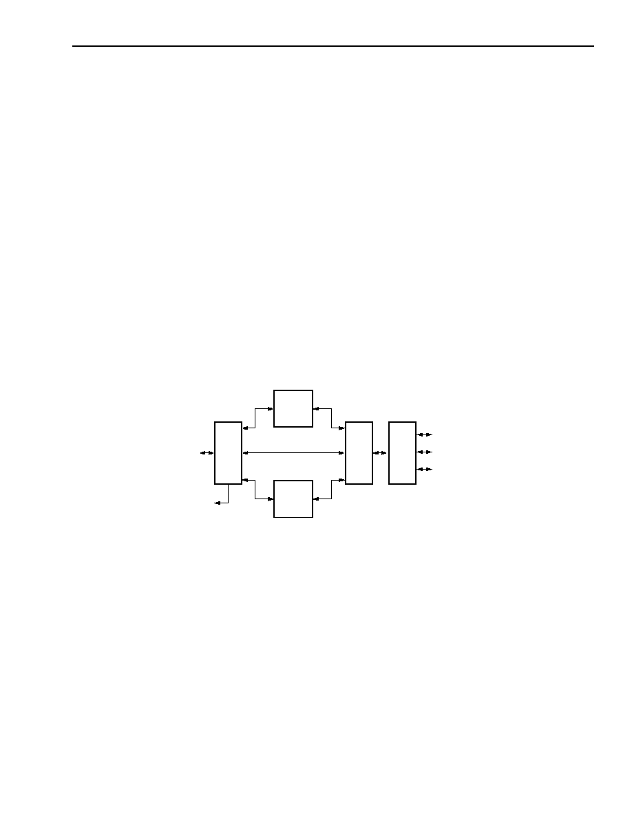
Figure 1. FW323 Functional Block Diagram .............................................................................................................7
Figure 2. PHY Core Block Diagram ........................................................................................................................ 12
Figure 3. Pin Assignments for FW323 .................................................................................................................... 13
Figure 4. Application Schematic for FW323 ........................................................................................................... 19
Figure 5. Bus Timing ............................................................................................................................................ 142
Figure 6. Write Cycle Timing ................................................................................................................................ 142
Figure 7. Data Validity .......................................................................................................................................... 142
Figure 8. Start and Stop Definition ....................................................................................................................... 143
Figure 9. Output Acknowledge ............................................................................................................................. 143

4
4
Agere Systems Inc.
FW323 05
Data Sheet, Rev. 2
1394A PCI PHY/Link Open Host Controller Interface
October 2001
Table of Contents
(continued)
Table
Page
Table 1. Pin Descriptions ........................................................................................................................................14
Table 2. Bit-Field Access Tag Description ..............................................................................................................20
Table 3. PCI Configuration Register Map ...............................................................................................................20
Table 4. Vendor ID Register ...................................................................................................................................21
Table 5. Device ID Register ....................................................................................................................................22
Table 6. PCI Command Register ............................................................................................................................23
Table 7. PCI Command Register Description .........................................................................................................24
Table 8. PCI Status Register ..................................................................................................................................25
Table 9. Class Code and Revision ID Register .....................................................................................................26
Table 10. Class Code and Revision ID Register Description .................................................................................27
Table 11. Latency Timer and Class Cache Line Size Register ..............................................................................27
Table 12. Latency Timer and Class Cache Line Size Register Description ..........................................................28
Table 13. Header Type and BIST Register ............................................................................................................28
Table 14. Header Type and BIST Register Description .........................................................................................29
Table 15. OHCI Base Address Register .................................................................................................................30
Table 16. OHCI Base Address Register Description ..............................................................................................31
Table 17. PCI Subsystem Identification Register Description ................................................................................32
Table 18. PCI Power Management Capabilities Pointer Register ..........................................................................32
Table 19. Interrupt Line and Pin Register ...............................................................................................................33
Table 20. Interrupt Line and Pin Register Description ............................................................................................33
Table 21. MIN_GNT and MAX_LAT Register .........................................................................................................34
Table 22. MIN_GNT and MAX_LAT Register Description ......................................................................................34
Table 23. PCI OHCI Control Register ....................................................................................................................35
Table 24. PCI OHCI Control Register Description ..................................................................................................36
Table 25. Capability ID and Next Item Pointer Register .........................................................................................37
Table 26. Capability ID and Next Item Pointer Register Description ......................................................................37
Table 27. Power Management Capabilities Register .............................................................................................38
Table 28. Power Management Capabilities Register Description ..........................................................................39
Table 29. Power Management Control and Status Register .................................................................................40
Table 30. Power Management Control and Status Register Description ...............................................................41
Table 31. Power Management Extension Register ................................................................................................42
Table 32. Power Management Extension Register Description ............................................................................42
Table 33. OHCI Register Map ................................................................................................................................43
Table 34. OHCI Version Register ...........................................................................................................................46
Table 35. OHCI Version Register Description ........................................................................................................47
Table 36. GUID ROM Register ..............................................................................................................................48
Table 37. GUID ROM Register Description ............................................................................................................49
Table 38. Asynchronous Transmit Retries Register ..............................................................................................50
Table 39. Asynchronous Transmit Retries Register Description ............................................................................51
Table 40. CSR Data Register .................................................................................................................................52
Table 41. CSR Data Register Description ..............................................................................................................53
Table 42. CSR Compare Register ..........................................................................................................................54
Table 43. CSR Compare Register Description .......................................................................................................55
Table 44. CSR Control Register .............................................................................................................................56
Table 45. CSR Control Register Description .........................................................................................................57
Table 46. Configuration ROM Header Register ......................................................................................................58
Table 47. Configuration ROM Header Register Description ..................................................................................59
Table 48. Bus Identification Register ......................................................................................................................60
Table 49. Bus Identification Register Description ...................................................................................................61
Table 50. Bus Options Register ..............................................................................................................................62
Table 51. Bus Options Register Description ...........................................................................................................63

Agere Systems Inc.
5
Data Sheet, Rev. 2
FW323 05
October 2001
1394A PCI PHY/Link Open Host Controller Interface
Table of Contents
(continued)
Table
Page
Table 52. GUID High Register ................................................................................................................................64
Table 53. GUID High Register Description .............................................................................................................65
Table 54. GUID Low Register .................................................................................................................................66
Table 55. GUID Low Register Description ..............................................................................................................67
Table 56. Configuration ROM Mapping Register ....................................................................................................68
Table 57. Configuration ROM Mapping Register Description .................................................................................69
Table 58. Posted Write Address Low Register .......................................................................................................70
Table 59. Posted Write Address Low Register Description ....................................................................................71
Table 60. Posted Write Address High Register ......................................................................................................72
Table 61. Posted Write Address High Register Description ...................................................................................73
Table 62. Vendor ID Register .................................................................................................................................74
Table 63. Vendor ID Register Description ..............................................................................................................75
Table 64. Host Controller Control Register .............................................................................................................76
Table 65. Host Controller Control Register Description ..........................................................................................77
Table 66. Self-ID Buffer Pointer Register ...............................................................................................................78
Table 67. Self-ID Buffer Pointer Register Description ............................................................................................79
Table 68. Self-ID Count Register ............................................................................................................................80
Table 69. Self-ID Count Register Description .........................................................................................................81
Table 70. Isochronous Receive Channel Mask High Register ...............................................................................82
Table 71. Isochronous Receive Channel Mask High Register Description ............................................................83
Table 72. Isochronous Receive Channel Mask Low Register ................................................................................84
Table 73. Isochronous Receive Channel Mask Low Register Description ............................................................85
Table 74. Interrupt Event Register ..........................................................................................................................86
Table 75. Interrupt Event Register Description .......................................................................................................87
Table 76. Interrupt Mask Register ..........................................................................................................................89
Table 77. Interrupt Mask Register Description .......................................................................................................90
Table 78. Isochronous Transmit Interrupt Event Register ......................................................................................91
Table 79. Isochronous Transmit Interrupt Event Register Description ...................................................................92
Table 80. Isochronous Transmit Interrupt Mask Register .......................................................................................93
Table 81. Isochronous Receive Interrupt Event Register .......................................................................................94
Table 82. Isochronous Receive Interrupt Event Description ..................................................................................95
Table 83. Isochronous Receive Interrupt Mask Register ........................................................................................96
Table 84. Fairness Control Register .......................................................................................................................97
Table 85. Fairness Control Register Description ....................................................................................................98
Table 86. Link Control Register .............................................................................................................................99
Table 87. Link Control Register Description ........................................................................................................100
Table 88. Node Identification Register .................................................................................................................101
Table 89. Node Identification Register Description ..............................................................................................102
Table 90. PHY Core Layer Control Register ........................................................................................................103
Table 91. PHY Core Layer Control Register Description .....................................................................................104
Table 92. Isochronous Cycle Timer Register .......................................................................................................105
Table 93. Isochronous Cycle Timer Register Description ....................................................................................106
Table 94. Asychronous Request Filter High Register ..........................................................................................107
Table 95. Asynchronous Request Filter High Register Description ......................................................................108
Table 96. Asynchronous Request Filter Low Register ........................................................................................110
Table 97. Asynchronous Request Filter Low Register Description ......................................................................111
Table 98. Physical Request Filter High Register ..................................................................................................113
Table 99. Physical Request Filter High Register Description ...............................................................................114
Table 100. Physical Request Filter Low Register ................................................................................................116
Table 101. Physical Request Filter Low Register Description ..............................................................................117
Table 102. Asynchronous Context Control Register ............................................................................................119

6
6
Agere Systems Inc.
FW323 05
Data Sheet, Rev. 2
1394A PCI PHY/Link Open Host Controller Interface
October 2001
Table of Contents
(continued)
Table
Page
Table 103. Asynchronous Context Control Register Description ........................................................................120
Table 104. Asynchronous Context Command Pointer Register ..........................................................................121
Table 105. Asynchronous Context Command Pointer Register Description ........................................................122
Table 106. Isochronous Transmit Context Control Register .................................................................................123
Table 107. Isochronous Transmit Context Control Register Description .............................................................124
Table 108. Isochronous Transmit Context Command Pointer Register ...............................................................125
Table 109. Isochronous Transmit Context Command Pointer Register Description ............................................126
Table 110. Isochronous Receive Context Control Register ..................................................................................127
Table 111. Isochronous Receive Context Control Register Description ...............................................................128
Table 112. Isochronous Receive Context Command Pointer Register ................................................................129
Table 113. Isochronous Receive Context Command Pointer Register Description .............................................130
Table 114. Isochronous Receive Context Match Register ...................................................................................131
Table 115. Isochronous Receive Context Match Register Description ................................................................132
Table 116. FW323 Vendor Specific Registers Description ...................................................................................133
Table 117. Isochronous DMA Control Registers Description ...............................................................................134
Table 118. Asynchronous DMA Control Registers Description ............................................................................135
Table 119. Link Registers Description ..................................................................................................................136
Table 120. ROM Format Description ....................................................................................................................137
Table 121. Absolute Maximum Ratings ................................................................................................................138
Table 122. Analog Characteristics ........................................................................................................................139
Table 123. Driver Characteristics .........................................................................................................................140
Table 124. Device Characteristics ........................................................................................................................140
Table 125. Switching Characteristics ...................................................................................................................141
Table 126. Clock Characteristics ..........................................................................................................................141
Table 127. ac Characteristics of Serial EEPROM Interface Signals ....................................................................141
Table 128. PHY Core Register Map for the Cable Environment ..........................................................................144
Table 129. PHY Core Register Fields for Cable Environment ..............................................................................145
Table 130. PHY Core Register Page 0: Port Status Page ...................................................................................147
Table 131. PHY Core Register Port Status Page Fields .....................................................................................148
Table 132. PHY Core Register Page 1: Vendor Identification Page ....................................................................149
Table 133. PHY Core Register Vendor Identification Page Fields .......................................................................149
Agere Systems Inc.
7
Data Sheet, Rev. 2
FW323 05
October 2001
1394A PCI PHY/Link Open Host Controller Interface
FW323 Functional Overview
s
PCI:
-- Revision 2.2 compliant
-- 33 MHz/32-bit operation
-- Programmable burst size for PCI data transfer
-- Supports PCI Bus Power Management Interface Specification v.1.1
-- Supports clockrun protocol per PCI Mobile Design Guide
-- Global byte swap function
Other Features
s
I
2
C serial ROM interface
s
CMOS process
s
3.3 V operation, 5 V tolerant inputs
s
128-pin TQFP package
The FW323 is the Agere Systems Inc. implementation of a high-performance, PCI bus-based open host controller for
implementation of
IEEE
1394a-2000 compliant systems and devices. Link-layer functions are handled by the
FW323, utilizing the on-chip 1394a-2000 compliant link core and physical layer core. A high-performance and cost-
effective solution for connecting and servicing multiple
IEEE
1394 (both 1394-1995 and 1394a-2000) peripheral
devices can be realized.
5-6250 (F).e
Figure 1. FW323 Functional Block Diagram
PCI
BUS
CABLE PORT 2
PCI
ROM
OHCI
OHCI
LINK
CORE
ISOCH
ASYNC
I/F
CORE
PHY
CORE
CABLE PORT 1
CABLE PORT 0
FW323 Functional Description
The FW323 is comprised of five major functional
sections (see Figure 1): PCI core, isochronous data
transfer, asynchronous data transfer, link core, and
PHY core. The following is a general description of
each of the five major sections.
PCI Core
The PCI core serves as the interface to the PCI bus. It
contains the state machines that allow the FW323 to
respond properly when it is the target of the transaction.
During 1394 packet transmission or reception, the PCI
core arbitrates for the PCI bus and enables the FW323
to become the bus master for reading the different
buffer descriptors and management of the actual data
transfers to/from host system memory.
The PCI core also supports the
PCI Bus Power
Management Interface Specification
v.1.1. Included in
this support is a standard power management register
interface accessible through the PCI configuration
space. Through this register interface, software is able
to transition the FW323 into four distinct power
consumption states (D0, D1, D2, and D3). This permits
software to selectively increase/decrease the power
consumption of the FW323 for reasons such as periods
of system inactivity or power conservation. In addition,
the FW323 also includes support for hardware wake-up
mechanisms through power management events

8
Agere Systems Inc.
FW323 05
Data Sheet, Rev. 2
1394A PCI PHY/Link Open Host Controller Interface
October 2001
FW323 Functional Description
(continued)
(PMEs). When the FW323 is in a low-power state,
PMEs provide a hardware mechanism for requesting a
software wake-up. Together, the power management
register interface and PME support within the FW323
combine to form an efficient means for implementing
power management.
Isochronous Data Transfer
The isochronous data transfer logic handles the transfer
of isochronous data between the link core and the PCI
interface module. It consists of the isochronous register
module, the isochronous transmit DMA module, the
isochronous receive DMA module, the isochronous
transmit FIFO, and the isochronous receive FIFO.
Isochronous Register
The isochronous register module operates on PCI slave
accesses to OHCI registers within the isochronous
block. The module also maintains the status of inter-
rupts generated within the isochronous block and sends
the isochronous interrupt status to the OHCI interrupt
handler block.
Isochronous Transmit DMA (ITDMA)
The isochronous transmit DMA module moves data
from host memory to the link core, which will then send
the data to the 1394 bus. It consists of isochronous
contexts, each of which is independently controlled by
software, and can send data on a 1394 isochronous
channel.
During each 1394 isochronous cycle, the ITDMA
module will service each of the contexts and attempt to
process one 1394 packet for each context. If a context
is active, ITDMA will request access to the PCI bus.
When granted PCI access, a descriptor block is
fetched from host memory. This data is decoded by
ITDMA to determine how much data is required and
where in host memory the data resides. ITDMA
initiates another PCI access to fetch this data, which is
placed into the transmit FIFO for processing by the link
core. If the context is not active, it is skipped by ITDMA
for the current cycle.
After processing each context, ITDMA writes a cycle
marker word in the transmit FIFO to indicate to the link
core that there is no more data for this isochronous
cycle. As a summary, the major steps for the FW323
ITDMA to transmit a packet are the following:
1. Fetch a descriptor block from host memory.
2. Fetch data specified by the descriptor block from
host memory and place it into the isochronous
transmit FIFO.
3. Data in FIFO is read by the link and sent to the PHY
core device interface.
Isochronous Receive DMA (IRDMA)
The isochronous receive DMA module moves data
from the receive FIFO to host memory. It consists of
isochronous contexts, each of which is independently
controlled by software. Normally, each context can
process data on a single 1394 isochronous channel.
However, software can select one context to receive
data on multiple channels.
When IRDMA detects that the link core has placed data
into the receive FIFO, it immediately reads out the first
word in the FIFO, which makes up the header of the
isochronous packet. IRDMA extracts the channel
number for the packet and packet filtering controls from
the header. This information is compared with the
control registers for each context to determine if any
context is to process this packet.
If a match is found, IRDMA will request access to the
PCI bus. When granted PCI access, a descriptor block
is fetched from host memory. The descriptor provides
information about the host memory block allocated for
the incoming packet. IRDMA then reads the packet
from the receive FIFO and writes the data to host
memory via the PCI bus.
If no match is found, IRDMA will read the remainder of
the packet from the receive FIFO, but not process the
data in any way.
Asynchronous Data Transfer
The ASYNC block is functionally partitioned into two
independent logic blocks for transmitting and receiving
1394 packets. The ASYNC_TX unit is responsible for
packet transmission while the ASYNC_RX unit pro-
cesses received data.
Asynchronous Register
The asynchronous register module operates on PCI
slave accesses to OHCI registers within the asynchro-
nous block. The module also maintains the status of
interrupts generated within the asynchronous block
and sends the asynchronous interrupt status to the
OHCI interrupt handler block.

Agere Systems Inc.
9
Data Sheet, Rev. 2
FW323 05
October 2001
1394A PCI PHY/Link Open Host Controller Interface
FW323 Functional Description
(continued)
Asynchronous Transmit (ASYNC_TX)
The ASYNC_TX block of the FW323 manages the
asynchronous transmission of either request or
response packets. The mechanism for asynchronous
transmission of requests and responses are similar.
The only difference is the system memory location of
the buffer descriptor list when processing the two
contexts. Therefore, the discussion below, which is for
asynchronous transmit requests, parallels that of the
asynchronous transmit response. The FW323 asyn-
chronous transmission of packets involves the following
steps:
1. Fetch complete buffer descriptor block from host
memory.
2. Get data from system memory and store into
async FIFO.
3. Request transfer of data from FIFO to link device.
4. Handle retries, if any.
5. Handle errors in steps 1 to 4.
6. End the transfer if there are no errors.
Asynchronous Receive (ASYNC_RX)
The ASYNC_RX block of the FW323 manages the
processing of received packets. Data packets are
parsed and stored in a dedicated asynchronous
receive FIFO. Command descriptors are read through
the PCI interface to determine the disposition of the
data arriving through the 1394 link.
The header of the received packet is processed to
determine, among other things, the following:
1. The type of packet received.
2. The source and destinations.
3. The data and size, if any.
4. The operation required, if any. For example, com-
pare and swap operation.
The ASYNC block also handles DMA transfers of self-
ID packets during the 1394 bus initialization phase and
block transactions associated with physical request.
Serial EEPROM Interface
The FW323 features an I
2
C
compliant serial ROM
interface that allows for the connection of an external
serial EEPROM. The interface provides a mechanism
to store configuable data such as the global unique
identification (GUID) within an external EEPROM. The
interface consists of the ROM_AD and ROM_CLK pins.
ROM_CLK is an output clock provided by the FW323 to
the external EEPROM. ROM_AD is bidirectional and is
used for serial data/control transfer between the FW323
and the external EEPROM. The FW323 uses this
interface to read the contents of the serial EEPROM
during initial power-up or when a hardware reset
occurs. The FW323 also makes the serial ROM
interface visible to software through the OHCI defined
GUID ROM register. When the FW323 is operational,
the GUID ROM register allows software to initiate reads
to the external EEPROM.
Link Core
It is the responsibility of the link to ascertain if a
received packet is to be forwarded to the OHCI for
processing. If so, the packet is directed to a proper
inbound FIFO for either the isochronous block or the
asynchronous block to process. The link is also
responsible for CRC generation on outgoing packets
and CRC checking on receiving packets.
To become aware of data to be sent outbound on 1394
bus, the link must monitor the OHCI FIFOs looking for
packets in need of transmission. Based on data
received from the OHCI block, the link will form packet
headers for the 1394 bus. The link will alert the PHY
core as to the availability of the outbound data. It is the
link's function to generate CRC for the outbound data.
The link also provides PHY core register access for the
OHCI.
PHY Core
The PHY core provides the analog physical layer func-
tions needed to implement a three-port node in a
cable-based
IEEE
1394-1995 and
IEEE
1394a-2000
network.
Each cable port incorporates two differential line trans-
ceivers. The transceivers include circuitry to monitor
the line conditions as needed for determining connec-
tion status, for initialization and arbitration, and for
packet reception and transmission. The PHY core
interfaces with the link core.
The PHY core requires either an external 24.576 MHz
crystal or crystal oscillator. The internal oscillator
drives an internal phase-locked loop (PLL), which gen-
erates the required 400 MHz reference signal. The
400 MHz reference signal is internally divided to pro-
vide the 49.152 MHz, 98.304 MHz, and 196.608 MHz
clock signals that control transmission of the outbound
clock signal is also supplied to the associated LLC for
synchronization of the two chips and is used for resyn-
chronization of the received data.

10
Agere Systems Inc.
FW323 05
Data Sheet, Rev. 2
1394A PCI PHY/Link Open Host Controller Interface
October 2001
FW323 Functional Description
(continued)
The PHY/link interface is a direct connection and does
not provide isolation.
Data bits to be transmitted through the cable ports are
received from the LLC on two, four, or eight data lines
(D[0:7]), and are latched internally in the PHY in syn-
chronization with the 49.152 MHz system clock. These
bits are combined serially, encoded, and transmitted at
98.304 Mbits/s, 196.608 Mbits/s, or 393.216 Mbits/s as
the outbound data-strobe information stream. During
transmission, the encoded data information is transmit-
ted differentially on the TPA and TPB cable pair(s).
During packet reception, the TPA and TPB transmit-
ters of the receiving cable port are disabled, and the
receivers for that port are enabled. The encoded data
information is received on the TPA and TPB cable
pair. The received data-strobe information is decoded
to recover the receive clock signal and the serial data
bits. The serial data bits are split into two, four, or eight
parallel streams, resynchronized to the local system
clock, and sent to the associated LLC. The received
data is also transmitted (repeated) out of the other
active (connected) cable ports.
Both the TPA and TPB cable interfaces incorporate
differential comparators to monitor the line states
during initialization and arbitration. The outputs of
these comparators are used by the internal logic to
determine the arbitration status. The TPA channel
monitors the incoming cable common-mode voltage.
The value of this common-mode voltage is used during
arbitration to set the speed of the next packet
transmission. In addition, the TPB channel monitors
the incoming cable common-mode voltage for the
presence of the remotely supplied twisted-pair bias
voltage. This monitor is called bias-detect.
The TPBIAS circuit monitors the value of incoming
TPA pair common-mode voltage when local TPBIAS is
inactive. Because this circuit has an internal current
source and the connected node has a current sink, the
monitored value indicates the cable connection status.
The monitor is called connect-detect.
Both the TPB bias-detect monitor and TPBIAS
connect-detect monitor are used in suspend/resume
signaling and cable connection detection.
The PHY core provides a 1.86 V nominal bias voltage
for driver load termination. This bias voltage, when
seen through a cable by a remote receiver, indicates
the presence of an active connection. The value of this
bias voltage has been chosen to allow interoperability
between transceiver chips operating from 5 V or 3 V
nominal supplies. This bias voltage source should be
stabilized by using an external filter capacitor of
approximately 0.33 µF.
The port transmitter circuitry and the receiver circuitry
are disabled when the port is disabled, suspended, or
disconnected.
The line drivers in the PHY core operate in a high-
impedance current mode and are designed to work
with external 112
line-termination resistor networks.
One network is provided at each end of each twisted
pair cable. Each network is composed of a pair of
series-connected 56
resistors. The midpoint of the
pair of resistors that is directly connected to the
twisted pair A (TPA) signals is connected to the
TPBIAS voltage signal. The midpoint of the pair of
resistors that is directly connected to the twisted-pair B
(TPB) signals is coupled to ground through a parallel
RC network with recommended resistor and capacitor
values of 5 k
and 220 pF, respectively. The value of
the external resistors are specified to meet the draft
standard specifications when connected in parallel
with the internal receiver circuits.
The driver output current, along with other internal
operating currents, is set by an external resistor. This
resistor is connected between the R0 and R1 signals
and has a value of 2.49
k
±1%.
Four signals are used as inputs to set four
configuration status bits in the self-identification (self-
ID) packet. These signals are hardwired high or low as
a function of the equipment design. PC[0:2] are the
three signals that indicate either the need for power
from the cable or the ability to supply power to the
cable. The fourth signal (CONTENDER), as an input,
indicates whether a node is a contender for bus
manager. When the CONTENDER signal is asserted,
it means the node is a contender for bus manager.
When the signal is not asserted, it means that the
node is not a contender. The contender bit
corresponds to bit 20 in the self-ID packet, PC0
corresponds to bit 21, PC1 corresponds to bit 22, and
PC2 corresponds to bit 23 (see Table 4-29 of the
IEEE
1394-1995 standard for additional details).
When the power supply of the PHY core is removed
while the twisted-pair cables are connected, the PHY
core transmitter and receiver circuitry has been
designed to present a high impedance to the cable in
order to not load the TPBIAS signal voltage on the
other end of the cable.
For reliable operation, the TPB± signals must be
terminated using the normal termination network,

Agere Systems Inc.
11
Data Sheet, Rev. 2
FW323 05
October 2001
1394A PCI PHY/Link Open Host Controller Interface
FW323 Functional Description
(continued)
regardless of whether a cable is connected to port or
not connected to a port. For those applications, when
FW323 is used with one or more of the ports not
brought out to a connector, those unused ports may be
left unconnected without normal termination. When a
port does not have a cable connected, internal
connect-detect circuitry will keep the port in a
disconnected state.
Note: All gap counts on all nodes of a 1394 bus must
be identical. This may be accomplished by using
PHY core configuration packets (see Section
4.3.4.3 of
IEEE
1394-1995 standard) or by using
two bus resets, which resets the gap counts to
the maximum level (3Fh).
The internal link power status (LPS) signal works with
the internal LinkOn signal to manage the LLC power
usage of the node. The LPS signal indicates that the
LLC of the node is powered up or down. If LPS is
inactive for more than 1.2 µs and less than 25 µs, the
internal PHY/link interface is reset.
If LPS is inactive for greater than 25 µs, the PHY will
disable the internal PHY/link interface to save power.
The FW323 continues its repeater function. If the PHY
then receives a link-on packet, the internal LinkOn sig-
nal is activated to output a 6.114 MHz signal, which can
be used by the LLC to power itself up. Once the LLC is
powered up, the internal LPS signal communicates this
to the PHY and the internal PHY/link interface is
enabled. Internal LinkOn signal is turned off when LCtrl
bit is set.
Three of the signals are used to set up various test
conditions used in manufacturing. These signals (SE,
SM, and PTEST) should be connected to V
SS
for
normal operation.
12
12
Agere Systems Inc.
FW323 05
Data Sheet, Rev. 2
1394A PCI PHY/Link Open Host Controller Interface
October 2001
FW323 Functional Description
(continued)
5-5459.i(F) R.01
Figure 2. The PHY Core Block Diagram
LINK
INTERFACE
I/O
RECEIVED
DATA
DECODER/
ARBITRATION
AND
CONTROL
RETIMER
STATE
MACHINE
LOGIC
BIAS
VOLTAGE
AND
CURRENT
GENERATOR
CABLE PORT 1
CABLE PORT 2
OSCILLATOR,
PLL SYSTEM,
AND
CLOCK
GENERATOR
TRANSMIT
DATA
ENCODER
CABLE PORT 0
TPA0+
TPA0≠
TPB0+
TPB0≠
R0
TPBIAS2
R1
TPBIAS0
TPBIAS1
TPA1+
TPA1≠
TPB1+
TPB1≠
TPA2+
TPA2≠
TPB2+
TPB2≠
XI
XO
CPS
LPS
SYSCLK
LREQ
CTL0
CTL1
D0
D1
D2
D3
CONTENDER
SE
SM
RESETN
CRYSTAL
D4
D5
D6
D7
PC0
PC1
PC2
LINKON
Agere Systems Inc.
13
Data Sheet, Rev. 2
FW323 05
October 2001
1394A PCI PHY/Link Open Host Controller Interface
Pin Information
5-7838 (F)a
Note: Active-low signals within this document are indicated by an N following the symbol names.
Figure 3. Pin Assignments for the FW323
1
2
3
4
5
6
7
8
9
10
11
12
13
14
15
16
17
18
19
20
21
22
23
24
25
26
27
28
29
30
31
32
33
34
35
36
37
38
VDD
VSS
CARDBUSN
NC
CNA
NANDTREE
TEST1
ROM_CLK
ROM_AD
TEST0
VDD
VSS
CLKRUNN
PCI_INTAN
PCI_RSTN
PCI_GNTN
PCI_REQN
PCI_PMEN
VDD
PCI_CLK
VSS
PCI_AD[31]
PCI_AD[30]
PCI_AD[29]
PCI_AD[28]
VDD
VSS
PCI_AD[27]
PCI_AD[26]
PCI_AD[25]
PCI_AD[24]
VSS
PCI_CBEN[3]
PCI_IDSEL
PCI_AD[23]
PCI_AD[22]
VDD
VSS
39
40
41
42
43
44
45
46
47
48
49
50
51
52
53
54
55
56
57
58
59
60
61
62
63
64
P
C
I_A
D
[21]
P
C
I_A
D
[20]
P
C
I_A
D
[18]
VD
D
VS
S
P
C
I_A
D
[17]
P
C
I_A
D
[16]
PC
I
_
C
B
EN
[
2
]
P
C
I
_
F
R
AM
EN
VD
D
VS
S
P
C
I_IRDY
N
P
C
I_
T
RDY
N
PC
I
_
D
E
V
SEL
N
PC
I
_
S
T
O
P
N
VD
D
VS
S
P
C
I_
P
E
RRN
P
C
I_
S
E
RRN
P
C
I
_
PAR
PC
I
_
C
B
EN
[
1
]
VS
S
P
C
I_A
D
[15]
P
C
I_A
D
[14]
P
C
I_A
D
[13]
PCI_AD[12]
VSS
PCI_AD[11]
PCI_AD[10]
PCI_AD[9]
PCI_AD[8]
VSS
VDD
PCI_CBEN[0]
PCI_AD[7]
PCI_AD[6]
PCI_AD[5]
VSS
PCI_AD[4]
PCI_AD[3]
PCI_AD[2]
VSS
VDD
PCI_AD[1]
PCI_AD[0]
PCI_VIOS
CONTENDER
PC2
PC1
PC0
LKON
LPS
NC
VDD
CPS
VSSA
VDDA
TPB2≠
TPB2+
TPA2≠
TPA2+
TPBIAS2
VSSA
65
66
67
68
69
70
71
72
73
74
75
76
77
78
79
80
81
82
83
84
85
86
87
88
89
90
91
92
93
94
95
96
97
98
99
100
101
102
103
105
106
107
108
109
110
111
112
113
114
115
116
117
118
119
120
121
122
123
124
125
126
127
128
VS
SA
V
DDA
TP
B
1
≠
TP
B
1
+
TP
A
1
≠
TP
A
1
+
T
P
B
I
AS1
TP
B
0
+
TP
A
0
≠
TP
A
0
+
T
P
B
I
AS0
VS
SA
V
DDA
R0
R1
PL
L
V
D
D
PL
L
VSS
XI
XO
RE
S
E
T
N
PT
E
S
T
SM
SE
NC
NC
104
TP
B
0
≠
P
C
I_A
D
[19]

14
14
Agere Systems Inc.
FW323 05
Data Sheet, Rev. 2
1394A PCI PHY/Link Open Host Controller Interface
October 2001
Pin Information
(continued)
Table 1. Pin Descriptions
Pin
Symbol*
* Active-low signals within this document are indicated by an N following the symbol names.
Type
Description
1
VDD
--
Power.
2
VSS
--
Ground.
3
CARDBUSN
I
CardBusN (Active-Low). Selects mode of operation for
PCI output buffers. Tie low for cardbus operation, high
for PCI operation. An internal pull-up is provided to force
buffers to PCI mode, if no connection is made to this
pin.
4
NC
--
No Connect.
5
CNA
O
Cable Not Active. CNA output is provided for use in
legacy power management systems.
6
NANDTREE
O
Nand Tree Test Output. When the chip is placed into
the NAND tree test mode, the pin is the output of the
NAND tree logic. This pin is not used during functional
operation.
7
TEST1
I
Test. Used for device testing. Tie to VSS.
8
ROM_CLK
I/O
ROM Clock.
9
ROM_AD
I/O
ROM Address/Data.
10
TEST0
I
Test. Used for device testing. Tie to VSS.
11
VDD
--
Power.
12
VSS
--
Ground.
13
CLKRUNN
I/O
CLKRUNN (Active-Low). Optional signal for PCI
mobile environment. If not used, CLKRUNN pin needs
to be pulled down to VSS for correct operation.
14
PCI_INTAN
O
PCI Interrupt (Active-Low).
15
PCI_RSTN
I
PCI Reset (Active-Low).
16
PCI_GNTN
I
PCI Grant Signal (Active-Low).
17
PCI_REQN
O
PCI Request Signal (Active-Low).
18
PCI_PMEN
O
PCI Power Management Event (Active-Low).
19
VDD
--
Power.
20
PCI_CLK
I
PCI Clock Input. 33 MHz.
21
VSS
--
Ground.
22
PCI_AD[31]
I/O
PCI Address/Data Bit.
23
PCI_AD[30]
I/O
PCI Address/Data Bit.
24
PCI_AD[29]
I/O
PCI Address/Data Bit.
25
PCI_AD[28]
I/O
PCI Address/Data Bit.
26
VDD
--
Power.
27
VSS
--
Ground.
28
PCI_AD[27]
I/O
PCI Address/Data Bit.
29
PCI_AD[26]
I/O
PCI Address/Data Bit.
30
PCI_AD[25]
I/O
PCI Address/Data Bit.
31
PCI_AD[24]
I/O
PCI Address/Data Bit.
32
VSS
--
Ground.
33
PCI_CBEN[3]
I/O
PCI Command/Byte Enable (Active-Low).
34
PCI_IDSEL
I
PCI ID Select.
35
PCI_AD[23]
I/O
PCI Address/Data Bit.

Agere Systems Inc.
15
Data Sheet, Rev. 2
FW323 05
October 2001
1394A PCI PHY/Link Open Host Controller Interface
Pin Information
(continued)
Table 1. Pin Descriptions (continued)
Pin
Symbol*
* Active-low signals within this document are indicated by an N following the symbol names.
Type
Description
36
PCI_AD[22]
I/O
PCI Address/Data Bit.
37
V
DD
--
Power.
38
V
SS
--
Ground.
39
PCI_AD[21]
I/O
PCI Address/Data Bit.
40
PCI_AD[20]
I/O
PCI Address/Data Bit.
41
PCI_AD[19]
I/O
PCI Address/Data Bit.
42
PCI_AD[18]
I/O
PCI Address/Data Bit.
43
V
DD
--
Power.
44
V
SS
--
Ground.
45
PCI_AD[17]
I/O
PCI Address/Data Bit.
46
PCI_AD[16]
I/O
PCI Address/Data Bit.
47
PCI_CBEN[2]
I/O
PCI Command/Byte Enable Signal (Active-Low).
48
PCI_FRAMEN
I/O
PCI Frame Signal (Active-Low).
49
V
DD
--
Power.
50
V
SS
--
Ground.
51
PCI_IRDYN
I/O
PCI Initiator Ready Signal (Active-Low).
52
PCI_TRDYN
I/O
PCI Target Ready Signal (Active-Low).
53
PCI_DEVSELN
I/O
PCI Device Select Signal (Active-Low).
54
PCI_STOPN
I/O
PCI Stop Signal (Active-Low).
55
V
DD
--
Power.
56
V
SS
--
Ground.
57
PCI_PERRN
I/O
PCI Parity Error Signal (Active-Low).
58
PCI_SERRN
I/O
PCI System Error Signal (Active-Low).
59
PCI_PAR
I/O
PCI Parity Signal.
60
PCI_CBEN[1]
I/O
PCI Command/Byte Enable Signal (Active-Low).
61
V
SS
--
Ground.
62
PCI_AD[15]
I/O
PCI Address/Data Bit.
63
PCI_AD[14]
I/O
PCI Address/Data Bit.
64
PCI_AD[13]
I/O
PCI Address/Data Bit.
65
PCI_AD[12]
I/O
PCI Address/Data Bit.
66
V
SS
--
Ground.
67
PCI_AD[11]
I/O
PCI Address/Data Bit.
68
PCI_AD[10]
I/O
PCI Address/Data Bit.
69
PCI_AD[9]
I/O
PCI Address/Data Bit.
70
PCI_AD[8]
I/O
PCI Address/Data Bit.
71
V
SS
--
Ground.
72
V
DD
--
Power.
73
PCI_CBEN[0]
I/O
PCI Command/Byte Enable Signal (Active-Low).
74
PCI_AD[7]
I/O
PCI Address/Data Bit.
75
PCI_AD[6]
I/O
PCI Address/Data Bit.
76
PCI_AD[5]
I/O
PCI Address/Data Bit.
77
V
SS
--
Ground.
78
PCI_AD[4]
I/O
PCI Address/Data Bit.

16
16
Agere Systems Inc.
FW323 05
Data Sheet, Rev. 2
1394A PCI PHY/Link Open Host Controller Interface
October 2001
Pin Information
(continued)
Table 1. Pin Descriptions (continued)
Pin
Symbol*
* Active-low signals within this document are indicated by an N following the symbol names.
Type
Description
79
PCI_AD[3]
I/O
PCI Address/Data Bit.
80
PCI_AD[2]
I/O
PCI Address/Data Bit.
81
V
SS
--
Ground.
82
V
DD
--
Power.
83
PCI_AD[1]
I/O
PCI Address/Data Bit.
84
PCI_AD[0]
I/O
PCI Address/Data Bit.
85
PCI_VIOS
--
PCI Signaling Indicator. (5 V or 3.3 V.)
86
CONTENDER
I
Contender. On hardware reset, this input sets the
default value of the CONTENDER bit indicated during
self-ID. This bit can be programmed by tying the signal
to V
DD
(high) or to ground (low).
87
PC2
I
Power-Class Indicators. On hardware reset, these
inputs set the default value of the power class indicated
during self-ID. These bits can be programmed by tying
the signals to V
DD
(high) or to ground (low).
88
PC1
89
PC0
90
LKON
O
Link On. Signal from the internal PHY core to the
internal link core. This signal is provided as an output
for use in legacy power management systems.
91
LPS
O
Link Power Status. Signal from the internal link core to
the internal PHY core. LPS is provided as an output for
use in legacy power management systems.
92
NC
--
No Connect.
93
V
DD
--
Power.
94
CPS
I
Cable Power Status. CPS is normally connected to the
cable power through a 400 k
resistor. This circuit
drives an internal comparator that detects the presence
of cable power. This information is maintained in one
internal register and is available to the LLC by way of a
register read (see
IEEE
1394a-2000,
Standard for a
High Performance Serial Bus
(Supplement)).
95
V
SSA
--
Analog Circuit Ground. All V
SSA
signals should be
tied together to a low-impedance ground plane.
96
V
DDA
--
Analog Circuit Power. V
DDA
supplies power to the
analog portion of the device.
97
TPB2-
Analog I/O
Port 2, Port Cable Pair B. TPB2± is the port B connec-
tion to the twisted-pair cable. Board traces from each
pair of positive and negative differential signal pins
should be kept matched and as short as possible to the
external load resistors and to the cable connector.
98
TPB2+
99
TPA2-
Analog I/O
Port 2, Port Cable Pair A. TPA2± is the port A connec-
tion to the twisted-pair cable. Board traces from each
pair of positive and negative differential signal pins
should be kept matched and as short as possible to the
external load resistors and to the cable connector.
100
TPA2+

Agere Systems Inc.
17
Data Sheet, Rev. 2
FW323 05
October 2001
1394A PCI PHY/Link Open Host Controller Interface
Pin Information
(continued)
Table 1. Pin Descriptions (continued)
Pin
Symbol*
* Active-low signals within this document are indicated by an N following the symbol names.
Type
Description
101
TPBIAS2
Analog I/O
Port 2, Twisted-Pair Bias. TPBIAS2 provides the
1.86 V nominal bias voltage needed for proper opera-
tion of the twisted-pair cable drivers and receivers and
for sending a valid cable connection signal to the
remote nodes.
102
V
SSA
--
Analog Circuit Ground. All V
SSA
signals should be
tied together to a low-impedance ground plane.
103
V
SSA
--
Analog Circuit Ground. All V
SSA
signals should be
tied together to a low-impedance ground plane.
104
V
DDA
--
Analog Circuit Ground. V
DDA
supplies power to the
analog portion of the device.
105
TPB1≠
Analog I/O
Port 1, Port Cable Pair B. TPB1± is the port B connec-
tion to the twisted-pair cable. Board traces from each
pair of positive and negative differential signal pins
should be kept matched and as short as possible to the
external load resistors and to the cable connector.
106
TPB1+
107
TPA1≠
Analog I/O
Port 1, Port Cable Pair A. TPA1± is the port A connec-
tion to the twisted-pair cable. Board traces from each
pair of positive and negative differential signal pins
should be kept matched and as short as possible to the
external load resistors and to the cable connector.
108
TPA1+
109
TPBIAS1
Analog I/O
Port 1, Twisted-Pair Bias. TPBIAS1 provides the
1.86 V nominal bias voltage needed for proper opera-
tion of the twisted-pair cable drivers and receivers and
for sending a valid cable connection signal to the
remote nodes.
110
TPB0≠
Analog I/O
Port 0, Port Cable Pair B. TPB0± is the port B connec-
tion to the twisted-pair cable. Board traces from each
pair of positive and negative differential signal pins
should be kept matched and as short as possible to the
external load resistors and to the cable connector.
111
TPB0+
112
TPA0≠
Analog I/O
Port 0, Port Cable Pair A. TPA0± is the port A connec-
tion to the twisted-pair cable. Board traces from each
pair of positive and negative differential signal pins
should be kept matched and as short as possible to the
external load resistors and to the cable connector.
113
TPA0+
114
TPBIAS0
Analog I/O
Port 0, Twisted-Pair Bias. TPBIAS0 provides the
1.86 V nominal bias voltage needed for proper opera-
tion of the twisted-pair cable drivers and receivers and
for sending a valid cable connection signal to the
remote nodes.
115
V
SSA
--
Analog Circuit Ground. All V
SSA
signals should be
tied together to a low-impedance ground plane.
116
V
DDA
--
Analog Circuit Power. V
DDA
supplies power to the
analog portion of the device.

18
18
Agere Systems Inc.
FW323 05
Data Sheet, Rev. 2
1394A PCI PHY/Link Open Host Controller Interface
October 2001
Pin Information
(continued)
Table 1. Pin Descriptions (continued)
Application Schematic
The application schematic presents a complete three-port, 400 Mbits/s
IEEE
1394a-2000 design, featuring the
Agere FW323 PCI bus-based host OHCI controller and 400 Mbits/s PHY core. The FW323 device needs only a
power source (U3), connection to PCI interface, 1394a-2000 terminators and connectors, crystal, and serial
EEPROM. No external PHY is required because the FW323 contains both host controller and PHY core functions.
This design is a secondary (Class 4) power provider to the 1394 bus, and will participate in the required 1394a-
2000 bus activities, even when power on the PCI bus is not energized.
Pin
Symbol*
* Active-low signals within this document are indicated by an N following the symbol names.
Type
Description
117
R0
I
Current Setting Resistor. An internal reference
voltage is applied to a resistor connected between R0
and R1 to set the operating current and the cable driver
output current. A low temperature-coefficient resistor
(TCR) with a value of 2.49 k
± 1% should be used to
meet the
IEEE
1394-1995 standard requirements for
output voltage limits.
118
R1
119
PLLV
DD
--
Power for PLL Circuit. PLLV
DD
supplies power to the
PLL circuitry portion of the device.
120
PLLV
SS
--
Ground for PLL Circuit. PLLV
SS
is tied to a low-
impedance ground plane.
121
XI
--
Crystal Oscillator. XI and XO connect to a
24.576 MHz parallel resonant fundamental mode
crystal. Although when a 24.576 MHz clock source is
used, it can be connected to XI with XO left uncon-
nected. The optimum values for the external shunt
capacitors are dependent on the specifications of the
crystal used. The suggested values of 12 pF are appro-
priate for crystal with 7 pF specified loads. For more
details, see the Crystal Selection Considerations
section.
122
XO
123
RESETN
I
Reset (Active-Low). When RESETN is asserted low
(active), a bus reset condition is set on the active cable
ports and the internal PHY core logic is reset to the
reset start state. An internal pull-up resistor, which is
connected to V
DD
, is provided, so only an external
delay capacitor and resistor are required. This input is a
standard logic buffer and can also be driven by an
open-drain logic output buffer.
124
PTEST
I
Test. Used for device testing. Tie to V
SS
.
125
SM
I
Test Mode Control. SM is used during the manufac-
turing test and should be tied to V
SS
.
126
SE
I
Test Mode Control. SE is used during the manufac-
turing test and should be tied to V
SS
.
127
NC
--
No Connect.
128
NC
--
No Connect.
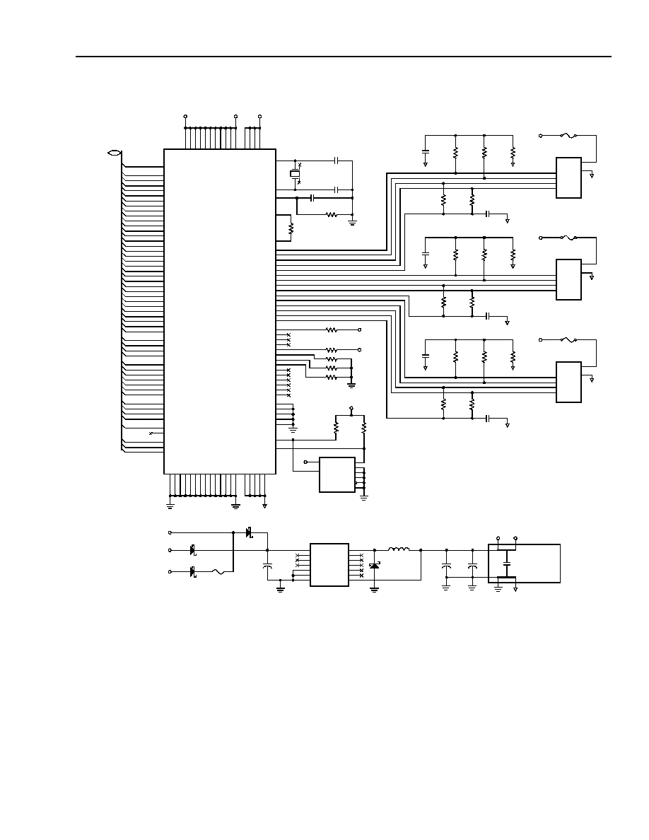
Agere Systems Inc.
19
Data Sheet, Rev. 2
FW323 05
October 2001
1394A PCI PHY/Link Open Host Controller Interface
Application Schematic
(continued)
5-8886(f) R.05fm
Figure 4. Application Schematic for the FW323
AD0
AD1
AD2
AD3
AD4
AD5
AD6
AD7
AD8
AD9
AD10
AD11
AD12
AD13
AD14
AD15
AD16
AD17
AD18
AD19
AD20
AD21
AD22
AD23
AD24
AD25
AD26
AD27
AD28
AD29
AD30
AD31
85
84
83
80
79
78
76
75
74
70
69
68
67
65
64
63
62
46
45
42
41
40
39
36
35
31
30
29
28
25
24
23
22
C_BE#0
73
60
47
33
C_BE#1
C_BE#2
C_BE#3
PAR
FRAME#
IRDY#
TRDY#
DEVSEL#
STOP#
IDSEL
59
48
51
52
53
54
34
17
16
57
58
20
13
15
14
18
REQ#
PERR#
GNT#
SERR#
CLK
RST#
INTA#
PME#
PCI_VIOS
PCI_AD0
PCI_AD1
PCI_AD2
PCI_AD3
PCI_AD4
PCI_AD5
PCI_AD6
PCI_AD7
PCI_AD8
PCI_AD9
PCI_AD10
PCI_AD11
PCI_AD12
PCI_AD13
PCI_AD14
PCI_AD15
PCI_AD16
PCI_AD17
PCI_AD18
PCI_AD19
PCI_AD20
PCI_AD21
PCI_AD22
PCI_AD23
PCI_AD24
PCI_AD25
PCI_AD26
PCI_AD27
PCI_AD28
PCI_AD29
PCI_AD30
PCI_AD31
PCI_CBEN0
PCI_CBEN1
PCI_CBEN2
PCI_CBEN3
PCI_PAR
PCI_FRAMEN
PCI_IRDYN
PCI_TRDYN
PCI_DEVSELN
PCI_STOPN
PCI_IDSEL
PCI_REQN
PCI_GNTN
PCI_PERRN
PCI_SERRN
PCI_PCLK
PCI_CLKRUNN
PCI_PRSTN
PCI_INTAN
PCI_PMEN
93
82
72
55
49
43
37
26
19
11
1
96
10
4
11
6
11
9
VD
D
VD
D
VD
D
VD
D
VD
D
VD
D
VD
D
VD
D
VD
D
VD
D
VD
D
V
DDA
V
DDA
V
DDA
PL
L
V
D
D
TPB0≠
TPB0+
TPA0≠
TPA0+
TPBIAS0
TPB1≠
TPB1+
TPA1≠
TPA1+
TPBIAS1
TPB2≠
TPB2+
TPA2≠
TPA2+
TPBIAS2
111
110
112
113
114
105
106
107
108
109
97
98
99
100
101
CPS
NC
LPS
LKON
PC0
PC1
PC2
CONTENDER
NC
NC
CARDBUSN
NC
CNA
NANDTREE
TEST0
TEST1
PTEST
SE
SM
94
92
91
90
89
88
87
86
128
127
3
4
5
6
10
7
124
126
125
VCC
SDATA
SCLK
A0
A1
A2
WP
GND
AT24C02AN-2.7
VSS
VSS
VSS
VSS
VSS
VSS
VSS
VSS
VSS
VSS
VSS
VSS
VSS
VSS
P
LLV
S
S
VSSA
VSSA
VSSA
VSSA
ROM_AD
ROM_CLK
9
8
X1
X0
RESETN
R1
R0
PCI BUS
FW323
3.3 V
3.3 V
3.3 VA
121
122
123
118
117
C3
Y1
24.576 MHz
C4
C5
R7
2.49 k
1%
1/10 W
1
4
3
2
R13 402 k
1%
R14 10 k
R18 10 k
R19 10 k
R20 10 k
BPWR
3.3 V
3.3 V
R24
R23
10 k
10 k
ROM_AD
ROM_CLK
3.3 V
U2
VOUT
NC
NC
NC
NC
NC
FB
VIN
NC
NC
NC
ON/OFF
SIGGND
PWRGND
AGND
2
12
21
27
32
38
44
50
56
61
66
71
77
81
12
0
11
5
10
3
10
2
95
BPWR
5 V PCI
12 V PCI
CR2
MBRS340T3
CR4
MBRS340T3
F4
1.5 A RESETTABLE
EEPROM
CR1
MBRS340T3
+
C12
22
µ
F
50 V
PWRSRC
10
1
2
7
5
4
6
VP
VG
TPB≠
TPB+
TPA≠
TPA+
AGND
1
2
3
4
5
6
C9
220 pF
R15
56.2
1%
1/10 W
R16
56.2
1%
1/10 W
R17
4.99
1%
1/10 W
J3
1394A PORT 3
AGND
AGND
C11
0.33
µ
F
F3
OMNI-BLOCK FUSE
BPWR
AGND
R21
56.2
1%
1/10 W
R22
56.2
1%
1/10 W
VP
VG
TPB≠
TPB+
TPA≠
TPA+
AGND
1
2
3
4
5
6
C7
220 pF
R8
56.2
1%
1/10 W
R9
56.2
1%
1/10 W
R10
4.99
1%
1/10 W
J2
1394A PORT 2
AGND
AGND
C8
0.33
µ
F
F2
OMNI-BLOCK FUSE
BPWR
AGND
R11
56.2
1%
1/10 W
R12
56.2
1%
1/10 W
VP
VG
TPB≠
TPB+
TPA≠
TPA+
AGND
1
2
3
4
5
6
C1
220 pF
R1
56.2
1%
1/10 W
R2
56.2
1%
1/10 W
R3
4.99
1%
1/10 W
J1
1394A PORT 1
AGND
AGND
C6
0.33
µ
F
F1
OMNI-BLOCK FUSE
BPWR
AGND
R4
56.2
1%
1/10 W
R5
56.2
1%
1/10 W
U3 SUPPLIES VDDX POWER; IT IS SOURCED
BY THE MOST POSITIVE OF PCI 5 V, PCI 12 V,
U3
POWER PLANE
FILTERING
GROUND PLANE
C13
100
µ
F
10 V
C14
100
µ
F
10 V
CR3
MBRS1100T3
L1
680
µ
H
+
+
AGND
3.3 V
3.3 VA
LM2574HVM-3.3
0.1
µ
F
12 pF
12 pF
U1
AND 1394 BUS POWER (BPWR).
8
5
6
1
2
3
7
4
12
8
9
11
13
14
3
510 k

20
20
Agere Systems Inc.
FW323 05
Data Sheet, Rev. 2
1394A PCI PHY/Link Open Host Controller Interface
October 2001
Internal Registers
This section describes the internal registers in FW323, including both PCI configuration registers and OHCI regis-
ters. All registers are detailed in the same format; a brief description for each register, followed by the register offset
and a bit table describing the reset state for each register.
A bit description table indicates bit-field names, a detailed field description, and field access tags.
Table 2 describes the field access tags.
Table 2. Bit-Field Access Tag Description
PCI Configuration Registers
Table 3 illustrates the PCI configuration header that includes both the predefined portion of the configuration
space and the user definable registers.
Table 3. PCI Configuration Register Map
Access Tag
Name
Description
R
Read
Field may be read by software.
W
Write
Field may be written by software to any value.
S
Set
Field may be set by a write of 1. Writes of 0 have no effect.
C
Clear
Field may be cleared by a write of 1. Writes of 0 have no effect.
U
Update
Field may be autonomously updated by the FW323.
Register Name
Offset
Device ID
Vendor ID
00h
Status
Command
04h
Class Code
Revision ID
08h
BIST
Header Type
Latency Timer
Cache Line Size
0Ch
OHCI Registers Base Address
10h
Reserved
14h
Reserved
18h
Reserved
1Ch
Reserved
20h
Reserved
24h
Reserved
28h
Subsystem ID
Subsystem Vendor ID
2Ch
Reserved
30h
Reserved
Capabilities Pointer
34h
Reserved
38h
Maximum Latency
Minimum Grant
Interrupt Pin
Interrupt Line
3Ch
PCI OHCI Control Register
40h
Power Management Capabilities
Next Item Pointer
Capability ID
44h
Pm Data
Pmcsr_bse
Power Management CSR
48h
Reserved
4C--FCh

Agere Systems Inc.
21
Data Sheet, Rev. 2
FW323 05
October 2001
1394A PCI PHY/Link Open Host Controller Interface
Internal Registers
(continued)
Vendor ID Register
The vendor ID register contains a value allocated by the PCI SIG and identifies the manufacturer of the device.
The vendor ID assigned to Agere is 11C1h.
Table 4. Vendor ID Register
Register:
Vendor ID register
Type:
Read only
Offset:
00h
Default:
11C1h
Bit
Field
Name
Type
Default
15
Vendor ID
R
0
14
R
0
13
R
0
12
R
1
11
R
0
10
R
0
9
R
0
8
R
1
7
R
1
6
R
1
5
R
0
4
R
0
3
R
0
2
R
0
1
R
0
0
R
1

22
22
Agere Systems Inc.
FW323 05
Data Sheet, Rev. 2
1394A PCI PHY/Link Open Host Controller Interface
October 2001
Internal Registers
(continued)
Device ID Register
The device ID register contains a value assigned to the FW323 by Agere. The device identification for the FW323
is 5811h.
Table 5. Device ID Register
Register:
Device ID register
Type:
Read only
Offset:
02h
Default:
5811h
Bit
Field
Name
Type
Default
15
Device ID
R
0
14
R
1
13
R
0
12
R
1
11
R
1
10
R
0
9
R
0
8
R
0
7
R
0
6
R
0
5
R
0
4
R
1
3
R
0
2
R
0
1
R
0
0
R
1

Agere Systems Inc.
23
Data Sheet, Rev. 2
FW323 05
October 2001
1394A PCI PHY/Link Open Host Controller Interface
Internal Registers
(continued)
PCI Command Register
The command register provides control over the FW323 interface to the PCI bus. All bit functions adhere to the
definitions in the PCI local bus specification, as in the following bit descriptions.
Table 6. PCI Command Register
Register:
PCI command register
Type:
Read/write
Offset:
04h
Default:
0000h
Bit
Field
Name
Type Default
15
Reserved
R
0
14
R
0
13
R
0
12
R
0
11
R
0
10
R
0
9
FBB_ENB
R
0
8
SERR_ENB
RW
0
7
STEP_ENB
R
0
6
PERR_ENB
RW
0
5
VGA_ENB
R
0
4
MWI_ENB
RW
0
3
SPECIAL
R
0
2
MASTER_ENB
RW
0
1
MEMORY_ENB
RW
0
0
IO_ENB
R
0

24
24
Agere Systems Inc.
FW323 05
Data Sheet, Rev. 2
1394A PCI PHY/Link Open Host Controller Interface
October 2001
Internal Registers
(continued)
Table 7. PCI Command Register Description
Bit
Field Name
Type
Description
15:10
Reserved
R
Reserved. Bits 15:10 return 0s when read.
9
FBB_ENB
R
Fast Back-to-Back Enable. The FW323 does not generate fast back-
to-back transactions; thus, this bit returns 0 when read.
8
SERR_ENB
RW
SERR Enable. When this bit is set, the FW323 SERR driver is enabled.
SERR can be asserted after detecting an address parity error on the PCI
bus.
7
STEP_ENB
R
Address/Data Stepping Control. The FW323 does not support
address/data stepping; thus, this bit is hardwired to 0.
6
PERR_ENB
RW
Parity Error Enable. When this bit is set, the FW323 is enabled to drive
PERR response to parity errors through the PERR signal.
5
VGA_ENB
R
VGA Palette Snoop Enable. The FW323 does not feature VGA palette
snooping. This bit returns 0 when read.
4
MWI_ENB
RW
Memory Write and Invalidate Enable. When this bit is set, the FW323
is enabled to generate MWI PCI bus commands. If this bit is reset, then
the FW323 generates memory write commands instead.
3
SPECIAL
R
Special Cycle Enable. The FW323 function does not respond to special
cycle transactions. This bit returns 0 when read.
2
MASTER_ENB
RW
Bus Master Enable. When this bit is set, the FW323 is enabled to
initiate cycles on the PCI bus.
1
MEMORY_ENB
RW
Memory Response Enable. Setting this bit enables the FW323 to
respond to memory cycles on the PCI bus. This bit must be set to access
OHCI registers.
0
IO_ENB
R
I/O Space Enable. The FW323 does not implement any I/O mapped
functionality; thus, this bit returns 0 when read.

Agere Systems Inc.
25
Data Sheet, Rev. 2
FW323 05
October 2001
1394A PCI PHY/Link Open Host Controller Interface
Internal Registers
(continued)
PCI Status Register
The status register provides status over the FW323 interface to the PCI bus. All bit functions adhere to the
definitions in the PCI local bus specification, as in the following bit descriptions.
Table 8. PCI Status Register
Register:
PCI status register
Type:
Read/clear/update
Offset:
06h
Default:
0210h
Bit
Field
Name
Type
Default
15
PAR_ERR
RCU
0
14
SYS_ERR
RCU
0
13
MABORT
RCU
0
12
TABORT_REC
RCU
0
11
TABORT_SIG
RCU
0
10
PCI_SPEED
R
0
9
R
1
8
DATAPAR
RCU
0
7
FBB_CAP
R
0
6
UDF
R
0
5
66MHZ
R
0
4
CAPLIST
R
1
3
Reserved
R
0
2
R
0
1
R
0
0
R
0

26
26
Agere Systems Inc.
FW323 05
Data Sheet, Rev. 2
1394A PCI PHY/Link Open Host Controller Interface
October 2001
Internal Registers
(continued)
Class Code and Revision ID Register
The class code register and revision ID register categorizes the FW323 as a serial bus controller (0Ch),
controlling an
IEEE
1394 bus (00h), with an OHCI programming model (10h). Furthermore, the chip revision is
indicated in the lower byte.
Table 9. Class Code and Revision ID Register
Register:
Class code and revision ID register
Type:
Read only
Offset:
08h
Default:
0C00 1000h
Bit
Field
Name
Type
Default
31
BASECLASS
R
0
30
R
0
29
R
0
28
R
0
27
R
1
26
R
1
25
R
0
24
R
0
23
SUBCLASS
R
0
22
R
0
21
R
0
20
R
0
19
R
0
18
R
0
17
R
0
16
R
0
15
PGMIF
R
0
14
R
0
13
R
0
12
R
1
11
R
0
10
R
0
9
R
0
8
R
0
7
CHIPREV
R
0
6
R
0
5
R
0
4
R
0
3
R
0
2
R
0
1
R
0
0
R
0

Agere Systems Inc.
27
Data Sheet, Rev. 2
FW323 05
October 2001
1394A PCI PHY/Link Open Host Controller Interface
Internal Registers
(continued)
Table 10. Class Code and Revision ID Register Description
Latency Timer and Class Cache Line Size Register
The latency timer and class cache line size register is programmed by host BIOS to indicate system cache line
size and the latency timer associated with the FW323.
Table 11. Latency Timer and Class Cache Line Size Register
Register:
Latency timer and class cache line size register
Type:
Read/write
Offset:
0Ch
Default:
0000h
Bit
Field Name
Type
Description
31:24
BASECLASS
R
Base Class. This field returns 0Ch when read, which classifies the func-
tion as a serial bus controller.
23:16
SUBCLASS
R
Subclass. This field returns 00h when read, which specifically classifies
the function as an
IEEE
1394 serial bus controller.
15:8
PGMIF
R
Programming Interface. This field returns 10h when read, indicating
that the programming model is compliant with the
1394 Open Host
Controller Interface Specification
.
7:0
CHIPREV
R
Silicon Revision. This field returns 04h when read, indicating the silicon
revision of the FW323.
Bit
Field
Name
Type
Default
15
LATENCY_TIMER
RW
0
14
RW
0
13
RW
0
12
RW
0
11
RW
0
10
RW
0
9
RW
0
8
RW
0
7
CACHELINE_SZ
RW
0
6
RW
0
5
RW
0
4
RW
0
3
RW
0
2
RW
0
1
RW
0
0
RW
0

28
28
Agere Systems Inc.
FW323 05
Data Sheet, Rev. 2
1394A PCI PHY/Link Open Host Controller Interface
October 2001
Internal Registers
(continued)
Table 12. Latency Timer and Class Cache Line Size Register Description
Header Type and BIST Register
The header type and BIST register indicates the FW323 PCI header type, and indicates no built-in self-test.
Table 13. Header Type and BIST Register
Register:
Header type and BIST register
Type:
Read only
Offset:
0Eh
Default:
0000h
Bit
Field Name
Type
Description
15:8
LATENCY_TIMER
RW
PCI Latency Timer. The value in this register specifies the latency
timer for the FW323, in units of PCI clock cycles. When the FW323 is
a PCI bus initiator and asserts FRAME, the latency timer begins
counting from zero. If the latency timer expires before the FW323
transaction has terminated, then the FW323 terminates the transac-
tion when its GNT is deasserted.
7:0
CACHELINE_SZ
RW
Cache Line Size. This value is used by the FW323 during memory
write and invalidate, memory read line, and memory read multiple
transactions.
Bit
Field
Name
Type
Default
15
BIST
R
0
14
R
0
13
R
0
12
R
0
11
R
0
10
R
0
9
R
0
8
R
0
7
HEADER_TYPE
R
0
6
R
0
5
R
0
4
R
0
3
R
0
2
R
0
1
R
0
0
R
0

Agere Systems Inc.
29
Data Sheet, Rev. 2
FW323 05
October 2001
1394A PCI PHY/Link Open Host Controller Interface
Internal Registers
(continued)
Table 14. Header Type and BIST Register Description
Bit
Field Name
Type
Description
15:8
BIST
R
Built-In Self-Test. The FW323 does not include a built-in self-test;
thus, this field returns 00h when read.
7:0
HEADER_TYPE
R
PCI Header Type. The FW323 includes the standard PCI header, and
this is communicated by returning 00h when this field is read.

30
30
Agere Systems Inc.
FW323 05
Data Sheet, Rev. 2
1394A PCI PHY/Link Open Host Controller Interface
October 2001
Internal Registers
(continued)
OHCI Base Address Register
The OHCI base address register is programmed with a base address referencing the memory-mapped OHCI con-
trol. When BIOS writes all 1s to this register, the value read back is FFFF F000h, indicating that 4K bytes of mem-
ory address space are required for the OHCI registers.
Table 15. OHCI Base Address Register
Register:
OHCI base address register
Type:
Read/write
Offset:
10h
Default:
0000 0000h
Bit
Field
Name
Type
Default
31
RW
OHCIREG_PTR
0
30
RW
0
29
RW
0
28
RW
0
27
RW
0
26
RW
0
25
RW
0
24
RW
0
23
RW
0
22
RW
0
21
RW
0
20
RW
0
19
RW
0
18
RW
0
17
RW
0
16
RW
0
15
RW
0
14
RW
0
13
RW
0
12
RW
0
11
RW
OHCI_SZ
0
10
R
0
9
R
0
8
R
0
7
R
0
6
R
0
5
R
0
4
R
0
3
R
OHCI_PF
0
2
R
OHCI_MEMTYPE
0
1
R
0
0
R
OHCI_MEM
0

Agere Systems Inc.
31
Data Sheet, Rev. 2
FW323 05
October 2001
1394A PCI PHY/Link Open Host Controller Interface
Internal Registers
(continued)
Table 16. OHCI Base Address Register Description
Bit
Field Name
Type
Description
31:12
OHCIREG_PTR
RW
OHCI Register Pointer. Specifies the upper 20 bits of the 32-bit OHCI
base address register.
11:4
OHCI_SZ
R
OHCI Register Size. This field returns 0s when read, indicating that
the OHCI registers require a 4 Kbyte region of memory.
3
OHCI_PF
R
OHCI Register Prefetch. This bit returns 0 when read, indicating that
the OHCI registers are nonprefetchable.
2:1
OHCI_MEMTYPE
R
OHCI Memory Type. This field returns 0s when read, indicating that
the OHCI base address register is 32 bits wide and mapping can be
done anywhere in the 32-bit memory space.
0
OHCI_MEM
R
OHCI Memory Indicator. This bit returns 0 when read, indicating that
the OHCI registers are mapped into system memory space.

32
32
Agere Systems Inc.
FW323 05
Data Sheet, Rev. 2
1394A PCI PHY/Link Open Host Controller Interface
October 2001
Internal Registers
(continued)
PCI Subsystem Identification Register
The PCI subsystem identification register is used to uniquely identify the card or system in which the FW323
resides. These values are loaded from the serial EEPROM during the power-up sequence.
Table 17. PCI Subsystem Identification Register Description
PCI Power Management Capabilities Pointer Register
The PCI power management capabilities pointer register provides a pointer into the PCI configuration header
where the PCI power management register block resides. The FW323 configuration words at offsets 44h and 48h
provide the power management registers. This register is read only and returns 44h when read.
Table 18. PCI Power Management Capabilities Pointer Register
Register:
PCI power management capabilities pointer register
Type:
Read only
Offset:
34h
Default:
44h
Bit
Field Name
Type
Description
31:16
SSID
RU
Subsystem ID. This field indicates the subsystem ID.
15:0
SSVID
RU
Subsystem Vendor ID. This field indicates the subsystem vendor ID.
Bit
Type
Default
7
R
0
6
R
1
5
R
0
4
R
0
3
R
0
2
R
1
1
R
0
0
R
0

Agere Systems Inc.
33
Data Sheet, Rev. 2
FW323 05
October 2001
1394A PCI PHY/Link Open Host Controller Interface
Internal Registers
(continued)
Interrupt Line and Pin Register
The interrupt line and pin register is used to communicate interrupt line routing information.
Table 19. Interrupt Line and Pin Register
Register:
Interrupt line and pin register
Type:
Read/write
Offset:
3Ch
Default:
0100h
Table 20. Interrupt Line and Pin Register Description
Bit
Field
Name
Type
Default
15
INTR_PIN
R
0
14
R
0
13
R
0
12
R
0
11
R
0
10
R
0
9
R
0
8
R
1
7
INTR_LINE
RW
0
6
RW
0
5
RW
0
4
RW
0
3
RW
0
2
RW
0
1
RW
0
0
RW
0
Bit
Field Name
Type
Description
15:8
INTR_PIN
R
Interrupt Pin Register. This register returns 01h when read, indi-
cating that the FW323 PCI function signals interrupts on the INTA pin.
7:0
INTR_LINE
RW
Interrupt Line Register. This register is programmed by the system
and indicates to software to which interrupt line the FW323 INTA is
connected.

34
34
Agere Systems Inc.
FW323 05
Data Sheet, Rev. 2
1394A PCI PHY/Link Open Host Controller Interface
October 2001
Internal Registers
(continued)
MIN_GNT and MAX_LAT Register
The MIN_GNT and MAX_LAT register is used to communicate to the system the desired setting of the latency
timer register. If a serial ROM is detected, then the contents of this register are loaded through the serial ROM
interface after a PCI reset. If no serial ROM is detected, then this register returns a default value that corresponds
to the MIN_GNT = 0C, MAX_LAT = 18.
Table 21. MIN_GNT and MAX_LAT Register
Register:
MIN_GNT and MAX_LAT register
Type:
Read/update
Offset:
3Eh
Default:
180C
Table 22. MIN_GNT and MAX_LAT Register Description
Bit
Field
Name
Type
Default
15
MAX_LAT
RU
0
14
RU
0
13
RU
0
12
RU
1
11
RU
1
10
RU
0
9
RU
0
8
RU
0
7
MIN_GNT
RU
0
6
RU
0
5
RU
0
4
RU
0
3
RU
1
2
RU
1
1
RU
0
0
RU
0
Bit
Field Name
Type
Description
15:8
MAX_LAT
RU
Maximum Latency. The contents of this register may be used by host
BIOS to assign an arbitration priority level to the FW323. The default
for this register indicates that the FW323 may need to access the PCI
bus as often as every 0.25
µ
s; thus, an extremely high priority level is
requested. The contents of this field may also be loaded through the
serial ROM.
7:0
MIN_GNT
RU
Minimum Grant. The contents of this register may be used by host
BIOS to assign a latency timer register value to the FW323. The
default for this register indicates that the FW323 may need to sustain
burst transfers for nearly 64
µ
s; thus, requesting a large value be
programmed in the FW323 latency timer register.

Agere Systems Inc.
35
Data Sheet, Rev. 2
FW323 05
October 2001
1394A PCI PHY/Link Open Host Controller Interface
Internal Registers
(continued)
PCI OHCI Control Register
The PCI OHCI control register is defined by the
1394 Open Host Controller Interface Specification
and provides a
bit for big endian PCI support. Note that the GLOBAL_SWAP bit is loaded from the serial EEPROM on powerup.
Table 23. PCI OHCI Control Register
Register:
PCI OHCI control register
Type:
Read/write
Offset:
40h
Default:
0000 0000h
Bit
Field
Name
Type
Default
31
Reserved
R
0
30
R
0
29
R
0
28
R
0
27
R
0
26
R
0
25
R
0
24
R
0
23
R
0
22
R
0
21
R
0
20
R
0
19
R
0
18
R
0
17
R
0
16
R
0
15
R
0
14
R
0
13
R
0
12
R
0
11
R
0
10
R
0
9
R
0
8
R
0
7
R
0
6
R
0
5
R
0
4
R
0
3
R
0
2
R
0
1
R
0
0
GLOBAL_SWAP
RW
0

36
36
Agere Systems Inc.
FW323 05
Data Sheet, Rev. 2
1394A PCI PHY/Link Open Host Controller Interface
October 2001
Internal Registers
(continued)
Table 24. PCI OHCI Control Register Description
Bit
Field Name
Type
Description
31:1
Reserved
R
Reserved. Bits 31:1 return 0s when read.
0
GLOBAL_SWAP
RW
When this bit is set, all quadlets read from and written to the PCI inter-
face are byte swapped.

Agere Systems Inc.
37
Data Sheet, Rev. 2
FW323 05
October 2001
1394A PCI PHY/Link Open Host Controller Interface
Internal Registers
(continued)
Capability ID and Next Item Pointer Register
The capability ID and next item pointer register identifies the linked list capability item and provides a pointer to
the next capability item.
Table 25. Capability ID and Next Item Pointer Register
Register:
Capability ID and next item pointer register
Type:
Read only
Offset:
44h
Default:
0001h
Table 26. Capability ID and Next Item Pointer Register Description
Bit
Field
Name
Type
Default
15
NEXT_ITEM
R
0
14
R
0
13
R
0
12
R
0
11
R
0
10
R
0
9
R
0
8
R
0
7
CAPABILITY_ID
R
0
6
R
0
5
R
0
4
R
0
3
R
0
2
R
0
1
R
0
0
R
1
Bit
Field Name
Type
Description
15:8
NEXT_ITEM
R
Next Item Pointer. The FW323 supports only one additional capability
that is communicated to the system through the extended capabilities
list; thus, this field returns 00h when read.
7:0
CAPABILITY_ID
R
Capability Identification. This field returns 01h when read, which is
the unique ID assigned by the PCI SIG for PCI power management
capability.

38
38
Agere Systems Inc.
FW323 05
Data Sheet, Rev. 2
1394A PCI PHY/Link Open Host Controller Interface
October 2001
Internal Registers
(continued)
Power Management Capabilities Register
The power management capabilities register indicates the capabilities of the FW323 related to PCI power
management.
Table 27. Power Management Capabilities Register
Register:
Power management capabilities register
Type:
Read/update
Offset:
46h
Default:
7E02h
Bit
Field
Name
Type
Default
15
PME_D3COLD
R
0
14
PME_D3HOT
R
1
13
PME_D2
R
1
12
PME_D1
R
1
11
PME_D0
R
1
10
D2_SUPPORT
R
1
9
D1_SUPPORT
R
1
8
DYN_DATA
R
0
7
Reserved
R
0
6
R
0
5
DSI
R
0
4
AUX_PWR
R
0
3
PME_CLK
R
0
2
PM_VERSION
R
0
1
R
1
0
R
0

Agere Systems Inc.
39
Data Sheet, Rev. 2
FW323 05
October 2001
1394A PCI PHY/Link Open Host Controller Interface
Internal Registers
(continued)
Table 28. Power Management Capabilities Register Description
Bit
Field Name
Type
Description
15
PME_D3COLD
R
PME Support from D3 COLD. Set to 0, indicating the FW323 will not
generate a PME event in the D3 COLD state.
14
PME_D3HOT
R
PME Support From D3 HOT. Set to 1, indicating that the FW323 can
generate a PME event in the D3 HOT state.
13
PME_D2
R
PME Support From D2. Set to 1, indicating that the FW323 can
generate a PME in D2.
12
PME_D1
R
PME Support From D1. Set to 1, indicating that the FW323 can
generate a PME in D1.
11
PME_D0
R
PME Support From D0. Set to 1, indicating that the FW323 can
generate a PME in D0.
10
D2_SUPPORT
R
D2 Support. This bit returns a 1 when read, indicating that the FW323
supports the D2 power state.
9
D1_SUPPORT
R
D1 Support. This bit returns a 1 when read, indicating that the FW323
supports the D1 power state.
8
DYN_DATA
R
Dynamic Data Support. This bit returns a 0 when read, indicating that
the FW323 does not report dynamic power consumption data.
7:6
Reserved
R
Reserved. Bits 7:6 return 0s when read.
5
DSI
R
Device-Specific Initialization. This bit returns 0 when read, indi-
cating that the FW323 does not require special initialization beyond
the standard PCI configuration header before a generic class driver is
able to use it.
4
AUX_PWR
R
Auxiliary Power Source. Since the FW323 does not support PME
generation in the D3 COLD device state, this bit returns 0 when read.
3
PME_CLK
R
PME Clock. This bit returns 0 when read, indicating that no host bus
clock is required for the FW323 to generate PME.
2:0
PM_VERSION
R
Power Management Version. This field returns 010b when read, indi-
cating that the FW323 is compatible with the registers described in the
PCI Power Management Interface Specification
, Rev.1.1.

40
40
Agere Systems Inc.
FW323 05
Data Sheet, Rev. 2
1394A PCI PHY/Link Open Host Controller Interface
October 2001
Internal Registers
(continued)
Power Management Control and Status Register
The power management control and status register implements the control and status of the PCI power
management function. This register is not affected by the internally generated reset caused by the transition from
the D3 HOT to D0 state.
Table 29. Power Management Control and Status Register
Register:
Power management control and status register
Type:
Read/write/clear
Offset:
48h
Default:
0000h
Bit
Field
Name
Type
Default
15
PME_STS
RC
0
14
DATA_SCALE
R
0
13
R
0
12
DATA_SELECTED
R
0
11
R
0
10
R
0
9
R
0
8
PME_ENB
RW
0
7
Reserved
R
0
6
R
0
5
R
0
4
DYN_DATA
R
0
3
Reserved
R
0
2
R
0
1
PWR_STATE
RW
0
0
RW
0

Agere Systems Inc.
41
Data Sheet, Rev. 2
FW323 05
October 2001
1394A PCI PHY/Link Open Host Controller Interface
Internal Registers
(continued)
Table 30. Power Management Control and Status Register Description
Bit
Field Name
Type
Description
15
PME_STS
RC
This bit is set when the FW323 would normally be asserting the PME
signal, independent of the state of the PME_ENB bit. This bit is
cleared by a writeback of 1, and this also clears the PME signal driven
by the FW323. Writing a 0 to this bit has no effect.
14:13
DATA_SCALE
R
This field returns 0s when read, since the FW323 does not report
dynamic data.
12:9
DATA_SELECTED
R
This field returns 0s when read, since the FW323 does not report
dynamic data.
8
PME_ENB
RW PME Enable. This bit enables the function to assert PME. If this bit is
cleared, then assertion of PME is disabled.
7:5
Reserved
R
Reserved. Bits 7:5 return 0s when read.
4
DYN_DATA
R
Dynamic Data. This bit returns 0 when read, since the FW323 does
not report dynamic data.
3:2
Reserved
R
Reserved. Bits 3:2 return 0s when read.
1:0
PWR_STATE
RW Power State. This 2-bit field is used to set the FW323 device power
state and is encoded as follows:
00 = current power state is D0.
01 = current power state is D1.
10 = current power state is D2.
11 = current power state is D3.

42
42
Agere Systems Inc.
FW323 05
Data Sheet, Rev. 2
1394A PCI PHY/Link Open Host Controller Interface
October 2001
Internal Registers
(continued)
Power Management Extension Register
The power management extension register provides extended power management features not applicable to the
FW323; thus, it is read only and returns 0 when read.
Table 31. Power Management Extension Register
Register:
Power management extension register
Type:
Read only
Offset:
4Ah
Default:
0000h
Table 32. Power Management Extension Register Description
Bit
Field
Name
Type
Default
15
PM_DATA
R
0
14
R
0
13
R
0
12
R
0
11
R
0
10
R
0
9
R
0
8
R
0
7
PMCSR_BSE
RW
0
6
RW
0
5
RW
0
4
RW
0
3
RW
0
2
RW
0
1
RW
0
0
RW
0
Bit
Field Name
Type
Description
15:8
PM_DATA
R
Power Management Data. This field returns 00h when read since the
FW323 does not report dynamic data.
7:0
PMCSR_BSE
R
Power Management CSR Bridge Support Extensions. This field
returns 00h when read since the FW323 does not provide P2P
bridging.

Agere Systems Inc.
43
Data Sheet, Rev. 2
FW323 05
October 2001
1394A PCI PHY/Link Open Host Controller Interface
Internal Registers
(continued)
OHCI Registers
The OHCI registers defined by the
1394 Open Host Controller Interface Specification
are memory mapped into a
2 Kbyte region of memory pointed to by the OHCI base address register at offset 10h in PCI configuration space.
These registers are the primary interface for controlling the FW323
IEEE
1394 OHCI function. This section
provides the register interface and bit descriptions. There are several set and clear register pairs in this
programming model, which are implemented to solve various issues with typical read-modify-write control
registers. There are two addresses for a set/clear register: RegisterSet and RegisterClear. Refer to Table 33 for
an illustration. A 1 bit written to RegisterSet causes the corresponding bit in the set/clear register to be set, while a
0 bit leaves the corresponding bit unaffected. A 1 bit written to RegisterClear causes the corresponding bit in the
set/clear register to be reset, while a 0 bit leaves the corresponding bit in the set/clear register unaffected.
Typically, a read from either RegisterSet or RegisterClear returns the contents of the set or clear register.
However, sometimes reading the RegisterClear provides a masked version of the set or clear register. The
interrupt event register is an example of this behavior. The following register definitions are based on version 1.0
of the
1394 Open Host Controller Specification
. These definitions do not include any incremental changes or
additions defined in version 1.1 of the
1394 Open Host Controller Specification
. The version 1.1 changes and
additions will be included in a future revision of this data sheet.
Table 33. OHCI Register Map
DMA Context
Register Name
Abbreviation
Offset
--
OHCI version
Version
00h
Global unique ID ROM
GUID_ROM
04h
Asynchronous transmit retries
ATRetries
08h
CSR data
CSRData
0Ch
CSR compare data
CSRCompareData
10h
CSR control
CSRControl
14h
Configuration ROM header
ConfigROMhdr
18h
Bus identification
BusID
1Ch
Bus options
BusOptions
20h
Global unique ID high
GUIDHi
24h
Global unique ID low
GUIDLo
28h
PCI subsystem identification
SSID
2Ch
Reserved
--
30h
Configuration ROM map
ConfigROMmap
34h
Posted write address low
PostedWriteAddressLo
38h
Posted write address high
PostedWriteAddressHi
3Ch
Vendor identification
VendorID
40h
Capability ID and next item pointer
CAP_ID
44h
Power management
capabilities
PM_CAP
46h
Power management control and status
PMCSR
48h
Power management extensions
PM_Ext
4Ah
Reserved
--
4Ch
Host controller control
HCControlSet
50h
HCControlClr
54h
Reserved
--
58h
Reserved
--
5Ch

44
44
Agere Systems Inc.
FW323 05
Data Sheet, Rev. 2
1394A PCI PHY/Link Open Host Controller Interface
October 2001
Internal Registers
(continued)
Table 33. OHCI Register Map (continued)
DMA Context
Register Name
Abbreviation
Offset
Self-ID
Reserved
--
60h
Self-ID buffer
SelfIDBuffer
64h
Self-ID count
SelfIDCount
68h
Reserved
--
6Ch
--
Isochronous receive channel mask high
IRChannelMaskHiSet
70h
IRChannelMaskHiClear
74h
Isochronous receive channel mask low
IRChannelMaskLoSet
78h
IRChannelMaskLoClear
7Ch
Interrupt event
IntEventSet
80h
IntEventClear
84h
Interrupt mask
IntMaskSet
88h
IntMaskClear
8Ch
Isochronous transmit
interrupt event
IsoXmitIntEventSet
90h
IsoXmitIntEventClear
94h
Isochronous transmit
interrupt mask
IsoXmitIntMaskSet
98h
IsoXmitIntMaskClear
9Ch
--
Isochronous receive
interrupt event
IsoRecvIntEventSet
A0h
IsoRecvIntEventClear
A4h
Isochronous receive
interrupt mask
IsoRecvIntMaskSet
A8h
IsoRecvIntMaskClear
ACh
Reserved
--
B0h:D8h
Fairness control
FairnessControl
DCh
Link control
LinkControlSet
E0h
LinkControlClear
E4h
Node identification
NodeID
E8h
PHY core layer control
PhyControl
ECh
Isochronous cycle timer
IsoCycTimer
F0h
Reserved
--
F4h
Reserved
--
F8h
Reserved
--
FCh
Asynchronous request filter high
AsyncRequestFilterHiSet
100h
AsyncRequestFilterHiClear
104h
Asynchronous request filter low
AsyncRequestFilterLoSet
108h
AsyncRequestFilterloClear
10Ch
Physical request filter high
PhysicalRequestFilterHiSet
110h
PhysicalRequestFilterHiClear
114h
Physical request filter low
PhysicalRequestFilterLoSet
118h
PhysicalRequestFilterloClear
11Ch
Physical upper bound
PhysicalUpperBound
120h
Reserved
--
124h:17Ch

Agere Systems Inc.
45
Data Sheet, Rev. 2
FW323 05
October 2001
1394A PCI PHY/Link Open Host Controller Interface
Internal Registers
(continued)
Table 33. OHCI Register Map (continued)
DMA Context
Register Name
Abbreviation
Offset
Asychronous
Request Transmit
[ATRQ]
Context control
ContextControlSet
180h
ContextControlClear
184h
Reserved
--
188h
Command pointer
CommandPtr
18Ch
Asychronous
Response Transmit
[ATRS]
Reserved
--
190h--19Ch
Context control
ContextControlSet
1A0h
ContextControlClear
1A4h
Reserved
--
1A8h
Command pointer
CommandPtr
1ACh
Asychronous Request
Receive
[ARRQ]
Reserved
--
1B0h--1BCh
Context control
ContextControlSet
1C0h
ContextControlClear
1C4h
Reserved
--
1C8h
Command pointer
CommandPtr
1CCh
Asychronous Response
Receive
[ARRS]
Reserved
--
1D0h--1DCh
Context control
ContextControlSet
1E0h
ContextControlClear
1E4h
Reserved
--
1E8h
Command pointer
CommandPtr
1ECh
Isochronous Transmit
Context n
n = 0:7
Reserved
--
1F0h--1FCh
Context control
ContextControlSet
200h + 16 * n
ContextControlClear
204h + 16 * n
Reserved
--
208h + 16 * n
Command pointer
CommandPtr
20Ch + 16 * n
Isochronous Receive
Context n
n = 0:7
Context control
ContextControlSet
400h + 32 * n
ContextControlClear
404h + 32 * n
Reserved
--
408h + 32 * n
Command pointer
CommandPtr
40Ch + 32 * n
Context match
ContextMatch
410h + 32 * n

46
46
Agere Systems Inc.
FW323 05
Data Sheet, Rev. 2
1394A PCI PHY/Link Open Host Controller Interface
October 2001
Internal Registers
(continued)
OHCI Version Register
This register indicates the OHCI version support, and whether or not the serial ROM is present.
Table 34. OHCI Version Register
Register:
OHCI version register
Type:
Read only
Offset:
00h
Default:
0X01 0000h
Bit
Field
Name
Type
Default
31
Reserved
R
0
30
R
0
29
R
0
28
R
0
27
R
0
26
R
0
25
R
0
24
GUID_ROM
R
X
23
Version
R
0
22
R
0
21
R
0
20
R
0
19
R
0
18
R
0
17
R
0
16
R
1
15
Reserved
R
0
14
R
0
13
R
0
12
R
0
11
R
0
10
R
0
9
R
0
8
R
0
7
Revision
R
0
6
R
0
5
R
0
4
R
0
3
R
0
2
R
0
1
R
0
0
R
0

Agere Systems Inc.
47
Data Sheet, Rev. 2
FW323 05
October 2001
1394A PCI PHY/Link Open Host Controller Interface
Internal Registers
(continued)
Table 35. OHCI Version Register Description
Bit
Field Name
Type
Description
31:25
Reserved
R
Reserved. Bits 31:25 return 0s when read.
24
GUID_ROM
R
The FW323 sets this bit if the serial ROM is detected. If the serial
ROM is present, then the Bus_Info_Block and chip configuration data
is automatically loaded on hardware reset.
23:16
Version
R
Major Version of the OHCI. The FW323 is compliant with the
1394
Open Host Controller Interface Specification
; thus, this field reads
01h.
15:8
Reserved
R
Reserved. Bits 15:8 return 0s when read.
7:0
Revision
R
Minor Version of the OHCI. The FW323 is compliant with the
1394
Open Host Controller Interface Specification
; thus, this field reads
00h.

48
48
Agere Systems Inc.
FW323 05
Data Sheet, Rev. 2
1394A PCI PHY/Link Open Host Controller Interface
October 2001
Internal Registers
(continued)
GUID ROM Register
The GUID ROM register is used to access the serial ROM, and is only applicable if bit 24 (GUID_ROM) in the
OHCI version register is set.
Table 36. GUID ROM Register
Register:
GUID ROM register
Type:
Read/set/update
Offset:
04h
Default:
00XX 0000h
Bit
Field
Name
Type
Default
31
addrReset
RSU
0
30
Reserved
R
0
29
R
0
28
R
0
27
R
0
26
R
0
25
rdStart
RSU
0
24
Reserved
R
0
23
rdData
RU
X
22
RU
X
21
RU
X
20
RU
X
19
RU
X
18
RU
X
17
RU
X
16
RU
X
15
Reserved
R
0
14
R
0
13
R
0
12
R
0
11
R
0
10
R
0
9
R
0
8
R
0
7
R
0
6
R
0
5
R
0
4
R
0
3
R
0
2
R
0
1
R
0
0
R
0

Agere Systems Inc.
49
Data Sheet, Rev. 2
FW323 05
October 2001
1394A PCI PHY/Link Open Host Controller Interface
Internal Registers
(continued)
Table 37. GUID ROM Register Description
Bit
Field Name
Type
Description
31
addrReset
RSU
Software sets this bit to reset the GUID ROM address to 0. When the
FW323 completes the reset, it clears this bit.
30:26
Reserved
R
Reserved. Bits 30:26 return 0s when read.
25
rdStart
RSU
A read of the currently addressed byte is started when this bit is set.
This bit is automatically cleared when the FW323 completes the read
of the currently addressed GUID ROM byte.
24
Reserved
R
Reserved. Bit 24 returns 0 when read.
23:16
rdData
RU
This field represents the data read from the GUID ROM and is only
valid when rdStart = 0.
15:0
Reserved
R
Reserved. Bits 15:0 return 0s when read.

50
50
Agere Systems Inc.
FW323 05
Data Sheet, Rev. 2
1394A PCI PHY/Link Open Host Controller Interface
October 2001
Internal Registers
(continued)
Asynchronous Transmit Retries Register
The asynchronous transmit retries register indicates the number of times the FW323 attempts a retry for
asynchronous DMA request transmit and for asynchronous physical and DMA response transmit.
Table 38. Asynchronous Transmit Retries Register
Register:
Asynchronous transmit retries register
Type:
Read/write
Offset:
08h
Default:
0000 0000h
Bit
Field
Name
Type
Default
31
secondLimit
R
0
30
R
0
29
R
0
28
cycleLimit
R
0
27
R
0
26
R
0
25
R
0
24
R
0
23
R
0
22
R
0
21
R
0
20
R
0
19
R
0
18
R
0
17
R
0
16
R
0
15
Reserved
R
0
14
R
0
13
R
0
12
R
0
11
maxPhysRespRetries
RW
0
10
RW
0
9
RW
0
8
RW
0
7
maxATRespRetries
RW
0
6
RW
0
5
RW
0
4
RW
0
3
maxATReqRetries
RW
0
2
RW
0
1
RW
0
0
RW
0

Agere Systems Inc.
51
Data Sheet, Rev. 2
FW323 05
October 2001
1394A PCI PHY/Link Open Host Controller Interface
Internal Registers
(continued)
Table 39. Asynchronous Transmit Retries Register Description
Bit
Field Name
Type
Description
31:29
secondLimit
R
The second limit field returns 0s when read, since outbound dual-
phase retry is not implemented.
28:16
cycleLimit
R
The cycle limit field returns 0s when read, since outbound dual-
phase retry is not implemented.
15:12
Reserved
R
Reserved. Bits 15:12 return 0s when read.
11:8
maxPhysRespRetries
RW
This field tells the physical response unit how many times to
attempt to retry the transmit operation for the response packet
when a busy acknowledge or ack_data_error is received from the
target node.
7:4
maxATRespRetries
RW
This field tells the asynchronous transmit response unit how many
times to attempt to retry the transmit operation for the response
packet when a busy acknowledge or ack_data_error is received
from the target node.
3:0
maxATReqRetries
RW
This field tells the asynchronous transmit DMA request unit how
many times to attempt to retry the transmit operation for the
response packet when a busy acknowledge or ack_data_error is
received from the target node.

52
52
Agere Systems Inc.
FW323 05
Data Sheet, Rev. 2
1394A PCI PHY/Link Open Host Controller Interface
October 2001
Internal Registers
(continued)
CSR Data Register
The CSR data register is used to access the bus management CSR registers from the host through compare-
swap operations. This register contains the data to be stored in a CSR if the compare is successful.
Table 40. CSR Data Register
Register:
CSR data register
Type:
Read only
Offset:
0Ch
Default:
XXXX XXXXh
Bit
Field
Name
Type
Default
31
csrData
RWU
X
30
RWU
X
29
RWU
X
28
RWU
X
27
RWU
X
26
RWU
X
25
RWU
X
24
RWU
X
23
RWU
X
22
RWU
X
21
RWU
X
20
RWU
X
19
RWU
X
18
RWU
X
17
RWU
X
16
RWU
X
15
RWU
X
14
RWU
X
13
RWU
X
12
RWU
X
11
RWU
X
10
RWU
X
9
RWU
X
8
RWU
X
7
RWU
X
6
RWU
X
5
RWU
X
4
RWU
X
3
RWU
X
2
RWU
X
1
RWU
X
0
RWU
X

Agere Systems Inc.
53
Data Sheet, Rev. 2
FW323 05
October 2001
1394A PCI PHY/Link Open Host Controller Interface
Internal Registers
(continued)
Table 41. CSR Data Register Description
Bit
Field Name
Type
Description
31:0
csrData
RWU
At start of operation, the data to be stored if the compare is
successful.

54
54
Agere Systems Inc.
FW323 05
Data Sheet, Rev. 2
1394A PCI PHY/Link Open Host Controller Interface
October 2001
Internal Registers
(continued)
CSR Compare Register
The CSR compare register is used to access the bus management CSR registers from the host through compare-
swap operations. This register contains the data to be compared with the existing value of the CSR resource.
Table 42. CSR Compare Register
Register:
CSR compare register
Type:
Read only
Offset:
10h
Default:
XXXX XXXXh
Bit
Field
Name
Type
Default
31
csrCompare
RW
X
30
RW
X
29
RW
X
28
RW
X
27
RW
X
26
RW
X
25
RW
X
24
RW
X
23
RW
X
22
RW
X
21
RW
X
20
RW
X
19
RW
X
18
RW
X
17
RW
X
16
RW
X
15
RW
X
14
RW
X
13
RW
X
12
RW
X
11
RW
X
10
RW
X
9
RW
X
8
RW
X
7
RW
X
6
RW
X
5
RW
X
4
RW
X
3
RW
X
2
RW
X
1
RW
X
0
RW
X

Agere Systems Inc.
55
Data Sheet, Rev. 2
FW323 05
October 2001
1394A PCI PHY/Link Open Host Controller Interface
Internal Registers
(continued)
Table 43. CSR Compare Register Description
Bit
Field Name
Type
Description
31:0
csrCompare
RW
The data to be compared with the existing value of the CSR
resource.

56
56
Agere Systems Inc.
FW323 05
Data Sheet, Rev. 2
1394A PCI PHY/Link Open Host Controller Interface
October 2001
Internal Registers
(continued)
CSR Control Register
The CSR compare register is used to access the bus management CSR registers from the host through compare-
swap operations. This register contains the data to be compared with the existing value of the CSR resource.
Table 44. CSR Control Register
Register:
CSR control register
Type:
Read/write/update
Offset:
14h
Default:
8000 000Xh
Bit
Field
Name
Type
Default
31
csrDone
RU
1
30
Reserved
R
0
29
R
0
28
R
0
27
R
0
26
R
0
25
R
0
24
R
0
23
R
0
22
R
0
21
R
0
20
R
0
19
R
0
18
R
0
17
R
0
16
R
0
15
R
0
14
R
0
13
R
0
12
R
0
11
R
0
10
R
0
9
R
0
8
R
0
7
R
0
6
R
0
5
R
0
4
R
0
3
R
0
2
R
0
1
csrSel
RW
X
0
RW
X

Agere Systems Inc.
57
Data Sheet, Rev. 2
FW323 05
October 2001
1394A PCI PHY/Link Open Host Controller Interface
Internal Registers
(continued)
Table 45. CSR Control Register Description
Bit
Field Name
Type
Description
31
csrDone
RU
This bit is set by the FW323 when a compare-swap operation is
complete. It is reset whenever this register is written.
30:2
Reserved
R
Reserved. Bits 30:2 return 0s when read.
1:0
csrSel
RW
This field selects the CSR resource as follows:
00 = BUS_MANAGER_ID
01 = BANDWIDTH_AVAILABLE
10 = CHANNELS_AVAILABLE_HI
11 = CHANNELS_AVAILABLE_LO

58
58
Agere Systems Inc.
FW323 05
Data Sheet, Rev. 2
1394A PCI PHY/Link Open Host Controller Interface
October 2001
Internal Registers
(continued)
Configuration ROM Header Register
The configuration ROM header register externally maps to the first quadlet of the 1394 configuration ROM, offset
48'hFFFF_F000_0400.
Table 46. Configuration ROM Header Register
Register:
Configuration ROM header register
Type:
Read/write
Offset:
18h
Default:
0000 0000h
Bit
Field
Name
Type
Default
31
info_length
RW
0
30
RW
0
29
RW
0
28
RW
0
27
RW
0
26
RW
0
25
RW
0
24
RW
0
23
crc_length
RW
0
22
RW
0
21
RW
0
20
RW
0
19
RW
0
18
RW
0
17
RW
0
16
RW
0
15
rom_crc_value
RW
X
14
RW
X
13
RW
X
12
RW
X
11
RW
X
10
RW
X
9
RW
X
8
RW
X
7
RW
X
6
RW
X
5
RW
X
4
RW
X
3
RW
X
2
RW
X
1
RW
X
0
RW
X

Agere Systems Inc.
59
Data Sheet, Rev. 2
FW323 05
October 2001
1394A PCI PHY/Link Open Host Controller Interface
Internal Registers
Table 47. Configuration ROM Header Register Description
Bit
Field Name
Type
Description
31:24
info_length
RW
IEEE
1394 Bus Management Field. Must be valid when bit 17
(linkEnable) of the host controller control register is set.
23:16
crc_length
RW
IEEE
1394 Bus Management Field. Must be valid when bit 17
(linkEnable) of the host controller control register is set.
15:0
rom_crc_value
RW
IEEE
1394 Bus Management Field. Must be valid at any time
bit 17 (linkEnable) of the host controller control register is set. If a
serial ROM is present, then this field is loaded from the serial
ROM.

60
60
Agere Systems Inc.
FW323 05
Data Sheet, Rev. 2
1394A PCI PHY/Link Open Host Controller Interface
October 2001
Internal Registers
(continued)
Bus Identification Register
The bus identification register externally maps to the first quadlet in the Bus_Info_Block, 1394 addressable at
FFFF_F000_0404.
Table 48. Bus Identification Register
Register:
Bus identification register
Type:
Read only
Offset:
1Ch
Default:
3133 3934h
Bit
Field
Name
Type
Default
31
busID
R
0
30
R
0
29
R
1
28
R
1
27
R
0
26
R
0
25
R
0
24
R
1
23
R
0
22
R
0
21
R
1
20
R
1
19
R
0
18
R
0
17
R
1
16
R
1
15
R
0
14
R
0
13
R
1
12
R
1
11
R
1
10
R
0
9
R
0
8
R
1
7
R
0
6
R
0
5
R
1
4
R
1
3
R
0
2
R
1
1
R
0
0
R
0

Agere Systems Inc.
61
Data Sheet, Rev. 2
FW323 05
October 2001
1394A PCI PHY/Link Open Host Controller Interface
Internal Registers
(continued)
Table 49. Bus Identification Register Description
Bit
Field Name
Type
Description
31--0
busID
R
Contains the constant 32'h31333934, which is the ASCII value for
1394.

62
62
Agere Systems Inc.
FW323 05
Data Sheet, Rev. 2
1394A PCI PHY/Link Open Host Controller Interface
October 2001
Internal Registers
(continued)
Bus Options Register
The bus options register externally maps to the second quadlet of the Bus_Info_Block, 1394 addressable at
FFFF_F000_0408.
Table 50. Bus Options Register
Register:
Bus options register
Type:
Read/write
Offset:
20h
Default:
0000 A002h
Bit
Field
Type
Default
31
irmc
RW
X
30
cmc
RW
X
29
isc
RW
X
28
bmc
RW
X
27
pmc
RW
0
26
Reserved
R
0
25
R
0
24
R
0
23
cyc_clk_acc
RW
X
22
RW
X
21
RW
X
20
RW
X
19
RW
X
18
RW
X
17
RW
X
16
RW
X
15
max_rec
RW
1
14
RW
0
13
RW
1
12
RW
0
11
Reserved
R
0
10
R
0
9
R
0
8
R
0
7
g
RW
X
6
RW
X
5
Reserved
R
0
4
R
0
3
R
0
2
Lnk_spd
R
0
1
R
1
0
R
0

Agere Systems Inc.
63
Data Sheet, Rev. 2
FW323 05
October 2001
1394A PCI PHY/Link Open Host Controller Interface
Internal Registers
(continued)
Table 51. Bus Options Register Description
Bit
Field Name
Type
Description
31
irmc
RW
Isochronous Resource Manager Capable.
IEEE
1394 bus
management field. Must be valid when bit 17 (linkEnable) of the
host controller control register is set.
30
cmc
RW
Cycle Master Capable.
IEEE
1394 bus management field. Must
be valid when bit 17 (linkEnable) of the host controller control
register is set.
29
isc
RW
Isochronous Support Capable.
IEEE
1394 bus management
field. Must be valid when bit 17 (linkEnable) of the host controller
control register is set.
28
bmc
RW
Bus Manager Capable.
IEEE
1394 bus management field. Must
be valid when bit 17 (linkEnable) of the host controller control
register is set.
27
pmc
RW
IEEE
1394 Bus Management Field. Must be valid when bit 17
(linkEnable) of the host controller control register is set.
26:24
Reserved
R
Reserved. Bits 26:24 return 0s when read.
23:16
cyc_clk_acc
RW
Cycle Master Clock Accuracy. (Accuracy in parts per million.)
IEEE
1394 bus management field. Must be valid when bit 17
(linkEnable) of the host controller control register is set.
15:12
max_rec
RW
IEEE
1394 Bus Management Field. Hardware initializes this field
to indicate the maximum number of bytes in a block request packet
that is supported by the implementation. This value,
max_rec_bytes, must be 512 greater and is calculated by
2
(max_rec + 1)
. Software may change this field; however, this field
must be valid at any time bit 17 (linkEnable) of the host controller
control register is set. A received block write request packet with a
length greater than max_rec_bytes may generate an
ack_type_error. This field is not affected by a soft reset, and
defaults to value indicating 2048 bytes on a hard reset.
11:8
Reserved
R
Reserved. Bits 11:8 return 0s when read.
7:6
g
RW
Generation Counter. This field is incremented if any portion of the
configuration ROM has been incremented since the prior bus
reset.
5:3
Reserved
R
Reserved. Bits 5:3 return 0s when read.
2:0
Lnk_spd
R
Link Speed. This field returns 010, indicating that the link speeds
of 100 Mbits/s, 200 Mbits/s, and 400 Mbits/s are supported.

64
64
Agere Systems Inc.
FW323 05
Data Sheet, Rev. 2
1394A PCI PHY/Link Open Host Controller Interface
October 2001
Internal Registers
(continued)
GUID High Register
The GUID high register represents the upper quadlet in a 64-bit global unique ID (GUID), which maps to the third
quadlet in the Bus_Info_Block 1394 addressable at FFFF_F000_0410. This register contains node_vendor_ID
and chip_ID_hi fields. This register initializes to 0s on a hardware reset, which is an illegal GUID value. If a serial
ROM is detected, then the contents of this register are loaded through the serial ROM interface after a PCI reset.
At that point, the contents of this register cannot be changed. If no serial ROM is detected, then the contents of
this register can be loaded with a PCI configuration write to offset 0x80. At that point, the contents of this register
cannot be changed.
Table 52. GUID High Register
Bit
Field
Name
Type
Default
31
node_vendor_ID
R
0
30
R
0
29
R
0
28
R
0
27
R
0
26
R
0
25
R
0
24
R
0
23
R
0
22
R
0
21
R
0
20
R
0
19
R
0
18
R
0
17
R
0
16
R
0
15
R
0
14
R
0
13
R
0
12
R
0
11
R
0
10
R
0
9
R
0
8
R
0
7
chip_ID_hi
R
0
6
R
0
5
R
0
4
R
0
3
R
0
2
R
0
1
R
0
0
R
0

Agere Systems Inc.
65
Data Sheet, Rev. 2
FW323 05
October 2001
1394A PCI PHY/Link Open Host Controller Interface
Internal Registers
(continued)
Register:
GUID high register
Type:
Read only
Offset:
24h
Default:
0000 0000h
Table 53. GUID High Register Description
Bit
Field Name
Type
Description
31:8
node_vendor_ID
R
IEEE
1394 Bus Management Fields.
7:0
chip_ID_hi
R

66
66
Agere Systems Inc.
FW323 05
Data Sheet, Rev. 2
1394A PCI PHY/Link Open Host Controller Interface
October 2001
Internal Registers
(continued)
GUID Low Register
The GUID low register represents the lower quadlet in a 64-bit global unique ID (GUID), which maps to chip_ID_lo
in the Bus_Info_Block 1394 addressable at FFFF_F000_0414. This register initializes to 0s on a hardware reset
and behaves identical to the GUID high register. If no serial ROM is detected, then the contents of this register
can be loaded with a PCI configuration write to offset 0x84.
Table 54. GUID Low Register
Register:
GUID low register
Type:
Read only
Offset:
28h
Default:
0000 0000h
Bit
Field
Name
Type
Default
31
CHIP_ID_lo
R
0
30
R
0
29
R
0
28
R
0
27
R
0
26
R
0
25
R
0
24
R
0
23
R
0
22
R
0
21
R
0
20
R
0
19
R
0
18
R
0
17
R
0
16
R
0
15
R
0
14
R
0
13
R
0
12
R
0
11
R
0
10
R
0
9
R
0
8
R
0
7
R
0
6
R
0
5
R
0
4
R
0
3
R
0
2
R
0
1
R
0
0
R
0

Agere Systems Inc.
67
Data Sheet, Rev. 2
FW323 05
October 2001
1394A PCI PHY/Link Open Host Controller Interface
Internal Registers
(continued)
Table 55. GUID Low Register Description
Bit
Field Name
Type
Description
31:0
chip_ID_lo
R
IEEE
1394 Bus Management Fields.

68
68
Agere Systems Inc.
FW323 05
Data Sheet, Rev. 2
1394A PCI PHY/Link Open Host Controller Interface
October 2001
Internal Registers
(continued)
Configuration ROM Mapping Register
The configuration ROM mapping register contains the start address within system memory that maps to the start
address of 1394 configuration ROM for this node.
Table 56. Configuration ROM Mapping Register
Register:
Configuration ROM mapping register
Type:
Read/write
Offset:
34h
Default:
0000 0000h
Bit
Field
Name
Type
Default
31
configROMaddr
RW
0
30
RW
0
29
RW
0
28
RW
0
27
RW
0
26
RW
0
25
RW
0
24
RW
0
23
RW
0
22
RW
0
21
RW
0
20
RW
0
19
RW
0
18
RW
0
17
RW
0
16
RW
0
15
RW
0
14
RW
0
13
RW
0
12
RW
0
11
RW
0
10
RW
0
9
Reserved
R
0
8
R
0
7
R
0
6
R
0
5
R
0
4
R
0
3
R
0
2
R
0
1
R
0
0
R
0

Agere Systems Inc.
69
Data Sheet, Rev. 2
FW323 05
October 2001
1394A PCI PHY/Link Open Host Controller Interface
Internal Registers
(continued)
Table 57. Configuration ROM Mapping Register Description
Bit
Field Name
Type
Description
31:10
configROMaddr
RW
If a quadlet read request to 1394 offset 48'hFFFF_F000_0400
through offset 48'hFFFF_F000_07FF is received, then the low-
order 10 bits of the offset are added to this register to determine
the host memory address of the read request.
9:0
Reserved
R
Reserved. Bits 9:0 return 0s when read.

70
70
Agere Systems Inc.
FW323 05
Data Sheet, Rev. 2
1394A PCI PHY/Link Open Host Controller Interface
October 2001
Internal Registers
(continued)
Posted Write Address Low Register
The posted write address low register is used to communicate error information if a write request is posted and an
error occurs while writing the posted data packet.
Table 58. Posted Write Address Low Register
Register:
Posted write address low register
Type:
Read/update
Offset:
38h
Default:
XXXX XXXXh
Bit
Field
Name
Type
Default
31
offsetLo
RU
X
30
RU
X
29
RU
X
28
RU
X
27
RU
X
26
RU
X
25
RU
X
24
RU
X
23
RU
X
22
RU
X
21
RU
X
20
RU
X
19
RU
X
18
RU
X
17
RU
X
16
RU
X
15
RU
X
14
RU
X
13
RU
X
12
RU
X
11
RU
X
10
RU
X
9
RU
X
8
RU
X
7
RU
X
6
RU
X
5
RU
X
4
RU
X
3
RU
X
2
RU
X
1
RU
X
0
RU
X

Agere Systems Inc.
71
Data Sheet, Rev. 2
FW323 05
October 2001
1394A PCI PHY/Link Open Host Controller Interface
Internal Registers
(continued)
Table 59. Posted Write Address Low Register Description
Bit
Field Name
Type
Description
31:0
offsetLo
RU
The lower 32 bits of the 1394 destination offset of the write request
that failed.

72
72
Agere Systems Inc.
FW323 05
Data Sheet, Rev. 2
1394A PCI PHY/Link Open Host Controller Interface
October 2001
Internal Registers
(continued)
Posted Write Address High Register
The posted write address high register is used to communicate error information if a write request is posted and
an error occurs while writing the posted data packet.
Table 60. Posted Write Address High Register
Register:
Posted write address high register
Type:
Read/update
Offset:
3Ch
Default:
XXXX XXXXh
Bit
Field
Name
Type
Default
31
sourceID
RU
X
30
RU
X
29
RU
X
28
RU
X
27
RU
X
26
RU
X
25
RU
X
24
RU
X
23
RU
X
22
RU
X
21
RU
X
20
RU
X
19
RU
X
18
RU
X
17
RU
X
16
RU
X
15
offsetHi
RU
X
14
RU
X
13
RU
X
12
RU
X
11
RU
X
10
RU
X
9
RU
X
8
RU
X
7
RU
X
6
RU
X
5
RU
X
4
RU
X
3
RU
X
2
RU
X
1
RU
X
0
RU
X

Agere Systems Inc.
73
Data Sheet, Rev. 2
FW323 05
October 2001
1394A PCI PHY/Link Open Host Controller Interface
Internal Registers
(continued)
Table 61. Posted Write Address High Register Description
Bit
Field Name
Type
Description
31:16
sourceID
RU
This field is the bus and node number of the node that issued the
write request that failed.
15:0
offsetHi
RU
The upper 16 bits of the 1394 destination offset of the write
request that failed.

74
74
Agere Systems Inc.
FW323 05
Data Sheet, Rev. 2
1394A PCI PHY/Link Open Host Controller Interface
October 2001
Internal Registers
(continued)
Vendor ID Register
The vendor ID register holds the company ID of an organization that specifies any vendor-unique registers.
Table 62. Vendor ID Register
Register:
Vendor ID register
Type:
Read only
Offset:
40h
Default:
0000 0000h
Bit
Field
Name
Type
Default
31
VendorUnique
R
0
30
R
0
29
R
0
28
R
0
27
R
0
26
R
0
25
R
0
24
R
0
23
R
0
22
R
0
21
R
0
20
R
0
19
R
0
18
R
0
17
R
0
16
R
0
15
VendorCompanyID
R
0
14
R
0
13
R
0
12
R
0
11
R
0
10
R
0
9
R
0
8
R
0
7
R
0
6
R
0
5
R
0
4
R
0
3
R
0
2
R
0
1
R
0
0
R
0

Agere Systems Inc.
75
Data Sheet, Rev. 2
FW323 05
October 2001
1394A PCI PHY/Link Open Host Controller Interface
Internal Registers
(continued)
Table 63. Vendor ID Register Description
Bit
Field Name
Type
Description
31:24
vendorUnique
R
Returns 0 when read, since the FW323 does not specify any
vendor unique registers.
23:0
vendorCompanyID
R
Returns 0 when read, since the FW323 does not specify any
vendor unique registers.

76
76
Agere Systems Inc.
FW323 05
Data Sheet, Rev. 2
1394A PCI PHY/Link Open Host Controller Interface
October 2001
Internal Registers
(continued)
Host Controller Control Register
The host controller control set/clear register pair provides flags for controlling the OHCI portion of the FW323.
Table 64. Host Controller Control Register
Register:
Host controller control register
Type:
Read/set/clear/update
Offset:
50h
set register
54h
clear register
Default:
X00X 0000h
Bit
Field
Name
Type
Default
31
Reserved
R
0
30
noByteSwapData
RSC
0
29
Reserved
R
0
28
R
0
27
R
0
26
R
0
25
R
0
24
R
0
23
programPhyEnable
RC
0
22
aPhyEnhancedEnable
RSC
0
21
Reserved
R
0
20
R
0
19
LPS
RS
0
18
postedWriteEnable
RSC
0
17
linkEnable
RSU
0
16
SoftReset
RSU
0
15
Reserved
R
0
14
R
0
13
R
0
12
R
0
11
R
0
10
R
0
9
R
0
8
R
0
7
R
0
6
R
0
5
R
0
4
R
0
3
R
0
2
R
0
1
R
0
0
R
0

Agere Systems Inc.
77
Data Sheet, Rev. 2
FW323 05
October 2001
1394A PCI PHY/Link Open Host Controller Interface
Internal Registers
(continued)
Table 65. Host Controller Control Register Description
Bit
Field Name
Type
Description
31
Reserved
R
Reserved. Bit 31 returns 0 when read.
30
noByteSwapData
RSC
This bit is used to control byte swapping during host bus accesses
involving the data portion of 1394 packets. Data is swapped if
equal to 0, not swapped when equal to 1.
29:24
Reserved
R
Reserved. Bits 29:24 return 0s when read.
23
programPhyEnable
RC
This bit informs upper-level software that lower-level software has
consistently configured the 1394a-2000 enhancements in the link
and PHY core. When this bit is 1, generic software such as the
OHCI driver is responsible for configuring 1394a-2000 enhance-
ments in the PHY core and bit 22 (aPhyEnhanceEnable) in the
FW323. When this bit is 0, the generic software may not modify
the 1394a-2000 enhancements in the FW323 and cannot interpret
the setting of bit 22 (aPhyEnhanceEnable). This bit is initialized
from serial EEPROM.
22
aPhyEnhanceEnable
RSC
When bits 23 (programPhyEnable) and 17 (linkEnable) are 1, the
OHCI driver can set this bit to use all 1394a-2000 enhancements.
When bit 23 (programPhyEnable) is set to 0, the software does not
change PHY enhancements or this bit.
21:20
Reserved
R
Reserved. Bits 21:20 return 0s when read.
19
LPS
RS
Link Power Status. This bit drives the LPS signal to the PHY core
within the FW323.
18
postedWriteEnable
RSC
This bit is used to enable (1) or disable (0) posted writes. Software
should change this bit only when bit 17 (linkEnable) is 0.
17
linkEnable
RSU
This bit is cleared to 0 by either a hardware or software reset. Soft-
ware must set this bit to 1 when the system is ready to begin oper-
ation and then force a bus reset. This bit is necessary to keep
other nodes from sending transactions before the local system is
ready. When this bit is cleared, the FW323 is logically and immedi-
ately disconnected from the 1394 bus, no packets are received or
processed, nor are packets transmitted.
16
SoftReset
RSU
When this bit is set, all FW323 states are reset, all FIFOs are
flushed, and all OHCI registers are set to their hardware reset
values unless otherwise specified. PCI registers are not affected
by this bit. This bit remains set while the softReset is in progress
and reverts back to 0 when the reset has completed.
15:0
Reserved
R
Reserved. Bits 15:0 return 0s when read.

78
78
Agere Systems Inc.
FW323 05
Data Sheet, Rev. 2
1394A PCI PHY/Link Open Host Controller Interface
October 2001
Internal Registers
(continued)
The self-ID buffer pointer register points to the 2 Kbyte aligned base address of the buffer in host memory where
the self-ID packets are stored during bus initialization. Bits 31:11 are read/write accessible.
Table 66. Self-ID Buffer Pointer Register
Register:
Self-ID buffer pointer register
Type:
Read/write
Offset:
64h
Default:
XXXX XX00h
Bit
Field
Name
Type
Default
31
SelfIDBufferPtr
RW
X
30
RW
X
29
RW
X
28
RW
X
27
RW
X
26
RW
X
25
RW
X
24
RW
X
23
RW
X
22
RW
X
21
RW
X
20
RW
X
19
RW
X
18
RW
X
17
RW
X
16
RW
X
15
RW
X
14
RW
X
13
RW
X
12
RW
X
11
RW
X
10
Reserved
R
0
9
R
0
8
R
0
7
R
0
6
R
0
5
R
0
4
R
0
3
R
0
2
R
0
1
R
0
0
R
0

Agere Systems Inc.
79
Data Sheet, Rev. 2
FW323 05
October 2001
1394A PCI PHY/Link Open Host Controller Interface
Internal Registers
(continued)
Table 67. Self-ID Buffer Pointer Register Description
Bit
Field Name
Type
Description
31:11
SelfIDBufferPtr
RW
Contains the 2 Kbyte aligned base address of the buffer in host
memory where received self-ID packets are stored.
10:0
Reserved
R
Reserved.

80
80
Agere Systems Inc.
FW323 05
Data Sheet, Rev. 2
1394A PCI PHY/Link Open Host Controller Interface
October 2001
Internal Registers
(continued)
Self-ID Count Register
The self-ID buffer pointer register points to the 2 Kbyte aligned base address of the buffer in host memory where
the self-ID packets are stored during bus initialization. Bits 31:11 are read/write accessible.
Table 68. Self-ID Count Register
Register:
Self-ID count register
Type:
Read/write
Offset:
68h
Default:
X0XX 0000h
Bit
Field
Name
Type
Default
31
selfIDError
RU
X
30
Reserved
R
0
29
R
0
28
R
0
27
R
0
26
R
0
25
R
0
24
R
0
23
selfIDGeneration
RU
X
22
RU
X
21
RU
X
20
RU
X
19
RU
X
18
RU
X
17
RU
X
16
RU
X
15
Reserved
R
0
14
R
0
13
R
0
12
R
0
11
R
0
10
selfIDSize
RU
0
9
RU
0
8
RU
0
7
RU
0
6
RU
0
5
RU
0
4
RU
0
3
RU
0
2
RU
0
1
Reserved
R
0
0
R
0

Agere Systems Inc.
81
Data Sheet, Rev. 2
FW323 05
October 2001
1394A PCI PHY/Link Open Host Controller Interface
Internal Registers
(continued)
Table 69. Self-ID Count Register Description
Bit
Field Name
Type
Description
31
selfIDError
RU
When this bit is 1, an error was detected during the most recent
self-ID packet reception. The contents of the self-ID buffer are
undefined. This bit is cleared after a self-ID reception in which no
errors are detected. Note that an error can be a hardware error or
a host bus write error.
30:24
Reserved
R
Reserved. Bits 30:24 return 0s when read.
23:16
selfIDGeneration
RU
The value in this field increments each time a bus reset is
detected. This field rolls over to 0 after reaching 255.
15:11
Reserved
R
Reserved. Bits 15:11 return 0s when read.
10:2
selfIDSize
RU
This field indicates the number of quadlets that have been written
into the self-ID buffer for the current bits 23:16 (selfIDGeneration
field). This includes the header quadlet and the self-ID data. This
field is cleared to 0 when the self-ID reception begins.
1:0
Reserved
R
Reserved. Bits 1:0 return 0s when read.

82
82
Agere Systems Inc.
FW323 05
Data Sheet, Rev. 2
1394A PCI PHY/Link Open Host Controller Interface
October 2001
Internal Registers
(continued)
Isochronous Receive Channel Mask High Register
The isochronous receive channel mask high set/clear register is used to enable packet receives from the upper
32 isochronous data channels. A read from either the set register or clear register returns the content of the
isochronous receive channel mask high register.
Table 70. Isochronous Receive Channel Mask High Register
Register:
Isochronous receive channel mask high register
Type:
Read/set/clear
Offset:
70h
set register
74h
clear register
Default:
XXXX XXXXh
Bit
Field
Name
Type
Default
31
isoChannel63
RSC
X
30
isoChannel62
RSC
X
29
isoChannel61
RSC
X
28
isoChannel60
RSC
X
27
isoChannel59
RSC
X
26
isoChannel58
RSC
X
25
isoChannel57
RSC
X
24
isoChannel56
RSC
X
23
isoChannel55
RSC
X
22
isoChannel54
RSC
X
21
isoChannel53
RSC
X
20
isoChannel52
RSC
X
19
isoChannel51
RSC
X
18
isoChannel50
RSC
X
17
isoChannel49
RSC
X
16
isoChannel48
RSC
X
15
isoChannel47
RSC
X
14
isoChannel46
RSC
X
13
isoChannel45
RSC
X
12
isoChannel44
RSC
X
11
isoChannel43
RSC
X
10
isoChanne42l
RSC
X
9
isoChannel41
RSC
X
8
isoChannel40
RSC
X
7
isoChannel39
RSC
X
6
isoChannel38
RSC
X
5
isoChannel37
RSC
X
4
isoChannel36
RSC
X
3
isoChannel35
RSC
X
2
isoChannel34
RSC
X
1
isoChannel33
RSC
X
0
isoChannel32
RSC
X

Agere Systems Inc.
83
Data Sheet, Rev. 2
FW323 05
October 2001
1394A PCI PHY/Link Open Host Controller Interface
Internal Registers
(continued)
Table 71. Isochronous Receive Channel Mask High Register Description
Bit
Field Name
Type
Description
31
isoChannel63
RSC
If bit 31 is set, iso channel number 63 is enabled.
30
isoChannel62
RSC
If bit 30 is set, iso channel number 62 is enabled.
29
isoChannel61
RSC
If bit 29 is set, iso channel number 61 is enabled.
28
isoChannel60
RSC
If bit 28 is set, iso channel number 60 is enabled.
27
isoChannel59
RSC
If bit 27 is set, iso channel number 59 is enabled.
26
isoChannel58
RSC
If bit 26 is set, iso channel number 58 is enabled.
25
isoChannel57
RSC
If bit 25 is set, iso channel number 57 is enabled.
24
isoChannel56
RSC
If bit 24 is set, iso channel number 56 is enabled.
23
isoChannel55
RSC
If bit 23 is set, iso channel number 55 is enabled.
22
isoChannel54
RSC
If bit 22 is set, iso channel number 54 is enabled.
21
isoChannel53
RSC
If bit 21 is set, iso channel number 53 is enabled.
20
isoChannel52
RSC
If bit 20 is set, iso channel number 52 is enabled.
19
isoChannel51
RSC
If bit 19 is set, iso channel number 51 is enabled.
18
isoChannel50
RSC
If bit 18 is set, iso channel number 50 is enabled.
17
isoChannel49
RSC
If bit 17 is set, iso channel number 49 is enabled.
16
isoChannel48
RSC
If bit 16 is set, iso channel number 48 is enabled.
15
isoChannel47
RSC
If bit 15 is set, iso channel number 47 is enabled.
14
isoChannel46
RSC
If bit 14 is set, iso channel number 46 is enabled.
13
isoChannel45
RSC
If bit 13 is set, iso channel number 45 is enabled.
12
isoChannel44
RSC
If bit 12 is set, iso channel number 44 is enabled.
11
isoChannel43
RSC
If bit 11 is set, iso channel number 43 is enabled.
10
isoChannel42
RSC
If bit 10 is set, iso channel number 42 is enabled.
9
isoChannel41
RSC
If bit 9 is set, iso channel number 41 is enabled.
8
isoChannel40
RSC
If bit 8 is set, iso channel number 40 is enabled.
7
isoChannel39
RSC
If bit 7 is set, iso channel number 39 is enabled.
6
isoChannel38
RSC
If bit 6 is set, iso channel number 38 is enabled.
5
isoChannel37
RSC
If bit 5 is set, iso channel number 37 is enabled.
4
isoChannel36
RSC
If bit 4 is set, iso channel number 36 is enabled.
3
isoChannel35
RSC
If bit 3 is set, iso channel number 35 is enabled.
2
isoChannel34
RSC
If bit 2 is set, iso channel number 34 is enabled.
1
isoChannel33
RSC
If bit 1 is set, iso channel number 33 is enabled.
0
isoChannel32
RSC
If bit 0 is set, iso channel number 32 is enabled.

84
84
Agere Systems Inc.
FW323 05
Data Sheet, Rev. 2
1394A PCI PHY/Link Open Host Controller Interface
October 2001
Internal Registers
(continued)
Isochronous Receive Channel Mask Low Register
The isochronous receive channel mask low set/clear register is used to enable packet receives from the lower
32 isochronous data channels.
Table 72. Isochronous Receive Channel Mask Low Register
Register:
Isochronous receive channel mask low register
Type:
Read/set/clear
Offset:
78h
set register
7Ch clear register
Default:
XXXX XXXXh
Bit
Field
Name
Type
Default
31
isoChannel31
RSC
X
30
isoChannel30
RSC
X
29
isoChannel29
RSC
X
28
isoChannel28
RSC
X
27
isoChannel27
RSC
X
26
isoChannel26
RSC
X
25
isoChannel25
RSC
X
24
isoChannel24
RSC
X
23
isoChannel23
RSC
X
22
isoChannel22
RSC
X
21
isoChannel21
RSC
X
20
isoChannel20
RSC
X
19
isoChannel19
RSC
X
18
isoChannel18
RSC
X
17
isoChannel17
RSC
X
16
isoChannel16
RSC
X
15
isoChannel15
RSC
X
14
isoChannel14
RSC
X
13
isoChannel13
RSC
X
12
isoChannel12
RSC
X
11
isoChannel11
RSC
X
10
isoChannel10
RSC
X
9
isoChannel9
RSC
X
8
isoChannel8
RSC
X
7
isoChannel7
RSC
X
6
isoChannel6
RSC
X
5
isoChannel5
RSC
X
4
isoChannel4
RSC
X
3
isoChannel3
RSC
X
2
isoChannel2
RSC
X
1
isoChannel1
RSC
X
0
isoChannel0
RSC
X

Agere Systems Inc.
85
Data Sheet, Rev. 2
FW323 05
October 2001
1394A PCI PHY/Link Open Host Controller Interface
Internal Registers
(continued)
Table 73. Isochronous Receive Channel Mask Low Register Description
Bit
Field Name
Type
Description
31
isoChannel31
RSC
If bit 31 is set, iso channel number 31 is enabled.
30
isoChannel30
RSC
If bit 30 is set, iso channel number 30 is enabled.
29
isoChannel29
RSC
If bit 29 is set, iso channel number 29 is enabled.
28
isoChannel28
RSC
If bit 28 is set, iso channel number 28 is enabled.
27
isoChannel27
RSC
If bit 27 is set, iso channel number 27 is enabled.
26
isoChannel26
RSC
If bit 26 is set, iso channel number 26 is enabled.
25
isoChannel25
RSC
If bit 25 is set, iso channel number 25 is enabled.
24
isoChannel24
RSC
If bit 24 is set, iso channel number 24 is enabled.
23
isoChannel23
RSC
If bit 23 is set, iso channel number 23 is enabled.
22
isoChannel22
RSC
If bit 22 is set, iso channel number 22 is enabled.
21
isoChannel21
RSC
If bit 21 is set, iso channel number 21 is enabled.
20
isoChannel20
RSC
If bit 20 is set, iso channel number 20 is enabled.
19
isoChannel19
RSC
If bit 19 is set, iso channel number 19 is enabled.
18
isoChannel18
RSC
If bit 18 is set, iso channel number 18 is enabled.
17
isoChannel17
RSC
If bit 17 is set, iso channel number 17 is enabled.
16
isoChannel16
RSC
If bit 16 is set, iso channel number 16 is enabled.
15
isoChannel15
RSC
If bit 15 is set, iso channel number 15 is enabled.
14
isoChannel14
RSC
If bit 14 is set, iso channel number 14 is enabled.
13
isoChannel13
RSC
If bit 13 is set, iso channel number 13 is enabled.
12
isoChannel12
RSC
If bit 12 is set, iso channel number 12 is enabled.
11
isoChannel11
RSC
If bit 11 is set, iso channel number 11 is enabled.
10
isoChannel10
RSC
If bit 10 is set, iso channel number 10 is enabled.
9
isoChannel9
RSC
If bit 9 is set, iso channel number 9 is enabled.
8
isoChannel8
RSC
If bit 8 is set, iso channel number 8 is enabled.
7
isoChannel7
RSC
If bit 7 is set, iso channel number 7 is enabled.
6
isoChannel6
RSC
If bit 6 is set, iso channel number 6 is enabled.
5
isoChannel5
RSC
If bit 5 is set, iso channel number 5 is enabled.
4
isoChannel4
RSC
If bit 4 is set, iso channel number 4 is enabled.
3
isoChannel3
RSC
If bit 3 is set, iso channel number 3 is enabled.
2
isoChannel2
RSC
If bit 2 is set, iso channel number 2 is enabled.
1
isoChannel1
RSC
If bit 1 is set, iso channel number 1 is enabled.
0
isoChannel0
RSC
If bit 0 is set, iso channel number 0 is enabled.

86
86
Agere Systems Inc.
FW323 05
Data Sheet, Rev. 2
1394A PCI PHY/Link Open Host Controller Interface
October 2001
Internal Registers
(continued)
Interrupt Event Register
The interrupt event set/clear register reflects the state of the various FW323 interrupt sources. The interrupt bits
are set by an asserting edge of the corresponding interrupt signal or by writing a 1 in the corresponding bit in the
set register. The only mechanism to clear the bits in this register is to write a 1 to the corresponding bit in the clear
register. This register is fully compliant with OHCI and the FW323 adds OHCI 1.0 compliant vendor-specific
interrupt function to bit 30. When reading the interrupt event register, the return value is the bit-wise AND function
of the interrupt event and interrupt mask registers per the
1394 Open Host Controller Interface Specification
.
Table 74. Interrupt Event Register
Bit
Field
Name
Type
Default
31
Reserved
R
0
30
vendorSpecific
RSC
X
29
Reserved
R
0
28
R
0
27
R
0
26
phyRegRcvd
RSCU
X
25
cycleToolLong
RSCU
X
24
unrecoverableError
RSCU
X
23
cycleInconsistent
RSCU
X
22
cycleLost
RSCU
X
21
cycle64Seconds
RSCU
X
20
cycleSynch
RSCU
X
19
phy
RSCU
X
18
Reserved
R
0
17
busReset
RSCU
X
16
selfIDcomplete
RSCU
X
15
Reserved
R
0
14
R
0
13
R
0
12
R
0
11
R
0
10
R
0
9
lockRespErr
RSCU
X
8
postedWriteErr
RSCU
X
7
isochRx
RU
X
6
isochTx
RU
X
5
RSPkt
RSCU
X
4
RQPkt
RSCU
X
3
ARRS
RSCU
X
2
ARRQ
RSCU
X
1
respTxComplete
RSCU
X
0
reqTxComplete
RSCU
X

Agere Systems Inc.
87
Data Sheet, Rev. 2
FW323 05
October 2001
1394A PCI PHY/Link Open Host Controller Interface
Internal Registers
(continued)
Register:
Interrupt event register
Type:
Read/set/clear/update
Offset:
80h
set register
84h
clear register (returns the content of the interrupt event and interrupt mask registers
when read)
Default:
XXXX 0XXXh
Table 75. Interrupt Event Register Description
Bit
Field Name
Type
Description
31
Reserved
R
Reserved. Bit 31 returns 0 when read.
30
vendorSpecific
RSC
This vendor-specific interrupt event is reported when serial ROM
read is complete.
29:27
Reserved
R
Reserved. Bits 29:27 return 0s when read.
26
phyRegRcvd
RSCU
The FW323 has received a PHY core register data byte which can
be read from the PHY core layer control register.
25
cycleTooLong
RSCU
If bit 21 (cycleMaster) of the link control register is set, then this
indicates that over 125 ms have elapsed between the start of
sending a cycle start packet and the end of a subaction gap. The
link control register bit 21 (cycleMaster) is cleared by this event.
24
unrecoverableError
RSCU
This event occurs when the FW323 encounters any error that
forces it to stop operations on any or all of its subunits, for
example, when a DMA context sets its dead bit. While this bit is
set, all normal interrupts for the context(s) that caused this inter-
rupt are blocked from being set.
23
cycleInconsistent
RSCU
A cycle start was received that had values for cycleSeconds and
cycleCount fields that are different from the values in bits 31:25
(cycleSeconds field) and bits 24:12 (cycleCount field) of the isoch-
ronous cycle timer register.
22
cycleLost
RSCU
A lost cycle is indicated when no cycle_start packet is sent/
received between two successive cycleSynch events. A lost cycle
can be predicted when a cycle_start packet does not immediately
follow the first subaction gap after the cycleSynch event or if an
arbitration reset gap is detected after a cycleSynch event without
an intervening cycle start. This bit may be set either when it occurs
or when logic predicts that it will occur.
21
cycle64Seconds
RSCU
Indicates that the seventh bit of the cycle second counter has
changed.
20
cycleSynch
RSCU
Indicates that a new isochronous cycle has started. This bit is set
when the low order bit of the cycle count toggles.
19
PHY
RSCU
Indicates the PHY core requests an interrupt through a status
transfer.
18
Reserved
R
Reserved. Bit 18 returns 0 when read.
17
busReset
RSCU
Indicates that the PHY core chip has entered bus reset mode.
16
selfIDcomplete
RSCU
A selfID Packet Stream Has Been Received. It is generated at
the end of the bus initialization process. This bit is turned off simul-
taneously when bit 17 (busReset) is turned on.

88
88
Agere Systems Inc.
FW323 05
Data Sheet, Rev. 2
1394A PCI PHY/Link Open Host Controller Interface
October 2001
Internal Registers
(continued)
Table 75. Interrupt Event Register Description (continued)
Bit
Field Name
Type
Description
15:10
Reserved
RU
Reserved. Bits 15:10 return 0s when read.
9
lockRespErr
RU
Indicates that the FW323 sent a lock response for a lock request to
a serial bus register, but did not receive an ack_complete.
8
postedWriteErr
RSCU
Indicates that a host bus error occurred while the FW323 was
trying to write a 1394 write request, which had already been given
an ack_complete, into system memory.
7
isochRx
RSCU
Isochronous Receive DMA Interrupt. Indicates that one or more
isochronous receive contexts have generated an interrupt. This is
not a latched event; it is the ORing of all bits in the isochronous
receive interrupt event and isochronous receive interrupt mask
registers. The isochronous receive interrupt event register indi-
cates which contexts have interrupted.
6
isochTx
RSCU
Isochronous Transmit DMA Interrupt. Indicates that one or
more isochronous transmit contexts have generated an interrupt.
This is not a latched event; it is the ORing of all bits in the isochro-
nous transmit interrupt event and isochronous transmit interrupt
mask registers. The isochronous transmit interrupt event register
indicates which contexts have interrupted.
5
RSPkt
RSCU
Indicates that a packet was sent to an asynchronous receive
response context buffer and the descriptor's xferStatus and
resCount fields have been updated.
4
RQPkt
RSCU
Indicates that a packet was sent to an asynchronous receive
request context buffer and the descriptor's xferStatus and
resCount fields have been updated.
3
ARRS
RSCU
Asynchronous Receive Response DMA Interrupt. This bit is
conditionally set upon completion of an ARRS DMA context
command descriptor.
2
ARRQ
RSCU
Asynchronous Receive Request DMA Interrupt. This bit is
conditionally set upon completion of an ARRQ DMA context
command descriptor.
1
respTxComplete
RSCU
Asynchronous Response Transmit DMA Interrupt. This bit is
conditionally set upon completion of an ATRS DMA command.
0
reqTxComplete
RSCU
Asynchronous Request Transmit DMA Interrupt. This bit is
conditionally set upon completion of an ATRQ DMA command.

Agere Systems Inc.
89
Data Sheet, Rev. 2
FW323 05
October 2001
1394A PCI PHY/Link Open Host Controller Interface
Internal Registers
(continued)
Interrupt Mask Register
The interrupt mask set/clear register is used to enable the various FW323 interrupt sources. Reads from either the
set register or the clear register always return the contents of the interrupt mask register. In all cases except
masterIntEnable (bit 31), the enables for each interrupt event align with the interrupt event register bits (see
Tables 74 and 75). This register is fully compliant with OHCI and the FW323 adds an OHCI 1.0 compliant
interrupt function to bit 30.
Table 76. Interrupt Mask Register
Register:
Interrupt mask register
Type:
Read/set/clear/update
Offset:
88h
set register
8Ch clear register
Default:
XXXX 0XXXh
Bit
Field Name
Type
Default
31
masterIntEnable
R
0
30
vendorSpecific
RSC
X
29
Reserved
R
0
28
R
0
27
R
0
26
phyRegRcvd
RSCU
X
25
cycleToolLong
RSCU
X
24
unrecoverableError
RSCU
X
23
cycleInconsistent
RSCU
X
22
cycleLost
RSCU
X
21
cycle64Seconds
RSCU
X
20
cycleSynch
RSCU
X
19
PHY core
RSCU
X
18
Reserved
R
0
17
busReset
RSCU
X
16
selfIDcomplete
RSCU
X
15
Reserved
R
0
14
R
0
13
R
0
12
R
0
11
R
0
10
R
0
9
lockRespErr
RSCU
X
8
postedWriteErr
RSCU
X
7
isochRx
RU
X
6
isochTx
RU
X
5
RSPkt
RSCU
X
4
RQPkt
RSCU
X
3
ARRS
RSCU
X
2
ARRQ
RSCU
X
1
respTxComplete
RSCU
X
0
reqTxComplete
RSCU
X

90
90
Agere Systems Inc.
FW323 05
Data Sheet, Rev. 2
1394A PCI PHY/Link Open Host Controller Interface
October 2001
Internal Registers
(continued)
Table 77. Interrupt Mask Register Description
Bit
Field Name
Type
Description
31
masterIntEnable
RSCU
Master Interrupt Enable. If this bit is set, then external interrupts
are generated in accordance with the interrupt mask register. If this
bit is cleared, then external interrupts are not generated, regard-
less of the interrupt mask register settings.
30
vendorSpecific
RSC
When this bit is set, this vendor-specific interrupt mask enables
interrupt generation when bit 30 (vendorSpecific) of the interrupt
event register is set.
29:0
Same as Table 74, interrupt event register.

Agere Systems Inc.
91
Data Sheet, Rev. 2
FW323 05
October 2001
1394A PCI PHY/Link Open Host Controller Interface
Internal Registers
(continued)
Isochronous Transmit Interrupt Event Register
The isochronous transmit interrupt event set/clear register reflects the interrupt state of the isochronous transmit
contexts. An interrupt is generated on behalf of an isochronous transmit context if an OUTPUT_LAST command
completes and its interrupt bits are set. Upon determining that the interrupt event register isochTx (bit 6) interrupt
has occurred, software can check this register to determine which context(s) caused the interrupt. The interrupt
bits are set by an asserting edge of the corresponding interrupt signal, or by writing a 1 in the corresponding bit in
the set register. The only mechanism to clear the bits in this register is to write a 1 to the corresponding bit in the
clear register.
Table 78. Isochronous Transmit Interrupt Event Register
Bit
Field
Name
Type
Default
31
Reserved
R
0
30
R
0
29
R
0
28
R
0
27
R
0
26
R
0
25
R
0
24
R
0
23
R
0
22
R
0
21
R
0
20
R
0
19
R
0
18
R
0
17
R
0
16
R
0
15
R
0
14
R
0
13
R
0
12
R
0
11
R
0
10
R
0
9
R
0
8
R
0
7
isoXmit7
RSCU
X
6
isoXmit6
RSCU
X
5
isoXmit5
RSCU
X
4
isoXmit4
RSCU
X
3
isoXmit3
RSCU
X
2
isoXmit2
RSCU
X
1
isoXmi1t
RSCU
X
0
isoXmit0
RSCU
X

92
92
Agere Systems Inc.
FW323 05
Data Sheet, Rev. 2
1394A PCI PHY/Link Open Host Controller Interface
October 2001
Internal Registers
(continued)
Register:
Isochronous transmit interrupt event register
Type:
Read/set/clear
Offset:
90h
set register
94h
clear register (returns IsoXmitEvent and IsoXmitMask when read)
Default:
0000 00XXh
Table 79. Isochronous Transmit Interrupt Event Register Description
Bit
Field Name
Type
Description
31:8
Reserved
R
Reserved. Bits 31:8 return 0s when read.
7
isoXmit7
RSCU Isochronous transmit channel 7 caused the interrupt event register bit 6 (isochTx)
interrupt.
6
isoXmit6
RSCU Isochronous transmit channel 6 caused the interrupt event register bit 6 (isochTx)
interrupt.
5
isoXmit5
RSCU Isochronous transmit channel 5 caused the interrupt event register bit 6 (isochTx)
interrupt.
4
isoXmit4
RSCU Isochronous transmit channel 4 caused the interrupt event register bit 6 (isochTx)
interrupt.
3
isoXmit3
RSCU Isochronous transmit channel 3 caused the interrupt event register bit 6 (isochTx)
interrupt.
2
isoXmit2
RSCU Isochronous transmit channel 2 caused the interrupt event register bit 6 (isochTx)
interrupt.
1
isoXmit1
RSCU Isochronous transmit channel 1 caused the interrupt event register bit 6 (isochTx)
interrupt.
0
isoXmit0
RSCU Isochronous transmit channel 0 caused the interrupt event register bit 6 (isochTx)
interrupt.

Agere Systems Inc.
93
Data Sheet, Rev. 2
FW323 05
October 2001
1394A PCI PHY/Link Open Host Controller Interface
Internal Registers
(continued)
Isochronous Transmit Interrupt Mask Register
The isochronous transmit interrupt mask set/clear register is used to enable the isochTx interrupt source on a per-
channel basis. Reads from either the set register or the clear register always return the contents of the
isochronous transmit interrupt mask register. In all cases, the enables for each interrupt event align with the event
register bits detailed in Table 81 and Table 82.
Table 80. Isochronous Transmit Interrupt Mask Register
Register:
Isochronous transmit interrupt mask register
Type:
Read/set/clear
Offset:
98h
set register
9Ch clear register (returns IsoXmitEvent and IsoXmitMask when read)
Default:
0000 00XXh
Bit
Field
Name
Type
Default
31
Reserved
R
0
30
R
0
29
R
0
28
R
0
27
R
0
26
R
0
25
R
0
24
R
0
23
R
0
22
R
0
21
R
0
20
R
0
19
R
0
18
R
0
17
R
0
16
R
0
15
R
0
14
R
0
13
R
0
12
R
0
11
R
0
10
R
0
9
R
0
8
R
0
7
isoXmit7
RSC
X
6
isoXmit6
RSC
X
5
isoXmit5
RSC
X
4
isoXmit4
RSC
X
3
isoXmit3
RSC
X
2
isoXmit2
RSC
X
1
isoXmi1t
RSC
X
0
isoXmit0
RSC
X

94
94
Agere Systems Inc.
FW323 05
Data Sheet, Rev. 2
1394A PCI PHY/Link Open Host Controller Interface
October 2001
Internal Registers
(continued)
Isochronous Receive Interrupt Event Register
The isochronous receive interrupt event set/clear register reflects the interrupt state of the isochronous receive
contexts. An interrupt is generated on behalf of an isochronous receive context if an INPUT_* command
completes and its interrupt bits are set. Upon determining that the interrupt event register isochRx (bit 7) interrupt
has occurred, software can check this register to determine which context(s) caused the interrupt. The interrupt
bits are set by an asserting edge of the corresponding interrupt signal, or by writing a 1 in the corresponding bit in
the set register. The only mechanism to clear the bits in this register is to write a 1 to the corresponding bit in the
clear register
Table 81. Isochronous Receive Interrupt Event Register
Bit
Field
Name
Type
Default
31
Reserved
R
0
30
R
0
29
R
0
28
R
0
27
R
0
26
R
0
25
R
0
24
R
0
23
R
0
22
R
0
21
R
0
20
R
0
19
R
0
18
R
0
17
R
0
16
R
0
15
R
0
14
R
0
13
R
0
12
R
0
11
R
0
10
R
0
9
R
0
8
R
0
7
isoRecv7
RSCU
0
6
isoRecv6
RSCU
0
5
isoRecv5
RSCU
0
4
isoRecv4
RSCU
0
3
isoRecv3
RSCU
0
2
isoRecv2
RSCU
0
1
isoRecv1
RSCU
0
0
isoRecv0
RSCU
0

Agere Systems Inc.
95
Data Sheet, Rev. 2
FW323 05
October 2001
1394A PCI PHY/Link Open Host Controller Interface
Internal Registers
(continued)
Register:
Isochronous receive interrupt event register
Type:
Read/set/clear/update
Offset:
A0h set register
A4h clear register
Default:
0000 0000h
Table 82. Isochronous Receive Interrupt Event Description
Bit
Field Name
Type
Description
31:8
Reserved
R
Reserved. Bits 31:8 return 0s when read.
7
isoRecv7
RSCU
Isochronous receive context 7 caused the interrupt event register bit
7 (isochRx) interrupt.
6
isoRecv6
RSCU
Isochronous receive context 6 caused the interrupt event register bit
7 (isochRx) interrupt.
5
isoRecv5
RSCU
Isochronous receive context 5 caused the interrupt event register bit
7 (isochRx) interrupt.
4
isoRecv4
RSCU
Isochronous receive context 4 caused the interrupt event register bit
7 (isochRx) interrupt.
3
isoRecv3
RSCU
Isochronous receive context 3 caused the interrupt event register bit
7 (isochRx) interrupt.
2
isoRecv2
RSCU
Isochronous receive context 2 caused the interrupt event register bit
7 (isochRx) interrupt.
1
isoRecv1
RSCU
Isochronous receive context 1 caused the interrupt event register bit
7 (isochRx) interrupt.
0
isoRecv0
RSCU
Isochronous receive context 0 caused the interrupt event register bit
7 (isochRx) interrupt.

96
96
Agere Systems Inc.
FW323 05
Data Sheet, Rev. 2
1394A PCI PHY/Link Open Host Controller Interface
October 2001
Internal Registers
(continued)
Isochronous Receive Interrupt Mask Register
The isochronous receive interrupt mask set/clear register is used to enable the isochRx interrupt source on a per-
channel basis. Reads from either the set register or the clear register always return the contents of the
isochronous transmit interrupt mask register. In all cases, the enables for each interrupt event align with the event
register bits.
Table 83. Isochronous Receive Interrupt Mask Register
Register:
Isochronous receive interrupt mask register
Type:
Read/set/clear
Offset:
A8h set register
ACh clear register
Default:
0000 000Xh
Bit
Field
Name
Type
Default
31
Reserved
R
0
30
R
0
29
R
0
28
R
0
27
R
0
26
R
0
25
R
0
24
R
0
23
R
0
22
R
0
21
R
0
20
R
0
19
R
0
18
R
0
17
R
0
16
R
0
15
R
0
14
R
0
13
R
0
12
R
0
11
R
0
10
R
0
9
R
0
8
R
0
7
isoRecv7
RSC
0
6
isoRecv6
RSC
0
5
isoRecv5
RSC
0
4
isoRecv4
RSC
0
3
isoRecv3
RSC
0
2
isoRecv2
RSC
0
1
isoRecv1
RSC
0
0
isoRecv0
RSC
0

Agere Systems Inc.
97
Data Sheet, Rev. 2
FW323 05
October 2001
1394A PCI PHY/Link Open Host Controller Interface
Internal Registers
(continued)
Fairness Control Register
The fairness control register provides a mechanism by which software can direct the host controller to transmit
multiple asynchronous requests during a fairness interval.
Table 84. Fairness Control Register
Register:
Fairness control register
Type:
Read only
Offset:
DCh
Default:
0000 0000h
Bit
Field
Name
Type
Default
31
Reserved
R
0
30
R
0
29
R
0
28
R
0
27
R
0
26
R
0
25
R
0
24
R
0
23
R
0
22
R
0
21
R
0
20
R
0
19
R
0
18
R
0
17
R
0
16
R
0
15
R
0
14
R
0
13
R
0
12
R
0
11
R
0
10
R
0
9
R
0
8
R
0
7
pri_req
RW
0
6
RW
0
5
RW
0
4
RW
0
3
RW
0
2
RW
0
1
RW
0
0
RW
0

98
98
Agere Systems Inc.
FW323 05
Data Sheet, Rev. 2
1394A PCI PHY/Link Open Host Controller Interface
October 2001
Internal Registers
(continued)
Table 85. Fairness Control Register Description
Bit
Field Name Type
Description
31:8
Reserved
R
Reserved. Bits 31:8 return 0s when read.
7:0
pri_req
RW
This field specifies the maximum number of priority arbitration requests for asyn-
chronous request packets that the link is permitted to make of the PHY core during
fairness interval.

Agere Systems Inc.
99
Data Sheet, Rev. 2
FW323 05
October 2001
1394A PCI PHY/Link Open Host Controller Interface
Internal Registers
(continued)
Link Control Register
The link control register provides flags to enable and configure the link core cycle timer and receiver portions of
the FW323.
Table 86. Link Control Register
Register:
Link control register
Type:
Read/set/clear/update
Offset:
E0h set register
E4h clear register
Default:
00X0 0X00h
Bit
Field
Name
Type
Default
31
Reserved
R
0
30
R
0
29
R
0
28
R
0
27
R
0
26
R
0
25
R
0
24
R
0
23
R
0
22
cycleSource
R
0
21
cycleMaster
R
0
20
CycleTimerEnable
R
0
19
Reserved
R
0
18
R
0
17
R
0
16
R
0
15
R
0
14
R
0
13
R
0
12
R
0
11
R
0
10
RcvPhyPkt
R
0
9
RcvSelfID
R
0
8
Reserved
R
0
7
R
0
6
R
0
5
R
0
4
R
0
3
R
0
2
R
0
1
R
0
0
R
0

100
100
Agere Systems Inc.
FW323 05
Data Sheet, Rev. 2
1394A PCI PHY/Link Open Host Controller Interface
October 2001
Internal Registers
(continued)
Table 87. Link Control Register Description
Bit
Field Name
Type
Description
31:23
Reserved
R
Reserved. Bits 31:23 return 0s when read.
22
cycleSource
RSC
Set to 0, since the FW323 does not support an external cycle
timer.
21
cycleMaster
RSCU
When this bit is set, and the PHY core has notified the FW323 that
it is root, the FW323 generates a cycle start packet every time the
cycle timer rolls over, based on the setting of bit 22. When this bit
is cleared, the OHCI accepts received cycle start packets to main-
tain synchronization with the node which is sending them. This bit
is automatically reset when bit 25 (cycleTooLong) of the interrupt
event register is set and cannot be set until bit 25 (cycleTooLong)
is cleared.
20
CycleTimerEnable
RSC
When this bit is set, the cycle timer offset counts cycles of the
24.576 MHz clock and rolls over at the appropriate time based on
the settings of the above bits. When this bit is cleared, the cycle
timer offset does not count.
19:11
Reserved
R
Reserved. Bits 19:11 return 0s when read.
10
RcvPhyPkt
RSC
When this bit is set, the receiver accepts incoming PHY core
packets into the AR request context if the AR request context is
enabled. This does not control receipt of self-identification.
9
RcvSelfID
RSC
When this bit is set, the receiver accepts incoming self-identifica-
tion packets. Before setting this bit to 1, software must ensure that
the self-ID buffer pointer register contains a valid address.
8:0
Reserved
R
Reserved. Bits 8:0 return 0s when read.

Agere Systems Inc.
101
Data Sheet, Rev. 2
FW323 05
October 2001
1394A PCI PHY/Link Open Host Controller Interface
Internal Registers
(continued)
Node Identification Register
The node identification register contains the address of the node on which the OHCI resides, and indicates the
valid node number status. The 16-bit combination of the busNumber field (bits 15:6) and the NodeNumber field
(bits 5:0) is referred to as the node ID.
Table 88. Node Identification Register
Register:
Node identification register
Type:
Read/write/update
Offset:
E8h
Default:
0000 FFXXh
Bit
Field
Name
Type
Default
31
IDValid
RU
0
30
root
RU
0
29
Reserved
R
0
28
R
0
27
CPS
RU
0
26
Reserved
R
0
25
R
0
24
R
0
23
R
0
22
R
0
21
R
0
20
R
0
19
R
0
18
R
0
17
R
0
16
R
0
15
busNumber
RWU
1
14
RWU
1
13
RWU
1
12
RWU
1
11
RWU
1
10
RWU
1
9
RWU
1
8
RWU
1
7
RWU
1
6
RWU
1
5
NodeNumber
RU
0
4
RU
0
3
RU
0
2
RU
0
1
RU
0
0
RU
0

102
102
Agere Systems Inc.
FW323 05
Data Sheet, Rev. 2
1394A PCI PHY/Link Open Host Controller Interface
October 2001
Internal Registers
(continued)
Table 89. Node Identification Register Description
Bit
Field Name
Type
Description
31
iDValid
RU
This bit indicates whether or not the FW323 has a valid node number. It is cleared
when a 1394 bus reset is detected and set when the FW323 receives a new node
number from the PHY core.
30
root
RU
This bit is set during the bus reset process if the attached PHY core is root.
29:28
Reserved
R
Reserved. Bits 29:28 return 0s when read.
27
CPS
RU
Set if the PHY core is reporting that cable power status is OK.
26:16
Reserved
R
Reserved. Bits 26:16 return 0s when read.
15:6
busNumber
RWU This number is used to identify the specific 1394 bus to which the FW323 belongs
when multiple 1394-compatible buses are connected via a bridge.
5:0
NodeNumber
RU
This number is the physical node number established by the PHY core during
self-identification. It is automatically set to the value received from the PHY core
after the self-identification phase. If the PHY core sets the nodeNumber to 63,
then software should not set ContextControl.run for either of the AT DMA
contexts.

Agere Systems Inc.
103
Data Sheet, Rev. 2
FW323 05
October 2001
1394A PCI PHY/Link Open Host Controller Interface
Internal Registers
(continued)
PHY Core Layer Control Register
The PHY core layer control register is used to read or write a PHY core register.
Table 90. PHY Core Layer Control Register
Register:
PHY core layer control register
Type:
Read/write/update
Offset:
ECh
Default:
0000 0000h
Bit
Field
Name
Type
Default
31
rdDone
RU
0
30
Reserved
R
0
29
R
0
28
R
0
27
rdAddr
RU
0
26
RU
0
25
RU
0
24
RU
0
23
rdData
RU
0
22
RU
0
21
RU
0
20
RU
0
19
RU
0
18
RU
0
17
RU
0
16
RU
0
15
rdReg
RWU
0
14
wrReg
RWU
0
13
Reserved
R
0
12
R
0
11
regAddr
RW
0
10
RW
0
9
RW
0
8
RW
0
7
wrData
RW
0
6
RW
0
5
RW
0
4
RW
0
3
RW
0
2
RW
0
1
RW
0
0
RW
0

104
104
Agere Systems Inc.
FW323 05
Data Sheet, Rev. 2
1394A PCI PHY/Link Open Host Controller Interface
October 2001
Internal Registers
(continued)
Table 91. PHY Core Layer Control Register Description
Bit
Field Name
Type
Description
31
rdDone
RU
This bit is cleared to 0 by the FW323 when either bit 15 (rdReg) or bit 14 (wrReg)
is set. This bit is set when a register transfer is received from the PHY core.
30:28
Reserved
R
Reserved. Bits 30:28 return 0s when read.
27:24
rdAddr
RU
This is the address of the register most recently received from the PHY core.
23:16
rdData
RU
This field is the contents of a PHY core register which has been read.
15
rdReg
RWU This bit is set by software to initiate a read request to a PHY core register and is
cleared by hardware when the request has been sent. Bit 14 (wrReg) and bit 15
(rdReg) must be used exclusively.
14
wrReg
RWU This bit is set by software to initiate a write request to a PHY core register and is
cleared by hardware when the request has been sent. Bit 14 (wrReg) and bit 15
(rdReg) must be used exclusively.
13:12
Reserved
R
Reserved. Bits 13:12 return 0s when read.
11:8
regAddr
RW
This field is the address of the PHY core register to be written or read.
7:0
wrData
RW
This field is the data to be written to a PHY core register and is ignored for reads.

Agere Systems Inc.
105
Data Sheet, Rev. 2
FW323 05
October 2001
1394A PCI PHY/Link Open Host Controller Interface
Internal Registers
(continued)
Isochronous Cycle Timer Register
The isochronous cycle timer register indicates the current cycle number and offset. When the FW323 is cycle
master, this register is transmitted with the cycle start message. When the FW323 is not cycle master, this
register is loaded with the data field in an incoming cycle start. In the event that the cycle start message is not
received, the fields can continue incrementing on their own (if programmed) to maintain a local time reference.
Table 92. Isochronous Cycle Timer Register
Bit
Field
Name
Type
Default
31
cycleSeconds
RWU
0
30
RWU
0
29
RWU
0
28
RWU
0
27
RWU
0
26
RWU
0
25
RWU
0
24
cycleCount
RWU
0
23
RWU
0
22
RWU
0
21
RWU
0
20
RWU
0
19
RWU
0
18
RWU
0
17
RWU
0
16
RWU
0
15
RWU
0
14
RWU
0
13
RWU
0
12
RWU
0
11
cycleOffset
RWU
0
10
RWU
0
9
RWU
0
8
RWU
0
7
RWU
0
6
RWU
0
5
RWU
0
4
RWU
0
3
RWU
0
2
RWU
0
1
RWU
0
0
RWU
0

106
106
Agere Systems Inc.
FW323 05
Data Sheet, Rev. 2
1394A PCI PHY/Link Open Host Controller Interface
October 2001
Internal Registers
(continued)
Register:
Isochronous cycle timer register
Type:
Read/write/update
Offset:
F0h
Default:
XXXX XXXXh
Table 93. Isochronous Cycle Timer Register Description
Bit
Field Name
Type
Description
31:25
cycleSeconds
RWU
This field counts seconds [rollovers from bits 24:12 (cycleCount field)]
modulo 128.
24:12
cycleCount
RWU
This field counts cycles [rollovers from bits 11:0 (cycleOffset field)] modulo
8000.
11:0
cycleOffset
RWU
This field counts 24.576 MHz clocks modulo 3072, i.e., 125 ms. If an
external 8 kHz clock configuration is being used, then this bit must be set to
0 at each tick of the external clock.

Agere Systems Inc.
107
Data Sheet, Rev. 2
FW323 05
October 2001
1394A PCI PHY/Link Open Host Controller Interface
Internal Registers
(continued)
Asynchronous Request Filter High Register
The asynchronous request filter high set/clear register is used to enable asynchronous receive requests on a per-
node basis, and handles the upper node IDs. When a packet is destined for either the physical request context or
the ARRQ context, the source node ID is examined. If the bit corresponding to the node ID is not set in this
register, then the packet is not acknowledged and the request is not queued. The node ID comparison is done if
the source node is on the same bus as the FW323. All nonlocal bus sourced packets are not acknowledged
unless bit 31 in this register is set.
Table 94. Asychronous Request Filter High Register
Bit
Field
Name
Type
Default
31
asynReqAllBuses
RSC
0
30
asynReqResource62
RSC
0
29
asynReqResource61
RSC
0
28
asynReqResource60
RSC
0
27
asynReqResource59
RSC
0
26
asynReqResource58
RSC
0
25
asynReqResource57
RSC
0
24
asynReqResource56
RSC
0
23
asynReqResource55
RSC
0
22
asynReqResource54
RSC
0
21
asynReqResource53
RSC
0
20
asynReqResource52
RSC
0
19
asynReqResource51
RSC
0
18
asynReqResource50
RSC
0
17
asynReqResource49
RSC
0
16
asynReqResource48
RSC
0
15
asynReqResource47
RSC
0
14
asynReqResource46
RSC
0
13
asynReqResource45
RSC
0
12
asynReqResource44
RSC
0
11
asynReqResource43
RSC
0
10
asynReqResource42
RSC
0
9
asynReqResource41
RSC
0
8
asynReqResource40
RSC
0
7
asynReqResource39
RSC
0
6
asynReqResource38
RSC
0
5
asynReqResource37
RSC
0
4
asynReqResource36
RSC
0
3
asynReqResource35
RSC
0
2
asynReqResource34
RSC
0
1
asynReqResource33
RSC
0
0
asynReqResource32
RSC
0

108
108
Agere Systems Inc.
FW323 05
Data Sheet, Rev. 2
1394A PCI PHY/Link Open Host Controller Interface
October 2001
Internal Registers
(continued)
Register:
Asynchronous request filter high register
Type:
Read/set/clear
Offset:
100h set register
104h clear register
Default:
0000 0000h
Table 95. Asynchronous Request Filter High Register Description
Bit
Field Name
Type
Description
31
asynReqAllBuses
RSC If this bit is set, then all asynchronous requests received by the FW323 from
nonlocal bus nodes are accepted.
30
asynReqResource62
RSC If this bit is set, then asynchronous requests received from node 62 on local
bus are accepted by FW323.
29
asynReqResource61
RSC If this bit is set, then asynchronous requests received from node 61 on local
bus are accepted by FW323.
28
asynReqResource60
RSC If this bit is set, then asynchronous requests received from node 60 on local
bus are accepted by FW323.
27
asynReqResource59
RSC If this bit is set, then asynchronous requests received from node 59 on local
bus are accepted by FW323.
26
asynReqResource58
RSC If this bit is set, then asynchronous requests received from node 58 on local
bus are accepted by FW323.
25
asynReqResource57
RSC If this bit is set, then asynchronous requests received from node 57 on local
bus are accepted by FW323.
24
asynReqResource56
RSC If this bit is set, then asynchronous requests received from node 56 on local
bus are accepted by FW323.
23
asynReqResource55
RSC If this bit is set, then asynchronous requests received from node 55 on local
bus are accepted by FW323.
22
asynReqResource54
RSC If this bit is set, then asynchronous requests received from node 54 on local
bus are accepted by FW323.
21
asynReqResource53
RSC If this bit is set, then asynchronous requests received from node 53 on local
bus are accepted by FW323.
20
asynReqResource52
RSC If this bit is set, then asynchronous requests received from node 52 on local
bus are accepted by FW323.
19
asynReqResource51
RSC If this bit is set, then asynchronous requests received from node 51 on local
bus are accepted by FW323.
18
asynReqResource50
RSC If this bit is set, then asynchronous requests received from node 50 on local
bus are accepted by FW323.
17
asynReqResource49
RSC If this bit is set, then asynchronous requests received from node 49 on local
bus are accepted by FW323.
16
asynReqResource48
RSC If this bit is set, then asynchronous requests received from node 48 on local
bus are accepted by FW323.
15
asynReqResource47
RSC If this bit is set, then asynchronous requests received from node 47 on local
bus are accepted by FW323.
14
asynReqResource46
RSC If this bit is set, then asynchronous requests received from node 46 on local
bus are accepted by FW323.
13
asynReqResource45
RSC If this bit is set, then asynchronous requests received from node 45 on local
bus are accepted by FW323.

Agere Systems Inc.
109
Data Sheet, Rev. 2
FW323 05
October 2001
1394A PCI PHY/Link Open Host Controller Interface
Internal Registers
(continued)
Table 95. Asynchronous Request Filter High Register Description (continued)
Bit
Field Name
Type
Description
12
asynReqResource44
RSC If this bit is set, then asynchronous requests received from node 44 on local
bus are accepted by FW323.
11
asynReqResource43
RSC If this bit is set, then asynchronous requests received from node 43 on local
bus are accepted by FW323.
10
asynReqResource42
RSC If this bit is set, then asynchronous requests received from node 42 on local
bus are accepted by FW323.
9
asynReqResource41
RSC If this bit is set, then asynchronous requests received from node 41 on local
bus are accepted by FW323.
8
asynReqResource40
RSC If this bit is set, then asynchronous requests received from node 40 on local
bus are accepted by FW323.
7
asynReqResource39
RSC If this bit is set, then asynchronous requests received from node 39 on local
bus are accepted by FW323.
6
asynReqResource38
RSC If this bit is set, then asynchronous requests received from node 38 on local
bus are accepted by FW323.
5
asynReqResource37
RSC If this bit is set, then asynchronous requests received from node 37 on local
bus are accepted by FW323.
4
asynReqResource36
RSC If this bit is set, then asynchronous requests received from node 36 on local
bus are accepted by FW323.
3
asynReqResource35
RSC If this bit is set, then asynchronous requests received from node 35 on local
bus are accepted by FW323.
2
asynReqResource34
RSC If this bit is set, then asynchronous requests received from node 34 on local
bus are accepted by FW323.
1
asynReqResource33
RSC If this bit is set, then asynchronous requests received from node 33 on local
bus are accepted by FW323.
0
asynReqResource32
RSC If this bit is set, then asynchronous requests received from node 32 on local
bus are accepted by FW323.

110
110
Agere Systems Inc.
FW323 05
Data Sheet, Rev. 2
1394A PCI PHY/Link Open Host Controller Interface
October 2001
Internal Registers
(continued)
Asynchronous Request Filter Low Register
The asynchronous request filter low set/clear register is used to enable asynchronous receive requests on a per-
node basis, and handles the lower node IDs. Other than filtering different node IDs, this register behaves
identically to the asynchronous request filter high register.
Table 96. Asynchronous Request Filter Low Register
Register:
Asynchronous request filter low register
Type:
Read/set/clear
Offset:
108h set register
10Ch clear register
Default:
0000 0000h
Bit
Field
Name
Type
Default
31
asynReqResource31
RSC
0
30
asynReqResource30
RSC
0
29
asynReqResource29
RSC
0
28
asynReqResource28
RSC
0
27
asynReqResource27
RSC
0
26
asynReqResource26
RSC
0
25
asynReqResource25
RSC
0
24
asynReqResource24
RSC
0
23
asynReqResource23
RSC
0
22
asynReqResource22
RSC
0
21
asynReqResource21
RSC
0
20
asynReqResource20
RSC
0
19
asynReqResource19
RSC
0
18
asynReqResource18
RSC
0
17
asynReqResource17
RSC
0
16
asynReqResource16
RSC
0
15
asynReqResource15
RSC
0
14
asynReqResource14
RSC
0
13
asynReqResource13
RSC
0
12
asynReqResource12
RSC
0
11
asynReqResource11
RSC
0
10
asynReqResource10
RSC
0
9
asynReqResource9
RSC
0
8
asynReqResource8
RSC
0
7
asynReqResource7
RSC
0
6
asynReqResource6
RSC
0
5
asynReqResource5
RSC
0
4
asynReqResource4
RSC
0
3
asynReqResource3
RSC
0
2
asynReqResource2
RSC
0
1
asynReqResource1
RSC
0
0
asynReqResource0
RSC
0

Agere Systems Inc.
111
Data Sheet, Rev. 2
FW323 05
October 2001
1394A PCI PHY/Link Open Host Controller Interface
Internal Registers
(continued)
Table 97. Asynchronous Request Filter Low Register Description
Bit
Field Name
Type
Description
31
asynReqResource31
RSC If this bit is set for local bus node number 31, then asynchronous requests
received by the FW323 from that node are accepted.
30
asynReqResource30
RSC If this bit is set for local bus node number 30, then asynchronous requests
received by the FW323 from that node are accepted.
29
asynReqResource29
RSC If this bit is set for local bus node number 29, then asynchronous requests
received by the FW323 from that node are accepted.
28
asynReqResource28
RSC If this bit is set for local bus node number 28, then asynchronous requests
received by the FW323 from that node are accepted.
27
asynReqResource27
RSC If this bit is set for local bus node number 27, then asynchronous requests
received by the FW323 from that node are accepted.
26
asynReqResource26
RSC If this bit is set for local bus node number 26, then asynchronous requests
received by the FW323 from that node are accepted.
25
asynReqResource25
RSC If this bit is set for local bus node number 25, then asynchronous requests
received by the FW323 from that node are accepted.
24
asynReqResource24
RSC If this bit is set for local bus node number 24, then asynchronous requests
received by the FW323 from that node are accepted.
23
asynReqResource23
RSC If this bit is set for local bus node number 23, then asynchronous requests
received by the FW323 from that node are accepted.
22
asynReqResource22
RSC If this bit is set for local bus node number 22, then asynchronous requests
received by the FW323 from that node are accepted.
21
asynReqResource21
RSC If this bit is set for local bus node number 21, then asynchronous requests
received by the FW323 from that node are accepted.
20
asynReqResource20
RSC If this bit is set for local bus node number 20, then asynchronous requests
received by the FW323 from that node are accepted.
19
asynReqResource19
RSC If this bit is set for local bus node number 19, then asynchronous requests
received by the FW323 from that node are accepted.
18
asynReqResource18
RSC If this bit is set for local bus node number 18, then asynchronous requests
received by the FW323 from that node are accepted.
17
asynReqResource17
RSC If this bit is set for local bus node number 17, then asynchronous requests
received by the FW323 from that node are accepted.
16
asynReqResource16
RSC If this bit is set for local bus node number 16, then asynchronous requests
received by the FW323 from that node are accepted.
15
asynReqResource15
RSC If this bit is set for local bus node number 15, then asynchronous requests
received by the FW323 from that node are accepted.
14
asynReqResource14
RSC If this bit is set for local bus node number 14, then asynchronous requests
received by the FW323 from that node are accepted.
13
asynReqResource13
RSC If this bit is set for local bus node number 13, then asynchronous requests
received by the FW323 from that node are accepted.
12
asynReqResource12
RSC If this bit is set for local bus node number 12, then asynchronous requests
received by the FW323 from that node are accepted.
11
asynReqResource11
RSC If this bit is set for local bus node number 11, then asynchronous requests
received by the FW323 from that node are accepted.
10
asynReqResource10
RSC If this bit is set for local bus node number 10, then asynchronous requests
received by the FW323 from that node are accepted.

112
112
Agere Systems Inc.
FW323 05
Data Sheet, Rev. 2
1394A PCI PHY/Link Open Host Controller Interface
October 2001
Internal Registers
(continued)
Table 97. Asynchronous Request Filter Low Register Description (continued)
Bit
Field Name
Type
Description
9
asynReqResource9
RSC If this bit is set for local bus node number 9, then asynchronous requests
received by the FW323 from that node are accepted.
8
asynReqResource19
RSC If this bit is set for local bus node number 8, then asynchronous requests
received by the FW323 from that node are accepted.
7
asynReqResource18
RSC If this bit is set for local bus node number 7, then asynchronous requests
received by the FW323 from that node are accepted.
6
asynReqResource17
RSC If this bit is set for local bus node number 6, then asynchronous requests
received by the FW323 from that node are accepted.
5
asynReqResource16
RSC If this bit is set for local bus node number 5, then asynchronous requests
received by the FW323 from that node are accepted.
4
asynReqResource15
RSC If this bit is set for local bus node number 4, then asynchronous requests
received by the FW323 from that node are accepted.
3
asynReqResource14
RSC If this bit is set for local bus node number 3, then asynchronous requests
received by the FW323 from that node are accepted.
2
asynReqResource13
RSC If this bit is set for local bus node number 2, then asynchronous requests
received by the FW323 from that node are accepted.
1
asynReqResource12
RSC If this bit is set for local bus node number 1, then asynchronous requests
received by the FW323 from that node are accepted.
0
asynReqResource11
RSC If this bit is set for local bus node number 0, then asynchronous requests
received by the FW323 from that node are accepted.

Agere Systems Inc.
113
Data Sheet, Rev. 2
FW323 05
October 2001
1394A PCI PHY/Link Open Host Controller Interface
Internal Registers
(continued)
Physical Request Filter High Register
The physical request filter high set/clear register is used to enable physical receive requests on a per-node basis
and handle the upper node IDs. When a packet is destined for the physical request context and the node ID has
been compared against the ARRQ registers, then the comparison is done again with this register. If the bit
corresponding to the node ID is not set in this register, then the request is handled by the ARRQ context instead
of the physical request context.
Table 98. Physical Request Filter High Register
Register:
Physical request filter high register
Type:
Read/set/clear
Offset:
100h set register
104h clear register
Default:
0000 0000h
Bit
Field
Name
Type
Default
31
physReqAllBuses
RSC
0
30
physReqResource62
RSC
0
29
physReqResource61
RSC
0
28
physReqResource60
RSC
0
27
physReqResource59
RSC
0
26
physReqResource58
RSC
0
25
physReqResource57
RSC
0
24
physReqResource56
RSC
0
23
physReqResource55
RSC
0
22
physReqResource54
RSC
0
21
physReqResource53
RSC
0
20
physReqResource52
RSC
0
19
physReqResource51
RSC
0
18
physReqResource50
RSC
0
17
physReqResource49
RSC
0
16
physReqResource48
RSC
0
15
physReqResource47
RSC
0
14
physReqResource46
RSC
0
13
physReqResource45
RSC
0
12
physReqResource44
RSC
0
11
physReqResource43
RSC
0
10
physReqResource42
RSC
0
9
physReqResource41
RSC
0
8
physReqResource40
RSC
0
7
physReqResource39
RSC
0
6
physReqResource38
RSC
0
5
physReqResource37
RSC
0
4
physReqResource36
RSC
0
3
physReqResource35
RSC
0
2
physReqResource34
RSC
0
1
physReqResource33
RSC
0
0
physReqResource32
RSC
0

114
114
Agere Systems Inc.
FW323 05
Data Sheet, Rev. 2
1394A PCI PHY/Link Open Host Controller Interface
October 2001
Internal Registers
(continued)
Table 99. Physical Request Filter High Register Description
Bit
Field Name
Type
Description
31
physReqAllBuses
RSC If this bit is set, then all asychronous requests received by the FW323 from
nonlocal bus nodes are accepted.
30
physReqResource62
RSC If this bit is set, requests received by the FW323 from local bus node 62 will be
handled through the physical request context.
29
physReqResource61
RSC If this bit is set, requests received by the FW323 from local bus node 61 will be
handled through the physical request context.
28
physReqResource60
RSC If this bit is set, requests received by the FW323 from local bus node 60 will be
handled through the physical request context.
27
physReqResource59
RSC If this bit is set, requests received by the FW323 from local bus node 59 will be
handled through the physical request context.
26
physReqResource58
RSC If this bit is set, requests received by the FW323 from local bus node 58 will be
handled through the physical request context.
25
physReqResource57
RSC If this bit is set, requests received by the FW323 from local bus node 57 will be
handled through the physical request context.
24
physReqResource56
RSC If this bit is set, requests received by the FW323 from local bus node 56 will be
handled through the physical request context.
23
physReqResource55
RSC If this bit is set, requests received by the FW323 from local bus node 55 will be
handled through the physical request context.
22
physReqResource54
RSC If this bit is set, requests received by the FW323 from local bus node 54 will be
handled through the physical request context.
21
physReqResource53
RSC If this bit is set, requests received by the FW323 from local bus node 53 will be
handled through the physical request context.
20
physReqResource52
RSC If this bit is set, requests received by the FW323 from local bus node 52 will be
handled through the physical request context.
19
physReqResource51
RSC If this bit is set, requests received by the FW323 from local bus node 51 will be
handled through the physical request context.
18
physReqResource50
RSC If this bit is set, requests received by the FW323 from local bus node 50 will be
handled through the physical request context.
17
physReqResource49
RSC If this bit is set, requests received by the FW323 from local bus node 49 will be
handled through the physical request context.
16
physReqResource48
RSC If this bit is set, requests received by the FW323 from local bus node 48 will be
handled through the physical request context.
15
physReqResource47
RSC If this bit is set, requests received by the FW323 from local bus node 47 will be
handled through the physical request context.
14
physReqResource46
RSC If this bit is set, requests received by the FW323 from local bus node 46 will be
handled through the physical request context.
13
physReqResource45
RSC If this bit is set, requests received by the FW323 from local bus node 45 will be
handled through the physical request context.
12
physReqResource44
RSC If this bit is set, requests received by the FW323 from local bus node 44 will be
handled through the physical request context.
11
physReqResource43
RSC If this bit is set, requests received by the FW323 from local bus node 43 will be
handled through the physical request context.
10
physReqResource42
RSC If this bit is set, requests received by the FW323 from local bus node 42 will be
handled through the physical request context.

Agere Systems Inc.
115
Data Sheet, Rev. 2
FW323 05
October 2001
1394A PCI PHY/Link Open Host Controller Interface
Internal Registers
(continued)
Table 99. Physical Request Filter High Register Description (continued)
Bit
Field Name
Type
Description
9
physReqResource41
RSC If this bit is set, requests received by the FW323 from local bus node 41 will be
handled through the physical request context.
8
physReqResource40
RSC If this bit is set, requests received by the FW323 from local bus node 40 will be
handled through the physical request context.
7
physReqResource41
RSC If this bit is set, requests received by the FW323 from local bus node 39 will be
handled through the physical request context.
6
physReqResource40
RSC If this bit is set, requests received by the FW323 from local bus node 38 will be
handled through the physical request context.
5
physReqResource37
RSC If this bit is set, requests received by the FW323 from local bus node 37 will be
handled through the physical request context.
4
physReqResource36
RSC If this bit is set, requests received by the FW323 from local bus node 36 will be
handled through the physical request context.
3
physReqResource35
RSC If this bit is set, requests received by the FW323 from local bus node 35 will be
handled through the physical request context.
2
physReqResource34
RSC If this bit is set, requests received by the FW323 from local bus node 34 will be
handled through the physical request context.
1
physReqResource33
RSC If this bit is set, requests received by the FW323 from local bus node 33 will be
handled through the physical request context.
0
physReqResource32
RSC If this bit is set, requests received by the FW323 from local bus node 32 will be
handled through the physical request context.

116
116
Agere Systems Inc.
FW323 05
Data Sheet, Rev. 2
1394A PCI PHY/Link Open Host Controller Interface
October 2001
Internal Registers
(continued)
Physical Request Filter Low Register
The physical request filter low set/clear register is used to enable physical receive requests on a per-node basis
and handle the lower node IDs. When a packet is destined for the physical request context and the node ID has
been compared against the asynchronous request filter registers, then the node ID comparison is done again with
this register. If the bit corresponding to the node ID is not set in this register, then the request is handled by the
asynchronous request context instead of the physical request context.
Table 100. Physical Request Filter Low Register
Register:
Physical request filter low register
Type:
Read/set/clear
Offset:
108h set register
11Ch clear register
Default:
0000 0000h
Bit
Field
Name
Type
Default
31
physReqResource31
RSC
0
30
physReqResource30
RSC
0
29
physReqResource29
RSC
0
28
physReqResource28
RSC
0
27
physReqResource27
RSC
0
26
physReqResource26
RSC
0
25
physReqResource25
RSC
0
24
physReqResource24
RSC
0
23
physReqResource23
RSC
0
22
physReqResource22
RSC
0
21
physReqResource21
RSC
0
20
physReqResource20
RSC
0
19
physReqResource19
RSC
0
18
physReqResource18
RSC
0
17
physReqResource17
RSC
0
16
physReqResource16
RSC
0
15
physReqResource15
RSC
0
14
physReqResource14
RSC
0
13
physReqResource13
RSC
0
12
physReqResource12
RSC
0
11
physReqResource11
RSC
0
10
physReqResource10
RSC
0
9
physReqResource9
RSC
0
8
physReqResource8
RSC
0
7
physReqResource7
RSC
0
6
physReqResource6
RSC
0
5
physReqResource5
RSC
0
4
physReqResource4
RSC
0
3
physReqResource3
RSC
0
2
physReqResource2
RSC
0
1
physReqResource1
RSC
0
0
physReqResource0
RSC
0

Agere Systems Inc.
117
Data Sheet, Rev. 2
FW323 05
October 2001
1394A PCI PHY/Link Open Host Controller Interface
Internal Registers
(continued)
Table 101. Physical Request Filter Low Register Description
Bit
Field Name
Type
Description
31
physReqResource31
RSC If this bit is set, requests received by the FW323 from local bus node 31 will be
handled through the physical request context.
30
physReqResource30
RSC If this bit is set, requests received by the FW323 from local bus node 30 will be
handled through the physical request context.
29
physReqResource29
RSC If this bit is set, requests received by the FW323 from local bus node 29 will be
handled through the physical request context.
28
physReqResource28
RSC If this bit is set, requests received by the FW323 from local bus node 28 will be
handled through the physical request context.
27
physReqResource27
RSC If this bit is set, requests received by the FW323 from local bus node 27 will be
handled through the physical request context.
26
physReqResource26
RSC If this bit is set, requests received by the FW323 from local bus node 26 will be
handled through the physical request context.
25
physReqResource25
RSC If this bit is set, requests received by the FW323 from local bus node 25 will be
handled through the physical request context.
24
physReqResource24
RSC If this bit is set, requests received by the FW323 from local bus node 24 will be
handled through the physical request context.
23
physReqResource23
RSC If this bit is set, requests received by the FW323 from local bus node 23 will be
handled through the physical request context.
22
physReqResource22
RSC If this bit is set, requests received by the FW323 from local bus node 22 will be
handled through the physical request context.
21
physReqResource21
RSC If this bit is set, requests received by the FW323 from local bus node 21 will be
handled through the physical request context.
20
physReqResource20
RSC If this bit is set, requests received by the FW323 from local bus node 20 will be
handled through the physical request context.
19
physReqResource19
RSC If this bit is set, requests received by the FW323 from local bus node 19 will be
handled through the physical request context.
18
physReqResource18
RSC If this bit is set, requests received by the FW323 from local bus node 18 will be
handled through the physical request context.
17
physReqResource17
RSC If this bit is set, requests received by the FW323 from local bus node 17 will be
handled through the physical request context.
16
physReqResource16
RSC If this bit is set, requests received by the FW323 from local bus node 16 will be
handled through the physical request context.
15
physReqResource15
RSC If this bit is set, requests received by the FW323 from local bus node 15 will be
handled through the physical request context.
14
physReqResource14
RSC If this bit is set, requests received by the FW323 from local bus node 14 will be
handled through the physical request context.
13
physReqResource13
RSC If this bit is set, requests received by the FW323 from local bus node 13 will be
handled through the physical request context.
12
physReqResource12
RSC If this bit is set, requests received by the FW323 from local bus node 12 will be
handled through the physical request context.
11
physReqResource11
RSC If this bit is set, requests received by the FW323 from local bus node 11 will be
handled through the physical request context.
10
physReqResource10
RSC If this bit is set, requests received by the FW323 from local bus node 10 will be
handled through the physical request context.

118
118
Agere Systems Inc.
FW323 05
Data Sheet, Rev. 2
1394A PCI PHY/Link Open Host Controller Interface
October 2001
Internal Registers
(continued)
Table 101. Physical Request Filter Low Register Description (continued)
Bit
Field Name
Type
Description
9
physReqResource9
RSC If this bit is set, requests received by the FW323 from local bus node 9 will be
handled through the physical request context.
8
physReqResource8
RSC If this bit is set, requests received by the FW323 from local bus node 8 will be
handled through the physical request context.
7
physReqResource7
RSC If this bit is set, requests received by the FW323 from local bus node 7 will be
handled through the physical request context.
6
physReqResource6
RSC If this bit is set, requests received by the FW323 from local bus node 6 will be
handled through the physical request context.
5
physReqResource5
RSC If this bit is set, requests received by the FW323 from local bus node 5 will be
handled through the physical request context.
4
physReqResource4
RSC If this bit is set, requests received by the FW323 from local bus node 4 will be
handled through the physical request context.
3
physReqResource3
RSC If this bit is set, requests received by the FW323 from local bus node 3 will be
handled through the physical request context.
2
physReqResource2
RSC If this bit is set, requests received by the FW323 from local bus node 2 will be
handled through the physical request context.
1
physReqResource1
RSC If this bit is set, requests received by the FW323 from local bus node 1 will be
handled through the physical request context.
0
physReqResource0
RSC If this bit is set, requests received by the FW323 from local bus node 0 will be
handled through the physical request context.

Agere Systems Inc.
119
Data Sheet, Rev. 2
FW323 05
October 2001
1394A PCI PHY/Link Open Host Controller Interface
Internal Registers
(continued)
Asynchronous Context Control Register
The asynchronous context control set/clear register controls the state and indicates status of the DMA context.
Table 102. Asynchronous Context Control Register
Bit
Field
Name
Type
Default
31
Reserved
R
0
30
R
0
29
R
0
28
R
0
27
R
0
26
R
0
25
R
0
24
R
0
23
R
0
22
R
0
21
R
0
20
R
0
19
R
0
18
R
0
17
R
0
16
R
0
15
run
RSCU
0
14
Reserved
R
0
13
R
0
12
wake
RSU
X
11
dead
RU
0
10
active
RU
0
9
Reserved
R
0
8
R
0
7
spd
RU
X
6
RU
X
5
RU
X
4
eventcode
RU
X
3
RU
X
2
RU
X
1
RU
X
0
RU
X

120
120
Agere Systems Inc.
FW323 05
Data Sheet, Rev. 2
1394A PCI PHY/Link Open Host Controller Interface
October 2001
Internal Registers
(continued)
Register:
Asynchronous context control register
Type:
Read/set/clear/update
Offset:
180h set register (ATRQ)
184h clear register (ATRQ)
1A0h set register (ATRS)
1A4h clear register (ATRS)
1C0h set register (ARRQ)
1C4h clear register (ARRQ)
1E0h set register (ATRS)
1E4h clear register (ATRS)
Default:
0000 X0XXh
Table 103. Asynchronous Context Control Register Description
Bit
Field Name
Type
Description
31:16
Reserved
R
Reserved. Bits 31:16 return 0s when read.
15
run
RSCU
This bit is set by software to enable descriptor processing for the
context and cleared by software to stop descriptor processing. The
FW323 changes this bit only on a hardware or software reset.
14:13
Reserved
R
Reserved. Bits 14:13 return 0s when read.
12
wake
RSU
Software sets this bit to cause the FW323 to continue or resume
descriptor processing. The FW323 clears this bit on every descriptor
fetch.
11
dead
RU
The FW323 sets this bit when it encounters a fatal error and clears the
bit when software resets bit 15 (run).
10
active
RU
The FW323 sets this bit to 1 when it is processing descriptors.
9:8
Reserved
R
Reserved. Bits 9:8 return 0s when read.
7:5
spd
RU
This field indicates the speed at which a packet was received or trans-
mitted, and only contains meaningful information for receive contexts.
This field is encoded as:
000 = 100 Mbits/s.
001 = 200 Mbits/s.
010 = 400 Mbits/s, and all other values are reserved.
4:0
eventcode
RU
This field holds the acknowledge sent by the link core for this packet or
an internally generated error code if the packet was not transferred
successfully.

Agere Systems Inc.
121
Data Sheet, Rev. 2
FW323 05
October 2001
1394A PCI PHY/Link Open Host Controller Interface
Internal Registers
(continued)
Asynchronous Context Command Pointer Register
The asynchronous context command pointer register contains a pointer to the address of the first descriptor block
that the FW323 accesses when software enables the context by setting the asynchronous context control register
bit 15 (run).
Table 104. Asynchronous Context Command Pointer Register
Bit
Field
Name
Type
Default
31
descriptorAddress
RWU
X
30
RWU
X
29
RWU
X
28
RWU
X
27
RWU
X
26
RWU
X
25
RWU
X
24
RWU
X
23
RWU
X
22
RWU
X
21
RWU
X
20
RWU
X
19
RWU
X
18
RWU
X
17
RWU
X
16
RWU
X
15
RWU
X
14
RWU
X
13
RWU
X
12
RWU
X
11
RWU
X
10
RWU
X
9
RWU
X
8
RWU
X
7
RWU
X
6
RWU
X
5
RWU
X
4
RWU
X
3
Z
RWU
X
2
RWU
X
1
RWU
X
0
RWU
X

122
122
Agere Systems Inc.
FW323 05
Data Sheet, Rev. 2
1394A PCI PHY/Link Open Host Controller Interface
October 2001
Internal Registers
(continued)
Register:
Asynchronous context command pointer register
Type:
Read/write/update
Offset:
19Ch (ATRQ)
1ACh (ATRS)
1CCh (ATRQ)
1ECh (ATRS)
Default:
XXXX XXXXh
Table 105. Asynchronous Context Command Pointer Register Description
Bit
Field Name
Type
Description
31:4
descriptorAddress
RWU
Contains the upper 28 bits of the address of a 16-byte aligned
descriptor block.
3:0
Z
RWU
Indicates the number of contiguous descriptors at the address pointed
to by the descriptor address. If Z is 0, then it indicates that the descrip-
torAddress field (bits 31:4) is not valid.

Agere Systems Inc.
123
Data Sheet, Rev. 2
FW323 05
October 2001
1394A PCI PHY/Link Open Host Controller Interface
Internal Registers
(continued)
Isochronous Transmit Context Control Register
The isochronous transmit context control set/clear register controls options, state, and status for the isochronous
transmit DMA contexts. The n value in the following register addresses indicates the context number (n = 0:7).
Table 106. Isochronous Transmit Context Control Register
Register:
Isochronous transmit context control register
Type:
Read/set/clear/update
Offset:
200h + (16 * n) set register
204h + (16 * n) clear register
Default:
XXXX X0XXh
Bit
Field
Name
Type
Default
31
cycleMatchEnable
RSCU
X
30
cycleMatch
RSC
X
29
RSC
X
28
RSC
X
27
RSC
X
26
RSC
X
25
RSC
X
24
RSC
X
23
RSC
X
22
RSC
X
21
RSC
X
20
RSC
X
19
RSC
X
18
RSC
X
17
RSC
X
16
RSC
X
15
run
RSC
0
14
Reserved
R
0
13
R
0
12
wake
RSU
X
11
dead
RU
0
10
active
RU
0
9
Reserved
R
0
8
R
0
7
spd
RU
X
6
RU
X
5
RU
X
4
event code
RU
X
3
RU
X
2
RU
X
1
RU
X
0
RU
X

124
124
Agere Systems Inc.
FW323 05
Data Sheet, Rev. 2
1394A PCI PHY/Link Open Host Controller Interface
October 2001
Internal Registers
(continued)
Table 107. Isochronous Transmit Context Control Register Description
Bit
Field Name
Type
Description
31
cycleMatchEnable
RSCU
When this bit is set to 1, processing occurs such that the packet
described by the context's first descriptor block is transmitted in the
cycle whose number is specified in the cycleMatch field (bits 30:16).
The cycleMatch field (bits 30:16) must match the low-order 2 bits of
cycleSeconds and the 13-bit cycleCount field in the cycle start packet
that is sent or received immediately before isochronous transmission
begins. Since the isochronous transmit DMA controller may work
ahead, the processing of the first descriptor block may begin slightly in
advance of the actual cycle in which the first packet is transmitted. The
effects of this bit, however, are impacted by the values of other bits in
this register and are explained in the 1394
Open Host Controller Inter-
face Specification
. Once the context has become active, hardware
clears this bit.
30:16
cycleMatch
RSC
Contains a 15-bit value, corresponding to the low-order 2 bits of the
bus isochronous cycle timer register cycleSeconds field (bits 31: 25)
and the cycleCount field (bits 24:12). If bit 31 (cycleMatchEnable) is
set, then this isochronous transmit DMA context becomes enabled for
transmits when the low-order 2 bits of the bus isochronous cycle timer
register cycleSeconds field (bits 31:25) and the cycleCount field (bits
24:12) value equal this field's (cycleMatch) value.
15
run
RSC
This bit is set by software to enable descriptor processing for the
context and cleared by software to stop descriptor processing. The
FW323 changes this bit only on a hardware or software reset.
14:13
Reserved
R
Reserved. Bits 14:13 return 0s when read.
12
wake
RSU
Software sets this bit to cause the FW323 to continue or resume
descriptor processing. The FW323 clears this bit on every descriptor
fetch.
11
dead
RU
The FW323 sets this bit when it encounters a fatal error and clears the
bit when software resets bit 15 (run).
10
active
RU
The FW323 sets this bit to 1 when it is processing descriptors.
9:5
Reserved
R
Reserved. Bits 9:5 return 0s when read.
4:0
event code
RU
Following an OUTPUT_LAST* command, the error code is indicated in
this field. Possible values are: ack_complete, evt_descriptor_read,
evt_data_read, and evt_unknown.

Agere Systems Inc.
125
Data Sheet, Rev. 2
FW323 05
October 2001
1394A PCI PHY/Link Open Host Controller Interface
Internal Registers
(continued)
Isochronous Transmit Context Command Pointer Register
The isochronous transmit context command pointer register contains a pointer to the address of the first
descriptor block that the FW323 accesses when software enables an isochronous transmit context by setting the
isochronous transmit context control register bit 15 (run). The n value in the following register addresses indicates
the context number (n = 0:7).
Table 108. Isochronous Transmit Context Command Pointer Register
Register:
Isochronous transmit context command pointer register
Type:
Read only
Offset:
20Ch + (16 * n)
Default:
XXXX XXXXh
Bit
Field
Name
Type
Default
31
descriptorAddress
RWU
X
30
RWU
X
29
RWU
X
28
RWU
X
27
RWU
X
26
RWU
X
25
RWU
X
24
RWU
X
23
RWU
X
22
RWU
X
21
RWU
X
20
RWU
X
19
RWU
X
18
RWU
X
17
RWU
X
16
RWU
X
15
RWU
X
14
RWU
X
13
RWU
X
12
RWU
X
11
RWU
X
10
RWU
X
9
RWU
X
8
RWU
X
7
RWU
X
6
RWU
X
5
RWU
X
4
RWU
X
3
RWU
X
2
RWU
X
1
RWU
X
0
RWU
X

126
126
Agere Systems Inc.
FW323 05
Data Sheet, Rev. 2
1394A PCI PHY/Link Open Host Controller Interface
October 2001
Internal Registers
(continued)
Table 109. Isochronous Transmit Context Command Pointer Register Description
Bit
Field Name
Type
Description
31:0
descriptorAddress
R
Address of the context program which will be executed when a DMA
context is started.

Agere Systems Inc.
127
Data Sheet, Rev. 2
FW323 05
October 2001
1394A PCI PHY/Link Open Host Controller Interface
Internal Registers
(continued)
Isochronous Receive Context Control Register
The isochronous receive context control set/clear register controls options, state, and status for the isochronous
receive DMA contexts. The n value in the following register addresses indicates the context number (n = 0:7).
Table 110. Isochronous Receive Context Control Register
Register:
Isochronous receive context control register
Type:
Read/set/clear/update
Offset:
400h + (32 * n) set register
404h + (32 *n) clear register
Default:
X000 X0XXh
Bit
Field
Name
Type
Default
31
bufferFill
RSC
X
30
isochHeader
RSC
X
29
cycleMatchEnable
RSCU
X
28
multiChanMode
RSC
X
27
Reserved
R
X
26
R
X
25
R
X
24
R
X
23
R
X
22
R
X
21
R
X
20
R
X
19
R
X
18
R
X
17
R
X
16
R
X
15
run
RSCU
X
14
Reserved
R
X
13
R
X
12
wake
RSU
X
11
dead
RU
X
10
active
RU
X
9
Reserved
R
X
8
R
X
7
spd
RU
X
6
RU
X
5
RU
X
4
event code
RU
X
3
RU
X
2
RU
X
1
RU
X
0
RU
X

128
128
Agere Systems Inc.
FW323 05
Data Sheet, Rev. 2
1394A PCI PHY/Link Open Host Controller Interface
October 2001
Internal Registers
(continued)
Table 111. Isochronous Receive Context Control Register Description
Bit
Field Name
Type
Description
31
bufferFill
RSC
When this bit is set, received packets are placed back-to-back to com-
pletely fill each receive buffer. When this bit is cleared, each received
packet is placed in a single buffer. If bit 28 (multiChanMode) is set to 1,
then this bit must also be set to 1. The value of this bit must not be
changed while bit 10 (active) or bit 15 (run) is set.
30
isochHeader
RSC
When this bit is 1, received isochronous packets include the complete
4-byte isochronous packet header seen by the link layer. The end of the
packet is marked with an xferStatus in the first doublet, and a 16-bit
timeStamp indicating the time of the most recently received (or sent)
cycleStart packet. When this bit is cleared, the packet header is stripped
off of received isochronous packets. The packet header, if received,
immediately precedes the packet payload. The value of this bit must not
be changed while bit 10 (active) or bit 15 (run) is set.
29
cycleMatchEnable
RSCU
When this bit is set, the context begins running only when the 13-bit
cycleMatch field (bits 24:12) in the isochronous receive context match
register matches the 13-bit cycleCount field in the cycleStart packet. The
effects of this bit, however, are impacted by the values of other bits in
this register. Once the context has become active, hardware clears this
bit. The value of this bit must not be changed while bit 10 (active) or bit
15 (run) is set.
28
multiChanMode
RSC
When this bit is set, the corresponding isochronous receive DMA context
receives packets for all isochronous channels enabled in the isochro-
nous receive channel mask high and isochronous receive channel mask
low registers. The isochronous channel number specified in the isochro-
nous receive DMA context match register is ignored. When this bit is
cleared, the isochronous receive DMA context receives packets for the
channel number specified in the context match register. Only one isoch-
ronous receive DMA context may use the isochronous receive channel
mask registers. If more that one isochronous receive context control reg-
ister has this bit set, then results are undefined. The value of this bit
must not be changed while bit 10 (active) or bit 15 (run) is set to 1.
27:16
Reserved
R
Reserved. Bits 27:16 return 0s when read.
15
run
RSCU
This bit is set by software to enable descriptor processing for the context
and cleared by software to stop descriptor processing. The FW323
changes this bit only on a hardware or software reset.
14:13
Reserved
R
Reserved. Bits 14:13 return 0s when read.
12
wake
RSU
Software sets this bit to cause the FW323 to continue or resume descrip-
tor processing. The FW323 clears this bit on every descriptor fetch.
11
dead
RU
The FW323 sets this bit when it encounters a fatal error and clears the
bit when software resets bit 15 (run).
10
active
RU
The FW323 sets this bit to 1 when it is processing descriptors.
9:8
Reserved
R
Reserved. Bits 9:8 return 0s when read.
7:5
spd
RU
This field indicates the speed at which the packet was received.
000 = 100 Mbits/s.
001 = 200 Mbits/s.
010 = 400 Mbits/s. All other values are reserved.
4:0
event code
RU
Following an INPUT_* command, the error or status code is indicated in
this field.

Agere Systems Inc.
129
Data Sheet, Rev. 2
FW323 05
October 2001
1394A PCI PHY/Link Open Host Controller Interface
Internal Registers
(continued)
Isochronous Receive Context Command Pointer Register
The isochronous receive context command pointer register contains a pointer to the address of the first descriptor
block that the FW323 accesses when software enables an isochronous receive context by setting the isochronous
receive context control register bit 15 (run). The n value in the following register addresses indicates the context
number (n = 0:7).
Table 112. Isochronous Receive Context Command Pointer Register
Register:
Isochronous receive context command pointer register
Type:
Read only
Offset:
40Ch + (32 * n)
Default:
XXXX XXXXh
Bit
Field
Name
Type
Default
31
descriptorAddress
RWU
X
30
RWU
X
29
RWU
X
28
RWU
X
27
RWU
X
26
RWU
X
25
RWU
X
24
RWU
X
23
RWU
X
22
RWU
X
21
RWU
X
20
RWU
X
19
RWU
X
18
RWU
X
17
RWU
X
16
RWU
X
15
RWU
X
14
RWU
X
13
RWU
X
12
RWU
X
11
RWU
X
10
RWU
X
9
RWU
X
8
RWU
X
7
RWU
X
6
RWU
X
5
RWU
X
4
RWU
X
3
RWU
X
2
RWU
X
1
RWU
X
0
RWU
X

130
130
Agere Systems Inc.
FW323 05
Data Sheet, Rev. 2
1394A PCI PHY/Link Open Host Controller Interface
October 2001
Internal Registers
(continued)
Table 113. Isochronous Receive Context Command Pointer Register Description
Bit
Field Name
Type
Description
31:0
descriptorAddress
RWU
Address of the context program which will be executed when a DMA
context is started.

Agere Systems Inc.
131
Data Sheet, Rev. 2
FW323 05
October 2001
1394A PCI PHY/Link Open Host Controller Interface
Internal Registers
(continued)
Isochronous Receive Context Match Register
The isochronous receive context match register is used to control on which isochronous cycle the context should
start. The register is also used to control which packets are accepted by the context.
Table 114. Isochronous Receive Context Match Register
Register:
Isochronous receive context match register
Type:
Read only
Offset:
410Ch + (32 * n)
Default:
XXXX XXXXh
Bit
Field
Name
Type
Default
31
tag3
RW
X
30
tag2
RW
X
29
tag1
RW
X
28
tag0
RW
X
27
Reserved
R
0
26
R
0
25
R
0
24
cycleMatch
RW
X
23
RW
X
22
RW
X
21
RW
X
20
RW
X
19
RW
X
18
RW
X
17
RW
X
16
RW
X
15
RW
X
14
RW
X
13
RW
X
12
RW
X
11
sync
RW
X
10
RW
X
9
RW
X
8
RW
X
7
Reserved
R
X
6
tag1SyncFilter
RW
X
5
channelNumber
RW
X
4
RW
X
3
RW
X
2
RW
X
1
RW
X
0
RW
X

132
132
Agere Systems Inc.
FW323 05
Data Sheet, Rev. 2
1394A PCI PHY/Link Open Host Controller Interface
October 2001
Internal Registers
(continued)
Table 115. Isochronous Receive Context Match Register Description
Bit
Field Name
Type
Description
31
tag3
RW
If this bit is set, then this context matches on iso receive packets with a
tag field of 11b.
30
tag2
RW
If this bit is set, then this context matches on iso receive packets with a
tag field of 10b.
29
tag1
RW
If this bit is set, then this context matches on iso receive packets with a
tag field of 01b.
28
tag0
RW
If this bit is set, then this context matches on iso receive packets with a
tag field of 00b.
27:25
Reserved
R
Reserved. Bits 27:25 return 0s when read.
24:12
cycleMatch
RW
Contains a 15-bit value, corresponding to the low-order 2 bits of cycle-
Seconds and the 13-bit cycleCount field in the cycleStart packet. If iso-
chronous receive context control register bit 29 (cycleMatchEnable) is
set, then this context is enabled for receives when the 2 low-order bits
of the bus isochronous cycle timer register cycleSeconds field (bits
31:25) and cycleCount field (bits 24:12) value equal this field's (cycleM-
atch) value.
11:8
sync
RW
This field contains the 4-bit field which is compared to the sync field of
each iso packet for this channel when the command descriptor's w field
is set to 11b.
7
Reserved
R
Reserved. Bit 7 returns 0 when read.
6
tag1SyncFilter
RW
If this bit and bit 29 (tag1) are set, then packets with tag2b01 are
accepted into the context if the two most significant bits of the packets
sync field are 00b. Packets with tag values other than 01b are filtered
according to tag0, tag2, and tag3 (bits 28, 30, and 31, respectively)
without any additional restrictions. If this bit is cleared, then this context
matches on isochronous receive packets as specified in bits 28:31
(tag0:tag3) with no additional restrictions.
5:0
channelNumber
RW
This 6-bit field indicates the isochronous channel number for which this
isochronous receive DMA context accepts packets.

Agere Systems Inc.
133
Data Sheet, Rev. 2
FW323 05
October 2001
1394A PCI PHY/Link Open Host Controller Interface
Internal Registers
(continued)
FW323 Vendor Specific Registers
The FW323 contains a number of vendor-defined registers used for diagnostics and control low-level hardware
functions. These registers are addressable in the upper 2K of the 4K region defined by PCI base address
register 0 (registers defined by the OHCI specification reside in the lower 2K of this region). The control registers
should not be changed when the link is enabled.
Table 116. FW323 Vendor Specific Registers Description
Offset
Register Name
Description
12'h800
IsoDMACtrl
Controls PCI access for the isochronous DMA contents. Initial values
are loaded from serial EEPROM, if present.
12'h808
AsyDMACtrl
Controls PCI access and AT FIFO threshold for the asynchronous
DMA contexts. Initial values are loaded from serial EEPROM, if
present.
12'h840
LinkOptions
Controls low level functionality of the link core. Initial values are
loaded from serial EEPROM, if present.

134
134
Agere Systems Inc.
FW323 05
Data Sheet, Rev. 2
1394A PCI PHY/Link Open Host Controller Interface
October 2001
Internal Registers
(continued)
Isochronous DMA Control
The fields in this register control when the isochronous DMA engines access the PCI bus and how much data
they will attempt to move in a single PCI transaction. The actual PCI burst sizes will also be affected by 1394
packet size, host memory buffer size, FIFO constraints, and the PCI cache line size.
This register is accessible via the PCI bus at offset 0x800.
Table 117. Isochronous DMA Control Registers Description
Bits
Field
Description
15:12
IT Maximum Burst The maximum number of quadlets that will be fetched by the IT unit in
one PCI transaction. The maximum burst is 16 * (n + 1) quadlets.
Defaults to 7 (128 quadlets).
11:8
IT Threshold
Along with the amount of data remaining to be fetched from the current
host memory buffer, this field defines the number of quadlets that must
be unused in the IT FIFO before the IT unit will request access to the
PCI bus. In effect, this value defines the minimum burst size that, other
factors permitting, will be used in IT. The threshold is 16 * (n + 1)
quadlets and defaults to 3 (64 quadlets).
7:4
IR Maximum Burst The maximum number of quadlets that will be written by the IR unit in
one PCI transaction. The maximum burst is 16 * (n + 1) quadlets.
Defaults to 7 (128 quadlets).
3:0
IR Threshold
Along with the space remaining in the current host memory buffer, this
field defines the number of quadlets that must be available in the IR
FIFO before the IR unit will request access to the PCI bus. The
threshold is 16 * (n + 1) quadlets and defaults to 3 (64 quadlets).

Agere Systems Inc.
135
Data Sheet, Rev. 2
FW323 05
October 2001
1394A PCI PHY/Link Open Host Controller Interface
Internal Registers
(continued)
Asynchronous DMA Control
This register is accessible via the PCI bus at offset 0x808.
Table 118. Asynchronous DMA Control Registers Description
Bits
Field
Description
23:16
AT FIFO Threshold The number of quadlets of a packet that must be in the AT FIFO before
the link will be notified that there is an asynchronous packet to be trans-
mitted. (The link will also be signaled that a packet is available for trans-
mission if the entire packet is in the FIFO, regardless of its size.)
Defaults to a value of 0x10 (256 quadlets).
15:12
AT Maximum Burst The maximum number of quadlets that will be fetched by the AT and
physical read response units in one PCI transaction. The maximum
burst is 16 * (n + 1) quadlets. Defaults to 7 (128 quadlets).
11:8
AT Threshold
Along with the amount of data remaining to be fetched from the current
host memory buffer, this field defines the number of quadlets that can
be written to the AT FIFO before the AT and physical read response
units will request access to the PCI bus. The threshold is
16 * (n + 1) quadlets and defaults to 3 (64 quadlets).
7:4
AR Maximum Burst The maximum number of quadlets that will be written by the AR and
physical write units in one PCI transaction. The maximum burst is
16 * (n + 1) quadlets. Defaults to 7 (128 quadlets).
3:0
AR Threshold
Along with the space remaining in the current host memory buffer, this
field defines the number of quadlets that must be available in the AR
FIFO before the AR unit will request access to the PCI bus. For the
physical write unit, this value defines the minimum PCI burst, packet
size permitting. The threshold is 16 * (n + 1) quadlets and defaults to
3 (64 quadlets).

136
136
Agere Systems Inc.
FW323 05
Data Sheet, Rev. 2
1394A PCI PHY/Link Open Host Controller Interface
October 2001
Internal Registers
(continued)
Link Options
The values in this register control the operation of the link module within the FW323 beyond what is stated in 1394
and OHCI specifications. In general, these controls are to be used for debugging and diagnostic purposes only
and should not be modified from power reset default values.
This register is accessible via the PCI bus at offset 0x840.
Table 119. Link Registers Description
Bits
Field
Description
5:3
Posted Wires
Number of physical posted writes the link is allowed to queue in the asynchro-
nous receive FIFO. Defaults to four, which is the maximum value. Values greater
than four will disable all physical posted writes.
2:0
Cycle Timer
Control
Selects the value the FW323 will use for its isochronous cycle period when the
FW323 is the root node. This value is for debugging purposes only and should
not be set to other than it's default value in a real 1394 network. This value
defaults to 0.
If 0, cycle = 125
µ
s.
If 1, cycle = 62.5
µ
s.
If 2, cycle = 31.25
µ
s.
If 3, cycle = 15.625
µ
s.
If 4, cycle = 7.8125
µ
s.

Agere Systems Inc.
137
Data Sheet, Rev. 2
FW323 05
October 2001
1394A PCI PHY/Link Open Host Controller Interface
Internal Registers
(continued)
Table 120. ROM Format Description
Byte
Address
Description
0x00
Subsystem Vendor ID, 1 s Byte
0x01
Subsystem Vendor ID, ms Byte
0x02
Subsystem ID, 1 s Byte
0x03
Subsystem ID, ms Byte
0x04
PCI Min Grant Value
0x05
PCI Max Latency Value
0x06
Reserved
0x07
PCI Global Swap Control (bit 0)
0x08
IsoDMACtrl[7:0]
0x09
IsoDMACtrl[15:8]
0x0a
IsoDMACtrl[23:16]
0x0b
IsoDMACtrl[31:24]
0x0c
AsyDMACtrl[7:0]
0x0d
AsyDMACtrl[15:8]
0x0e
AsyDMACtrl[23:16]
0x0f
AsyDMACtrl[31:24]
0x10
LinkOptions[7:0]
0x11
LinkOptions[15:8]
0x12
LinkOptions[23:16]
0x13
LinkOptions[31:24]
0x14
OHCI Bus Options[7:0]
0x15
OHCI Bus Options[15:8]
0x16
OHCI Bus Options[23:16]
0x17
OHCI Bus Options[31:24]
0x18
OHCI GUIDHi[7:0]
0x19
OHCI GUIDHi[15:8]
0x1a
OHCI GUIDHi[23:16]
0x1b
OHCI GUIDHi[31:24]
0x1c
OHCI GUIDLo[7:0]
0x1d
OHCI GUIDLo[15:8]
0x1e
OHCI GUIDLo[23:16]
0x1f
OHCI GUIDLo[31:24]
0x20
OHCI ConfigRomHdr[7:0]
0x21
OHCI ConfigRomHdr[15:8]
0x22
OHCI ConfigRomHdr[23:16]
0x23
OHCI ConfigRomHdr[31:24]
0x24
Start of System Defined Configuration Space

138
138
Agere Systems Inc.
FW323 05
Data Sheet, Rev. 2
1394A PCI PHY/Link Open Host Controller Interface
October 2001
Crystal Selection Considerations
The FW323 is designed to use an external 24.576 MHz crystal connected between the XI and XO terminals to pro-
vide the reference for an internal oscillator circuit.
IEEE
1394a-2000 standard requires that FW323 have less than
±100 ppm total variation from the nominal data rate, which is directly influenced by the crystal. To achieve this, it is
recommended that an oscillator with a nominal 50 ppm or less frequency tolerance be used.
The total frequency variation must be kept below
±
100 ppm from nominal with some allowance for error introduced
by board and device variations. Trade-offs between frequency tolerance and stability may be made as long as the
total frequency variation is less than
±
100 ppm.
Load Capacitance
The frequency of oscillation is dependent upon the load capacitance specified for the crystal, in parallel resonant
mode crystal circuits. Total load capacitance (C
L
) is a function of not only the discrete load capacitors, but also
capacitances from the FW323 board traces and capacitances of the other FW323 connected components.The val-
ues for load capacitors (C
A
and C
B
) should be calculated using this formula:
C
A
= C
B
= (C
L
≠ C
stray
)
◊
2
Where:
C
L
= load capacitance specified by the crystal manufacturer
C
stray
= capacitance of the board and the FW323, typically 2 pF--3 pF
Board Layout
The layout of the crystal portion of the PHY circuit is important for obtaining the correct frequency and minimizing
noise introduced into the FW323 PLL. The crystal and two-load capacitors should be considered as a unit during
layout. They should be placed as close as possible to one another, while minimizing the loop area created by the
combination of the three components. Minimizing the loop area minimizes the effect of the resonant current that
flows in this resonant circuit. This layout unit (crystal and load capacitors) should then be placed as close as possi-
ble to the PHY XI and XO terminals to minimize trace lengths. Vias should not be used to route the X1 and X0 sig-
nals.
Absolute Maximum Ratings
Stresses in excess of the absolute maximum ratings can cause permanent damage to the device. These are abso-
lute stress ratings only. Functional operation of the device is not implied at these or any other conditions in excess
of those given in the operational sections of the data sheet. Exposure to absolute maximum ratings for extended
periods can adversely affect device reliability.
Table 121. Absolute Maximum Ratings
* Except for 5 V tolerant I/O (CTL0, CTL1, D0--D7, and LREQ), where V
I
max = 5.5 V.
Parameter
Symbol
Min
Max
Unit
Supply Voltage Range
V
DD
3.0
3.6
V
Input Voltage Range*
V
I
-
0.5
V
DD
+ 0.5
V
Output Voltage Range at Any Output
V
O
-
0.5
V
DD
+ 0.5
V
Operating Free Air Temperature
T
A
0
70
∞
C
Storage Temperature Range
T
stg
≠65
150
∞
C

Agere Systems Inc.
139
Data Sheet, Rev. 2
FW323 05
October 2001
1394A PCI PHY/Link Open Host Controller Interface
Electrical Characteristics
Table 122. Analog Characteristics
Parameter
Test Conditions
Symbol
Min
Typ
Max
Unit
Supply Voltage
Source power node
V
DD--SP
3.0
3.3
3.6
V
Differential Input Voltage
Cable inputs, 100 Mbits/s operation
V
ID--100
142
--
260
mV
Cable inputs, 200 Mbits/s operation
V
ID--200
132
--
260
mV
Cable inputs, 400 Mbits/s operation
V
ID--400
100
--
260
mV
Cable inputs, during arbitration
V
ID--ARB
168
--
265
mV
Common-mode Voltage
Source Power Mode
TPB cable inputs,
speed signaling off
V
CM
1.165
--
2.515
V
TPB cable inputs,
S100 speed signaling on
V
CM--SP--100
1.165
--
2.515
V
TPB cable inputs,
S200 speed signaling on
V
CM--SP--200
0.935
--
2.515
V
TPB cable inputs,
S400 speed signaling on
V
CM--SP--400
0.532
--
2.515
V
Common-mode Voltage
Nonsource Power Mode*
* For a node that does not source power (see Section 4.2.2.2 in
IEEE
1394-1995 Standard).
TPB cable inputs,
speed signaling off
V
CM
1.165
--
2.015
V
TPB cable inputs,
S100 speed signaling on
V
CM--NSP--100
1.165
--
2.015
V
TPB cable inputs,
S200 speed signaling on
V
CM--NSP--200
0.935
--
2.015
V
TPB cable inputs,
S400 speed signaling on
V
CM--NSP--400
0.532
--
2.015
V
Receive Input Jitter
TPA, TPB cable inputs,
100 Mbits/s operation
--
--
--
1.08
ns
TPA, TPB cable inputs,
200 Mbits/s operation
--
--
--
0.5
ns
TPA, TPB cable inputs,
400 Mbits/s operation
--
--
--
0.315
ns
Receive Input Skew
Between TPA and TPB cable inputs,
100 Mbits/s operation
--
--
--
0.8
ns
Between TPA and TPB cable inputs,
200 Mbits/s operation
--
--
--
0.55
ns
Between TPA and TPB cable inputs,
400 Mbits/s operation
--
--
--
0.5
ns
Positive Arbitration
Comparator Input
Threshold Voltage
--
V
TH
+
89
--
168
mV
Negative Arbitration
Comparator Input
Threshold Voltage
--
V
TH
-
≠168
--
≠89
mV
Speed Signal Input
Threshold Voltage
200 Mbits/s
V
TH--S200
45
--
139
mV
400 Mbits/s
V
TH--S400
266
--
445
mV
Output Current
TPBIAS outputs
I
O
≠5
--
2.5
mA
TPBIAS Output Voltage
At rated I/O current
V
O
1.665
--
2.015
V
Current Source for
Connect Detect Circuit
--
I
CD
--
--
76
µ
A

140
140
Agere Systems Inc.
FW323 05
Data Sheet, Rev. 2
1394A PCI PHY/Link Open Host Controller Interface
October 2001
Electrical Characteristics
(continued)
Table 123. Driver Characteristics
Table 124. Device Characteristics
Parameter
Test Conditions
Symbol
Min
Typ
Max
Unit
Differential Output Voltage
56
load
V
OD
172
--
265
mV
Off-state Common-mode Voltage
Drivers disabled
V
OFF
--
--
20
mV
Driver Differential Current,
TPA+, TPA
-
, TPB+, TPB
-
Driver enabled,
speed signaling off*
* Limits are defined as the algebraic sum of TPA+ and TPA
-
driver currents. Limits also apply to TPB+ and TPB
-
as the algebraic sum of driver
currents.
Limits are defined as the absolute limit of each of TPB+ and TPB
-
driver currents.
I
DIFF
-
1.05
--
1.05
mA
Common-mode Speed Signaling
Current, TPB+, TPB
-
200 Mbits/s speed
signaling enabled
I
SP
-
2.53
--
-
4.84
mA
400 Mbits/s speed
signaling enabled
I
SP
-
8.1
--
-
12.4
mA
Parameter
Test Conditions
Symbol
Min
Typ
Max
Unit
Supply Current:
D0, 3 Ports Active
Cycle Starts on Bus
D0, 2 Ports Active
Cycle Starts on Bus
D0, 1 Port Active
Cycle Starts on Bus
D1, LPS On, Link Ready, 1 Port
Active, PCI Clock Off (or Very
Slow) Wake-up is Possible from
This State
D2, LPS Off, PCI Clock Off (or
Slow), Ports Suspended, PHY
Core Off, Wake-up is Possible
from This State
D3Hot, LPS Off, PCI Clock Off
(or Slow), Ports Disabled, PHY
Core Off, Wake-up is Possible
from This State
D3Cold, Power is Removed from
Chip, No Wake-up is Possible
from This State
V
DD
= 3.3 V
I
DD
--
--
--
--
--
--
--
158
140
122
86
<1
<1
0
--
--
--
--
--
--
--
mA
mA
mA
mA
mA
mA
mA
High-level Output Voltage
I
OH
max, V
DD
= min
V
OH
V
DD
≠ 0.4
--
--
V
Low-level Output Voltage
I
OL
min, V
DD
= max
V
OL
--
--
0.4
V
High-level Input Voltage
CMOS inputs
V
IH
0.7V
DD
--
--
V
Low-level Input Voltage
CMOS inputs
V
IL
--
--
0.2V
DD
V
Pull-up Current,
RESETN Input
V
I
= 0 V
I
I
11
--
32
µ
A

Agere Systems Inc.
141
Data Sheet, Rev. 2
FW323 05
October 2001
1394A PCI PHY/Link Open Host Controller Interface
Timing Characteristics
Table 125. Switching Characteristics
Table 126. Clock Characteristics
ac Characteristics of Serial EEPROM Interface Signals
Table 127. ac Characteristics of Serial EEPROM Interface Signals
Symbol
Parameter
Measured
Test Conditions
Min
Typ
Max
Unit
--
Jitter, Transmit
TPA, TPB
--
--
--
0.15
ns
--
Transmit Skew
Between
TPA and TPB
--
--
--
±
0.1
ns
t
r
Rise Time, Transmit (TPA/TPB)
10% to 90%
R
I
= 56
,
C
I
= 10 pF
--
--
1.2
ns
t
f
Fall Time, Transmit (TPA/TPB)
90% to 10%
R
I
= 56
,
C
I
= 10 pF
--
--
1.2
ns
Parameter
Symbol
Min
Typ
Max
Unit
External Clock Source Frequency
f
24.5735
24.5760
24.5785
MHz
Symbol
Parameter
Min
Max
Units
f
ROM_CLK
Frequency of Serial Clock
--
100
kHz
t
PW_LOW
Width of Serial Clock Pulse Low
4.7
--
µ
s
t
PW_HIGH
Width of Serial Clock Pulse High
4.0
--
µ
s
t
DATA_VALID
Time from When Serial Clock Transitions Low Until EEPROM
Returns Valid Data
0.1
4.5
µ
s
t
FREE
Time I2C Bus Must be Idle Before a New Transaction Can be
Started
4.7
--
µ
s
t
HOLD_START
FW323 Hold Time for a Valid Start Condition
4.0
--
µ
s
t
SETUP_START
FW323 Setup Time for a Valid Start Condition
4.7
--
µ
s
t
HOLD_DATA
Data Out Hold Time for the FW323
0
--
µ
s
t
SETUP_DATA
Data Out Setup Time for the FW323
200
--
ns
t
RISE_TIME
Rise Time for Serial Clock and Data Out from the FW323
--
1.0
µ
s
t
FALL_TIME
Fall Time for Serial Clock and Data Out from the FW323
--
300
ns
t
SETUP_STOP
FW323 Setup Time for a Valid Stop Condition
4.7
--
µ
s
t
HOLD_EEPROM
Data Out Hold Time for EEPROM
100
--
ns
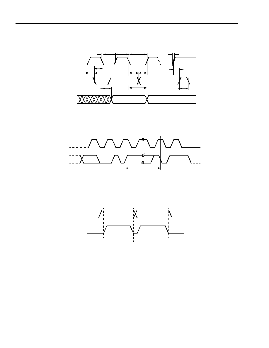
142
142
Agere Systems Inc.
FW323 05
Data Sheet, Rev. 2
1394A PCI PHY/Link Open Host Controller Interface
October 2001
ac Characteristics
(continued)
ROM_CLK: serial clock, ROM_AD: serial data I/O
1313 (F) R.02
Figure 5. Bus Timing
ROM_CLK: serial clock, ROM_AD: serial data I/O
1314 (F) R.02
Figure 6. Write Cycle Timing
ROM_CLK: serial clock, ROM_AD: serial data I/O
1310 (F) R.02
Figure 7. Data Validity
t
SETUP_START
t
HOLD_START
t
FALL_TIME
t
PW_LOW
t
PW_HIGH
t
RISE_TIME
t
SETUP_STOP
t
SETUP_DATA
t
HOLD_DATA
t
FREE
t
DATA_VALID
ROM_CLK
ROM_AD IN
ROM_AD OUT
t
HOLD_EEPROM
t
PW_LOW
ROM_CLK
ROM_AD
8TH BIT
ACK
WORD n
STOP
START
t
WR(1)
STABLE
STABLE
CHANGE
ROM_AD
ROM_CLK
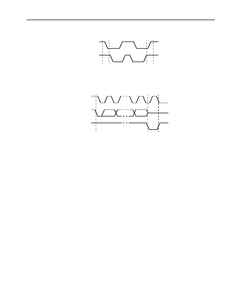
Agere Systems Inc.
143
Data Sheet, Rev. 2
FW323 05
October 2001
1394A PCI PHY/Link Open Host Controller Interface
ac Characteristics
(continued)
ROM_CLK: serial clock, ROM_AD: serial data I/O
1311 (F) R.02
Figure 8. Start and Stop Definition
ROM_CLK: serial clock
1312 (F) R.02
Figure 9. Output Acknowledge
START
STOP
ROM_AD
ROM_CLK
ROM_CLK
DATA IN
DATA OUT
START
ACK
1
8
9
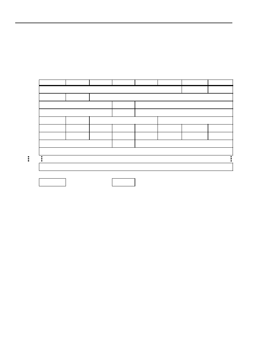
144
144
Agere Systems Inc.
FW323 05
Data Sheet, Rev. 2
1394A PCI PHY/Link Open Host Controller Interface
October 2001
Internal Register Configuration
PHY Core Register Map for Cable Environment
The PHY core register map is shown below in Table 128.
Table 128. PHY Core Register Map for the Cable Environment
Address
Contents
Bit 0
Bit 1
Bit 2
Bit 3
Bit 4
Bit 5
Bit 6
Bit 7
0000
2
Physical_ID
R
PS
0001
2
RHB
IBR
Gap_count
0010
2
Extended (7)
XXXXX
Total_ports
0011
2
Max_speed
XXXXX
Delay
0100
2
LCtrl
Contender
Jitter
Pwr_class
0101
2
Watchdog
ISBR
Loop
Pwr_fail
Timeout
Port_event Enab_accel Enab_multi
0110
2
XXXXX XXXXX XXXXX XXXXX XXXXX XXXXX XXXXX XXXXX
0111
2
Page_select
XXXXX
Port_select
1000
2
Register 0
Page_select
1111
2
Register 7
Page_select
REQUIRED
XXXXX
RESERVED

Agere Systems Inc.
145
Data Sheet, Rev. 2
FW323 05
October 2001
1394A PCI PHY/Link Open Host Controller Interface
Internal Register Configuration
(continued)
PHY Core Register Fields for Cable Environment
Table 129. PHY Core Register Fields for Cable Environment
Field
Size Type
Power Reset
Value
Description
Physical_ID
6
R
000000
The address of this node is determined during self-identification. A
value of 63 indicates a malconfigured bus; the link will not transmit
any packets.
R
1
R
0
When set to one, indicates that this node is the root.
PS
1
R
--
Cable power active.
RHB
1
RW
0
Root hold-off bit. When set to one, the force_root variable is TRUE,
which instructs the PHY core to attempt to become the root during
the next tree identify process.
IBR
1
RW
0
Initiate bus reset. When set to one, instructs the PHY core to set ibr
TRUE and reset_time to RESET_TIME. These values in turn cause
the PHY core to initiate a bus reset without arbitration; the reset
signal is asserted for 166
µ
s. This bit is self-clearing.
Gap_count
6
RW
3F
16
Used to configure the arbitration timer setting in order to optimize
gap times according to the topology of the bus. See Section 4.3.6
of
IEEE
Standard 1394-1995 for the encoding of this field.
Extended
3
R
7
This field has a constant value of seven, which indicates the
extended PHY core register map.
Total_ports
4
R
3
The number of ports implemented by this PHY core. This count
reflects the number.
Max_speed
3
R
010
2
Indicates the speed(s) this PHY core supports:
000
2
= 98.304 Mbits/s.
001
2
= 98.304 and 196.608 Mbits/s.
010
2
= 98.304, 196.608, and 393.216 Mbits/s.
011
2
= 98.304, 196.608, 393.216, and 786.43 Mbits/s.
100
2
= 98.304, 196.608, 393.216, 786.432, and
1,572.864 Mbits/s.
101
2
= 98.304, 196.608, 393.216, 786.432, 1,572.864, and
3,145.728 Mbits/s.
All other values are reserved for future definition.
Delay
4
R
0000
Worst-case repeater delay, expressed as 144 + (delay * 20) ns.
LCtrl
1
RW
1
Link Active. Cleared or set by software to control the value of the L
bit transmitted in the node's self-ID packet 0, which will be the logi-
cal AND of this bit and LPS active.
Contender
1
RW
See description Cleared or set by software to control the value of the C bit transmit-
ted in the self-ID packet. Powerup reset value is set by
CONTENDER pin.
Jitter
3
R
000
The difference between the fastest and slowest repeater data
delay, expressed as (jitter + 1) * 20 ns.
Pwr_class
3
RW
See description Power-Class. Controls the value of the pwr field transmitted in the
self-ID packet. See Section 4.3.4.1 of
IEEE
Standard 1394-1995 for
the encoding of this field. PC0, PC1, and PC2 pins set up power
reset value.

146
146
Agere Systems Inc.
FW323 05
Data Sheet, Rev. 2
1394A PCI PHY/Link Open Host Controller Interface
October 2001
Internal Register Configuration
(continued)
Table 129. PHY Core Register Fields for Cable Environment (continued)
Field
Size Type Power Reset Value
Description
Watchdog
1
RW
0
When set to one, the PHY core will set Port_event to one if
resume operations commence for any port.
ISBR
1
RW
0
Initiate Short (Arbitrated) Bus Reset. A write of one to this bit
instructs the PHY core to set ISBR true and reset_time to
SHORT_RESET_TIME. These values in turn cause the PHY
core to arbitrate and issue a short bus reset. This bit is self-
clearing.
Loop
1
RW
0
Loop Detect. A write of one to this bit clears it to zero.
Pwr_fail
1
RW
1
Cable Power Failure Detect. Set to one when the PS bit
changes from one to zero. A write of one to this bit clears it to
zero.
Timeout
1
RW
0
Arbitration State Machine Timeout. A write of one to this bit
clears it to zero (see MAX_ARB_STATE_TIME).
Port_event
1
RW
0
Port Event Detect. The PHY core sets this bit to one if any of
connected, bias, disabled, or fault change for a port whose
Int_enable bit is one. The PHY core also sets this bit to one if
resume operations commence for any port and Watchdog is
one. A write of one to this bit clears it to zero.
Enab_accel
1
RW
0
Enable Arbitration Acceleration. When set to one, the PHY
core will use the enhancements specified in clause 7.10 of
1394a-2000 specification. PHY core behavior is unspecified if
the value of Enab_accel is changed while a bus request is
pending.
Enab_multi
1
RW
0
Enable multispeed packet concatenation. When set to one, the
link will signal the speed of all packets to the PHY core.
Page_select
3
RW
000
Selects which of eight possible PHY core register pages are
accessible through the window at PHY core register addresses
1000
2
through 1111
2
, inclusive.
Port_select
4
RW
0000
If the page selected by Page_select presents per-port informa-
tion, this field selects which port's registers are accessible
through the window at PHY core register addresses 1000
2
through 1111
2
, inclusive. Ports are numbered monotonically
starting at zero, p0.

Agere Systems Inc.
147
Data Sheet, Rev. 2
FW323 05
October 2001
1394A PCI PHY/Link Open Host Controller Interface
Internal Register Configuration
(continued)
The port status page is used to access configuration and status information for each of the PHY core's ports. The
port is selected by writing zero to Page_select and the desired port number to Port_select in the PHY core register
at address 0111
2
. The format of the port status page is illustrated by Table 130 below; reserved fields are shown as
XXXXX. The meanings of the register fields with the port status page are defined by RSC.
Table 130. PHY Core Register Page 0: Port Status Page
Address
Contents
Bit 0
Bit 1
Bit 2
Bit 3
Bit 4
Bit 5
Bit 6
Bit 7
1000
2
AStat
BStat
Child
Connected
Bias
Disabled
1001
2
Negotiated_speed
Int_enable
Fault
XXXXX XXXXX XXXXX
1010
2
XXXXX XXXXX XXXXX XXXXX XXXXX XXXXX XXXXX XXXXX
1011
2
XXXXX XXXXX XXXXX XXXXX XXXXX XXXXX XXXXX XXXXX
1100
2
XXXXX XXXXX XXXXX XXXXX XXXXX XXXXX XXXXX XXXXX
1101
2
XXXXX XXXXX XXXXX XXXXX XXXXX XXXXX XXXXX XXXXX
1110
2
XXXXX XXXXX XXXXX XXXXX XXXXX XXXXX XXXXX XXXXX
1111
2
XXXXX XXXXX XXXXX XXXXX XXXXX XXXXX XXXXX XXXXX
REQUIRED
XXXXX
RESERVED

148
Agere Systems Inc.
FW323 05
Data Sheet, Rev. 2
1394A PCI PHY/Link Open Host Controller Interface
October 2001
Internal Register Configuration
(continued)
The meaning of the register fields with the port status page are defined by Table 131 below.
Table 131. PHY Core Register Port Status Page Fields
Field
Size Type
Power Reset
Value
Description
AStat
2
R
--
TPA line state for the port:
00
2
= invalid.
01
2
= 1.
10
2
= 0.
11
2
= Z.
BStat
2
R
--
TPB line state for the port (same encoding as AStat).
Child
1
R
0
If equal to one, the port is a child; otherwise, a parent. The
meaning of this bit is undefined from the time a bus reset is
detected until the PHY core transitions to state T1: child
handshake during the tree identify process (see Section
4.4.2.2 in
IEEE
Standard 1394-1995).
Connected
1
R
0
If equal to one, the port is connected.
Bias
1
R
0
If equal to one, incoming TPBIAS is detected.
Disabled
1
RW
0
If equal to one, the port is disabled.
Negotiated_speed
3
R
000
Indicates the maximum speed negotiated between this PHY
core port and its immediately connected port; the encoding is
the same as for they PHY core register Max_speed field.
Int_enable
1
RW
0
Enable port event interrupts. When set to one, the PHY core
will set Port_event to one if any of connected, bias, disabled,
or fault (for this port) change state.
Fault
1
RW
0
Set to one if an error is detected during a suspend or resume
operation. A write of one to this bit clears it to zero.
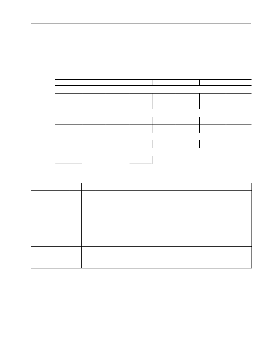
Agere Systems Inc.
149
Data Sheet, Rev. 2
FW323 05
October 2001
1394A PCI PHY/Link Open Host Controller Interface
Internal Register Configuration
(continued)
The vendor identification page is used to identify the PHY core's vendor and compliance level. The page is
selected by writing one to Page_select in the PHY core register at address 0111
2
. The format of the vendor identi-
fication page is shown in Table 132; reserved fields are shown as XXXXX.
Table 132. PHY Core Register Page 1: Vendor Identification Page
Note: The meaning of the register fields within the vendor identification page are defined by Table 133.
Table 133. PHY Core Register Vendor Identification Page Fields
Note: The vendor-dependent page provides access to information used in the manufacturing test of the FW323.
Address
Contents
Bit 0
Bit 1
Bit 2
Bit 3
Bit 4
Bit 5
Bit 6
Bit 7
1000
2
Compliance_level
1001
2
XXXXX XXXXX XXXXX XXXXX XXXXX XXXXX XXXXX XXXXX
1010
2
1011
2
Vendor_ID
1100
2
1101
2
1110
2
Product_ID
1111
2
REQUIRED
XXXXX
RESERVED
Field
Size Type
Description
Compliance_level
8
r
Standard to which the PHY core implementation complies:
0 = not specified
1 =
IEEE
1394a-2000
Agere's FW323 compliance level is 1.
All other values reserved for future standardization.
Vendor_ID
24
r
The company ID or organizationally unique identifier (OUI) of the manufacturer
of the PHY core. Agere's vendor ID is 00601D
16
. This number is obtained from
the
IEEE
registration authority committee (RAC). The most significant byte of
Vendor_ID appears at PHY core register location 1010
2
and the least significant
at 1100
2
.
Product_ID
24
r
The meaning of this number is determined by the company or organization that
has been granted Vendor_ID. Agere's FW323 PHY core product ID is 032304
16
.
The most significant byte of Product_ID appears at PHY core register location
1101
2
and the least significant at 1111
2
.
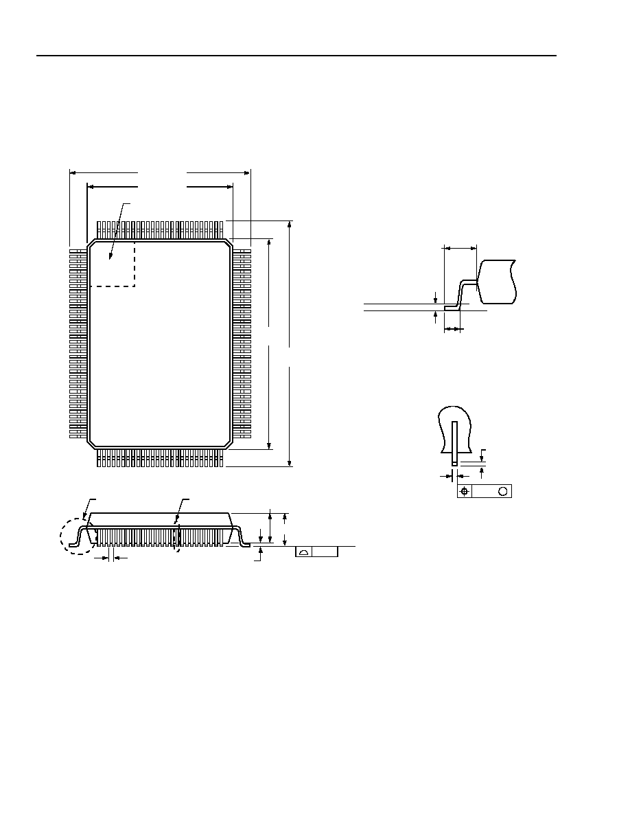
150
Agere Systems Inc.
FW323 05
Data Sheet, Rev. 2
1394A PCI PHY/Link Open Host Controller Interface
October 2001
Outline Diagrams
128-Pin TQFP
Dimensions are in millimeters.
5-4427r.2 (F)
0.19/0.27
0.08
M
0.106/0.200
DETAIL B
0.25
0.45/0.75
1.00 REF
GAGE PLANE
SEATING PLANE
DETAIL A
DETAIL A
DETAIL B
1.60 MAX
0.50 TYP
SEATING PLANE
0.08
1.40
±
0.05
0.05/0.15
1
38
65
102
103
128
PIN #1 IDENTIFIER ZONE
16.00
±
0.20
14.00
±
0.20
20.00
±
0.20
22.00
±
0.20
64
39

Agere Systems Inc.
151
Data Sheet, Rev. 2
FW323 05
October 2001
1394A PCI PHY/Link Open Host Controller Interface
Notes

Agere Systems Inc. reserves the right to make changes to the product(s) or information contained herein without notice. No liability is assumed as a result of their use or application.
Copyright © 2001 Agere Systems Inc.
All Rights Reserved
October 2001
DS01-124CMPR-2 (Replaces DS01-124CMPR-1)
For additional information, contact your Agere Systems Account Manager or the following:
INTERNET:
http://www.agere.com
E-MAIL:
docmaster@agere.com
N. AMERICA:
Agere Systems Inc., 555 Union Boulevard, Room 30L-15P-BA, Allentown, PA 18109-3286
1-800-372-2447, FAX 610-712-4106 (In CANADA: 1-800-553-2448, FAX 610-712-4106)
ASIA:
Agere Systems Hong Kong Ltd., Suites 3201 & 3210-12, 32/F, Tower 2, The Gateway, Harbour City, Kowloon
Tel. (852) 3129-2000, FAX (852) 3129-2020
CHINA: (86) 21-5047-1212 (Shanghai), (86) 10-6522-5566 (Beijing), (86) 755-695-7224 (Shenzhen)
JAPAN: (81) 3-5421-1600 (Tokyo), KOREA: (82) 2-767-1850 (Seoul), SINGAPORE: (65) 778-8833, TAIWAN: (886) 2-2725-5858 (Taipei)
EUROPE:
Tel. (44) 7000 624624, FAX (44) 1344 488 045
FW323 05
Data Sheet, Rev. 2
1394A PCI PHY/Link Open Host Controller Interface
October 2001
Microsoft
and
Windows
are registered trademarks of Microsoft Corporation.
MacOS
is a registered trademark of Apple Computer, Inc.
IEEE
is a registered trademark of The Institute of Electrical and Electronics Engineers, Inc.