 | –≠–ª–µ–∫—Ç—Ä–æ–Ω–Ω—ã–π –∫–æ–º–ø–æ–Ω–µ–Ω—Ç: FW801BF | –°–∫–∞—á–∞—Ç—å:  PDF PDF  ZIP ZIP |

Data Sheet
January 2005
FW801BF Low-Power PHY 1394a-2000
One-Cable Transceiver/Arbiter Device
TM
TM
Distinguishing Features
Compliant with IEEE
Æ
Standard 1394a-2000,
IEEE Standard for a High Performance Serial
Bus Amendment 1.
Low power consumption during powerdown or
microlow-power sleep mode.
Supports extended BIAS_HANDSHAKE time for
enhanced interoperability with camcorders.
While unpowered and connected to the bus, will
not drive TPBIAS on a connected port even if
receiving incoming bias voltage on that port.
Does not require external filter capacitors for PLL.
Does not require a separate 5 V supply for 5 V link
controller interoperability.
Interoperable across 1394 cable with 1394 physi-
cal layers (PHY) using 5 V supplies.
Interoperable with 1394 link-layer controllers using
5 V supplies.
1394a-2000 compliant common mode noise filter
on incoming TPBIAS.
Powerdown features to conserve energy in bat-
tery-powered applications include the following:
-- Device powerdown ball.
-- Link interface disable using LPS.
-- Inactive ports power down.
-- Automatic microlow-power sleep mode during
suspend.
Interface to link-layer controller supports Annex J
electrical isolation as well as bus-keeper isolation.
Features
Provides one fully compliant cable port at
100 Mbits/s, 200 Mbits/s, and 400 Mbits/s.
Fully supports 1394 Open HCI requirements.
Supports arbitrated short bus reset to improve
utilization of the bus.
Supports ack-accelerated arbitration and fly-by con-
catenation.
Supports connection debounce.
Supports multispeed packet concatenation.
Supports PHY pinging and remote PHY access
packets.
Fully supports suspend/resume.
Supports PHY-link interface initialization and reset.
Supports 1394a-2000 register set.
Supports LPS/link-on as a part of PHY-link inter-
face.
Supports provisions of IEEE 1394-1995 Standard
for a High Performance Serial Bus.
Fully interoperable with FireWire
Æ
and i.LINK
Æ
implementations of IEEE 1394-1995.
Reports cable power fail interrupt when voltage at
CPS ball falls below 7.5 V.
Provides separate cable bias and driver termination
voltage supply for port.
Other Features
48-ball VTFSBGAC package.
Single 3.3 V supply operation.
Data interface to link-layer controller provided
through 2/4/8 parallel lines at 50 Mbits/s.
25 MHz crystal oscillator and PLL provide a
50 MHz link-layer controller clock as well as trans-
mit/receive data at 100 Mbits/s, 200 Mbits/s, and
400 Mbits/s.
Multiple separate package signals provided for
analog and digital supplies and grounds.
Description
The Agere Systems FW801BF device provides the
analog physical layer functions needed to imple-
ment a one-port node in a cable-based IEEE 1394-
1995 and IEEE 1394a-2000 network.
The cable port incorporates two differential line trans-
ceivers. The transceivers include circuitry to monitor
the line conditions as needed for determining con-
nection status, for initialization and arbitration, and
for packet reception and transmission. The PHY is
designed to interface with a link-layer controller
(LLC).

2
Agere Systems Inc.
Data Sheet
January 2005
One-Cable Transceiver/Arbiter Device
FW801BF PHY 1394a-2000
Table of Contents
Contents
Page
Distinguishing Features ............................................................................................................................................1
Features ...................................................................................................................................................................1
Other Features ......................................................................................................................................................... 1
Description ................................................................................................................................................................1
Ball Information ........................................................................................................................................................ 6
Signal Information..................................................................................................................................................... 7
Application Information ...........................................................................................................................................10
Crystal Selection Considerations ............................................................................................................................11
Load Capacitance ............................................................................................................................................ 12
Adjustment to Crystal Loading .........................................................................................................................12
Crystal/Board Layout .......................................................................................................................................12
1394 Application Support Contact Information .......................................................................................................12
Absolute Maximum Ratings ....................................................................................................................................13
Electrical Characteristics ........................................................................................................................................14
Timing Characteristics ............................................................................................................................................17
Timing Waveforms ..................................................................................................................................................18
Internal Register Configuration ...............................................................................................................................19
Outline Diagrams ....................................................................................................................................................24
48-Ball TFSBGAC ............................................................................................................................................24
Ordering Information ...............................................................................................................................................25
List of Figures
Figures
Page
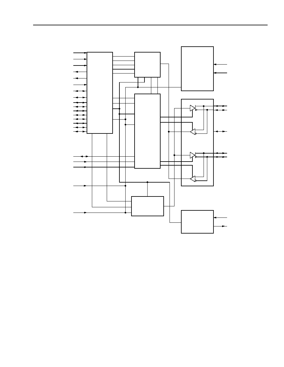
Figure 1. Block Diagram.............................................................................................................................................. 5
Figure 2. FW801BF Ball Diagram (48-Ball TFSBGAC) Top View ...............................................................................6
Figure 3. Typical External Component Connections .................................................................................................10
Figure 4. Typical Port Termination Network .............................................................................................................11
Figure 5. Crystal Circuitry .........................................................................................................................................12
Figure 6. Dn, CTLn, and LREQ Input Setup and Hold Times Waveforms ................................................................18
Figure 7. Dn, CTLn Output Delay Relative to SYSCLK Waveforms .........................................................................18
List of Tables
Tables
Page
Table 1. FW801BF (48-Ball TFSBGAC) Ball Coordination Table ............................................................................ 6
Table 2. Signal Descriptions .....................................................................................................................................7
Table 3. Absolute Maximum Ratings ......................................................................................................................13
Table 4. Analog Characteristics ..............................................................................................................................14
Table 5. Driver Characteristics ...............................................................................................................................15
Table 6. Device Characteristics ..............................................................................................................................16
Table 7. Switching Characteristics ......................................................................................................................... 17
Table 8. Clock Characteristics................................................................................................................................ 17
Table 9. PHY Register Map for the Cable Environment ........................................................................................ 19
Table 10. PHY Register Fields for the Cable Environment .....................................................................................19
Table 11. PHY Register Page 0: Port Status Page ................................................................................................ 21
Table 12. PHY Register Port Status Page Fields ................................................................................................... 22
Table 13. PHY Register Page 1: Vendor Identification Page ............................................................................... 23
Table 14. PHY Register Vendor Identification Page Fields .................................................................................... 23

Data Sheet
FW801BF PHY 1394a-2000
January 2005
One-Cable Transceiver/Arbiter Device
Agere Systems Inc.
3
Description
(continued)
The PHY requires either an external 24.576 MHz crys-
tal or crystal oscillator. The internal oscillator drives an
internal phase-locked loop (PLL) that generates the
required 393.216 MHz reference signal. The 393.216
MHz reference signal is internally divided to provide
the 49.152 MHz, 98.304 MHz, and 196.608 MHz clock
signals that control transmission of the outbound
encoded strobe and data information. The 49.152 MHz
clock signal is also supplied to the associated LLC for
synchronization of the two chips and is used for resyn-
chronization of the received data. The powerdown
function, when enabled by the PD signal high, stops
operation of the PLL and disables all circuitry except
the cable-not-active (CNA) signal circuitry.
The PHY supports an isolation barrier between itself
and its LLC. When ISON is tied high, the link interface
outputs behave normally. When ISON is tied low, inter-
nal differentiating logic is enabled, and the outputs
become short pulses that can be coupled through a
capacitor or transformer as described in the
IEEE 1394-1995 Annex J. To operate with bus-keeper
isolation, the ISON ball of the FW801BF must be tied
high.
Data bits to be transmitted through the cable port is
received from the LLC on two, four, or eight data lines
(D[0:7]), and are latched internally in the PHY in syn-
chronization with the 49.152 MHz system clock. These
bits are combined serially, encoded, and transmitted at
98.304 Mbits/s, 196.608 Mbits/s, or 393.216 Mbits/s as
the outbound data-strobe information stream. During
transmission, the encoded data information is transmit-
ted differentially on the TPA and TPB cable pair(s).
During packet reception, the TPA and TPB transmit-
ters of the receiving cable port are disabled and the
receivers for that port are enabled. The encoded data
information is received on the TPA and TPB cable
pair. The received data-strobe information is decoded
to recover the receive clock signal and the serial data
bits. The serial data bits are split into two (for S100),
four (for S200), or eight (for S400) parallel streams,
resynchronized to the local system clock, and sent to
the associated LLC. The received data is also trans-
mitted (repeated) out of the other active (connected)
cable ports.
Both the TPA and TPB cable interfaces incorporate
differential comparators to monitor the line states dur-
ing initialization and arbitration. The outputs of these
comparators are used by the internal logic to deter-
mine the arbitration status. The TPA channel monitors
the incoming cable common-mode voltage. The value
of this common-mode voltage is used during arbitra-
tion to set the speed of the next packet transmission.
In addition, the TPB channel monitors the incoming
cable common-mode voltage for the presence of the
remotely supplied twisted-pair bias voltage. This moni-
tor is called bias-detect.
The TPBIAS circuit monitors the value of incoming
TPA pair common-mode voltage when local TPBIAS is
inactive. Because this circuit has an internal current
source and the connected node has a current sink, the
monitored value indicates the cable connection status.
This monitor is called connect-detect.
Both the TPB bias-detect monitor and TPBIAS con-
nect-detect monitor are used in suspend/resume
signaling and cable connection detection.
The PHY provides a 1.86 V nominal bias voltage for
driver load termination. When seen through a cable by
a remote receiver, this bias voltage indicates the pres-
ence of an active connection. The value of this bias
voltage has been chosen to allow interoperability
between transceiver chips operating from 5 V or 3 V
nominal supplies. This bias voltage source should be
stabilized by using an external filter capacitor of
approximately 0.33
µ
F.
The transmitter circuitry, the receiver circuitry, and the
twisted-pair bias voltage circuity are all disabled with a
powerdown condition. The powerdown condition
occurs when the PD input is high. The port transmitter
circuitry, the receiver circuitry, and the TPBIAS output
are also disabled when the port is disabled, sus-
pended, or disconnected.
The line drivers in the PHY operate in a high-imped-
ance current mode and are designed to work with
external 112
line-termination resistor networks. One
network is provided at each end of each twisted-pair
cable. Each network is composed of a pair of series-
connected 56
resistors. The midpoint of the pair of
resistors that is directly connected to the twisted-pair A
(TPA) signals is connected to the TPBIAS voltage sig-
nal. The midpoint of the pair of resistors that is directly
connected to the twisted-pair B (TPB) signals is cou-
pled to ground through a parallel RC network with
recommended resistor and capacitor values of 5 k
and 220 pF, respectively. The value of the external
resistors are specified to meet the
IEEE 1394
standard
specifications when connected in parallel with the
internal receiver circuits.
The driver output current, along with other internal
operating currents, is set by an external resistor. This
resistor is connected between the R0 and R1 signals
and has a value of 2.49 k
±
1%.

FW801BF PHY 1394a-2000
Data Sheet
One-Cable Transceiver/Arbiter Device
January 2005
4
Agere Systems Inc.
Description
(continued)
The FW801BF supports suspend/resume as defined in
the IEEE 1394a-2000 specification. The suspend
mechanism allows the FW801BF port to be put into a
suspended state. In this state, the port is unable to
transmit or receive data packets; however, it remains
capable of detecting connection status changes and
detecting incoming TPBias. When the FW801BF port
is suspended, all circuits except the bias voltage refer-
ence generator and the bias detection circuits are
powered down, resulting in significant power savings.
The use of suspend/resume is recommended.
As an input, the C_LKON signal indicates whether a
node is a contender for bus manager. When the
C_LKON signal is asserted, it means the node is a
contender for bus manager. When the signal is not
asserted, it means that the node is not a contender.
The C bit corresponds to bit 20 in the self-ID packet
(see Section 4.3.4.1 of the IEEE 1394a-2000 standard
for additional details).
The power class (Pwr_class) bits of the self-ID packet
have a default value of 4, i.e., power class 100. These
bits can be read and modified through the LLC using
Figure 5B-1 (PHY Register Map) of the IEEE 1394a-
2000 standard. See Table 9 of this document for the
address space of the Pwr_class register.
A powerdown signal (PD) is provided to allow a power-
down mode where most of the PHY circuits are
powered down to conserve energy in battery-powered
applications. The internal logic in FW801BF is reset as
long as the powerdown signal is asserted. A cable sta-
tus signal (CNA) provides a high output when the
twisted-pair cable port is receiving incoming bias volt-
age. This output is not debounced. The CNA output
can be used to determine when to power the PHY
down or up. In the powerdown mode, all circuitry is
disabled except the CNA circuitry. It should be noted
that when the device is powered down, it does not act
in a repeater mode.
When the power supply of the PHY is removed while
the twisted-pair cables are connected, the PHY trans-
mitter and receiver circuitry is designed to present a
high impedance to the cable in order to not load the
TPBIAS signal voltage on the other end of the cable.
Whenever the TBA±/TPB± signals are wired to a con-
nector, they must be terminated using the normal
termination network (See Figure 4.). This is required
for reliable operation. When the port does not have a
cable connected, internal connect-detect circuitry will
keep the port in a disconnected state.
All gap counts on all nodes of a 1394 bus must be
identical. The software accomplishes this by issuing
PHY configuration packets (see Section 4.3.4.3 of the
IEEE 1394a-2000 standard) or by issuing two bus
resets, which resets the gap counts to the maximum
level (3Fh).
The link power status (LPS) signal works with the
C_LKON signal to manage the LLC power usage of
the node. The LPS signal indicates that the LLC of the
node is powered up or powered down. If LPS is inac-
tive for more than 1.2
µ
s and less than 25
µ
s, the
PHY/link interface is reset. If LPS is inactive for greater
than 25
µ
s, the PHY will disable the PHY/link interface
to save power. FW801BF continues its repeater func-
tion even when the PHY/link interface is disabled. If
the PHY then receives a link-on packet, the C_LKON
signal is activated to output a 6.114 MHz signal that
can be used by the LLC to power itself up. Once the
LLC is powered up, the LPS signal communicates this
to the PHY and the PHY/link interface is enabled.
C_LKON signal is turned off when LPS is active or
when a bus reset occurs, provided the interrupt that
caused C_LKON is not present.
When the PHY/link interface is in the disabled state,
the FW801BF will automatically enter a low-power
mode if all ports are inactive (disconnected, disabled,
or suspended). In this low-power mode, the FW801BF
disables its PLL and also disables parts of its refer-
ence circuitry depending on the state of the port (some
reference circuitry must remain active in order to
detect incoming TP bias). The lowest power consump-
tion (the microlow-power sleep mode) is attained when
the port is either disconnected or disabled with the port
interrupt enable bit (See Table 12) cleared. The
FW801BF will exit the low-power mode when the LPS
input is asserted high or when a port event occurs that
requires the FW801BF to become active in order to
respond to the event or to notify the LLC of the event
(e.g., incoming bias or disconnection is detected on a
suspended port, a new connection is detected on a
nondisabled port, etc.). When the FW801BF is in the
low-power mode, the SYSCLK output will become
active (and the PHY/link interface will be initialized and
become operative) within 3 ms after LPS is asserted
high.
Two of the FW801BF's signals are used to set up vari-
ous test conditions used only during the device
manufacturing process. These signals (SE and SM)
should be connected to V
SS
for normal operation.
Agere Systems Inc.
5
Data Sheet
January 2005
One-Cable Transceiver/Arbiter Device
FW801BF PHY 1394a-2000
Description
(continued)
5-5459.e (F)
Figure 1. Block Diagram
LINK
INTERFACE
I/O
RECEIVED
DATA
DECODER/
ARBITRATION
AND
CONTROL
RETIMER
STATE
MACHINE
LOGIC
BIAS
VOLTAGE
AND
CURRENT
GENERATOR
OSCILLATOR,
PLL SYSTEM,
AND
CLOCK
GENERATOR
TRANSMIT
DATA
ENCODER
CABLE PORT 0
TPA[0]
TPAN[0]
TPB[0]
TPBN[0]
R[0]
R[1]
XI
XO
CPS
LPS
ISON
CNA
SYSCLK
LREQ
CTL[0]
CTL[1]
D[0]
D[1]
D[2]
D[3]
C_LKON
SE
SM
PD
RESETN
CRYSTAL
D[4]
D[5]
D[6]
D[7]
TPBIAS[0]
6
Agere Systems Inc.
Data Sheet
January 2005
One-Cable Transceiver/Arbiter Device
FW801BF PHY 1394a-2000
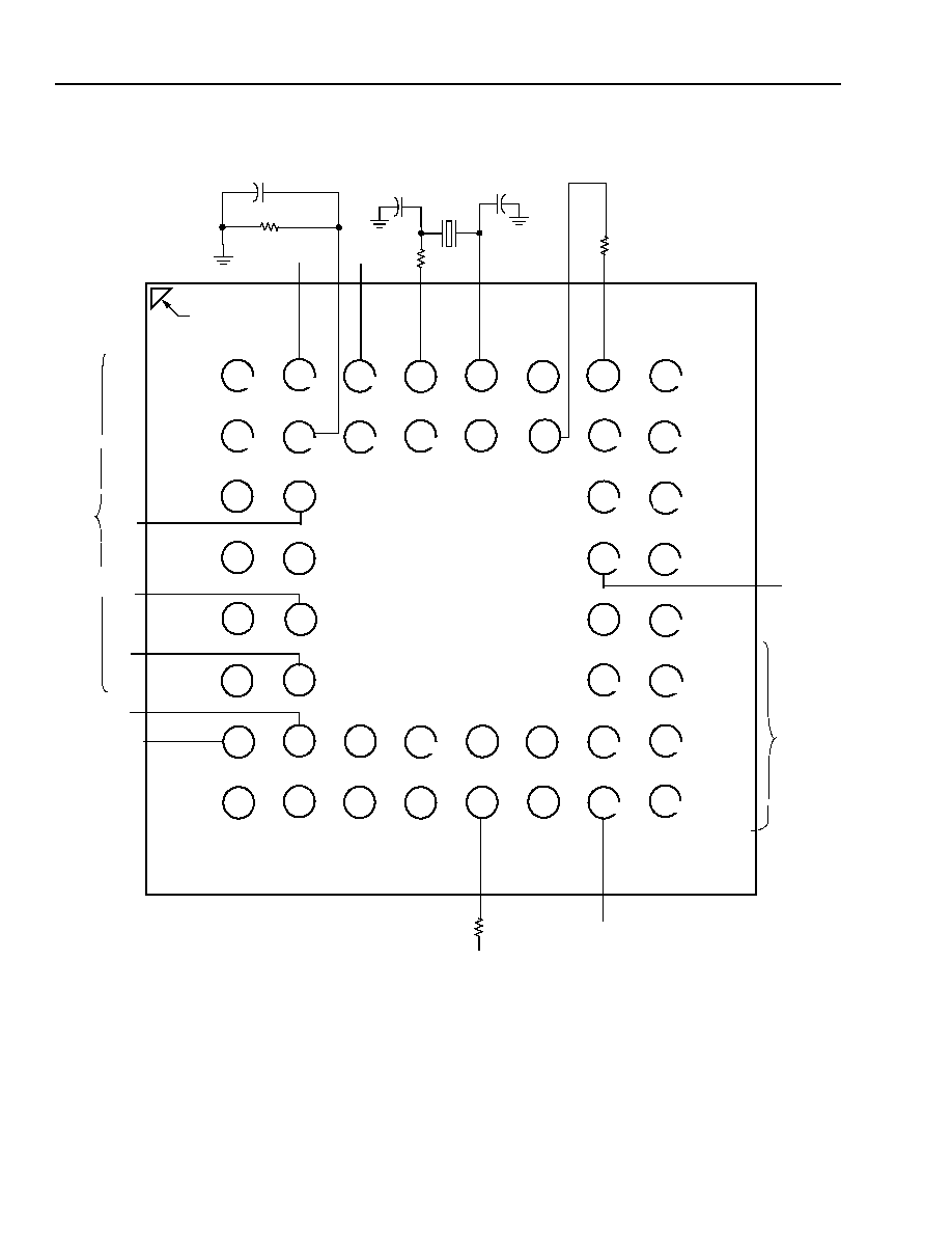
Ball Information
Note: Refer to the outline drawing on page 24 for a bottom view.
5-8117
Figure 2. FW801BF Ball Diagram (48-Ball TFSBGAC) Top View
Table 1. FW801BF (48-Ball TFSBGAC) Ball Coordination Table
Ball
Number
Ball Name
Ball
Number
Ball Name
Ball
Number
Ball Name
Ball
Number
Ball Name
A1
CTL[0]
B5
V
DD
E1
D[5]
G5
V
SS
A2
LREQ
B6
R[1]
E2
D[3]
G6
V
SS
A3
SYSCLK
B7
V
SSA
E7
SE
G7
V
DDA
A4
XO
B8
Not Used
E8
Not Used
G8
TPAN[0]
A5
XI
C1
D[1]
F1
D[7]
H1
CNA
A6
V
SS
C2
D[0]
F2
D[4]
H2
V
DD
A7
R[0]
C7
V
DDA
F7
V
SSA
H3
PD
A8
Not Used
C8
Not Used
F8
TPA[0]
H4
ISON
B1
CTL[1]
D1
D[2]
G1
LPS
H5
CPS
B2
RESETN
D2
V
DD
G2
D[6]
H6
SM
B3
V
SS
PLL
D7
TPBIAS[0]
G3
V
SS
H7
TPB[0]
B4
V
DD
PLL
D8
Not Used
G4
C_LKON
H8
TPBN[0]
A
B
C
D
E
F
G
H
A
B
C
D
E
F
G
H
1 2 3 4 5 6 7 8
A1 BALL PAD CORNER
1 2 3 4 5 6 7 8

Agere Systems Inc.
7
Data Sheet
January 2005
One-Cable Transceiver/Arbiter Device
FW801BF PHY 1394a-2000
Signal Information
Table 2. Signal Descriptions
Ball
Number
Signal*
Type
Name/Description
G4
C_LKON
I/O
Bus Manager Capable Input and Link-On Output. On hardware reset
(RESETN), this ball is used to set the default value of the contender status
indicated during self-ID. The bit value programming is done by tying the
signal through a 10 k
resistor to V
DD
(high, bus manager capable) or to
GND (low, not bus manager capable). Using either the pull-up or pull-
down resistor allows the link-on output to override the input value when
necessary.
After hardware reset, this ball is set as an output. If the LPS is inactive,
C_LKON indicates one of the following events by asserting a 6.114 MHz
signal.
1. FW801BF receives a link-on packet addressed to this node.
2. Port_event register bit is 1.
3. Any of the Timeout, Pwr_fail, or Loop register bits are 1 and the
Watchdog register bit is also 1.
4. Once activated, the C_LKON output will continue active until the LPS
becomes active. The PHY also deasserts the C_LKON output when a
1394 bus reset occurs, if the C_LKON is active due solely to the recep-
tion of a link-on packet.
Note: If an interrupt condition exists that would otherwise cause the
C_LKON output to be activated if the LPS were inactive, the
C_LKON output will be activated when the LPS subsequently
becomes inactive.
H1
CNA
O
Cable-Not-Active Output. CNA is asserted high when none of the PHY
ports are receiving an incoming bias voltage. This circuit remains active
during the powerdown mode.
H5
CPS
I
Cable Power Status. CPS is normally connected to the cable power
through a 400 k
resistor. This circuit drives an internal comparator that
detects the presence of cable power. This information is maintained in one
internal register and is available to the LLC by way of a register read (see
Table 9, address register 0000
2
, bit 7/PS). In applications that do not sink
or source 1394 power (VP), this ball can be tied to ground.
Note: When this ball is grounded, the Pwr_fail bit in PHY register 0101
2
will
be set.
A1
CTL[0]
I/O
Control I/O. The CTLn signals are bidirectional communications control
signals between the PHY and the LLC. These signals control the passage
of information between the two devices. Bus-keeper circuitry is built into
these terminals.
B1
CTL[1]
C1, C2, D1,
E1, E2, F1,
F2, G2
D[0:7]
I/O
Data I/O. The Dn signals are bidirectional and pass data between the PHY
and the LLC. Bus-keeper circuitry is built into these terminals.
* Active-low signals are indicated by "N" at the end of signal names, within this document.

8
Agere Systems Inc.
Data Sheet
January 2005
One-Cable Transceiver/Arbiter Device
FW801BF PHY 1394a-2000
Signal Information
(continued)
Table 2. Signal Descriptions (continued)
Ball
Number
Signal*
Type
Name/Description
H4
ISON
I
Link Interface Isolation Disable Input (Active-Low). ISON controls the
operation of an internal pulse differentiating function used on the
PHY-LLC interface signals, CTLn and Dn, when they operate as outputs.
When ISON is asserted low, the isolation barrier is implemented between
PHY and its LLC (as described in Annex J of IEEE 1394-1995).
ISON is normally tied high to disable isolation differentiation. Bus-keepers
are enabled when ISON is high (inactive) on CTLn, Dn, and LREQ. When
ISON is low (active), the bus-keepers are disabled. Please refer to
Agere's application note, 1394 Isolation (AP05-014CMPR) for more infor-
mation.
G1
LPS
I
Link Power Status. LPS is connected to either the V
DD
supplying the
LLC or to a pulsed output that is active when the LLC is powered for the
purpose of monitoring the LLC power status. If LPS is inactive for more
than 1.2
µ
s and less than 25
µ
s, the PHY-link interface is reset. If LPS is
inactive for greater than 25
µ
s, the PHY will disable the PHY/link interface
to save power. FW801BF continues its repeater function.
A2
LREQ
I
Link Request. LREQ is an output from the LLC that requests the PHY to
perform some service. Bus-keeper circuitry is built into this terminal.
H3
PD
I
Powerdown. When asserted high, PD turns off all internal circuitry except
the bias-detect circuits that drive the CNA signal. Internal FW801BF logic
is kept in the reset state as long as PD is asserted. The PD terminal is
provided for backward compatibility. It is recommended that the FW801BF
be allowed to manage its own power consumption using suspend/resume
in conjunction with LPS. C_LKON features are defined in the IEEE 1394a-
2000 specification.
B4
V
DD
PLL
--
Power for PLL Circuit. V
DD
PLL supplies power to the PLL circuitry
portion of the device.
B3
V
SS
PLL
--
Ground for PLL Circuit. V
SS
PLL is tied to a low-impedance ground
plane.
A7
R[0]
I
Current Setting Resistor. An internal reference voltage is applied to a
resistor connected between R0 and R1 to set the operating current and
the cable driver output current. A low temperature-coefficient resistor
(TCR) with a value of 2.49 k
±
1% should be used to meet the IEEE
1394-1995 standard requirements for output voltage limits.
B6
R[1]
B2
RESETN
I
Reset (Active-Low). When RESETN is asserted low (active), a 1394 bus
reset condition is set on the active cable port and the FW801BF is reset to
the reset start state. To guarantee that the PHY will reset, this ball must be
held low for at least 2 ms. An internal pull-up resistor connected to V
DD
is
provided so that only an external delay capacitor (0.1
µ
F) and resistor
(510 k
) in parallel, are required to connect this ball to ground. This
circuitry will ensure that the capacitor will be discharged when PHY power
is removed. The input is a standard logic buffer and can also be driven by
an open-drain logic output buffer. Do not leave this ball unconnected.
E7
SE
I
Test Mode Control. SE is used during Agere's manufacturing test and
should be tied to V
SS
for normal operation.
* Active-low signals are indicated by "N" at the end of signal names, within this document.

Agere Systems Inc.
9
Data Sheet
January 2005
One-Cable Transceiver/Arbiter Device
FW801BF PHY 1394a-2000
H6
SM
I
Test Mode Control. SM is used during Agere's manufacturing test and
should be tied to V
SS
for normal operation.
A3
SYSCLK
O
System Clock. SYSCLK provides a 49.152 MHz clock signal, which is
synchronized with the data transfers to the LLC.
F8
TPA[0]
Analog I/O Port0, Port Cable Pair A. TPA0± is the port A connection to the twisted-
pair cable. Board traces from each pair of positive and negative differen-
tial signal balls should be kept as short as possible and matched to the
external load resistors and to the cable connector.
G8
TPAN[0]
H7
TPB[0]
Analog I/O Port0, Port Cable Pair B. TPB0± is the port B connection to the twisted-
pair cable. Board traces from each pair of positive and negative differen-
tial signal balls should be kept as short as possible and matched to the
external load resistors and to the cable connector.
H8
TPBN[0]
D7
TPBIAS[0]
Analog I/O Port0, Twisted-Pair Bias. TPBIAS provides the 1.86 V nominal bias
voltage needed for proper operation of the twisted-pair cable drivers and
receivers and for sending a valid cable connection signal to the remote
nodes.
B5, D2,
H2
V
DD
--
Digital Power. V
DD
supplies power to the digital portion of the device.
C7, G7
V
DDA
--
Analog Circuit Power. V
DDA
supplies power to the analog portion of the
device.
A6, G3,
G5, G6
V
SS
--
Digital Ground. All V
SS
signals should be tied to the low-impedance
ground plane.
B7, F7
V
SSA
--
Analog Circuit Ground. All V
SSA
signals should be tied together to a low-
impedance ground plane.
A5
XI
--
Crystal Oscillator. XI and XO connect to a 24.576 MHz parallel resonant
fundamental mode crystal. Although, when a 24.576 MHz clock source is
used, it can be connected to XI with XO left unconnected. The optimum
values for the external load capacitors and resistor are dependent on the
specifications of the crystal used. It is necessary to add an external series
resistor (RL) to the XO ball (see Figures 3 and 5). For more details, refer
to the Crystal Selection Considerations section in this data sheet. Note
that it is very important to place the crystal as close as possible to the XO
and XI balls, i.e., within 0.5 in./1.27 cm.
A4
XO
Signal Information
(continued)
Table 2. Signal Descriptions (continued)
Ball
Number
Signal*
Type
Name/Description
* Active-low signals are indicated by "N" at the end of signal names, within this document.
10
Agere Systems Inc.
Data Sheet
January 2005
One-Cable Transceiver/Arbiter Device
FW801BF PHY 1394a-2000
Application Information
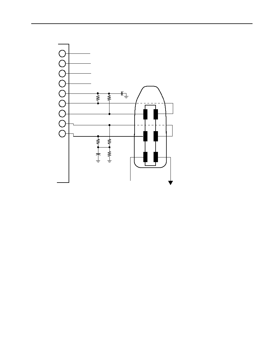
5-6767.a (F)
* See Figure 4 for typical port termination network.
Figure 3. Typical External Component Connections
NOT USED
NOT USED
NOT USED
NOT USED
NOT USED
TPA[0]
TPAN[0]
TPBN[0]
R[0]
VSSA
TPBIAS[0]
SE
VSSA
VDDA
TPB[0]
SM
VSS
R[1]
VSS
XI
XO
SYSCLK
LREQ
CTL[0]
CTL[1]
D[1]
D[2]
D[5]
D[7]
LPS
CNA
RESETN
VSSPLL
VDDPLL
VDD
D[0]
VDD
D[3]
D[4]
D[6]
VSS
C_LKON
VSS
VDD
PD
ISON
CPS
VDDA
2.49 k
PORT 0*
400 k
CA
BLE
POWER
0.1
µ
F
A1 BALL
AGERE FW801BF
LCC PULSE
OR V
DD
LL
C
PORT
0*
PAD CORNER
PORT 0*
LLC
LLC
LLC
LLC
LLC
LL
C
510 k
24.576 MHz
CL
CL
RL
Agere Systems Inc.
11
Data Sheet
January 2005
One-Cable Transceiver/Arbiter Device
FW801BF PHY 1394a-2000
Application Information
(continued)
5-7654 (F)
Figure 4. Typical Port Termination Network
Crystal Selection Considerations
The FW801BF is designed to use an external 24.576 MHz parallel resonant fundamental mode crystal connected
between the XI and XO terminals to provide the reference for an internal oscillator circuit. The IEEE 1394a-2000
standard requires that FW801BF have less than ±100 ppm total variation from the nominal data rate, which is
directly influenced by the crystal. To achieve this, it is recommended that an oscillator with a nominal 50 ppm or
less frequency tolerance be used.
The total frequency variation must be kept below
±
100 ppm from nominal with some allowance for error introduced
by board and device variations. Trade-offs between frequency tolerance and stability may be made as long as the
total frequency variation is less than
±
100 ppm.
TPBIAS[0]
TPA[0]
TPAN[0]
TPB[0]
TPBN[0]
56
56
56
56
5 k
220 pF
0.33
µ
F
1
3
5
2
4
6
IEEE 1394-1995 STANDARD
CONNECTOR
VG
VP
CABLE
POWER
V
DDA
V
DDA
V
SSA
V
SSA
B7
F7
C7
G7
D7
F8
G8
H7
H8
G8
12
Agere Systems Inc.
Data Sheet
January 2005
One-Cable Transceiver/Arbiter Device
FW801BF PHY 1394a-2000
Crystal Selection Considerations
(continued)
Load Capacitance
The frequency of oscillation is dependent upon the load capacitance specified for the crystal, in parallel resonant
mode crystal circuits. Total load capacitance (C
L
) is a function of not only the discrete load capacitors, but also
capacitances from the FW801BF board traces and capacitances of the other FW801BF connected components.
The values for load capacitors (C
A
and C
B
) should be calculated using this formula:
C
A
= C
B
= (C
L
≠ C
stray
)
◊
2
Where:
C
L
= load capacitance specified by the crystal manufacturer.
Cstray = capacitance of the board and the FW801BF, typically 2 pF--3 pF.
R
L
= load resistance; the value of R
L
is dependent on the specific crystal used. Please refer to your crystal manufacturer's data sheet
and application notes to determine an appropriate value.
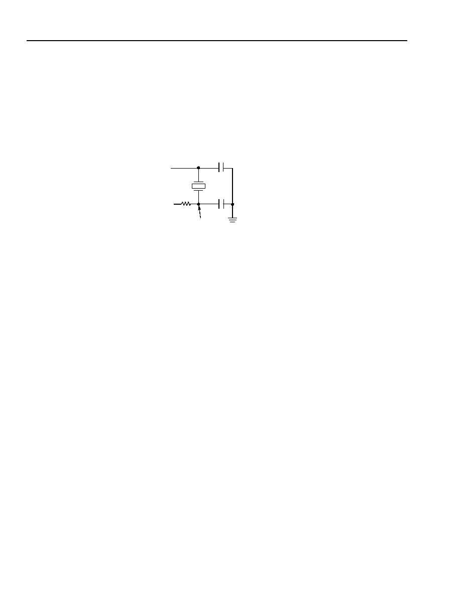
Figure 5. Crystal Circuitry
Adjustment to Crystal Loading
The resistor (R
L
) in Figure 5 is recommended for fine-tuning the crystal circuit. The value for this resistor is depen-
dent on the specific crystal used. Please refer to your crystal manufacturer's data sheet and application notes to
determine an appropriate value for R
L
. A more precise value for this resistor can be obtained by placing different
values of R
L
on a production board and using an oscilloscope to view the resultant clock waveform at node A for
each resistor value. The desired waveform should have the following characteristics: the waveform should be sinu-
soidal, with an amplitude as large as possible but not greater than 3.3 V or less than 0 volts.
Crystal/Board Layout
The layout of the crystal portion of the PHY circuit is important for obtaining the correct frequency and minimizing
noise introduced into the FW801BF PLL. The crystal and two load capacitors (C
A
+ C
B
) should be considered as a
unit during layout. They should be placed as close as possible to one another, while minimizing the loop area cre-
ated by the combination of the three components. Minimizing the loop area minimizes the effect of the resonant
current that flows in this resonant circuit. This layout unit (crystal and load capacitors) should then be placed as
close as possible to the PHY XI and XO terminals to minimize trace lengths. Vias should not be used to route the
XI and XO signals.
1394 Application Support Contact Information
E-mail: support1394@agere.com
A
C
B
C
A
X
I
X
O
R
L

Agere Systems Inc.
13
Data Sheet
January 2005
One-Cable Transceiver/Arbiter Device
FW801BF PHY 1394a-2000
Absolute Maximum Ratings
Stresses in excess of the absolute maximum ratings can cause permanent damage to the device. These are abso-
lute stress ratings only. Functional operation of the device is not implied at these or any other conditions in excess
of those given in the operational sections of the data sheet. Exposure to absolute maximum ratings for extended
periods can adversely affect device reliability.
Table 3. Absolute Maximum Ratings
* Except for 5 V tolerant I/O (CTL0, CTL1, D0--D7, and LREQ) where V
I
max = 5.5 V.
Parameter
Symbol
Min
Max
Unit
Supply Voltage Range
V
DD
3.0
3.6
V
Input Voltage Range*
V
I
≠0.5
V
DD
+ 0.5
V
Output Voltage Range at Any Output
V
O
≠0.5
V
DD
+ 0.5
V
Operating Free Air Temperature
T
A
0
70
∞
C
Storage Temperature Range
T
stg
≠65
150
∞
C

14
Agere Systems Inc.
Data Sheet
January 2005
One-Cable Transceiver/Arbiter Device
FW801BF PHY 1394a-2000
Electrical Characteristics
Table 4. Analog Characteristics
Parameter
Test Conditions
Symbol
Min
Typ
Max
Unit
Supply Voltage
Source power node
V
DD--SP
3.0
3.3
3.6
V
Differential Input Voltage
Cable inputs, 100 Mbits/s operation
V
ID--100
142
--
260
mV
Cable inputs, 200 Mbits/s operation
V
ID--200
132
--
260
mV
Cable inputs, 400 Mbits/s operation
V
ID--400
100
--
260
mV
Cable inputs, during arbitration
V
ID--ARB
168
--
265
mV
Common-mode Voltage
Source Power Mode
TPB cable inputs,
speed signaling off
V
CM
1.165
--
2.515
V
TPB cable inputs,
S100 speed signaling on
V
CM--SP--100
1.165
--
2.515
V
TPB cable inputs,
S200 speed signaling on
V
CM--SP--200
0.935
--
2.515
V
TPB cable inputs,
S400 speed signaling on
V
CM--SP--400
0.532
--
2.515
V
Common-mode Voltage
Nonsource Power Mode*
* For a node that does not source power (see Section 4.2.2.2 in IEEE 1394-1995 Standard).
TPB cable inputs,
speed signaling off
V
CM
1.165
--
2.015
V
TPB cable inputs,
S100 speed signaling on
V
CM--NSP--100
1.165
--
2.015
V
TPB cable inputs,
S200 speed signaling on
V
CM--NSP--200
0.935
--
2.015
V
TPB cable inputs,
S400 speed signaling on
V
CM--NSP--400
0.532
--
2.015
V
Receive Input Jitter
TPA, TPB cable inputs,
100 Mbits/s operation
--
--
--
1.08
ns
TPA, TPB cable inputs,
200 Mbits/s operation
--
--
--
0.5
ns
TPA, TPB cable inputs,
400 Mbits/s operation
--
--
--
0.315
ns
Receive Input Skew
Between TPA and TPB cable inputs,
100 Mbits/s operation
--
--
--
0.8
ns
Between TPA and TPB cable inputs,
200 Mbits/s operation
--
--
--
0.55
ns
Between TPA and TPB cable inputs,
400 Mbits/s operation
--
--
--
0.5
ns
Positive Arbitration
Comparator Input
Threshold Voltage
--
V
TH
+
89
--
168
mV
Negative Arbitration
Comparator Input
Threshold Voltage
--
V
TH
-
≠168
--
≠89
mV
Speed Signal Input
Threshold Voltage
200 Mbits/s
V
TH--S200
45
--
139
mV
400 Mbits/s
V
TH--S400
266
--
445
mV
Output Current
TPBIAS outputs
I
O
≠5
--
2.5
mA
TPBIAS Output Voltage
At rated I/O current
V
O
1.665
--
2.015
V
Current Source for
Connect Detect Circuit
--
I
CD
--
--
76
µ
A

Agere Systems Inc.
15
Data Sheet
January 2005
One-Cable Transceiver/Arbiter Device
FW801BF PHY 1394a-2000
Electrical Characteristics
(continued)
Table 5. Driver Characteristics
Parameter
Test Conditions
Symbol
Min
Typ
Max
Unit
Differential Output Voltage
56
load
V
OD
172
--
265
mV
Off-state Common-mode Voltage
Drivers disabled
V
OFF
--
--
20
mV
Driver Differential Current,
TPA, TPAN, TPB, TPBN
Driver enabled,
speed signaling off*
* Limits are defined as the algebraic sum of TPA+ and TPA
-
driver currents. Limits also apply to TPB+ and TPB
-
as the algebraic sum of driver
currents.
Limits are defined as the absolute limit of each of TPB+ and TPB
-
driver currents.
I
DIFF
≠1.05
--
1.05
mA
Common-mode Speed Signaling
Current, TPB, TPBN
200 Mbits/s speed
signaling enabled
I
SP
≠2.53
--
4.84
mA
400 Mbits/s speed
signaling enabled
I
SP
≠8.1
--
≠12.4
mA

16
Agere Systems Inc.
Data Sheet
January 2005
One-Cable Transceiver/Arbiter Device
FW801BF PHY 1394a-2000
Electrical Characteristics
(continued)
Table 6. Device Characteristics
* Device is capable of both differentiated and undifferentiated operation.
Parameter
Test Conditions
Symbol
Min
Typ
Max
Unit
Supply Current:
One Port Active
No Ports Active (Microlow-
power Sleep Mode), LPS = 0
PD = 1
V
DD
= 3.3 V
I
DD
I
DD
I
DD
--
--
--
54
50
50
--
--
--
mA
µ
A
µ
A
High-level Output Voltage
Electrical Character-
istics (continued)
I
OH
max, V
DD
= min
V
OH
V
DD
≠ 0.4
--
--
V
Low-level Output Voltage
I
OL
min, V
DD
= max
V
OL
--
--
0.4
V
High-level Input Voltage
CMOS inputs
V
IH
0.7 V
DD
--
--
V
Low-level Input Voltage
CMOS inputs
V
IL
--
--
0.2 V
DD
V
Pull-up Current,
RESETN Input
V
I
= 0 V
I
I
11
--
32
µ
A
Powerup Reset Time,
RESETN Input
V
I
= 0 V
--
2
--
--
ms
Rising Input Threshold Voltage
RESETN Input
--
VI
RST
1.1
--
1.4
V
Output Current
SYSCLK
I
OL
/I
OH
@ TTL
≠16
--
16
mA
Control, data
I
OL
/I
OH
@ CMOS
≠12
--
12
mA
CNA
I
OL
/I
OH
≠16
--
16
mA
C_LKON
I
OL
/I
OH
≠2
--
2
mA
Input Current,
LREQ, LPS, PD, SE, SM,
PC[0:2] Inputs
V
I
= V
DD
or 0 V
I
I
--
--
∞
±
1
µ
A
Off-state Output Current,
CTL[0:1], D[0:7], C_LKON I/Os
V
O
= V
DD
or 0 V
I
OZ
--
--
∞
±
5
µ
A
Power Status Input Threshold
Voltage, CPS Input
400 k
resistor
V
TH
7.5
--
8.5
V
Rising Input Threshold Voltage*,
LREQ, CTLn, Dn
--
V
IT
+
V
DD
/2 + 0.3
--
V
DD
/2 + 0.8
V
Falling Input Threshold Voltage*,
LREQ, CTLn, Dn
--
V
IT
-
V
DD
/2 ≠ 0.8
--
V
DD
/2 ≠ 0.3
V
Bus Holding Current,
LREQ, CTLn, Dn
V
I
= 1/2(V
DD
)
--
250
--
550
µ
A
Rising Input Threshold Voltage
LPS
--
V
LIH
--
--
0.24 V
DD
+ 1
V
Falling Input Threshold Voltage
LPS
--
V
LIL
0.24 V
DD
+ 0.2
--
--
V

Agere Systems Inc.
17
Data Sheet
January 2005
One-Cable Transceiver/Arbiter Device
FW801BF PHY 1394a-2000
Timing Characteristics
Table 7. Switching Characteristics
Table 8. Clock Characteristics
Symbol
Parameter
Measured
Test Conditions
Min
Typ
Max Unit
--
Jitter, Transmit
TPA, TPB
--
--
--
0.15
ns
--
Transmit Skew
Between
TPA and TPB
--
--
--
±
0.1
ns
t
r
Rise Time, Transmit (TPA/TPB)
10% to 90%
R
I
= 56
,
C
I
= 10 pF
--
--
1.2
ns
t
f
Fall Time, Transmit (TPA/TPB)
90% to 10%
R
I
= 56
,
C
I
= 10 pF
--
--
1.2
ns
t
su
Setup Time,
Dn, CTLn, LREQ
to SYSCLK
50% to 50%
See Figure .
6
--
--
ns
t
h
Hold Time,
Dn, CTLn, LREQ
from SYSCLK
50% to 50%
See Figure .
0
--
--
ns
t
d
Delay Time,
SYSCLK
to Dn, CTLn
50% to 50%
See Figure 7.
1
--
6
ns
Parameter
Symbol
Min
Typ
Max
Unit
External Clock Source Frequency
f
24.5735
24.5760
24.5785
MHz
18
Agere Systems Inc.
Data Sheet
January 2005
One-Cable Transceiver/Arbiter Device
FW801BF PHY 1394a-2000
Timing Waveforms
5-6017.a (F)
Figure 6. Dn, CTLn, and LREQ Input Setup and Hold Times Waveforms
5-6018.a (F)
Figure 7. Dn, CTLn Output Delay Relative to SYSCLK Waveforms
SYSCLK
Dn, CTLn, LREQ
tsu
th
SYSCLK
Dn, CTLn
td
Agere Systems Inc.
19
Data Sheet
January 2005
One-Cable Transceiver/Arbiter Device
FW801BF PHY 1394a-2000
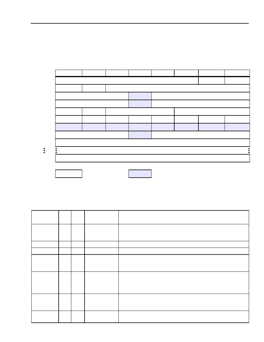
Internal Register Configuration
The PHY register map is shown below in Table 9. (Refer to IEEE 1394a-2000, 5B.1 for more information.)
Table 9. PHY Register Map for the Cable Environment
The meanings of the register fields within the PHY register map are defined by Table 10 below. Power reset values
not specified are resolved by the operation of the PHY state machines subsequent to a power reset.
Table 10. PHY Register Fields for the Cable Environment
Address
Contents
Bit 0
Bit 1
Bit 2
Bit 3
Bit 4
Bit 5
Bit 6
Bit 7
0000
2
Physical_ID
R
PS
0001
2
RHB
IBR
Gap_count
0010
2
Extended (7)
XXXXX
Total_ports
0011
2
Max_speed
XXXXX
Delay
0100
2
LCtrl
Contender
Jitter
Pwr_class
0101
2
Watchdog
ISBR
Loop
Pwr_fail
Timeout
Port_event Enab_accel Enab_multi
0110
2
XXXXX XXXXX XXXXX XXXXX XXXXX XXXXX XXXXX XXXXX
0111
2
Page_select
XXXXX
Port_select
1000
2
Register 0
Page_select
1111
2
Register 7
Page_select
REQUIRED
XXXXX
RESERVED
Field
Size Type
Power Reset
Value
Description
Physical_ID
6
r
000000
The address of this node determined during self-identification. A
value of 63 indicates a malconfigured bus; the link will not transmit
any packets.
R
1
r
0
When set to one, indicates that this node is the root.
PS
1
r
--
Cable power active.
RHB
1
rw
0
Root hold-off bit. When set to one, the force_root variable is TRUE,
which instructs the PHY to attempt to become the root during the
next tree identify process.
IBR
1
rw
0
Initiate bus reset. When set to one, instructs the PHY to set ibr
TRUE and reset_time to RESET_TIME. These values in turn
cause the PHY to initiate a bus reset without arbitration; the reset
signal is asserted for 166
µ
s. This bit is self-clearing.
Gap_count
6
rw
3F
16
Used to configure the arbitration timer setting in order to optimize
gap times according to the topology of the bus. See Section 4.3.6
of IEEE Standard 1394a-2000 for the encoding of this field.
Extended
3
r
111
This field has a constant value of seven, which indicates the
extended PHY register map.

20
Agere Systems Inc.
Data Sheet
January 2005
One-Cable Transceiver/Arbiter Device
FW801BF PHY 1394a-2000
Internal Register Configuration
(continued)
Table 10. PHY Register Fields for the Cable Environment (continued)
Field
Size Type Power Reset Value
Description
Total_ports
4
r
0001
The number of ports implemented by this PHY. This count
reflects the number.
Max_speed
3
r
010
Indicates the speed(s) this PHY supports:
000
2
= 98.304 Mbits/s
001
2
= 98.304 and 196.608 Mbits/s
010
2
= 98.304, 196.608, and 393.216 Mbits/s
011
2
= 98.304, 196.608, 393.216, and 786.43 Mbits/s
100
2
= 98.304, 196.608, 393.216, 786.432, and
1,572.864 Mbits/s
101
2
= 98.304, 196.608, 393.216, 786.432, 1,572.864, and
3,145.728 Mbits/s
All other values are reserved for future definition.
Delay
4
r
0000
Worst-case repeater delay, expressed as 144 + (delay * 20) ns.
LCtrl
1
rw
1
Link active. Cleared or set by software to control the value of
the L bit transmitted in the node's self-ID packet 0, which will be
the logical AND of this bit and LPS active.
Contender
1
rw
See description.
Cleared or set by software to control the value of the C bit trans-
mitted in the self-ID packet. Powerup reset value is set by
C_LKON ball.
Jitter
3
r
000
The difference between the fastest and slowest repeater data
delay, expressed as (jitter + 1) * 20 ns.
Pwr_class
3
rw
100
Power class. Controls the value of the pwr field transmitted in
the self-ID packet. See Section 4.3.4.1 of IEEE Standard
1394a-2000 for the encoding of this field.
Watchdog
1
rw
0
When set to one, the PHY will set Port_event to one if resume
operations commence for any port.
ISBR
1
rw
0
Initiate short (arbitrated) bus reset. A write of one to this bit
instructs the PHY to set ISBR true and reset_time to
SHORT_RESET_TIME. These values in turn cause the PHY to
arbitrate and issue a short bus reset. This bit is self-clearing.
Loop
1
rw
0
Loop detect. A write of one to this bit clears it to zero.
Pwr_fail
1
rw
1
Cable power failure detect. Set to one when the PS bit changes
from one to zero. A write of one to this bit clears it to zero.
Timeout
1
rw
0
Arbitration state machine timeout. A write of one to this bit
clears it to zero (see MAX_ARB_STATE_TIME).
Port_event
1
rw
0
Port event detect. The PHY sets this bit to one if any of con-
nected, bias, disabled, or fault change for a port whose
Int_enable bit is one. The PHY also sets this bit to one if
resume operations commence for any port and Watchdog is
one. A write of one to this bit clears it to zero.
Agere Systems Inc.
21
Data Sheet
January 2005
One-Cable Transceiver/Arbiter Device
FW801BF PHY 1394a-2000
Internal Register Configuration
(continued)
Table 10. PHY Register Fields for the Cable Environment (continued)
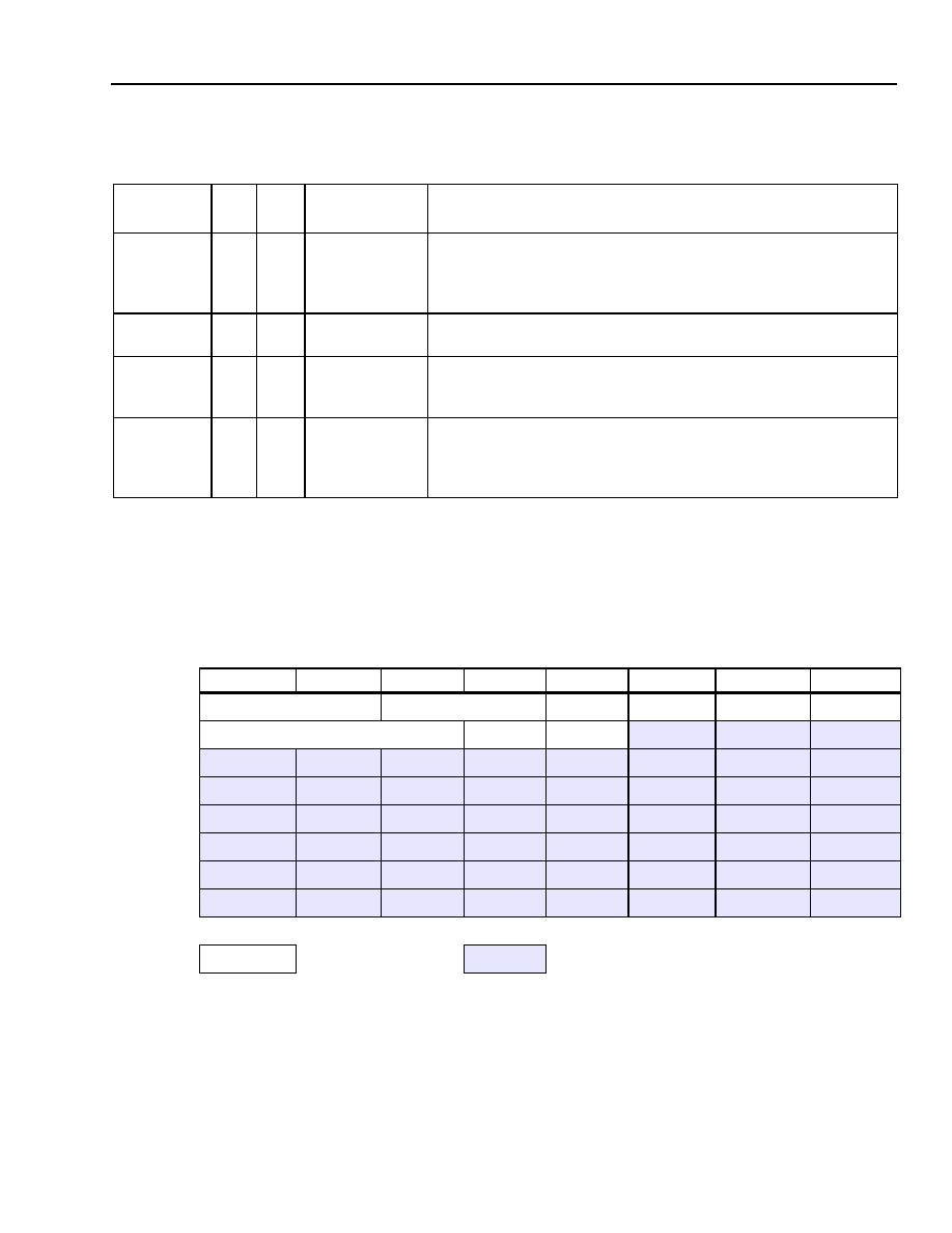
The port status page is used to access configuration and status information for each of the PHY's ports. The port is
selected by writing zero to Page_select and the desired port number to Port_select in the PHY register at address
0111
2
. The format of the port status page is illustrated by Table 11 below; reserved fields are shown shaded. The
meanings of the register fields with the port status page are defined by Table 12.
Table 11. PHY Register Page 0: Port Status Page
Field
Size Type
Power Reset
Value
Description
Enab_accel
1
rw
0
Enable arbitration acceleration. When set to one, the PHY will use
the enhancements specified in Section 4.4 of 1394a-2000 specifi-
cation. PHY behavior is unspecified if the value of Enab_accel is
changed while a bus request is pending.
Enab_multi
1
rw
0
Enable multispeed packet concatenation. When set to one, the link
will signal the speed of all packets to the PHY.
Page_select
3
rw
000
Selects which of eight possible PHY register pages are accessible
through the window at PHY register addresses 1000
2
through
1111
2
, inclusive.
Port_select
4
rw
0000
If the page selected by Page_select presents per-port information,
this field selects which port's registers are accessible through the
window at PHY register addresses 1000
2
through 1111
2
, inclusive.
Ports are numbered monotonically starting at zero, p0.
Address
Contents
Bit 0
Bit 1
Bit 2
Bit 3
Bit 4
Bit 5
Bit 6
Bit 7
1000
2
AStat
BStat
Child
Connected
Bias
Disabled
1001
2
Negotiated_speed
Int_enable
Fault
XXXXX XXXXX XXXXX
1010
2
XXXXX XXXXX XXXXX XXXXX XXXXX XXXXX XXXXX XXXXX
1011
2
XXXXX XXXXX XXXXX XXXXX XXXXX XXXXX XXXXX XXXXX
1100
2
XXXXX XXXXX XXXXX XXXXX XXXXX XXXXX XXXXX XXXXX
1101
2
XXXXX XXXXX XXXXX XXXXX XXXXX XXXXX XXXXX XXXXX
1110
2
XXXXX XXXXX XXXXX XXXXX XXXXX XXXXX XXXXX XXXXX
1111
2
XXXXX XXXXX XXXXX XXXXX XXXXX XXXXX XXXXX XXXXX
REQUIRED
XXXXX
RESERVED

22
Agere Systems Inc.
Data Sheet
January 2005
One-Cable Transceiver/Arbiter Device
FW801BF PHY 1394a-2000
Internal Register Configuration
(continued)
The meaning of the register fields with the port status page are defined by Table 12 below.
Table 12. PHY Register Port Status Page Fields
Field
Size Type
Power Reset
Value
Description
AStat
2
r
--
TPA line state for the port:
00
2
= invalid
01
2
= 1
10
2
= 0
11
2
= Z
BStat
2
r
--
TPB line state for the port (same encoding as AStat).
Child
1
r
0
If equal to one, the port is a child; otherwise, a parent. The
meaning of this bit is undefined from the time a bus reset is
detected until the PHY transitions to state T1: Child Hand-
shake during the tree identify process (see Section 4.4.2.2 in
IEEE Standard 1394-1995).
Connected
1
r
0
If equal to one, the port is connected.
Bias
1
r
0
If equal to one, incoming TPBIAS is detected.
Disabled
1
rw
0
If equal to one, the port is disabled.
Negotiated_speed
3
r
000
Indicates the maximum speed negotiated between this PHY
port and its immediately connected port; the encoding is the
same as for the PHY register Max_speed field.
Int_enable
1
rw
0
Enable port event interrupts. When set to one, the PHY will
set Port_event to one if any of connected, bias, disabled, or
fault (for this port) change state.
Fault
1
rw
0
Set to one if an error is detected during a suspend or resume
operation. A write of one to this bit clears it to zero.

Agere Systems Inc.
23
Data Sheet
January 2005
One-Cable Transceiver/Arbiter Device
FW801BF PHY 1394a-2000
Internal Register Configuration
(continued)
The vendor identification page is used to identify the PHY's vendor and compliance level. The page is selected by
writing one to Page_select in the PHY register at address 0111
2
. The format of the vendor identification page is
shown in Table 13; reserved fields are shown shaded.
Table 13. PHY Register Page 1: Vendor Identification Page
The meaning of the register fields within the vendor identification page are defined by Table 14.
Table 14. PHY Register Vendor Identification Page Fields
The vendor-dependent page provides access to information used in manufacturing test of the FW801BF.
Address
Contents
Bit 0
Bit 1
Bit 2
Bit 3
Bit 4
Bit 5
Bit 6
Bit 7
1000
2
Compliance_level
1001
2
XXXXX XXXXX XXXXX XXXXX XXXXX XXXXX XXXXX XXXXX
1010
2
1011
2
Vendor_ID
1100
2
1101
2
1110
2
Product_ID
1111
2
REQUIRED
XXXXX
RESERVED
Field
Size Type
Description
Compliance_level
8
r
Standard to which the PHY implementation complies:
0 = not specified.
1 = IEEE 1394a-2000.
Agere's FW801BF compliance level is 1.
All other values reserved for future standardization.
Vendor_ID
24
r
The company ID or organizationally unique identifier (OUI) of the manufacturer
of the PHY. Agere's vendor ID is 00601D
16
. This number is obtained from the
IEEE registration authority committee (RAC). The most significant byte of
Vendor_ID appears at PHY register location 1010
2
and the least significant at
1100
2
.
Product_ID
24
r
The meaning of this number is determined by the company or organization that
has been granted Vendor_ID. Agere's FW801BF product ID is 080201
16
. The
most significant byte of Product_ID appears at PHY register location 1101
2
and
the least significant at 1111
2
.
24
Agere Systems Inc.
Data Sheet
January 2005
One-Cable Transceiver/Arbiter Device
FW801BF PHY 1394a-2000
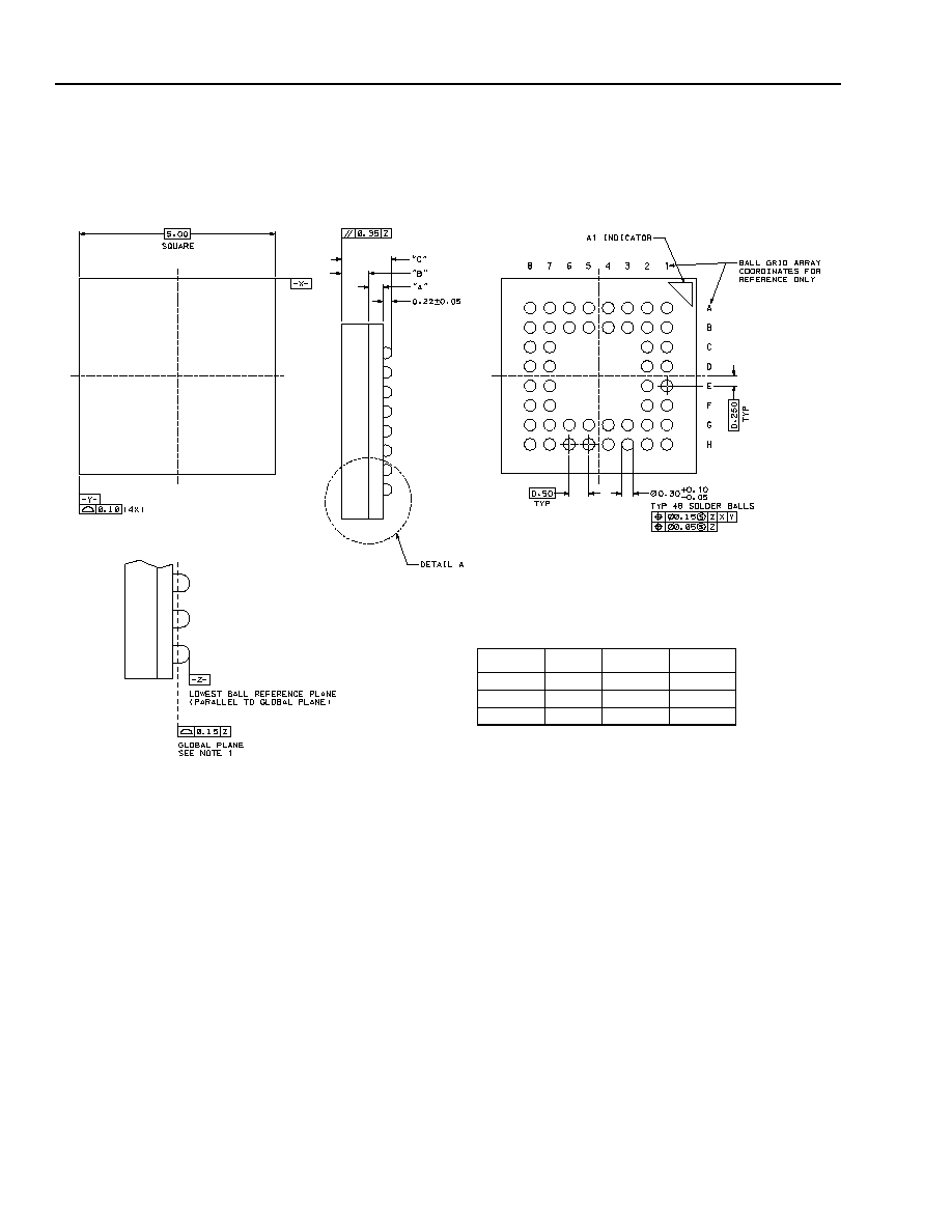
Outline Diagrams
48-Ball VTFSBGAC
Dimensions are in millimeters.
Note:
1. GLOBAL PLANE IS BEST FIT PLANE AS DETERMINED
BY COPLANARITY MEASUREMENT EQUIPMENT.
2. THIS PACKAGE CONFIGURATION HAS SOLDER MASK
DEFINED BGA PADS (SMD). FOR DETAILS SEE INDI-
VIDUAL SUBSTRATE DRAWINGS (BOTTOM VIEW).
3. THE SOLDER BALL DIAMETER BEFORE REFLOW =
0.30 mm +0.10/-0.05 mm.
PKG TYPE
A
B
C
FSBGA
0.36 REF 0.70 ± 0.05 1.28 ± 0.18
TFSBGA
0.21 REF 0.70 ± 0.05 1.13 ± 0.13
VTFSBGA
0.21 REf 0.45 ± 0.03 0.88 ± 0.10
DETAIL A
BOTTOM VIEW
TOP VIEW

Agere Systems Inc.
25
Data Sheet
January 2005
One-Cable Transceiver/Arbiter Device
FW801BF PHY 1394a-2000
Ordering Information
Device Code
Package
Comcode
FW801BF-09-DB
48-ball VTFSBGAC
7000482230

Agere Systems Inc. reserves the right to make changes to the product(s) or information contained herein without notice. No liability is assumed as a result of their use or application.
Agere is a registered trademark of Agere Systems Inc. Agere Systems and the Agere logo are trademarks of Agere Systems Inc.
Copyright © 2005 Agere Systems Inc.
All Rights Reserved
January 2005
DS05-043CMPR (Replaces DS03-080CMPR-2)
For additional information, contact your Agere Systems Account Manager or the following:
INTERNET:
http://www.agere.com
E-MAIL:
docmaster@agere.com
N. AMERICA: Agere Systems Inc., Lehigh Valley Central Campus, Room 10A-301C, 1110 American Parkway NE, Allentown, PA 18109-9138
1-800-372-2447, FAX 610-712-4106 (In CANADA: 1-800-553-2448, FAX 610-712-4106)
ASIA:
CHINA: (86) 21-54614688 (Shanghai), (86) 755-25881122 (Shenzhen)
JAPAN: (81) 3-5421-1600 (Tokyo), KOREA: (82) 2-767-1850 (Seoul), SINGAPORE: (65) 6741-9855, TAIWAN: (886) 2-2725-5858 (Taipei)
EUROPE:
Tel. (44) 1344 296 400
The i.LINK logo is a trademark and i.LINK is a registered trademark of Sony Corporation.
IEEE is a registered trademark of The Institute of Electrical and Electronics Engineers, Inc.
The FireWire logo is a trademark and FireWire is a registered trademark of Apple Computer, Inc.