 | –≠–ª–µ–∫—Ç—Ä–æ–Ω–Ω—ã–π –∫–æ–º–ø–æ–Ω–µ–Ω—Ç: L8574D | –°–∫–∞—á–∞—Ç—å:  PDF PDF  ZIP ZIP |
Document Outline
- Features
- Description
- List of Tables
- Table 1. Pin Descriptions
- Table 2. Operating Conditions and Powering
- Table 3. Ring Trip Detector
- Table 4. Battery Feed
- Table 5. Electrical Characteristics of Pins PT, PR, and VBF
- Table 6. Loss of Power Supplies
- Table 7. Analog Signal Pins
- Table 8. ac Transmission Characteristics
- Table 9. Logic Inputs (CE, CS, and B0-B3) and Output NSTAT
- Table 10. Timing Requirements (0-B3 and CS)
- Table 11. Relay Driver (RDO)
- Table 12. Battery Switch (SW1) and Ring Break Switch (SW2)
- Table 13. Ringing Access Switch (SW3)
- Table 14. Input State Coding
- Table 15. External Components Required
- Table 16. MMC A31A8574AA and MMC A11A8574AA Module
- List of Figures
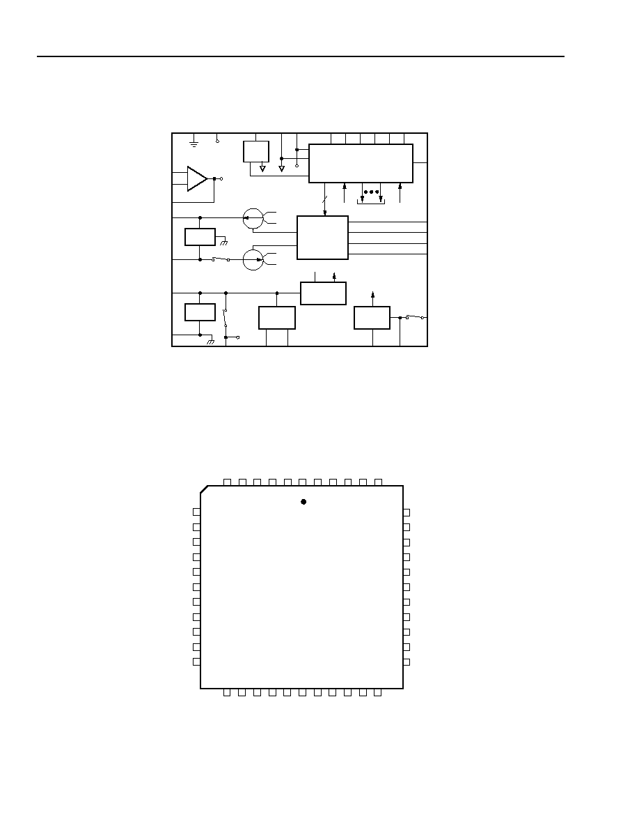
- Figure 1. Architectural Diagram
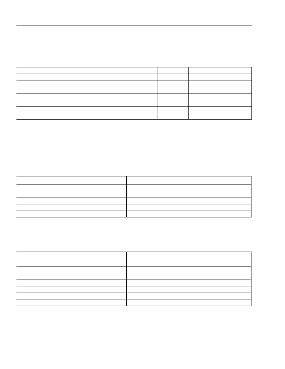
- Figure 2. Pin Layout
- Figure 3. Switch On-State V-I Characteristics SW1 and SW2
- Figure 4. Switch On-State V-I Characteristics SW3
- Figure 5. External Components Required
- Figure 6. Resistor Network
- Figure 7. L8574 SLIC Matching Requirements
- Figure 8. Implementing the Noise Cancellation Function
- Figure 9. Ring Trip Threshold
- Figure 10. Loop Current vs. Loop Voltage
- Figure 11. Equivalent Complex Terminations
- Figure 12. Initial ac Interface for Complex Termination Between L8574 SLIC and T7504 Codec
- Figure 13. Revised ac Interface CT and CR Combined into a Single Capacitor CS
- Figure 14. Addition of Resistor RSC from XMT to IRP
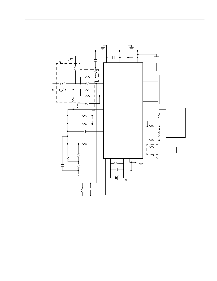
- Figure 15. TR-57 Application Diagram
- Architectural Diagram
- Pin Information
- Absolute Maximum Ratings
- Electrical Characteristics
- Operating States
- Applications
- dc Characteristics
- ac Design
- Application Diagram
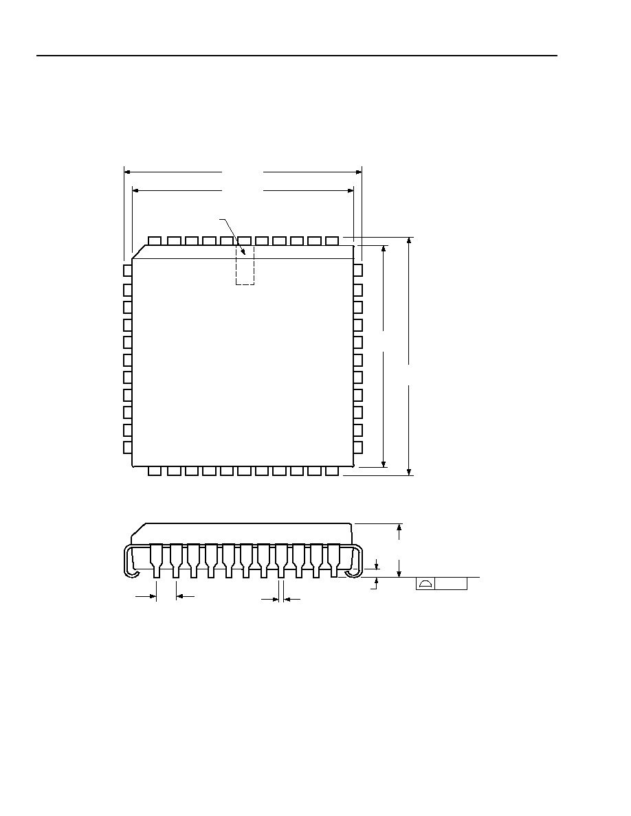
- Outline Diagram
- Ordering Information
- Contact Us

Data Sheet
October 1998
L8574D Resistive Subscriber Line Interface Circuit (SLIC), Ring
Relay, and Protector (SRP) for Long Loop and TR-57 Applications
Features
s
Low-power scan mode for low on-hook power dis-
sipation (55 mW max)
s
Low active power dissipation; talk or on-hook
transmission (240 mW max)
s
Distortion-free on-hook transmission
s
Eight operating states via latched paralleled data
inputs with channel select feature
s
Precision fixed 28 mA current limiter
s
Integrated protection
s
No external protection device required
s
Integrated ringing access relay
s
Ring trip detector
s
Loop closure detector with hysteresis
s
Relay driver
s
Battery noise cancellation
s
Thermal protection
s
44-pin, surface-mount, plastic package (PLCC)
Description
The L8574 is a resistive subscriber line interface cir-
cuit (SLIC) that is optimized for long loop applica-
tions, such as Bellcore TR-NWT-000057
requirements for digital loop carrier (DLC) applica-
tions. It interfaces the low-voltage circuits on an ana-
log line card to the Tip/Ring subscriber loop. The
L8574 does not supply dc current to the subscriber
loop; external resistors are used for this purpose.
Included in the L8574 are a solid-state ringing
access switch and a line break switch. Also included
is a relay driver for an external (test) access mechan-
ical relay.
State control is via four latched parallel data inputs. A
chip select feature allows the user to enable, disable,
or reset the data latches to a known logic state.
The L8574 offers a low-power scan state to minimize
power to less than 55 mW in the on-hook state. The
L8574 also supports on-hook transmission. The
active power in both the talk or on-hook transmission
mode is also very low (<240 mW). Current is limited
to a fixed value of 25 mA by an internal precision
current-limit circuit.
Because of the internal architecture of the L8574
SLIC and because of the power rating of the associ-
ated external feed resistors, the L8574 will meet most
surge requirements without use of an external sec-
ondary protection device. Internal circuitry steers
both positive and negative faults to fault ground. Neg-
ative faults are not dumped into battery.
The L8574 is a two-chip line interface solution pack-
aged in a single, 44-pin PLCC package. The Tip and
Ring drive amplifiers, the XMT amplifier, the receive
interface, and battery noise cancellation circuits are
fabricated in a 90 V complementary bipolar (CBIC)
process. The ring access switch, line break switch,
battery switch, current-limit, protection functions,
supervision, and control functions are fabricated in a
320 V dielectrically isolated bipolar-CMOS-DMOS
(BCDMOS) process. The device is available in a
44-pin PLCC package.

2
Lucent Technologies Inc.
Data Sheet
October 1998
Relay, and Protector (SRP) for Long Loop and TR-57 Applications
L8574D Resistive Subscriber Line Interface Circuit (SLIC), Ring
Table of Contents
Contents
Page
Features .................................................................................................................................................................... 1
Description ................................................................................................................................................................ 1
Architectural Diagram ................................................................................................................................................ 4
Pin Information .......................................................................................................................................................... 4
Absolute Maximum Ratings....................................................................................................................................... 6
Electrical Characteristics ........................................................................................................................................... 7
Ring Trip Detector ................................................................................................................................................... 8
Battery Feed ........................................................................................................................................................... 8
Fault Protection ....................................................................................................................................................... 9
Transmission Characteristics ................................................................................................................................ 13
Data Interface and Logic ....................................................................................................................................... 14
Switch Characteristics........................................................................................................................................... 15
Operating States...................................................................................................................................................... 16
Scan State ............................................................................................................................................................ 16
Disconnect State................................................................................................................................................... 17
Alternate Talk State ............................................................................................................................................... 17
Talk State .............................................................................................................................................................. 17
Scan Current-Limit State....................................................................................................................................... 17
Ringing State ........................................................................................................................................................ 17
On-Hook Transmission State ................................................................................................................................ 17
Intermediate Talk State ......................................................................................................................................... 18
Applications ............................................................................................................................................................. 18
General ................................................................................................................................................................. 18
Resistor Module .................................................................................................................................................... 22
Protection.............................................................................................................................................................. 24
Tip/Ring Drivers .................................................................................................................................................... 25
Receive Interface .................................................................................................................................................. 25
Transmit Interface.................................................................................................................................................. 25
Battery Noise Cancellation ................................................................................................................................... 25
On-Hook Transmission.......................................................................................................................................... 26
Parallel Data Interface........................................................................................................................................... 26
Supervision ........................................................................................................................................................... 26
Off-Hook Detection ............................................................................................................................................... 26
Ring Trip ................................................................................................................................................................ 26
Thermal Shutdown................................................................................................................................................ 27
Relay Driver .......................................................................................................................................................... 27
Solid-State Ringing Access................................................................................................................................... 27
Battery Supplies.................................................................................................................................................... 27
dc Characteristics .................................................................................................................................................... 27
V-I Characteristics................................................................................................................................................. 27
Loop Length .......................................................................................................................................................... 28
ac Design................................................................................................................................................................. 28
Codec Features and Selection Summary ............................................................................................................. 28
Design Equations.................................................................................................................................................. 29
Application Diagram ................................................................................................................................................ 33
Outline Diagram....................................................................................................................................................... 34
44-Pin PLCC ......................................................................................................................................................... 34
Ordering Information................................................................................................................................................ 35

Lucent Technologies Inc.
3
Data Sheet
October 1998
Relay, and Protector (SRP) for Long Loop and TR-57 Applications
L8574D Resistive Subscriber Line Interface Circuit (SLIC), Ring
Table of Contents
(continued)
Tables
Page
Table 1. Pin Descriptions ........................................................................................................................................... 5
Table 2. Operating Conditions and Powering ............................................................................................................ 7
Table 3. Ring Trip Detector ........................................................................................................................................ 8
Table 4. Battery Feed ................................................................................................................................................ 8
Table 5. Electrical Characteristics of Pins PT, PR, and V
BF
....................................................................................... 9
Table 6. Loss of Power Supplies.............................................................................................................................. 10
Table 7. Analog Signal Pins..................................................................................................................................... 11
Table 8. ac Transmission Characteristics................................................................................................................. 13
Table 9. Logic Inputs (CE, CS, and B0--B3) and Output NSTAT ............................................................................ 14
Table 10. Timing Requirements (B0--B3 and CS) .................................................................................................. 14
Table 11. Relay Driver (RDO) .................................................................................................................................. 14
Table 12. Battery Switch (SW1) and Ring Break Switch (SW2) .............................................................................. 15
Table 13. Ringing Access Switch (SW3) ................................................................................................................. 15
Table 14. Input State Coding ................................................................................................................................... 16
Table 15. External Components Required............................................................................................................... 20
Table 16.
MMC
A31A8574AA and
MMC
A11A8574AA Module.............................................................................. 23
Figures
Page
Figure 1. Architectural Diagram................................................................................................................................. 4
Figure 2. Pin Layout .................................................................................................................................................. 4
Figure 3. Switch On-State V-I Characteristics SW1 and SW2................................................................................. 16
Figure 4. Switch On-State V-I Characteristics SW3................................................................................................. 16
Figure 5. External Components Required ............................................................................................................... 19
Figure 6. Resistor Network ...................................................................................................................................... 23
Figure 7. L8574 SLIC Matching Requirements ....................................................................................................... 24
Figure 8. Implementing the Noise Cancellation Function ........................................................................................ 25
Figure 9. Ring Trip Threshold .................................................................................................................................. 26
Figure 10. Loop Current vs. Loop Voltage ............................................................................................................... 28
Figure 11. Equivalent Complex Terminations .......................................................................................................... 29
Figure 12. Initial ac Interface for Complex Termination Between L8574 SLIC and T7504 Codec .......................... 30
Figure 13. Revised ac Interface C
T
and C
R
Combined into a Single Capacitor C
S
................................................. 31
Figure 14. Addition of Resistor R
SC
from XMT to IRP ............................................................................................. 31
Figure 15. TR-57 Application Diagram .................................................................................................................... 33

4
Lucent Technologies Inc.
Data Sheet
October 1998
Relay, and Protector (SRP) for Long Loop and TR-57 Applications
L8574D Resistive Subscriber Line Interface Circuit (SLIC), Ring
Architectural Diagram
12-3330.a (C)r2
Figure 1. Architectural Diagram
Pin Information
12-3383.a (F)
Figure 2. Pin Layout
+5 A
V
BAT1
TIP CURRENT
DRIVER
+
≠
AX
V
XMT
RELAY
DRIVER
RDO
V
CCA
AGND
+5 A
+5 D
DGND V
DD
CE
CS
B0
B1
B2
B3
DATA INTERFACE,
LATCHES, AND LOGIC
2
NLC
SWITCH
CONTROL
NRT
RECEIVE
INTERFACE &
BATTERY NOISE
CANCELLATION
+5 A
V
BAT1
RING CURRENT
DRIVER
PROTECT
SW2
50
PROTECT
FGND
V
BF
V
BAT1
V
BAT1
CURRENT
LIMITER
V
BAT2
CLIM
SWITCHHOOK
DETECTOR
V
XMT
NLC
NRT
RING TRIP
DETECTOR
SW1
50
RTS
RSW
SW3
GTO
V
RNG
CBN
RGBN
RCVN
IRCV
NSTAT
1
2
3
4
5
6
7
8
9
10
11
12
13
14
15
16
17
18
19
20
21
22
23
24
25
26
27
28
29
30
31
32
33
34
35
36
37
38
39
40
41
42
43
44
L8574
XMT
TS
RS
RCVN
IRCV
V
CCA
CBN
RGBN
A
GND
PRA
NC
PRB
NSTAT
CS
NC
B2
B1
B0
CE
V
DD
DGND
RDO
RT
S
RSW
V
RNG
V
BA
T1
NC
V
BF
FGND
NC
PR
PT
NC
CLIM
V
BAT2
AGND
V
CCA
NC
PTA
NC
NC
B3
V
BA
T1
NC

Lucent Technologies Inc.
5
Data Sheet
October 1998
Relay, and Protector (SRP) for Long Loop and TR-57 Applications
L8574D Resistive Subscriber Line Interface Circuit (SLIC), Ring
Pin Information
(continued)
Table 1. Pin Descriptions
Pin
Symbol
Type
Name/Function
1
IRCV
I
Receive Signal Input (+).
The differential current flowing from PT to PR is
200 times the current flowing into IRCV.
2
V
CCA
--
+5 V Analog dc Supply.
+5 V supply for analog circuitry.
3
CBN
I
Battery Noise Capacitor.
The current flowing out of PR is ≠100 times the voltage
applied to CBN divided by the impedance connected between RGBN and AGND.
Connect a capacitor from CBN to V
BF
to eliminate battery noise from the Tip/Ring.
4
RGBN
I
Battery Noise Gain Resistor.
The current flowing out of PR is 100 times the cur-
rent flowing into RGBN. Connect a resistor from RGBN to AGND to set the gain of
the battery noise cancellation circuit.
5
AGND
--
Analog Ground.
Ground return for analog circuitry.
7
PRA
--
Protected Ring A.
Connect to PRB via an external coupling network.
8
PRB
--
Protected Ring B.
Connect to PRA via an external coupling network.
9
NSTAT
O
Not Status.
When low, this logic output indicates either a ring trip or an off-hook
condition, depending on the input state of the SLIC.
11
CS
I
Channel Select.
A low-to-high transition on this logic input stores the data on pins
B0--B3 into the input latches on the SLIC.
12
B3
I
Bit 3.
B0--B3 determine the state of the SLIC. See the Operating States section.
13
B2
I
Bit 2.
B0--B3 determine the state of the SLIC. See the Operating States section.
14
B1
I
Bit 1.
B0--B3 determine the state of the SLIC. See the Operating States section.
15
B0
I
Bit 0.
B0--B3 determine the state of the SLIC. See the Operating States section.
16
CE
I
Channel Enable.
A low on this logic input resets latches B0--B3 to the 1111 state
and disables the channel select input CS. A high on this logic input enables the
channel select input CS.
17
V
DD
--
+5 V Digital dc Supply.
+5 V supply for logic and switch circuitry.
18
DGND
--
Digital Ground.
Ground return for V
DD
and the relay driver.
19
RDO
O
Relay Driver.
This output drives an external relay.
20
RTS
I
Ring Trip Sense.
Sense input for the ring trip detector.
21
RSW
O
Ringing Access Switch.
Ringing relay connects this pin to pin V
RNG
(ringing sup-
ply). Connect this pin to pin V
BF
through a 600
current-limiting resistor.
22
V
RNG
--
Ringing Supply Voltage.
Connect this pin to the ringing supply.
23
V
BAT1
--
Office Battery Supply.
Negative high-voltage power supply.
25
V
BF
--
Feed Resistor Battery Supply.
Negative battery and ringing supply for the loop.
Connect this pin to the Ring of the loop through a 200
battery feed resistor.
27
FGND
--
Fault Ground.
30
PR
I/O
Protected Ring.
The input to the Ring fault protection and output of Ring current
drive amplifier (via the Ring access switch). Connect this pin to the Ring of the loop
through a 1 k
overvoltage protection resistor.
31
PT
I/O
Protected Tip.
The input to the Tip fault protection and output of Tip current drive
amplifier. Connect this pin to the Tip of the loop through a 1 k
overvoltage protec-
tion resistor. Connect to PTA via an external coupling network.

6
Lucent Technologies Inc.
Data Sheet
October 1998
Relay, and Protector (SRP) for Long Loop and TR-57 Applications
L8574D Resistive Subscriber Line Interface Circuit (SLIC), Ring
Pin Information
(continued)
Table 1. Pin Descriptions
(continued)
On the printed-wiring board (PWB), make the leads to FGND and V
BF
as wide as possible for thermal and electrical
reasons. Also, maximize the amount of PWB copper on all leads connected to this device for the lowest operating
temperature.
Absolute Maximum Ratings
(@ T
A
= 25
∞
C)
Stresses in excess of the absolute maximum ratings can cause permanent damage to the device. These are abso-
lute stress ratings only. Functional operation of the device is not implied at these or any other conditions in excess
of those indicated in the operational sections of this data sheet. Exposure to absolute maximum ratings for
extended periods can adversely affect device reliability.
Notes:
Analog voltages (V
CCA
, V
BAT1
, and V
BAT2
) are referenced to AGND, and digital (logic) voltages (V
DD
) are referenced to DGND.
The IC can be damaged unless all ground connections are applied before, and removed after, all other connections. Furthermore, when power-
ing the device, the user must guarantee that no external potential creates a voltage on any pin of the device that exceeds the device ratings. For
example, inductance in a supply lead could resonate with the supply filter capacitor to cause a destructive overvoltage.
Pin
Symbol
Type
Name/Function
33
CLIM
I
Current Limiter Capacitor.
Connect a 0.1
µ
F capacitor from this pin to pin V
BF
.
34
V
BAT2
--
Office Battery Supply.
Negative high-voltage power supply.
35
AGND
--
Analog Ground.
Ground return for analog circuitry.
36
V
CCA
--
+5 V Analog dc Supply.
+5 V supply for analog circuitry.
38
PTA
--
Protected Tip A.
Connect to PT via an external coupling network.
40
V
BAT1
--
Office Battery Supply.
Negative high-voltage power supply.
41
XMT
O
Transmit Signal Output.
Transmit amplifier output to codec.
42
TS
I
Tip Sense.
Negative (≠) input of transmit op amp. Connect one high-value resis-
tor between TS and the Tip of the loop and another high-value resistor between
TS and XMT.
43
RS
I
Ring Sense.
Positive (+) input of the transmit op amp. Connect one high-value
resistor between RS and the Ring of the loop and another high-value resistor
between RS and AGND (see the application diagram, Figure 5).
44
RCVN
I
Receive Signal Input (≠). The differential current flowing from PT to PR is ≠200
times the voltage applied to RCVN divided by the impedance connected
between IRCV and AGND.
Parameter
Symbol
Min
Typ
Max
Unit
+5 V dc Supplies (V
CCA
& V
DD
)
--
≠0.5
--
7.0
V
Office Battery Supply
V
BAT1
V
BAT2
≠63
≠63
--
--
0.5
0.5
V
V
Logic Input Voltage
--
≠0.5
--
V
DD
+ 0.5
V
Logic Input Clamp Diode Current, per Pin
--
--
±
20
--
mA
Logic Output Voltage
--
≠0.5
--
V
DD
+ 0.5
V
Logic Output Current, per Pin (excluding relay driver)
--
--
±
35
--
mA
Operating Temperature Range
--
≠40
--
125
∞
C
Storage Temperature Range
T
stg
≠40
--
125
∞
C
Relative Humidity Range
--
5
--
95
%
Ground Potential Difference (DGND to AGND)
--
--
±
3
--
V

Lucent Technologies Inc.
7
Data Sheet
October 1998
Relay, and Protector (SRP) for Long Loop and TR-57 Applications
L8574D Resistive Subscriber Line Interface Circuit (SLIC), Ring
Electrical Characteristics
In general, minimum and maximum values are testing requirements. However, some parameters may not be
tested in production because they are guaranteed by design and device characterization. Typical values reflect
the design center or nominal value of the parameter; they are for information only and are not a requirement. Mini-
mum and maximum values apply across the entire temperature range (≠40
∞
C to +85
∞
C) and entire battery range
(≠35 V to ≠60 V). Unless otherwise specified, typical is defined as 25
∞
C, V
CCA
and V
DD
= +5.0 V, V
BAT1
and V
BAT2
=
≠48 V. Positive currents flow into the device.
Table 2. Operating Conditions and Powering
1. Not to exceed 26 grams of water per kilogram of dry air.
2. Includes current in all external resistors per Figure 15.
3. This parameter is not tested in production. It is guaranteed by design and device characterization.
4. V
BAT1
and V
BAT2
power supply rejection depends on the battery noise cancellation circuit. The performance stated here applies to V
BAT2
only
during the talk state and V
BAT1
only during the on-hook transmission state and assumes proper battery noise cancellation (see Figure 5).
Parameter
Min
Typ
Max
Unit
Temperature Range
≠40
--
85
∞
C
Humidity Range
5
--
95
1
%RH
Supply Voltages:
V
CCA
V
DD
V
BAT1
V
BAT2
V
CCA
≠ V
DD
4.6
4.6
≠42.5
≠20
--
5.0
5.0
≠48
≠48
--
5.5
5.5
≠60
V
BAT1
±
0.5
V
V
V
V
V
Supply Currents (scan state; no loop current)
2
:
I
VCCA
+ I
VDD
(+5 V)
I
VBAT1
(≠48 V) + I
VBAT2
(≠48 V)
--
--
--
--
3.0
≠825
mA
µ
A
Supply Currents (talk or on-hook transmission state; no loop current)
2
:
I
VCCA
+ I
VDD
(+5 V)
I
VBAT1
(≠48 V) + I
VBAT2
(≠48 V)
--
--
--
--
6.0
≠4.5
mA
mA
Total Power Dissipation (no loop current)
2
(V
CCA
and V
DD
= +5 V; V
BAT1
and V
BAT2
= ≠48 V):
Talk or On-hook Transmission State
Scan State
--
--
--
--
240
55
mW
mW
Power Supply Rejection (Tip/Ring)
3
:
V
CCA
(500 Hz--3 kHz; 50 mVrms ripple)
V
DD
(500 Hz--3 kHz; 50 mVrms ripple)
V
BAT2
and V
BAT1
(500 Hz--2 kHz; 50 mVrms ripple)
4
V
BAT2
and V
BAT1
(2 kHz--3 kHz; 50 mVrms ripple)
4
40
50
40
35
50
--
--
40
--
--
--
--
dB
dB
dB
dB
Thermal
3
:
Thermal Resistance (still air)
Operating T
jc
Thermal Shutdown Temperature
--
--
--
--
--
145
60
135
--
∞
C/W
∞
C
∞
C

8
Lucent Technologies Inc.
Data Sheet
October 1998
Relay, and Protector (SRP) for Long Loop and TR-57 Applications
L8574D Resistive Subscriber Line Interface Circuit (SLIC), Ring
Electrical Characteristics
(continued)
Ring Trip Detector
Table 3. Ring Trip Detector
1. The ringing source consists of the ac and dc voltages added together (battery-backed ringing); the ringing return is battery ground.
2. Pretrip: ringing must not be tripped by a 10 k
resistor in parallel with an 8
µ
F capacitor applied across Tip and Ring.
Battery Feed
Table 4. Battery Feed
1. Assumes 2 x 200
external dc feed resistors.
2. When the current-limit circuit is active and the battery switch is off, the longitudinal current must be less than the dc loop current to ensure
proper ac transmission.
3. Assumes C
LIM
= 33 nF; C
LIM
determines the ac output impedance of the current-limit circuit when it is active.
4. Detector values are independent of office battery and are valid over the entire range of V
BAT1
and V
BAT2
. However, NSTAT must indicate an
on-hook (NSTAT = 1) if either V
BAT1
or V
BAT2
is disconnected (open circuit) from its dc source and an off-hook (NSTAT = 0) if the L8574 is in
thermal shutdown. The status of the thermal shutdown circuit is output on B3 when CS is high (thermal shutdown is a logic 0). V
BAT1
and
V
BAT2
are defined as disconnected depending on the voltage at the power supply pins as follows (the pins of supplies that have more than
one pin are shorted together):
-- If V
BAT1
≠20 V (i.e., more negative than ≠20 V) and V
BAT2
≠20 V, then NSTAT must operate normally.
-- If V
BAT1
≠10 V (i.e., more positive than ≠10 V) or V
BAT2
≠10 V, then NSTAT must be on-hook (NSTAT = 1).
5.
IEEE is a registered trademark of The Institute of Electrical and Electronics Engineers, Inc.
6. Assumes the external dc feed resistors are matched to 0.2% and proper battery noise cancellation; i.e., a 0.22
µ
F capacitor from V
BF
to CBN
(see Figure 5).
7. Assumes proper battery noise cancellation; i.e., a 0.22
µ
F capacitor from V
BF
to CBN (see Figure 5).
Parameter
Min
Typ
Max
Unit
Ringing Source
1
:
Frequency (f)
dc Voltage
ac Voltage
17
≠36
60
20
--
--
28
≠57
105
Hz
V
Vrms
Ring Trip
2
(NSTAT = 0):
Loop Resistance
Trip Time (f = 20 Hz)
NSTAT Valid
1840
--
--
--
--
--
--
200
80
ms
ms
Parameter
Min
Typ
Max
Unit
Loop Resistance Range
1
(3.17 dBm overload into 600
):
I
LOOP
= 18 mA at V
BAT2
= ≠42 V
1840
--
--
Longitudinal Current Capability per Wire
2
8.5
--
--
mArms
dc Loop Current Limit (R
LOOP
= 200
)
26.5
28
29.5
mA
Current-limiter ac Output Impedance
3
:
200 Hz to 4 kHz
--
--
25
Current-limiter Transient Current (in response to a step voltage
change on V
BF
)
8
--
150
mA
Switchhook Detector Loop Resistance
4
:
Off-hook (NSTAT = 0)
On-hook (NSTAT = 1)
--
--
4400
3300
--
--
--
2700
--
Longitudinal to Metallic Balance--
IEEE
5
Std. 455
6
:
200 Hz to 1 kHz
1 kHz to 3 kHz
58
53
--
--
--
--
dB
dB
Metallic to Longitudinal (Harm) Balance
7
:
200 Hz to 4 kHz
30
--
--
dB

Lucent Technologies Inc.
9
Data Sheet
October 1998
Relay, and Protector (SRP) for Long Loop and TR-57 Applications
L8574D Resistive Subscriber Line Interface Circuit (SLIC), Ring
Electrical Characteristics
(continued)
Fault Protection
Pins PT, PR, and V
BF
Pins PT, PR, and V
BF
are protected by SCRs which clamp surge currents (both positive and negative) to FGND. If
the SCR on PR or V
BF
triggers due to a negative surge, the L8574 automatically switches to the disconnect state
while the SCR is conducting current above its hold current. After the SCR releases, the L8574 automatically
switches back to the operating state prior to the SCR trigger.
Table 5. Electrical Characteristics of Pins PT, PR, and V
BF
1. This parameter is not tested in production. It is guaranteed by design and device characterization.
2. Applied voltage is 50 Vpp square wave at 100 Hz to measure dV/dt sensitivity.
Parameter
Min
Typ
Max
Unit
PT and PR:
Surge Current
1
:
Lightning--10
µ
s x 1000
µ
s
Lightning--2
µ
s x 10
µ
s
Power Cross--60 Hz, 50 ms
Power Cross--60 Hz, 1 s
Power Cross--60 Hz, 15 min.
--
--
--
--
--
--
--
--
--
--
±
1
±
2.5
600
200
50
A
A
mArms
mArms
mArms
SCR Trigger Voltage Pin PT:
Positive
Negative
dc Transient Response
V
CCA
≠ 2
≠25
≠25
--
--
--
V
CCA
+ 4
≠35
≠55
V
V
V
SCR Trigger Voltage Pin PR:
Positive
Negative
150
≠220
--
--
280
320
V
V
SCR Hold Current (positive and negative)
10
--
--
mA
V
BF
:
Surge Current
1
:
Lightning--10
µ
s x 1000
µ
s
Lightning--2
µ
s x 10
µ
s
Power Cross--60 Hz, 50 ms
Power Cross--60 Hz, 1 s
Power Cross--60 Hz, 15 min.
--
--
--
--
--
--
--
--
--
--
±
5.5
±
13
3
800
150
A
A
Arms
mArms
mArms
SCR Trigger Voltage:
Positive
Negative
150
≠220
--
--
280
≠320
V
V
SCR Hold Current (positive and negative)
10
--
--
mA
Trigger Current (if from a power supply--PT, PR, and V
BF
)
--
--
±
250
µ
A
dV/dt Sensitivity
1, 2
(PT, PR, and V
BF
)
--
500
--
V/
µ
s

10
Lucent Technologies Inc.
Data Sheet
October 1998
Relay, and Protector (SRP) for Long Loop and TR-57 Applications
L8574D Resistive Subscriber Line Interface Circuit (SLIC), Ring
Electrical Characteristics
(continued)
Fault Protection
(continued)
Loss of Power Supplies
The L8574 must protect itself from lightning and power cross voltages on Tip and Ring if any (or any combination)
of the power supplies (V
CCA
, V
DD
, V
BAT1
, and V
BAT2
) are disconnected (open circuit) from their dc source. Addition-
ally, if any power supply is disconnected, no overvoltage on Tip or Ring can cause a supply voltage to exceed its
maximum rating. Under these conditions, V
CCA
and V
DD
are considered as one supply (V
CCA
shorted to V
DD
), the
pins of supplies which have more than one pin are shorted together, and bypass capacitors are connected. To sat-
isfy these requirements (and also to disconnect ringing from the loop when ring trip cannot be detected), the L8574
is placed into the disconnect state depending on the voltage at the power supply pins as shown in Table 6.
Table 6. Loss of Power Supplies
Parameter
Min
Typ
Max
Unit
V
CCA
and V
DD
:
Normal Operating State (as defined by control logic)
Disconnect State
1
--
--
--
--
4.5
V
V
V
BAT1
:
Normal Operating State (as defined by control logic)
Disconnect State
Disconnect State
≠10
--
≠65
--
--
--
≠75
≠20
--
V
V
V

Lucent Technologies Inc.
11
Data Sheet
October 1998
Relay, and Protector (SRP) for Long Loop and TR-57 Applications
L8574D Resistive Subscriber Line Interface Circuit (SLIC), Ring
Electrical Characteristics
(continued)
Fault Protection
(continued)
Loss of Power Supplies (continued)
Table 7. Analog Signal Pins
1. Connected per Figure 5.
2. A battery or ground short on PT, PR, or XMT shall not cause a device failure.
3. This parameter is not tested in production. It is guaranteed by design and device characterization.
Parameter
Min
Typ
Max
Unit
PT and PR:
Surge Current (See the Protection section.)
Output Drive (PT):
Drive Current
Negative Voltage Swing (I
OUT
+ 10 mA)
Positive Voltage Swing (I
OUT
≠ 10 mA)
dc Bias Current
±
15
V
BAT1
+ 4.5
V
CCA
≠ 3.5
600
--
--
--
--
--
V
BAT1
V
CCA
900
mA
V
V
µ
A
Output Drive (PR):
Positive (sink) Drive Current
Negative Voltage Swing (I
OUT
+ 10 mA)
Positive Voltage Swing (I
OUT
≠ 10 mA)
dc Bias Current (V
BAT2
= V
BAT1
≠ 48 V)
1
±
15
V
BAT1
+ 4.5
V
CCA
≠ 3.5
≠0.8
--
--
--
--
--
V
BAT1
V
CCA
≠1.4
mA
V
V
mA
Output Short-circuit Transient Current
2
Output Impedance (60 Hz--3.4 kHz)
3
Output Load Resistance (dc or ac)
3
Output Load Capacitance
3
--
250
100
--
--
--
--
--
±
125
--
--
1
mA
k
nF
XMT:
Output Drive Current
Output Voltage Swing (1 mA load):
Maximum
Minimum
Output Short-circuit dc Current
Output Impedance (60 Hz--3.4 kHz)
3
Output Load dc Resistance
3
Output Load ac Resistance
Output Load Capacitance
3
±
1
V
BAT1
V
BAT1
+ 5
--
--
50
2
--
--
--
--
--
--
--
--
--
--
V
CCA
2.5
±
20
10
--
--
50
mA
V
V
mA
k
k
pF

12
Lucent Technologies Inc.
Data Sheet
October 1998
Relay, and Protector (SRP) for Long Loop and TR-57 Applications
L8574D Resistive Subscriber Line Interface Circuit (SLIC), Ring
Electrical Characteristics
(continued)
Fault Protection
(continued)
Loss of Power Supplies (continued)
Table 7. Analog Signal Pins (continued)
1. Connected per Figure 5.
2. A battery or ground short on PT, PR, or XMT shall not cause a device failure.
3. This parameter is not tested in production. It is guaranteed by design and device characterization.
Parameter
Min
Typ
Max
Unit
RCVN:
Input Voltage Range
Input Bias Current
Input Impedance
3
≠1.75
--
20
--
--
--
V
CCA
≠ 1.0
±
1
--
V
µ
A
M
IRCV:
Input Offset Voltage (to RCVN)
Input Impedance
3
--
--
--
--
±
20
5
mV
CBN:
Surge Current (lightning 10
µ
s x 1000
µ
s)
Input Voltage Range
Input Bias Current
Input Impedance
3
Input Positive Clamp Voltage (I
CBN
= +100
µ
A)
Input Negative Clamp Voltage (I
CBN
= ≠100
µ
A)
--
≠1.75
--
50
1.50
≠2.00
--
--
--
--
--
--
±
100
1.25
±
250
--
1.90
≠3.20
mA
V
nA
M
V
V
RGBN:
Input Offset Voltage (to CBN)
Input Impedance
3
--
--
--
--
±
10
5
mV
TS and RS:
Surge Current from External Source
Input Voltage Range
3
Input Bias Current
Differential Input Impedance
3
Common-mode Input Impedance
3
External Capacitance (67 k
source impedance)
3
--
V
BAT1
+ 3
--
50
50
--
--
--
--
--
--
--
±
25
AGND
±
1
--
--
10
mAdc
V
µ
A
k
M
pF

Lucent Technologies Inc.
13
Data Sheet
October 1998
Relay, and Protector (SRP) for Long Loop and TR-57 Applications
L8574D Resistive Subscriber Line Interface Circuit (SLIC), Ring
Electrical Characteristics
(continued)
Transmission Characteristics
Transmit direction is Tip/Ring to XMT. Receive direction is IRCV/RCVN to Tip/Ring.
Table 8. ac Transmission Characteristics
1. Requires external components connected as shown in Figure 5. Transmission characteristics are specified assuming a 900
resistive ter-
mination and
±
1% external resistors.
2. Transmission characteristics are specified assuming a 900
resistive termination; however, feedback using external components allows the
user to adjust the termination impedance from 900
to most ITU-T recommended complex termination impedances.
3. This parameter is not tested in production. It is guaranteed by design and device characterization.
Parameter
1
Min
Typ
Max
Unit
ac Termination Impedance
2
--
600
--
Return Loss
3
:
200 Hz--500 Hz
500 Hz--2500 Hz
2500 Hz--3400 Hz
21
26
21
--
--
--
--
--
--
dB
dB
dB
Tip/Ring Signal Level (600
reference)
--
--
3.14
dBm
Total Harmonic Distortion (200 Hz--4 kHz)
3
--
--
0.3
%
Transmit Gain (f = 1 kHz):
(Tip/Ring) to XMT
≠0.486
≠0.500
≠0.514
--
Receive Gain (f = 1 kHz):
IRCV to Differential Current Flowing from IPT to IPR
RCVN to IRCV
195
0.995
200
1
205
1.005
--
--
Gain vs. Frequency (transmit and receive; 1 kHz reference)
3
:
200 Hz--300 Hz
300 Hz--3.4 kHz
3.4 kHz--20 kHz
20 kHz--266 kHz
≠1.00
≠0.30
≠3.0
--
0
0
0
--
0.05
0.05
1.0
1.0
dB
dB
dB
dB
Gain vs. Level (transmit and receive; 0 dBV reference)
3
:
≠50 dB to +3 dB
≠0.05
0
0.05
dB
Transhybrid Loss
3
:
200 Hz--500 Hz
500 Hz--2500 Hz
2500 Hz--3400 Hz
21
26
21
--
--
--
--
--
--
dB
dB
dB
Idle-channel Noise (Tip/Ring):
Psophometric
3
C-message
3 kHz Flat
3
--
--
--
--
--
--
≠77
12
20
dBmp
dBrnC
dBrn
Idle-channel Noise (XMT):
Psophometric
3
C-message
3 kHz Flat
3
--
--
--
--
--
--
≠77
12
20
dBmp0
dBrnC0
dBrn0

14
Lucent Technologies Inc.
Data Sheet
October 1998
Relay, and Protector (SRP) for Long Loop and TR-57 Applications
L8574D Resistive Subscriber Line Interface Circuit (SLIC), Ring
Electrical Characteristics
(continued)
Data Interface and Logic
Table 9. Logic Inputs (CE, CS, and B0--B3) and Output NSTAT
1. Unless otherwise specified, all logic voltages are referenced to DGND.
2. This parameter is not tested in production. It is guaranteed by design and device characterization.
Table 10. Timing Requirements (B0--B3 and CS)
A low-to-high transition on pin CS latches the data on pins B0--B3 into the device. When CS is either high or low,
the device is unaffected by data on pins B0--B3. The status of the thermal shutdown circuit is output on B3 when
CS is high (thermal shutdown is a logic 0). A low on channel enable lead CE asynchronously resets the data latch
to 1111 (scan state with the relay driver off) and disables CS so that CS cannot latch any data into the device. A
high on CE enables CS.
1. Unless otherwise specified, all times are measured from the 50% point of logic transitions.
2. These parameters are not tested in production. They are guaranteed by design and device characterization.
Table 11. Relay Driver (RDO)
The relay driver output RDO is low (relay operated) when a low input on B3 is latched into the device.
1. Unless otherwise specified, all logic voltages are referenced to DGND.
2. This parameter is not tested in production. It is guaranteed by design and device characterization.
Parameter
1
Symbol
Min
Max
Unit
High-level Input Voltage
V
IH
2
V
DD
V
Low-level Input Voltage
V
IL
0
0.8
V
Input Bias Current (high and low)
I
IN
--
±
10
µ
A
High-level Output Voltage (I
OUT
= ≠100
µ
A)
V
OH
V
DD
≠ 1.5
V
DD
V
Low-level Output Voltage (I
OUT
= 180
µ
A)
V
OL
0
0.4
V
Output Short-circuit Current (V
OUT
= V
DD
)
I
OSS
1
35
mA
Output Load Capacitance
2
C
OL
0
50
pF
Parameter
1, 2
Symbol
Min
Max
Unit
CS Rise and Fall Time (10% to 90%)
t
R
, t
F
0
50
ns
Maximum Input Capacitance
C
IN
--
5
pF
Minimum Setup Time from B0--B3 Valid to CS
t
SDS
150
--
ns
Minimum Hold Time from CS to B0--B3 Not Valid
t
HDS
50
--
ns
Minimum Pulse Width of CS
t
WCS
225
--
ns
Parameter
1
Symbol
Min
Max
Unit
Off-state Output Current (V
RDO
= V
DD
)
I
OFF
--
±
10
µ
A
On-state Output Voltage (I
RDO
= 70 mA)
V
ON
0
1.0
V
On-state Output Voltage (I
RDO
= 20 mA)
V
ON
0
0.40
V
Clamp Diode Reverse Current (V
RDO
= 0)
I
R
--
±
10
µ
A
Clamp Diode On Voltage (I
RDO
= 150 mA)
V
OC
V
DD
V
DD
+ 2.0
V
Turn-on Time
2
t
ON
--
10
µ
s
Turn-off Time
2
t
OFF
--
10
µ
s

Lucent Technologies Inc.
15
Data Sheet
October 1998
Relay, and Protector (SRP) for Long Loop and TR-57 Applications
L8574D Resistive Subscriber Line Interface Circuit (SLIC), Ring
Electrical Characteristics
(continued)
Switch Characteristics
Table 12. Battery Switch (SW1) and Ring Break Switch (SW2)
1. SW2 must be off if the voltage on pin PR is more positive than V
CCA
.
2. At 25
∞
C. Maximum voltage rating has a temperature coefficient of +0.167 V/
∞
C.
3. This parameter is not tested in production. It is guaranteed by design and device characterization.
4. Applied voltage is 100 Vpp square wave at 100 Hz to measure dV/dt sensitivity.
Table 13. Ringing Access Switch (SW3)
1. This parameter is not tested in production. It is guaranteed by design and device characterization.
2. Applied voltage is 100 Vpp square wave at 100 Hz to measure dV/dt sensitivity.
Parameter
Min
Typ
Max
Unit
Off-state
1
:
Maximum Differential Voltage
dc Leakage Current (V
SW
±
320 V)
Feedthrough Capacitance
3
--
--
--
--
--
--
±
320
2
±
50
50
V
µ
A
pF
On-state (See Figures 3 and 4.):
Resistance (R
ON
)
Maximum Differential Voltage (V
max
)
Current Limit (I
LIMIT
)
--
--
20
50
--
35
100
320
2
60
V
mA
dV/dt Sensitivity
3, 4
--
200
--
V/
µ
s
Parameter
Min
Typ
Max
Unit
Off-state:
Maximum Differential Voltage
dc Leakage Current (V
SW
=
±
500 V)
dc Leakage Current (V
SW
=
±
250 V)
Feedthrough Capacitance
1
--
--
--
--
--
--
--
--
±
500
±
20
±
1
10
V
µ
A
µ
A
pF
On-state (See Figures 3 and 4.):
Crossover Offset Voltage (V
OS
; I
SW
=
±
1 mA)
Resistance (R
ON
)
Surge Current (10
µ
s x 1000
µ
s pulse)
1
Release Current
1
--
--
--
0.1
--
--
--
--
3
10
2.0
3
V
A
mA
dV/dt Sensitivity
1, 2
--
500
--
V/
µ
s

16
16
Lucent Technologies Inc.
Data Sheet
October 1998
Relay, and Protector (SRP) for Long Loop and TR-57 Applications
L8574D Resistive Subscriber Line Interface Circuit (SLIC), Ring
Electrical Characteristics
(continued)
Switch Characteristics
(continued)
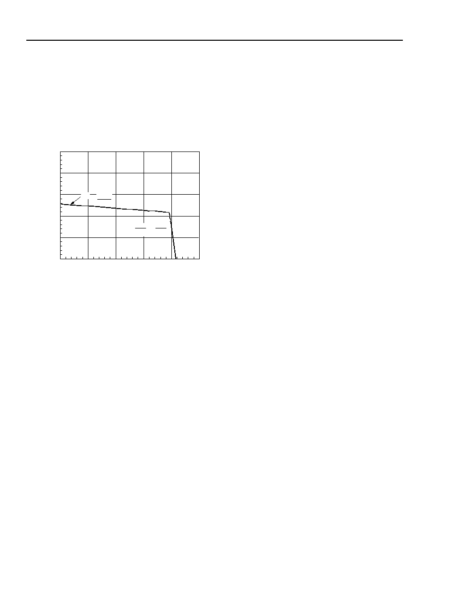
12-3332 (F)
Figure 3. Switch On-State V-I Characteristics SW1
and SW2
12-3333 (F)
Figure 4. Switch On-State V-I Characteristics SW3
Operating States
The L8574 has eight operating states. These states are
selected using three logic input bits, B0--B2, according
to the truth table shown in Table 14. Logic input B3
operates a relay driver independent of the state of bits
B0--B2. Data on the parallel data bus, B0--B3, is
loaded into a 4-bit latch on the L8574 on the low-to-
high transition of the channel select lead CS. Changes
in the data at inputs B0--B3 do not affect the L8574
while CS is either low or high. A low on channel enable
lead CE asynchronously resets the 4-bit latch to 1111
(scan state with the relay driver off) and disables the
channel select lead CS (i.e., CS is prevented from load-
ing any data into the 4-bit latch). A high on CE enables
CS. State transitions and delays between transitions
are left to the discretion of the user since, except for
fault conditions described later, the state of the L8574
depends only on the external control provided through
the logic interface.
Table 14. Input State Coding
Scan State
s
Normal on-hook supervision state.
s
The receive transmission path is powered down; the
transmit path is powered up.
s
The battery feed is connected to the high battery
supply (V
BAT1
).
s
The current limiter is powered down and disabled.
s
SW1 is closed; SW2 and SW3 are open.
s
NSTAT reflects the status of the switchhook detector.
+I
LIMIT
I
SW
+1.5 V
2/3 R
ON
R
ON
≠1.5 V
2/3 R
ON
≠I
LIMIT
≠V
max
CURRENT
LIMITING
+V
max
V
SW
CURRENT
LIMITING
I
SW
V
SW
R
ON
≠V
OS
+V
OS
R
ON
CE B3 B2 B1 B0
State
0
X
X
X
X
Scan state with relay driver off
1
X
1
1
1
Scan
1
X
1
1
0
Disconnect
1
X
1
0
1
Alternative talk--SW1 closed
1
X
1
0
0
Talk--SW1 open
1
X
0
1
1
Scan current limit
1
X
0
1
0
Ringing
1
X
0
0
1
On-hook transmission
1
X
0
0
0
Intermediate talk
1
0
X
X
X
Relay driver output (RDO) is
low (relay active)
1
1
X
X
X
Relay driver output (RDO) is
high (relay not active)

Lucent Technologies Inc.
17
Data Sheet
October 1998
Relay, and Protector (SRP) for Long Loop and TR-57 Applications
L8574D Resistive Subscriber Line Interface Circuit (SLIC), Ring
Operating States
(continued)
Disconnect State
s
Forward disconnect state.
s
The receive transmission path is powered down; the
transmit path is powered up.
s
The current limiter is powered down and disabled.
s
SW1, SW2, and SW3 are open.
s
Pins PT, PR, and V
BF
are high impedance
(>100 k
).
s
NSTAT is forced high (on-hook).
Alternate Talk State
s
Alternate talk state.
s
The battery feed is connected to the high battery
supply (V
BAT1
).
s
The receive and transmit transmission paths are both
powered up.
s
The current limiter is powered up and active.
s
SW1 and SW2 are closed; SW3 is open.
s
NSTAT reflects the status of the switchhook detector.
Talk State
s
Normal talk state.
s
The battery feed is connected to the high battery
supply (V
BAT2
).
s
The receive and transmit transmission paths are both
powered up.
s
The current limiter is powered up and active.
s
SW2 is closed; SW1 and SW3 are open.
s
NSTAT reflects the status of the switchhook detector.
Scan Current-Limit State
s
Alternate on-hook supervision state.
s
Same as scan state but with the current limiter pow-
ered up and active.
s
The receive transmission path is powered down; the
transmit path is powered up.
s
SW1 is closed; SW2 and SW3 are open.
s
NSTAT reflects the status of the switchhook detector.
Ringing State
s
Normal ringing state.
s
The receive and transmit transmission paths are both
powered down.
s
SW3 is closed; SW1 and SW2 are open.
s
The current limiter is powered down and disabled.
s
NSTAT reflects the status of the ring trip detector.
On-Hook Transmission State
s
Normal on-hook transmission state.
s
The battery feed is connected to the high battery
supply (V
BAT1
).
s
The receive and transmit transmission paths are both
powered up.
s
The current limiter is powered down and disabled.
s
A 10 mA dc bias current flows out of the Ring current
driver into PR, and a 5 mA dc bias current flows into
the Tip current driver from PT (the switchhook detec-
tor is adjusted to compensate for this dc bias cur-
rent).
s
SW1 and SW2 are closed; SW3 is open.
s
NSTAT reflects the status of the switchhook detector.

18
18
Lucent Technologies Inc.
Data Sheet
October 1998
Relay, and Protector (SRP) for Long Loop and TR-57 Applications
L8574D Resistive Subscriber Line Interface Circuit (SLIC), Ring
Operating States
(continued)
Intermediate Talk State
s
Talk state with an increased and current-limited out-
put impedance.
s
Same as talk state.
s
The current limiter is powered up and active, but the
output capacitance at V
BF
is reduced to approxi-
mately 350 times I
LIM
. This allows rapid settling of the
V
BF
voltage during transitions from on-hook transmis-
sion to the talk state.
s
A 10 mA dc bias current flows out of the Ring current
driver into PR, and a 5 mA dc bias current flows into
the Tip current driver from PT (the switchhook detec-
tor and current limiter are adjusted to compensate for
this dc bias current).
s
SW2 is closed; SW1 and SW3 are open.
s
NSTAT reflects the status of the switchhook detector.
Applications
General
The L8574 supplies a precise differential current to the
Tip/Ring pair (via PT and PR) as a function of analog
signals on IRCV and RCVN. However, the current driv-
ers connected to PT and PR are not designed to supply
dc feed current to the loop. The dc loop current is fed by
two external 200
resistors. When a loop is idle (on-
hook), the battery switch (SW1) is turned on to connect
the Ring lead to V
BAT1
which is typically ≠48 V, thus pro-
viding sufficient Tip/Ring open circuit voltage to operate
various types of customer premises equipment (CPE).
Transmission may or may not be enabled in the idle dc
feed condition. If transmission is enabled (on-hook
transmission), the current drivers are biased so that
they can both source and sink sufficient signal current
when no dc loop current is flowing (even in the pres-
ence of longitudinal currents on Tip and Ring). When
the loop is off-hook, the battery switch (SW1) is turned
off and the current limiter becomes active. This con-
nects the Ring lead to V
BAT2
(typically ≠48 V) through
an accurate current limiter circuit which saves off-hook
power dissipation. To ensure proper ac performance,
the ac output impedance of the current limiter must be
small. The effective output capacitance at V
BF
is
approximately 7500 times C
LIM
when the current limiter
is active.
The external 200
dc feed resistors will, for the most
part, determine the longitudinal balance of the SLIC;
thus, they must be matched appropriately to meet the
longitudinal balance requirements (0.2% for 58 dB bal-
ance, 0.35% for 52 dB balance). The impedance of the
battery switch and current limiter in series with the ring-
side dc feed resistor is reduced by the battery noise
cancellation circuit so that it has minimal effect on the
longitudinal balance. The dc feed resistors also have a
significant impact on the termination impedance of the
SLIC. Feedback, using external components, allows
the user to adjust the termination impedance from the
400
dc feed resistance to satisfy most resistive and
complex termination impedances. Because the L8574
does not supply dc feed current to the loop outputs, PT
and PR can be coupled to the Tip and Ring through a
sufficiently high resistance to allow for simple lightning
protection of the drivers. However, the resistance must
be low enough to achieve the coupling of sufficient ac
signal to the Tip and Ring from the available power
supply. Since the Tip and Ring drivers are current
sources, the value of this resistance does not affect the
performance of the SLIC and is somewhat arbitrary.
The value chosen is typically 1000
.
The L8574 also senses the differential Tip/Ring voltage
via sense inputs TS and RS. The differential dc voltage
is used internally for switchhook detection. The detec-
tor threshold is preset internally. The differential Tip/
Ring ac signal appears on analog output XMT. Also
included on the L8574 are SCR protectors, a relay
driver, one logic output (indicates switchhook and ring
trip status), a 4-bit parallel logic interface, a ringing
access switch, a ring trip detector, and a circuit which
eliminates the battery noise that is coupled to the Tip
and Ring through the dc feed resistors.
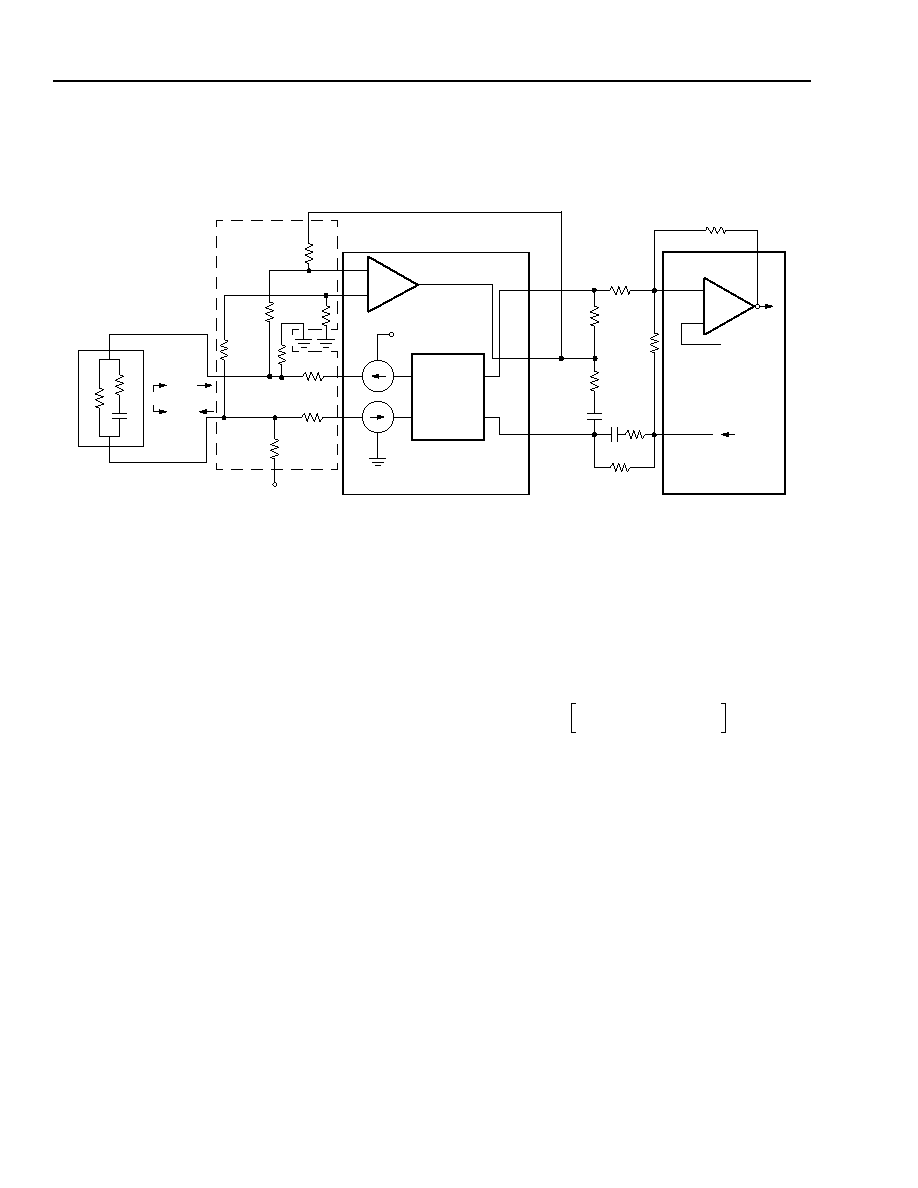
The following diagram and table show the basic com-
ponents required with the L8574 SLIC. Specific compo-
nent values are given in cases where the value is fixed.
In cases where the value may change (i.e., compo-
nents that determine the ac interface), the value is not
listed but equations to determine these values are
given later in this document.

Lucent Technologies Inc.
19
Data Sheet
October 1998
Relay, and Protector (SRP) for Long Loop and TR-57 Applications
L8574D Resistive Subscriber Line Interface Circuit (SLIC), Ring
Applications
(continued)
General
(continued)
12-3384.d (F)
* Optional components to improve PSRR by 6 dB.
Figure 5. External Components Required
R1
R2
PT
A
PRB
PRA
V
RNG
V
BA
T2
FGND
V
BA
T1
R3 100 k
R5 200 k
+5 D
V
CCA
AGND
V
DD
DGND
+5 D
0.1
µ
F
CV
DD
L8574
RCVN
XMT
PT
TS
PR
R10 600 k
RS
V
BF
RSW
C
LIM
33 nF
RTS
0.22
µ
F
C
RT
0.1
µ
F
CBN
CLIM
VF
R
O(n)
B3
B0
B2
CE
B1
PARALLEL DATA
INTERFACE TO
CONTROL LOGIC
CS
NSTAT
IRCV
RGBN
RDO
19
16
15
14
13
12
11
9
44
1
4
GS
X
(n)
1/4
T7504
VF
X
IN(n)
R
RV1
R
HB1
K1
17
18
2, 36
2, 27, 35
RINGING
SUPPLY
19.6 k
C
BIAS1
20 V
27
23,
34
22
7
8
38
40
R
BIAS2
C
BIAS2
+
V
FX
C
B1
R4
R6 200 k
R8 1 k
R7 1 k
R
RT
1 M
41
42
31
30
43
25
21
20
33
3
R
CBN3
R
CBN2
1 M
5.11 k
DG
0.1
µ
F
200
100 k
200
R
CBN1
C
CBN1
R
CBN4
301 k
9.53 k
C
CBN2
0.01
µ
F
R
BIAS1
10
µ
F
D
SPEED
0.47
µ
F
19.6 k
C
VBAT
0.1
µ
F
RESISTOR
MODULE
R9
20 k
R
RV2
R
GX
C
B2
0.1
µ
F
R
T1
V
FX
XMT
C
2
R
T2
0.1
µ
F
CV
CC
RESISTOR
MODULE
R
CX1
R
GBN
C
GBN
50 k
*
47 pF*
TIP
RING
F1
F2

20
Lucent Technologies Inc.
Data Sheet
October 1998
Relay, and Protector (SRP) for Long Loop and TR-57 Applications
L8574D Resistive Subscriber Line Interface Circuit (SLIC), Ring
Applications
(continued)
General
(continued)
Table 15. External Components Required
1. Power is continuous rms power.
2. R
1
/R
2
= 1, with a tolerance of 0.35% for 50 dB longitudinal balance, 0.2% for 58 dB longitudinal balance. Fuses F1 and F2 provide fail-safe
operation if excessive overvoltage conditions exist on Tip and Ring. They will not operate if the total power dissipation of the entire resistor
network is
5 W at 85
∞
C.
3. (R
3
+ R
6
)/(R
4
+ R
5
) = 1 with a tolerance of 0. 35% for 50 dB longitudinal balance, 0.2% for 58 dB longitudinal balance.
4. R
9
/R
1
= 100 with a tolerance of 0.5%.
Comp. Function
Implementation
Value
Attribute
1
F1
Fuse Protector
Resistor Module
--
--
F2
Fuse Protector
Resistor Module
--
--
R
1
dc Feed Protection
Resistor Module
200
1.0%, 2 W
2
R
2
dc Feed Protection
Resistor Module
200
1.0%, 2 W
2
R
3
Transmit Gain
Resistor Module
100 k
1.0%, 25 mW
3
R
4
Transmit Gain
Resistor Module
100 k
1.0%, 25 mW
3
R
5
Transmit Gain
Resistor Module
200 k
1.0%, 25 mW
3
R
6
Transmit Gain
Resistor Module
200 k
1.0%, 25 mW
3
R
7
Protection
Resistor Module
1 k
2.0%, 0.1 W
R
8
Protection
Resistor Module
1 k
2.0%, 0.1 W
R
9
Battery Noise Cancellation
Resistor Module
20 k
10 mW
4
R
10
Ringing Resistor
Module
600
1.0%, 1.6 W
(14 W for 250 ms)
C
VCC
V
CC
Filter
External
0.1
µ
F
20%, 10 V
C
VDD
V
DD
Filter
External
0.1
µ
F
20%, 10 V
C
BAT
V
BAT
Filter
External
0.1
µ
F
20%, 100 V
C
LIM
Current Limit
External
33 nF
20% 100 V
R
CBN1
Battery Noise Cancellation
External
5.11 k
1%, 1/16 W
R
CBN2
Battery Noise Cancellation
External
301 k
1%, 1/16 W
R
CBN3
Battery Noise Cancellation
External
9.53 k
1%, 1/16 W
R
CBN4
Battery Noise Cancellation
External
1 M
1%, 1/16 W
C
CBN1
Battery Noise Cancellation
External
0.22
µ
F
20%, 100 V

Lucent Technologies Inc.
21
Data Sheet
October 1998
Relay, and Protector (SRP) for Long Loop and TR-57 Applications
L8574D Resistive Subscriber Line Interface Circuit (SLIC), Ring
Applications
(continued)
General
(continued)
Table 15. External Components Required (continued)
1. Power is continuous RMS power.
2. R
1
/R
2
= 1, with a tolerance of 0.35% for 50 dB longitudinal balance, 0.2% for 58 dB longitudinal balance. Fuses F1 and F2 provide fail-safe
operation if excessive overvoltage conditions exist on Tip and Ring. They will not operate if the total power dissipation of the entire resistor
network is
5 W at 85
∞
C.
3. (R
3
+ R
6
)/(R
4
+ R
5
) = 1 with a tolerance of 0. 35% for 50 dB longitudinal balance, 0.2% for 58 dB longitudinal balance.
4. R
9
/R
1
= 100 with a tolerance of 0.5%.
5. Optional components to improve PSRR by 6 dB.
Comp.
Function
Implementation
Value
Attribute
1
C
CBN2
Battery Noise Cancellation
External
0.01
µ
F
20%, 100 V
C
GBN
5
Battery Noise Cancellation
External
47 pF
20%, 100 V
R
GBN
5
Battery Noise Cancellation
External
50 k
20%, 100 V
C
RT
Ring Trip
External
0.1
µ
F
20%, 100 V
R
RT
Ring Trip
External
1 M
1%, 1/16 W
R
BIAS1
dc Bias for On-hook Trans.
External
19.6 k
1%, 1/16 W
R
BIAS2
dc Bias for On-hook Trans.
External
19.6 k
1%, 1/16 W
C
BIAS1
ac Transmission
External
10
µ
F
20%, 100 V
C
BIAS2
ac Transmission
External
0.47
µ
F
20%, 100 V
D
SPEED
Reduce Settling Time Off-hook
to On-hook
External
20 V
Zener
C
B1
dc Blocking
External
0.1
µ
F
20%, 10 V
C
B2
dc Blocking
External
0.1
µ
F
20%, 10 V
R
T1
ac Interface
External
See ac Design Equations
1%, 1/32 W
R
T2
ac Interface
External
See ac Design Equations
1%, 1/32 W
R
GX
ac Interface
External
See ac Design Equations
1%, 1/32 W
R
GX1
ac Interface
External
See ac Design Equations
1%, 1/32 W
R
RV1
ac Interface
External
See ac Design Equations
1%, 1/32 W
R
RV2
ac Interface
External
See ac Design Equations
1%, 1/32 W
C
2
ac Interface
External
See ac Design Equations
1%, 1/32 W
R
HB1
ac Interface
External
See ac Design Equations
1%, 1/32 W

22
Lucent Technologies Inc.
Data Sheet
October 1998
Relay, and Protector (SRP) for Long Loop and TR-57 Applications
L8574D Resistive Subscriber Line Interface Circuit (SLIC), Ring
Applications
(continued)
Resistor Module
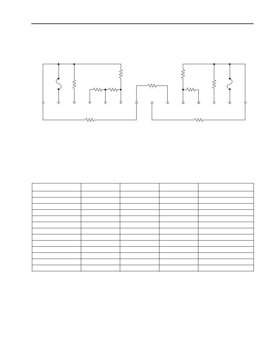
The L8574 requires certain external resistors at the Tip and Ring interface. Because of matching and protection
requirements, one of the most economical options recommended to implement these resistors is in a thick-film
resistor module. A schematic and a brief description of the function of each of these resistors is given in Figure 6.
Note that Microelectronic Modules Corporation
MMC* A31A8574AA and MMC A11A8574AA thick-film resistor
modules are application-specific resistor modules designed for use with the L8574 SLIC. The values, tolerance,
matching, and power rating of the
MMC A31A8574AA and MMC A11A8574AA modules are given in Table 16.
Resistors R
1
and R
2
are the dc feed resistors. R1 is connected from battery to Ring and R
2
is connected from Tip to
ground. The dc loop current is fed to the subscriber loop via these resistors. The resistors set the dc feed resis-
tance, which is R
1
+ R
2
(400 = 200 + 200).
Resistors R
1
and R
2
also provide a common-mode impedance of (200
||
200) 100
. These resistors will primarily
determine the longitudinal balance of the line circuit; thus, they must be matched appropriately to meet longitudinal
balance requirements (0.35% for 50 dB and 0.2% for 58 dB). Also, they have a significant impact on the termination
impedance of the SLIC. Feedback using external components (external components when a first- or second-gener-
ation codec is used) allows the user to set the termination impedance at 600
, or most ITU-T recommended ter-
mination impedances.
Under normal operating conditions, the current through resistors R
1
and R
2
is limited by the current-limit circuitry to
25 mA. Thus, the 2 W rating of resistors R
1
and R
2
in
MMC A31A8574AA and MMC A11A8574AA is adequate for
normal operation. The power rating of these resistors is discussed more in the Protection section of this data sheet.
*
MMC is a registered trademark of Microelectronic Modules Corporation. For additional information, contact Microelectronic Modules Corpo-
ration (MMC), 2601 S. Moorland Rd., New Berlin, WI 53151 U.S.A.: Tel. 414-785-6506, FAX 414-785-6516, e-mail sales@mmccorp.com.

Lucent Technologies Inc.
23
Data Sheet
October 1998
Relay, and Protector (SRP) for Long Loop and TR-57 Applications
L8574D Resistive Subscriber Line Interface Circuit (SLIC), Ring
Applications
(continued)
Resistor Module
(continued)
5-5279 (F)
Notes:
1. Pin numbers and resistor labels are per
MMC A31A8574AA and MMC A11A8574AA descriptions.
2. Node labels are per L8574 package.
3. For 600 V power cross, resistor networks should "open" in less than 40 ms.
Figure 6. Resistor Network
Table 16.
MMC A31A8574AA and MMC A11A8574AA Module
1. Continuous (RMS) power.
2. For 50 dB longitudinal balance; 0.2% for 58 dB balance.
Note: Fuses F1 and F2 provide fail-safe operation if excessive overvoltage conditions exist on Tip and Ring. They will not operate if the total
power dissipation of the entire resistor network is
5.0 W @ 85
∞
C.
Resistor
Value
Tolerance
Power
1
Surge Rating
R
1
200
1.0%
2.0 W
Lightning: Power Cross
R
2
200
1.0%
2.0 W
Lightning: Power Cross
R
3
100 k
1.0%
25 mW
None
R
4
100 k
1.0%
25 mW
None
R
5
200 k
1.0%
25 mW
Lightning: Power Cross
R
6
200 k
1.0%
25 mW
Lightning: Power Cross
R
7
1 k
2.0%
0.1 W
Lightning: Power Cross
R
8
1 k
2.0%
0.1 W
Lightning: Power Cross
R
9
20 k
--
10 mW
None
R
10
600
1.0%
1.6 W
14 W for 250 ms
R
9
/R
1
100
0.5%
--
--
R
1
/R
2
1
0.35%
2
--
--
(R
3
+ R
6
)/(R
4
+ R
5
)
1
0.35%
2
--
--
1
RING
PR
RGBN
GND
RS
V
BF
GND
RSW
TS
XMT
PT
TIP
F2
R
7
2
3
4
5
R
9
R
3
7
6
R
5
R
10
R
6
R
4
12
11
10
9
8
13
14
F1
R
8
R
2
R
1

24
24
Lucent Technologies Inc.
Data Sheet
October 1998
Relay, and Protector (SRP) for Long Loop and TR-57 Applications
L8574D Resistive Subscriber Line Interface Circuit (SLIC), Ring
Applications
(continued)
Resistor Module
(continued)
Resistors R
3
--R
6
set the gain of the SLIC in the
transmit (2-wire to 4-wire) direction. This is shown in
Figure 7.
5-5277 (F)
Figure 7. L8574 SLIC Matching Requirements
The matching of resistors R
3
--R
6
will determine the
gain accuracy of the SLIC; therefore, these resistors
must be matched accordingly. Their matching require-
ments are given in Table 16.
Because of the high resistance values, the normal
operating power of resistors R
3
--R
6
will be relatively
low. Given design margin and thick-film technology
capabilities, a power rating of 250 mW for these resis-
tors is not unreasonable.
Resistors R
7
and R
8
are used to couple the PT and PR
current drive amplifiers to Tip and Ring. Since PT and
PR drive amplifiers are current sources, the value of
the series resistance does not affect the loop length or
other performance of the SLIC, and may be arbitrarily
high for protection purposes. A value of 1 k
is ade-
quate for protection purposes.
Under normal operating conditions, these resistors will
see the battery voltage less the Tip/Ring voltage.
Assuming a Tip/Ring voltage of 6 V (representative of a
short into a handset), the normal continuous operating
power of R
7
and R
8
is given by:
(48 V ≠ 6 V) E2/2.0 k
= 0.882 W per R
7
and R
8
resis-
tor pair
882 mW/2 = 441 mW per resistor (R
7
and R
8
)
Hence, the operating power rating of 500 mW for R
7
and R
8
. This is the normal rating for R
7
and R
8
under
normal operating conditions. The ability of these resis-
tors to withstand fault conditions depends on the power
rating.
Resistor R
9
is also included on the thick-film resistor
module. This resistor is used to set the gain of the bat-
tery noise cancellation circuit. See the Battery Noise
Cancellation section of this data sheet for design equa-
tions to set the value of R
9
.
Power ringing is applied to the line circuit through resis-
tor R
10
. One side of R
10
is connected to L8574 node
RSW. RSW is the output of the integrated solid-state
ringing access switch, SW3. The other side of R
10
is
connected to the 200
Ring feed resistor, R
1
. Resistor
R
10
also serves as a current-limiting resistor. Fault cur-
rent through the solid-state ringing access switch,
SW3, is limited by R
10
. SW3 is rated for 2 A maximum
for a 10
µ
s x 1000
µ
s (lightning) pulse. Continuous cur-
rent through this switch should be less than 150 mA.
R
10
in resistor modules
MMC A31A8574AA and MMC
A11A8574AA is chosen to be 600
.
Protection
Because of the resistive feed architecture, a simple
inexpensive protection scheme that does not require
an external protection device may be used. The
MMC
A31A8574 resistor module has specifications which
are qualified to ITU-T K20,
UL* 1459, UL 497A, FCC
Part 68.302 (d) & (e), and REA Form 397G specifica-
tion. The
MMC A11A8574AA resistor module, in addi-
tion to meeting all the specifications of the
MMC
A31A8574, also meets Bellcore 1089 requirements.
Lightning and power-cross protection are provided
by the two external dc feed (and current-limiting) resis-
tors, R
1
and R
2
, in the external resistor module. Under
fault conditions, these resistors serve as fault current-
limiting resistors. These resistors are designed to sur-
vive lightning surges. They are also designed to contin-
uously dissipate 4 W each and to survive 1 Arms @
60 Hz power crosses of
1 second in duration. Sus-
tained power dissipation above these levels will cause
degradation and eventual failure; however, the resistors
are designed to fail gracefully under these conditions.
Pins PT and PR are isolated from the loop by external
1000
resistors, and pin V
BF
is isolated from the loop
by the Ring-side, 200
dc feed resistor. These pins
must have adequate fault protection which operates
outside of their normal operating voltages. All three
pins are protected by SCRs which clamp the surge
currents (both positive and negative) to FGND. The
TIP
RING
R
5
200 k
R
6
200 k
R
4
100 k
≠
+
XMT
R
3
100 k
*
UL is a registered trademark of Underwriters Laboratories, Inc.

Lucent Technologies Inc.
25
Data Sheet
October 1998
Relay, and Protector (SRP) for Long Loop and TR-57 Applications
L8574D Resistive Subscriber Line Interface Circuit (SLIC), Ring
Applications
(continued)
Protection
(continued)
sense inputs, TS and RS, are protected with diodes to
battery (V
BAT1
) and V
CCA
and the series high-value
external resistors which connect them to Tip and Ring.
Because the battery noise cancellation input CBN is
connected to pin V
BF
through a 0.1
µ
F capacitor, it must
also be protected. Internally, it is protected with an 8 V
zener diode connected to V
CCA
. An external resistor of
at least 3 kW (5 kW is recommended) is required to
limit the surge current. No external protection device is
required.
Tip/Ring Drivers
The L8574 has two Tip/Ring drivers with outputs called
PT and PR. Each driver operates as a current source
capable of sinking or sourcing adequate ac signal cur-
rent plus the dc bias current that is required during on-
hook transmission.
Receive Interface
The receive interface circuitry couples the differential
signal on receive inputs IRCV and RCVN to the Tip/
Ring drivers. Input IRCV is a low-impedance (<5
)
current input while RCVN is a high-impedance voltage
input. Internal feedback forces the voltage at IRCV to
be equal to RCVN so that a voltage applied to RCVN
causes a current flow out of IRCV which equals that
voltage divided by the impedance connected from
IRCV to AGND (assuming the input voltage is refer-
enced to AGND).
The receive interface and Tip/Ring drivers provide a
current gain of 200; i.e., a differential output current
flows from PT to PR which is 200 times the current
flowing into IRCV. The receive interface also provides a
level shift since the inputs, IRCV and RCVN, are refer-
enced to analog ground, while the outputs, PT and PR,
swing between V
CCA
and V
BAT1
. The receive interface
ensures that the input current is not converted to a
common-mode current at PT and PR.
Transmit Interface
The transmit interface circuitry interfaces the differen-
tial voltage on Tip and Ring to transmit output XMT. The
Tip/Ring differential voltage (both ac and dc) appears
on output XMT with a gain of 0.5. The transmit interface
uses an operational amplifier with four external resis-
tors to perform a differential to single-ended conver-
sion. The operational amplifier inputs are TS and RS.
Output XMT is referenced to ground (AGND). The lon-
gitudinal balance and gain accuracy at XMT depends
on the matching of the external resistors (0.35%).
Because a large dc potential exists at XMT, a capacitor
must be used to couple the ac signal to the low-voltage
codec circuitry.
Battery Noise Cancellation
The battery noise cancellation circuit senses the ac
noise on the battery via the capacitor connected from
input CBN to V
BF
. It couples this noise, 180
∞
out of
phase, to the Ring current drive amplifier. This cancels
the battery noise that is coupled to the Ring through
the feed resistor connected to V
BF
.
Additionally, it ensures longitudinal balance, which
depends only on the matching of the battery feed resis-
tors by creating an ac ground at V
BF
with respect to sig-
nals on the Ring lead.
For the cancellation to operate properly, both the phase
and gain must be accurate. The battery noise cancella-
tion gain is a transconductance which is equal to 100
divided by the resistor connected from RGBN to
ground (AGND). This value must be equal to the recip-
rocal of the dc feed resistor (1/200). That is:
100/R
9
= 1/200
R
9
= 20 k
It is advantageous if resistors R
9
and R
1
are matched
and tracked thermally, i.e., located on the same film
integrated circuit (FIC).
PSRR can be improved by adding a 47 pF capacitor in
series with a 50 k
resistor from R
GBN
to ground.
Also, to implement the battery noise cancellation func-
tion, connect the following circuit from CBN to V
BF
and
analog ground.
5-5278a (F)
Figure 8. Implementing the Noise Cancellation
Function
V
BF
CBN
301 k
0.1
µ
F
5.11 k
0.01
µ
F
L8574

26
26
Lucent Technologies Inc.
Data Sheet
October 1998
Relay, and Protector (SRP) for Long Loop and TR-57 Applications
L8574D Resistive Subscriber Line Interface Circuit (SLIC), Ring
Applications
(continued)
On-Hook Transmission
During the on-hook transmission and talk/on-hook
transmission states, the L8574 provides 750
µ
A dc bias
current out of the Tip/Ring current driver amplifiers.
This creates a dc voltage drop across the external 19.6
k
resistors, R
BIAS1
and R
BIAS2
, which provides suffi-
cient dc bias to support on-hook transmission. The
switchhook detector is adjusted to compensate for this
dc bias current. The L8574 is able to support on-hook
transmission to drive a 3.17 dBm signal into a 600
or
900
ac loop. The capacitors, C
BIAS1
and C
BIAS2
, pro-
vide an ac path so transmission is not distorted by
R
BIAS1
and R
BIAS2
. Zener diode, D
SPEED
, reduces the
settling time transition from on- to off-hook.
Parallel Data Interface
A 6-wire parallel interface (CE, CS, B0, B1, B2, and B3)
is used to pass control information from the control
logic on the line card to the L8574. The L8574 has
eight operating states. These states are selected using
three logic input bits, B0--B2, according to the truth
table shown in Table 14. Logic input B3 operates a
relay driver independent of the state of bits B0--B2.
Data on the parallel data bus, B0--B3, is loaded into a
4-bit latch on the L8574 on the low-to-high transition of
the channel select lead CS. Changes in the data at
inputs B0--B3 do not affect the L8574 while CS is
either low or high. A low on channel enable lead CE
asynchronously resets the 4-bit latch to 1111 (scan
state with the relay driver off) and disables the channel
select lead CS (i.e., CS is prevented from loading any
data into the 4-bit latch). A high on CE enables CS.
State transitions and delays between transitions are left
to the discretion of the user since, except for fault con-
ditions, the state of the L8574 depends only on the
external control provided through the logic interface.
Supervision
The L8574 offers the ring trip, loop closure, and ther-
mal shutdown functions. The status of these functions
are provided as device outputs. The outputs of the ring
trip and off-hook supervision detectors are multiplexed
into a single output called NSTAT. The device state
determines which output is connected to NSTAT. The
device state table, Table 14, details which supervision
output (loop closure or ring trip) is seen at NSTAT dur-
ing a given device state.
Detector values are independent of office battery and
are valid over the entire range of V
BAT1
and V
BAT2
. How-
ever, NSTAT must indicate an on-hook (NSTAT = 1) if
either V
BAT1
or V
BAT2
is disconnected (open circuit) from
its dc source and an off-hook (NSTAT = 0) if the L8574
is in thermal shutdown. V
BAT1
and V
BAT2
are defined as
disconnected depending on the voltage at the power
supply pins as follows (the pins of supplies which have
more than one pin are shorted together):
If V
BAT1
≠20 V (i.e., more negative than ≠20 V) and
V
BAT2
≠20 V, then NSTAT must operate normally.
If V
BAT1
≠10 V (i.e., more positive than ≠10 V) or V
BAT2
≠10 V, then NSTAT must be on-hook (NSTAT = 1).
The status of the thermal shutdown circuit is output on
B3 when CS is high (thermal shutdown = 0 V).
Off-Hook Detection
The off-hook or loop closure threshold on the L8574
SLIC is internally fixed. Off-hook is indicated (NSTAT =
0) if the loop resistance is a maximum 2700
. On-
hook is indicated (NSTAT = 1) if the loop resistance is a
minimum 4400
.
Ring Trip
The ring trip threshold is set by resistor R
10
in the resis-
tor module. With R
10
set to 600
, the circuit is guaran-
teed to ring trip up to 1840
. With a 20 Hz ringing
source, the trip time is guaranteed less than 200 ms.
The ring trip circuit assumes uses of battery-backed
ringing. Pretrip immunity is such that a load across
Tip and Ring of 10 k
in parallel with an 8
µ
F capacitor
will not cause ring trip. Three external components
are required for ring trip, a 1 M
resistor from R
TS
to
V
BF
, resistor R
10
, which is a 600
resistor from R
SW
to V
BF
, and a 0.1
µ
F capacitor from R
SW
to R
TS
. The
components required for ring trip circuit are shown in
Figure 9. Note that R
10
is implemented in the resistor
module. All other components are discrete.
5-5276 (F)
Figure 9. Ring Trip Threshold
600
R
10
1 M
RTS
RSW
V
BF
0.1
µ
F
L8574

Lucent Technologies Inc.
27
Data Sheet
October 1998
Relay, and Protector (SRP) for Long Loop and TR-57 Applications
L8574D Resistive Subscriber Line Interface Circuit (SLIC), Ring
Applications
(continued)
Thermal Shutdown
If the silicon temperature rises above a nominal 145
∞
C,
the L8574 will enter a thermal shutdown mode where
all switches are off and the SLIC is in a state that is
functionally equivalent to the disconnect state.
Relay Driver
The L8574 offers a single integrated relay driver. The
relay driver output RDO is low (relay operated) when a
low input on B3 is latched into the device. The driver
has sufficient driver capability to provide 70 mA with a
1.0 V drop and 20 mA with a 0.4 V drop. Turn-off and
turn-on times are a maximum of 10
µ
s.
Solid-State Ringing Access
The L8574 offers a solid-state ringing access switch for
power ringing access and for the associated line break
function. During the Ringing state, unbalanced battery-
backed power ringing is applied to the Ring lead
through resistors R
10
and R
1
via ringing access switch
SW3. The Ring drive amplifier of the L8574 SLIC is iso-
lated from the subscriber loop via the integrated line
break switch SW2 during the power ringing state. Since
the Tip lead of the L8574 SLIC is tied to ground via
resistor R
2
, no line break function is associated with the
Tip lead. The return ground path for the power ringing
signal is via R
2
.
The line break switch, SW2, is implemented using a
high-voltage MOS transistor. This gives a linear V-I
characteristic, as seen in Figure 3. The ON resistance
of this switch is a nominal 50
with a maximum 100
.
This switch is current limited to a nominal 35 mA and
has a maximum off-state voltage rating of 320 V. The
ringing access switch, SW3, is implemented using a
pnpn type structure. This gives a linear V-I characteris-
tic with an offset through the origin, as shown in Figure
4. This offset is less than 3 V. The off-state voltage rat-
ing is 500 V. Surge current (10
µ
s x 1000
µ
s) through
this switch must be limited to less than 2 A. Steady
state current through this switch must be limited to less
than 150 mA.
Battery Supplies
There are two battery pins on the L8574, V
BAT1
and
V
BAT2
. These two nodes may be connected to a com-
mon negative battery voltage. The magnitude of the
battery should be sufficient to supply the required dc
current into the specified (long) loop requirement.
Integrated into the L8574 is solid-state switch, SW1.
SW1 has similar characteristics to the line break
switch, SW2, including the 35 mA current limit. When
SW1 is closed, the battery is applied through SW1 from
the V
BAT1
node. dc current from the battery will be lim-
ited by the current-limiting action of SW1. When SW1 is
open, the battery at V
BAT1
is isolated from the loop. The
internal current-limit circuit is associated with the V
BAT2
node; thus, when the current-limit circuit is active, the
battery is applied to the subscriber loop through V
BAT2
node and through the internal current-limiting circuitry,
limiting dc current to the subscriber loop to 28 mA.
When the current-limit circuit is not active, the voltage
battery at V
BAT2
is isolated from the loop.
The state of SW1 and the current-limiting circuit is con-
trolled via logic inputs B0--B2. The L8574 state table
(Table 14) details, for a given operational state, the con-
dition of SW1 and the current-limit circuit.
dc Characteristics
V-I Characteristics
Resistors R
1
and R
2
are the dc feed resistors. R
1
is
connected from battery to Ring, and R
2
is connected
from Tip to Ground. The dc loop current is fed to the
subscriber loop via these resistors. When the L8574 is
operating in the linear region of the V-I characteristic,
the dc feed resistance or slope of this region of opera-
tion is determined by the sum of resistors R
1
plus R
2
.
The slope of the V-I characteristic will be ≠1/400
.
When the L8574 is operating in the current-limited
region of the V-I characteristic, the current will be con-
stant, regardless of loop length, and will be set and
fixed by the internal current-limit circuit. The current
limit is internally fixed to a nominal 28 mA. Connect a
33 nF capacitor from C
LIM
to V
BF
. Note that there is a
slope of 1/10 k
to the V-I characteristic in the current-
limited region of operation.

28
28
Lucent Technologies Inc.
Data Sheet
October 1998
Relay, and Protector (SRP) for Long Loop and TR-57 Applications
L8574D Resistive Subscriber Line Interface Circuit (SLIC), Ring
dc Characteristics
(continued)
V-I Characteristics
(continued)
In longer loops, the L8574 will operate in the linear
region of operation, and in short loops, to conserve
power, the L8574 will operate in the (fixed) current-limit
region of operation. A typical V-I characteristic for the
L8574 is shown in Figure 10 below.
12-3050.e (C)
Note: V
BAT1
= ≠48 V, V
BAT2
= ≠48 V; I
LIM
= 28 mA; R
DC
= 400
.
Figure 10. Loop Current vs. Loop Voltage
Loop Length
The loop range is calculated as follows:
R
L
= ({
|
V
BAT
|
≠ V
OHLIM
}/I
LIMIT
) ≠ R
1
≠ R
2
Where:
R
L
is the dc resistance of the subscriber loop.
V
OHLIM
is the overhead or drop associated with the cur-
rent-limit circuit, typically 2.2 V.
I
LIMIT
is the minimum specified current that is required
at the maximum loop length, typically 18 mA.
|
V
BAT
|
is the minimum magnitude of the battery--
assume 43.2 V.
R
1
= R
2
= dc feed resistors = 200
.
R
L
= ({43.2 V ≠ 2.2 V}/0.018 A) ≠ 200
≠ 200
=
1877
.
ac Design
Codec Features and Selection Summary
There are four key ac design parameters:
s
Termination impedance is the impedance looking
into the 2-wire port of the line card. It is set to match
the impedance of the telephone loop in order to mini-
mize echo return to the telephone set.
s
Transmit gain is measured from the 2-wire port to
the PCM highway.
s
Receive gain is done from the PCM highway to the
transmit port.
s
Hybrid balance
network cancels the unwanted
amount of the receive signal that appears at the
transmit port.
At this point in the design, the codec needs to be select-
ed. The discrete network between the SLIC and the co-
dec can then be designed. Below is a brief codec
feature and selection summary.
First-Generation Codecs
These perform the basic filtering, A/D (transmit), D/A
(receive), and
µ
-law/A-law companding. They all have
an op amp in front of the A/D converter for transmit
gain setting and hybrid balance (cancellation at the
summing node). Depending on the type, some have
differential analog input stages, differential analog out-
put stages, and
µ
-law/A-law selectability. This genera-
tion of codec has the lowest cost. It is most suitable for
applications with fixed gains, termination impedance,
and hybrid balance.
Second-Generation Codecs
This class of devices includes a microprocessor inter-
face for software control of the gains and hybrid bal-
ance. The hybrid balance is included in the device. ac
programmability adds application flexibility and saves
several passive components. It also adds several I/O
latches that are needed in the application. It does not
have the transmit op amp, since the transmit gain and
hybrid balance are set internally.
LOOP CURRENT (mA)
0
10
20
50
0
20
30
40
50
LOOP VOLTAGE (V)
30
40
10
1
10 k
I
LIM
≠1
R
DC1
≠1
400
=

Lucent Technologies Inc.
29
Data Sheet
October 1998
Relay, and Protector (SRP) for Long Loop and TR-57 Applications
L8574D Resistive Subscriber Line Interface Circuit (SLIC), Ring
ac Design
(continued)
Codec Features and Selection Summary
(continued)
Third-Generation Codecs
This class of devices includes the gains, termination im-
pedance, and hybrid balance--all under microproces-
sor control. Depending on the device, it may or may not
include latches.
In the codec selection, increasing software control and
flexibility are traded for device cost. To help decide, it
may be useful to consider the following:
s
Will the application require only one value for each
gain and impedance?
s
Will the board be used in different countries with dif-
ferent requirements?
s
Will several versions of the board be built? If so, will
one version of the board be most of the production
volume?
s
Does the application need only real termination
impedance?
s
Does the hybrid balance need to be adjusted in the
field?
Design Equations
The following section gives the relevant design equa-
tions to choose component values for any desired gain,
termination, and balance network, assuming a complex
termination is desired. Complex termination will be
specified in one of the two forms shown below.
12-3425(F)
Figure 11. Equivalent Complex Terminations
Both forms are equivalent to each other, and it does not
matter which form is specified. The component values
in the interface circuit of Figure 11 are calculated
assuming the parallel form is specified. If the termina-
tion impedance to be synthesized is specified in the
series form, convert it to the parallel form using the
equations below:
Note that if the termination impedance is specified as
pure resistive:
Define the gain constant, K, as follows:
Where,
R
X
= desired receive (or PCM to Tip/Ring)
gain in dB
T
X
= desired transmit (or Tip/Ring to PCM)
gain in dB
Where |Z
T
| (1 kHz) is the magnitude of the complex ter-
mination impedance Z
T
being synthesized. This equa-
tion assumes that the TLP of the codec is 0 dBm
referenced to 600
.
The following equation applies when referring to
Figure 11:
Where,
= 2
= 1000 Hz
CR
1
R
2
is defined per Figure 11 (series form), and
R
1
R
2
C
R
2
¥
R
1
¥
C¥
(SERIES FORM)
(PARALLEL FORM)
R
1
R
1
R
2
+
=
R
2
R
1
2
R
2
R
1
+
R
2
-------------------------------
=
C
C
1
2
R
1
R
2
-------
R
1
R
2
-------
2
+
+
-------------------------------------------
=
R
2
R
2
0 and C = C
=
=
=
K
RCV
K
0
10
Rx/20
for receive gain
=
K
TX
1
K
0
------
10
Tx/20
for transmit gain
=
K
0
Z
T
1
kHz
600
--------------------------
=
= power transfer ratio
Z
T
2
C
2
R
1
R
2
2
R
1
R
2
j
R
2
2
C
≠
+
+
1
2
R
2
2
C
2
+
---------------------------------------------------------------------------------------
=
Z
T
2
C
2
R
1
R
2
2
R
1
R
2
+
+
1
2
R
2
2
C
2
+
-----------------------------------------------------------
2
R
2
2
C
1
2
R
2
2
C
2
+
-----------------------------------
2
+
=

30
Lucent Technologies Inc.
Data Sheet
October 1998
Relay, and Protector (SRP) for Long Loop and TR-57 Applications
L8574D Resistive Subscriber Line Interface Circuit (SLIC), Ring
ac Design
(continued)
Design Equations
(continued)
12-3429.b (F).r3
Figure 12. Initial ac Interface for Complex Termination Between L8574 SLIC and T7504 Codec
Note: dc Blocking Capacitor (C
B
) Not Shown, C
T
and C
R
Separate
V
RN
RECEIVE
INTERFACE
+
≠
R
T2
R
RV2
R
HB1
R
GX
GSX
VFXIN
VFRO
1/4 T7504 CODEC
Z
T/R
+
≠
V
T/R
I
T/R
+2.4 V
C
R
1/2 L8574
R
GX1
R
RV1
C
T
R
T1
Z
IRP
≠
+
AX
V
XMT
L
RP
V
RN
XMT
I
RP
PT
PR
V
BAT
TS
RS
V
BAT
R
1
R
2
C
1
RESISTOR
MODULE
200 k
200 k
100 k
200
200
100 k
1 k
1 k
The Tip/Ring differential current is given by:
The voltage at pin XMT is given by:
The component values in the ac interface of Figure 12
are calculated (for the transmit and receive gains
defined by the respective gain constants K
RX
and K
RCV
,
and for the termination impedance seen in Figure 11)
using the following equations:
Note that the 200
feed resistors contribute 400
to
the termination impedance. The termination impedance
associated with the circuit in Figure 12 consists of this
inherent 400
feeding impedance in parallel with:
s
A negative impedance, where,
s
A positive impedance, where,
The negative and positive impedance terms are used
to adjust the termination impedance from the inherent
400
to any complex termination.
I
T/R
200 I
RP
V
RN
Z
IRP
-----------
≠
=
V
XMT
V
T/R
≠
2
--------------
=
R
RV1
100R
1
K
RCV
-------------------
=
R
RV2
100R
2
K
RCV
-------------------
=
C
R
K
RCV
C
100
--------------------
=
R
GX1
R
GX1
R
T1
+
------------------------------
R
RV1
100
-------------
1
600
----------
1
R
1
--------
≠
=
400
= 2 x 200
feed resistors
R
GX
2
x
K
TX
R
GX1
R
T1
+
(
)
=
C
T
C
100
---------- 1
R
GX1
R
T1
------------- 1
100R
1
R
RV1
-------------------
+
+
=
R
T2
R
2
C
C
T
---------------
=
2
100
----------
x
R
GX1
R
GX1
R
T1
+
------------------------------
R
T2
1
j
C
T
--------------
+
∑
R
GX1
R
T1
+
R
T1
------------------------------

Data Sheet
October 1998
Lucent Technologies Inc.
31
Relay, and Protector (SRP) for Long Loop and TR-57 Applications
L8574D Resistive Subscriber Line Interface Circuit (SLIC), Ring
ac Design
(continued)
Design Equations
(continued)
Using the circuit of Figure 12, the ratio of capacitors C
T
and C
R
will affect the (transmit and receive) gain flatness,
and to a lesser degree the return loss of the line circuit. Thus, depending on the requirements, C
T
and C
R
may need
to be tight tolerance capacitors.
If this is the case, capacitors C
T
and C
R
may be combined into a single capacitor with a looser tolerance. This is
illustrated in Figure 13.
12-3426.a(F).r3
Figure 13. Revised ac Interface C
T
and C
R
Combined into a Single Capacitor C
S
XMT
R
T2
C
T
IRP
C
R
V
F
R
O
R
RV2
XMT
R
T2
IRP
C
S
= C
T
+ C
R
V
F
R
O
R
RV2
R
RV1
R
RV1
--
--
--
To scale C
S
(higher), increase C
T
(and decrease R
T2
)
by increasing the R
GX1
/(R
GX1
+ R
T1
) ratio by rearrang-
ing the circuit in Figure 13 and by adding resistor R
SC
from XMT to IRP as shown below.
12-3427.abF)
Figure 14. Addition of Resistor R
SC
from XMT to IRP
Then,
Once the gains and complex termination are set, if the
hybrid balance network is identical to the termination
impedance, then the hybrid balance is set by a single
resistor (shown in Figure 12) and is computed as fol-
lows:
The L8574 SLIC is ground referenced. However, a +5 V
only codec, such as T7504, is referenced to +2.5 V. The
L8574 SLIC has sufficient dynamic range to accommo-
date an ac signal from the codec that is referenced to
+2.5 V without clipping distortion. Furthermore, a dc
current will flow between the L8574 SLIC and +5 V only
codec. With the L8574 SLIC, this current will not affect
ac performance, but it does waste power. To avoid
wasted power consumption, blocking capacitors can be
added. Capacitors should be placed to block any path
from any low impedance +2.5 V biased node on the
T7504 codec (or other +5 V only codec) to the SLIC. A
blocking capacitor (C
B
) has been added in the applica-
tion drawing in Figure 14.
After the blocking capacitor C
B
is added, the above
component values may have to be adjusted slightly to
optimize performance.
The effects of the blocking capacitor are best evaluated
and optimized by circuit simulation. Contact your
Lucent Technologies Microelectronics Group Account
Manager for information on availability of a
PSPICE*
model.
*
PSPICE is a registered trademark of MicroSim Corporation.
R
T1
R
SC
IRP
C
T
R
T2
XMT
VRN
R
GX1
C
B
VF
X
IN
R
GX1
R
GX1
R
T1
+
------------------------------
R
RV1
R
SC
||
(
)
100
-------------------------------------
1
400
----------
1
R
1
---------
≠
R
RV1
R
RV1
R
SC
+
------------------------------
+
=
R
HB
R
GX
K
TX
K
RCV
◊
-----------------------------
=

32
32
Lucent Technologies Inc.
Data Sheet
October 1998
Relay, and Protector (SRP) for Long Loop and TR-57 Applications
L8574D Resistive Subscriber Line Interface Circuit (SLIC), Ring
ac Design
(continued)
Design Equations
(continued)
As a practical design example, design the interface for
the following set of requirements:
RX = 0 dB
TX = 0 dB
ZT = 900
Hy = 900
First, calculate the gain constants:
Ko =
= 1.2247
K
RCV
= K
O
10
RX/20
= 1.2247 x 10
0/20
= 1.2247
K
TX
=
10
TX/20
= 0.8165
Second, calculate individual components:
R
RV1
= 73,487
Choose a standard value component:
R
RV1
= 73.2 k
R
RV2
=
= 0
C
R
=
=
Choose R
GX1
= 100 k
:
R
T1
= 0
C
T
=
C
T
=
R
T2
=
= 0
R
GX
= 2 x K
TX
(R
GX1
+ R
T1
)
R
GX
= 2 x 0.8165 (100 k
+ 0)
R
GX
= 163.3 k
Choose a standard value resistor:
R
GX
= 165 k
R
HB
=
R
HB
=
Therefore, for this design example, use the following
values in the circuit shown in Figure 12.
R
T1
= 0 k
R
T2
= 0
R
GX
= 165 k
R
GX1
= 100 k
R
RV1
= 73.2 k
R
RV2
= 0
R
HB1
= 165 k
C
T
=
C
R
=
Figure 15 is the application circuit with the above
values.
Z
T
600
-----------
900
600
-----------
=
1
Ko
--------
100 R
X
R
RCV
-----------------------
K
RCV
C
100
----------------------
R
GX1
R
GX1
R
T1
+
--------------------------------
R
RV1
100
--------------
1
400
-----------
1
R
1
---------
≠
=
100 k
100 k
R
T1
+
---------------------------------------
73.2 k
100
-----------------------
1
400
-----------
1
900
-----------
≠
=
100 k
100 k
R
T1
+
---------------------------------------
1.01
=
C
100
-----------
1
R
GX1
R
T1
---------------
+
1
100 R
1
R
RV1
-----------------------
+
R
2
C
C
T
----------------
R
GX
K
TX
K
RCV
◊
-----------------------------
165
k
0.8165
1.2247
◊
------------------------------------------
165 k
=

Lucent Technologies Inc.
33
Data Sheet
October 1998
Relay, and Protector (SRP) for Long Loop and TR-57 Applications
L8574D Resistive Subscriber Line Interface Circuit (SLIC), Ring
Application Diagram
12-3384.c (F)
Figure 15. TR-57 Application Diagram
200
200
PT
A
PRB
PRA
V
RNG
V
BA
T2
FGND
V
BA
T1
100 k
200 k
+5 D
V
CCA
AGND
V
DD
DGND
+5 D
0.1
µ
F
0.1
µ
F
L8574C
SLIC
RCVN
XMT
TIP
RING
PT
TS
PR
600
RS
V
BF
RSW
33 nF
RTS
0.22
µ
F
0.1
µ
F
0.01
µ
F
CBN
CLIM
165 k
VF
R
O(n)
B3
B0
B2
CE
B1
PARALLEL DATA
INTERFACE TO
CONTROL LOGIC
CS
NSTAT
IRCV
RGBN
RDO
19
16
15
14
13
12
11
9
44
1
4
GS
X
(n)
1/4
T7504
VF
X
IN(n)
100 k
73.2 k
20 k
165 k
K1
17
18
2, 36
2, 27, 35
RINGING
SUPPLY
19.6 k
10
µ
F
20 V
27
23,
34
22
7
8
38
40
19.6 k
0.47
µ
F
+
V
FX
0.1
µ
F
100 k
200 k
1 k
1 k
1 M
41
42
31
30
43
25
21
20
33
3
9.53 k
301 k
1 M
5.11 k
DG
V
FX
D
SPEED
F1
F2
RESISTOR
NETWORK
RESISTOR
NETWORK
C
VBAT
0.1
µ
F

34
Lucent Technologies Inc.
Data Sheet
October 1998
Relay, and Protector (SRP) for Long Loop and TR-57 Applications
L8574D Resistive Subscriber Line Interface Circuit (SLIC), Ring
Outline Diagram
44-Pin PLCC
Dimensions are in millimeters.
5-2506 (C) r07
4.57
MAX
1.27 TYP
0.53
MAX
0.10
SEATING PLANE
0.51 MIN
TYP
1
6
40
7
17
29
39
18
28
PIN #1 IDENTIFIER
ZONE
16.66 MAX
17.65 MAX
16.66
MAX
17.65
MAX

Lucent Technologies Inc.
35
Data Sheet
October 1998
Relay, and Protector (SRP) for Long Loop and TR-57 Applications
L8574D Resistive Subscriber Line Interface Circuit (SLIC), Ring
Ordering Information
Device Part No.
Description
Package
Comcode
LUCL8574DP-D
Resistive SLIC, Ring Relay, and Protector
for Long Loop and TR-57 Applications
44-Pin PLCC
(Dry-bagged)
107874794
LUCL8574DP-DT
Resistive SLIC, Ring Relay, and Protector
for Long Loop and TR-57 Applications
44-Pin PLCC
(Tape and Reel, Dry-bagged)
107840688

Lucent Technologies Inc. reserves the right to make changes to the product(s) or information contained herein without notice. No liability is assumed as a result of their use or application. No
rights under any patent accompany the sale of any such product(s) or information.
Copyright © 1998 Lucent Technologies Inc.
All Rights Reserved
October 1998
DS98-434ALC (Replaces DS98-066ALC)
For additional information, contact your Microelectronics Group Account Manager or the following:
INTERNET: http://www.lucent.com/micro
E-MAIL: docmaster@micro.lucent.com
N. AMERICA: Microelectronics Group, Lucent Technologies Inc., 555 Union Boulevard, Room 30L-15P-BA, Allentown, PA 18103
1-800-372-2447, FAX 610-712-4106 (In CANADA: 1-800-553-2448, FAX 610-712-4106)
ASIA PACIFIC: Microelectronics Group, Lucent Technologies Singapore Pte. Ltd., 77 Science Park Drive, #03-18 Cintech III, Singapore 118256
Tel. (65) 778 8833, FAX (65) 777 7495
CHINA: Microelectronics Group, Lucent Technologies (China) Co., Ltd., A-F2, 23/F, Zao Fong Universe Building, 1800 Zhong Shan Xi Road,
Shanghai 200233 P. R. China
Tel. (86) 21 6440 0468, ext. 316, FAX (86) 21 6440 0652
JAPAN: Microelectronics Group, Lucent Technologies Japan Ltd., 7-18, Higashi-Gotanda 2-chome, Shinagawa-ku, Tokyo 141, Japan
Tel. (81) 3 5421 1600, FAX (81) 3 5421 1700
EUROPE: Data Requests: MICROELECTRONICS GROUP DATALINE: Tel. (44) 1189 324 299, FAX (44) 1189 328 148
Technical Inquiries: GERMANY: (49) 89 95086 0 (Munich), UNITED KINGDOM: (44) 1344 865 900 (Bracknell),
FRANCE: (33) 1 41 45 77 00 (Paris), SWEDEN: (46) 8 600 7070 (Stockholm), FINLAND: (358) 9 4354 2800 (Helsinki),
ITALY: (39) 2 6608131 (Milan), SPAIN: (34) 1 807 1441 (Madrid)


