 | –≠–ª–µ–∫—Ç—Ä–æ–Ω–Ω—ã–π –∫–æ–º–ø–æ–Ω–µ–Ω—Ç: L8576 | –°–∫–∞—á–∞—Ç—å:  PDF PDF  ZIP ZIP |

Data Sheet
May 2001
L8576B Dual Ringing SLIC
Features
s
Two SLIC channels for multiple tip/ring interfaces
s
On-chip balanced ringing generator, no ring relay
required
s
Single battery operation or optional automatic bat-
tery switch
s
Quiet battery reversal for on-hook signaling
s
Disconnect state
s
Distortion-free, on-hook transmission
s
24 mA loop current limiter
s
Ring trip detector
s
Switchhook detector
s
Immune to channel crosstalk and impulse noise
s
Allows rail overvoltages for ease of protection
s
Thermal protection
s
44-pin, surface-mount, plastic package (PLCC)
Applications
s
POTS for ISDN
s
Terminal adapters (TA)
s
Digital loop carrier (DLC) systems
s
PABX
Description
The Agere Systems Inc. L8576B electronic dual sub-
scriber line interface circuit (SLIC) provides all the
functions that are necessary to interface a codec to
the tip and ring of a subscriber loop, integrating two
battery feeds and ringing generators in one low-cost
package. The L8576B device is optimized to meet
the needs of short loop, customer premises applica-
tions and features balanced ringing from the single
battery supply. The device is built using a 90 V com-
plementary bipolar (CBIC) process. It is available in a
44-pin PLCC package.

Table of Contents
Contents
Page
Figures
Page
2
Agere Systems Inc.
Data Sheet
May 2001
L8576B Dual Ringing SLIC
Features ......................................................................1
Applications .................................................................1
Description...................................................................1
Pin Information ............................................................5
Functional Description .................................................7
General .....................................................................7
Protection ..................................................................7
Tip/Ring Drivers ........................................................7
Battery Operation ......................................................7
Transmit and Receive Interface ................................7
Data Interface ...........................................................8
Loop Current Detector ..............................................8
Operating States..........................................................8
Absolute Maximum Ratings ........................................9
Electrical Characteristics ...........................................10
Test Configurations .................................................. 14
Applications ..............................................................15
Characteristic Curves..............................................15
dc Design ................................................................17
Power Ringing.........................................................18
ac Design ................................................................19
Use of an Auxiliary Battery Supply..........................24
Outline Diagram ........................................................25
44-Pin PLCC ...........................................................25
Ordering Information .................................................26
Tables
Page
Table 1. Pin Descriptions ............................................5
Table 2. Input State Coding ........................................9
Table 3. Operating Conditions and Powering ...........10
Table 4. Ring Trip Detector ......................................10
Table 5. Battery Feed ...............................................11
Table 6. Analog Signal Pins .....................................12
Table 7. ac Feed Characteristics ..............................12
Table 8. Isolation Between Channels .......................13
Table 9. Data Interface and Logic ............................13
Figure 1. Architectural Diagram ................................. 3
Figure 2. Typical 600
Application Circuit (Only
One Channel Shown) ................................. 4
Figure 3. 44-Pin PLCC Pin Diagram .......................... 5
Figure 4. Pretrip Circuit ............................................ 11
Figure 5. Basic Test Circuit ..................................... 14
Figure 6. Metallic PSRR .......................................... 14
Figure 7. Longitudinal PSRR ................................... 14
Figure 8. Longitudinal Balance ................................ 15
Figure 9. Longitudinal Impedance ........................... 15
Figure 10. ac Gains ................................................. 15
Figure 11. Receive Gain and Hybrid Balance vs.
Frequency .............................................. 15
Figure 12. Transmit Gain and Return Loss vs.
Frequency .............................................. 15
Figure 13. Loop Current vs. Loop Voltage ............... 16
Figure 14. Loop Current vs. Loop Resistance ......... 16
Figure 15. SLIC Power Dissipation vs. Loop
Resistance (V
BAT
= ≠48 V) ...................... 16
Figure 16. SLIC Power Dissipation vs. Loop
Resistance (V
BAT
= ≠65 V) ...................... 16
Figure 17. Loop Current vs. Loop Voltage ............... 17
Figure 18. Ringing Waveform Crest Factor = 1.6 .... 18
Figure 19. Ringing Waveform Crest Factor = 1.2 .... 18
Figure 20. ac Equivalent Circuit Using a T8503
Codec ..................................................... 20
Figure 21. ac Interface Circuit Using First-
Generation Codec (Blocking Capacitors
Not Shown) ............................................. 22
Figure 22. ac Interface Circuit Using First-
Generation Codec (Including Blocking
Capacitors) ............................................. 23

Agere Systems Inc.
3
Data Sheet
May 2001
L8576B Dual Ringing SLIC
Description
(continued)
12-3362(F).c
Figure 1. Architectural Diagram
POWER CONDITIONING & REFERENCE
V
CC
V
BA
T
CF1
BGN
D
AG
ND
CF2
BATTERY FEED
STATE CONTROL
RTTH
RTFLT
RECTIFIER
DC
OUT
VITR
ac
CONDITIONING
TG1
TG2
≠
RCVN
RCVP
+
X1
PT
B2
RNGNG
PR
RPWR
≠X1
I
PROG
CURRENT-LIMIT
V
CC
NSTAT
+
V
CC
LOOP CLOSURE
DC
OUT
CIRCUIT
DETECTOR
≠
AX
A = 6
NDISC
RING
TRIP

4
Agere Systems Inc.
Data Sheet
May 2001
L8576B Dual Ringing SLIC
Description
(continued)
5-8414a (F)
* R
DCT
and R
DCR
(optional) are only required to keep the NSTAT output at a steady state during the disconnect state.
Notes:
T
X
= ≠2 dB.
R
X
= ≠4 dB.
Termination = 600
.
Hybrid balance = 600
.
Ring trip optimized for 20 Hz.
Figure 2. Typical 600
Application Circuit (Only One Channel Shown)
7
R
PT1a
30
L7591
TIP
RING
FGND
V
BAT
1
2
3
4
8
6
5
CH 0
PTa
PRa
35
36
X1
R
Ga
R
T1a
VFXIN1
VFRO1
RXa
≠
+
GSX1
+2.4 V
DX
DR
FSX1
FSR1
MCLK
V
DD
DX
MCLK
FS0
6
11
12
9
13
14
1/2 T8503
R
T2a
R
HBa
GNDA1
DGND
TO DTMF
20
17
19
18
10
≠X1
AGNDa
BGNDa
C
VBATa
R
GNa
C
PROGa
C
RTa
V
BAT
≠
+
≠
+
≠
+
≠
+
RECTIFIER
R
TTHa
R
TFLTa
R
TTHa
R
TFLTa
V
CCa
75
µ
A
NSTATa
R
PROGa
I
PROGa
DC
OUTa
V
CC
LCTHa
A = 6
ac
CONDITIONER
1/2 L8576
GAIN = 125 V/A
C
F1a
, 0.22
µ
F, 100 V
V
CC
24
C
VCC
RNGNGa
B2
a
TG1
TG2
R
GX1a
R
GX2a
R
GX3a
C
TG1a
CBa
R
RNG
R
CVPa
V
ITRa
R
PWRa
AX
25
42
31
30
28
29
44
43
1
41
40
37
32
33
34
27
26
23
39
V
CC
V
DD
V
BAT
BGND
AGND
DGND
FGND
+5 V
≠65 V
GND
0.1
µ
F
10 V
16.9 k
2.2 k
10 k
0.1
µ
F
100 V
470 pF
10 V
0.33
µ
F
10 V
40.2 k
154 k
DR
CODEC
309 k
41.2 k
R
CVNa
27.4 k
27.4 k
28.7 k
NSTATa
SLIC
R
PR1a
30
51.1 k
0.056
µ
F
50 V
383 k
52.3 k
0.1
µ
F
50 V
7.5 k
NDISC
a
38
10% POLYESTER
C
F2a
, 0.22
µ
F, 100 V
10% POLYESTER
(130
µ
A
RINGING)
5%,
V
BAT
R
DCT*
300 k
V
BAT
R
DCR*
300 k
R
RNG
RECEIVER
2 W
R
RCVa
143 k
C
C1A
0.1
µ
F
10 V
C
C2a
33 nF
10 V
Agere Systems Inc.
5
Data Sheet
May 2001
L8576B Dual Ringing SLIC
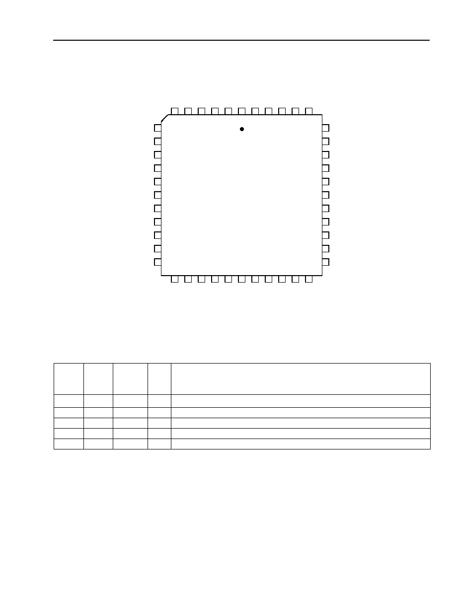
Pin Information
12-3361(F).a
Figure 3. 44-Pin PLCC Pin Diagram
Table 1. Pin Descriptions
* On the printed-wiring board (PWB), make the leads to BGND and V
BAT
as wide as possible for thermal and electrical reasons. Also, maxi-
mize the amount of PWB copper on all leads connected to this device for the lowest operating temperature.
Note: I
u
and O
u
indicate a pull-up device is included on this lead.
Pin,
Circuit
a
Pin,
Circuit
b
Symbol
Type
Name/Function
1
1
V
BAT
*
--
Office Battery Supply. Negative high-voltage power supply, nominally ≠65 V.
44
2
CF2
--
Filter Capacitor 2. Connect 0.22
µ
F capacitor to AGND.
43
3
CF1
--
Filter Capacitor 1. Connect 0.22
µ
F capacitor to AGND.
42
4
BGND
*
--
Battery Ground. Ground return for the battery supply and fault ground.
41
5
B2
I
u
State Input. Refer to Operating States section. A pull-up device is included.
7
9
10
11
12
13
14
15
16
17
8
6
4
3
2
1
44
43
42
41
40
5
18
20
21
22
23
24
25
26
27
28
19
39
37
36
35
34
33
32
31
30
29
38
NDISCa
PTa
RPWRa
VITRa
TG2a
TG1a
RTFLTa
RTTHa
PTb
RPWRb
NDISCb
VITRb
TG2b
TG1b
RTFLTb
RTTHb
RCV
Pb
NSTATb
PRb
PRa
RNGNGb
CF1b
CF2b
V
BA
T
BGNDb
B2b
CF2a
CF
1a
B
G
NDa
B2a
R
N
GN
Ga
NSTATa
DC
OUT
RCV
Nb
I
PRO
G
a
RCVP
a
RCV
Na
V
CC
a
I
PRO
G
b
V
CC
b
AGNDb
AGNDa
DC
OUT
b
RRNG
a

6
Agere Systems Inc.
Data Sheet
May 2001
L8576B Dual Ringing SLIC
Pin Information
(continued)
Table 1. Pin Descriptions (continued)
* On the printed-wiring board (PWB), make the leads to BGND and V
BAT
as wide as possible for thermal and electrical reasons. Also, maxi-
mize the amount of PWB copper on all leads connected to this device for the lowest operating temperature.
Note: I
u
and O
u
indicate a pull-up device is included on this lead.
Pin,
Circuit
a
Pin,
Circuit
b
Symbol
Type
Name/Function
40
6
RNGNG
I
u
Ringing Input. Refer to Operating States section. A pull-up device is
included.
39
7
NSTAT
O
u
Loop Detector Output/Ring Trip Detector Output. When low, this lead indi-
cates an off-hook condition. When in ringing mode, a low output on this lead
indicates a ring trip. A pull-up device is included.
38
8
NDISC
I
u
Disconnect Input. Refer to Operating States section. A pull-up device is
included.
37
9
RPWR
--
Power Resistor. Connect a resistor between this pin and V
BAT
. A 2.2 k
, 2 W
resistor should be used for a V
BAT
of ≠68.5 V. See the Applications section to
calculate resistor values for other V
BAT
potentials.
36
10
PT
I/O
Protected Tip. The input to the tip fault protection and output of tip current
drive amplifier. Connect this pin to the tip of the loop through a 30
overvolt-
age protection resistor.
35
11
PR
I/O
Protected Ring. The input to the ring fault protection and output of ring cur-
rent drive amplifier. Connect this pin to the ring of the loop through a 30
overvoltage protection resistor.
34
12
VITR
O
Transmit ac Output Voltage. This output is a voltage that is directly propor-
tional to the differential tip/ring current.
33
13
TG2
--
Transmit Gain 2. Transmit gain and current limiting for ringing is set by the
value of R
GX2
. R
GX2
is connected between TG2 and VITR.
32
14
TG1
--
Transmit Gain 1. Transmit gain is set by the series resistor combination of
R
GX1
and R
GX2
from this lead to TG2.
31
15
RTFLT
--
Ring Trip Filter. Connect this lead to RTTH via a resistor and to AGND with a
capacitor to filter the ring trip circuit to prevent spurious responses.
30
16
RTTH
--
Ring Trip Threshold. Connect this lead to DC
OUT
via a resistor to set the ring
trip threshold.
29
17
DC
OUT
O
dc Voltage Out. This output is a voltage that is directly proportional to the
absolute value of the differential tip/ring current.
28
18
I
PROG
I
Current-Limit Program Input. A resistor to DC
OUT
sets the dc current limit of
the circuit.
27
19
RCVP
I
Receive Signal Input (+). This high-impedance input controls the ac differen-
tial voltage on tip/ring.
26
20
RCVN
I
Receive Signal Input (≠). This high-impedance input controls the ac differen-
tial voltage on tip/ring.
25
21
AGND
--
Analog Signal Ground.
24
22
V
CC
--
Analog 5 V Power Supply.
23
23
RRNG
--
Ringing Slope Resistor. Connect this lead to AGND with a resistor to set the
slope of the ringing waveform. Note that this pin is shared with both sections.

Agere Systems Inc.
7
Data Sheet
May 2001
L8576B Dual Ringing SLIC
Functional Description
Refer to the architectural and application diagrams
(Figures 1 and 2, respectively).
General
The L8576B is a dual subscriber line interface circuit
with each half of the device providing battery feed,
supervision, and balanced ringing. It is designed to
support short loops, typically on customer premises.
The use of a single battery for both battery feed and
ringing makes this device particularly advantageous
where it is desirable to minimize power supply costs in
small systems, such as terminal adapters. The tip and
ring drive amplifiers are used with a very relaxed cur-
rent limit to develop a trapezoidal, balanced ringing sig-
nal. Use of a nominal ≠65 V power supply allows for
ringing of normal phones, whether equipped with a
mechanical ringer, or a peak-detection type of ringing
detector. While balanced ringing is not the norm world-
wide, its use in short, customer premises loops is gain-
ing popularity.
In addition to the ringing and battery functions, the
L8576B device provides the ac receive and transmit
paths. Also, integral within the device is an off-hook
detection circuit and a ring trip detection circuit that
have their outputs multiplexed on a single lead.
Thermal protection within the device is also provided,
and an external resistor is used to drop the high battery
voltage before applying loop current, thus allowing a
significant portion of the power to be dissipated outside
of the device. Removing much of this power makes it
possible to incorporate two complete circuits in a
44-pin, surface-mount package.
Protection
The L8576B contains some overvoltage protection in
addition to the thermal protection within the device.
This protection, along with the associated tip and ring
protection resistors, may be sufficient in some benign
environments. However, if power line cross or lightning
protection is desired, the use of an external protection
circuit (such as the L7591 device from Agere) is highly
recommended.
The integrated thermal protection consists of a thermal
shutdown circuit which places the tip/ring drivers in a
high-impedance state when the temperature of the die
exceeds 160 ∞C. In thermal shutdown, all supervision
states are undefined.
Tip/Ring Drivers
The L8576B has two tip/ring drivers whose outputs are
PT and PR. Each driver operates as a current source
capable of sinking or sourcing adequate ac signal bias
current. In the normal talk operating mode, these driv-
ers are current-limited at a nominal 24 mA to minimize
the power dissipation of short loops. These amplifiers
are also used to drive balanced ringing. During ringing,
the current limit is raised to approximately 85 mA.
The external resistor connected to the R
PWR
pin is used
to dissipate power externally and also to drop the bat-
tery voltage which is higher than normal in order to
support balanced ringing. Note that this external power
dissipation is present during both ringing or normal bat-
tery feed operation. Power limitations restrict the dual
device to actively ringing only one channel at a time;
thus, ringing cadence must be used to ensure that only
one channel is actively ringing at any given instant of
time. In other words, to ring both channels at the same
time, ring each channel during the quiet interval of the
other channel.
Battery Operation
There are two V
BAT
inputs to the device. Pin 1 (V
BAT
)
provides voltage to the entire SLIC and pins 9 and 37
(R
PWR
) provide voltage to the individual tip and ring
amplifiers of each channel through R
PWR
resistors. A
shared current sourcing scheme is employed within the
device. For loop currents below 20 mA, the V
BAT
applied to pin 1 sources all of the loop current in addi-
tion to driving internal circuitry. For loop currents
greater than 20 mA, loop current is primarily provided
through the R
PWR
resistors and the pin 1 V
BAT
mainly
powers internal circuitry. The R
PWR
resistors can be
replaced by a lower-voltage auxiliary battery. Operation
with an auxiliary battery is described in the Applications
section of this document.
Transmit and Receive Interface
The interface is suitable for direct coupling to a ±5 V
only codec. When interfacing a 5 V only codec, cou-
pling capacitors are required.
The transmit interface circuitry couples the differential
voltage on tip and ring to transmit output VITR. The
inverting input of the driving amplifier is available on
lead TG1, so connecting a resistance between VITR
and TG1 allows adjustment of the transmit gain
(transconductance).

8
8
Agere Systems Inc.
Data Sheet
May 2001
L8576B Dual Ringing SLIC
Functional Description
(continued)
Transmit and Receive Interface
(continued)
A second gain setting is provided to accommodate ring
trip. A switch is built into TG2. In ringing mode, TG1
and TG2 are internally connected, thus shorting out the
external gain resistor R
GX1
. This provides a lower trans-
mit gain for ringing since ring trip is accomplished by
monitoring the voltage at DC
OUT
. This lower gain sets
DC
OUT
at the appropriate level to accommodate the
higher currents of the ring trip.
The receive interface circuitry couples the differential
signal on receive inputs RCVP and RCVN to the
tip/ring drivers.
Data Interface
A 4-wire parallel interface (B2, RNGNG, NDISC, and
NSTAT) is provided for each channel to control signals
to and from the system controller. B2 controls the for-
ward/reverse battery in normal talk mode while
RNGNG enables the balanced ringing mode of opera-
tion, and NDISC performs a disconnect state. NSTAT
reflects either the loop detector output or the ring trip
detector output, depending on the mode of the section.
It is the responsibility of the system controller to recog-
nize ring trip detection and set RNGNG to a logic 0
state to terminate ringing. The system controller should
also use RNGNG to set ringing cadence.
Loop Current Detector
Each section of the device has an integral loop current
detector set at a nominal 12 mA of dc current. This is
used to detect off-hook transitions in the normal talk
state. When current less than the current threshold
(including no current) is flowing, NSTAT is at logic 1.
When loop current exceeds 12 mA, the output NSTAT
switches to a logic 0. No hysteresis is included.
Operating States
The L8576B device has four operating states:
s
Talk state--normal battery:
-- Normal talk state.
-- Battery feed is connected to the battery supply
(V
BAT
).
-- Both receive and transmit transmission paths are
powered up.
-- dc loop and instantaneous current limiters are
powered up and active.
-- NSTAT reflects the status of the switchhook
detector.
-- PR is negative with respect to PT.
s
Talk state--reverse battery:
-- Normal talk state.
-- Battery feed is connected to the battery supply
(V
BAT
).
-- Both receive and transmit transmission paths are
powered up.
-- dc loop current limiter is powered up and active.
-- NSTAT reflects the status of the switchhook
detector.
-- PR is positive with respect to PT.
s
Ringing state:
-- Normal ringing state.
-- Both receive and transmit transmission paths are
inactive.
-- Balanced ringing is applied to PR and PT, in
accordance with B2.
-- Current limiter is set for ringing limit.
-- NSTAT reflects the status of the ring trip detector.
-- Only one channel should be in this state at a time
to control power dissipation.
s
Disconnect state:
-- Tip and ring drive amplifiers are powered down.
-- Pins PT and PR are high impedance (>100 k
).
-- NSTAT is undefined.
-- PT and PR voltage is undefined.

Agere Systems Inc.
9
Data Sheet
May 2001
L8576B Dual Ringing SLIC
Operating States
(continued)
These states are selected using three logic inputs, B2, RNGNG, and NDISC. B2 sets normal operation, either with
forward or reverse battery. RNGNG overrides B2 and applies ringing with the polarity of tip and ring reversed on
edges of the B2 signal. The slope of the waveform is determined by a resistor from RRNG to AGND. Logic input
NDISC puts the device into a loop current denial state (disconnect). Tip and ring amplifiers are saturated against
ground with about a 100
µ
A current source. This creates a level in the loop current sensing circuitry that
approaches a loop closed state. Some conditions on the tip and ring could cause the circuit to indicate loop closed
even though the loop is open. This situation can be prevented by connecting a 300 k
resistor from V
BAT
to each of
the outputs of the tip and ring amplifiers (see Figure 2). This will pull the amplifier output to about 30 V above V
BAT
,
keeping the NSTAT output at a steady high (on-hook indication) level. If the disconnect state is not used or the
NSTAT output during the disconnect state is not recognized or used, then the resistors are not needed.
Table 2 below summarizes the operating input state coding.
Absolute Maximum Ratings
(at T
A
= 25
∞
C)
Stresses in excess of the absolute maximum ratings can cause permanent damage to the device. These are abso-
lute stress ratings only. Functional operation of the device is not implied at these or any other conditions in excess
of those given in the operational sections of the data sheet. Exposure to absolute maximum ratings for extended
periods can adversely affect device reliability.
Note: The IC can be damaged unless all ground connections are applied before, and removed after, all other connections. Furthermore, when
powering the device, the user must guarantee that no external potential creates a voltage on any pin of the device that exceeds its rat-
ings. For example, inductance in a supply lead could resonate with the supply filter capacitor to cause a destructive overvoltage.
Table 2. Input State Coding
NDISC
RNGNG B2
State
1
0
1
Forward Battery, Normal Talk, and Feed State. Pin PT is positive with respect to PR.
1
0
0
Reverse Battery, Normal Talk, and Feed State. Pin PT is negative with respect to PR.
1
1
1
Ringing Is Applied to PT and PR. On the transition, PT starts towards a positive volt-
age (with respect to PR). The endpoint of this state is PT at BGND and PR at V
BAT
.
1
1
0
Ringing Is Applied to PT and PR. On the transition, PT starts towards a negative volt-
age (with respect to PR). The endpoint of this state is PT at V
BAT
and PR at BGND.
0
0/1
0/1 Disconnect State. The tip and ring amplifiers are turned off, and the SLIC goes into a
high-impedance state (>100 k
).
Parameter Symbol
Min
Typ
Max
Unit
5 V dc Supplies
V
CC
≠0.5
--
7.0
V
Office Battery Supply
V
BAT
≠75
--
0.5 V
Logic Input Voltage
--
≠0.5
--
V
CC
+ 0.5
V
Logic Input Clamp Diode Current, per Pin
--
--
±
20
--
mA
Logic Output Voltage
--
≠0.5
--
V
CC
+ 0.5
V
Logic Output Current, per Pin
--
--
±
35
--
mA
Analog Input Voltage
--
≠7.0
--
7.0
V
Maximum Junction Temperature
--
--
165
--
∞
C
Storage Temperature Range
T
stg
≠40
--
125
∞
C
Relative Humidity Range (noncondensing)
--
5
--
95
%
Ground Potential Difference (BGND to AGND)
--
--
±
3
--
V
PT or PR Fault Voltage (dc)
--
V
BAT
≠ 5
--
3
V
PT or PR Fault Voltage (10 µs x 1000 µs)
--
V
BAT
≠ 15
--
15
V

10
Agere Systems Inc.
Data Sheet
May 2001
L8576B Dual Ringing SLIC
Electrical Characteristics
Generally, minimum and maximum values are testing requirements. However, some parameters may not be tested
in production because they are guaranteed by design and device characterization. Typical values reflect the design
center or nominal value of the parameter; they are for information only and are not a requirement. Minimum and
maximum values apply across the entire temperature range (0 ∞C to 70 ∞C) and entire battery range (to ≠72 V).
Unless otherwise specified, typical values are defined as 20 ∞C, V
CC
= 5.0 V, V
BAT
= ≠68.5 V. Positive currents flow
into the device.
Table 3. Operating Conditions and Powering
1. Noncondensing.
2. The L8576B will operate below ≠24 V; ≠24 V is used for production test.
3. The termination impedance can be programmed up to 1200
; 1000
are used for production test.
4. This parameter is not tested in production. It is guaranteed by design and device characterization.
Table 4. Ring Trip Detector
1
1. This table is provided for information purposes only.
2. These parameters are not tested in production.
Parameter
Min
Typ
Max
Unit
Temperature Range
0
--
70
∞
C
Humidity Range
5
--
95
1
%RH
Supply Voltages:
V
CC
V
BAT
4.75
≠24
2
5.0
≠65
5.25
≠72
V
V
Loop Closure Threshold--Detection Range
9.5
12
14.5
mA
ac Termination Impedance Programming Range
300
600
1000
3
On- and Off-hook 2-wire Signal Level
--
3.14
--
dBm
Power Supply--Powerup, No Loop Current (per section):
I
CC
I
BAT
(V
BAT
= ≠65 V)
Total power (one channel, V
BAT
= ≠65 V)
--
--
--
4.5
3.0
230
5.5
4.0
290
mA
mA
mW
Power-supply Rejection (See Figures 6 and 7.):
V
CC
(1 kHz)
V
BAT
(500 Hz--3 kHz)
35
45
--
--
--
--
dB
dB
Thermal
4
:
Thermal Resistance (still air) T
j
Operating T
j
Thermal Shutdown Temperature
--
--
--
47
--
160
--
150
--
∞
C/W
∞
C
∞
C
Parameter
2
Min
Typ
Max
Unit
Ringing Source:
Frequency (
) R
RNG
= 28.7 k
,
R
TTH
= 52.3 k
Frequency (
) Contact Agere for Specific Component Values
17
20
20
--
23
50
Hz
Hz
C-message Weighted Noise (900
)
--
--
90
dBrnC
REN Load (1386
+ 40
µ
F) with Loop Resistance = 30
,
R
PT
= 30
,
R
PR
= 30
--
--
40
Vrms
Detection Interval:
20 Hz
25 Hz
--
--
--
--
200
150
ms
ms
Agere Systems Inc.
11
Data Sheet
May 2001
L8576B Dual Ringing SLIC
Electrical Characteristics
(continued)
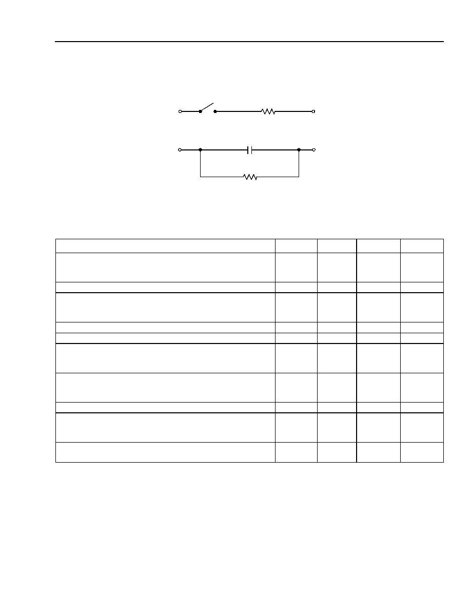
Pretrip will not occur for the circuits shown below, per GR-909, 4.5.9.
12-2572(F).d
Figure 4. Pretrip Circuit
Table 5. Battery Feed
1. Assumes 2 x 30
external protection resistors. Note the useful range of the device may be determined by the ringing or supervision range
rather than the ac characteristics.
2. The longitudinal current is independent of dc loop current.
3. Current limit I
LIM
is programmed by a resistor, R
PROG
, from pin I
PROG
to pin DC
OUT
R
PROG
(k
)
= 3.5 x (I
LIM
≠ 9.2) mA. The current limit has a
slope vs. loop voltage of 6 k
. To control power dissipation, it is recommended that the default current limits be utilized, i.e., R
PROG
= 51.1 k
for 24 mA nominal loop current limit.
4. Instantaneous current limit minimizes inrush current at the onset of an off-hook condition. Inrush current is only limited when in the forward
battery state. The device will settle into a dc loop current-limit value within 400 ms after off-hook.
5.
IEEE
is a registered trademark of The Institute of Electrical and Electronics Engineers, Inc.
6. Assumes the external protection resistors are matched to 1%.
7. This parameter is not tested during production. It is guaranteed by design and device characterization.
Parameter
Min
Typ
Max
Unit
Loop Resistance Range
1
(3.17 dBm overload into 600
):
I
LOOP
= 20 mA at V
BAT
= ≠65 V
1000
--
--
Longitudinal Current Capability per Wire
2
8.5
15
--
mArms
Current Limit
3
R
LOOP
= 100
:
dc Loop
Instantaneous
4
20
50
24
60
28
70
mA
mA
Tip or Ring Drive Current = dc + Longitudinal + Signal Currents
65
--
--
mA
Signal Current
5
--
--
mArms
Powerup Open Loop Voltage Level
Differential Voltage (RNGNG = 0, NDISC = 1, B2 = 1,
V
BAT
= ≠65 V)
|V
BAT
+ 10|
--
--
V
Disconnect State:
PT or PR Current (V
BAT
< V
PT
< 0 V)
PT or PR Resistance (V
BAT
< V
PT
< 0 V)
≠1
100
--
--
1
--
mA
k
dc Feed Resistance
--
60
70
Longitudinal to Metallic Balance--
IEEE
5
Standard 455
6
:
200 Hz to 1 kHz
1 kHz to 3 kHz
54
48
67
62
--
--
dB
dB
Metallic to Longitudinal (Harm) Balance
7
:
200 Hz to 4 kHz
35
--
--
dB
RING
RING
10 k
6
µ
F
TIP
TIP
200
SWITCH CLOSES FOR LESS THAN 12 ms

12
12
Agere Systems Inc.
Data Sheet
May 2001
L8576B Dual Ringing SLIC
Electrical Characteristics
(continued)
Table 6. Analog Signal Pins
Table 7. ac Feed Characteristics
1. Requires external components connected as shown in the Applications section. Transmission characteristics are specified assuming a 600
resistive termination and
±
1% external resistors.
2. Transmission characteristics are specified assuming a 600
resistive termination; however, feedback using external components allows the
user to adjust the termination impedance from 600
. Any complex impedance R1 + R2 || C between 300
and 1000
can be synthesized
using external components.
3. This parameter is not tested in production. It is guaranteed by design and device characterization.
Parameter
Min
Typ
Max
Unit
Differential PT/PR Current Sense (DC
OUT
)
Gain (PT/PR to DC
OUT
):
Forward Battery (R
GX1
= 16.9 k
, R
GX2
= 7.5 k
)
Reverse Battery (R
GX1
= 16.9 k
, R
GX2
= 7.5 k
)
≠235
235
≠250
250
≠265
265
V/A
V/A
PT/PR to VITR Gain with
R
GX1
= 16.9 k
, R
GX2
= 7.5 k
:
Forward Battery
Reverse Battery
≠121
121
≠125
125
≠129
129
V/A
V/A
Loop Closure Detector Threshold:
Programming Accuracy
--
--
±
20
%
RCVN, RCVP:
Input Bias Current
Gain RCVP to PT/PR
Gain RCVN to PT/PR
--
11.62
≠11.62
--
12
≠12
≠1.0
12.38
≠12.38
µ
A
--
--
RCVN, RCVP Input Compliance
≠2.5
--
V
CC
V
Parameter
1
Min
Typ
Max
Unit
ac Termination Impedance
2
300
600
1000
Total Harmonic Distortion (200 Hz--4 kHz)
3
:
Off-hook
On-hook
--
--
--
--
0.3
1.0
%
%
Transmit Gain (
= 1 kHz) (See Figure 5.):
Transmit Accuracy in Percent
Transmit Accuracy in dB (relative to 2/3)
≠3.0
≠0.24
0
0
3.0
0.24
%
dB
Receive Gain (
= 1 kHz) (See Figure 5.):
Receive Accuracy in Percent
Receive Accuracy in dB
≠3.0
≠0.24
0
0
3.0
0.24
%
dB
Tip/Ring Signal Level (600
reference)
--
--
3.14
dBm
Gain vs. Frequency (transmit and receive; 1 kHz reference)
3
:
200 Hz--3.4 kHz
300 Hz--3.4 kHz
3.4 kHz--20 kHz
3.4 kHz--266 kHz
≠1.00
≠0.30
≠3.0
--
0
0
≠0.1
--
0.05
0.05
2.0
2.0
dB
dB
dB
dB

Agere Systems Inc.
13
Data Sheet
May 2001
L8576B Dual Ringing SLIC
Electrical Characteristics
(continued)
Table 7. ac Feed Characteristics (continued)
1. Requires external components connected as shown in Figure 2. Transmission characteristics are specified assuming a 600
resistive ter-
mination and
±
1% external resistors.
2. This parameter is not tested in production. It is guaranteed by design and device characterization.
3. Return loss and transhybrid loss are functions of device gain accuracies and the external hybrid circuit. Guaranteed performance assumes
1% tolerance components.
Table 8. Isolation Between Channels
1. These parameters are not tested in production. They are guaranteed by design and device characterization.
Table 9. Data Interface and Logic
1. All logic voltages are referenced to AGND.
Parameter
1
Min
Typ
Max
Unit
Gain vs. Level (transmit and receive; 0 dBV reference)
2
:
≠50 dB to +3 dB
≠0.05
0
0.05
dB
Return Loss
3
:
200 Hz--500 Hz
500 Hz--3400 Hz
20
26
24
29
--
--
dB
dB
Transhybrid Loss
3
:
200 Hz--500 Hz
500 Hz--2500 Hz
2500 Hz--3400 Hz
20
26
26
24
29
29
--
--
--
dB
dB
dB
Idle-channel Noise (Tip/Ring):
Psophometric
2
C-message
3 kHz Flat
2
--
--
--
--
--
--
≠77
12
20
dBmp
dBrnC
dBrn
Idle-channel Noise (XMT):
Psophometric
2
C-message
3 kHz Flat
2
--
--
--
--
--
--
≠77
12
20
dBmp0
dBrnC0
dBrn0
Parameter
1
Min
Typ
Max
Unit
Interchannel Small-signal Crosstalk. (Both channels in forward or reverse
battery state.) (2-wire to 2-wire, 2-wire to 4-wire, 4-wire to 4-wire.)
--
≠90
≠80
dB
Impulse Noise. (One channel ringing, other channel in forward or reverse
battery state.)
--
40
47
dBrnC0
Parameter
1
Symbol
Min
Typ
Max
Unit
High-level Input Voltage (B2, RNGNG, and NDISC)
V
IH
2
--
V
CC
V
Low-level Input Voltage (B2, RNGNG, and NDISC)
V
IL
0
--
0.7
V
Input Bias Current (high) (B2, RNGNG, and NDISC)
I
IH
≠40
--
≠100
µ
A
Input Bias Current (low) (B2, RNGNG, and NDISC)
I
IL
≠75
--
≠200
µ
A
High-level Output Voltage (NSTAT, open collector with inter-
nal pull-up resistor):
(I
OUT
= ≠20
µ
A)
(I
OUT
= ≠1
µ
A)
V
OH
V
OH
2.4
--
4.3
5.0
V
CC
--
V
V
Low-level Output Voltage (NSTAT, open collector with internal
pull-up resistor) (I
OUT
= 200
µ
A)
V
OL
0
0.2
0.4
V
14
Agere Systems Inc.
Data Sheet
May 2001
L8576B Dual Ringing SLIC
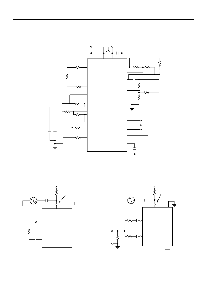
Test Configurations
12-3360(F)a
Figure 5. Basic Test Circuit
B2
V
BAT
V
BAT
BGND V
CC
AGND
V
CC
0.1
µ
F
0.1
µ
F
PT
I
PROG
TG1
VITR
RNGNG
CF1
0.22
µ
F
RCVP
RCVN
0.22
µ
F
CF2
R
LOOP
L8576
SLIC
25
TIP
600
PR
25
RING
R
PROG
DC
OUT
51.1 k
RTTH
RTFLT
RPWR
RRNG
2.2 k
V
BAT
383 k
52.3 k
0.056
µ
F
0.1
µ
F
R
GX1
7.5 k
R
GX2
16.9 k
TG2
XMT
88.7 k
442 k
RCV
NSTAT
28.7 k
R
PT
R
PR
R
PWR
R
RNG
R
TTH
R
TFLT
C
F2
C
F1
R
RCV
R
G
127 k
R
T1
R
GX3
10 k
C
TG
100 pF
0.22
µ
F
12-2582a(F)
Figure 6. Metallic PSRR
12-2583a(F)
Figure 7. Longitudinal PSRR
V
S
4.7
µ
F
100
V
BAT
OR
V
CC
DISCONNECT
V
T/R
V
BAT
OR
V
CC
PT
PR
BASIC
TEST CIRCUIT
+
≠
PSRR = 20log
V
S
V
T/R
900
BYPASS CAPACITOR
V
S
4.7
µ
F
100
V
BAT
OR
V
CC
DISCONNECT
BYPASS CAPACITOR
56.3
V
BAT
OR V
CC
PT
PR
BASIC
TEST CIRCUIT
PSRR = 20log
V
S
V
M
67.5
10
µ
F
10
µ
F
67.5
V
M
+
≠

Agere Systems Inc.
15
Data Sheet
May 2001
L8576B Dual Ringing SLIC
Test Configurations
(continued)
LONGITUDINAL BALANCE = 20log
12-2584(F)b
Figure 8. Longitudinal Balance
12-2585(F).r1
Figure 9. Longitudinal Impedance
12-2587(F)
Figure 10. ac Gains
Applications
Characteristic Curves
Figures 11--16 display typical room temperature read-
ings.
12-3507(F)
Note: Gain is normalized to 0 dB.
Figure 11. Receive Gain and Hybrid Balance vs.
Frequency
12-3508
Note: Gain is normalized to 0 dB.
Figure 12. Transmit Gain and Return Loss vs.
Frequency
TIP
RING
BASIC
TEST CIRCUIT
365
100
µ
F
100
µ
F
365
V
M
+
≠
V
S
V
S
V
M
-------
PT
PR
BASIC
TEST CIRCUIT
+
≠
+
≠
I
LONG
I
LONG
V
PT
V
PR
Z
LONG
=
OR
V
PT
I
LONG
V
PR
I
LONG
PT
PR
BASIC
TEST CIRCUIT
600
V
T/R
+
≠
G
XMT
=
V
XMT
V
T/R
G
RCV
=
V
T/R
V
RCV
XMT
RCV
V
S
FREQUENCY (Hz)
0.1k
100k
≠30
≠20
≠10
10k
≠60
≠50
≠40
1k
DE
CI
BELS
(
d
B)
0
HYBRID BALANCE
RECEIVE GAIN
FREQUENCY (Hz)
0.1k
100k
≠35
≠20
≠10
10k
≠50
≠45
≠40
1k
DE
CI
B
E
LS
(dB
)
RETURN LOSS
TRANSMIT GAIN
≠5
≠15
≠25
≠30
≠55
0
16
Agere Systems Inc.
Data Sheet
May 2001
L8576B Dual Ringing SLIC
Applications
(continued)
Characteristic Curves
(continued)
12-3503 (F)
Note: R
PROG
= 51.1 k
.
Figure 13. Loop Current vs. Loop Voltage
12-3506 (F)
Note: R
PROG
= 51.1 k
.
Figure 14. Loop Current vs. Loop Resistance
12-3504 (F)
Figure 15. SLIC Power Dissipation vs. Loop
Resistance (V
BAT
= ≠48 V)
12-3505 (F)
Figure 16. SLIC Power Dissipation vs. Loop
Resistance (V
BAT
= ≠65 V)
10
20
30
40
50
0
LOOP VOLTAGE (V)
15
50
60
0
10
5
45
40
35
30
25
20
L
O
OP CURRENT
(
m
A)
V
BAT
= ≠65 V
V
BAT
= ≠48 V
0
15
50
10
5
45
40
35
30
25
20
200
400
600
800
1000
LOOP RESISTANCE (
)
2000
0
L
OOP CURRENT
(
m
A)
1200 1400 1600 1800
V
BAT
= ≠48 V
V
BAT
= ≠65 V
200
400
600
800
1000
0
LOOP RESISTANCE (
)
500
1500
2000
0
1000
SL
I
C
PO
WE
R
DI
SSI
PA
TI
O
N
(
m
W)
1200 1400 1600 1800
2 CH
1 CH
200
400
600
800
1000
0
LOOP RESISTANCE (
)
500
1500
2000
0
1000
S
L
IC P
O
W
E
R DI
S
S
IP
A
T
ION (
m
W
)
1200 1400 1600 1800
2 CH
1 CH
Agere Systems Inc.
17
Data Sheet
May 2001
L8576B Dual Ringing SLIC
Applications
(continued)
dc Design
Battery Feed
The dc feed characteristic can be described by:
Where:
I
L
= dc loop current.
V
T/R
= dc loop voltage.
|V
BAT
| = battery voltage magnitude.
V
OH
= overhead voltage. This is the difference between
the battery voltage and the open loop tip/ring
voltage.
R
L
= loop resistance, not including protection resistors.
R
P
= protection resistor value.
R
dc
= SLIC internal dc feed resistance.
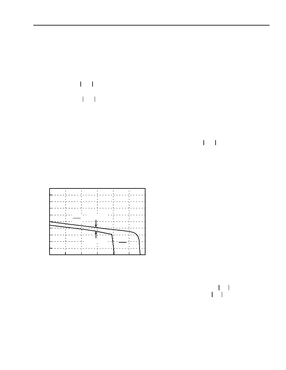
The design begins by drawing the desired dc template.
An example is shown in Figure 17.
12-3503.a (F)
Figure 17. Loop Current vs. Loop Voltage
Starting from the on-hook condition and going through
to a short circuit, the curve passes through two regions:
Region 1: On-hook and low loop currents. In this
region, the slope corresponds to the dc resistance of
the SLIC, R
dc
(typically 60
). The open circuit voltage
is the battery voltage less the overhead voltage of the
device, V
OH
(default is 7.1 V typical). These values are
suitable for most applications.
Region 2: Current limit. The dc current is limited to a val-
ue determined by external resistor R
PROG
. This region of
the dc template has a high resistance (6 k
).
Calculate the external resistor as follows:
R
PROG
(k
) = 3.5 x (I
LIM
≠ 9.2) mA
*
To control power dissipation, it is recommended that a
51.1 k
R
PROG
resistor be used to set a default current-
limit value of 24 mA.
R
PWR
The R
PWR
resistors dissipate the excess power associ-
ated with a single power supply, short-loop application.
The resistor provides V
BAT
to tip and ring amplifiers.
There is one resistor associated with each channel.
The value of R
PWR
is dependent upon the battery
potential and the current-limit value. The value of R
PWR
can be determined by using the following equation:
R
PWR
=
Power dissipation of the resistor is:
W
RPWR
= (I
LIM
≠ 0.003)
2
R
PWR
.
For the recommended ≠68.5 V V
BAT
and 24 mA I
LIM
design, a 2.2 k
, 2 W resistor is suitable. 2 W resistors
are available as surface-mount components.
Overhead Voltage
In order to drive an on-hook ac signal, the SLIC must
set up the tip and ring voltage to a value less than the
battery voltage. The amount that the open loop voltage
is decreased relative to the battery is referred to as the
overhead voltage and is expressed as:
V
OH
=
|
V
BAT
|
≠ (V
PT
≠ V
PR
)
Without this buffer voltage, amplifier saturation will
occur and the signal will be clipped. The L8576 is auto-
matically set at the factory to allow undistorted on-hook
transmission of a 3.17 dBm signal into a 900
loop
impedance.
The drive amplifiers are capable of 4 Vrms minimum
(V
AMP
). So, the maximum signal the device can guaran-
tee is:
For normal forward or reverse battery operation, over-
head voltage is internally set to about 8 V. In ringing
mode, the overhead voltage is automatically decreased
to about 4 V to permit passage of a larger ring signal.
* During the balanced ringing mode, the current limit is increased
from the value predicted by this equation by a factor of 3.5.
I
L
V
B A T
V
O H
≠
R
L
2R
P
R
d c
+
+
----------------------------------
=
V
T/R
V
B AT
V
O H
≠
(
)
R
L
◊
R
L
2R
P
R
d c
+
+
--------------------------------------------
=
10
20
30
40
50
0
LOOP VOLTAGE (V)
15
50
60
0
10
5
45
40
35
30
25
20
L
OOP CUR
RE
NT
(
m
A)
V
BAT
= ≠65 V
V
BAT
= ≠48 V
1
6 k
≠1
Rdc
V
B AT
22.3
≠
I
L I M
0.003
≠
-----------------------------
V
T/R
4 V
Z
T/R
Z
T/R
2R
P
+
--------------------------
=
18
18
Agere Systems Inc.
Data Sheet
May 2001
L8576B Dual Ringing SLIC
Applications
(continued)
dc Design
(continued)
Off-Hook Detection
The loop closure comparator has built-in longitudinal
rejection, eliminating the need for an external 60 Hz fil-
ter. The loop closure detection threshold is internally
set at 12 mA.
Power Ringing
The L8576B is designed to generate a balanced trape-
zoidal power ring signal to tip and ring. Because the
L8576B generates the power ringing signal, no ring
relay is needed in this mode of operation. Alternatively,
the L8576B SLIC can be used in a battery-backed,
unbalanced ringing application. In this case, the ring
signal is generated by a central ring generator and is
bused to individual tip/ring pairs. A ringing relay is used
during ringing to disconnect the L8576B from, and
apply the ring generator to, the tip and ring pair.
This section discusses in detail the use of the L8576B
in the balanced mode of operation.
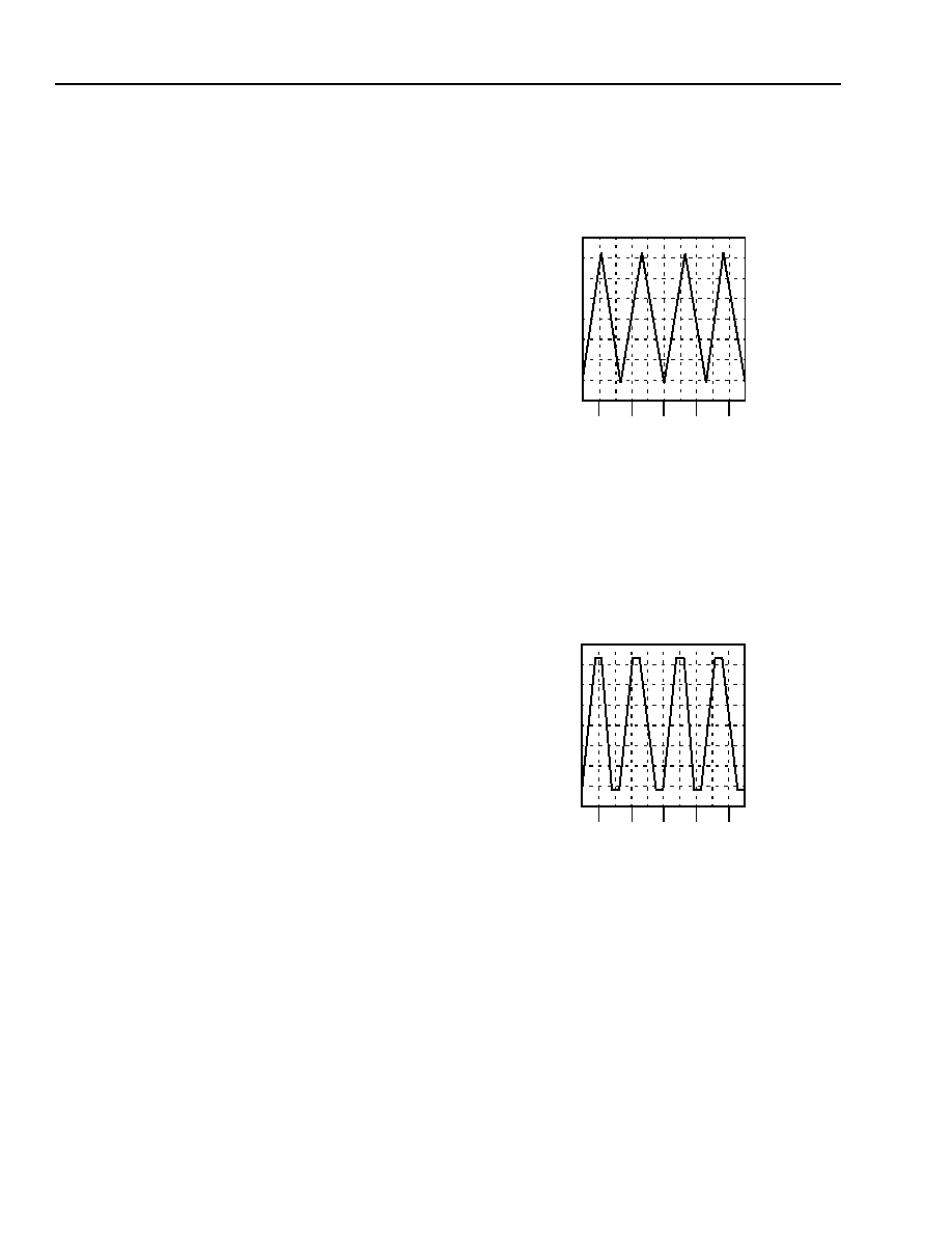
Crest Factor
The balanced ring signal is generated by simply tog-
gling between the powerup forward and reverse battery
states. The state change is done by applying a square
wave (whose frequency is the desired ring frequency)
to logic input B2. Capacitors CF1 and CF2 and resistor
R
RNG
are used to control or ramp the speed of the tran-
sition of the battery reverse, thus shaping the balanced
ring signal. Setting capacitor CF1 = CF2 = 0.22
µ
F and
setting R
RNG
to 28.7 k
provides a crest factor of 1.3
for a 20 Hz ring frequency. This satisfies the
Telcordia
*
GR-909 requirement of ringing waveform crest factor
between 1.2 and 1.6. Crest factor is defined as the
peak to rms voltage ratio of the ring signal. Ringing
waveforms of crest factors 1.6 and 1.2 are shown in
Figures 18 and 19. The crest factor can be adjusted by
the value of R
RNG
and will be influenced slightly by the
value of V
BAT
. The CF1 and CF2 capacitors should not
be changed because these affect the dc feedback loop
stability in current limit. An R
RNG
value of 22.6 k
will
lower the crest factor to about 1.2 with a ≠65 V or
≠72 V battery for a 20 Hz ring frequency. Likewise, an
R
RNG
value of 34.8 k
will raise the crest factor to
about 1.4. For ring frequencies greater than 20 Hz, the
R
RNG
value should be lowered until the desirable crest
factor is achieved. Note the RRNG is common to both
sections of the device.
CF1 and CF2 must exhibit a stable capacitance value
over its voltage range to ensure a properly shaped
waveform. Do not use a ceramic capacitor for CF1 and
CF2; use a capacitor with a polyester, polypropylene,
polycarbonate, or polystyrene dielectric.
12-3346a (F)
Notes:
Slew rate = 5.65 V/ms.
trise = tfall = 23 ms.
pwidth = 2 ms.
period = 50 ms.
Figure 18. Ringing Waveform Crest Factor = 1.6
12-3347a (F)
Notes:
Slew rate = 10.83 V/ms.
trise = tfall = 12 ms.
pwidth = 13 ms.
period = 50 ms.
Figure 19. Ringing Waveform Crest Factor = 1.2
*
Telcordia
is a registered trademark of Telcordia Technologies, Inc.
TIME (s)
≠80
≠60
≠40
≠20
0
20
40
60
80
0.00
0.02 0.06
0.04 0.08
0.10
0.12
0.14
0.16
0.18
0.20
VO
L
T
S (
V
)
TIME (s)
≠80
≠60
≠40
≠20
0
20
40
60
80
0.00
0.02 0.06
0.04 0.08
0.10
0.12
0.14
0.16
0.18
0.20
VOL
T
S
(V
)

Agere Systems Inc.
19
Data Sheet
May 2001
L8576B Dual Ringing SLIC
Applications
(continued)
Power Ringing
(continued)
Power Ringing Load
Telcordia
GR-909 specifies that a minimum 40 Vrms
must be delivered to a 5 REN ringing load of 1386
+
40
µ
F. For 5 REN load, it is recommended that V
BAT
be
set to ≠68.5 Vdc. During the power ring state, the dc
current limit is automatically boosted by a factor of 3.5
over the current limit set by resistor R
PROG
. Both of
these factors are necessary to ensure delivery of
40 Vrms to the North American 5 REN ringing load of
1386
+ 40
µ
F.
Ring Trip
Ring trip is accomplished by filtering the voltage seen
at node DC
OUT
and applying it to the integrated ring trip
comparator. DC
OUT
is a voltage proportional to the tip/
ring current, and under short dc loop conditions, on-
hook ringing current and off-hook current provide suffi-
cient voltage differential at DC
OUT
to distinguish that a
ring trip condition has occurred. The ring trip compara-
tor threshold is set via a resistor between the ring trip
comparator and DC
OUT
.
The output of NSTAT is automatically set to detect ring
trip during the balanced ring mode. During quiet inter-
vals of ringing, the output of NSTAT is automatically
determined by the loop closure detector.
Refer to Figure 2 for the following discussion.
Capacitor C
RT
in conjunction with resistor R
TFLT
form a
single-pole, low-pass filter that smooths the voltage
seen at DC
OUT
. The pole of the filter will influence both
the ripple seen at DC
OUT
and the speed of the transi-
tion of the voltage at DC
OUT
from the pretrip to the
tripped level.
To determine the low-pass pole:
f(Hz) =
Using the recommended 383 k
R
TFLT
resistor and
the 0.1 µF C
RT
capacitor, the low-pass pole is set at
4.15 Hz.
The loop current at ring trip is given by:
I
LOOP(TRIP)
= 7.76 mA
Using the recommended 52.3 k
R
TTH
resistor and the
7.5 k
R
GX2
resistor in a 20 Hz ringing application, the
ring trip threshold current is set for 54 mA.
Reference Design for ISDN TA Applications
For a complete reference design, please refer to the
POTS for ISDN, WLL, and FITL/FITH Applications,
Featuring Ringing SLIC Solutions
Application Note,
which provides a detailed discussion of the reference
design functionality. The design presented utilizes a dc
to dc converter and requires only a +5 V and a +12 V
supply to operate. The schematic in Figure 2 of this
document portrays the SLIC and codec portions of that
design.
ac Design
There are four key ac design parameters. Termination
impedance is the impedance looking into the 2-wire
port of the line card. It is set to match the impedance of
the telephone loop in order to minimize signal reflec-
tions back to the telephone set. Transmit gain is mea-
sured from the 2-wire port to the PCM highway, while
receive gain is measured from the PCM highway to
the 2-wire port or telephone loop. Finally, the hybrid
balance circuit cancels the unwanted amount of the
received signal that appears at the transmit port.
1
2
R
TFLT
(
)
C
RT
(
)
-----------------------------------------------
R
TTH
R
GX2
---------------

20
20
Agere Systems Inc.
Data Sheet
May 2001
L8576B Dual Ringing SLIC
Applications
(continued)
ac Design
(continued)
Example 1, Real Termination
The following design equations refer to the circuit in
Figure 20. Use these to synthesize real termination
impedance.
Termination impedance:
Receive gain:
Transmit gain:
Hybrid balance:
To optimize the hybrid balance, the sum of the currents
at the VF
X
IN input of the codec op amp should be set
to 0. The following expressions assume the hybrid bal-
ance network is the same as the termination imped-
ance:
Z
t
V
T/R
I
T/R
≠
----------
=
Z
t
2R
P
1500
1
R
T 1
R
G P
---------
R
T 1
R
R C V
------------
+
+
-----------------------------------
+
=
G
R C V
V
T/R
V
F R O
-----------
=
G
RC V
12
1
R
R CV
R
T 1
-----------
R
R C V
R
G P
------------
+
+
1
Z
t
Z
T/R
---------
+
------------------------------------------------------------------
=
G
TX
V
GSX
V
T/R
---------------
=
G
TX
R
X
R
T2
----------
125
Z
T/R
-----------
◊
=
h
b a l
20
V
G SX
V
T/R
-----------
log
=
R
H B
R
X
G
RC V
G
T X
◊
--------------------------
=
h
b a l
20
R
X
R
H B
---------
G
R C V
G
T X
◊
≠
log
=
12-2554.o (F)
Figure 20. ac Equivalent Circuit Using a T8503 Codec
R
P
Z
T
+
≠
R
P
V
T/R
I
T/R
V
S
Z
T/R
+
≠
PR
A
V
= ≠1
A
V
= 1
VITR
≠
+
+
≠
CURRENT
SENSE
PT
TG
R
GX
+
≠
R
T1
R
RCV
R
HB
R
T2
RCVN
RCVP
RX
GSX
VF
X
IN
VF
R
O
1/2 T8503 CODEC
R
GP
+2.4 V
125 V/A
1/2 L8576
SLIC
AX
A
V
= 6
Agere Systems Inc.
21
Data Sheet
May 2001
L8576B Dual Ringing SLIC
Applications
(continued)
ac Design
(continued)
Example 2, Complex Termination
The gain shaping required of a complex termination
impedance can be synthesized using the internal AX
amplifier. The following discussion and equations
present a method for selecting proper component val-
ues for the SLIC/codec interface when using a complex
termination.
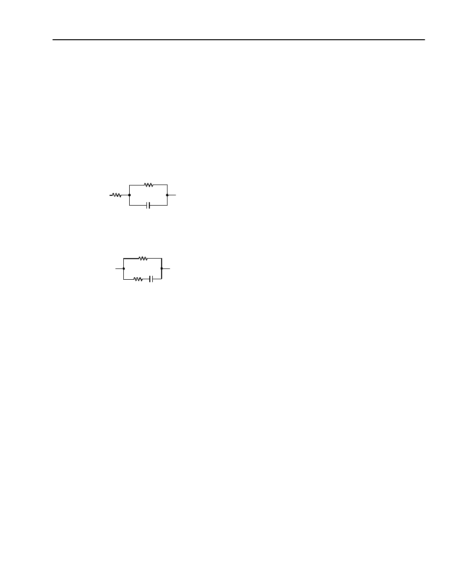
Complex termination is usually of the form:
5-6396(F)
To work with this application, convert termination to the
form:
5-6397(F)
where:
R
1
¥ = R
1
+ R
2
R
2
¥ =
(R
1
+ R
2
)
C¥ =
C
For the following discussion, refer to Figure 21.
R
TGP
/R
TGS
/C
TGS
(Z
TG
): These components give gain
shaping to get good gain flatness. These components
are a scaled version of the specified complex termina-
tion impedance. Note for pure (600
) resistive termi-
nations, components R
TGS
and C
TGS
are not used.
Resistor R
TGP
is used and is the series resistance com-
bination of R
GX1
and R
GX2
or 24.4 k
.
R
X
/R
T2
: With other components set, the transmit gain
(for complex and resistive terminations) R
X
and R
T2
are
varied to give specified transmit gain.
R
T1
/R
RCV
/R
GP
: For both complex and resistive termina-
tions, the ratio of these resistors set the receive gain.
For resistive terminations, the ratio of these resistors
set the return loss characteristic. For complex termina-
tions, the ratio of these resistors set the low-frequency
return loss characteristic.
C
N
/R
N1
/R
N2
: For complex terminations, these compo-
nents provide high-frequency compensation to the
return loss characteristic. For resistive terminations,
these components are not used. R
CVN
is connected to
ground via a resistor.
R
HB
: Sets hybrid balance for all terminations.
Set Z
TG
-- gain shaping:
Z
TG
= R
TGP
|| R
TGS
+ C
TGS
which is a scaled version of
Z
T/R
(the specified termination resistance) in the
R
1
¥ || R
2
¥ + C¥ form.
R
TGP
must be 24.4 k
to set SLIC transconductance to
125 V/A.
R
TGP
= 24.4 k
At dc, C
TGS
and C¥ are open.
R
TGP
= M x R1¥
where M is the scale factor.
M =
It can be shown:
R
TGS
= M x R2¥
and
C
TGS
=
R
2
C
R
1
R
1
¥
C¥
R
2
¥
R
1
R
2
-------
R
2
R
1
R
2
+
---------------------
2
24.4 k
R
1
------------------------
C
M
------
22
Agere Systems Inc.
Data Sheet
May 2001
L8576B Dual Ringing SLIC
Applications
(continued)
ac Design
(continued)
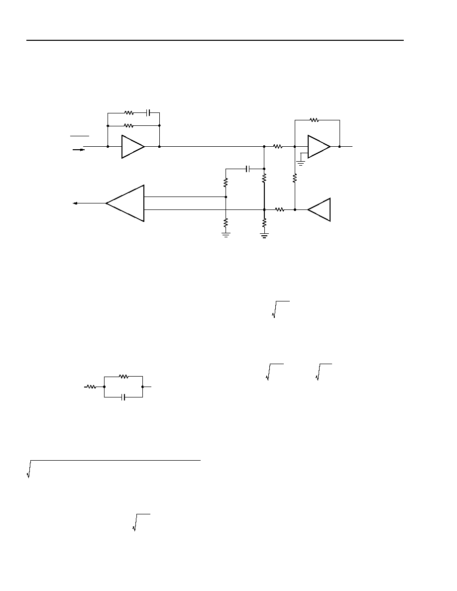
5-6400a(F)
Figure 21. ac Interface Circuit Using First-Generation Codec (Blocking Capacitors Not Shown)
R
TGS
R
TGP
= 24.4 k
V
ITR
R
T2
R
x
R
T1
R
HB
CODEC
OUTPUT
DRIVE
AMP
CODEC
OP AMP
≠
+
C
N
R
N1
R
N2
R
GP
R
RCV
RCVN
RCVP
≠I
T/R
195
C
TGS
AX
Transmit Gain
Transmit gain will be specified as a gain from T/R to
PCM, T
X
(dB). Since PCM is referenced to 600
and
assumed to be 0 dB, and in the case of T/R being refer-
enced to some complex impedance other than 600
resistive, the effects of the impedance transformation
must be taken into account.
Again specified complex termination impedance at T/R
is of the form:
5-6396(F)
First calculate the equivalent resistance of this network
at the midband frequency of 1000 Hz.
R
EQ
=
Using R
EQ
, calculate the desired transmit gain, taking
into account the impedance transformation:
T
X
(dB) = T
X (specified[dB])
+ 20log
T
X (specified[dB])
is the specified transmit gain. 600
is the
impedance at the PCM and R
EQ
is the impedance at
the T/R. 20log
represents the power loss/gain
due to the impedance transformation.
Note in the case of a 600
pure resistive termination
at T/R 20log
= 20log
= 0.
Thus, there is no power loss/gain due to impedance
transformation and T
X
(dB) = T
X (specified[dB])
.
Finally, convert T
X
(dB) to a ratio, G
TX
:
T
X
(dB) = 20log G
TX
The ratio of R
X
/R
T2
is used to set the transmit gain:
= G
TX
x
with a dual Agere codec such as T8503
R
X
< 200 k
R
2
C
R
1
2
f
(
)
2
C
12
R
1
R
22
R
1
R
2
+
+
1
2
f
(
)
2
R
22
C
12
+
-----------------------------------------------------------------------------
2
2
f
R
22
C
1
1
2
f
(
)
2
R
22
C
12
+
---------------------------------------------------
2
+
600
R
EQ
-----------
600
R
EQ
-----------
600
R
EQ
-----------
600
600
----------
R
X
R
T2
----------
195
M
----------

Agere Systems Inc.
23
Data Sheet
May 2001
L8576B Dual Ringing SLIC
Applications
(continued)
ac Design
(continued)
Receive Gain
Ratios of R
RCV
, R
T1
, R
GP
will set both the low-frequency
termination and receive gain for the complex case. In
the complex case, additional high-frequency compen-
sation, via C
N
, R
N1
, and R
N2
, is needed for the return
loss characteristic. For resistive termination, C
N
, R
N1
,
and R
N2
are not used and R
CVN
is tied to ground and a
resistor.
Determine the receive gain, G
RCV
, taking into account
the impedance transformation in a manner similar to
transmit gain.
R
X
(dB) = R
X (specified[dB])
+ 20log
R
X
(dB) = 20log G
RCV
Then:
G
RCV
=
and low-frequency termination
Z
TER(low)
=
+ 2R
P
R
EQ
600
-----------
6
1
R
RCV
R
T1
---------------
R
RCV
R
GP
---------------
+
+
------------------------------------------------
1500
1
R
T1
R
GP
------------
R
T1
R
RCV
---------------
+
+
--------------------------------------------
Z
TER(low)
is the specified termination impedance assum-
ing low frequency (C or C¥ is open).
R
P
is the series protection resistor.
These two equations are best solved using a computer
spreadsheet.
Next, solve for the high-frequency return loss compen-
sation circuit, C
N
, R
N1
, and R
N2
:
C
N
x
R
N2
=
C
TGS
x
R
TGP
R
N1
= R
N2
There is an input offset voltage associated with nodes
R
CVN
, R
CVP
. To minimize the effect of the mismatch of
this voltage at T/R, the equivalent resistance to ac
ground at R
CVN
should be approximately equal to that
at R
CVP
. Refer to Figure 22 (schematic with dc blocking
capacitors). To meet this requirement, R
N2
= R
GP
|| R
T1
.
Hybrid Balance
Set the hybrid cancellation via R
HB
.
R
HB
=
If a +5 V only codec such as an Agere T8503 is used,
dc blocking capacitors must be added as shown in
Figure 22. This is because the codec is referenced to
+2.5 V and the SLIC to ground. With the ac coupling, a
dc bias at T/R is eliminated and power associated with
this bias is not consumed.
2R
P
1500
-------------
1500
2R
P
-------------
R
T GS
R
T GP
--------------
1
≠
R
X
G
RCV
G
TX
◊
----------------------------------
5-8413 (F)
Figure 22. ac Interface Circuit Using First-Generation Codec (Including Blocking Capacitors)
R
TGS
R
TSP
= 24.4 k
V
ITR
R
X
R
HB
CODEC OUTPUT
DRIVE AMP
CODEC
OP AMP
≠
+
C
C1
R
T1
R
GP
R
N2
R
RCV
RCVN
RCVP
≠I
T/R
195
C
TGS
C
B
AX
C
C2
C
N
R
N1
R
T2

24
24
Agere Systems Inc.
Data Sheet
May 2001
L8576B Dual Ringing SLIC
Applications
(continued)
ac Design
(continued)
Typically, values of 0.1
µ
F to 0.47
µ
F capacitors are
used for dc blocking. The addition of blocking capaci-
tors will cause a shift in the return loss and hybrid bal-
ance frequency response toward higher frequencies,
degrading the lower-frequency response. The lower
the value of the blocking capacitor, the more pro-
nounced the effect is, but the cost of the capacitor is
lower. It may be necessary to scale resistor values
higher to compensate for the low-frequency response.
This effect is best evaluated via simulation. A
PSPICE
*
model for the L8576B is available.
Design equation calculations seldom yield standard
component values. Conversion from the calculated
value to standard value may have an effect on the ac
parameters. This effect should be evaluated and opti-
mized via simulation.
Use of an Auxiliary Battery Supply
A second lower-voltage battery supply can be used
with the L8576B in order to lower the overall power
consumption on a short-loop design. For long loops,
any power savings will be negated, since long loops
are supplied by the main battery voltage. The auxiliary
battery would be connected to pins 9 and 37 in lieu of
the R
PWR
resistors. When the external R
PWR
resistors
are removed, more power will be dissipated in the SLIC
so internal SLIC power dissipation must be examined.
First, determine the auxiliary battery voltage:
The auxiliary battery should be set 8 V greater than the
maximum tip/ring loop voltage on the longest allowed
loop, when both channels are off-hook and in current
limit.
Aux Bat
(MAX)
= [(I
LIM
x R
LOOP
) + V
OH
] TOL
VBAT
Where:
I
LIM
= dc current limit set by R
PROG
(usually 0.024).
R
LOOP
= maximum loop resistance supported (tele-
phone plus line resistance plus protection
resistors).
V
OH
= overhead voltage.
TOL
VBAT
= battery tolerance, for a battery tolerance of
±5%, use 1.1.
For example, using the recommended 24 mA current
limit, an overhead voltage of 8 V, and a maximum loop
length of 550
, the maximum auxiliary battery voltage
is 23.3 V.
Next, calculate the power dissipated in the SLIC:
Components of the SLIC power dissipation are quies-
cent power of V
CC
and V
BAT
and loop current associ-
ated with V
BAT
and Aux Bat. These can be calculated
as follows:
W
VCC(quiescent)
= V
CC
x I
CC(Max)(quiescent)
x 2 channels.
W
VBAT(quiescent)
= |V
BAT(Max)
| x I
BAT(Max)(quiescent)
x 2 chan-
nels.
W
VBAT(loop current)
= (|V
BAT(Max)
| ≠ 4 V) x 3 mA x 2 chan-
nels.
W
Aux Bat(loop current)
= (|Aux Bat
(Max)
| ≠ 4 V) x (I
LIM
≠ 3 mA)
x 2 channels.
Where:
4 V is the minimum overhead voltage, and 3 mA is
V
BAT
's contribution to loop current.
For example, substituting values from the data sheet:
V
CC
= 5 V
I
CC(Max)(quiescent)
= 5.5 mA
V
BAT(Max)
= ≠70 V
I
BAT(Max)(quiescent)
= 4 mA
Aux Bat
(Max)
= ≠23.3 V
I
LIM
= 24 mA
The following powers are calculated:
W
VCC(quiescent)
= 5 x 0.0055 x 2 = 0.055
W
VBAT(quiescent)
= |≠70| x 0.004 x 2 = 0.56
W
VBAT(loop current)
= (|≠70| ≠ 4) x 0.003 x 2 = 0.396
W
Aux Bat(loop current)
= (|≠23.3| ≠ 4) x (0.024 ≠ 0.003) x 2 =
0.8106
The sum of the four powers is 1.822 W.
Finally, calculate the maximum ambient tempera-
ture allowed for the calculated power dissipation:
T
A(max)
= T
j
≠ (R
JA
x P
DISS SLIC(max)
)
The L8576's 44-pin PLCC exhibits a 43 ∞C/W thermal
resistance if in an enclosure with natural airflow. The
maximum operating temperature of the SLIC is 150 ∞C.
Thermal shutdown occurs typically at 160 ∞C.
For example:
T
A(max)
= 150 ≠ (43 x 1.822)
= 150 ≠ 78.4
= 71.7 ∞C
The above scenario would allow operation up to 70 ∞C.
*
PSPICE
is a registered trademark of Cadence Design Systems, Inc.

Agere Systems Inc.
25
Data Sheet
May 2001
L8576B Dual Ringing SLIC
Outline Diagram
44-Pin PLCC
Dimensions are in millimeters.
5-2506(F).r8
4.57
MAX
1.27 TYP
0.53
MAX
0.10
SEATING PLANE
0.51 MIN
TYP
1
6
40
7
17
29
39
18
28
PIN #1 IDENTIFIER
ZONE
16.66 MAX
17.65 MAX
16.66
MAX
17.65
MAX

Data Sheet
May 2001
L8576B Dual Ringing SLIC
Agere Systems Inc. reserves the right to make changes to the product(s) or information contained herein without notice. No liab ility is assumed as a result of their use or application.
Copyright © 2001 Agere Systems Inc.
All Rights Reserved
May 2001
DS01-199ALC (Replaces DS01-112ALC)
For additional information, contact your Agere Systems Account Manager or the following:
INTERNET: http://www.agere.com
E-MAIL: docmaster@micro.lucent.com
N. AMERICA:
Agere Systems Inc., 555 Union Boulevard, Room 30L-15P-BA, Allentown, PA 18109-3286
1-800-372-2447, FAX 610-712-4106 (In CANADA: 1-800-553-2448, FAX 610-712-4106)
ASIA PACIFIC: Agere Systems Singapore Pte. Ltd., 77 Science Park Drive, #03-18 Cintech III, Singapore 118256
Tel. (65) 778 8833, FAX (65) 777 7495
CHINA: Agere Systems (Shanghai) Co., Ltd., 33/F Jin Mao Tower, 88 Century Boulevard Pudong, Shanghai 200121 PRC
Tel. (86) 21 50471212, FAX (86) 21 50472266
JAPAN: Agere Systems Japan Ltd., 7-18, Higashi-Gotanda 2-chome, Shinagawa-ku, Tokyo 141, Japan
Tel. (81) 3 5421 1600, FAX (81) 3 5421 1700
EUROPE: Data Requests: DATALINE: Tel. (44) 7000 582 368, FAX (44) 1189 328 148
Technical Inquiries: GERMANY: (49) 89 95086 0 (Munich), UNITED KINGDOM: (44) 1344 865 900 (Ascot),
FRANCE: (33) 1 40 83 68 00 (Paris), SWEDEN: (46) 8 594 607 00 (Stockholm), FINLAND: (358) 9 3507670 (Helsinki),
ITALY: (39) 02 6608131 (Milan), SPAIN: (34) 1 807 1441 (Madrid)
Ordering Information
Device Part No. Description Package Comcode
LUCL8576BP-D Dual SLIC 44-Pin PLCC (Dry-bagged) 108131285
LUCL8576BP-DT Dual SLIC 44-Pin PLCC (Tape and Reel, Dry-bagged) 108131293