 | –≠–ª–µ–∫—Ç—Ä–æ–Ω–Ω—ã–π –∫–æ–º–ø–æ–Ω–µ–Ω—Ç: L9312 | –°–∫–∞—á–∞—Ç—å:  PDF PDF  ZIP ZIP |

Data Sheet
July 2001
L9312 Line Interface and Line Access Circuit
Forward Battery SLIC and Ringing Relay for TR-57 Applications
Introduction
The Agere Systems Inc. L9312 is a combination full-
feature, ultralow-power SLIC, and solid-state ringing
access relay. It is part of a pin-for-pin compatible
family of devices designed to serve a wide variety of
applications. The L9312 is optimized for TR-57
access, forward battery only, applications.
Features
SLIC
s
5 V and battery operation
s
Optional automatic battery switch
s
Four operational modes
s
Appropriate for 58 dB longitudinal balance applica-
tions
s
Minimal external components required at all inter-
faces
s
Ultralow power dissipation
s
Software/hardware adjustable dc parameters and
supervision thresholds
Solid-State Ring Relay
s
Low impulse noise
s
Current-limited switches/thermal protection
Applications
s
Pair Gain
s
Digital Loop Carrier (DLC)
s
Central Office (CO)
s
Fiber-in-the-Loop (FITL)
Description
The L9312 electronic line interface and line access
circuit (LILAC) provides all the functions that are nec-
essary to interface a codec to the tip and ring of a
subscriber loop, integrating the battery feed and ring-
ing access relay in one low-power, low-cost package.
The L9312 requires a 5 V and battery supply to oper-
ate. Included is an automatic battery switch. The
battery feed offers forward battery and on-hook
transmission. It also has a low-power scan and a dis-
connect mode.
In all operating states, this IC is designed for minimal
power dissipation. This device is designed to mini-
mize the number of external components required at
all interfaces.
The dc template, current limit, and overhead voltage
and loop supervision threshold are programmable via
an applied voltage source. The voltage source may
be an external programmable voltage source or
derived from the V
REF
SLIC output.
The integrated solid-state switch offers power ringing
access. Impulse noise is minimized, thus eliminating
the need for external zero-cross switching circuitry.

Data Sheet
July 2001
Forward Battery SLIC and Ringing Relay for TR-57 Applications
L9312 Line Interface and Line Access Circuit
2
Agere Systems Inc.
Table of Contents
Contents
Page
Introduction..................................................................1
Features ....................................................................1
SLIC .......................................................................1
Solid-State Relay....................................................1
Applications...............................................................1
Description ................................................................1
Features ......................................................................4
Description...................................................................4
Architecture .................................................................7
Pin Information ............................................................8
Operating States........................................................10
Input State Coding ..................................................10
State Definitions ........................................................11
Primary Control Modes ...........................................11
Powerup, Forward Battery....................................11
Scan .....................................................................11
Ringing .................................................................11
Disconnect--Break Before Make .........................11
Reset ....................................................................11
Special States .........................................................11
Thermal Shutdown ...............................................11
Battery Out of Range ...........................................12
Absolute Maximum Ratings ......................................12
Electrical Characteristics ...........................................13
Ring Trip Detector ...................................................14
SLIC Two-Wire Port ................................................15
Analog Pin Characteristics ......................................16
ac Feed Characteristics ..........................................17
Logic Inputs and Outputs, V
DD
= 5.0 V ...................18
Timing Requirements ..............................................18
Switch Characteristics.............................................19
On-State Switch I-V Characteristics........................20
Test Configurations ...................................................21
Applications ...............................................................23
dc Characteristics ...................................................23
Power Control.......................................................23
Power Derating.....................................................23
Automatic Battery Switch .....................................24
Contents
Page
Power Control Resistor ....................................... 24
Overhead Voltage ............................................... 25
dc Loop Current Limit .......................................... 26
Loop Range......................................................... 26
Battery Feed ........................................................ 26
Longitudinal to Metallic Balance.......................... 27
Supervision ............................................................... 27
Loop Closure.......................................................... 27
Ring Trip ................................................................ 28
Switching Behavior................................................. 28
Make-Before-Break Operation ............................... 28
Break-Before-Make Operation ............................... 29
Protection ................................................................. 29
External Protection................................................. 29
Active Mode Response at PT/PR........................... 29
Ring Mode Response at PT/PR ............................. 30
Internal Tertiary Protection..................................... 31
Diode Bridge........................................................ 31
Battery Out of Range Detector: High
(Magnitude) ................................................. 31
Battery Out of Range Detector: Low
(Magnitude) ................................................. 31
ac Applications ......................................................... 32
ac Parameters........................................................ 32
Codec Types .......................................................... 32
ac Interface Network .............................................. 32
Design Tools .......................................................... 33
First-Generation Codec ac Interface Network........ 33
First-Generation Codec ac Interface
Network: Resistive Termination ............................ 34
Example 1, Real Termination .............................. 35
Third-Generation Codec ac Interface
Network: Complex Termination ............................ 38
Outline Diagram........................................................ 40
Ordering Information................................................. 40

Data Sheet
July 2001
Forward Battery SLIC and Ringing Relay for TR-57 Applications
L9312 Line Interface and Line Access Circuit
Agere Systems Inc.
3
Table of Contents
(continued)
Figures
Page
Figure 1. Architecture Diagram................................... 7
Figure 2. 44-Pin PLCC ............................................... 8
Figure 3. Timing Requirements ................................ 18
Figure 4. On-State Switch I-V Characteristics .......... 20
Figure 5. Basic Test Circuit ...................................... 21
Figure 6. Metallic PSRR ........................................... 22
Figure 7. Longitudinal PSRR .................................... 22
Figure 8. Longitudinal Balance ................................. 22
Figure 9. Longitudinal Impedance ............................ 22
Figure 10. ac Gains .................................................. 22
Figure 11. L9312 Loop/Battery Current (with Battery
Switch) vs. Loop Resistance ................... 24
Figure 12. Tip/Ring Voltage ..................................... 26
Figure 13. L9312 Loop Current vs. Loop Voltage..... 27
Figure 14. ac Equivalent Circuit................................ 34
Figure 15. Agere T7504 First-Generation
Codec Resistive Termination, Single
Battery Operation .................................... 36
Figure 16. L9312 for Agere T8536 Third-Generation
Codec, Dual Battery Operation, ac and dc
Parameters, Fully Programmable............ 38
Tables
Page
Table 1. Pin Descriptions ........................................... 8
Table 2. Control States ............................................. 10
Table 3. Supervision Coding..................................... 10
Table 4. Device Operating Conditions and
Powering ..................................................... 13
Table 5. Ring Trip Detector ....................................... 14
Table 6. SLIC Two-Wire Port .................................... 15
Table 7. Analog Pin Characteristics .......................... 16
Table 8. ac Feed Characteristics .............................. 17
Table 9. Logic Inputs and Outputs ............................ 18
Table 10. Timing Requirements ................................ 18
Table 11. Break Switches (SW1, 2) .......................... 19
Table 12. Ring Return Switch (SW3) ........................ 19
Table 13. Ringing Access Switch (SW4) .................. 20
Table 14. Typical Active Mode On- to Off-Hook
Tip/Ring Current-Limit Transient
Response .................................................. 26
Table 15. Break-Before-Make Logic Control
Sequence Device Switching...................... 29
Table 16. L9312 Parts List for Agere T7504
First-Generation Codec Resistive Termina-
tion, Single Battery Operation ................... 37
Table 17. L9312 Parts List for Agere T8536
Third-Generation Codec, Dual Battery
Operation, ac and dc Parameters, Fully
Programmable........................................... 39

Data Sheet
July 2001
Forward Battery SLIC and Ringing Relay for TR-57 Applications
L9312 Line Interface and Line Access Circuit
4
Agere Systems Inc.
Features
s
SLIC and solid-state ring relay integrated into a sin-
gle package
s
5 V and battery operation
s
User-defined power control options:
-- Automatic battery switch
-- Power control resistor
-- Package thermal capabilities
s
Minimal external components required
s
Operating states:
-- Forward active
-- Scan
-- All-off or disconnect
-- Ring
s
Ultralow power:
-- Scan, 15 mW
-- Active states, on-hook, 75 mW
-- Ring mode, on-hook, 90 mW
-- Disconnect, 10 mW
s
Adjustable overhead voltage:
-- Default overhead adequate for 3.14 dB into
900
overload
-- Controlled rate of overhead adjustment
s
Latched parallel input data interface with reset
s
Adjustable current limiter:
-- 10 mA to 45 mA programming range
s
Adjustable loop closure detector with hysteresis:
-- 4 mA detect, 2.5 mA no detect minimum, upper
limit of 15 mA detect
-- Hysteresis, typical 20% of programmed on-hook
to off-hook threshold
s
Ring trip detector:
-- Single-pole filtering
s
Thermal shutdown protection with hysteresis
s
Line break switch will foldover into a low-current
state under high-voltage fault conditions
s
Battery out-of-range monitor circuit:
-- All-off upon loss of battery (low battery condition)
-- All-off upon high battery (fault condition)
s
Longitudinal balance:
-- TR-57 balance
s
RFI/EMC-CISP-22
s
Integrated 2 Form C ring relay:
-- Low impulse noise
-- Current-limited switches
-- Break-before-make and make-before-break
switching
s
Meets
Telcordia Technologies
* GR1089 require-
ments with external protection device
s
44-pin, surface-mount plastic package (PLCC)
Description
The L9312 electronic line interface and line access cir-
cuit (LILAC) provides all the functions that are neces-
sary to interface a codec to the tip and ring of a
subscriber loop, integrating the battery feed and ringing
access relay in one low-power, low-cost package. The
physical construction of the device is two chips. The
first chip is manufactured in Agere 90 V complemen-
tary bipolar integrated circuit (CBIC-S) technology. This
chip contains the SLIC functionality:
s
ac transmission path
s
dc feedback and functions
s
Active dc current limit
s
Active mode loop supervision
s
Thermal shutdown
The second chip is manufactured in Agere dielectrically
isolated 320 V bipolar CMOS diffused metal oxide
semiconductor (BCDMOS III) technology. This chip
contains the following:
s
Ring access relay
s
Scan clamp circuitry
s
Logic control
s
Ring trip
s
Thermal shutdown
s
Battery monitor circuit
The LILAC family requires a +5 V and battery supply to
operate. No ≠5 V supply is required. A battery switch is
included that automatically, based on subscriber loop
length, will apply either the primary higher-voltage bat-
tery or an optional lower-voltage auxiliary battery. Use
of this feature will minimize off-hook power dissipation.
*
Telcordia Technologies
is a trademark of Bell Communications
Research, Inc.

Data Sheet
July 2001
Forward Battery SLIC and Ringing Relay for TR-57 Applications
L9312 Line Interface and Line Access Circuit
Agere Systems Inc.
5
Description
(continued)
The switch point is a function of the user-programmed
dc current limit and the magnitude of the auxiliary bat-
tery. Switching from the high-voltage to low-voltage
battery is quiet, without interruption of the dc loop cur-
rent, thus preventing any impulse noise generation at
the switch point. Design equations for the switch point
and a graph showing loop/battery current versus loop
resistance are given in the dc Characteristics in the
Applications section of this data sheet.
If the user does not want to provide an auxiliary battery,
the design of the L9312 battery switch allows use of a
power control resistor at the auxiliary battery input. This
scheme will not reduce short-loop, off-hook power dis-
sipation, but it will control power dissipation on the
SLIC by sharing power among the SLIC, power resis-
tor, and dc loop. However, in most cases, without the
auxiliary battery, the power dissipation capabilities of
the 44-pin PLCC package are adequate so that the
power control resistor will not be needed. Design equa-
tions for power control options are given in the dc Char-
acteristics section of this data sheet.
The L9312 is a forward battery only SLIC that supports
on-hook transmission.
A low-power scan mode is available to reduce idle
mode on-hook power. This mode is realized by using a
scan clamp circuit. In low-power scan mode:
s
The scan clamp circuitry is active.
s
Loop closure is active.
s
All ac transmission, dc feed, and other supervision
circuits, including ring trip, are shut down.
s
Thermal shutdown is active.
s
Low battery sense shutdown is on.
s
On-hook transmission is disabled.
A forward disconnect mode, where all circuits are
turned off and power is denied to the loop, is also pro-
vided. During this mode, the NSTAT supervision output
will read on-hook.
In the ring mode, the line break switches are opened
and the power ring access switches are closed. In this
mode, the ring trip detector in the SLIC is active and all
other detectors and the tip/ring drive amplifiers are
turned off to conserve power.
Make-before-break or break-before-make switching is
achievable during ring cadence or ring trip. Toggling
directly into or directly out of the ring mode table will
give make-before-break switching. To achieve break-
before-make switching, go to an intermediate all-off
state (use forward disconnect state) before entering the
ring mode or before leaving the ring mode. See the
Switching Behavior section of this data sheet for more
details on switching behavior.
Voltage transients or impulse noise associated with
ring cadence or ring trip are minimized or eliminated
with the L9312, thus possibly eliminating the need for
external zero-cross switching circuitry.
Both the ring trip and loop closure supervision func-
tions are included. Loop closure threshold is set by
applying a voltage source to the LCTH input. The volt-
age source may be an external voltage source or
derived from the SLIC V
REF
output. A programmable
external voltage source may be used to provide soft-
ware control of the loop closure threshold. Design
equations for the loop closure threshold are given in
the Supervision section of this data sheet.
Hysteresis is
included.
The ring trip detector requires only a single-pole filter at
the input. This will minimize the required number of
external components. To help minimize device power
dissipation, the ring trip detector is active only during
the power ring mode.
Ring trip and loop supervision status outputs appear in
a common output pin, NSTAT. NSTAT is an unlatched
supervision output; thus, an interrupt-based control
scheme may be used.
The dc current limit is set in the active modes via an
applied voltage source. The voltage source may be an
external voltage source. The voltage may be derived
via a resistor divider network from the V
REF
SLIC out-
put. A programmable external voltage source may be
used to provide software control of the loop closure
threshold. Design equations for this feature are given in
the dc Characteristics section of this data sheet. Pro-
gramming range is 10 mA to 45 mA.
Overhead is programmable in the active modes via an
applied voltage
source. The voltage source may be an
external voltage source or derived via a resistor divider
network from the V
REF
SLIC output.
A programmable external voltage source may be used
to provide software control of the overhead voltage.
The rate of change of the overhead voltage may be
controlled by use of a single external capacitor at the
C
F1
node. If the rate of change is uncontrolled, there
may be audible noise associated with this transition.
Design equations for this feature are given in the dc
Characteristics section of this data sheet.
If the overhead is not programmed via a resistor, the
device develops a default overhead adequate for a
3.14 dBm overload into 900
. For the default over-
head, OVH is connected to ground.

Data Sheet
July 2001
Forward Battery SLIC and Ringing Relay for TR-57 Applications
L9312 Line Interface and Line Access Circuit
6
Agere Systems Inc.
Description
(continued)
Data control is via a parallel latched data control
scheme. Data latches are edge-level sensitive. Data is
latched in when the LATCH control input goes low.
While LATCH is low, the user cannot change the data
control inputs. The data control inputs may only be
changed when LATCH is high.
Incorporation of data latches allows for data control
information and loop supervision information to be
passed to and from the SLIC via data buses rather than
on a per-line basis, thus minimizing routing complexity
and board routing area.
A device RESET pin is included. When this pin is low,
the logic inputs are overridden and the device will be
reset into SLIC forward disconnect state and the switch
into the all-off state. NSTAT is forced to the on-hook
condition when RESET is low.
The overall device protection is achieved through a
combination of an external secondary protector, along
with an integrated thermal shutdown feature, a battery
voltage window comparator, the break switch foldback
characteristic, and the dc/dynamic current-limit
response of the break and tip return switches.
For protection against long duration fault conditions,
such as power cross and tip/ring shorts, a thermal shut-
down mechanism is integrated into the device. Upon
reaching the thermal shutdown temperature, the device
will enter an all-off mode. Upon cooling, the device will
re-enter the state it was in prior to thermal shutdown.
Hysteresis is built in to prevent oscillation. During this
mode, the NSTAT supervision output overrides the
actual loop status and forces an off-hook.
The line break switches and tip return switch are
current-limited switches. The current-limit mechanism
limits current through the switch to the specified dc cur-
rent limit under low frequency or dc faults (power cross
and/or tip/ring to ground short) and limits the current to
the specified dynamic current-limit response under
transient faults, such as lightning.
A foldover characteristic is incorporated into the line
break switches within their I-V curve. Under voltage
conditions higher than the normal operating range,
such as may be seen under an extreme lightning or
power cross fault condition, the line break switch will
fold over into a low-current state. This feature allows for
more relaxed specifications on the ring side protector,
thus allowing for higher-voltage ringing signals. (Tip
side protector is limited by the requirements on the tip
return switch.) This feature is part of the overall device
protection scheme.
This device uses a window comparator to force an all-
off condition if the battery drops below, or rises above,
a specified threshold.
Upon loss of V
BAT1
, the L9312 will automatically enter
an all-off mode. The device will enter this mode if the
magnitude of the battery drops below a nominal 15 V
and will remain in this mode until the magnitude of the
battery rises above a typical 20 V. During this mode,
the NSTAT supervision output will override the actual
hook status and force an off-hook or logic low.
When the device is in the scan mode, because of the
design of the scan clamp circuit, common-mode cur-
rent can be forced into or out of the battery supply.
Because of this, and depending upon power supply
design, the magnitude of the battery may rise above
the maximum operating condition during extended lon-
gitudinal currents or during a power cross fault condi-
tion. To prevent excess current from being forced into
or out of the battery, if the magnitude of the battery
rises typically above 75 V to 80 V, the device will enter
an all-off state. The device will remain in the all-off state
until the magnitude of the battery drops into the normal
operating range. During this mode, the NSTAT supervi-
sion output will override the actual hook status and
force an off-hook or logic low.
See the Protection section of this data sheet for more
details on device protection. Please contact your Agere
Account Representative for a recommended secondary
protection device.
Longitudinal balance is consistent with North American
TR-57 requirements.
Transmit and receive gains have been chosen to mini-
mize the number of external components required in
the SLIC-codec ac interface, regardless of the choice
of codec.
The L9312 uses a voltage feed, current sense architec-
ture; thus, the transmit gain is a transconductance. The
L9312 transconductance is set via a single external
resistor, and this device is designed for optimal perfor-
mance with a transconductance set at 300 V/A.
The L9312 offers an option for a single-ended to differ-
ential receive gain of either 8 or 2. These options are
mask programmable at the factory and are selected by
choice of part number.
A receive gain of 8 is more appropriate when choosing
a first-generation type codec where termination imped-
ance, hybrid balance, and overall gains are set by
external analog filters. The higher gain is typically
required for synthesization of complex termination
impedance.
Data Sheet
July 2001
Forward Battery SLIC and Ringing Relay for TR-57 Applications
L9312 Line Interface and Line Access Circuit
Agere Systems Inc.
7
Description
(continued)
A receive gain of 2 is more appropriate when choosing
a third-generation type codec. Third-generation codecs
will synthesize termination impedance, set hybrid bal-
ance, and set overall gains. To accomplish these func-
tions, third-generation codecs typically have both
analog and digital gain filters. For optimal signal-to-
noise performance, it is best to operate the codec at a
higher gain level. If the SLIC then provides a high gain,
the SLIC output may be saturated causing clipping dis-
tortion of the signal at tip and ring. To avoid this situa-
tion, with a higher-gain SLIC, external resistor dividers
are used. These external components are not neces-
sary with the lower gain offered by the L9312.
The RCVP/RCVN SLIC inputs are floating inputs. If
there is not feedback from RCVP/RCVN to VITR,
RCVP/RCVN may be directly coupled to the codec out-
put. If there is feedback, RCVP/RCVN must be ac-cou-
pled to the codec output.
This device is packaged in a 44-pin PLCC surface-
mount package.
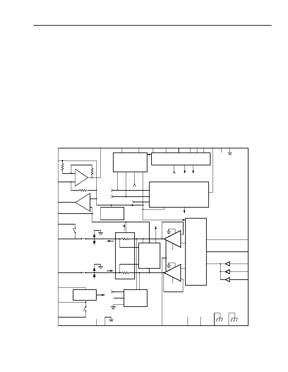
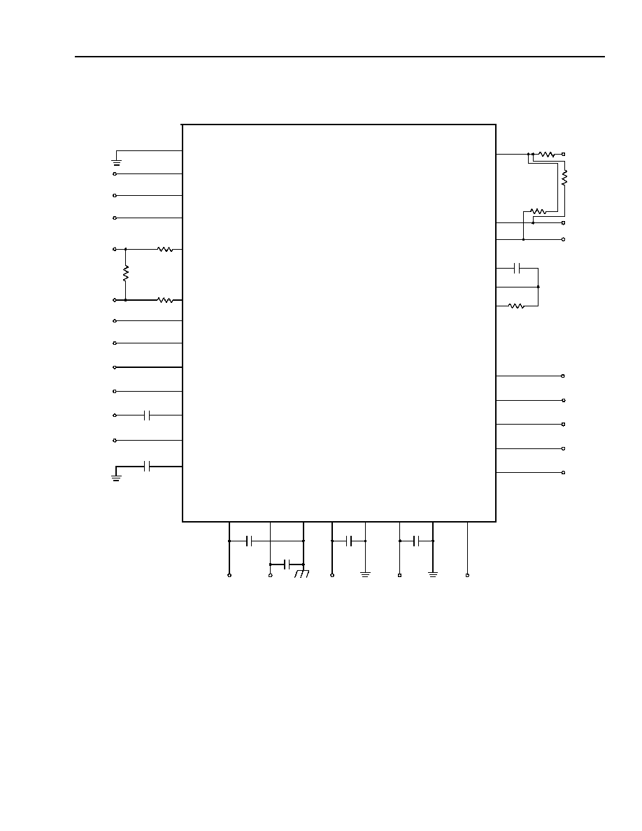
Architecture
12-3523e (F)
Figure 1. Architecture Diagram
≠
+
AAC
+
≠
AX
2.35 V
BANDGAP
REFERENCE
RFT
TIP/RING
CURRENT
SENSE
BGND
ITR/325
RFR
V
BAT
BGND
V
BAT
ITR
ITR
RING TRIP
DETECTOR
SCAN
DETECTOR
SCAN
CLAMP
SCAN
V
BAT
BGND
RT
ILC
ac
INTERFACE
SWITCHHOOK
WINDOW
COMPARATOR
IN
REF
CF2
CURRENT LIMITER
AND
INRUSH CONTROL
CF2
REF
PARALLEL DATA INTERFACE
V
REF
TXI
ITR
TRNG
PT
PR
RTS
RSW
RRING
VTX
V
CC
A
GND
V
BAT2
/PWR
V
BAT
V
BAT1
V
BAT1
BGND
BGND
RCVP
RCVN
CF2
dc
ac
DGND
V
DD
V
PROG
B0
B1
B2
LATCH
RESET
LCTH
LCF
VITR
CONTROL
RT
ILC
FB
RB
VTX
IN
+5V
D
(1 V/50 mA)
SW3
SW1
18
60
SW2
18
+5V
A
V
BAT
V
BAT
BGND
BGND
+
≠
OUT AT
+
≠
OUT AR
NSTAT
2.35 V
V
REF
SW4
15
ac
CF1
OVH
Data Sheet
July 2001
Forward Battery SLIC and Ringing Relay for TR-57 Applications
L9312 Line Interface and Line Access Circuit
8
Agere Systems Inc.
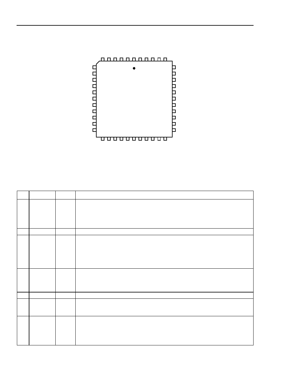
Pin Information
12-3522f (F)
Figure 2. 44-Pin PLCC
Table 1. Pin Descriptions
Pin
Symbol Type
Name/Function
1 LCTH
I
Loop Closure Program Input. Connect a voltage source to this point to program the
loop closure threshold. Voltage source may be external and must be connected
through a resistor, or derived via a resistor divider from V
REF
. A programmable exter-
nal voltage source may be used to provide software control of the loop closure
threshold.
2
V
REF
O
SLIC Internal Reference Voltage. Output of internal 2.35 V SLIC reference voltage.
3
OVH
I
Overhead Voltage Program Input. Connect a voltage source to this point to pro-
gram the overhead voltage. Voltage source may be external or derived via a resistor
divider from V
REF
. A programmable external voltage source may be used to provide
software control of the overhead voltage. If a resistor or voltage source is not con-
nected, the overhead voltage will default to approximately 5.5 V (sufficient to pass
3.14 dBm in to 900
). If the default overhead is desired, connect this pin to ground.
4
V
PROG
I
Current-Limit Program Input. Connect a voltage source to this point to program the
dc current limit. Voltage source may be external or derived via a resistor divider from
V
REF
. A programmable external voltage source may be used to provide software con-
trol of the loop closure threshold.
5
CF2
--
Filter Capacitor. Connect a capacitor from this node for filtering.
6
CF1
--
Filter Capacitor. Connect a capacitor from this node to OVH to control the rate of
change of the overhead voltage. If controlled overhead is not desired, leave this node
open.
7,
8,
17,
18,
34
NC
--
No Connect. May not be used as a tie point.
7
9
10
11
12
13
14
15
16
17
8
6
4
3
2
1 44 43 42 41 40
5
18
20 21 22 23 24 25 26 27 28
19
39
37
36
35
34
33
32
31
30
29
38
L9312AP
10
NC
LCF
RPWR
V
BAT1
V
BAT1
BGND
TIE B
TIE A
NC
NC
BGND
CF
1
V
PR
O
G
OV
H
V
RE
F
LC
T
H
V
CC
AG
N
D
RC
VN
RC
VP
V
ITR
CF
2
TXI
ITR
AGND
NC
DGND
V
DD
LATCH
RESET
B0
NC
VTX
NC
RSW
RRI
NG
PR
PT
TR
IN
G
NST
A
T
DGND
B2
B1
RT
S

Data Sheet
July 2001
Forward Battery SLIC and Ringing Relay for TR-57 Applications
L9312 Line Interface and Line Access Circuit
Agere Systems Inc.
9
Pin Information
(continued)
Table 1. Pin Descriptions (continued)
Pin
Symbol
Type
Name/Function
9
LCF
--
Loop Closure Filter Capacitor. PPM injection can cause false loop closure indication.
Connect a capacitor from this node to V
CC
to filter the loop closure detector. If loop clo-
sure filtering is not required, leave this node open.
10
BGND
G
Battery Ground. Ground return for the battery supply.
11
RPWR
P
Auxiliary Battery. If a lower-voltage auxiliary battery is used, connect the auxiliary bat-
tery supply to this node. If a power control resistor is used, connect the power control
resistor from this node to V
BAT1
. If no power control technique is used, connect this node
to V
BAT1
.
12
V
BAT1
P
Office Battery Supply. Negative high-voltage power supply.
13
V
BAT1
P
Office Battery Supply. Negative high-voltage power supply.
14
BGND
G
Battery Ground. Ground return for the battery supply.
15
TIE B'
--
Connect to V
REF
.
16
TIE A'
--
Connect to V
REF
.
19
RTS
I
Ring Trip Sense. Sense input for the ring trip detector.
20
RSW
O
Ring Lead Ringing Access Switch. Ringing relay connects this pin to pin RRING. Con-
nect this pin to pin PR through a 400
current-limiting resistor.
21
RRING
I
Ringing Access. Input to solid-state ringing access switch. Connect to ringing genera-
tor.
22
PR
I/O
Protected Ring. The output of the ring driver amplifier and input to loop sensing con-
nected through solid-state break switch. Connect to subscriber loop through overvolt-
age/current protection.
23
PT
I/O
Protected Tip. The output of the tip driver amplifier and input to loop sensing connected
through solid-state break switch. Connect to subscriber loop through overvoltage/cur-
rent protection.
24
TRING
O
Tip Ringing Return. Ring relay connects this pin to PT. Connect to ringing supply
return.
25
NSTAT
O
Loop Status. The output of the loop status detector (loop start detector wired-OR with
ring trip detector). This loop status supervision output is not controlled by the data latch.
26
DGND
G
Digital Ground. Ground return for V
DD
current.
27
B2
I
Data Control Input. See Table 2, Control States, for details.
28
B1
I
Data Control Input. See Table 2, Control States, for details.
29
B0
I
Data Control Input. See Table 2, Control States, for details.
30
RESET
I
Reset. A logic low will override the B[0:3] and LATCH inputs and reset the state of the
SLIC to the disconnect state and the switch to the all-off state.
31
LATCH
I
Latch Control Input. Edge-level sensitive control for data latches.
32
V
DD
P
5 V Digital Power Supply. 5 V supply for digital circuitry.
33
DGND
G
Digital Ground. Ground return for V
DD
current.
35
AGND
G
Analog Ground.
36
VTX
O
Tip/Ring Voltage Output. This output is a voltage that is directly proportional to the dif-
ferential tip/ring current. A resistor from this node to ITR sets the device transimped-
ance. Gain shaping for termination impedance with a COMBO I codec is also achieved
with a network from this node to ITR.

Data Sheet
July 2001
Forward Battery SLIC and Ringing Relay for TR-57 Applications
L9312 Line Interface and Line Access Circuit
10
Agere Systems Inc.
Pin Information
(continued)
Table 1. Pin Descriptions (continued)
Operating States
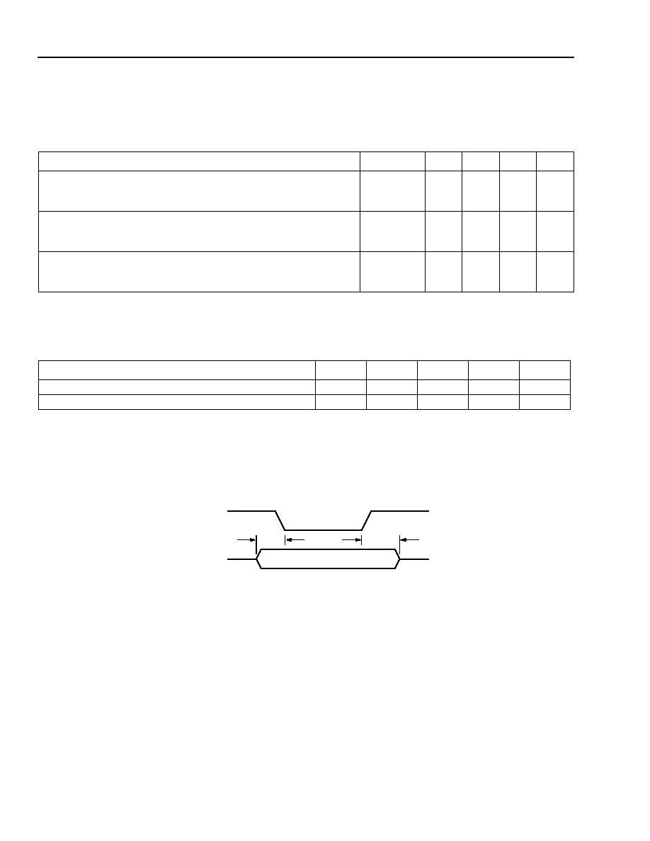
Input State Coding
Data control is via a parallel latched data control scheme. Data latches are edge-level sensitive. Data is latched in
when the LATCH control input goes low. Data must be set up 200 ns before LATCH goes low and held 50 ns after
LATCH goes high. While LATCH is low, the user should not change the data control inputs at B0, B1, and B2. The
data control inputs at B0, B1, and B2 may only be changed when LATCH is high. NSTAT supervision output is not
controlled by the LATCH control input.
Table 2. Control States
Table 3. Supervision Coding
Pin
Symbol
Type
Name/Function
37
ITR
I
Transmit Gain. A current output which is proportional to the differential current flow-
ing from tip to ring. Input to AX amplifier. Connect a resistor from this node to VITR to
set transmit gain to 300
. Gain shaping for termination impedance with a COMBO I
codec is also achieved with a network from this node to VITR.
38
NC
--
No Connect. May not be used as a tie point.
39
TXI
I
Transmit ac Input (Noninverting). Connect a 0.1
µ
F capacitor from this pin to VTX
for dc blocking.
40
VITR
O
Transmit ac Output Voltage. The output is a voltage that is directly proportional to
the differential ac tip/ring current. This output is connected via a proper interface net-
work to the codec.
41
RCVP
I
Receive ac Signal Input (Noninverting). This high-impedance input controls the ac
differential voltage on tip and ring.
42
RCVN
I
Receive ac Signal Input (Inverting). This high-impedance input controls the ac dif-
ferential voltage on tip and ring.
43
AGND
G
Analog Ground. Ground return for V
CC
current.
44
V
CC
P
5 V Analog Power Supply. 5 V supply for analog circuitry.
B2
B1
B0
RESET
State
0
0
0
1
Scan
0
0
1
1
Powerup, forward battery
0
1
0
1
Unassigned
0
1
1
1
Unassigned
1
0
0
1
Ring
1
0
1
1
Unassigned
1
1
0
1
Unassigned
1
1
1
1
Disconnect, break before make
X
X
X
0
Disconnect, break before make
Pin NSTAT
Pin TRGDET
0 = off-hook or ring trip
0 = ring ground
1 = on-hook and no ring trip
1 = no ring ground

Data Sheet
July 2001
Forward Battery SLIC and Ringing Relay for TR-57 Applications
L9312 Line Interface and Line Access Circuit
Agere Systems Inc.
11
State Definitions
Primary Control Modes
Powerup, Forward Battery
s
Normal talk and battery feed state.
s
Pin PT is positive with respect to pin PR.
s
All ac transmission and dc feed circuits are powered
up.
s
On-hook transmission is enabled.
s
Thermal shutdown is active.
s
Battery window comparator sense shutdown is on.
s
Switch break switches (SW1 and SW2) are closed,
and ring access switches (SW3 and SW4) are open.
s
V
BAT1
is applied to tip and ring during on-hook condi-
tions.
s
Automatic battery switch selects V
BAT1
or V
BAT2
dur-
ing off-hook conditions.
s
All supervision circuits except for ring trip detector
are active.
s
NSTAT represents the loop closure detector status.
Scan
s
Scan clamp circuitry is active.
s
Loop closure is active.
s
All ac transmission, dc feed, and other supervision
circuits, including ring trip, are shut down.
s
Thermal shutdown is active.
s
Battery window comparator sense shutdown is on.
s
On-hook transmission is disabled.
s
Pin PT is positive with respect to PR, and V
BAT1
is
applied to tip/ring.
s
Switch break switches (SW1 and SW2) are closed,
and ring access switches (SW3 and SW4) are open.
s
NSTAT represents the loop closure detector status.
Ringing
s
Switch break switches (SW1 and SW2) are open,
and ring access switches (SW3 and SW4) are
closed.
s
Tip/ring drive amplifiers are powered down.
s
Ring trip circuit is active.
s
Loop supervision and common-mode current detec-
tors are powered down.
s
NSTAT represents the ring trip detector status.
Disconnect--Break Before Make
s
The tip and ring amplifiers are turned off to conserve
power.
s
Break switches (SW1 and SW2) are open, and ring
access switches (SW3 and SW4) are open. This
mode is also used as a transitional mode to achieve
break-before-make switching from the power ring to
active or scan mode.
s
All supervision circuits are powered down; NSTAT
overrides the actual loop condition and is forced high
(on-hook).
Reset
s
Selection of device reset via the RESET pin will set
the device into the disconnect break-before-make
state.
Special States
Thermal Shutdown
s
Not controlled via truth table inputs.
s
This mode is caused by excessive heating of the
device, such as may be encountered in an extended
power cross situation.
s
Upon reaching the thermal shutdown temperature,
the device will enter an all-off mode.
s
Upon cooling, the device will re-enter the state it was
in prior to thermal shutdown.
s
Hysteresis is built in to prevent oscillation. In this
mode, supervision output NSTAT is forced low
(off-hook) regardless of loop status or if the discon-
nect logic state is selected.

Data Sheet
July 2001
Forward Battery SLIC and Ringing Relay for TR-57 Applications
L9312 Line Interface and Line Access Circuit
12
Agere Systems Inc.
State Definitions
(continued)
Special States
(continued)
Battery
Out of Range
s
Not controlled via truth table inputs.
s
This mode is caused by a battery out of range; that is, the battery voltage rising above
or below a specified
threshold.
s
Upon reaching the specified high or low battery voltage, the device will enter an all-off mode.
s
Upon the battery returning to the specified normal operating range, the device will re-enter the state it was in
prior to the low battery shutdown.
s
Hysteresis is built in to prevent oscillation. In this mode, supervision output NSTAT is forced low (off-hook)
regardless of loop status or if the disconnect logic state is selected.
Absolute Maximum Ratings
(at T
A
= 25 ∞C)
Stresses in excess of the absolute maximum ratings can cause permanent damage to the device. These are abso-
lute stress ratings only. Functional operation of the device is not implied at these or any other conditions in excess
of those given in the operational sections of the data sheet. Exposure to absolute maximum ratings for extended
periods can adversely affect device reliability.
Note: The IC can be damaged unless all ground connections are applied before, and removed after, all other connections. Furthermore, when
powering the device, the user must guarantee that no external potential creates a voltage on any pin of the device that exceeds the
device ratings. For example, inductance in a supply lead could resonate with the supply filter capacitor to cause a destructive overvoltage.
Parameter
Symbol
Min
Max
Unit
5 V dc Supplies (V
CC
)
--
≠0.5
7.0
V
High Office Battery Supply (V
BAT1
)
--
≠75
0.5
V
Auxiliary Office Battery Supply (V
BAT2
)
--
--
V
BAT1
to 0.5 V
V
Ringing Voltage
--
--
110
Vrms
Logic Input Voltage
--
≠0.5
V
CC
+ 0.5 V
V
Maximum Junction Temperature
--
--
165
∞
C
Storage Temperature Range
--
≠40
125
∞C
Relative Humidity Range
--
5
95
%
Switch 1, 2, 3; Pole to Pole
--
--
320
V
Switch 4; Pole to Pole
--
--
465
V
Switch Input to Output
--
--
320
V

Data Sheet
July 2001
Forward Battery SLIC and Ringing Relay for TR-57 Applications
L9312 Line Interface and Line Access Circuit
Agere Systems Inc.
13
Electrical Characteristics
In general, minimum and maximum values are testing requirements. However, some parameters may not be
tested in production because they are guaranteed by design and device characterization. Typical values reflect the
design center or nominal value of the parameter; they are for information only and are not a requirement. Minimum
and maximum values apply across the entire temperature range (≠40 ∞C to +85 ∞C) and entire battery range
(≠36 V to ≠70 V). Unless otherwise specified, typical is defined as 25 ∞C, V
CC
= V
DD
= 5.0, V
BAT1
= ≠48 V
V
BAT2
= ≠25 V. Positive currents flow into the device.
Table 4. Device Operating Conditions and Powering
* Not to exceed 26 grams of water per kilogram of dry air.
Parameter Min
Typ
Max
Unit
Temperature Range
≠40
--
85
∞C
Humidity Range
5
--
95*
%RH
V
BAT1
Operational Range
≠36
≠48
≠72
V
V
BAT2
Operational Range
≠19
≠25
V
BAT1
V
5 V dc Supplies (V
CC
, V
DD
)
4.75
5.0
5.25
V
Supply Currents, Scan State
No Loop Current, V
BAT
= ≠48 V, V
CC
= V
DD
= 5 V:
I
VCC
I
VBAT1
Power Dissipation
--
--
--
2
100
15
2.5
200
22
mA
µ
A
mW
Supply Currents, Forward Active
No Loop Current, with On-hook Transmission, V
BAT
= ≠48 V,
V
CC
= V
DD
= 5 V:
I
VCC
I
VBAT1
Power Dissipation
--
--
--
6
1.1
83
6.5
1.4
100
mA
mA
mW
Supply Currents, Forward Disconnect, V
BAT
= ≠48 V, V
CC
= V
DD
= 5 V:
I
VCC
I
VBAT1
Power Dissipation
--
--
--
1.2
65
9
1.85
275
22.5
mA
µ
A
mW
Supply Currents, Ring State, No Loop Current,
V
BAT
= ≠48 V, V
CC
= V
DD
= 5 V, V
RING
= 80 Vrms:
I
VCC
I
VBAT1
I
RING
Generator
Power Dissipation
--
--
--
--
4
200
500
70
--
--
--
--
mA
µ
A
µ
A
mW
PSRR 500 Hz--3000 Hz:
V
BAT1
, V
BAT2
V
CC
45
30
--
--
--
--
dB
dB
Thermal Protection Shutdown (T
TSD
)
150
165
--
∞
C

Data Sheet
July 2001
Forward Battery SLIC and Ringing Relay for TR-57 Applications
L9312 Line Interface and Line Access Circuit
14
Agere Systems Inc.
Electrical Characteristics
(continued)
Ring Trip Detector
Table 5. Ring Trip Detector
1. The ringing source may be either of the following:
a.) The ringing source consists of the ac and dc voltages added together (battery-backed ringing); the ringing return is ground.
b.) The ringing source consists of only the ac voltage (earth-backed ringing); the ringing return is the dc voltage.
2. NDET must also indicate ring trip when the ac ringing voltage is absent (<5 Vrms) from the ringing source.
3. Pretrip ringing must not be tripped by a 10 k
resistor in parallel with an 8 µF capacitor applied across tip and ring.
Parameter
Min
Typ
Max
Unit
Voltage at Input that will Cause Ring Trip After Appropriate
Zero Crossings
±2.5
±3
±3.5
V
Voltage at Input that will Cause Immediate Ring Trip
±12
±15
±18
V
Ringing Source
1
:
Frequency (f)
dc Voltage
ac Voltage
19
≠39.5
60
20
--
--
28
≠57
105
Hz
V
Vrms
Ring Trip (NDET = 0)
2, 3
:
Loop Resistance
Trip Time
NDET Valid
2000
--
--
--
--
--
--
200
80
ms
ms

Data Sheet
July 2001
Forward Battery SLIC and Ringing Relay for TR-57 Applications
L9312 Line Interface and Line Access Circuit
Agere Systems Inc.
15
Electrical Characteristics
(continued)
SLIC Two-Wire Port
Table 6. SLIC Two-Wire Port
*
IEEE
is a registered trademark of The Institute of Electrical and Electronics Engineers, Inc.
Parameter Min
Typ
Max
Unit
PT and PR Drive Current = dc + Longitudinal + Signal Currents
70
--
--
mApeak
Signal Current
10
--
--
mArms
Longitudinal Current Capability per Wire (longitudinal current is indepen-
dent of dc loop current)
8.5
15
--
mArms
dc Active Mode Loop Current ≠ I
LIM
(R
LOOP
= 100
):
Programming Range (5 Vrms max into 200
ac)
Voltage at V
PROG
10
0.2
--
0
45
0.9
mA
V
dc Current-limit Variation:
V
PROG
= 0.8 V (I
LIMIT
= 40 mA)
--
5
--
%
Loop Resistance Range (from PT/PR) (3.17 dBm overload into 600
):
I
LOOP
= 20 mA at V
BAT1
= ≠48 V
1900
--
--
V
REF
2.23
2.35
2.47
V
Offset at V
PROG
≠40
--
40
mV
dc Feed Resistance (includes internal SLIC dc resistance and break
switch resistance)
50
75
110
dV/dT Sensitivity at PT/PR
--
200
--
V/
µ
s
Powerup Open Loop Voltages (V
BAT1
= ≠48 V):
Forward/Reverse Active Mode
|
PT ≠ PR
|
≠ V
BAT1
Voltage at OVH
Forward/Reverse Active Mode
|
PT ≠ PR
|
≠ V
BAT1
, V
OVH
= 0
Common Mode
5.5
0
5.5
--
--
--
6.1
(V
BAT1
+ 1)/2
15
1.9
--
--
V
V
V
V
Powerup Open Loop Voltages:
Scan Mode
|
PT ≠ PR
|
≠ V
BAT1
0
--
13.5
V
Loop Closure Threshold:
Voltage at LCTH
0
--
V
REF
V
Loop Closure Threshold Hysteresis
--
20
--
%
Longitudinal to Metallic Balance at PT/PR
(Test Method:
IEEE*
Std. 455):
200 Hz to 3.4 kHz
61
--
--
dB
Metallic to Longitudinal (harm) Balance:
200 Hz to 4000 Hz
40
--
--
dB

Data Sheet
July 2001
Forward Battery SLIC and Ringing Relay for TR-57 Applications
L9312 Line Interface and Line Access Circuit
16
Agere Systems Inc.
Electrical Characteristics
(continued)
Analog Pin Characteristics
Table 7. Analog Pin Characteristics
* This parameter is not tested in production. It is guaranteed by design and device characterization.
Parameter
Min
Typ
Max
Unit
TXP (input impedance)
75
105
--
k
V
PROG
Input Bias Current* (current flow out of pin)
--
≠50
≠250
nA
LCTH Input Bias Current* (+ current flows into pin)
--
50
250
nA
VTX:
Output Offset
Output Drive Current
Output Voltage Swing (±1 mA load):
Maximum
Minimum
Output Short-circuit Current
Output Load Resistance
Output Load Capacitance
--
±1
AGND
AGND + 0.35
--
10
--
--
--
--
--
--
--
50
±40
--
V
CC
V
CC
≠ 0.4
±50
--
--
mV
mA
V
V
mA
k
pF
VITR:
Output Offset
Output Drive Current
Output Voltage Swing (±1 mA load):
Maximum
Minimum
Output Short-circuit Current
Output Load Resistance
Output Load Capacitance
--
±1
AGND
AGND + 0.35
--
10
--
--
--
--
--
--
--
50
±100
--
V
CC
V
CC
≠ 0.4
±50
--
--
mV
mA
V
V
mA
k
pF
RCVN and RCVP:
Input Voltage Range (V
CC
= 5.0 V)
Input Bias Current
0
--
--
--
V
CC
≠ 0.5
±1.5
V
µ
A

Data Sheet
July 2001
Forward Battery SLIC and Ringing Relay for TR-57 Applications
L9312 Line Interface and Line Access Circuit
Agere Systems Inc.
17
Electrical Characteristics
(continued)
ac Feed Characteristics
Table 8. ac Feed Characteristics
1. Set externally either by discrete external components or a third- or fourth-generation codec. Any complex impedance R1 + R2 || C between
150
and 1400
can be synthesized.
2. This parameter is not tested in production. It is guaranteed by design and device characterization.
3. VITR transconductance depends on the resistor from ITR to VTX. This gain assumes an ideal 6.34 k
, the recommended value. Positive cur-
rent is defined as the differential current flowing from PT to PR.
Parameter
Min
Typ
Max
Unit
ac Termination Impedance
1
150
600
1400
Total Harmonic Distortion (200 Hz--4 kHz)
2
:
Off-hook
On-hook
--
--
--
--
0.3
1.0
%
%
Transmit Gain
3
f = 1004 Hz, 1020 Hz:
PT/PR Current to VITR
≠291
≠300
≠309
V/A
Receive Gain, f = 1004 Hz, 1020 Hz Open Loop:
RCVP or RCVN to PT--PR (gain = 8)
RCVP or RCVN to PT--PR (gain = 2)
7.76
1.94
8
2
8.24
2.06
--
--
ac Feed Resistance (includes internal SLIC ac resistance and
break switch resistance)
50
75
110
Gain vs. Frequency (transmit and receive)
2
900
= 2.16
µ
F Termi-
nation, 1004 Hz Reference:
200 Hz--300 Hz
300 Hz--3.4 kHz
3.4 kHz--20 kHz
20 kHz--266 kHz
≠0.3
≠0.05
≠3.0
--
0
0
0
--
0.05
0.05
0.05
2.0
dB
dB
dB
dB
Gain vs. Level (transmit and receive)
2
0 dBV Reference:
≠55 dB to +3.0 dB
≠0.05
0
0.05
dB
Idle-channel Noise (tip/ring) 600
Termination:
Psophometric
C-Message
3 kHz Flat
--
--
--
≠82
8
--
≠77
13
20
dBmp
dBrnC
dBrn
Idle-channel Noise (VTX) 600
Termination:
Psophometric
C-Message
3 kHz Flat
--
--
--
≠82
8
--
≠77
13
20
dBmp
dBrnC
dBrn
Data Sheet
July 2001
Forward Battery SLIC and Ringing Relay for TR-57 Applications
L9312 Line Interface and Line Access Circuit
18
Agere Systems Inc.
Electrical Characteristics
(continued)
Logic Inputs and Outputs, V
DD
= 5.0 V
Table 9. Logic Inputs and Outputs
Timing Requirements
Table 10. Timing Requirements
Data control is via a parallel latched data control scheme. Data latches are edge-level sensitive. Data is latched in
when the LATCH control input goes low. Data must be set up t
SU
ns before LATCH goes low and held t
HL
ns after
LATCH goes high. While LATCH is low, the user should not change the data control inputs at B0, B1, and B2. The
data control inputs at B0, B1, and B2, may only be changed when LATCH is high. NSTAT supervision output is not
controlled by the LATCH control input.
12-3526(F)
Figure 3. Timing Requirements
Parameter
Symbol
Min
Typ
Max
Unit
Input Voltages:
Low Level
High Level
V
IL
V
IH
≠0.5
2.0
0.4
2.4
0.7
V
DD
V
V
Input Current:
Low Level (V
DD
= 5.25 V, V
I
= 0.4 V)
High Level (V
DD
= 5.25 V, V
I
= 2.4 V)
I
IL
I
IH
--
--
--
--
±50
±50
µ
A
µ
A
Output Voltages (CMOS):
Low Level (V
DD
= 4.75 V, I
OL
= 180
µ
A)
High Level (V
DD
= 4.75 V, I
OH
= ≠20
µ
A)
V
OL
V
OH
0
2.4
0.2
--
0.4
V
CC
V
V
Parameter
Symbol
Min
Typ
Max
Unit
Minimum Setup Time from B0, B1, B2 to LATCH
t
SU
200
--
--
ns
Minimum Hold Time from LATCH to B0, B1, B2
t
HL
50
--
--
ns
t
SU
t
HL
LATCH
B0, B1,
B2, B3

Data Sheet
July 2001
Forward Battery SLIC and Ringing Relay for TR-57 Applications
L9312 Line Interface and Line Access Circuit
Agere Systems Inc.
19
Electrical Characteristics
(continued)
Switch Characteristics
Table 11. Break Switches (SW1, 2)
1. At 25
∞
C, maximum voltage rating has a temperature coefficient of 0.167 V/
∞
C.
2. This parameter is not tested in production. It is guaranteed by design and device characterization.
3. Applied voltage is 100 Vp-p square wave at 100 Hz to measure dV/dT sensitivity.
Table 12. Ring Return Switch (SW3)
1.
At 25
∞
C, maximum voltage rating has a temperature coefficient of 0.167 V/
∞
C.
2
. This parameter is not tested in production. It is guaranteed by design and device characterization.
3
. Applied voltage is 100 Vp-p square wave at 100 Hz to measure dV/dT sensitivity.
Parameter
Min
Typ
Max
Unit
Off State:
Maximum Differential Voltage
dc Leakage Current (Vsw = ±320 V)
--
--
--
--
±320
1
±20
V
µ
A
On State (see On-State I-V Switch Characteristics section):
Resistance
Maximum Differential Voltage (V
MAX
)
2
Foldback Voltage Breakpoint 1 (V1)
Foldback Voltage Breakpoint 2 (V2)
dc Current Limit 1 (I
LIMIT
1)
dc Current Limit 2 (I
LIMIT
2)
Dynamic Current Limit
10 x 700
µ
s, 1000 V Applied Surge T < 0.5
µ
s
--
--
72
V1 + 0.5
105
2
--
18
--
--
--
250
--
2.5
28
320
--
--
450
--
--
V
V
V
mA
mA
A
dV/dT Sensitivity
2, 3
--
200
--
V/
µ
s
Parameter Min
Typ
Max
Unit
Off State:
Maximum Differential Voltage
dc Leakage Current (Vsw = ±320 V)
--
--
--
--
±320
1
±20
V
µ
A
On State (see On-State Switch I-V Characteristics section):
Resistance
Maximum Differential Voltage (V
MAX
)
2
dc Current Limit
Dynamic Current Limit
10 x 700
µ
s, 1000 V Applied Surge T = 0.5
µ
s
--
--
--
--
60
--
200
2.5
100
130
--
--
V
mA
A
dV/dT Sensitivity
2, 3
--
200
--
V/
µ
s
Data Sheet
July 2001
Forward Battery SLIC and Ringing Relay for TR-57 Applications
L9312 Line Interface and Line Access Circuit
20
Agere Systems Inc.
Electrical Characteristics
(continued)
Switch Characteristics
(continued)
Table 13. Ringing Access Switch (SW4)
1. Choice of secondary protector and feed resistor should ensure these ratings are not exceeded. A minimum 400
feed resistor is recom-
mended.
2. This parameter is not tested in production. It is guaranteed by design and device characterization.
3. Applied voltage is 100 Vp-p square wave at 100 Hz to measure dV/dT sensitivity.
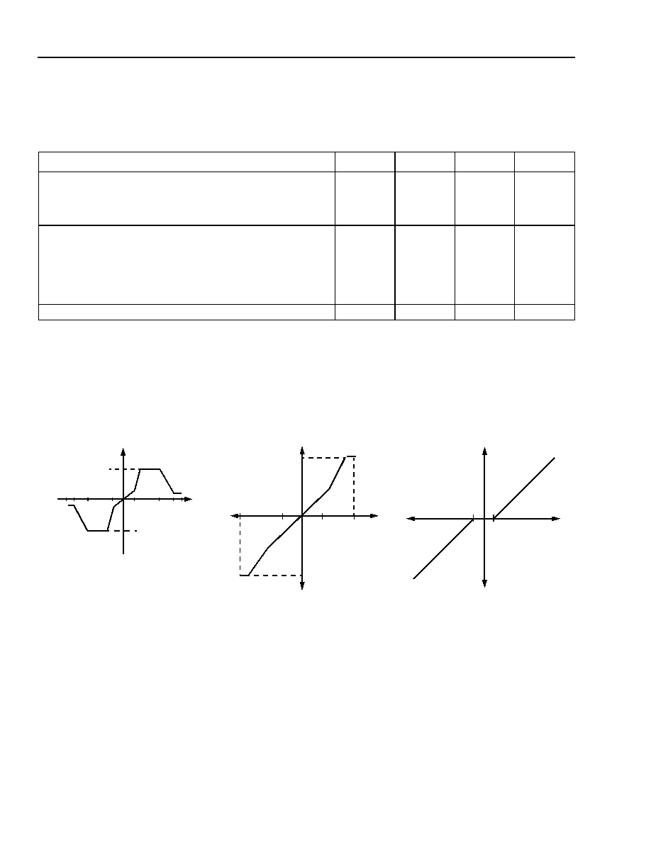
On-State Switch I-V Characteristics
Parameter Min
Typ
Max
Unit
Off State:
Maximum Differential Voltage
dc Leakage Current (Vsw = ±475 V) (pole to pole)
Isolation
--
--
--
--
--
--
±475
±20
±320
V
µA
V
On State (see On-State Switch I-V Characteristics section):
Resistance
Voltage
Steady-state Current
1
Surge Current (10 x 700
µ
s pulse)
2
Release Current
--
--
--
--
--
--
--
--
--
500
15
3
150
2
--
V
mA
A
µ
A
dV/dT Sensitivity
2, 3
--
200
--
V/µs
5-5990.c(F)
A. Line Break Switch SW1, SW2
12-3291.a(F)
B. Ring Return SW3
12-3292.a(F)
C. Ring Access SW4
Figure 4. On-State Switch I-V Characteristics
I
LIM1
I
SW
+1.5
2/3 R
ON
R
ON
≠1.5
≠I
LIM1
+V
MAX
V
SW
I
LIM2
≠I
LIM2
+V
2
+V
1
≠V
MAX
≠V
2
≠V
1
≠V
MAX
≠I
LIMIT
+I
LIMIT
+V
MAX
V
SW
+1.5 V
≠1.5 V
R
ON
2/3 R
ON
CURRENT
LIMITING
I
SW
2/3 R
ON
CURRENT
LIMITING
≠V
OS
+V
OS
V
SW
R
ON
I
SW
R
ON
Data Sheet
July 2001
Forward Battery SLIC and Ringing Relay for TR-57 Applications
L9312 Line Interface and Line Access Circuit
Agere Systems Inc.
21
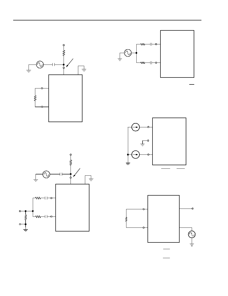
Test Configurations
12-3524f (F)
Figure 5. Basic Test Circuit
TRING
RRING
RSW
RTS
PR
PT
V
PROG
LCTH
V
REF
LCF
CF2
TXI
VTX
ITR
PWR/
V
BAT1
V
DD
D
GND
NSTAT
TRING
RING
TIP
V
REF
V
CC
50
50
R
LOOP
0.1
µ
F
0.1
µ
F
0.1
µ
F
0.1
µ
F
V
BAT2
/PWR
V
BAT1
V
CC
V
DD
NSTAT
B0
B0
B1
B1
B2
B2
LATCH
LATCH
RESET
RESET
0.1
µ
F
L9312
BASIC
TEST
CIRCUIT
RING
V
BAT2
BGND
V
CC
A
GND
6.34 k
RSW
RTS
V
PROG
LCTH
100
/
600
0.1
µ
F
0.1
µ
F
OVH
CF1
RCVP
RCVN
VITR
VITR
RCV
4.13 k
V
REF
20 k
20 k
(GAIN = 2)
46.4 k
(GAIN = 8)
Data Sheet
July 2001
Forward Battery SLIC and Ringing Relay for TR-57 Applications
L9312 Line Interface and Line Access Circuit
22
Agere Systems Inc.
Test Configurations
(continued)
PSRR = 20 log
12-2582 (F)
Figure 6. Metallic PSRR
PSRR = 20 log
12-2583 (F)
Figure 7. Longitudinal PSRR
*
ANSI
is a registered trademark of the American National Stan-
dards Institute, Inc.
ANSI
*/
IEEE
STANDARD 455-1985
12-2584 (F)
Figure 8. Longitudinal Balance
12-2585 (F)
Figure 9. Longitudinal Impedance
12-2587.g (F)
Figure 10. ac Gains
V
S
4.7 µF
100
V
BAT
OR
V
CC
DISCONNECT
V
T/R
900
V
BAT
OR V
CC
PT
PR
BASIC
TEST CIRCUIT
+
≠
CAPACITOR
BYPASS
V
S
V
T/R
----------
V
S
4.7 µF
100
V
BAT
OR
V
CC
DISCONNECT
BYPASS
56.3
V
BAT
OR V
CC
PT
PR
BASIC
TEST CIRCUIT
67.5
10 µF
10 µF
67.5
V
M
+
≠
CAPACITOR
V
S
V
M
-------
PT
PR
BASIC
TEST CIRCUIT
LONGITUDINAL BALANCE = 20 log
V
S
V
M
368
100
µ
F
100
µ
F
368
V
M
+
≠
V
S
PT
PR
BASIC
TEST CIRCUIT
+
≠
+
≠
I
LONG
I
LONG
V
PT
V
PR
Z
LONG
=
OR
V
PT
I
LONG
V
PR
I
LONG
PT
PR
BASIC
TEST CIRCUIT
600
V
T/R
+
≠
G
XMT
=
VITR
V
T/R
G
RCV
=
V
T/R
V
RCV
RCV
V
S
VITR
RCV
VITR

Data Sheet
July 2001
Forward Battery SLIC and Ringing Relay for TR-57 Applications
L9312 Line Interface and Line Access Circuit
Agere Systems Inc.
23
Applications
dc Characteristics
Power Control
Under normal device operating conditions, thermal
design must ensure that the device temperature does
not rise above the thermal shutdown. Power dissipation
is highest with higher battery voltages, with higher cur-
rent limit, and under shorter dc loop conditions. Higher
ambient temperature will reduce thermal margin.
Power control may be done in several ways, by use of
the integrated automatic battery switch and a lower-
voltage auxiliary battery or by use of a power control
resistor with single battery operation. The thermal
capability of the 44-pin PLCC package is sufficient to
allow for single battery operation without the power
control resistor when the device is used under lower-
power operating conditions.
Power Derating
Operating temperature range, maximum current limit,
maximum battery voltage, minimum dc loop length, and
protection resistors' values, number of PCB board lay-
ers, and airflow, will influence the overall thermal per-
formance. The still-air thermal resistance of the 44-pin
PLCC package is typically 38
∞
C/W for a two-layer
board with 0 LFPM airflow.
The L9312 will enter thermal shutdown at a tempera-
ture of 150
∞
C. The thermal design should ensure that
the SLIC does not reach this temperature under normal
operating conditions.
For this example, assume a maximum ambient operat-
ing temperature of 85
∞
C, a maximum current limit of
30 mA, and a maximum battery of ≠56 V. Further
assume a (worst-case) minimum dc loop of 20
for
wire resistance, 50
protection resistors, and 200
for the handset. Include the effects of parameter toler-
ance in these calculations.
T
TSD
≠ T
AMBIENT(max)
= allowed thermal rise
150
∞
C ≠ 85
∞
C = 65
∞
C
Allowed thermal rise =
package thermal impedance x SLIC power dissipation
65
∞
C = 38
∞
C/W x SLIC power dissipation
Allowed SLIC power dissipation (P
D
) = 1.71 W
Thus, in this example, if the total power dissipated on
the SLIC is less than 1.71 W, it will not enter thermal
shutdown. Total SLIC power is calculated:
Total P
D
= maximum battery x (maximum current limit)
(current limit accuracy) + SLIC quiescent power.
For the L9312, the worst-case SLIC on-hook active qui-
escent power is 100 mW. Thus,
Total off-hook power = (I
LOOP
)(1.05) x (V
BATAPPLIED
) +
SLIC quiescent power
Total off-hook power = (0.030 A)(1.05) x (52) + 100 mW
Total off-hook power = 1.864 W
The power dissipated in the SLIC is the total power dis-
sipation less the power that is dissipated in the loop.
SLIC P
D
= total power ≠ loop power
Loop off-hook power = (I
LOOP
x 1.05)
2
x (R
LOOPdcmin
+
2R
P
+ R
HANDSET
)
Loop off-hook power = {(0.030 A)(1.05)}
2
x
(20
+ 100
+ 200
)
Loop off-hook power = 317.5 mW
SLIC off-hook power = total off-hook power ≠ loop off-
hook power
SLIC off-hook power = 1.864 W ≠ 0.3175 W
SLIC off-hook power = 1.5465 W < 1.71 W
Thus, under the operating conditions of this example,
the thermal capability of the 44-pin PLCC package is
adequate to ensure that the L9312 will not be driven
into thermal shutdown and no additional power control
measures are needed. If, however, for a given set of
operating conditions, the thermal capabilities of the
package are not adequate to ensure the SLIC is driven
into thermal shutdown, then one of the power control
techniques described below should be used. Addition-
ally, even if the thermal capability of the 44-pin PLCC
package is adequate to ensure that the L9312 will not
be driven into thermal shutdown, the battery switch
technique described below can be used to reduce total
short-loop power dissipation.
Automatic Battery Switch
Use of the automatic battery switch controls power dis-
sipation by automatically switching to the lower-voltage
auxiliary battery under short dc loop conditions, thus
reducing the short-loop power that is generated. This
has the advantage of not only controlling device tem-
perature rise, but reducing overall power dissipation.
The switch will automatically apply the appropriate bat-
tery to support the dc loop. No logic control is needed
to control the switch. Switching is quiet, and the dc loop
current will not be interrupted when switching between
batteries. The lower-voltage auxiliary battery is con-
nected to the V
BAT2
/PRW package pin.
Data Sheet
July 2001
Forward Battery SLIC and Ringing Relay for TR-57 Applications
L9312 Line Interface and Line Access Circuit
24
Agere Systems Inc.
Applications
(continued)
dc Characteristics
(continued)
Automatic Battery Switch (continued)
The equation governing the switch point is as follows:
R
LOOP
=
≠ 2R
P
≠ R
dc
A graph showing loop and battery current versus loop
resistance with use of the battery switch is shown in
Figure 11.
The V
BAT2
voltage must be chosen properly so that the
power dissipation is minimized. When the voltage at
pin PR equals V
BAT2
+ 1 V + (50
x I
LOOP
), at least
98% of the loop current minus 2.5 mA flows into V
BAT2
and 2.5 mA + 2% of the loop current plus quiescent
current flows into V
BAT1
.
To choose V
BAT2
, add:
1. Maximum tip overhead voltage (2 V for V
OVH
= 0).
2. Maximum loop voltage (maximum loop resistance,
protection resistance, and dc feed resistance
[100
] times the maximum loop current limit).
3. 1 V for the soft switch.
Thus, for a 40 mA current limit, 640
loop, 30
pro-
tection resistors, and 3.17 dBm signal (V
OVH
= 0):
V
BAT2
= ≠(2 + 0.042 x (100 + 60 + 640) + 1) = ≠36.6 V
Then, for any loop resistance from 0
to 640
, the
worst-case V
BAT1
and V
BAT2
currents will be:
I
BAT1
= 1.39 mA + 2.5 mA + 0.02 x (42 mA ≠ 2.5 mA) =
4.68 mA
I
BAT2
= (0.98) x 42 mA = 38.71 mA
Total max power = 1.641 W (V
BAT
= ≠48 V)
Note that to minimize power statistically, this may not
be the best choice for V
BAT2
. Over a large number of
lines, power is minimized according to the statistical
distribution of loop resistance.
12-3470a (F)
Figure 11. L9312 Loop/Battery Current (with Battery
Switch) vs. Loop Resistance
Power Control Resistor
Device temperature rise may be controlled with use of
a single battery voltage by use of a power control resis-
tor. This technique will reduce power dissipation on the
chip, by sharing the total power not dissipated in the
loop between the L9312 and the power control resistor.
It does not, however, reduce the total power con-
sumed, as does use of the auxiliary battery. The power
control resistor is connected from the primary battery to
the V
BAT2
/PWR node of the device.
The magnitude of the power control resistor must be
low enough to ensure that sufficient power is dissipated
on the resistor to ensure the L9312 does not exceed its
thermal shutdown temperature. At the same time, the
more power that is dissipated by the power control
resistor, the higher the resistor's power rating must be,
and thus, the more costly the resistor. The following
equations are used to optimize the choice (magnitude
and power rating) of the power control resistor.
V
BAT2
3.0
≠
I
LIM
-----------------------------------
0
200
0.000
0.004
0.010
R
LOOP
(
)
400
BAT
T
E
RY
/
L
OOP
CURRENT
(m
A)
600
1000
800
0.016
I
LOOPdc
I
BAT1
I
BAT2
0.002
0.006
0.012
0.018
0.008
0.014
0.020
0.022
0.024
0.026
0.028
0.030

Data Sheet
July 2001
Forward Battery SLIC and Ringing Relay for TR-57 Applications
L9312 Line Interface and Line Access Circuit
Agere Systems Inc.
25
Applications
(continued)
dc Characteristics
(continued)
Power Control Resistor (continued)
Again assume:
T
TSD
≠ T
AMBIENT(max)
= allowed thermal rise
150
∞
C ≠ 85
∞
C = 65
∞
C
Allowed thermal rise =
package thermal impedance x SLIC power dissipation
65
∞
C = 38
∞
C/W x SLIC power dissipation
Allowed SLIC power dissipation (P
D
) = 1.71 W
This time, assume a maximum ambient operating tem-
perature of 85
∞
C, a maximum current limit of 45 mA
(including tolerance), and a maximum battery of ≠56 V.
Again, assume a (worst-case) minimum dc loop of 0
and that 50
protection resistors are used. Assume
the handset is 200
:
Total P
D
= (56 V x 45 mA) + 0.100 W
Total P
D
= 2.34 W + 0.100 W
Total P
D
= 2.4375 W
Again, the power dissipated in the SLIC is the total
power dissipation less the power that is dissipated in
the loop.
SLIC P
D
= total power ≠ loop power
Loop power = (I
LIM
)
2
x (R
LOOPdcmin
+ 2R
P
+ R
HANDSET
)
Loop power = (45 mA)
2
x (0
+ 100
+ 200
)
Loop power = 0.6075 W
SLIC power = 2.4375 W ≠ 0.6075 W
SLIC power = 1.83 W > 1.5 W
Under these extreme conditions, thermal margin is
increased via an external power control resistor.
The power dissipated in the power control resistor is
calculated by:
P
PRW
=
where in this example:
P
PRW
is power in the resistor
V
BAT
= ≠52 V
V
LOOP
= I
LIM
* (R
LOOP
+ R
PROT
)
V
ROH
is the ring-side overhead voltage of the SLIC.
Since this device is dc unbalanced, the tip side over-
head will remain typically at ≠2 V and the ring side over-
head will vary with the voltage at V
OH
. For the total tip/
ring default overhead of 5.5 V, the ring overhead is typi-
cally 3.5 V.
Overhead Voltage
Overhead is programmable in the active mode via an
applied voltage source at the device's OVH control
input. The voltage source may be an external voltage
source or derived via a resistor divider network from
the V
REF
SLIC output or an external voltage source. A
programmable external voltage source may be used to
provide software control of the overhead voltage.
The overhead voltage (V
OH
) is related to the OVH volt-
age by:
V
OH
= 5.5 V + 5 x V
OVH
(V)
Overall accuracy is determined by the accuracy of the
voltage source and the accuracy of any external resis-
tor divider network used and voltage offsets due to the
specified input bias current. If a resistor divider from
V
REF
is used, lower magnitude resistor will give a more
accurate result due to a lower offset associated with
the input bias current; however, lower value resistors
will also draw more power from V
REF
. The sum of pro-
gramming resistors should be between 75 k
and
200 k
.
Note that a default overhead voltage of 5.5 V is
achieved by shorting input pin OVH to analog ground.
Internally, the SLIC needs typically 2 V from each sup-
ply rail to bias the amplifier circuitry. This can be
thought of as an internal saturation voltage.
The default overhead provides sufficient headroom for
on-hook transmission of a 3.14 dBm signal into 900
.
3.14 = 10 log
V = 1.36 V, which is required over and above the inter-
nal saturation voltage for signal swing.
1.36 V + 4 V = 5.36 V < 5.5 V default overhead; thus, a
3.14 dBm into 900
signal is passed without clipping
distortion.
The overhead voltage accuracy achieved will not only
be affected by the accuracy of the internal SLIC cir-
cuitry, but also by the accuracy of the voltage source
and the accuracy of any external resistor divider net-
work used.
V
BAT
V
ROH
≠
V
L OOP
≠
(
)
2
R
PWR
----------------------------------------------------------------------
V
2
0.9
---------

Data Sheet
July 2001
Forward Battery SLIC and Ringing Relay for TR-57 Applications
L9312 Line Interface and Line Access Circuit
26
Agere Systems Inc.
Applications
(continued)
dc Characteristics
(continued)
dc Loop Current Limit
In the active modes, dc current limit is programmable
via an applied voltage source at the device's V
PROG
control input. The voltage source may be an external
voltage source or derived via a resistor divider network
from the V
REF
SLIC output or an external voltage
source. A programmable external voltage source may
be used to provide software control of the loop current
limit. The loop current limit (I
LIM
) is related to the V
PROG
voltage by:
I
LIM
(mA) = 50 x V
PROG
(V)
Note that the overall current-limit accuracy achieved
will not only be affected by the specified accuracy of
the internal SLIC current-limit circuit (accuracy associ-
ated with the 50 term), but also by the accuracy of the
voltage source and the accuracy of any external resis-
tor divider network used and voltage offsets due to the
specified input bias current. If a resistor divider from
V
REF
is used, a lower magnitude resistor will give a
more accurate result due to a lower offset associated
with the input bias current; however, lower value resis-
tors will also draw more power from V
REF
. The sum of
the two resistors in the resistor divider should be
between 75 k
and 200 k
. Offset at V
PROG
and V
REF
accuracies are specified in Table 6.
The above equation describes the active mode steady-
state current-limit response. There will be a transient
response of the current-limit circuit (with the device in
the active mode) upon an on- to off-hook transition.
Typical active mode transient current-limit response is
given in Table 14.
Table 14. Typical Active Mode On- to Off-Hook Tip/
Ring Current-Limit Transient Response
The current limit with the SLIC set in an active mode
will be different from the current limit with the SLIC set
in the scan mode. This is due to differences in the scan
clamp circuit versus the active tip/ring drive amplifiers.
The scan mode current limit is fixed and is a function of
the internal design of the scan clamp circuit. The
steady-state scan mode current limit will be a typical
40 mA to 50 mA and may, over temperature and pro-
cess, vary typically from 30 mA to 110 mA. The scan
clamp current limit will typically settle to its steady-state
value within 300 ms.
Loop Range
The dc loop range is calculated using:
R
L
=
≠ 2R
P
≠ R
dc
V
BAT1
is used because we are calculating the maximum
loop range. The loop resistance value where the device
automatically switches to V
BAT2
is calculated in the
Automatic Battery Switch section of this data sheet.
Battery Feed
The L9312 operates in a dc unbalanced mode. In the
forward active state, under open circuit (on-hook) con-
ditions, with the default overhead chosen, the tip to ring
voltage will be a nominal 5.5 V less than the battery.
This is the overhead voltage. The tip and ring overhead
is achieved by biasing ring a nominal 3.5 V above bat-
tery and by biasing tip a nominal 2.0 V below ground.
During off-hook conditions, some dc resistance will be
applied to the subscriber loop as a function of the phys-
ical loop length, protection, and telephone handset. As
the dc resistance decreases from infinity (on-hook) to
some finite value (off-hook), the tip to ring voltage will
decrease as shown in Figure 12.
12-3431a (F)
Figure 12. Tip/Ring Voltage
Parameter
Value
Unit
dc Loop Current:
Active Mode
R
LOOP
= 100
On- to Off-hook
Transition t < 5 ms
I
LIM
+ 60
mA
dc Loop Current:
Active Mode
R
LOOP
= 100
On- to Off-hook
Transition t < 50 ms
I
LIM
+ 20
mA
dc Loop Current:
Active Mode
R
LOOP
= 100
On- to Off-hook
Transition t < 300 ms
I
LIM
mA
V
BAT
V
OH
≠
I
L OOP
----------------------------------
VTIP TO GND
(1/2)R
dc
BEGIN CURRENT LIMITING
(1/2)R
dc
(1/2)R
dc
+ R
LIM
DECREASING LOOP LENGTH
V
BAT
VRING TO GND
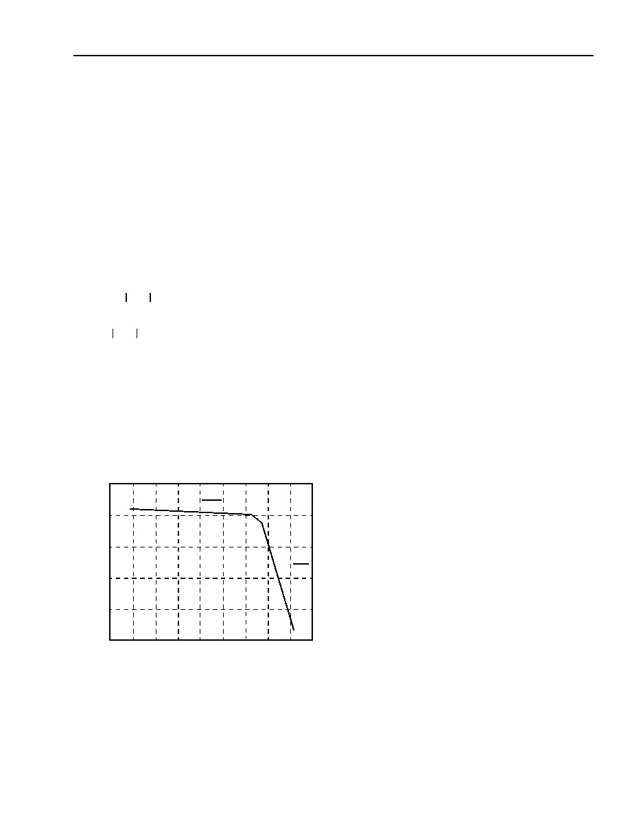
Data Sheet
July 2001
Forward Battery SLIC and Ringing Relay for TR-57 Applications
L9312 Line Interface and Line Access Circuit
Agere Systems Inc.
27
Applications
(continued)
dc Characteristics
(continued)
Battery Feed (continued)
As illustrated in Figure 12, as loop length decreases,
the tip to ground voltage will decrease with a slope cor-
responding to one-half the internal dc feed resistance
of the SLIC (typical 75
). The ring to ground voltage
will also decrease with a slope corresponding to one-
half the internal dc feed resistance of the SLIC, until the
SLIC reaches the current-limit region of operation. At
that point, the slope of the ring to ground voltage will
increase to the sum of one half the internal dc feed
resistance plus approximately 10 k
.
The dc feed characteristic can be described by:
I
LOOP
=
V
T/R
=
Where:
I
LOOP
= dc loop current.
V
T/R
= dc loop voltage.
V
BAT
= battery voltage magnitude.
V
OH
= overhead voltage.
R
LOOP
= loop resistance, including wire and handset
resistance.
R
P
= protection resistance.
R
dc
= SLIC internal dc feed resistance.
12-3050.g (F)
Notes:
V
BAT1
= ≠48 V.
V
BAT2
= ≠24 V.
I
LIM
= 40 mA (R
PROG
= 66.5 k
).
Figure 13. L9312 Loop Current vs. Loop Voltage
Refer to Figure 12 and Figure 13 in this section and to
Figure 11 in the Automatic Battery Switch section.
Starting from the on-hook condition and going through
to a short circuit, the curve passes through two regions:
Region 1: on-hook and low loop currents: the slope cor-
responds to the dc feed resistance of the SLIC (plus
any series resistance). The open-circuit voltage is the
battery voltage less the overhead voltage of the device.
Region 2: current limit: the dc current is limited to a
value determined by V
PROG
. This region of the dc tem-
plate has a high resistance (10 k
).
Notice that the I-V curve is uninterrupted when the
power is shifted from the high-voltage battery to the
low-voltage battery (if auxiliary battery option is used).
This is shown in Figure 11 in the Automatic Battery
Switch section.
Longitudinal to Metallic Balance
Longitudinal to metallic balance at PT/PR is specified in
the Electrical Characteristics section of this data sheet.
Supervision
Loop Closure
Loop closure supervision threshold is programmed via
an applied voltage source or ground, through a resistor
at the LCTH input. Loop closure status is presented at
the NSTAT output. NSTAT is an unlatched output that
represents either the loop closure or ring trip status,
depending on the device state. See Table 2 for more
details. Loop closure threshold current (I
LCTH
) is set by:
= I
LCTH
(mA)
where:
R
LCTH
is a resistor from the LCTH node to ground or a
voltage source.
V
LCTH
is ground or an external voltage source.
There is a built-in hysteresis associated with the loop
closure detector. The above equation describes the on-
hook to off-hook threshold. To help prevent false
glitches, the off-hook to on-hook threshold will be a typ-
ical 20% lower than the corresponding on-hook to off-
hook threshold.
V
BAT
V
OH
≠
R
LOOP
2R
P
R
dc
+
+
------------------------------------------------------
V
BAT
V
OH
≠
(
)
R
LOOP
∑
R
LOOP
2R
P
R
d c
+
+
----------------------------------------------------------------
L
OOP CURRE
NT
(m
A)
0
5
10
25
0
20
30
40
50
LOOP VOLTAGE (V)
15
20
10
1
R
dc
30
45
35
40
1
10 k
250 V
REF
V
LC TH
≠
(
)
R
L CT H
k
(
)
---------------------------------------------------

Data Sheet
July 2001
Forward Battery SLIC and Ringing Relay for TR-57 Applications
L9312 Line Interface and Line Access Circuit
28
Agere Systems Inc.
Supervision
(continued)
Ring Trip
Ring trip is set by the value of RS1.
The ring trip threshold at the ring trip inputs is ±2.5 V
minimum, ±3.5 V maximum.
A resistor value of 400
, as shown in Figure 4, will set
the ring trip current threshold to ±7.5 mA typical.
Ring trip is asserted upon entering the ringing mode
until the second zero crossing of ringing. This is either
a positive-going zero crossing (between ≠40 V and
≠30 V at ≠50 V V
BAT
) or a negative-going zero crossing
(between ≠10 V and ≠20 V at ≠50 V V
BAT
). The different
threshold for positive-going and negative-going zero
crossings is the result of hysteresis of approximately
20 V. The act of turning on the switch may or may not
produce a ringing zero crossing, therefore, there may
be a delay of up to almost one cycle of ringing or 50 ms
until NSTAT is high.
Ring trip will not be asserted unless the ring trip thresh-
old is exceeded for two zero crossings. This is either a
positive-going zero crossing (between ≠40 V and ≠30 V
at ≠50 V V
BAT
) or a negative-going zero crossing
(between ≠10 V and ≠20 V at ≠50 V V
BAT
). The different
threshold for positive-going and negative-going zero
crossings is the result of hysteresis of approximately
20 V.
Note that since the ringing voltage is monitored at
RSW, one zero crossing can occur at switch turn-on
depending on initial conditions.
Ring trip is asserted immediately if the ring trip input is
15 V ± 3 V.
Switching Behavior
The solid-state ring relay in the L9312 device is able to
provide either make-before-break or break-before-
make timing with respect to switching into and out of
the ring mode. If switching is done directly into and out
of the ring mode, the design of the L9312 will give
make-before-break switching with respect to both the
ring and tip side switches. To achieve break-before-
make switching, the user should via software control
enter an intermediate all-off mode when switching into
and out of the ring mode. The all-off state should be
held a minimum of 8 ms.
Make-Before-Break Operation
The break switches are constructed from DMOS tran-
sistors. The tip side ring return is also a DMOS transis-
tor. Because the on resistance of the break switches is
less than the tip side ring return switch, the break
switches are physically bigger. This implies a larger
gate to source capacitance, with inherently slower
switching speeds since it will take longer to charge or
discharge the gate to source capacitance of the break
switches (to change the state of the switch). The ring
access switch is a pnpn type device. The pnpn device
has inherently faster switching speeds than any of the
DMOS type switches.
Going from the active to ring mode, the smaller tip side
ring return switch and the pnpn ring access switch will
change states before the larger break switches. Thus,
the ring contacts are made before the line break
switches are broken: make-before-break operation.
Going from the ring mode to active or scan, the natural
tendency is for the smaller tip side ring return DMOS to
break or open, before the larger DMOS can turn on.
This would not be make-before-break operation on the
tip side. Thus, circuitry is added to speed up charging
of the tip break switch, to speed up the turn on of that
switch to give make-before-break operation on the tip
side.
On the ring side, going from the ring mode to the active
or scan mode, the pnpn will not turn off until the ring
current drops below the hold current of the pnpn device
(which is typically 500
µ
A); this is effectively zero cur-
rent for zero current turn off. This can take up to one-
half cycle of ringing to occur. With this inherent delay in
switching by the pnpn ring access switch, the break
switches will make contact before the ring access
switch breaks contact; so again, make-before-break
switching is achieved.
With the make-before-break switch, there will be a
period of time (depending on ring signal frequency but
measured in tens of microseconds) where all four
switch contacts will be on. This means that the ring
generator will be connected through the current-limited
break switches to the input of the SLIC device. Current
will be limited by the break switch current limit, and this
will not damage the SLIC. This current may, however,
cause a false glitch at the NSTAT supervision output
that will need to be digitally filtered. The board designer
should consider any ramifications of this state on the
overall system or ring generator and battery design.
The major benefit of make-before-break switching is
that it will minimize any impulse noise generated during
ringing cadence. In many cases when operating the
switch in the make-before-break mode, no special
design to switch at zero current and voltage crossing is
required. Impulse noise generation when using solid-
state relays is documented in the
Impulse Noise and
the L758X Series of Solid State Switches
Application
Note.

Data Sheet
July 2001
Forward Battery SLIC and Ringing Relay for TR-57 Applications
L9312 Line Interface and Line Access Circuit
Agere Systems Inc.
29
Supervision
(continued)
Break-Before-Make Operation
To achieve break-before-make, use the logic control
sequence device switching as shown below.
Table 15. Break-Before-Make Logic Control
Sequence Device Switching
The advantage of break-before-make operation is that
it eliminates the current spike when the ring access
relay changes state. The disadvantage is that it forces
an all-off state. Under inductive ringing loads, due to
Ldi/dt effects, it may cause a reduction in the impulse
noise performance compared to make-before-break
switching.
Protection
External Protection
An external overvoltage clamp is required to ensure
that the off-state and on-state ratings of the solid-state
break switch and solid-state ring access switch are not
exceeded. The solid-state switches in the L9312 are
constructed in a dielectrically isolated high-voltage
technology. Because of the high device-to-device isola-
tion that is inherent in the dielectric isolation, only a tip
to ground and a ring to ground clamp is required. A tip
to ring overvoltage clamp is not needed. A foldback or
crowbar type device is recommended to minimize
power across the solid-state switches under a fault
condition.
The break switches and tip return switch are con-
structed from DMOS transistors. Because the on resis-
tance of the break switches is less than the tip side ring
return switch, the break switches are physically bigger
and have a higher current handling capability. Addition-
ally, the break switches have a foldback characteristic
that enables them to survive a higher on-state voltage
(320 V) than the tip ring return switch (130 V), which
does not have the foldback characteristic. (See On-
State Switch I-V Characteristics section.) The ring
access switch is a pnpn type device. Additionally, the
ring side will see the full power ring voltage, and the tip
side switch will see the power ringing voltage that is
attenuated by the ringing load, subscriber loop, feed
resistor, and protection resistors. Because of these dif-
ferences, the protection requirements on the tip side
are different from the protection requirements on the
ring side. Thus, it is recommended that an asymmetri-
cal (with respect to tip and ring) overvoltage protection
scheme be used.
Please contact your Agere Account Representative for
a recommended protection device.
Additionally, a series protection resistor with a fusible
characteristic or a PTC resistor is recommended to
limit current during lightning and power cross faults. A
minimum 50
is recommended in tip and ring.
The overall device protection is achieved through a
combination of the external overvoltage and overcur-
rent devices, along with the integrated thermal shut-
down feature, the integrated window comparator,
the break switch foldback characteristic, and the
dc/dynamic current-limit response of the break and tip
return switches.
Active Mode Response at PT/PR
The line break switches and tip return switch are cur-
rent-limited switches. The current-limit mechanism lim-
its current through the switch to the specified dc current
limit under low frequency or dc faults (power cross
and/or tip-ring to ground short) and limits the current to
the specified dynamic current-limit response under
transient faults, such as lightning.
During a lightning fault (typical 1000 V 10 x 700
µ
s
applied surge), the current-limited line break switches
will pass typically 2.5 A for 0.5
µ
s before forcing the
break switches off. Once in the off state, the external
protection device must ensure that the off-state voltage
rating of 320 V is not exceeded. Note that the maxi-
mum differential voltage is the positive zener rating of
the protection device less the battery voltage, which
will appear on the line feed side of the switch.
State
Break
Switches
Ring
Switches
Comment
Active/Scan
closed
open
--
Disconnect
(all-off)
open
open
hold
>8 ms
Ring
open
closed
--
Disconnect
(all-off)
open
open
hold
>8 ms
Active/Scan
closed
open
--

Data Sheet
July 2001
Forward Battery SLIC and Ringing Relay for TR-57 Applications
L9312 Line Interface and Line Access Circuit
30
Agere Systems Inc.
Protection
(continued)
Active Mode Response at PT/PR
(continued)
For a lower-voltage power cross, whose maximum
peak voltage is below the foldback voltage breakpoint 1
(V1), the current-limited break switch will pass the cur-
rent equal to the dc current limit. The current limit has a
negative temperate coefficient, so as the device contin-
ues to pass current, the current limit will reduce with
increasing device temperature. Ultimately, the device
will reach the thermal shutdown temperature and the
thermal shutdown mechanism will force an all-off state,
which will stop current flow and begin device cooling. In
the all-off state, the external protection device ensures
that the switch off-state voltage rating is not exceeded.
Once the device cools significantly, the break switches
will turn on, and current will begin to flow again, until
temperature forces the all-off state. This will continue
until the fault condition is gone.
Sneak-under surge is a voltage surge that is just below
the clamping threshold of the secondary protection
device. For this type of surge, when the surge voltage
is below the foldback voltage breakpoint 1, operation is
as described above. When the surge voltage rises
above the foldback voltage breakpoint 1 (V1), but is still
less than the secondary protector clamping voltage, the
line break switch will crowbar into the high-impedance
region of its I-V characteristic and reduce current to the
specified I
LIMIT
2 value.
For surges whose magnitude range above the trigger
of the external secondary protector, the device will
operate as described above for the portion of the surge
below the secondary protector trigger voltage. When
the voltage rises above the external secondary protec-
tor's trigger voltage, the secondary protector will crow-
bar on shunting fault current to ground and reducing
the tip/ring voltage seen at the device.
In the active mode, the external secondary protector
must ensure that the off-state voltage ratings of the ring
access and ring return switch are not exceeded. Nor-
mally, the ring return switch is connected to ground on
the TRING side and to the protector on the PT side;
thus, the protector on the tip side in the active mode
must clamp at less than 320 V. As will be seen in the
Ring Mode Response at PT/PR section, during the
power ringing mode, this clamp voltage on the tip side
is significantly less than 320 V.
Normally, the ring access switch is connected to the
ring generator on the RRING side and to the protector
on the PR side; thus, on one side of the switch there is
the battery voltage and the peak negative ring signal,
and on the PR side, the maximum turn-on voltage of
the secondary protector. The ring access switch is of
pnpn construction. Thus, if the off-state voltage rating
of the ring access switch is exceeded, the device will
crowbar into a low-impedance state. This will cause a
surge into the ring generator and can cause the on-
state current rating of the switch to be exceeded.
The difference of the battery plus peak negative ring
signal voltage less the maximum turn on of the second-
ary protector must not exceed the off-state voltage rat-
ing of the ring access switch. Additionally, as the
secondary protector will see the power ring signal, the
minimum turn-on rating of the secondary protector
must be high enough to not clamp the ring signal and
cause clipping distortion. The ring side will see the full-
power ring voltage, and the tip side switch will see the
power ringing voltage that is attenuated by the ringing
load, subscriber loop, feed resistor, and protection
resistors; thus, the ring side secondary protector
requires a higher clamping voltage than the tip side.
Ring Mode Response at PT/PR
In this mode, the line break switches are off and the
ring access and ring return switch is on. The secondary
protectors must ensure that the minimum off-state volt-
age rating of the line break switches is not exceeded.
Note that the maximum differential voltage is the posi-
tive zener rating of the protection device less the bat-
tery voltage which will appear on the line feed side of
the switch.
The ring access switch is a pnpn type switch. This
switch has no internal current limiting. Thus, through
external current limit, the user must ensure that the
surge ratings (both dynamic and dc for lightning and
power cross faults) are not exceeded. A minimum
400
ring feed resistor is recommended. This resistor
also will set the ring trip threshold. See the Ring Trip
section within the Supervision section of this data sheet.
During a lightning fault (typical 1000 V 10 x 700
µ
s
applied surge), the current-limited tip return switch will
pass, typically 2.5 A for 0.5
µ
s before forcing the switch
off. Once in the off state, the external protection device
must ensure that the off-state voltage rating of 320 V is
not exceeded.

Data Sheet
July 2001
Forward Battery SLIC and Ringing Relay for TR-57 Applications
L9312 Line Interface and Line Access Circuit
Agere Systems Inc.
31
Protection
(continued)
Ring Mode Response at PT/PR
(continued)
For power cross for lower-voltage faults, the ring return
switch will behave like the line break switches. How-
ever, tip return switch does not have the foldback
clamping feature that is included in the line break
switches; thus, in the on state, the voltage seen by the
ring return switch before damage is less than the line
break switches. The on-state voltage of the line break
switches can go up to the off-state voltage rating. The
ring return voltage should see less than 130 V in the on
state. Thus, the secondary protector on the ring side
should have a maximum crowbar voltage of 130 V.
With typical protection device tolerance, this implies a
minimum clamping voltage of 100 V. The users should
ensure, based on minimum loop length, ringing load,
and peak ring signal voltage, that the ring signal is not
distorted by the (lower) voltage rating of the tip-side
protector.
Internal Tertiary Protection
The external secondary protector and switch current
limit protect the 320 V high-voltage switches from light-
ning and power cross conditions. Integrated into the
LILAC IC is an internal tertiary protection scheme that
is meant to protect the 90 V SLIC portion of the device
from residue fault current and voltages that may be
passed through the switches to the actual SLIC inputs.
This scheme includes an internal diode bridge voltage
clamp and a battery out of range detector that forces
an all-off condition if the battery voltage falls high or low
out of the specified operating range.
Diode Bridge
The internal inputs of the actual SLIC chip are clamped
to ground and to V
BAT1
by an integrated diode bridge.
Residual positive fault currents are clamped to ground
and residual negative fault currents are clamped to bat-
tery. This implies that the battery have some current
sinking capability.
High common-mode currents, as may be seen under a
fault condition, will be sensed and reduced to zero by
the battery monitor circuit (see Battery Out of Range
Detector: High [Magnitude] section). However, this
detector will not prevent longitudinal current from flow-
ing into battery. The battery supply must have the abil-
ity to sink longitudinal currents as specified in the
longitudinal current capability requirement in Table 6.
Battery Out of Range Detector: High (Magnitude)
This feature is useful in remote power applications
where a dc-dc converter with limited ability to sink cur-
rent is used as the primary battery supply. Under a fault
condition, the diode bridge will want to sink current into
the battery. As a function of the dc-dc converter input
capacitance and design, this current may cause the
magnitude of supply voltage to rise and ultimately
cause damage to the supply. To prevent damage to the
supply, the LILAC device will monitor the battery supply
voltage. If the magnitude of the battery rises above the
maximum specified operating battery, the battery out of
range detector will force the line break switches and
ring access switches into an all-off state, and will also
force the SLIC into the disconnect state. This will stop
the current flow into the battery, preventing damage to
the battery fault conditions. NSTAT is forced low during
this mode of operation.
Battery Out of Range Detector: Low (Magnitude)
The LILAC device will monitor the battery supply volt-
age. If the magnitude of the battery drops below the
minimum specified operating battery, the battery out of
range detector will force the line break switches and
ring access switches into an all-off state, and will also
force the SLIC into the disconnect state. NSTAT is
forced low during this mode of operation.

Data Sheet
July 2001
Forward Battery SLIC and Ringing Relay for TR-57 Applications
L9312 Line Interface and Line Access Circuit
32
Agere Systems Inc.
ac Applications
ac Parameters
There are four key ac design parameters. Termination
impedance is the impedance looking into the 2-wire
port of the line card. It is set to match the impedance of
the telephone loop in order to minimize echo return to
the telephone set. Transmit gain is measured from the
2-wire port to the PCM highway, while receive gain is
done from the PCM highway to the transmit port.
Transmit and receive gains may be specified in terms
of an actual gain, or in terms of a transmission level
point (TLP), that is, the actual ac transmission level in
dBm. Finally, the hybrid balance network cancels the
unwanted amount of the receive signal that appears at
the transmit port.
Codec Types
At this point in the design, the codec needs to be
selected. The interface network between the SLIC and
codec can then be designed. Below is a brief codec
feature summary.
First-Generation Codecs. These perform the basic
filtering, A/D (transmit), D/A (receive), and
µ
-law/A-law
companding. They all have an op amp in front of the
A/D converter for transmit gain setting and hybrid bal-
ance (cancellation at the summing node). Depending
on the type, some have differential analog input stages,
differential analog output stages, +5 V only or
±
5 V
operation, and
µ
-law/A-law selectability. These are
available in single and quad designs. This type of
codec requires continuous time analog filtering via
external resistor/capacitor networks to set the ac
design parameters. An example of this type of codec is
the Agere T7504 quad 5 V only codec.
This type of codec tends to be the most economical in
terms of piece part price, but tends to require more
external components than a third-generation codec.
Further ac parameters are fixed by the external R/C
network so software control of ac parameters is diffi-
cult.
Third-Generation Codecs. This class of devices
includes all ac parameters set digitally under micropro-
cessor control. Depending on the device, it may or may
not have data control latches. Additional functionality
sometimes offered includes tone plant generation and
reception, PPM generation, test algorithms, and echo
cancellation. Again, this type of codec may be +5 V
only or
±
5 V operation, single quad or 16-channel, and
µ
-law/A-law or 16-bit linear coding selectable. Exam-
ples of this type of codec are the Agere T8536/7 (5 V
only, quad, standard features), T8533/4 (5 V only, quad
with echo cancellation), and the T8531/36 (5 V only,
16-channel with self-test).
ac Interface Network
The ac interface network between the L9312 and the
codec will vary depending on the codec selected. With
a first-generation codec, the interface between the
L9312 and codec actually sets the ac parameters. With
a third-generation codec, all ac parameters are set dig-
itally, internal to the codec; thus, the interface between
the L9312 and this type of codec is designed to avoid
overload at the codec input in the transmit direction,
and to optimize signal to noise ratio (S/N) in the receive
direction.
Because the design requirements are very different
with a first- or third-generation codec, the L9312 is
offered with two different receive gains. Each receive
gain was chosen to optimize, in terms of external com-
ponents required, the ac interface between the L9312
and codec.

Data Sheet
July 2001
Forward Battery SLIC and Ringing Relay for TR-57 Applications
L9312 Line Interface and Line Access Circuit
Agere Systems Inc.
33
ac Applications
(continued)
ac Interface Network
(continued)
With a first-generation codec, the termination imped-
ance is set by providing gain shaping through a feed-
back network from the SLIC VITR output to the SLIC
RCVN/RCVP inputs. The L9312 provides a transcon-
ductance from T/R to VITR in the transmit direction and
a single ended to differential gain in the receive direc-
tion, from either RCVN or RCVP to T/R. Assuming a
short from VITR to RCVN or RCVP, the maximum
impedance that is seen looking into the SLIC is the
product of the SLIC transconductance times the SLIC
receive gain, plus the protection resistors. The various
specified termination impedance can range over the
voiceband as low as 300
up to over 1000
. Thus, if
the SLIC gains are too low, it will be impossible to syn-
thesize the higher termination impedances. Further, the
termination that is achieved will be far less than what is
calculated by assuming a short for SLIC output to SLIC
input. In the receive direction, in order to control echo,
the gain is typically a loss, which requires a loss net-
work at the SLIC RCVN/RCVP inputs, which will
reduce the amount of gain that is available for termina-
tion impedance. For this reason, a high-gain SLIC is
required with a first-generation codec.
With a third-generation codec, the line card designer
has different concerns. To design the ac interface, the
designer must first decide upon all termination imped-
ance, hybrid balances, and TLP requirements that the
line card must meet. In the transmit direction, the only
concern is that the SLIC does not provide a signal that
is too large and overloads the codec input. Thus, for
the highest TLP that is being designed to, given the
SLIC gain, the designer, as a function of voiceband fre-
quency, must ensure the codec is not overloaded. With
a given TLP and a given SLIC gain, if the signal will
cause a codec overload, the designer must insert some
sort of loss, typically a resistor divider, between the
SLIC output and codec input.
In the receive direction, the issue is to optimize the
S/N. Again, the designer must consider all the consid-
ered TLPs. The idea, for all desired TLPs, is to run the
codec at or as close as possible to its maximum output
signal, to optimize the S/N. Remember, noise floor is
constant, so the larger the signal from the codec, the
better the S/N. The problem is if the codec is feeding a
high-gain SLIC, either an external resistor divider is
needed to knock the gain down to meet the TLP
requirements, or the codec is not operated near maxi-
mum signal levels, thus compromising the S/N.
Thus, it appears the solution is to have a SLIC with a
low gain, especially in the receive direction. This will
allow the codec to operate near its maximum output
signal (to optimize S/N), without an external resistor
divider (to minimize cost).
Note also that some third-generation codecs require
the designer to provide an inherent resistive termina-
tion via external networks. The codec will then provide
gain shaping, as a function of frequency, to meet the
return loss requirements. Further stability issues may
add external components or excessive ground plane
requirements to the design.
To meet the unique requirements of both types of
codecs, the L9312 offers two receive gain choices.
These receive gains are mask programmable at the
factory and are offered as two different code variations.
For interface with a first-generation codec, the L9312 is
offered with a receive gain of 8. For interface with a
third-generation codec, the L9312 is offered with a
receive gain of 2. In either case, the transconductance
in the transmit direction, or the transmit gain, is 300
.
This selection of receive gain gives the designer the
flexibility to maximize performance and minimize exter-
nal components, regardless of the type of codec cho-
sen.
Design Tools
The following examples illustrate the design tech-
niques/equations followed to design the ac interface
with a first- or third-generation codec for both a resis-
tive and complex design. To aid the line circuit design,
Agere has available
Windows
*-based spreadsheets to
do the individual component calculations. Further,
Agere has available
PSPICE
models for circuit simula-
tion and verification. Consult your Agere Account Rep-
resentative to obtain these design tools.
First-Generation Codec ac Interface Network
Termination impedance may be specified as purely
resistive or complex, that is, some combination of
resistors and capacitors that causes the impedance to
vary with frequency. The design for a pure resistive ter-
mination, such as 600
, does not vary with frequency,
so it is somewhat more straightforward than a complex
termination design. For this reason, the case of a resis-
tive design and complex design will be shown sepa-
rately.
*
Windows
is a registered trademark of Microsoft Corporation.
PSPICE
is a registered trademark of MicroSim Corporation.
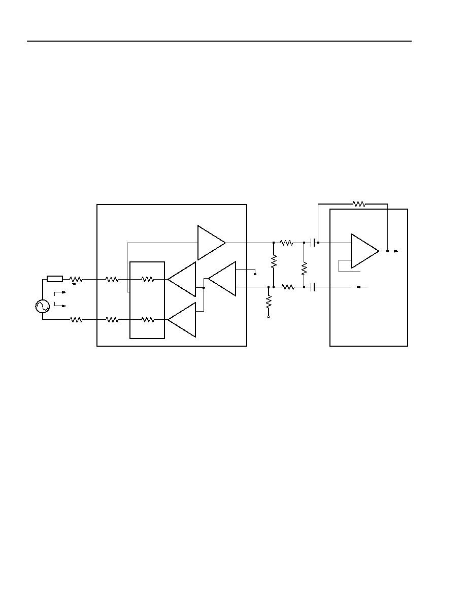
34
Data Sheet
July 2001
Forward Battery SLIC and Ringing Relay for TR-57 Applications
L9312 Line Interface and Line Access Circuit
34
Agere Systems Inc.
ac Applications
(continued)
First-Generation Codec ac Interface Net-
work: Resistive Termination
The following reference circuit shows the complete
SLIC schematic for interface to the Agere T7504 first-
generation codec for a resistive termination imped-
ance. For this example, the ac interface was designed
for a 600
resistive termination and hybrid balance
with transmit gain and receive gain set to 0 dBm.
Also, this example illustrates the device with a single
battery operation, fixed current limit, and fixed loop clo-
sure threshold. This is a lower feature application
example.
Resistor R
GN
is optional. It compensates for any mis-
match of input bias voltage at the RCVN/RCVP inputs.
If it is not used, there may be a slight offset at tip and
ring due to mismatch of input bias voltage at the
RCVN/RCVP inputs. It is very common to simply tie
RCVN directly to ground in this particular mode of oper-
ation. If used, to calculate R
GN
, the impedance from
RCVN to ac ground should equal the impedance from
RCVP to ac ground.
12-3580 (F)
Figure 14. ac Equivalent Circuit
R
P
Z
T
+
≠
R
P
V
T/R
I
T/R
V
S
Z
T/R
+
≠
RING
A
V
= ≠1
A
V
= 1
VITR
CURRENT
SENSE
TIP
+
≠
R
T3
R
RCV
R
HB1
R
T6
RCVN
RCVP
R
X
VGSX
VF
X
IN
VFR
1/4 T7504 CODEC
R
GP
2.4 V
≠0.300 V/mA
A
V
= 4
L9312
VF
X
IP
18
18
20
20
BREAK
SWITCH
BREAK
SWITCH
V
REF
V
REF

Data Sheet
July 2001
Forward Battery SLIC and Ringing Relay for TR-57 Applications
L9312 Line Interface and Line Access Circuit
Agere Systems Inc.
35
ac Applications
(continued)
First-Generation Codec ac Interface Network: Resistive Termination
(continued)
Example 1, Real Termination
The following design equations refer to the circuit in Figure 14. Use these to synthesize real termination imped-
ance.
Termination Impedance:
Z
T
=
Receive Gain:
Transmit Gain:
Hybrid Balance:
h
bal
= 20 log
h
bal
= 20 log
To optimize the hybrid balance, the sum of the currents at the VFX input of the codec op amp should be set to 0.
The expression for ZHB becomes:
V
T/R
I
T/R
≠
------------
Z
T
76
2
+
R
P
2400
1
R
T 3
R
G P
---------
R
T3
R
R C V
------------
+
+
-----------------------------------
+
=
g
rcv
V
T/R
V
FR
------------
=
g
rcv
8
1
R
R C V
R
T 3
-----------
R
R C V
R
G P
------------
+
+
1
Z
T
Z
T/R
---------
+
------------------------------------------------------------------
=
g
t x
V
GSX
V
T/R
-----------
=
g
t x
R
X
≠
R
T 6
---------
300
Z
T/R
---------
◊
=
R
X
R
H B1
---------------
g
t x
≠
g
rcv
◊
V
GSX
V
FR
---------------
R
H B
k
( )
R
X
g
t x
g
rcv
◊
-------------------
=
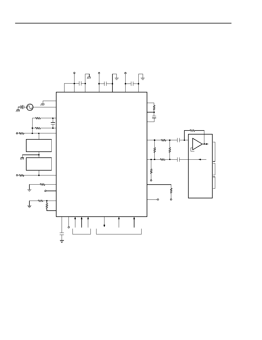
Data Sheet
July 2001
Forward Battery SLIC and Ringing Relay for TR-57 Applications
L9312 Line Interface and Line Access Circuit
36
Agere Systems Inc.
ac Applications
(continued)
First-Generation Codec ac Interface Network: Resistive Termination
(continued)
Example 1, Real Termination (continued)
12-3521h (F)
Notes:
Termination impedance = 600
.
Hybrid balance = 600
.
Tx = 0 dBm.
Rx = 0 dBm.
Figure 15. Agere T7504 First-Generation Codec Resistive Termination, Single Battery Operation
R
G1
FUSIBLE
50
C
VBAT1
0.1
µ
F
V
BAT1
RCVN
RTS
L9312
V
BAT
C
F2
0.015
µ
F
LCF
VTX
RCVP
R
T3
140 k
R
RCV
100 k
R
HB1
100 k
VFXIN
R
X
100 k
GSX
V
FRO
DX
DR
FSE
FSEP
MCLK
ASEL
1/4 T7504
CODEC
CONTROL
INPUTS
PCM
HIGHWAY
SYNC
AND
CLOCK
≠
+
ITR
C
RTI
0.1
µ
F
AGND
V
DD
+2.4 V
C
C2
0.1
µ
F
R
GN
R
GP
43.2 k
1 M
50
R
RING
T
RING
100 V--130 V
SECONDARY
OR PTC
FUSIBLE
OR PTC
R
RTF
400
RINGING
SOURCE
C
CC
0.1
µ
F
V
CC
C
DD
0.1
µ
F
V
DD
A
D
C
TX
0.15
µ
F
R
GX
6.34 k
C
C1
0.33
µ
F
R
T6
49.9 k
RSW
PT
PWR
V
BAT2
/
V
CC
BGND
V
BAT1
DGND
TXI
VITR
PROTECTOR
180 V--330 V
SECONDARY
PROTECTOR
B2
B1
B0
CF2
MULTIPLEXED
DATA BUS
TO/FROM
MICROPROCESSOR
PER-LINE
TO/FROM
MICROPROCESSOR
PR
(GAIN OF 8)
NSTAT
RESET
LATCH
28.3 k
LCTH (10 mA)
V
PROG
(I
LIMIT
= 25 mA)
V
REF
R
VPROG
23.2 k
R
VREF
86.7 k
R
LCTH
59 k
OVH (5.5 V
OH
)
V
PROG
(I
LIMIT
= 25 mA)
V
REF
V
REF
CF1

Data Sheet
July 2001
Forward Battery SLIC and Ringing Relay for TR-57 Applications
L9312 Line Interface and Line Access Circuit
Agere Systems Inc.
37
ac Applications
(continued)
First-Generation Codec ac Interface Network: Resistive Termination
(continued)
Example 1, Real Termination (continued)
Table 16. L9312 Parts List for Agere T7504 First-Generation Codec Resistive Termination, Single Battery
Operation
* See your Agere Account Representative for a recommended secondary protection device.
Name
Value
Tolerance
Rating
Function
Fault Protection
R
PR
50
1%
Fusible
or PTC
Protection resistor.
R
PT
50
1%
Fusible
or PTC
Protection resistor.
Protector*
180 V to 320 V
--
--
Ring-side secondary protector.
Protector*
100 V to 130 V
--
--
Tip-side secondary protector.
Power Supply
C
BAT1
0.1
µ
F
20%
100 V
Filter capacitor.
C
CC
0.1
µ
F
20%
10 V
Filter capacitor.
C
DD
0.1
µ
F
20% 10
V
Filter
capacitor.
C
F2
0.015
µ
F
20%
100 V
Filter capacitor.
dc Profile
R
VPROG
23.2 k
1%
1/16 W
With R
VREF
fix dc current limit.
R
VREF
86.7 k
1%
1/16 W
With R
VPROG
fix dc current limit.
Supervision
C
RTF
0.1
µ
F
20%
100 V
Ring trip filter capacitor.
R
RTF
1 M
1%
1/16 W
Ring trip filter resistor.
R
RS1
400
5%
2 W
Sets ring trip threshold.
R
LCTH
59 k
1%
1/16 W
With R
VREF
, fix loop supervision threshold.
ac Interface
R
GX
6.34 k
1%
1/16 W
Sets T/R to VITR transconductance.
C
TX
0.15
µ
F
20% 10
V
ac/dc
separation.
C
C1
0.33
µ
F
20%
10 V
dc blocking capacitor.
C
C2
0.1
µ
F
20%
10 V
dc blocking capacitor.
R
T3
140 k
1%
1/16 W
With R
GP
and R
RCV
, sets termination impedance and
receive gain.
R
T6
49.9 k
1%
1/16 W
With R
X
, sets transmit gain.
R
X
100 k
1% 1/16
W
With
R
T6
, sets transmit gain.
R
HB
100 k
1%
1/16 W
With R
X
, sets hybrid balance.
R
RCV
100 k
1%
1/16 W
With R
GP
and R
T3
, sets termination impedance and
receive gain.
R
GP
43.2 k
1%
1/16 W
With R
RCV
and R
T3
, sets termination impedance and
receive gain.
R
GN
Optional
28.3 k
1%
1/16 W
Optional. Compensates for input offset at RCVN/RCVP.
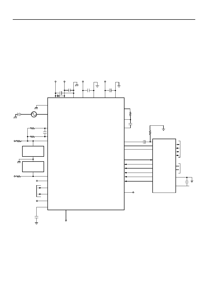
Data Sheet
July 2001
Forward Battery SLIC and Ringing Relay for TR-57 Applications
L9312 Line Interface and Line Access Circuit
38
Agere Systems Inc.
ac Applications
(continued)
Third-Generation Codec ac Interface Network: Complex Termination
The following reference circuit shows the complete SLIC schematic for interface to the Agere T8536 third-genera-
tion. All ac parameters are programmed by the T8536. Note that this codec differentiates itself in that no external
components are required in the ac interface to provide a dc termination impedance or for stability. Also, this exam-
ple illustrates the device using the battery switch with multiple battery operation, programmable current limit, and
programmable loop closure threshold. Please see the T8535/6 data sheet for information on coefficient program-
ming.
12-3527i (F)
Figure 16. L9312 for Agere T8536 Third-Generation Codec, Dual Battery Operation, ac and dc Parameters,
Fully Programmable
R
S1
FUSIBLE
50
C
VBAT1
0.1
µ
F
V
BAT1
RCVN
RTS
V
PROG
(I
LIMIT
= 25 mA)
LCTH (THRESHOLD = 11 mA)
V
BAT
C
F2
0.015
µ
F
VTX
RCVP
VFROP
VFXIN
VFRON
DX0
DR1
FS
BCLK
DGND
V
DD
PCM
HIGHWAY
SYNC
AND
CLOCK
ITR
C
RTS
0.1
µ
F
AGND
V
DD
1 M
50
R
RING
100 V--130 V
SECONDARY
OR PTC
FUSIBLE
OR PTC
R
RTF
400
RINGING
SOURCE
C
CC
0.1
µ
F
V
CC
C
DD
0.1
µ
F
V
DD
A
D
C
TX
0.15
µ
F
R
GX
6.34 k
C
C1
RSW
PT
V
BAT2
/
V
CC
BGND
V
BAT1
DGND
TXI
VITR
PROTECTOR
180 V--330 V
SECONDARY
PROTECTOR
V
REF
CF2
V
BAT2
C
VBAT2
0.1
µ
F
FROM
PROGRAMMABLE
VOLTAGE
SOURCE
PWR
T
RING
LATCH
RESET
SLIC1a
SLIC0a
SLIC5a
NSTAT
B1
B2
SLIC4a
SLIC3a
B0
SLIC2a
DR0
DX1
T8536
CV
DD
0.1
µ
F
V
DD
L9312
(GAIN OF 2)
LCF
PR
0.33
µ
F
OVH
CF1
R
CIN
20 M

Data Sheet
July 2001
Forward Battery SLIC and Ringing Relay for TR-57 Applications
L9312 Line Interface and Line Access Circuit
Agere Systems Inc.
39
ac Applications
(continued)
Third-Generation Codec ac Interface Network: Complex Termination
(continued)
Table 17. L9312 Parts List for Agere T8536 Third-Generation Codec, Dual Battery Operation, ac and dc
Parameters, Fully Programmable
* See your Agere Account Representative for a recommended secondary protection device.
Name
Value
Tolerance
Rating
Function
Fault Protection
R
PR
50
1%
Fusible or
PTC
Protection resistor.
R
PT
50
1%
Fusible or
PTC
Protection resistor.
Protector*
180 V to 320 V
--
--
Ring-side secondary protector.
Protector*
100 V to 130 V
--
--
Tip-side secondary protector.
Power Supply
Diode
1N4004
--
--
Reverse battery current.
C
BAT1
0.1
µ
F
20%
100 V
Filter capacitor.
C
BAT2
0.1
µ
F
20%
50 V
Filter capacitor.
C
CC
0.1
µ
F
20%
10 V
Filter capacitor.
C
DD
0.1
µ
F
20%
10 V
Filter capacitor.
C
F2
0.015
µ
F
20%
100 V
Filter capacitor.
Supervision
C
RTF
0.1
µ
F
20%
100 V
Ring trip filter capacitor.
R
RTF
1 M
1%
1/16 W
Ring trip filter resistor.
R
RS1
400
5%
2 W
Sets ring trip threshold.
ac Interface
R
GX
6.34 k
1%
1/16 W
Sets T/R to VITR transconductance.
R
CIN
20 M
5%
1/16 W
dc bias.
C
TX
0.15
µ
F
20%
10 V
ac/dc separation.
C
C1
0.33
µ
F
20%
10 V
dc blocking capacitor.
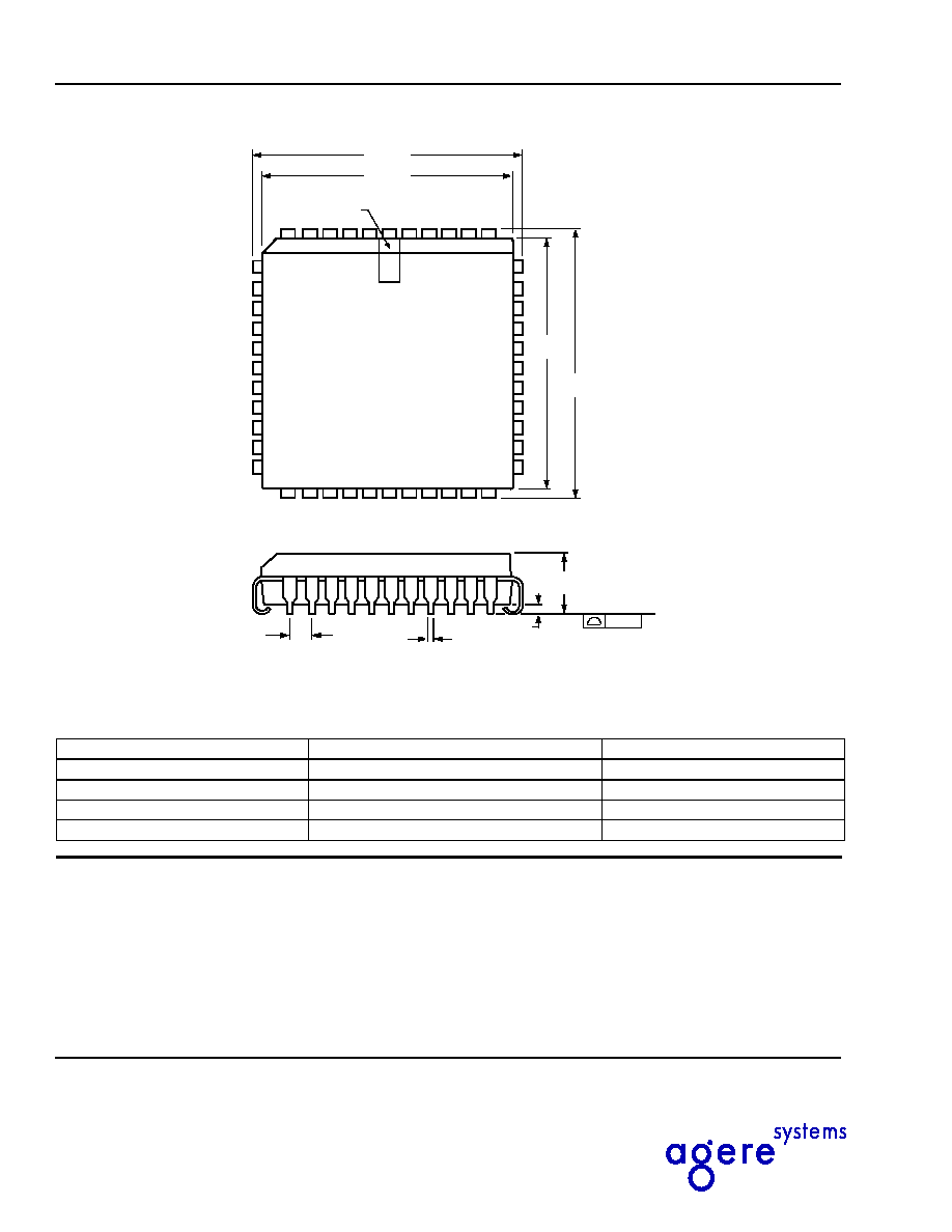
Data Sheet
July 2001
Forward Battery SLIC and Ringing Relay for TR-57 Applications
L9312 Line Interface and Line Access Circuit
Agere Systems Inc. reserves the right to make changes to the product(s) or information contained herein without notice. No liability is assumed as a result of their use or application.
Copyright © 2001 Agere Systems Inc.
All Rights Reserved
July 2001
DS01-192ALC (Replaces DS01-170ALC)
For additional information, contact your Agere Systems Account Manager or the following:
INTERNET: http://www.agere.com
E-MAIL: docmaster@micro.lucent.com
N. AMERICA:
Agere Systems Inc., 555 Union Boulevard, Room 30L-15P-BA, Allentown, PA 18109-3286
1-800-372-2447, FAX 610-712-4106 (In CANADA: 1-800-553-2448, FAX 610-712-4106)
ASIA PACIFIC: Agere Systems Singapore Pte. Ltd., 77 Science Park Drive, #03-18 Cintech III, Singapore 118256
Tel. (65) 778 8833, FAX (65) 777 7495
CHINA: Agere Systems (Shanghai) Co., Ltd., 33/F Jin Mao Tower, 88 Century Boulevard Pudong, Shanghai 200121 PRC
Tel. (86) 21 50471212, FAX (86) 21 50472266
JAPAN: Agere Systems Japan Ltd., 7-18, Higashi-Gotanda 2-chome, Shinagawa-ku, Tokyo 141, Japan
Tel. (81) 3 5421 1600, FAX (81) 3 5421 1700
EUROPE: Data Requests: DATALINE: Tel. (44) 7000 582 368, FAX (44) 1189 328 148
Technical Inquiries: GERMANY: (49) 89 95086 0 (Munich), UNITED KINGDOM: (44) 1344 865 900 (Ascot),
FRANCE: (33) 1 40 83 68 00 (Paris), SWEDEN: (46) 8 594 607 00 (Stockholm), FINLAND: (358) 9 3507670 (Helsinki),
ITALY: (39) 02 6608131 (Milan), SPAIN: (34) 1 807 1441 (Madrid)
Outline Diagram
5-2506F
Ordering Information
Device Part Number Package Comcode
LUCL9312AP-D 44-Pin PLCC, Dry-bagged 108698127
LUCL9312AP-DT 44-Pin PLCC, Dry-bagged, Tape and Reel 108698135
LUCL9312GP-D 44-Pin PLCC, Dry-bagged 108698200
LUCL9312GP-DT 44-Pin PLCC, Dry-bagged, Tape and Reel 108698218
4.57
MAX
1.27 TYP
0.53
MAX
0.10
SEATING PLANE
0.51 MIN
TYP
1
6
40
7
17 29
39
18 28
PIN #1 IDENTIFIER
ZONE
16.66 MAX
17.65 MAX
16.66
MAX
17.65
MAX