Data Sheet
April 20, 2004
LCK4310
Low-Voltage PLL Clock Driver
1 Features
s
Output operating frequencies up to 1.25 GHz max.
s
100 ps part≠to≠part skew.
s
40 ps typical output≠to≠output skew.
s
Cycle-to-cycle jitter 5 ps max.
s
3.3 V and 2.5 V compatible.
s
Internal input pulldown resistors.
s
Q output will default low with inputs open or at V
EE
.
s
Meets or exceeds Joint Electron Device Engineering
Council (JEDEC) specification EIA
Æ
/JESD78 IC latchup
test.
s
Moisture sensitivity level 1.
s
Flammability rating: UL
Æ
≠94 code V≠0 at 1/8 in., oxygen
index 28 to 34.
s
Pin-for-pin compatible with ON Semiconductor
Æ
part
number MC100LVE310.
2 Description
The LCK4310 is a low-voltage, low-skew 2:8 differential
emitter-coupled logic (ECL) fanout buffer designed with
clock distribution in mind. The device features fully
differential clock paths to minimize both device and system
skew. The LCK4310 offers two selectable clock inputs to
allow for redundant or test clocks to be incorporated into
the system clock trees.
To ensure that the tight skew specification is met, it is
necessary that both sides of the differential output are
terminated into 50
, even if only one side is being used. In
most applications, all eight differential pairs will be used
and therefore terminated. In the case where fewer than
eight pairs are used and in order to maintain minimum
skew, it is necessary to terminate at least the output pairs
adjacent to the output pair being used. Failure to follow this
guideline will result in small degradations of propagation
delay (on the order of 10 ps--20 ps) of the outputs being
used. While not catastrophic to most designs, this will result
in an increase in skew.
Note: The package corners isolate outputs from one anoth-
er such that the guideline expressed above holds only
for outputs on the same side of the package.
The LCK4310, as with most ECL devices, can be operated
from a positive voltage supply (V
DD
) in LVPECL mode. This
allows the LCK4310 to be used for high-performance clock
distribution in 3.3 V/2.5 V systems. Designers can take
advantage of the LCK4310's performance to distribute low-
skew clocks across the backplane or the board. In a PECL
environment (series or Thevenin), line terminations are
typically used since they require no additional power
supplies. If parallel termination is desired, a terminating
voltage of V
DD ≠
2.0 V will need to be provided.
An internally generated voltage supply (V
BB
pin) is
available to this device only. For single-ended input
conditions, the unused differential input is connected to
V
BB
as a switching reference voltage. V
BB
may also rebias
ac coupled inputs. When used, decouple V
BB
and V
DD
via a
0.01 µF capacitor and limit current sourcing or sinking to
0.5 mA. When not used, V
BB
should be left open.

LCK4310
Data Sheet
Low-Voltage PLL Clock Driver
April 20, 2004
2
2
Agere Systems Inc.
3 Pin Information
3.1 Pin Diagram
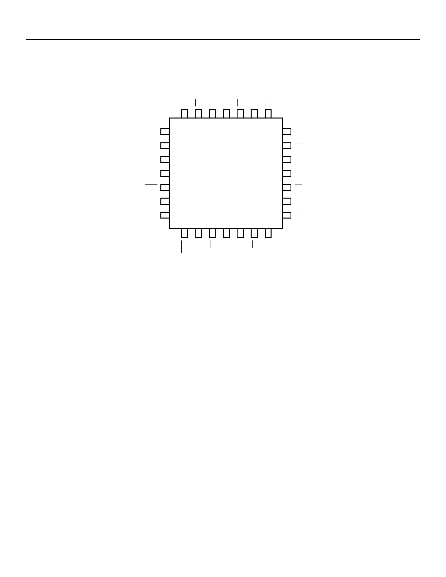
Figure 3-1. 28-Pin PLCC
WARNING: All V
DD
, V
DDO
, and V
EE
pins must be externally connected to a power supply to guarantee proper oper-
ation.
26
27
28
1
2
3
4
V
EE
CLK_SEL
CLKa
V
DD
CLKa
V
BB
CL
Kb
Q3
Q3
Q4
V
DDO
Q4
Q5
Q5
Q0
Q0
Q1
V
DDO
Q1
Q2
Q2
NC
Q7
V
DDO
Q7
Q6
Q6
18
17
16
15
14
13
12
19
20
21
22
23
24
25
11
10
9
8
7
6
5
CLKb

Data Sheet
LCK4310
April 20, 2004
Low-Voltage PLL Clock Driver
Agere Systems Inc.
3
3.2 Pin Descriptions
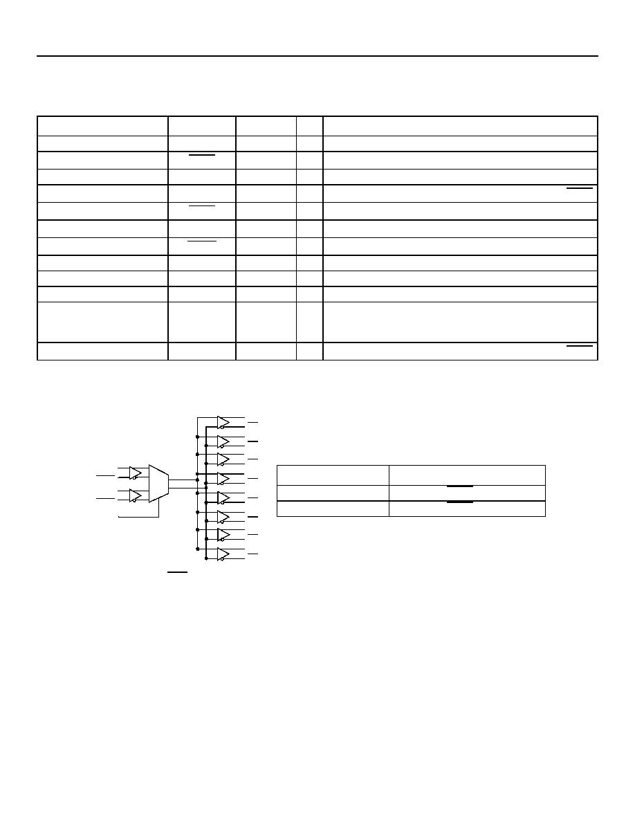
Table 3-1. Pin Descriptions
3.3 Logic Symbol
Figure 3-2. Logic Symbol
Pin
Symbol
Type
I/O
Description
1
V
DD
Power
-- Positive Power Supply.
2
CLKa
PECL
I
ECL Differential Input Clock. Makes input pair with CLKa.
3
V
BB
V
REFOUT
O Reference Voltage Output.
4
CLKb
PECL
I
ECL Differential Input Clock. Makes input pair with CLKb.
5
CLKb
PECL
I
ECL Differential Input Clock. Makes input pair with CLKb.
6
NC
--
-- No Connect.
7, 10, 12, 14, 17, 19, 21, 24
Q[7:0]
PECL
O ECL Differential Outputs.
8, 15, 22
V
DDO
Power
-- Positive Power Supply.
9, 11, 13, 16, 18, 20, 23, 25
Q[7:0]
PECL
O ECL Differential Outputs.
26
V
EE
Power
-- Negative Power Supply.
27
CLK_SEL
LVTTL
I
ECL Input Clock Select.
0 = CLKa selected.
1 = CLKb selected.
28
CLKa
PECL
I
ECL Differential Input Clock. Makes input pair with CLKa.
Q0
Q0
Q1
Q1
Q2
Q2
Q3
Q3
V
BB
Q4
Q4
Q5
Q5
Q6
Q6
Q7
Q7
CLKa
CLKa
CLKb
CLKb
CLK_SEL
CLK_SEL
Input Clock
L
CLKa/CLKa Selected
H
CLKb/CLKb Selected

LCK4310
Data Sheet
Low-Voltage PLL Clock Driver
April 20, 2004
4
4
Agere Systems Inc.
4 Absolute Maximum Ratings
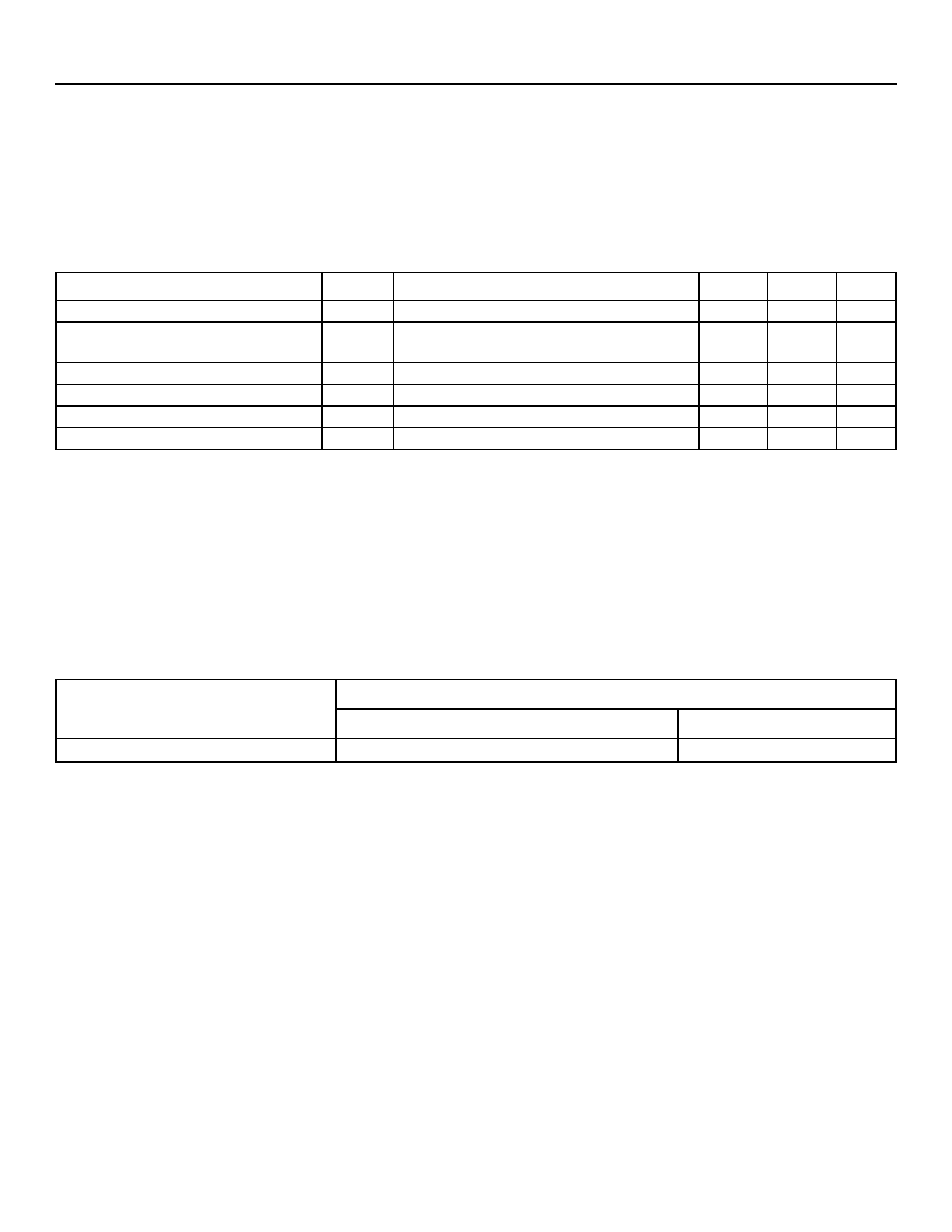
Stresses which exceed the absolute maximum ratings can cause permanent damage to the device. These are absolute
stress ratings only. Functional operation of the device is not implied at these or any other conditions in excess of those
given in the operational sections of the data sheet. Exposure to absolute maximum ratings for extended periods of time can
adversely affect device reliability.
Table 4-1. Absolute Maximum Ratings
4.1 Handling Precautions
Although electrostatic discharge (ESD) protection circuitry has been designed into this device, proper precautions must be
taken to avoid exposure to ESD and electrical overstress (EOS) during all handling, assembly, and test operations. Agere
employs both a human-body model (HBM) and a charged-device model (CDM) qualification requirement in order to
determine ESD-susceptibility limits and protection design evaluation. ESD voltage thresholds are dependent on the circuit
parameters used in each of the models, as defined by JEDEC's JESD22-A114 (HBM) and JESD22-C101 (CDM)
standards.
Table 4-2. ESD Tolerance
Parameter
Symbol
Conditions
Min
Max
Unit
PECL Mode Positive Power Supply
V
DD
V
EE
= 0 V
0
5
V
Input Voltage:
PECL Mode Positive Input Voltage
V
I
V
EE
= 0 V, V
I
V
DD
0
5
V
Output Current
I
OUT
Continuous surge
50
100
mA
V
BB
Sink/Source
I
BB
--
≠0.5
0.5
mA
Storage Temperature Range
T
stg
--
≠65
150
∞C
Wave Solder
T
SOL
<2 s to 3 s at 248 ∞C
--
265
∞C
Device
Minimum Threshold
HBM
CDM
LCK4310
>2,000 V
>1,000 V

Data Sheet
LCK4310
April 20, 2004
Low-Voltage PLL Clock Driver
Agere Systems Inc.
5
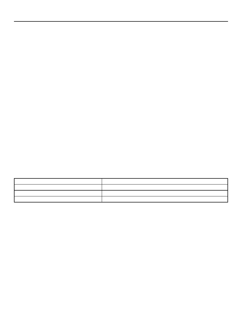
4.2 Thermal Parameters (Definitions and Values)
System and circuit board level performance depends not only on device electrical characteristics, but also on device thermal
characteristics. The thermal characteristics frequently determine the limits of circuit board or system performance, and they
can be a major cost adder or cost avoidance factor. When the die temperature is kept below 125 ∞C, temperature activated
failure mechanisms are minimized. The thermal parameters that Agere provides for its packages help the chip and system
designer choose the best package for their applications, including allowing the system designer to thermally design and in-
tegrate their systems.
It should be noted that all the parameters listed below are affected, to varying degrees, by package design (including paddle
size) and choice of materials, the amount of copper in the test board or system board, and system airflow.
JA
- Junction to Air Thermal Resistance
JA
is a number used to express the thermal performance of a part under JEDEC standard natural convection conditions.
JA
is calculated using the following formula:
JA
= (T
J
≠ T
amb
) / P; where P = power
JMA
- Junction to Moving Air Thermal Resistance
JMA
is effectively identical to
JA
but represents performance of a part mounted on a JEDEC four layer board inside a wind
tunnel with forced air convection.
JMA
is reported at airflows of 200 LFPM and 500 LFPM (linear feet per minute), which
roughly correspond to 1 m/s and 2.5 m/s (respectively).
JMA
is calculated using the following formula:
JMA
= (T
J
≠ T
amb
) / P
JC
- Junction to Case Thermal Resistance
JC
is the thermal resistance from junction to the top of the case. This number is determined by forcing nearly 100% of the
heat generated in the die out the top of the package by lowering the top case temperature. This is done by placing the top
of the package in contact with a copper slug kept at room temperature using a liquid refrigeration unit.
JC
is calculated using
the following formula:
JC
= (T
J
≠ T
C
) / P
Table 4-3. Thermal Parameter Values
Parameter
Temperature ∞C/Watt
JA
63.5
JMA
(500 lf/m)
43.5
JC
27.3

LCK4310
Data Sheet
Low-Voltage PLL Clock Driver
April 20, 2004
6
6
Agere Systems Inc.
5 Electrical Characteristics
5.1 dc Characteristics
Table 5-1. LVPECL 3.3 V dc Characteristics
V
DD
= 3.3 V, V
EE
= 0 V. Input and output parameters vary 1:1 with V
DD
. V
EE
can vary ±0.3 V. Devices are designed to meet
the dc specifications shown in this table, after thermal equilibrium has been established.
Parameter
Symbol
≠40 ∞C
25 ∞C
85 ∞C
Unit
Min
Typ
Max
Min
Typ
Max
Min
Typ
Max
Power Supply Current
I
EE
--
55
60
--
55
60
--
65
70
mA
Output High Voltage
*
* Outputs are terminated through a 50
resistor to V
DD
≠ 2 V.
V
OH
2.215
2.295
2.420
2.275
2.345
2.420
2.275
2.345
2.420
V
Output Low Voltage
*
V
OL
1.470
1.605
1.745
1.490
1.595
1.680
1.490
1.595
1.680
V
Input High Voltage (sin-
gle-ended)
V
IH
2.135
--
2.420
2.135
--
2.420
2.135
--
2.420
V
Input Low Voltage (sin-
gle-ended)
V
IL
1.490
--
1.825
1.490
--
1.825
1.490
--
1.825
V
Output Voltage
Reference
V
BB
1.92
--
2.06
1.92
--
2.06
1.92
--
2.06
V
Input High Voltage
Common-mode
Range (differential)
V
IHCMR
minimum varies 1:1 with V
EE
, maximum varies 1:1 with V
DD
. V
IHCMR
is defined as the range within which the V
IH
level may vary, with the
device still meeting the propagation delay specification. The V
IL
level must be such that the peak-to-peak voltage is less than 1.0 V and greater than or
equal to V
p-pmin
.
V
IHCMR
1.8
--
2.9
1.8
--
2.9
1.8
--
2.9
V
Input High Current
I
IH
--
--
150
--
--
150
--
--
150
µA
Input Low Current
I
IL
0.5
--
--
0.5
--
--
0.5
--
--
µA

Data Sheet
LCK4310
April 20, 2004
Low-Voltage PLL Clock Driver
Agere Systems Inc.
7
Table 5-2. LVPECL 2.5 V dc Characteristics
V
DD
= 2.5 V, V
EE
= 0 V. Input and output parameters vary 1:1 with V
DD
. V
EE
can vary ±0.3 V. Devices are designed to meet
the dc specifications shown in this table, after thermal equilibrium has been established.
Parameter
Symbol
≠40 ∞C
25 ∞C
85 ∞C
Unit
Min
Typ
Max
Min
Typ
Max
Min
Typ
Max
Power Supply Current
I
EE
--
55
60
--
55
60
--
65
70
mA
Output High Voltage
*
* Outputs are terminated through a 50
resistor to V
DD
≠ 2 V.
V
OH
1.425
1.495
1.620
1.425
1.507
1.620
1.425
1.520
1.620
V
Output Low Voltage
*
V
OL
0.730
0.790
0.955
0.730
0.820
0.955
0.730
0.825
0.955
V
Input High Voltage
(single-ended)
V
IH
2.000
--
2.400
2.000
--
2.400
2.000
--
2.400
V
Input Low Voltage
(single-ended)
V
IL
0.400
--
1.030
0.400
--
1.030
0.400
--
1.030
V
Output Voltage
Reference
V
BB
1.019
--
1.361
1.019
--
1.361
1.019
--
1.361
V
Input High Voltage
Common-mode
Range (differential)
V
IHCMR
minimum varies 1:1 with V
EE
, maximum varies 1:1 with V
DD
. V
IHCMR
is defined as the range within which the V
IH
level may vary, with the
device still meeting the propagation delay specification. The V
IL
level must be such that the peak-to-peak voltage is less than 1.0 V and greater than or
equal to V
p-pmin
.
V
IHCMR
1.0
--
2.1
1.0
--
2.1
1.0
--
2.1
V
Input High Current
I
IH
--
--
150
--
--
150
--
--
150
µA
Input Low Current
I
IL
0.5
--
--
0.5
--
--
0.5
--
--
µA

LCK4310
Data Sheet
Low-Voltage PLL Clock Driver
April 20, 2004
8
8
Agere Systems Inc.
5.2 ac Characteristics
V
DD
= 3.3/2.5 V, V
EE
= 0 V, or V
DD
= 0 V, V
EE
= ≠3.3/2.5 V. V
EE
can vary ±0.3 V.
Table 5-3. ac Characteristics
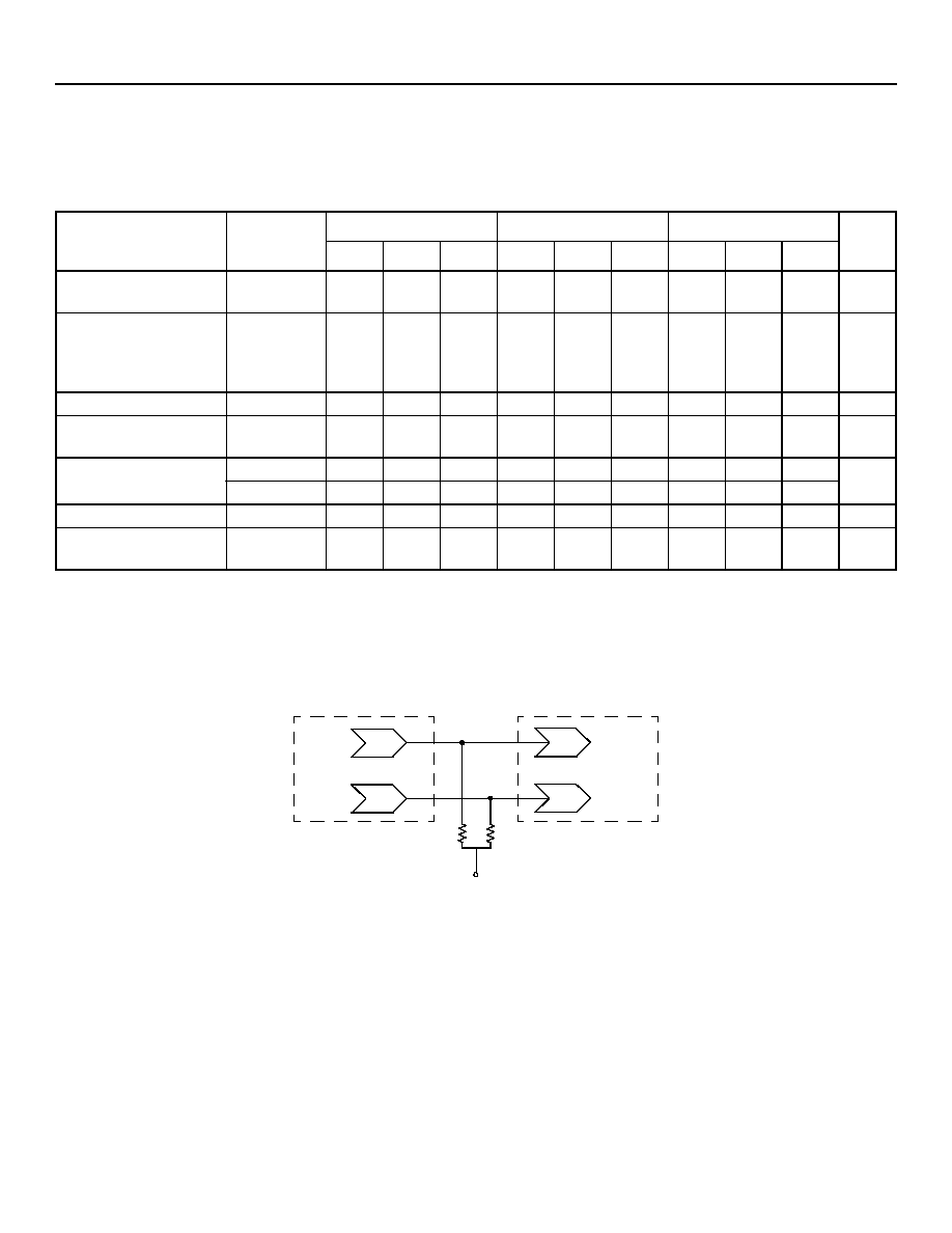
Figure 5-1. Typical Termination for Output Driver and Device Evaluation
Parameter
Symbol
≠40 ∞C
25 ∞C
85 ∞C
Unit
Min
Typ
Max
Min
Typ
Max
Min
Typ
Max
Maximum Toggle
Frequency
f
MAX
--
--
1.25
--
--
1.25
--
--
1.25
GHz
Propagation Delay to
Output:
In (differential)
*
In (single-ended)
* The differential propagation delay is defined as the delay from the crossing points of the differential input signals to the crossing point of the differential
output signals.
The single-ended propagation delay is defined as the delay from the 50% point of the input signal to the 50% point of the output signal.
t
PLH
t
PHL
525
500
--
--
725
750
550
550
--
--
750
800
575
600
--
--
775
850
ps
Within Device Skew
The within device skew is defined as the worst case difference between any two similar delay paths within a single device.
t
SKEW
--
--
40
--
--
40
--
--
40
ps
Part-to-part Skew
(differential)
t
SKEW
--
--
100
--
--
100
--
--
100
ps
Jitter
JIT
cyc-cyc
--
--
5
--
--
5
--
--
5
ps
JIT
p-p
--
--
7
--
--
7
--
--
7
Input Swing
ß
ß V
p-pmin
is defined as the minimum input differential voltage which will cause no increase in the propagation delay. The V
p-pmin
is ac limited for the
LCK4310 as a differential input as low as 50 mV will still produce full ECL levels at the output.
V
p-p
0.500
--
1
0.500
--
1
0.500
--
1
V
Output Rise/Fall Time
(20%--80%)
t
r
/t
f
200
--
600
200
--
600
200
--
600
ps
V
EE
Q
Qb
DEVICE
DRIVER
D
Db
DEVICE
RECEIVER
V
EE
= V
DD
≠ 2.0 V
50
50

Data Sheet
LCK4310
April 20, 2004
Low-Voltage PLL Clock Driver
Agere Systems Inc.
9
6 Outline Diagrams
Dimensions are in millimeters.
5-2608 (F)
1.27 TYP
0.330/0.533
0.10
SEATING PLANE
0.51 MIN
TYP
4.572
MAX
12
18
11
5
4
1
26
25
19
12.446
±
0.127
PIN #1 IDENTIFIER
ZONE
11.506
±
0.076
11.506
±
0.076
12.446
±
0.127

Copyright © 2004 Agere Systems Inc.
All Rights Reserved
April 20, 2004
DS04-169LCK (Replaces DS03-158LCK)
Agere Systems Inc. reserves the right to make changes to the product(s) or information contained herein without notice. No liability is assumed as a result of their use or application.
Agere is a registered trademark of Agere Systems Inc. Agere Systems and the Agere logo are trademarks of Agere Systems Inc.
For additional information, contact your Agere Systems Account Manager or the following:
INTERNET:
http://www.agere.com
E-MAIL:
docmaster@agere.com
N. AMERICA: Agere Systems Inc., Lehigh Valley Central Campus, Room 10A-301C, 1110 American Parkway NE, Allentown, PA 18109-9138
1-800-372-2447, FAX 610-712-4106 (In CANADA: 1-800-553-2448, FAX 610-712-4106)
ASIA:
Agere Systems Hong Kong Ltd., Suites 3201 & 3210-12, 32/F, Tower 2, The Gateway, Harbour City, Kowloon
Tel. (852) 3129-2000, FAX (852) 3129-2020
CHINA: (86) 21-54614688 (Shanghai), (86) 755-25881122 (Shenzhen)
JAPAN: (81) 3-5421-1600 (Tokyo), KOREA: (82) 2-767-1850 (Seoul), SINGAPORE: (65) 6778-8833, TAIWAN: (886) 2-2725-5858 (Taipei)
EUROPE:
Tel. (44) 1344 296 400
LCK4310
Data Sheet
Low-Voltage PLL Clock Driver
April 20, 2004
7 Ordering Information
EIA is a registered trademark of Electronic Industries Association.
UL is a registered trademark of Underwriters Laboratories, Inc.
ON Semiconductor is a registered trademark of Semiconductor Components Industries, L.L.C.
Table 7-1. Ordering Information
Device
Part Number
Pin Count
Package
Type
Comcode
LCK4310
LCK4310GF-DB
28
PLCC
Reel
700020216
LCK4310GF-DT
28
PLCC Tape
700020217

