 | –≠–Ľ–Ķ–ļ—ā—Ä–ĺ–Ĺ–Ĺ—č–Ļ –ļ–ĺ–ľ–Ņ–ĺ–Ĺ–Ķ–Ĺ—ā: LCK4953 | –°–ļ–į—á–į—ā—Ć:  PDF PDF  ZIP ZIP |
Data Sheet
November 2001
LCK4953
Low-Voltage PLL Clock Driver
Features
∑
Fully integrated PLL
∑
Output frequency up to 130 MHz in PLL mode
∑
Nine outputs with high-impedance disable
∑
32-lead TQFP
∑
50 ps cycle-to-cycle jitter
∑
Pin compatible with the Motorola
ģ
MPC953 clock
driver
Description
The LCK4953 is a PLL-based clock driver device
intended for high-performance clock tree designs.
The LCK4953 is 3.3 V compatible with output
frequencies of up to 130 MHz and output skews of
75 ps. The LCK4953 can meet the most demanding
timing requirements and employs on-chip voltage
regulators to minimize cycle-to-cycle jitter and phase
jitter.
The LCK4953 is ideal for use as a zero delay, low
skew, fan-out buffer due to its differential LVPECL
reference input along with an external feedback
input. The MROEB pin of the LCK4953, when driven
high, will reset the internal counters and 3-state the
output buffers. The LCK4953 has been optimized for
zero delay performance.
The LCK4953 is fully 3.3 V compatible and requires
no external loop filter components. All control inputs
accept LVCMOS or LVTTL compatible levels while
the outputs provide LVCMOS levels with the ability to
drive terminated 50
transmission lines. For series-
terminated 50
lines, each of the LCK4953 outputs
can drive two traces giving the device an effective
fan-out of 1:18. For the optimum combination of
board density and performance, the device is
packaged in a 7 mm
◊
7 mm 32-lead TQFP package.
Table 1. Function Table
BYPASSB
Function
1
0
PLL Enabled
PLL Bypass
MROEB
Function
1
0
Outputs Disabled
Outputs Enabled
VCOSEL
Function
1
0
ų
8
ų
4
PLLEN
Function
1
0
Select VCO
Select PELCLK
2
Agere Systems Inc.
Data Sheet
November 2001
Low-Voltage PLL Clock Driver
LCK4953
Description
(continued)
5-8653(F)
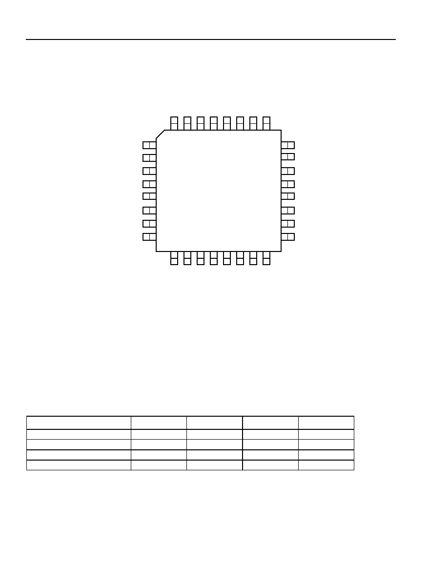
Figure 1. 32-Lead Pinout (Top View)
Absolute Maximum Ratings
Stresses which exceed the absolute maximum ratings can cause permanent damage to the device. These are
absolute stress ratings only. Functional operation of the device is not implied at these or any other conditions in
excess of those given in the operational sections of the data sheet. Exposure to absolute maximum ratings for
extended periods of time can adversely affect device reliability.
Table 2. Absolute Maximum Ratings
Parameter
Symbol
Min
Max
Unit
Supply Voltage
V
DD
≠0.3
4.2
V
Input Voltage
V
IN
≠0.3
V
DD
+ 0.3
V
Input Current
I
IN
--
Ī
20
mA
Storage Temperature Range
T
stg
≠40
125
į
C
LCK4953
1
2
3
4
5
6
7
8
24
23
22
21
20
19
18
17
16
15
14
13
12
11
10
9
25
26
27
28
29
30
31
32
V
DD
A
FBCLK
NC1
NC2
NC3
NC4
V
SS
A
PECLCKP
V
SS
Q0
V
DD
QF
B
V
SS
PLLE
N
BY
PA
SS
B
VC
O
S
EL
Q1
V
DD
Q2
V
SS
Q3
V
DD
Q4
V
SS
Q5
V
DD
Q6
V
SS
Q7
V
DD
MRO
E
B
P
E
CLCK
N
Agere Systems Inc.
3
Data Sheet
November 2001
Low-Voltage PLL Clock Driver
LCK4953
Absolute Maximum Ratings
(continued)
Table 3. dc Characteristics (T
A
= 0
į
C to 70
į
C, V
DD
= 3.3 V
Ī
5%)
Table 4. PLL Input Reference Characteristics (T
A
= 0
į
C to 70
į
C)
Table 5. ac Characteristics (T
A
= 0
į
C to 70
į
C, V
DD
= 3.3 V
Ī
5%)
Parameter
Symbol
Min
Typ
Max
Unit
Condition
Input High-voltage LVCMOS
Inputs
V
IH
2.0
--
3.6
V
--
Input Low-voltage LVCMOS
Inputs
V
IL
--
--
0.8
V
--
Peak-to-peak Input Voltage
PECL_CLK
Vp-p 300
--
1000
mV
--
Common-mode Range
PECL_CLK
V
CMR
V
DD
≠ 1.5
--
V
DD
≠ 0.6
mV
--
*
*
V
CMR
is the difference from the most positive side of the differential input signal. Normal operation is obtained when the high input is within
the V
CMR
range and the input swing lies within the Vp-p specification.
Output High Voltage
V
OH
2.4
--
--
V
I
OH
= ≠30 mA
The LCK4953 outputs can drive series- or parallel-terminated 50
(or 50
to V
CC
/2) transmission lines on the incident edge.
Output Low Voltage
V
OL
--
--
0.6
V
I
OL
= 30 mA
Input Current
I
IN
--
--
Ī
120
Ķ
A
--
Input Capacitance
C
IN
--
--
4
pF
--
Power Dissipation Capacitance
Cpd
--
12
--
pF
Per output
Maximum Quiescent Supply
Current Non-PLL
I
DDQ
--
--
1
mA
All V
DD
pins except
V
DD
A
Total Power = (I
DDPLL
+ I
DDQ
+ fCV) * V; where f = fref, V = V
DDD
, C = total load capacitance on all outputs.
Maximum PLL Supply Current
I
DDPLL
--
--
45
mA
V
DD
A pin only
Parameter
Symbol
Min
Max
Unit
Condition
Reference Input Frequency
fref
25
130
MHz
--
Reference Input Duty Cycle
trefdc
25
75
%
--
Parameter
Symbol
Min
Typ
Max
Unit
Condition
Output Rise/Fall Time
tr, tf
0.10
--
1.0
ns
0.8 V to 2.0 V
Output Duty Cycle
tpw
47
50
53
%
--
Output-to-output Skews
tsk(O)
--
--
75
ps
--
PLL V
CO
Lock Range
fV
CO
200
--
520
MHz
--
Frequency Output:
Frequency PLL
Bypass Mode
fout
25
50
--
--
--
--
65
130
250
MHz
MHz
MHz
VCOSEL = 1
VCOSEL = 0
--
Input to Ext_FB Delay (with PLL locked)
tpd (lock)
≠75
--
125
ps
tref = 75 MHz
Input to Q Delay
tpd(bypass)
3
--
7
ns
PLL bypassed
Part to Part Delay
1.5
Output Disable Time
tPLZHZ
--
--
7
ns
--
Output Enable Time
tPZL
--
--
6
ns
--
Cycle-to-cycle Jitter (peak-to-peak)
tjitter
--
--
50
ps
fout > 75 MHz
4
Agere Systems Inc.
Data Sheet
November 2001
Low-Voltage PLL Clock Driver
LCK4953
Electrical Characteristics
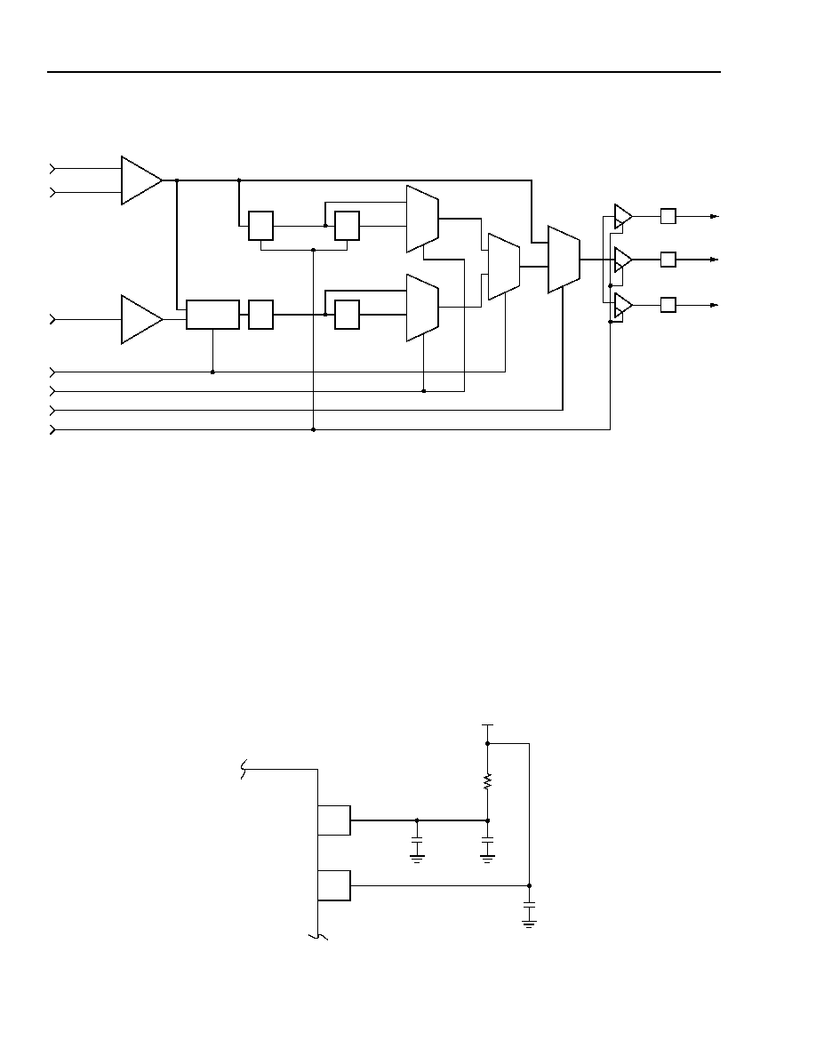
5-8654.a (F)
Figure 2. Logic Diagram
Power Supply Filtering
The LCK4953 is a mixed-signal product which is susceptible to random noise, especially when this noise is on the
power supply pins. To isolate the output buffer switching from the internal phase-locked loop, the LCK4953
provides separate power supplies for the phase-locked loop (V
DD
A) and for the output buffers (V
DD
). In a digital
system environment, besides this isolation technique, it is highly recommended that both V
DDA
and V
DD
power
supplies be filtered to reduce the random noise as much as possible.
Figure 3 illustrates a typical power supply filter scheme. A filter for the LCK4953 should be designed to target noise
in the 100 kHz to 10 MHz range, due to its susceptibility to noise with spectral content in this range. The RC filter in
Figure 3 will provide a broadband filter with approximately ≠40 dB attenuation for noise with spectral content above
20 kHz. More elaborate power supply schemes may be used to achieve increased power supply noise filtering.
5-9575(F)
Figure 3. Power Supply Filter
PECLCKP
PECLCKN
P
N
FBCLK
PLL CORE
A
Z
/4
A
Z
/4
DIVBY4
A
Z
/2
A
Z
/2
DIVBY2
DIVBY4
DIVBY2
D0
D1
SD
Z
D0
D1
SD
Z
D0
D1
SD
Z
D0
D1
SD
Z
Z
PAD
Z
PAD
Z
PAD
QFB
Q[0:6]
Q7
QFB
Q[0:6]
Q7
PLLEN
VCOSEL
BYPASSB
MROEN
0.01
Ķ
F
22
Ķ
F
R
S =
5
--10
V
DD
V
DDA
LCK4953
0.01
Ķ
F
3.3 V
Agere Systems Inc.
5
Data Sheet
November 2001
Low-Voltage PLL Clock Driver
LCK4953
Electrical Characteristics
(continued)
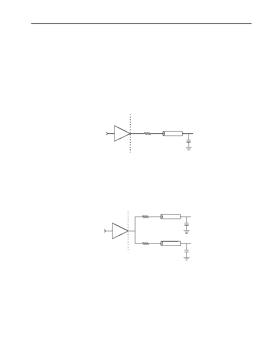
Driving Transmission Lines
The LCK4953 clock driver was designed to drive high-speed clock terminals in a terminated transmission line
environment. Point-to-point distribution of signals is a common method in most high-performance clock networks.
Either series-terminated or parallel-terminated transmission lines can be used in a point-to-point scheme. The
parallel technique terminates the signal at the end of a line with a 50
resistance to V
DD
/2. This draws a fairly high
level of dc current. Due to this aspect, only a single terminated line can be driven by each output of the LCK4953
clock driver. For the series-terminated case, however, there is no dc current draw; in turn, the outputs are capable
of driving multiple series-terminated lines.
Figure 4 illustrates an output driving a single series-terminated line.
5-9576(F)
Figure 4. Single Transmission Line
In Figure 4, because the output buffer has an impedance of 14
, the series resistance (R
s
) is set at 36
.
This
ensures that the total impedance is matched with the 50
transmission line.
Figure 5 illustrates an output driving two series-terminated lines.
5-9577(F)
Figure 5. Dual Transmission Lines
In Figure 5, the two series resistors (R
s)
are set at 22
because the 14
output buffer can be viewed as two 28
resistors in parallel. Accordingly, for each transmission line, the impedance is well matched.
OUTPUT
OUTPUT
14
BUFFER
R
S
= 36
Z
O
= 50
CLOCK
OUTPUT
OUTPUT
14
BUFFER
R
S
= 22
Z
O
= 50
CLOCK
R
S
= 22
Z
O
= 50
Motorola is a registerd trademark of Motorola, Inc.
Copyright © 2001 Agere Systems Inc.
All Rights Reserved
November 2001
DS02-034HSI (Replaces DS01-159ANET)
Agere Systems Inc. reserves the right to make changes to the product(s) or information contained herein without notice. No liability is assumed as a result of their use or application.
For additional information, contact your Agere Systems Account Manager or the following:
INTERNET:
http://www.agere.com
E-MAIL:
docmaster@agere.com
N. AMERICA:
Agere Systems Inc., 555 Union Boulevard, Room 30L-15P-BA, Allentown, PA 18109-3286
1-800-372-2447, FAX 610-712-4106 (In CANADA: 1-800-553-2448, FAX 610-712-4106)
ASIA:
Agere Systems Hong Kong Ltd., Suites 3201 & 3210-12, 32/F, Tower 2, The Gateway, Harbour City, Kowloon
Tel. (852) 3129-2000, FAX (852) 3129-2020
CHINA: (86) 21-5047-1212 (Shanghai), (86) 10-6522-5566 (Beijing), (86) 755-695-7224 (Shenzhen)
JAPAN: (81) 3-5421-1600 (Tokyo), KOREA: (82) 2-767-1850 (Seoul), SINGAPORE: (65) 778-8833, TAIWAN: (886) 2-2725-5858 (Taipei)
EUROPE:
Tel. (44) 7000 624624, FAX (44) 1344 488 045
Data Sheet
November 2001
Low-Voltage PLL Clock Driver
LCK4953
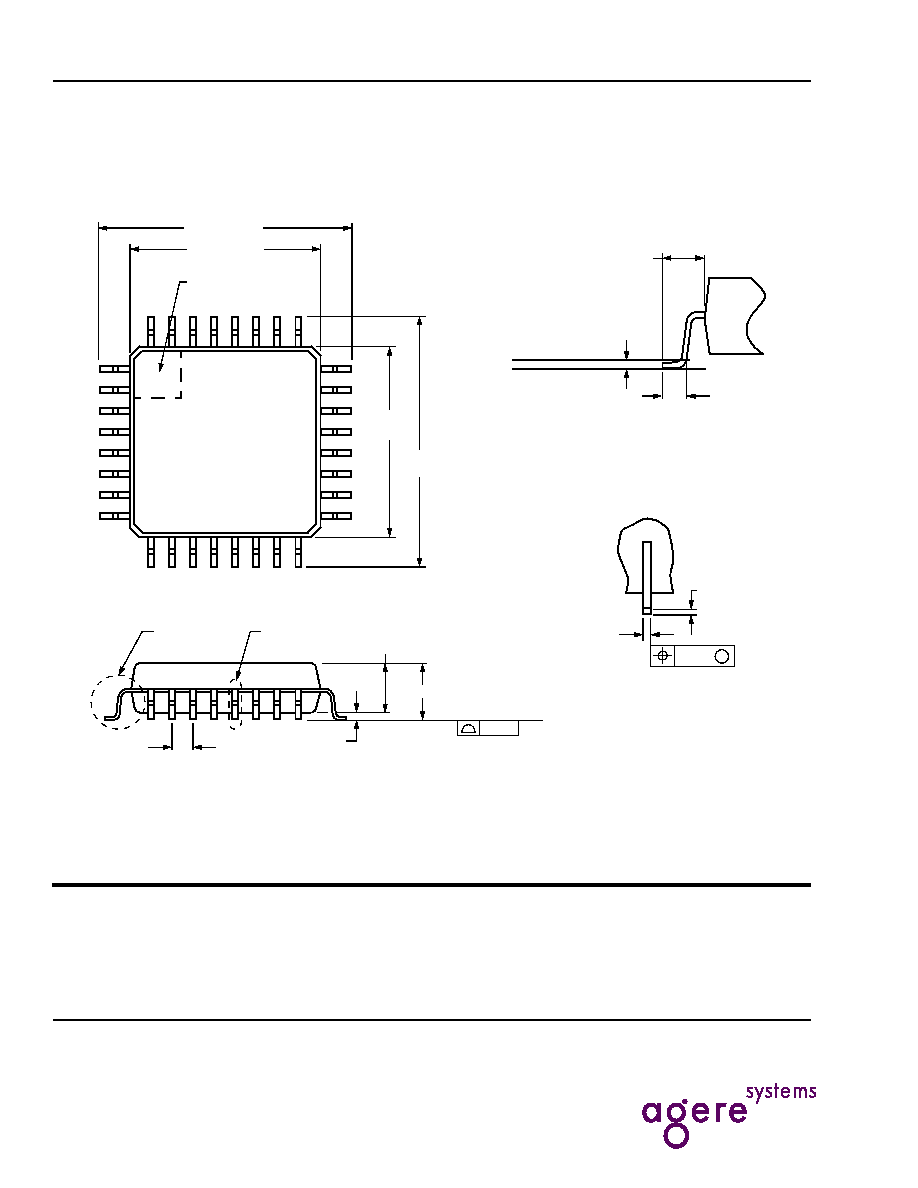
Outline Diagram
32-Pin TQFP
Dimensions are in millimeters.
12-3076(F)
PIN #1
IDENTIFIER ZONE
16
7.00 Ī 0.20
9.00 Ī 0.20
1
32
25
8
9
24
17
9.00
Ī 0.20
7.00
Ī 0.20
1.60 MAX
SEATING PLANE
DETAIL A
0.10
1.40 Ī 0.05
0.80 TYP
0.05/0.15
DETAIL B
DETAIL B
0.30/0.45
0.20
M
0.09/0.200
DETAIL A
0.45/0.75
GAGE PLANE
SEATING PLANE
1.00 REF
0.25