 | –≠–ª–µ–∫—Ç—Ä–æ–Ω–Ω—ã–π –∫–æ–º–ø–æ–Ω–µ–Ω—Ç: LCK4972 | –°–∫–∞—á–∞—Ç—å:  PDF PDF  ZIP ZIP |

Advance Data Sheet
March 26, 2004
LCK4972 Low-Voltage PLL Clock Driver
1 Features
s
Fully integrated PLL
s
Output frequency up to 240 MHz
s
150 ps typical cycle-to-cycle jitter
s
Output skews of less than 250 ps
s
Single 3.3 V/2.5 V ±5% supply
s
52-pin TQFPT
s
Compatible with PowerPC
Æ
and Pentium
Æ
microproces-
sors
s
Pin compatible with 972 type devices
2 Description
Agere Systems' LCK4972 is a 3.3 V/2.5 V, PLL-based clock
driver designed for high-performance RISC or CISC proces-
sor-based systems. The LCK4972 has output frequencies
of up to 240 MHz and skews of less than 250 ps, making it
ideal for synchronous systems. The LCK4972 contains
12 low-skew outputs and a feedback/sync output for flexibil-
ity and simple implementation.
There is a robust level of frequency programmability
between the 12 low-skew outputs in addition to the input/
output relationships. This allows for very flexible
programming of the input reference versus the output
frequency. The LCK4972 contains a flexible output enable
and disable scheme. This helps execute system debug as
well as offer multiple powerdown schemes, which meet
green-class machine requirements.
The LCK4972 features a power-on reset function, which
automatically resets the device on powerup, providing
automatic synchronization between QFB and other outputs.
The LCK4972 is 3.3 V/2.5 V compatible and requires no
external loop filters. It has the capability of driving 50
transmission lines. Series terminated lines have the ability
of driving two 50
lines in parallel, effectively doubling the
fanout.

Advance Data Sheet
LCK4972 Low-Voltage PLL Clock Driver
March 26, 2004
2
2
Agere Systems Inc.
Table of Contents
Contents
Page
1 Features .............................................................................................................................................................................1
2 Description ..........................................................................................................................................................................1
3 Pin Information ...................................................................................................................................................................4
3.1 Pin Diagram .................................................................................................................................................................4
4 Functional Description ........................................................................................................................................................7
4.1 Device Programming ...................................................................................................................................................8
4.2 Application Examples ..................................................................................................................................................9
4.3 Typical Skew Example ................................................................................................................................................9
4.4 SYNC Output .............................................................................................................................................................10
4.5 Output Freeze Circuitry .............................................................................................................................................12
4.6 On-Board Crystal Oscillator .......................................................................................................................................12
4.7 Power Supply Filtering ...............................................................................................................................................13
4.8 Driving Transmission Lines .......................................................................................................................................14
5 Absolute Maximum Ratings ..............................................................................................................................................15
5.1 Handling Precautions ................................................................................................................................................15
5.2 Thermal Parameters (Definitions and Values) ...........................................................................................................15
6 Electrical Characteristics ..................................................................................................................................................17
6.1 dc Characteristics ......................................................................................................................................................17
6.2 ac Characteristics ......................................................................................................................................................18
7 Outline Diagram ................................................................................................................................................................19
8 Ordering Information .........................................................................................................................................................20
Figures
Page
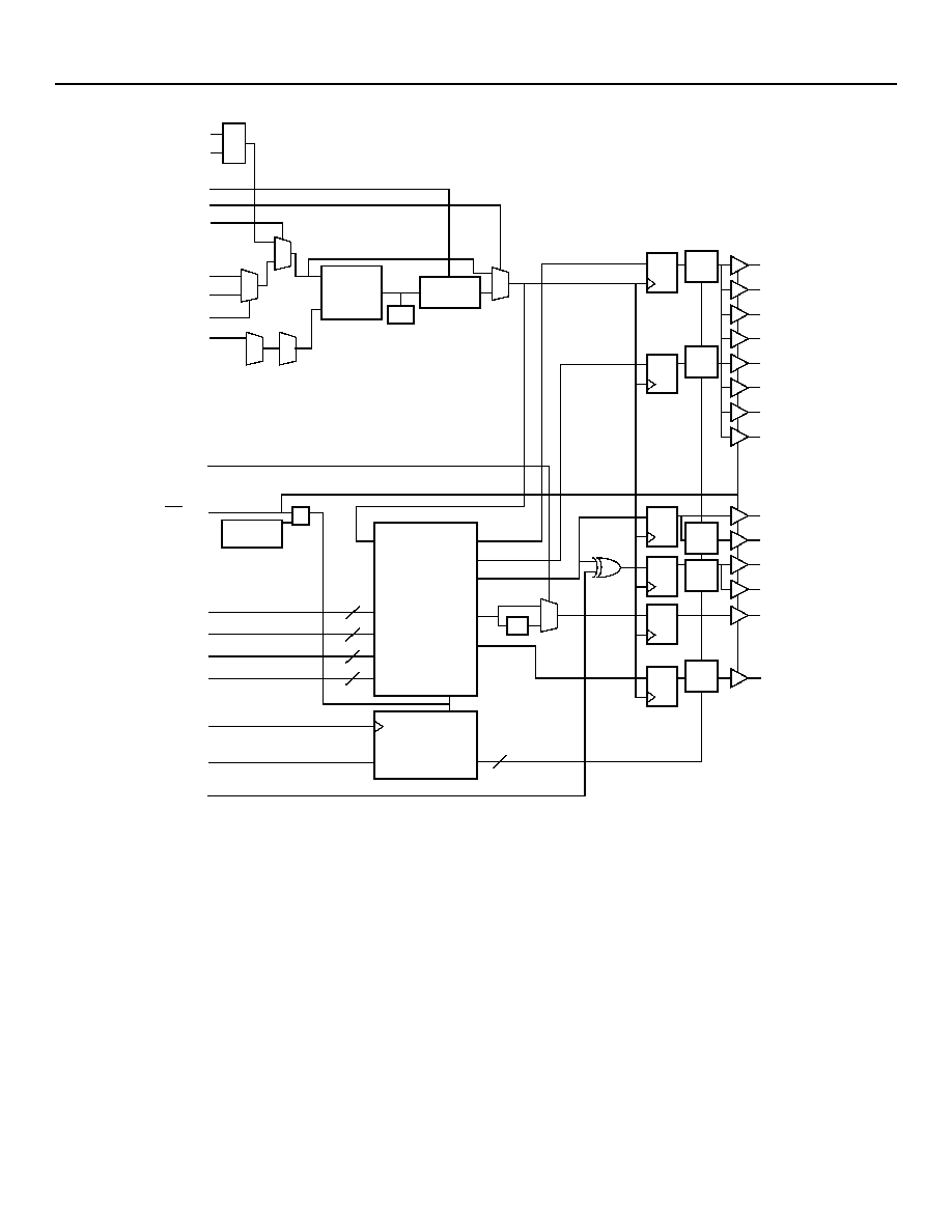
Figure 2-1. Logic Diagram ......................................................................................................................................................4
Figure 3-1. 52-Pin TQFPT ......................................................................................................................................................5
Figure 4-1. 100 MHz from 50 MHz Example ........................................................................................................................10
Figure 4-2. Pentium Compatible Clocks Example ................................................................................................................10
Figure 4-3. 20 MHz Source Example ...................................................................................................................................10
Figure 4-4. Skew Relative to Qa...........................................................................................................................................10
Figure 4-5. Phase Delay Example Using Two LCK4972s ....................................................................................................11
Figure 4-6. LCK4972 Timing ................................................................................................................................................12
Figure 4-7. Freeze Data Input Protocol ................................................................................................................................13
Figure 4-8. Power Supply Filter ............................................................................................................................................14
Figure 4-9. Dual Transmission Lines....................................................................................................................................15
Figure 4-10. Single vs. Dual Waveforms ..............................................................................................................................15
Figure 4-11. Optimized Dual Transmission Lines.................................................................................................................15
Tables
Page
Table 3-1. Pin Description.......................................................................................................................................................5
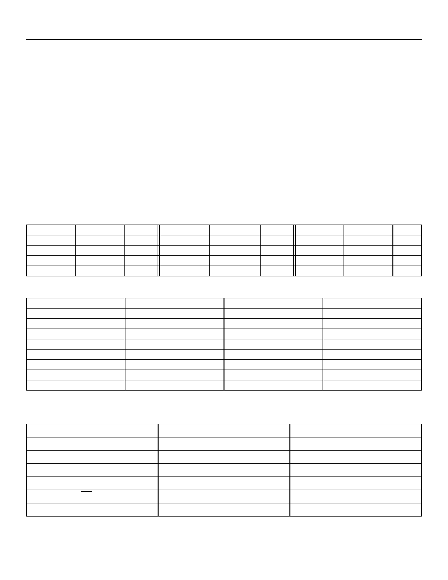
Table 4-1. Function Table for Qa, Qb, and Qc ........................................................................................................................7
Table 4-2. Function Table for QFB..........................................................................................................................................7
Table 4-3. Function Table for Logic Selection.........................................................................................................................7
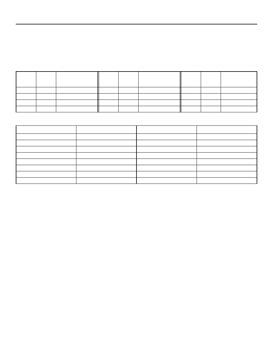
Table 4-4. Programmable Output Frequency Relationships for Qa, Qb, and Qc (VCO_Sel = 1) ...........................................8
Table 4-5. Programmable Output Frequency Relationships for QFB (VCO_Sel = 1).............................................................8
Table 4-6. Crystal Recommendations...................................................................................................................................12
Table 5-1. Absolute Maximum Ratings .................................................................................................................................15
Table 5-2. ESD Tolerance.....................................................................................................................................................15
Table 5-3. Thermal Parameter Values ..................................................................................................................................16
Table 6-1. PLL Input Reference Characteristics (TA = ≠40 ∞C to +85 ∞C) ............................................................................17
Table 6-2. dc Characteristics (TA = ≠40 ∞C to+85 ∞C, VDD = 3.3 V ± 5%) ...........................................................................17
Table 6-3. dc Characteristics (TA = ≠40 ∞C to +85 ∞C, VDD = 2.5 V ± 5%) ..........................................................................17
Table 6-4. ac Characteristics (TA = ≠40 ∞C to +85 ∞C, VDD = 3.3 V/2.5 V ± 5%).................................................................18
Table 8-1. LCK4972 Ordering Information............................................................................................................................20

Advance Data Sheet
March 26, 2004
LCK4972 Low-Voltage PLL Clock Driver
Agere Systems Inc.
3
2332 (F)
Figure 2-1. Logic Diagram
xtal1
xtal2
VCO_Sel
PLL_EN
REF_SEL
TCLK0
TCLK1
TCLK_Sel
Ext_FB
0
1
PHASE
DETECTOR
LPF
VCO
0
1
D Q
D Q
D Q
D Q
D Q
D Q
SYNC
Frz
SYNC
Frz
SYNC
Frz
SYNC
Frz
SYNC
Frz
Qa0
Qa1
Qa2
Qa3
Qb0
Qb1
Qb2
Qb3
Qc0
Qc1
Qc2
Qc3
QFB
QFB
QSync
0
1
˜
2
12
2
2
2
2
RESET
POWER-ON
˜
4,
˜
6,
˜
8,
˜
12
˜
4,
˜
6,
˜
8,
˜
10
˜
2,
˜
4,
˜
6,
˜
8
˜
4,
˜
6,
˜
8,
˜
10
SYNC PULSE
DATA
GENERATOR
OUTPUT DISABLE
CIRCUITRY
fselFB2
MR/OE
fsela0:1
fselb0:1
fselc0:1
fselFB0:1
Frz_Clk
Frz_Data
Inv_Clk

Advance Data Sheet
LCK4972 Low-Voltage PLL Clock Driver
March 26, 2004
4
4
Agere Systems Inc.
3 Pin Information
3.1 Pin Diagram
2331 (F)
Figure 3-1. 52-Pin TQFPT
40
38
35
34
33
32
31
30
29
28
27
37
V
SS
Ext_FB
V
DDI
V
DDO
fselFB0
36
Qb1
Qb0
V
DDO
QFB
V
SS
Qb3
Qb2
f
s
elb1
39
V
SS
14
17
18
19
20
21
22
23
24
25
15
V
SS
V
SS
I
n
v
_
Clk
Qc
1
16
Qc
3
fs
e
l
c
0
QS
y
n
c
Qc
0
V
DDO
Qc
2
V
DDO
fs
e
l
c
1
26
fs
e
l
FB
1
1
3
4
6
7
8
9
10
11
12
2
51
49
48
47
46
45
44
43
41
50
MROEB
V
SS
V
SS
Qa
2
Qa
0
Qa
3
f
s
elb0
Qa
1
f
s
ela0
42
5
fselFB2
Ref_Sel
TCLK0
xtal2
LCK4972
PLL_EN
TCLK1
Frz_Clk
Frz_Data
TCLK_Sel
xtal1
f
s
ela1
V
DD
O
V
SS
V
DD
O
13
V
DDA
52
VC
O_S
e
l

Advance Data Sheet
March 26, 2004
LCK4972 Low-Voltage PLL Clock Driver
Agere Systems Inc.
5
Table 3-1. Pin Description
Pin
Symbol
Type
I/O
*
Description
1, 15, 24, 30,
35, 39, 47, 51
V
SS
Ground
-- Ground.
2
MROEB
LVTTL
I
u
Master Reset and Output Enable Input.
0 = Outputs disabled (high-impedance state). During this condition the PLL
loop is open and the VCO will run at an indeterminate frequency.
1 = Normal operation (outputs active).
3
Frz_Clk
LVTTL
I
Freeze Mode.
4
Frz_Data
LVTTL
I
Freeze Mode.
5
fselFB2
LVTTL
I
u
Feedback Output Divider Function Select. This input, along with pins
fselFB0 and fselFB1, controls the divider function of the feedback bank of
outputs. See
Table 4-2
for more details.
6
PLL_EN
LVTTL
I
u
PLL Bypass Select.
0 = The internal PLL is bypassed and the selected reference input provides
the clocks to operate the device.
1 = The internal PLL provides the internal clocks to operate the device.
7
Ref_Sel
LVTTL
I
u
Reference Select Input. The Ref_Sel input controls the reference input to
the PLL.
0 = The input is selected by the TCLK_Sel input.
1 = The XTAL is selected.
8
TCLK_Sel
LVTTL
I
u
TCLK Select Input. The TCLK_Sel input controls which TCLK input will be
used as the reference input if Ref_Sel is set to 0.
0 = TCLK0 is selected.
1 = TCLK1 is selected.
9, 10
TCLK[0:1]
LVTTL
I
LVTLL Reference Input. These inputs provide the reference frequency for
the internal PLL when selected by Ref_Sel and TCLK_Sel.
11
xtal1
Analog
I
Xtal Reference Input. This input provides the reference frequency for the
internal PLL when selected by Ref_Sel.
12
xtal2
Analog
I
Xtal Reference Input. This input provides the reference frequency for the
internal PLL when selected by Ref_Sel.
13
V
DDA
Power
-- PLL Power.
14
Inv_Clk
LVTTL
I
u
Invert Mode. This input only affects the Qc bank.
0 = All outputs of the Qc bank are in the normal phase alignment.
1 = Qc2 and Qc3 are inverted from the normal phase of Qc0 and Qc1.
16, 18, 21, 23
Qc[3:0]
LVTTL
O Clock Output. These outputs, along with the Qa[0:3], Qb[0:3], and QFB
outputs, provide numerous divide functions determined by the fsela[0:3],
fselb[0:3], and the fselFB[0:2] See
Table 4-1
and
Table 4-2
for more details.
17, 22, 33,
37, 45, 49
V
DDO
Power
-- Output Buffer Power.
19, 20
fselc[1:0]
LVTTL
I
u
Output Divider Function Select. Each pair controls the divider function of
the respective bank of outputs. See
Table 4-1
for more details.
* U = Internal pull-up resistors (50 k
).

Advance Data Sheet
LCK4972 Low-Voltage PLL Clock Driver
March 26, 2004
6
6
Agere Systems Inc.
25
QSync
LVTTL
O Synchronous Pulse Output. This output is used for system
synchronization. See
Section 4.4 on page 10.
26
fselFB1
LVTTL
I
u
Feedback Output Divider Function Select. This input, along with pins
fselFB1 and fselFB2, controls the divider function of the feedback bank of
outputs. See
Table 4-2
for more details.
27
fselFB0
LVTTL
I
u
Feedback Output Divider Function Select. This input, along with pins
fselFB0 and fselFB2, controls the divider function of the feedback bank of
outputs. See
Table 4-2
for more details.
28
V
DDI
Power
-- PLL Power.
29
QFB
LVTTL
O Clock Output. This output, along with the Qa[0:3] and Qc[0:3] outputs,
provides numerous divide functions determined by the fsela[0:3], fselb[0:3],
and the fselFB[0:2]. See
Table 4-1
and
Table 4-2
for more details.
31
Ext_FB
LVTTL
I
PLL Feedback Input. This input is used to connect one of the clock
outputs (usually QFB) to the feedback input of the PLL.
32, 34, 36, 38
Qb[3:0]
LVTTL
O Clock Output. These outputs, along with the Qa[0:3], Qc[0:3], and QFB
outputs, provide numerous divide functions determined by the fsela[0:3],
fselb[0:3], and the fselFB[0:2]. See
Table 4-1
and
Table 4-2
for more
details.
40, 41
fselb[1:0]
LVTTL
I
Output Divider Function Select. Each pair controls the divider function of
the respective bank of outputs. See
Table 4-1
for more details.
42, 43
fsela[1:0]
LVTTL
I
Output Divider Function Select. Each pair controls the divider function of
the respective bank of outputs. See
Table 4-1
for more details.
44, 46, 48, 50
Qa[3:0]
LVTTL
O Clock Output. These outputs, along with the Qb[0:3], Qc[0:3], and QFB
outputs, provide numerous divide functions determined by the fsela[0:3],
fselb[0:3], and the fselFB[0:2]. See
Table 4-1
and
Table 4-2
for more
details.
52
VCO_Sel
LVTTL
I
u
VCO Frequency Select Input. This input selects the nominal operating
range of the VCO used in the PLL.
0 = The VCO range is 150 MHz--240 MHz.
1 = The VCO range is 200 MHz--480 MHz.
* U = Internal pull-up resistors (50 k
).
Table 3-1. Pin Description (continued)
Pin
Symbol
Type
I/O
*
Description

Advance Data Sheet
March 26, 2004
LCK4972 Low-Voltage PLL Clock Driver
Agere Systems Inc.
7
4 Functional Description
Using the select lines (fsela[1:0], fselb[1:0], fselc[1:0], and fselFB[2:0]), the following output frequency ratios between
outputs can be obtained:
1:1, 2:1, 3:1, 3:2, 4:1, 4:3, 5:1, 5:2, 5:3, 6:1, and 6:5
These ratios can be achieved by forcing the control signal low one clock edge before the coincident edges of outputs Qa
and Qc. The synchronization output indicates when these rising edges will occur. Selectability of feedback frequency is
independent of the output frequencies. Output frequencies can be odd or even multiples of the input reference clock, as
well as being less than the input frequency.
The power-on reset function is designed to reset the system after powerup for synchronization between QFB and other
outputs.
The LCK4972 has the ability to independently enable/disable each output through a serial input port. When disabled
(frozen), the outputs will freeze to the low state while internal state machines remain unaffected. When re-enabled, the
outputs initialize synchronously and in phase with those not reactivated. Freezing only happens when the outputs are in the
low state, preventing runt pulse generation, see Section
4.5 Output Freeze Circuitry on page 12
.
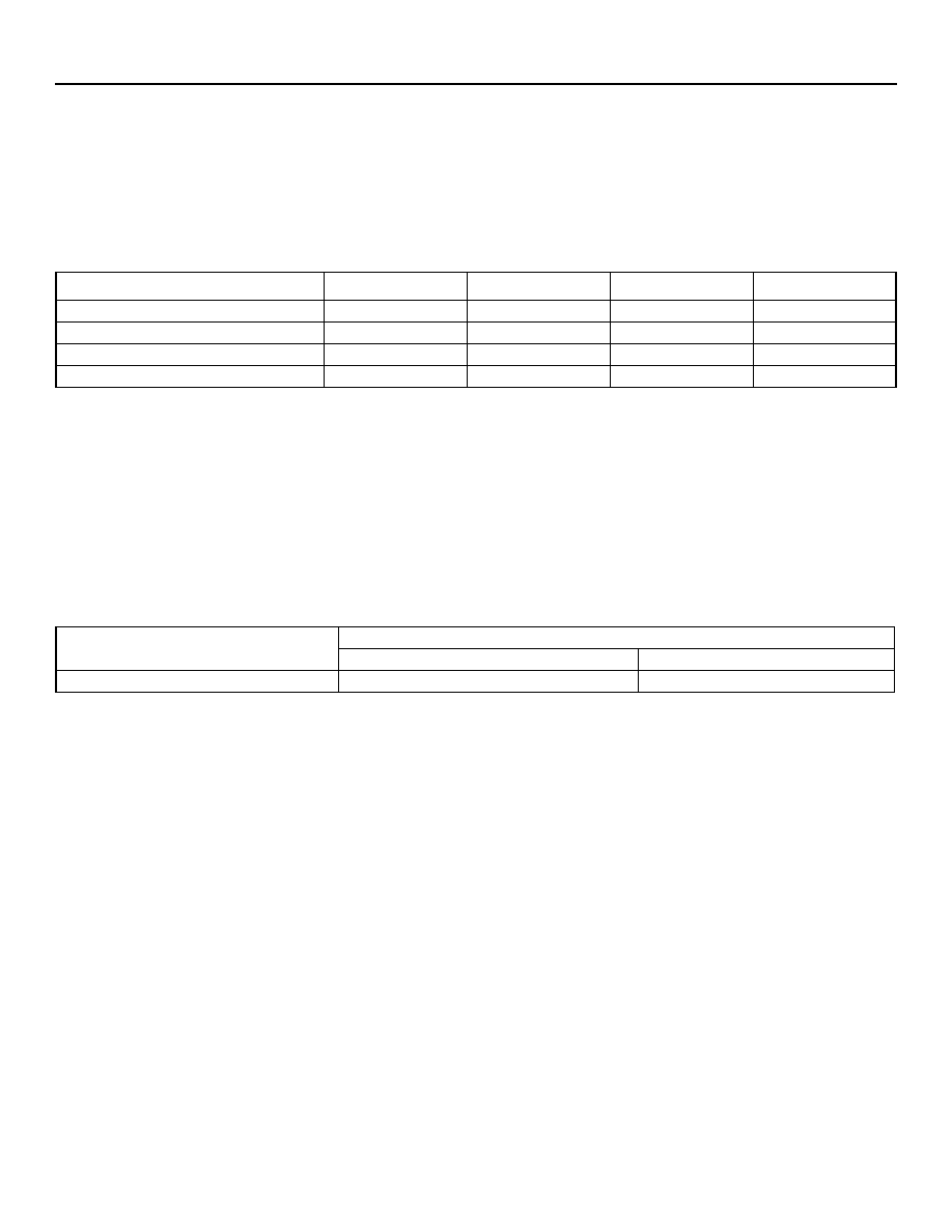
Table 4-1. Function Table for Qa, Qb, and Qc
Table 4-2. Function Table for QFB
1. If fselFB2 is set to 1, it may be necessary to apply a reset pulse after powerup in order to ensure synchronization between the QFB and other inputs.
Table 4-3. Function Table for Logic Selection
fsela1
fsela0
Qa
fselb1
fselb0
Qb
fselc1
fselc0
Qc
0
0
˜
4
0
0
˜
4
0
0
˜
2
0
1
˜
6
0
1
˜
6
0
1
˜
4
1
0
˜
8
1
0
˜
8
1
0
˜
6
1
1
˜
12
1
1
˜
10
1
1
˜
8
fselFB2
1
fselFB1
fselFB0
QFB
0
0
0
˜
4
0
0
1
˜
6
0
1
0
˜
8
0
1
1
˜
10
1
0
0
˜
8
1
0
1
˜
12
1
1
0
˜
16
1
1
1
˜
20
Control Pin
Logic 0
Logic 1
VCO_Sel
VCO/2
VCO
Ref_Sel
TCLK
Xtal
TCLK_Sel
TCLK0
TCLK1
PLL_EN
Bypass PLL
Enable PLL
MR/OE
Master reset/output high-Z
Enable outputs
Inv_Clk
Noninverted Qc2, Qc3
Inverted Qc2, Qc3

Advance Data Sheet
LCK4972 Low-Voltage PLL Clock Driver
March 26, 2004
8
8
Agere Systems Inc.
4.1 Device Programming
The LCK4972 contains three independent banks of four outputs as well as an independent PLL feedback output. The pos-
sible configurations make Agere Systems' LCK4972 one of the most versatile frequency programming devices. Table 4-4
shows various selection possibilities.
Table 4-4. Programmable Output Frequency Relationships for Qa, Qb, and Qc (VCO_Sel = 1)
Table 4-5. Programmable Output Frequency Relationships for QFB (VCO_Sel = 1)
To determine the relationship between the three banks, compare their divide ratios. For example, if a ratio of 5:3:2 is desired,
set Qa to
˜
10, Qb to
˜
6, and Qc to
˜
4. These selections would yield a 5:3:2 ratio.
For low frequency circumstances, the VCO_Sel pin allows the option of an additional
˜
2 to be added to the clock path. This
pin maintains the output relationships, but provides an extended clock range for the PLL. The feedback output is matched
to the input reference frequency after the output frequency relationship is set and VCO is in a stable range.
If, in the previous example, the input reference frequency were equal to the lowest output frequency, the output would be
set to
˜
10 mode. The fselFB2 input could be asserted to half the frequency if the needed feedback frequency is half of the
lowest frequency output. This multiplies the output frequencies by a factor of two, relative to the input reference frequency.
Assume the previously mentioned 5:3:2 ratio with the highest output frequency of 100 MHz. If the only available reference
frequency is 50 MHz, the setup of
Figure 4-1
can be used. The device provides 100 MHz, 66 MHz, and 40 MHz outputs, all
generated from the 50 MHz source.
Figure 4-2
and
Figure 4-3
also show possible configurations of the LCK4972.
fs
e
l
a
1
fs
e
l
a
0
Qa
f
selb
1
f
selb
0
Qb
fs
e
l
c
1
fs
e
l
c
0
Qc
0
0
VCO/4
0
0
VCO/4
0
0
VCO/2
0
1
VCO/6
0
1
VCO/6
0
1
VCO/4
1
0
VCO/8
1
0
VCO/8
1
0
VCO/6
1
1
VCO/12
1
1
VCO/10
1
1
VCO/8
fselFB2
fselFB1
fselFB0
QFB
0
0
0
VCO/4
0
0
1
VCO/6
0
1
0
VCO/8
0
1
1
VCO/10
1
0
0
VCO/8
1
0
1
VCO/12
1
1
0
VCO/16
1
1
1
VCO/20

Advance Data Sheet
March 26, 2004
LCK4972 Low-Voltage PLL Clock Driver
Agere Systems Inc.
9
4.2 Application Examples
Figure 4-3. 20 MHz Source Example
4.3 Typical Skew Example
Figure 4-4. Skew Relative to Qa
fsela0
fsela1
fselb0
fselb1
fselc0
fselc1
fselFB0
fselFB1
fselFB2
0
0
1
1
0
1
0
1
0
LCK4972
Qa
Qb
Qc
QFB
100 MHz
40 MHz
66.66 MHz
50 MHz
4
4
4
50 MHz
Input Ref
Ext_FB
VCO = 400 MHz
fsela0
fsela1
fselb0
fselb1
fselc0
fselc1
fselFB0
fselFB1
fselFB2
0
0
0
0
1
1
1
1
0
LCK4972
Qa
Qb
Qc
QFB
60 MHz (PROCESSOR)
60 MHz (PROCESSOR)
30 MHz (PCI)
24 MHz (FLOPPY DISK CLK)
4
4
4
24 MHz
Input Ref
Ext_FB
VCO = 240 MHz
Figure 4-1. 100 MHz from 50 MHz Example
Figure 4-2. Pentium Compatible Clocks Example
fsela0
fsela1
fselb0
fselb1
fselc0
fselc1
fselFB0
fselFB1
fselFB2
1
1
0
1
1
1
1
1
1
LCK4972
Qa
Qb
Qc
QFB
33 MHz (PCI)
50 MHz (PROCESSOR)
50 MHz (PROCESSOR)
20 MHz (ETHERNET)
4
4
4
20 MHz
Input Ref
Ext_FB
VCO = 400 MHz
≠100
≠75
≠50
≠25
0
25
50
75
100
Qc3
Qc2
Qc1
Qc0
Qb3
Qb2
Qb1
Qb0
Qa3
Qa2
Qa1
Qa0
ps
QFB

Advance Data Sheet
LCK4972 Low-Voltage PLL Clock Driver
March 26, 2004
10
10
Agere Systems Inc.
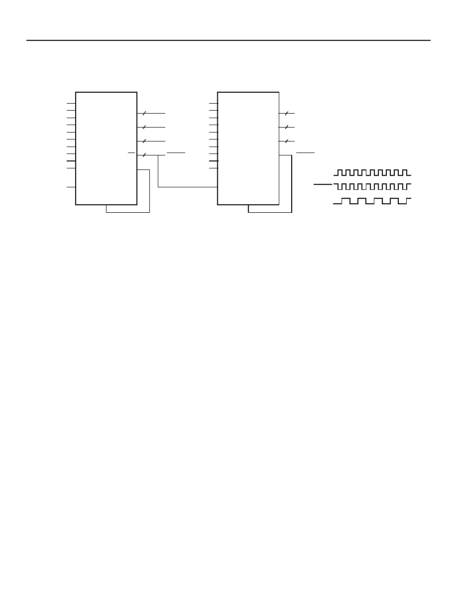
The Inv_Clk input pin, when asserted, will invert the Qc2 and Qc3 outputs. This inversion does not affect the output-output
skew of the device and allows for the development of 180∞ phase-shifted clocks. This output can also be used as a feedback
output or routed to a second PLL to generate early/late clocks. Figure 4-5 shows a 90∞ phase-shift configuration.
2337 (F)
Figure 4-5. Phase Delay Example Using Two LCK4972s
4.4 SYNC Output
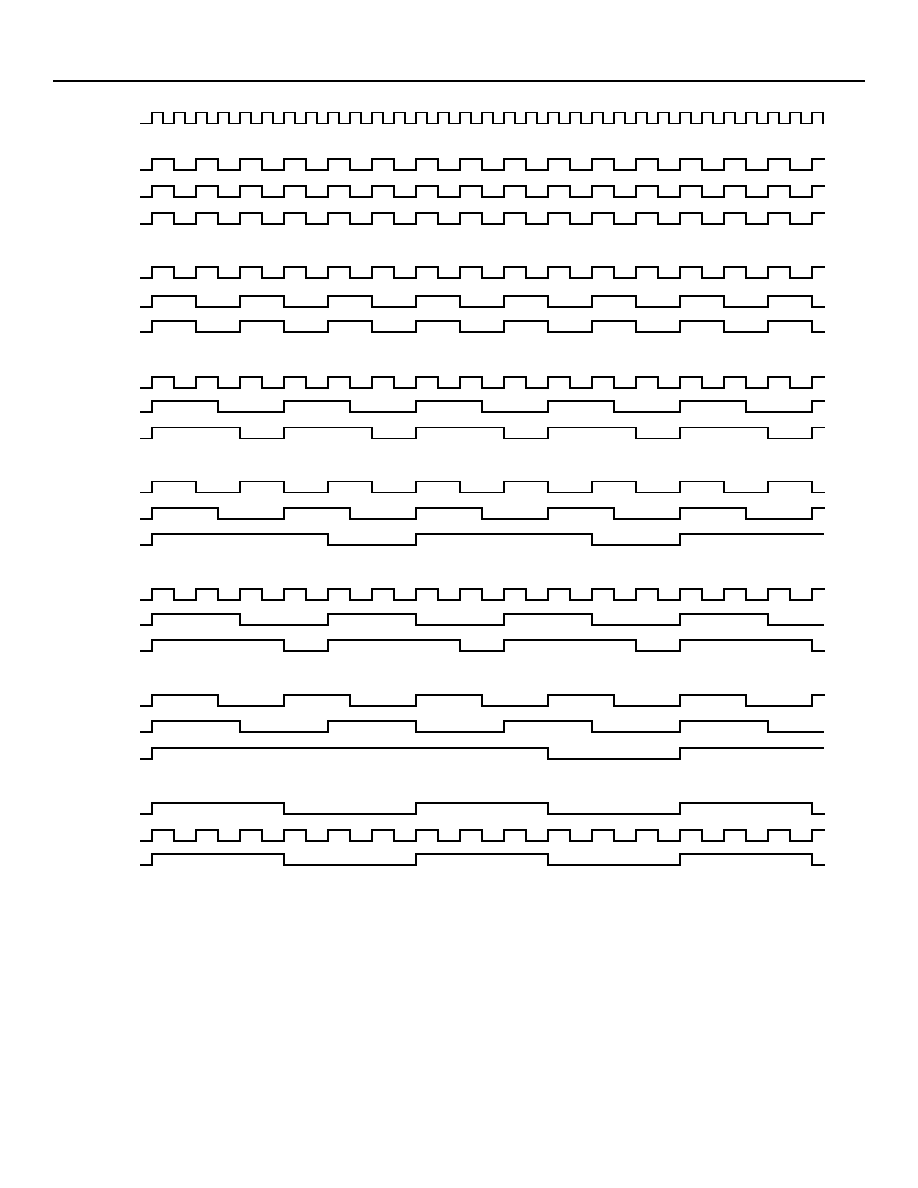
When the output frequencies are not integer multiples of each other, there is a need for a signal for synchronization purpos-
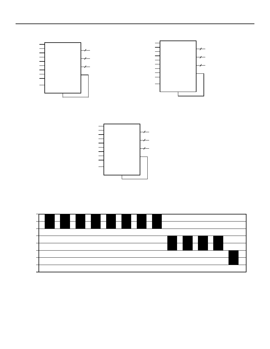
es. The SYNC output is designed to address this need. The Qa and Qc banks of outputs are monitored by the device, and
a low-going pulse (one period in duration, one period before the coincident rising edges of Qa and Qc) is provided. The du-
ration and placement of the pulse is dependent on the highest of Qa and Qc output frequencies. The timing diagram,
(
Figure 4-6
) shows the various waveforms for SYNC.
Note: SYNC is defined for all possible combinations of Qa and Qc, even though the lower frequency clock should be used
as a synchronizing signal in most cases.
fsela0
fsela1
fselb0
fselb1
fselc0
fselc1
fselFB0
fselFB1
fselFB2
0
0
0
0
1
0
0
0
0
LCK4972
Qa
Qb
Qc
Qc
66 MHz
66 MHz
66 MHz
66 MHz
4
4
2
66 MHz
Input Ref
Ext_FB
Inv_Clk
1
fsela0
fsela1
fselb0
fselb1
fselc0
fselc1
fselFB0
fselFB1
fselFB2
0
1
0
1
1
1
0
0
0
LCK4972
Qa
Qb
Qc
QFB
33 MHz SHIFTED 90∞
33 MHz SHIFTED 90∞
33 MHz SHIFTED 90∞
66 MHz
4
4
4
Input Ref
Ext_FB
Inv_Clk
0
QFB
66 MHz
66 MHz
33 MHz
SHIFTED 90∞
2

Advance Data Sheet
March 26, 2004
LCK4972 Low-Voltage PLL Clock Driver
Agere Systems Inc.
11
2333 (F)
Figure 4-6. LCK4972 Timing
fVCO
Qa
Qc
Sync
Qa
Qc
Sync
Qc(
˜
2)
Qa(
˜
6)
Sync
Qa(
˜
4)
Qc(
˜
6)
Sync
Qc(
˜
2)
Qa(
˜
8)
Sync
Qa(
˜
6)
Qc(
˜
8)
Sync
Qa(
˜
12)
Qc(
˜
2)
Sync
6:1 MODE
4:3 MODE
4:1 MODE
3:2 MODE
3:1 MODE
2:1 MODE
1:1 MODE

Advance Data Sheet
LCK4972 Low-Voltage PLL Clock Driver
March 26, 2004
12
12
Agere Systems Inc.
4.5 Output Freeze Circuitry
The new green classification for computers requires unique power management. The LCK4972's individual output enable
control allows software to implement unique power management. A serial interface was created to eliminate individual output
control at the cost of one pin per output.
The freeze control logic provides a mechanism for the LCK4972's clock outputs to be stopped in the logic 0 state.
The freeze mechanism allows serial loading of the 12-bit serial input register. This register contains one programmable
freeze enable bit for 12 of the 14 output clocks. The Qc0 and QFB outputs cannot be frozen with the serial port, which pre-
vents possible lock-up situations if there is an error in the serial input register. The user can also program a freeze by writing
0 to the respective freeze bit. Likewise, it can be programmed unfrozen by writing a 1 to that same bit.
Freeze logic cannot force a recently frozen clock to a logic 0 state before the time which it would normally transition to that
state. The logic will only maintain the frozen clock in logic 0. Similarly, the logic will not force a recently frozen clock to logic
1 before the time it would normally transition there. When the clock would normally be in a logic 0 state, the logic re-enables
the unfrozen clock, eliminating the possibility of runt clock pulses.
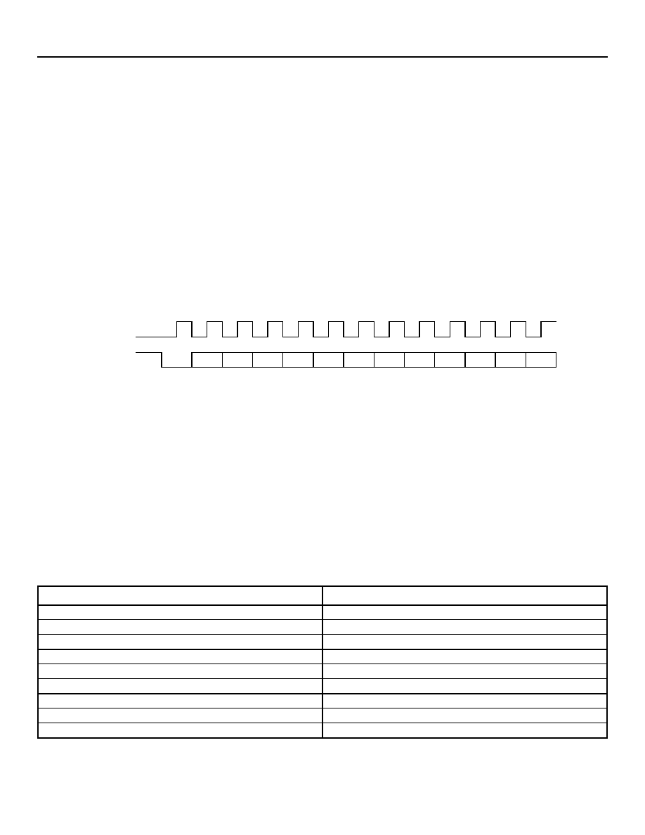
The user may write to the serial input register by supplying a logic 0 start bit followed (serially) by 12 NRZ freeze bits through
Frz_Data. The period of the Frz_Clk signal equals the period of each Frz_Data bit. The timing should be such that the
LCK4972 is able to sample each Frz_Data bit with the rising edge of the Frz_Clk (free running) signal.
Figure 4-7. Freeze Data Input Protocol
4.6 On-Board Crystal Oscillator
The LCK4972 features an on-board crystal oscillator for seed clock generation. The oscillator is self-contained. The only
external component required is the crystal. The circuit is a series resonant circuit, eliminating the need for large on-board
capacitors.
This series resonant design calls for a series resonant crystal, but most crystals are characterized in parallel resonant mode.
Physically, a parallel resonant crystal is no different from a series resonant crystal. Overall, a parallel crystal can be used
with this device with a small frequency error due to the actual series resonant frequency of the parallel resonant crystal. A
parallel specified crystal will exhibit an oscillatory frequency ±100 ppm lower than the specified value. This translates to in-
effectual kHz inaccuracies, which will not effect the device.
Table 4-6. Crystal Recommendations
Parameter
Value
Crystal Cut
Functional AT cut
Resonance
Series resonance
Frequency Tolerance
±75 ppm at 25 ∞C
Frequency/Temperature Stability
±150 ppm at 0 ∞C--70 ∞C
Operating Range
0 ∞C--70 ∞C
Shunt Capacitance
5 pF--7 pF
Equivalent Series Resistance (ESR)
50
--80
max
Correlation Drive Level
100
µ
W
Aging
5 ppm/year (first 3 years)
QA0 QA1 QA2 QA3 QB0 QB1 QB2 QB3 QC1 QC2 QC3
QSYNC
START
Frz_Data
Frz_Clk
Frz_Data

Advance Data Sheet
March 26, 2004
LCK4972 Low-Voltage PLL Clock Driver
Agere Systems Inc.
13
4.7 Power Supply Filtering
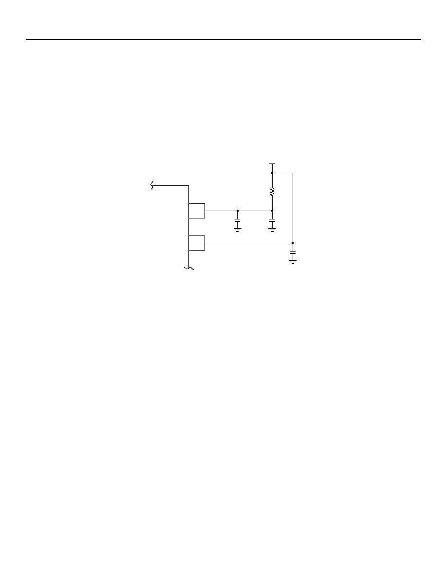
The LCK4972 is a mixed-signal product which is susceptible to random noise, especially when this noise is on the power
supply pins. To isolate the output buffer switching from the internal phase-locked loop, the LCK4972 provides separate pow-
er supplies for the internal PLL (V
DDA
) and for the output buffers (V
DDO
). In a digital system environment, besides this iso-
lation technique, it is highly recommended that both V
DDA
and V
DD
power supplies be filtered to reduce the random noise
as much as possible.
Figure 4-8
illustrates a typical power supply filter scheme. Due to its susceptibility to noise with spectral content in this range,
a filter for the LCK4972 should be designed to target noise in the 100 kHz to 10 MHz range. The RC filter in
Figure 4-8
will
provide a broadband filter with approximately 100:1 attenuation for noise with spectral content above 20 kHz. More elaborate
power supply schemes may be used to achieve increased power supply noise filtering.
2344 (F)
Figure 4-8. Power Supply Filter
0.01
µ
F
22
µ
F
R
S
= 5
--10
V
DD
V
DDA
LCK4972
0.01
µ
F
3.3 V

Advance Data Sheet
LCK4972 Low-Voltage PLL Clock Driver
March 26, 2004
14
14
Agere Systems Inc.
4.8 Driving Transmission Lines
The output drivers of the LCK4972 were designed for the lowest impedance possible for maximum flexibility. With the
LCK4972's 7
impedance, the drivers can accommodate either parallel or series terminated transmission lines.
Point-to-point distribution of signals is the preferred method in today's high-performance clock networks. Series-terminated
or parallel-terminated lines can be used in a point-to-point scheme. The parallel configuration terminates the signal at the
end of the line with a 50
resistance to V
DD
/2. Only one terminated line can be driven by each output of the LCK4972 due
to the high level of dc current drawn.
In a series-terminated case, there is no dc current draw; the outputs can drive multiple series-terminated lines, see below.
2340 (F)
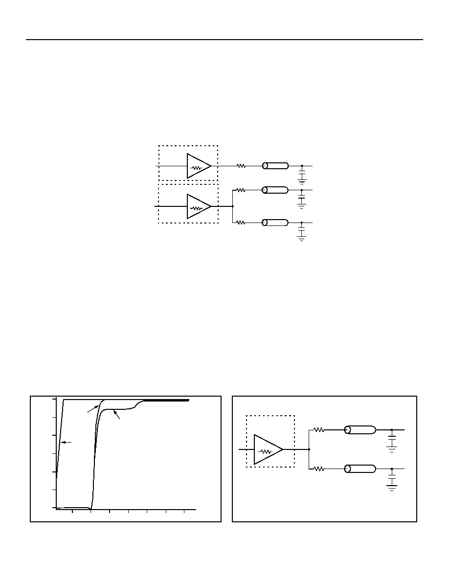
Figure 4-9. Dual Transmission Lines
The waveform plots of
Figure 4-10
show the simulated results of a single output versus a two-line output. A 43 ps delta exists
between the two differently loaded outputs that can be seen in the figure. This implies that dual-line driving need not be used
in order to maintain tight output-to-output skew. The step in the figure shows an impedance mismatch caused when looking
into the driver. The parallel combination in Figure 4-9 plus the output resistance do not equal the parallel combination of the
line impedances. The voltage wave down the lines will equal the following:
VL = VS (Z
0
/R
S
+ R
0
+ Z
0
) = 3.0 (25/53.5) = 1.4 V
The voltage will double at the load-end to 2.8 V, due to the near-unity reflection coefficient. It then continues to increment
towards 3.0 V in one-round trip delay steps (4 ps). This step will not cause any false clock triggering, but some users may
not want these reflections on the line.
Figure 4-11
shows a possible configuration to eliminate these reflections. In this sce-
nario, the series terminating resistors are reduced so the line impedance is matched when the parallel combination is added
to the output buffer.
Z
O
= 50
R
S
= 43
7
LCK4972
OUTPUT
BUFFER
IN
Z
O
= 50
R
S
= 43
7
LCK4972
OUTPUT
BUFFER
IN
Z
O
= 50
R
S
= 43
OUTA
OUTB0
OUTB1
V
O
LTAGE (V)
OUTB
t
D
= 3.9386
OUTA
t
D
= 3.8956
IN
3.0
2.5
2.0
1.5
1.0
0
2
4
6
8
10
12
14
0.5
TIME (ns)
Z
O
= 50
R
S
= 36
7
LCK4972
OUTPUT
BUFFER
Z
O
= 50
R
S
= 36
7
+
36
36
= 50
50
25
= 25
Figure 4-10. Single vs. Dual Waveforms
Figure 4-11. Optimized Dual Transmission Lines

Advance Data Sheet
March 26, 2004
LCK4972 Low-Voltage PLL Clock Driver
Agere Systems Inc.
15
5 Absolute Maximum Ratings
Stresses which exceed the absolute maximum ratings can cause permanent damage to the device. These are absolute
stress ratings only. Functional operation of the device is not implied at these or any other conditions in excess of those given
in the operational sections of the data sheet. Exposure to absolute maximum ratings for extended periods of time can ad-
versely affect device reliability.
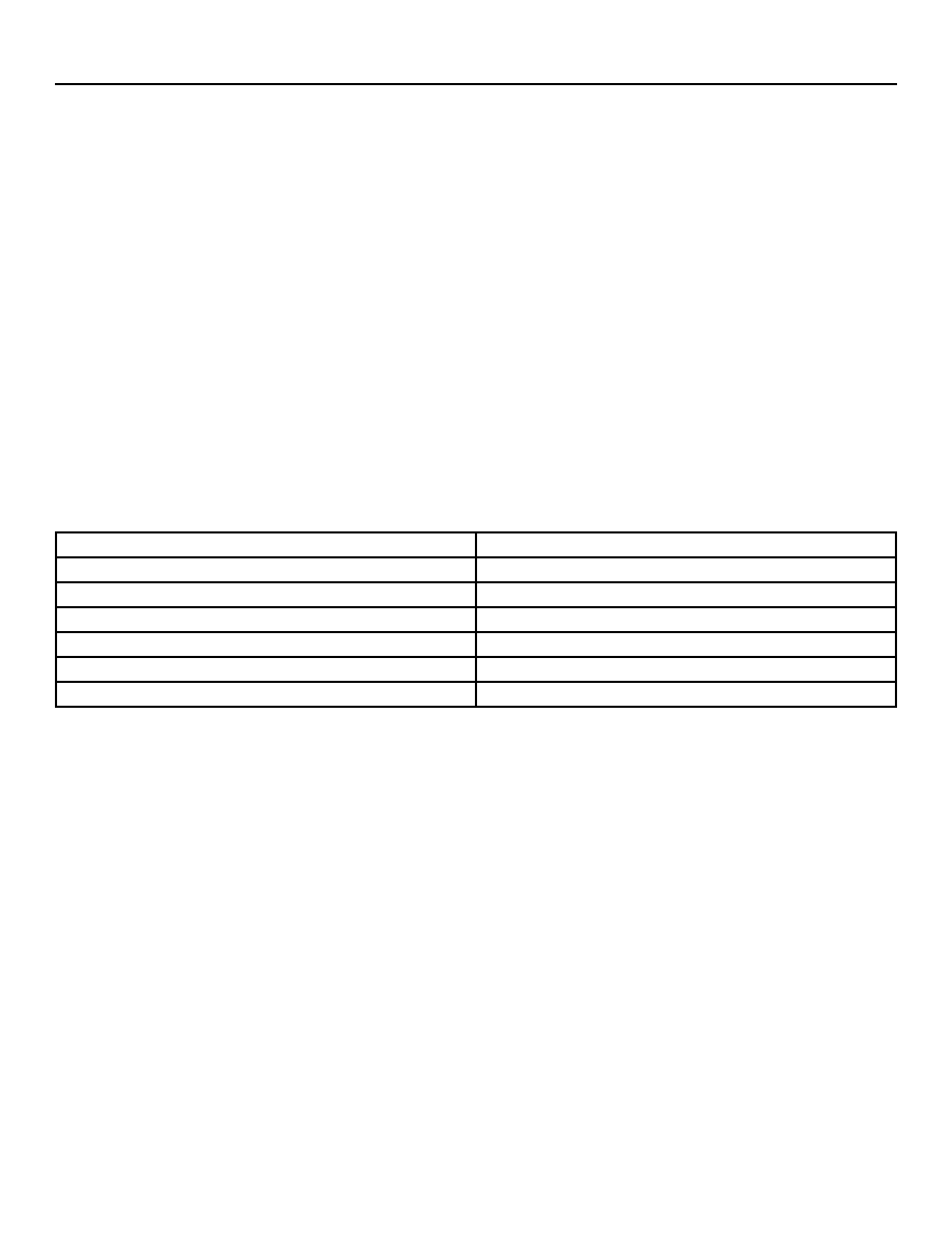
Table 5-1. Absolute Maximum Ratings
5.1 Handling Precautions
Although electrostatic discharge (ESD) protection circuitry has been designed into this device, proper precautions must be
taken to avoid exposure to ESD and electrical overstress (EOS) during all handling, assembly, and test operations. Agere
employs both a human-body model (HBM) and a charged-device model (CDM) qualification requirement in order to
determine ESD-susceptibility limits and protection design evaluation. ESD voltage thresholds are dependent on the circuit
parameters used in each of the models, as defined by JEDEC's JESD22-A114 (HBM) and JESD22-C101 (CDM)
standards.
5.2 Thermal Parameters (Definitions and Values)
System and circuit board level performance depends not only on device electrical characteristics, but also on device thermal
characteristics. The thermal characteristics frequently determine the limits of circuit board or system performance, and they
can be a major cost adder or cost avoidance factor. When the die temperature is kept below 125 ∞C, temperature activated
failure mechanisms are minimized. The thermal parameters that Agere provides for its packages help the chip and system
designer choose the best package for their applications, including allowing the system designer to thermally design and in-
tegrate their systems.
It should be noted that all the parameters listed below are affected, to varying degrees, by package design (including paddle
size) and choice of materials, the amount of copper in the test board or system board, and system airflow.
JA
- Junction to Air Thermal Resistance
JA
is a number used to express the thermal performance of a part under JEDEC standard natural convection conditions.
JA
is calculated using the following formula:
JA
= (T
J
≠ T
amb
) / P; where P = power
JMA
- Junction to Moving Air Thermal Resistance
JMA
is effectively identical to
JA
but represents performance of a part mounted on a JEDEC four layer board inside a wind
tunnel with forced air convection.
JMA
is reported at airflows of 200 LFPM and 500 LFPM (linear feet per minute), which
roughly correspond to 1 m/s and 2.5 m/s (respectively).
JMA
is calculated using the following formula:
JMA
= (T
J
≠ T
amb
) / P
Parameter
Symbol
Min
Max
Unit
Supply Voltage
V
DD
≠0.3
4.6
V
Input Voltage
V
I
≠0.3
V
DD
+ 0.3
V
Input Current
I
IN
--
±
20
mA
Storage Temperature Range
T
stg
≠40
125
∞C
Table 5-2. ESD Tolerance
Device
Minimum Threshold
HBM
CDM
LCK4972
>2500 V
>1000 V

Advance Data Sheet
LCK4972 Low-Voltage PLL Clock Driver
March 26, 2004
16
16
Agere Systems Inc.
JC
- Junction to Case Thermal Resistance
JC
is the thermal resistance from junction to the top of the case. This number is determined by forcing nearly 100% of the
heat generated in the die out the top of the package by lowering the top case temperature. This is done by placing the top
of the package in contact with a copper slug kept at room temperature using a liquid refrigeration unit.
JC
is calculated using
the following formula:
JC
= (T
J
≠ T
C
) / P
JB
- Junction to Board Thermal Resistance
JB
is the thermal resistance from junction to board. This number is determined by forcing the heat generated in the die out
of the package through the leads or balls by lowering the board temperature and insulating the package top. This is done
using a special fixture, that keeps the board in contact with a water chilled copper slug around the perimeter of the package
while insulating the package top.
JB
is calculated using the following formula:
JB
= (T
J
≠ T
B
) / P
JT
JT
correlates the junction temperature to the case temperature. It is generally used by the customer to infer the junction
temperature while the part is operating in their system. It is not considered a true thermal resistance.
JT
is calculated using
the following formula:
JT
= (T
J
≠ T
C
) / P
Table 5-3. Thermal Parameter Values
Parameter
Temperature ∞C/Watt
JA
51.11
JMA
(1 m/s)
TBD
JMA
(2.5 m/s)
TBD
JC
14.81
JB
40.23
JT
1

Advance Data Sheet
March 26, 2004
LCK4972 Low-Voltage PLL Clock Driver
Agere Systems Inc.
17
6 Electrical Characteristics
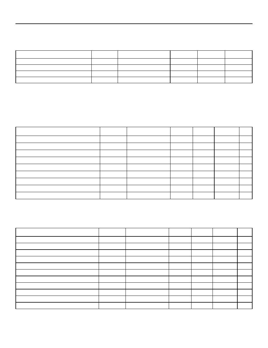
Table 6-1. PLL Input Reference Characteristics (T
A
= ≠40 ∞C to +85 ∞C)
1. Maximum input reference frequency is limited by VCO lock range and the feedback driver or 100 MHz. Minimum input reference frequency is limited by
the VCO lock range and the feedback divider.
2. See Section
On-Board Crystal Oscillator, on page 12
for more crystal information.
6.1 dc Characteristics
Table 6-2. dc Characteristics (T
A
= ≠40 ∞C to+85 ∞C, V
DD
= 3.3 V
±
5%)
1. The LCK4972 inputs can drive a series of parallel terminated transmission lines on the incident edge.
2. Inputs have pull-up/pull-down resistors, which affect input current.
3. Qa = Qb = Qc = 50 MHz, unloaded outputs.
Table 6-3. dc Characteristics (T
A
= ≠40 ∞C to +85 ∞C, V
DD
= 2.5 V
±
5%)
* The LCK4972 is capable of driving 50
transmission lines on the incident edge. Each output drives one 50
parallel terminated transmission line to a
termination voltage of V
TT
. Alternatively, the device drives up to two 50
series terminated transmission lines per output.
Qa = Qb = Qc = 50 MHz, unloaded outputs.
Parameter
Symbol
Condition
Min
Max
Unit
TCLK Input Rise/Fall
tr, tf
--
--
3.0
ns
Reference Input Frequency
f
ref
--
--
1
--
1
MHz
Reference Input Duty Cycle
t
refDC
--
25
75
%
Crystal Oscillator Frequency
t
xtal
--
2
10
25
MHz
Parameter
Symbol
Condition
Min
Typ
Max
Unit
Input High Voltage
V
IH
--
2.0
--
3.6
V
Input Low Voltage
V
IL
--
--
--
0.8
V
Output High Voltage
V
OH
I
OH
= ≠24 mA
1
2.4
--
--
V
Output Low Voltage
V
OL
I
OL
= 24 mA
1
--
--
0.5
V
Input Current
I
IN
--
2
--
--
±
120
µA
Maximum Supply Current
I
DD
All V
DD
pins
--
130
160
mA
Analog V
DD
Current
I
DDA
V
DDA
pin only
3
--
60
85
mA
Input Capacitance
C
IN
--
--
--
4
pF
Power Dissipation Capacitance
C
pd
Per output
--
25
--
pF
Parameter
Symbol
Condition
Min
Typ
Max
Unit
PLL Supply Voltage
V
DD_PLL
LVCMOS
2.325
--
V
DD
V
Input High Voltage
V
IH
LVCMOS
1.7
--
V
DD
+ 0.3
V
Input Low Voltage
V
IL
LVCMOS
≠0.3
--
0.7
V
Output High Voltage
V
OH
I
OH
= ≠15 mAS*
1.8
--
--
V
Output Low Voltage
V
OL
I
OL
= 15 mA
--
--
0.6
V
Output Impedance
Z
OUT
--
17
--
20
W
Input Current
I
IN
V
IN
= V
DD
or GND
--
--
±
120
µA
Analog V
DD
Current
I
DDA
V
DDA
pin only
--
60
85
mA
Maximum Supply Current
I
DD
All V
DD
Pins
--
130
160
mA
Input Capacitance
C
IN
--
--
--
4
pF
Power Dissipation Capacitance
C
pd
Per output
--
25
--
pF

Advance Data Sheet
LCK4972 Low-Voltage PLL Clock Driver
March 26, 2004
18
18
Agere Systems Inc.
6.2 ac Characteristics
Table 6-4. ac Characteristics (T
A
= ≠40 ∞C to +85 ∞C, V
DD
= 3.3 V/2.5 V
±
5%)
1
1. ac characteristics apply for parallel output termination of 50
to V
TT
.
2. In bypass mode, the LCK4972 divides the input reference clock.
3. The input reference frequency must match the VCO lock range divided by the total feedback divider ratio: f
REF
= f
VCO
˜
(M x VCO
_SEL
).
4. The crystal frequency range must meet the interface frequency range and the VCO lock range divided by the feedback divider ratio:
f
XTAL
(min, max) = f
VCO
(min, max)
˜
(M x VCO
_SEL
) and 10 MHz
f
XTAL
25 MHz.
5.
t
JIT (CC) is valid for a VCO frequency of 400 MHz with QFB = to divide by 4.
Parameter
Symbol
Condition
Min
Typ
Max
Unit
Input Reference Frequency:
˜
4 feedback
˜
6 feedback
˜
8 feedback
˜
10 feedback
˜
12 feedback
˜
16 feedback
˜
20 feedback
f
REF
PLL locked
37.5
25.0
18.75
15.0
12.5
9.4
7.5
--
--
--
--
--
--
--
120.0
80.0
60.0
48.0
40.0
30.0
24.0
MHz
Input Reference Frequency in PLL Bypass Mode
2
f
REF
PLL bypass
--
--
250
MHz
VCO Frequency Range
3
f
VCO
--
150
--
480
MHz
Crystal Internal Frequency Range
4
f
XTAL
--
10
--
25
MHz
Output Frequency:
˜
2 output
˜
4 output
˜
6 output
˜
8 output
˜
10 output
˜
12 output
f
MAX
PLL locked
75.0
37.5
25.0
18.75
15.0
12.5
--
--
--
--
--
--
240.0
120.0
80.0
60.0
48.0
40.0
MHz
Serial Interface Clock Frequency
f
STOP_CLK
--
--
--
20
MHz
Reference Input Duty Cycle
f
REFDC
--
25
--
75
%
CCLKx Input Rise/Fall Time
t
R
, t
F
20% to 80%
--
--
1.0
ns
Propagation Delay (static phase offset) CCLKx or FB_IN
t(
)
PLL locked
--
--
150
ps
Output-to-Output Skew
t
SK(O)
--
--
--
250
ps
Output Duty Cycle
DC
--
47
50
53
%
Output Rise/Fall Time
t
R
, t
F
20% to 80%
0.1
--
1.0
ns
Output Disable Time
t
PLZ, HZ
--
--
--
8
ns
Output Enable Time
t
PZL, LZ
--
--
--
8
ns
Cycle-to-Cycle Jitter
5
t
JIT(CC)
--
--
150
200
ps
Period Jitter
t
JIT(PER)
--
--
--
150
ps
I/O Phase Jitter
t
JIT(
)
--
--
--
150
ps
Maximum PLL Lock Time
t
LOCK
--
--
10
--
ms

Advance Data Sheet
March 26, 2004
LCK4972 Low-Voltage PLL Clock Driver
Agere Systems Inc.
19
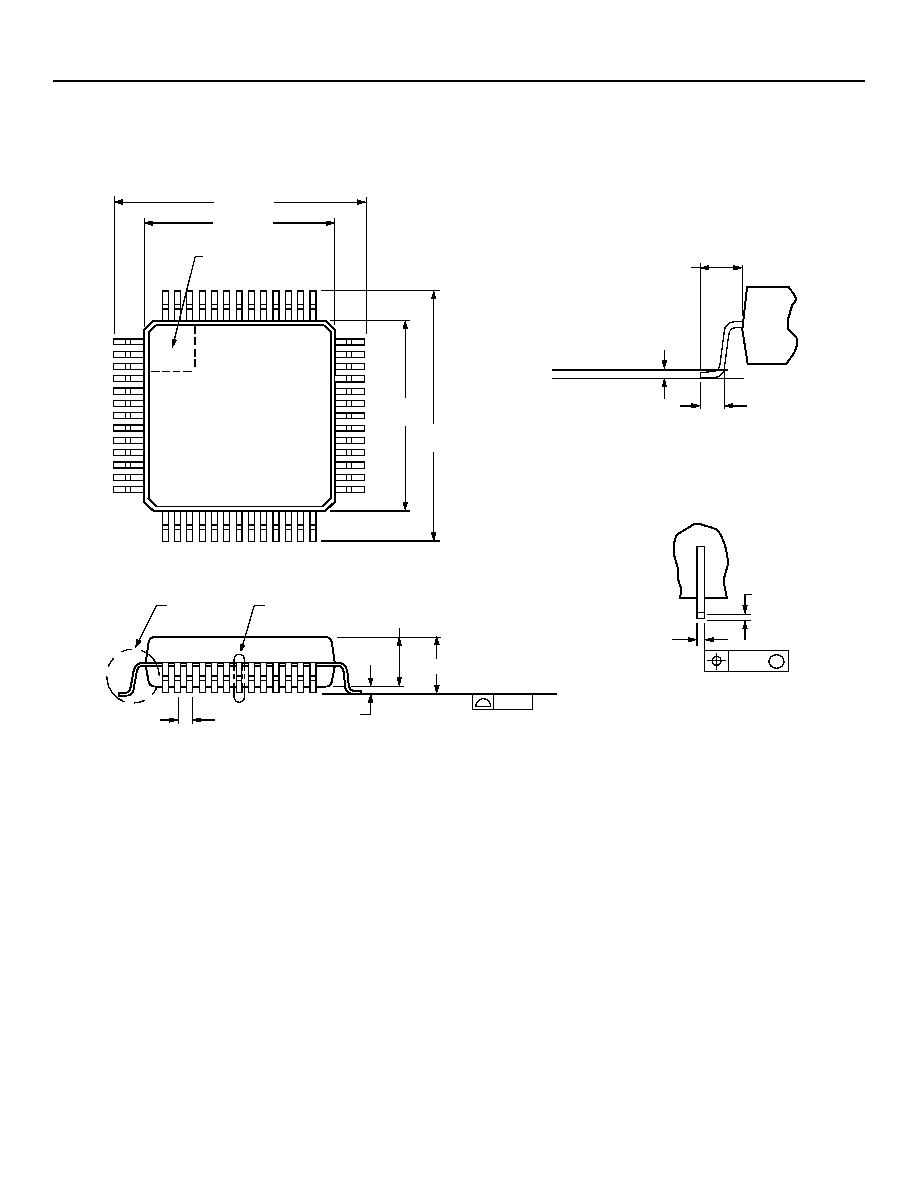
7 Outline Diagram
52-pin TQFPT package outline. All dimensions are in millimeters.
PIN #1
IDENTIFIER ZONE
26
10.00
1
52
40
13
14
39
27
12.00
1.20 MAX
SEATING PLANE
DETAIL A
0.08
1.00 ± 0.05
0.65 TYP
0.05/0.15
DETAIL B
DETAIL B
0.22/0.38
0.08
M
0.09/0.20
DETAIL A
0.45/0.75
GAGE PLANE
SEATING PLANE
1.00 REF
0.25
12.00
10.00

Agere Systems Inc. reserves the right to make changes to the product(s) or information contained herein without notice. No liability is assumed as a result of their use or application.
Agere is a registered trademark of Agere Systems Inc. Agere Systems and the Agere logo are trademarks of Agere Systems Inc.
Copyright © 2004 Agere Systems Inc.
All Rights Reserved
March 26, 2004
DS04-066LCK (Replaces DS03-014LCK)
For additional information, contact your Agere Systems Account Manager or the following:
INTERNET:
http://www.agere.com
E-MAIL:
docmaster@agere.com
N. AMERICA:
Agere Systems Inc., Lehigh Valley Central Campus, Room 10A-301C, 1110 American Parkway NE, Allentown, PA 18109-9138
1-800-372-2447, FAX 610-712-4106 (In CANADA: 1-800-553-2448, FAX 610-712-4106)
ASIA:
Agere Systems Hong Kong Ltd., Suites 3201 & 3210-12, 32/F, Tower 2, The Gateway, Harbour City, Kowloon
Tel. (852) 3129-2000, FAX (852) 3129-2020
CHINA: (86) 21-54614688 (Shanghai), (86) 755 25881122 (Shenzhen)
JAPAN: (81) 3-5421-1600 (Tokyo), KOREA: (82) 2-767-1850 (Seoul), SINGAPORE: (65) 778-8833, TAIWAN: (886) 2-2725-5858 (Taipei)
EUROPE:
Tel. (44) 1344 296 400
8 Ordering Information
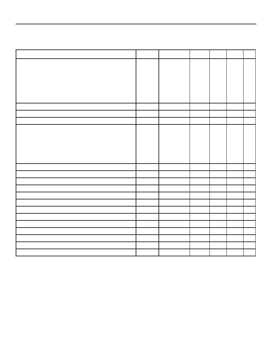
Table 8-1. LCK4972 Ordering Information
Device
Package Type
Comcode
Delivery
LCK4972
TQFPT
700010364
Tray


