 | –≠–ª–µ–∫—Ç—Ä–æ–Ω–Ω—ã–π –∫–æ–º–ø–æ–Ω–µ–Ω—Ç: LCK4973 | –°–∫–∞—á–∞—Ç—å:  PDF PDF  ZIP ZIP |

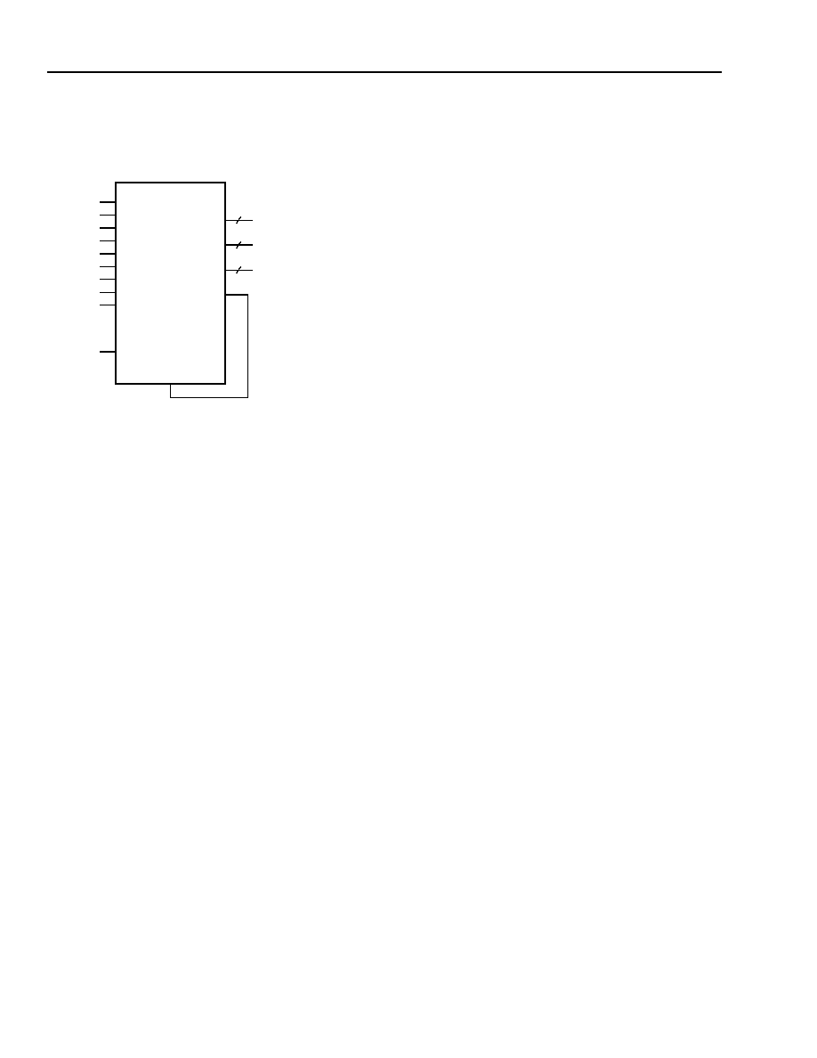
Data Sheet
February 2003
LCK4973
Low-Voltage PLL Clock Driver
Features
s
Fully integrated PLL.
s
Output frequency up to 240 MHz.
s
Compatible with PowerPC
Æ
and Pentium
Æ
microprocessors.
s
52-pin TQFPT.
s
3.3 V/2.5 V power supply.
s
Pin compatible with 973 type devices.
s
±100 ps typical cycle-to-cycle jitter.
s
Output skews of less than 250 ps.
Description
Agere Systems' LCK4973 is a 3.3 V/2.5 V,
PLL-based clock driver for high-performance RISC or
CISC processor-based systems. The LCK4973 has
output frequencies of up to 240 MHz and skews of
less than 250 ps, making it ideal for synchronous
systems. The LCK4973 contains 12 low-skew
outputs and a feedback/sync output for flexibility and
simple implementation.
There is a robust level of frequency programmability
between the 12 low-skew outputs in addition to the
input/output relationships. This allows for very
flexible programming of the input reference versus
the output frequency. The LCK4973 contains a
flexible output enable and disable scheme. This
helps execute system debug as well as offer multiple
powerdown schemes, which meet green-class
machine requirements.
The LCK4973 features a power-on reset function,
which automatically resets the device on powerup,
providing automatic synchronization between QFB
and other outputs.
The LCK4973 is 3.3 V/2.5 V compatible and requires
no external loop filters. It has the capability of driving
50
transmission lines. Series terminated lines have
the ability of driving two 50
lines in parallel,
effectively doubling the fanout.

2
Agere Systems Inc.
Data Sheet
February 2003
Low-Voltage PLL Clock Driver
LCK4973
Pin Information
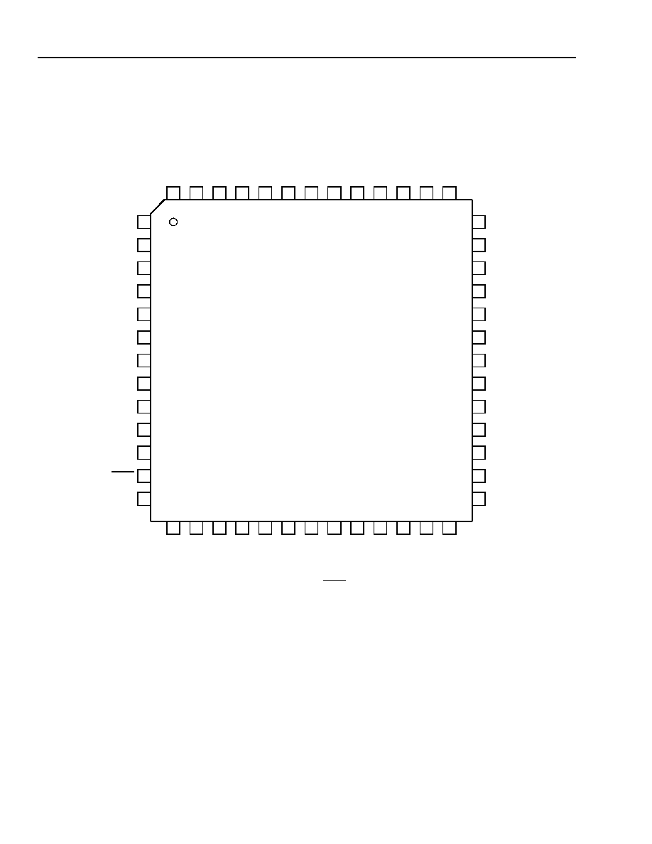
Pin Diagram
2331.a (F)
Note: All inputs have internal pull-up resistors (50 k
) except for PCLK and PCLK.
Figure 1. 52-Pin TQFPT
40
38
35
34
33
32
31
30
29
28
27
37
V
SS
Ext_FB
V
DDI
V
DDO
fselFB0
36
Qb1
Qb0
V
DDO
QFB
V
SS
Qb3
Qb2
fs
e
l
b
1
39
V
SS
14
17
18
19
20
21
22
23
24
25
15
V
SS
V
SS
Inv
_
Clk
Qc
1
16
Qc
3
fs
e
l
c
0
Q
S
ync
Qc
0
V
DD
O
Qc
2
V
DDO
fs
e
l
c
1
26
fs
e
l
F
B
1
1
3
4
6
7
8
9
10
11
12
2
51
49
48
47
46
45
44
43
41
50
MROEB
V
SS
V
SS
Qa
2
Qa
0
Qa
3
fs
e
l
b
0
Qa
1
fs
e
l
a
0
42
5
fselFB2
Ref_Sel
TCLK0
PCLK
LCK4973
PLL_EN
TCLK1
Frz_Clk
Frz_Data
TCLK_Sel
PCLK
fs
e
l
a
1
V
DDO
V
SS
V
DDO
13
V
DDA
52
VC
O_
S
e
l

Agere Systems Inc.
3
Data Sheet
February 2003
Low-Voltage PLL Clock Driver
LCK4973
Pin Information
(continued)
Pin Descriptions
Table 1. Pin Descriptions
Pin
Symbol
Type
I/O
Description
1, 15,
24, 30,
35, 39,
47, 51
V
SS
Ground
-- Ground.
2
MROEB
LVTTL
I
Master Reset and Output Enable Input.
Note: When MR/OE is set high, the PLL will have been disturbed and
the outputs will be at an indeterminate frequency until MR/OE is
relocked.
3
Frz_Clk
LVTTL
I
Freeze Mode.
4
Frz_Data
LVTTL
I
Freeze Mode.
5
fselFB2
LVTTL
I
Feedback Output Divider Function Select. This input, along with pins
fselFB0 and fselFB1, controls the divider function of the feedback bank
of outputs. See Table 3 for more details.
6
PLL_EN
LVTTL
I
PLL Bypass Select.
0 = The internal PLL is bypassed and the selected reference input
provides the clocks to operate the device.
1 = The internal PLL provides the internal clocks to operate the device.
7
Ref_Sel
LVTTL
I
Reference Select Input. The Ref_Sel input controls the reference input
to the PLL.
0 = The input is selected by the TCLK_Sel input.
1 = The PCLK is selected.
8
TCLK_Sel
LVTTL
I
TTL Clock Select Input. The TCLK_Sel input controls which TCLK
input will be used as the reference input if Ref_Sel is set to 0.
0 = TCLK0 is selected.
1 = TCLK1 is selected.
9, 10
TCLK[0:1]
LVTTL
I
LVTLL Reference Input. These inputs provide the reference frequency
for the internal PLL when selected by Ref_Sel and TCLK_Sel.
11
PCLK
LVTTL
I
Differential Reference Input. This low-voltage differential PECL input
provides the reference frequency for the internal PLL when selected by
Ref_Sel.
12
PCLK
LVTTL
I
Differential Reference Input. This low-voltage differential PECL input
provides the reference frequency for the internal PLL when selected by
Ref_Sel.
13
V
DDA
Power
-- PLL Power.
14
Inv_Clk
LVTTL
I
Invert Mode. This input only affects the Qc bank.
0 = All outputs of the Qc bank are in the normal phase alignment.
1 = Qc2 and Qc3 are inverted from the normal phase of Qc0 and Qc1.
16, 18,
21, 23
Qc[3:0]
LVTTL
O Clock Output. These outputs, along with the Qa[0:3], Qb[0:3], and QFB
outputs, provide numerous divide functions determined by the fsela[0:3],
fselb[0:3], and the fselFB[0:2] See Table 2 and Table 3 for more details.
17, 22,
33, 37,
45, 49
V
DDO
Power
-- Output Buffer Power.

4
Agere Systems Inc.
Data Sheet
February 2003
Low-Voltage PLL Clock Driver
LCK4973
19, 20
fselc[1:0]
LVTTL
I
Output Divider Function Select. Each pair controls the divider function
of the respective bank of outputs. See Table 2 for more details.
25
QSync
LVTTL
O PLL Lock Indicator.
0 = The PLL is attempting to acquire lock.
1 = This output indicates that the internal PLL is locked to the reference
signal.
Note: If there is no activity on the selected reference input, QSync may
not accurately reflect the state of the internal PLL. This pin will
drive logic, but not Thevenin terminated transmission lines. It is
always active and does not go to a high-impedance state. QSync
provides TEST MODE information when PLL_EN is set to 0.
26
fselFB1
LVTTL
I
Feedback Output Divider Function Select. This input, along with pins
fselFB1 and fselFB2, controls the divider function of the feedback bank
of outputs. See Table 3 for more details.
27
fselFB0
LVTTL
I
Feedback Output Divider Function Select. This input, along with pins
fselFB0 and fselFB2, controls the divider function of the feedback bank
of outputs. See Table 3 for more details.
28
V
DDI
Power
-- PLL Power.
29
QFB
LVTTL
O Clock Output. This output, along with the Qa[0:3] and Qc[0:3] outputs,
provides numerous divide functions determined by the fsela[0:3],
fselb[0:3], and the fselFB[0:2]. See Table 2 and Table 3 for more details.
31
Ext_FB
LVTTL
I
PLL Feedback Input. This input is used to connect one of the clock
outputs (usually QFB) to the feedback input of the PLL.
32, 34,
36, 38
Qb[3:0]
LVTTL
O Clock Output. These outputs, along with the Qa[0:3], Qc[0:3], and QFB
outputs, provide numerous divide functions determined by the fsela[0:3],
fselb[0:3], and the fselFB[0:2]. See Table 2 and Table 3 for more details.
40, 41
fselb[1:0]
LVTTL
I
Output Divider Function Select. Each pair controls the divider function
of the respective bank of outputs. See Table 2 for more details.
42, 43
fsela[1:0]
LVTTL
I
Output Divider Function Select. Each pair controls the divider function
of the respective bank of outputs. See Table 2 for more details.
44, 46,
48, 50
Qa[3:0]
LVTTL
O Clock Output. These outputs, along with the Qb[0:3], Qc[0:3], and QFB
outputs, provide numerous divide functions determined by the fsela[0:3],
fselb[0:3], and the fselFB[0:2]. See Table 2 and Table 3 for more details.
52
VCO_Sel
LVTTL
I
V
CO
Frequency Select Input. This input selects the nominal operating
range of the V
CO
used in the PLL.
0 = The V
CO
range is 100 MHz--240 MHz.
1 = The V
CO
range is 200 MHz--480 MHz.
Pin Information
(continued)
Pin Descriptions (continued)
Table 1. Pin Descriptions (continued)
Pin
Symbol
Type
I/O
Description

Agere Systems Inc.
5
Data Sheet
February 2003
Low-Voltage PLL Clock Driver
LCK4973
Functional Description
Using the select lines (fsela[1:0], fselb[1:0], fselc[1:0],
fselFB[2:0]), the following output frequency ratios
between outputs can be obtained:
s
1:1
s
2:1
s
3:1
s
3:2
s
4:1
s
4:3
s
5:1
s
5:2
s
5:3
s
6:1
s
6:5
This can be achieved by pushing low the control signal
one clock edge before the coincident edges of outputs
Qa and Qc. The synchronization output indicates when
these rising edges will occur. Selectability of feedback
frequency is independent on the output frequencies.
Output frequencies can be odd or even multiples of the
input reference clock, as well as being less than the
input frequency.
The power-on reset function is designed to reset the
system after powerup for synchronization between
QFB and other outputs. This solves the problem of
resetting if fselFB2 is held high on powerup. All other
conditions of the fsel pins automatically synchronize
during PLL clock acquisition. All outputs are initialized
active on power on.
The LCK4973 independently enables each output
through a serial input port. When disabled (frozen), the
outputs will lock in the low state, but internal state
machines are unaffected. When re-enabled, the
outputs initialize in phase and synchronous with those
not reactivating. This freezing only happens when the
outputs are in the low state, preventing runt pulse
generation.
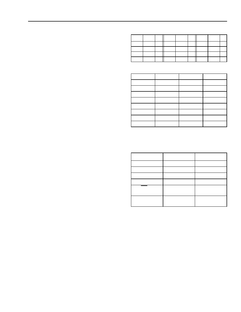
Table 2. Function Table for Qa, Qb, and Qc
Table 3. Function Table for QFB
1. If fselFB2 is set to 1, it may be necessary to apply a reset pulse after
powerup in order to ensure synchronization between the QFB and
other inputs.
Table 4. Function Table for Logic Selection
fsela1 fsela0 Qa fselb1 fselb0 Qb fselc1 fselc0 Qc
0
0
˜
4
0
0
˜
4
0
0
˜
2
0
1
˜
6
0
1
˜
6
0
1
˜
4
1
0
˜
8
1
0
˜
8
1
0
˜
6
1
1
˜
12
1
1
˜
10
1
1
˜
8
fselFB2
1
fselFB1
fselFB0
QFB
0
0
0
˜
4
0
0
1
˜
6
0
1
0
˜
8
0
1
1
˜
10
1
0
0
˜
8
1
0
1
˜
12
1
1
0
˜
16
1
1
1
˜
20
Control Pin
Logic 0
Logic 1
VCO_Sel
VCO/2
VCO
Ref_Sel
TCLK
Xtal (PECL)
TCLK_Sel
TCLK0
TCLK1
PLL_EN
Bypass PLL
Enable PLL
MR/OE
Master Reset/
Output High-Z
Enable Outputs
Inv_Clk
Noninverted
Qc2, Qc3
Inverted Qc2,
Qc3

6
Agere Systems Inc.
Data Sheet
February 2003
Low-Voltage PLL Clock Driver
LCK4973
Functional Description
(continued)
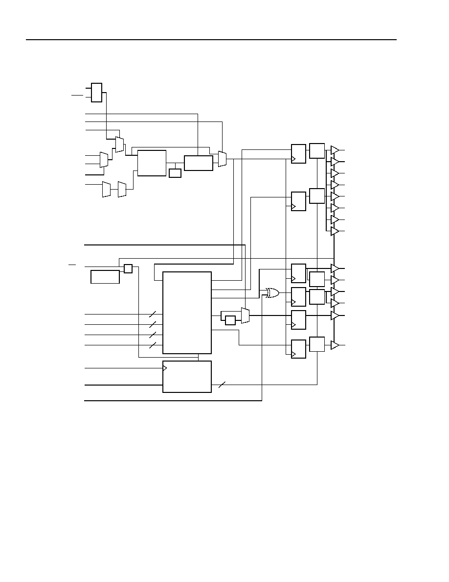
2332.a (F)
Figure 2. LCK4973 Logic Diagram
PCLK
PCLK
VCO_Sel
PLL_EN
REF_Sel
TCLK0
TCLK1
TCLK_Sel
Ext_FB
0
1
PHASE
DETECTOR
LPF
VCO
0
1
D Q
D Q
D Q
D Q
D Q
D Q
SYNC
Frz
SYNC
Frz
SYNC
Frz
SYNC
Frz
SYNC
Frz
Qa0
Qa1
Qa2
Qa3
Qb0
Qb1
Qb2
Qb3
Qc0
Qc1
Qc2
Qc3
QFB
QFB
QSync
0
1
˜
2
12
2
2
2
2
RESET
POWER-ON
˜
4,
˜
6,
˜
8,
˜
12
˜
4,
˜
6,
˜
8,
˜
10
˜
2,
˜
4,
˜
6,
˜
8
˜
4,
˜
6,
˜
8,
˜
10
SYNC PULSE
DATA
GENERATOR
OUTPUT DISABLE
CIRCUITRY
fselFB2
MR/OE
fsela0:1
fselb0:1
fselc0:1
fselFB0:1
Frz_Clk
Frz_Data
Inv_Clk

Agere Systems Inc.
7
Data Sheet
February 2003
Low-Voltage PLL Clock Driver
LCK4973
Functional Description
(continued)
Device Programming
The LCK4973 contains three independent banks of
four outputs as well as an independent PLL feedback
output. The possible configurations make Agere
Systems' LCK4973 one of the most versatile frequency
programming devices. Table 5 shows various selection
possibilities.
Table 5. Programmable Output Frequency
Relationships for Qa, Qb, and Qc
(VCO_Sel = 1)
Table 6. Programmable Output Frequency
Relationships for QFB (VCO_Sel = 1)
To determine the relationship between the three banks,
one would compare their divide ratios. For example, if
one desired a ratio of 5:3:2, set Qa to
˜
10, Qb to
˜
6,
and Qc to
˜
4. These selections would yield a 5:3:2
ratio.
For low frequency circumstances, the VCO_Sel pin
allows the option of an additional
˜
2 to be added to the
clock path. This pin maintains the output relationships,
but provides an extended clock range for the PLL. The
feedback output is matched to the input reference
frequency after the output frequency relationship is set
and VCO is in a stable range.
Only an external feedback is provided to the PLL in the
LCK4973 device to optimize flexibility. If, in the
previous example, the input reference frequency were
equal to the lowest output frequency, the output would
be set to
˜
10 mode. The fselFB2 input could be
asserted to half the frequency if the needed feedback
frequency is half of the lowest frequency output. This
multiplies the output frequencies by a factor of two,
relative to the input reference frequency.
Assume the previously mentioned 5:3:2 ratio, with the
highest output frequency of 100 MHz. If the only
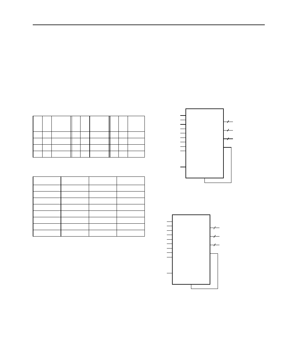
available reference frequency is 50 MHz, the setup of
Figure 3 can be used. The device provides 100 MHz,
66 MHz, and 40 MHz outputs, all generated from the
50 MHz source. Figure 4 and Figure 5 also show
possible configurations of the LCK4973.
2334.a (F)
Figure 3. 100 MHz from 50 MHz Example
2335.a (F)
Figure 4. Pentium Compatible Clocks Example
f
sel
a1
f
sel
a0
Qa
fs
e
l
b
1
fs
e
l
b
0
Qb
f
sel
c1
f
sel
c0
Qc
0
0
VCO/4
0
0
VCO/4
0
0 VCO/2
0
1
VCO/6
0
1
VCO/6
0
1 VCO/4
1
0
VCO/8
1
0
VCO/8
1
0 VCO/6
1
1 VCO/12 1
1 VCO/10 1
1 VCO/8
fselFB2
fselFB1
fselFB0
QFB
0
0
0
VCO/4
0
0
1
VCO/6
0
1
0
VCO/8
0
1
1
VCO/10
1
0
0
VCO/8
1
0
1
VCO/12
1
1
0
VCO/16
1
1
1
VCO/20
fsela0
fsela1
fselb0
fselb1
fselc0
fselc1
fselFB0
fselFB1
fselFB2
0
0
1
1
0
1
0
1
0
LCK4973
Qa
Qb
Qc
QFB
100 MHz
40 MHz
66.66 MHz
50 MHz
4
4
4
50 MHz
Input Ref
Ext_FB
VCO = 400 MHz
fsela0
fsela1
fselb0
fselb1
fselc0
fselc1
fselFB0
fselFB1
fselFB2
0
0
0
0
1
1
1
1
0
LCK4973
Qa
Qb
Qc
QFB
60 MHz (PROCESSOR)
60 MHz (PROCESSOR)
30 MHz (PCI)
24 MHz (FLOPPY DISK CLK)
4
4
4
24 MHz
Input Ref
Ext_FB

8
8
Agere Systems Inc.
Data Sheet
February 2003
Low-Voltage PLL Clock Driver
LCK4973
Functional Description
(continued)
Device Programming
(continued)
2336.a (F)
Figure 5. 20 MHz Source Example
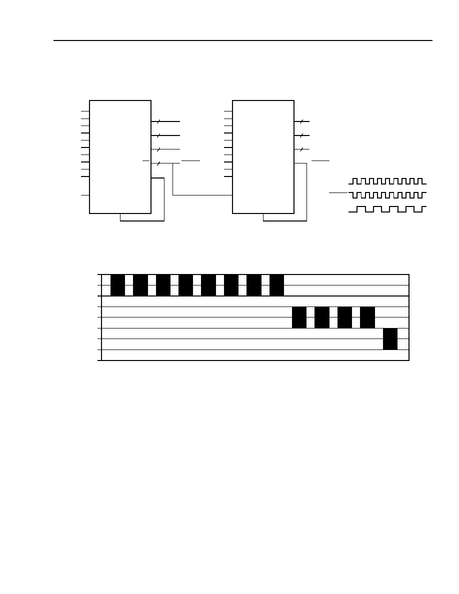
The Lnv_Clk input pin, when asserted, will invert the
Qc2 and Qc3 outputs.This inversion does not affect the
output-output skew of the device and allows for the
development of 180∞ phase-shifted clocks. This output
can also be used as a feedback output or routed to a
second PLL to generate early/late clocks. Figure 5 on
page 8 shows a 180∞ phase-shift configuration.
Zero-Delay Buffer Use
The LCK4973 can be used as a zero-delay buffer due
to the external feedback of the device. Using one of the
inputs as a feedback to the PLL eliminates the
propagation delay through the device. A near-zero
delay is produced by the PLL aligning to the output
edge to the input reference edge. The static phase
offset and the relative delay between the inputs and
outputs are affected by the reference frequency. This is
because the static phase offset is a function of the
reference clock and Tpd of the LCK4973 is a function
of the configuration used.
It is most likely that the LCK4973 will be used as a
zero-delay buffer in a nested clock-tree application. In
these instances, the LCK4973 offers a LVPECL clock
input as the PLL reference. This allows the user to
utilize the exceptional skew performance of the device
as the primary clock distribution device. The device can
then lock onto the LVPECL reference and translate,
with near-zero delay, to low-skew LVCMOS outputs.
These clock trees will show tighter skews than CMOS
fanout buffer clock trees.
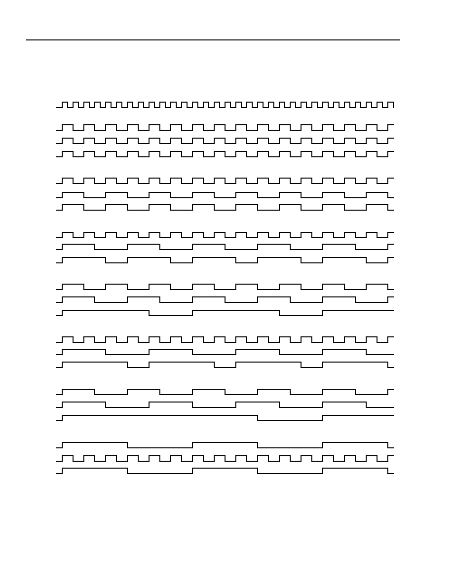
SYNC Output
When the output frequencies are not integer multiples
of each other, there is a need for a signal for
synchronization purposes. The SYNC output is
designed to address this need. The Qa and Qc banks
of outputs are monitored by the device, and a low-
going pulse (one period in duration, on period before
the coincident rising edges of Qa and Qc) is provided.
The duration and placement of the pulse is dependent
on the highest of Qa and Qc output frequencies. The
timing diagram, (Figure 8 on page 10) show the various
waveforms for SYNC.
Note: SYNC is defined for all possible combinations of
Qa and Qc, even though the lower frequency
clock should be used as a synchronizing signal
in most cases.
fsela0
fsela1
fselb0
fselb1
fselc0
fselc1
fselFB0
fselFB1
fselFB2
1
1
0
1
1
1
1
1
1
LCK4973
Qa
Qb
Qc
QFB
33 MHz (PCI)
50 MHz (PROCESSOR)
50 MHz (PROCESSOR)
20 MHz (ETHERNET)
4
4
4
20 MHz
Input Ref
Ext_FB

Agere Systems Inc.
9
Data Sheet
February 2003
Low-Voltage PLL Clock Driver
LCK4973
Functional Description
(continued)
SYNC Output
(continued)
2337.a (F)
Figure 6. Phase Delay Example Using Two LCK4973s
2338.a (F) r.1
Figure 7. Typical Skews Relative to QA
fsela0
fsela1
fselb0
fselb1
fselc0
fselc1
fselFB0
fselFB1
fselFB2
0
0
0
0
1
0
0
0
0
LCK4973
Qa
Qb
Qc
Qc
66 MHz
66 MHz
66 MHz
66 MHz
4
4
2
66 MHz
Input Ref
Ext_FB
Inv_Clk
1
fsela0
fsela1
fselb0
fselb1
fselc0
fselc1
fselFB0
fselFB1
fselFB2
0
1
0
1
1
1
0
0
0
LCK4973
Qa
Qb
Qc
QFB
33 MHz SHIFTED 90∞
33 MHz SHIFTED 90∞
33 MHz SHIFTED 90∞
66 MHz
4
4
4
Input Ref
Ext_FB
Inv_Clk
0
QFB
66 MHz
66 MHz
33 MHz
SHIFTED 90∞
2
≠100
≠75
≠50
≠25
0
25
50
75
100
Qc3
Qc2
Qc1
Qc0
Qb3
Qb2
Qb1
Qb0
Qa3
Qa2
Qa1
Qa0
ps
QFB

10
Agere Systems Inc.
Data Sheet
February 2003
Low-Voltage PLL Clock Driver
LCK4973
Functional Description
(continued)
SYNC Output
(continued)
2333.a (F)
Figure 8. LCK4973 Timing
fVCO
Qa
Qc
Sync
Qa
Qc
Sync
Qc(
˜
2)
Qa(
˜
6)
Sync
Qa(
˜
4)
Qc(
˜
6)
Sync
Qc(
˜
2)
Qa(
˜
8)
Sync
Qa(
˜
6)
Qc(
˜
8)
Sync
Qa(
˜
12)
Qc(
˜
2)
Sync
6:1 MODE
4:3 MODE
4:1 MODE
3:2 MODE
3:1 MODE
2:1 MODE
1:1 MODE

Agere Systems Inc.
11
Data Sheet
February 2003
Low-Voltage PLL Clock Driver
LCK4973
Functional Description
(continued)
Power Supply Filtering
The LCK4973 is a mixed-signal product which is
susceptible to random noise, especially when this
noise is on the power supply pins. To isolate the output
buffer switching from the internal phase-locked loop,
the LCK4973 provides separate power supplies for the
internal PLL (V
DDA
) and for the output buffers (V
DDO
).
In a digital system environment, besides this isolation
technique, it is highly recommended that both V
DDA
and V
DD
power supplies be filtered to reduce the
random noise as much as possible.
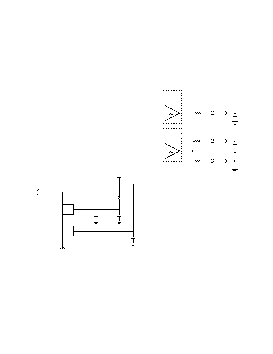
Figure 9 illustrates a typical power supply filter
scheme. Due to its susceptibility to noise with spectral
content in this range, a filter for the LCK4973 should be
designed to target noise in the 100 kHz to 10 MHz
range. The RC filter in Figure 9 will provide a broad-
band filter with approximately 100:1 attenuation for
noise with spectral content above 20 kHz. More elabo-
rate power supply schemes may be used to achieve
increased power supply noise filtering.
2344.a (F)
Figure 9. Power Supply Filter
Driving Transmission Lines
The output drivers of the LCK4973 were designed for
the lowest impedance possible for maximum flexibility.
The LCK4973's 10
impedance, the drivers can
accommodate either parallel or series terminated
transmission lines.
Point-to-point distribution of signals is the preferred
method in today's high-performance clock networks.
Series-terminated or parallel-terminated lines can be
used in a point-to-point scheme. The parallel
configuration terminates the signal at the end of the
line with a 50
resistance to V
DD
/2. Only one
terminated line can be driven by each output of the
LCK4973 due to the high level of dc current drawn.
In a series-terminated case, there is no dc current
draw, and the outputs can drive multiple series-termi-
nated lines. Figure 10 shows these scenarios.
2340.a (F)
Figure 10. Dual Transmission Lines
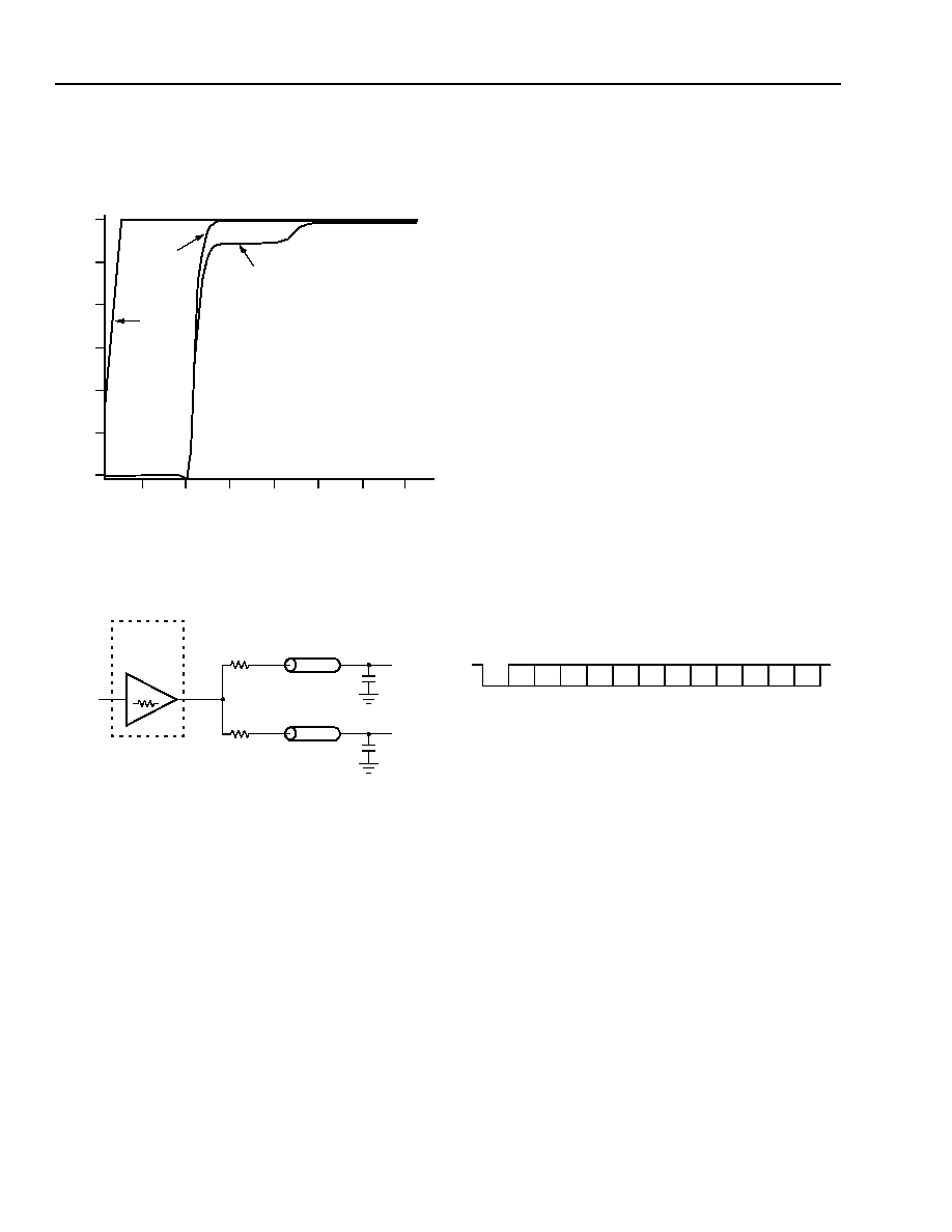
The waveform plots of Figure 11 show the simulated
results of a single output versus a two-line output. A
43 ps delta exists between the two differently loaded
outputs that can be seen in Figure 11. This implies that
dual-line driving need not be used in order to maintain
tight output-to-output skew. The step in Figure 11
shows an impedance mismatch caused when looking
into the driver. The parallel combination in Figure 10
plus the output resistance does not equal the parallel
combination of the line impedances. The voltage wave
down the lines will equal the following:
VL = VS (Z
0
/R
S
+ R
0
+ Z
0
) = 3.0 (25/53.5) = 1.4 V
The voltage will double at the load-end to 2.8 V, due to
the near-unity reflection coefficient. It then continues to
increment towards 3.0 V in one-round trip delay steps
(4 ps). This step will not cause any false clock
triggering, but some may not want these reflections on
the line. Figure 12 shows a possible configuration in
order to eliminate these reflections. In this scenario, the
series terminating resistors are reduced so the line
impedance is matched when the parallel combination is
added to the output buffer.
0.01
µ
F
22
µ
F
R
S
= 5
--10
V
DD
V
DDA
LCK4973
0.01
µ
F
3.3 V
Z
O
= 50
R
S
= 43
7
LCK4973
OUTPUT
BUFFER
IN
Z
O
= 50
R
S
= 43
7
LCK4973
OUTPUT
BUFFER
IN
Z
O
= 50
R
S
= 43
OUTA
OUTB0
OUTB1

12
12
Agere Systems Inc.
Data Sheet
February 2003
Low-Voltage PLL Clock Driver
LCK4973
Functional Description
(continued)
Driving Transmission Lines
(continued)
2341.a (F)
Figure 11. Single vs. Dual Waveforms
2342.a (F)
Figure 12. Optimized Dual Transmission Lines
Output Freeze Circuitry
The new green classification for computers requires
unique power management. The LCK4973's individual
output enable control allows software to implement
unique power management. A serial interface was
created to eliminate individual output control at the cost
of one pin per output.
The freeze control logic provides a mechanism for the
LCK4973's clock inputs to be stopped in the logic 0
state.
The freeze mechanism allows serial loading of the
12-bit serial input register. this register contains one
programmable freeze enable bit for 12 of the 14 output
clocks. The Qc0 and QFB outputs cannot be frozen
with the serial port, which prevents possible lock-up
situations if there is an error in the serial input register.
The user can also program a freeze by writing 0 to the
respective freeze bit. Likewise, it can be
programmability unfrozen by writing a 1 to that same
bit.
Freeze logic cannot force a recently frozen clock to a
logic 0 state before the time which it would normally
transition to that state. The logic will only maintain the
frozen clock in logic 0. Similarly, the logic will not force
a recently frozen clock to logic 1 before the time it
would normally transition there. when the clock would
normally be in a logic 0 state, the logic re-enables the
unfrozen clock, eliminating the possibility of runt clock
pulses.
The user may write to the serial input register by
supplying a logic 0 start bit followed (serially) by
12 NRZ freeze bits through Frz_Data. The period of the
Frz_Clk signal equals the period of each Frz_Data bit.
The timing should be such that the LCK4973 is able to
sample each Frz_Data bit with the rising edge of the
Frz_Clk (free-running) signal.
2343.a (F)
Note: D0--D3: control bits for Qa0--Qa3, respectively.
D4--D7: control bits for Qb0--Qb3, respectively.
D8--D10: control bits for Qc1--Qc3, respectively.
D11: control bit for QSync.
Figure 13. Freeze Data Input Protocol
VO
L
T
AG
E
(
V
)
OUTB
t
D
= 3.9386
OUTA
t
D
= 3.8956
IN
3.0
2.5
2.0
1.5
1.0
0
2
4
6
8
10
12
14
0.5
TIME (ns)
Z
O
= 50
R
S
= 36
7
LCK4973
OUTPUT
BUFFER
Z
O
= 50
R
S
= 36
7
+
36
36
= 50
50
25
= 25
D0
D1
D2
D3
D4
D5
D6
D7
D8
D10
D11
D9
START
BIT

Agere Systems Inc.
13
Data Sheet
February 2003
Low-Voltage PLL Clock Driver
LCK4973
Absolute Maximum Ratings
Stresses which exceed the absolute maximum ratings can cause permanent damage to the device. These are
absolute stress ratings only. Functional operation of the device is not implied at these or any other conditions in
excess of those given in the operational sections of the data sheet. Exposure to absolute maximum ratings for
extended periods of time can adversely affect device reliability.
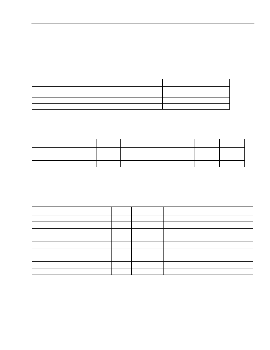
Table 7. Absolute Maximum Ratings
Electrical Characteristics
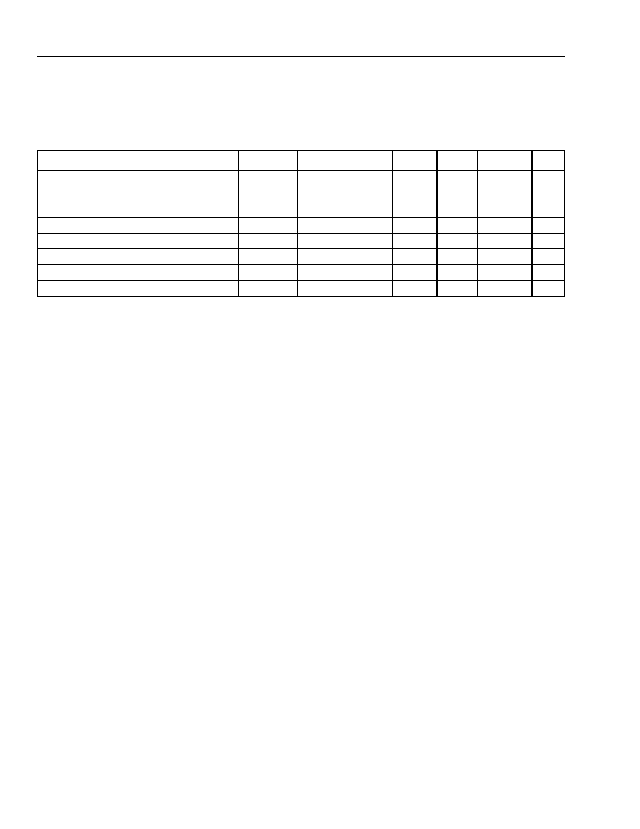
Table 8. PLL Input Reference Characteristics (T
A
= ≠40 ∞C to 85 ∞C)
1. Maximum input reference frequency is limited by VCO lock range and the feedback driver or 100 MHz. Minimum input reference fre-
quency is limited by the VCO lock range and the feedback divider.
dc Characteristics
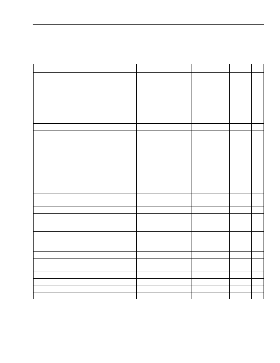
Table 9. dc Characteristics (T
A
= ≠40 ∞C to 85 ∞C, V
DD
= 3.3 V
±
5%)
1. The LCK4973 inputs can drive series of parallel terminated transmission lines on the incident edge.
2. Inputs have pull-up/pull-down resistors which affect input current.
3. Qa = Qb = Qc = 50 MHz, unoladed outputs.
Parameter
Symbol
Min
Max
Unit
Supply Voltage
V
DD
≠0.3
4.6
V
Input Voltage
V
I
≠0.3
V
DD
+ 0.3
V
Input Current
I
IN
--
±
20
mA
Storage Temperature Range
T
stg
≠40
125
∞C
Parameter
Symbol
Condition
Min
Max
Unit
TCLK Input Rise/Fall
tr, tf
--
--
3.0
ns
Reference Input Frequency
f
ref
--
--
1
--
1
MHz
Reference Input Duty Cycle
t
refDC
--
25
75
%
Parameter
Symbol
Condition
Min
Typ
Max
Unit
Input High Voltage
V
IH
--
2.0
--
3.6
V
Input Low Voltage
V
IL
--
--
--
0.8
V
Output High Voltage
V
OH
I
OH
= ≠20 mA
1
2.4
--
--
V
Output Low Voltage
V
OL
I
OL
= 20 mA
1
--
--
0.5
V
Input Current
I
IN
--
2
--
--
±
120
µ
A
Maximum Supply Current
I
DD
All V
DD
pins
--
130
160
mA
Analog V
DD
Current
I
DDA
V
DD
A pin only
3
--
60
85
mA
Input Capacitance
C
IN
--
--
--
4
pF
Power Dissipation Capacitance
C
pd
Per output
--
25
--
pF

14
Agere Systems Inc.
Data Sheet
February 2003
Low-Voltage PLL Clock Driver
LCK4973
Electrical Characteristics
(continued)
dc Characteristics
(continued)
Table 10. dc Characteristics (T
A
= ≠40 ∞C to 85 ∞C, V
DD
= 2.5 V
±
5%)
1. V
CMR(dc)
is the crosspoint of the differential input signal. Functional operation is obtained when the crosspoint is within the V
CMR
range and
the input swing lies within the V
p-p(dc)
specification.
2. The LCK4973 is capable of driving 50
transmission lines on the incident edge. Each output drives one 50
parallel terminated transmission
line to a termination voltage of V
TT
. Alternatively, the device drives up to two 50
series terminated transmission lines
.
3. Qa = Qb = Qc = 50 MHz, unoladed outputs.
Parameter
Symbol
Condition
Min
Typ
Max
Unit
PLL Supply Voltage
V
DD_PLL
LVCMOS
2.325
--
V
DD
V
Input High Voltage
V
IH
LVCMOS
1.7
--
V
DD
+ 0.3
V
Input Low Voltage
V
IL
LVCMOS
≠0.3
--
0.7
V
Output High Voltage
V
OH
I
OH
= ≠15 mA
2
1.8
--
--
V
Output Low Voltage
V
OL
I
OL
= 15 mA
--
--
0.6
V
Input Current
I
IN
V
IN
= V
DD
or GND
--
--
±
120
µA
Analog V
DD
Current
I
DDA
V
DDA
Pin Only
3
--
60
85
mA
Maximum Supply Current
I
DD
All V
DD
Pins
--
130
160
mA

Agere Systems Inc.
15
Data Sheet
February 2003
Low-Voltage PLL Clock Driver
LCK4973
Electrical Characteristics
(continued)
ac Characteristics
Table 11. ac Characteristics (T
A
= ≠40 ∞C to 85 ∞C, V
DD
= 3.3 V/2.5 V
±
5%)
1, 2
1. All ac characteristics are design targets and subject to change upon device characterization.
2. ac characteristics apply for parallel output termination of 50
to V
TT
.
3. In bypass mode, the LCK4973 divides the input reference clock.
4. The input reference frequency must match the VCO lock range divided be the total feedback divider ratio: f
REF
= f
VCO
˜
(M x VCO
_SEL
).
5. V
CMR(ac)
is the crosspoint of the differential input signal. Normal ac operation is obtained when the crosspoint is within the V
CMR
range and
the input swing lies within the Vp-p
(ac)
or Vp-pVp-pVp-p impacts static phase offset t(
).
Parameter
Symbol
Condition
Min
Typ
Max
Unit
Input Reference Frequency:
˜
4 feedback
˜
6 feedback
˜
8 feedback
˜
10 feedback
˜
12 feedback
˜
16 feedback
˜
24 feedback
˜
32 feedback
f
REF
PLL locked
50.0
33.3
25.0
20.0
16.6
12.5
8.33
6.25
--
--
--
--
--
--
--
--
120.0
80.0
60.0
48.0
40.0
30.0
20.0
15.0
MHz
Input Reference Frequency in PLL Bypass Mode
3
f
REF
PLL bypass
--
--
TBD
MHz
VCO Frequency Range
4
f
VCO
--
150
--
500
MHz
Output Frequency:
˜
2 feedback
˜
4 feedback
˜
6 feedback
˜
8 feedback
˜
10 feedback
˜
12 feedback
˜
16 feedback
˜
20 feedback
˜
24 feedback
f
MAX
PLL locked
100.0
50.0
33.3
25.0
20.0
16.6
12.5
10.0
8.33
--
--
--
--
--
--
--
--
--
240.0
120.0
80.0
60.0
48.0
40.0
30.0
24.0
20.0
MHz
Serial Interface Clock Frequency
f
STOP_CLK
--
--
--
20
MHz
Reference Input Duty Cycle
f
REFDC
--
25
--
75
%
CCLKx Input Rise/Fall Time
t
R
, t
F
20% to 80%
--
--
1.0
ns
Propagation Delay (static phase offset)
CCLKx to FB_IN
PCLK to FB_IN
t(
)
PLL locked
--
--
±150
±150
--
--
ps
Output-to-Output Skew
t
SK(O)
--
--
--
250
ps
Output Duty Cycle
DC
--
47
50
53
%
Output Rise/Fall Time
t
R
, t
F
20% to 80%
0.1
--
1.0
ns
Output Disable Time
t
PLZ, HZ
--
--
--
8
ns
Output Enable Time
t
PZL, LZ
--
--
--
8
ns
Cycle-to-Cycle Jitter (RMS 1
)
t
JIT(CC)
--
--
--
±100
ps
Period Jitter (RMS 1
)
t
JIT(PER)
--
--
TBD
--
ps
I/O Phase Jitter (RMS 1
)
t
JIT(
)
--
--
TBD
--
ps
PLL Closed Loop Bandwidth
BW
--
--
--
TBD
kHz
Maximum PLL Lock Time
t
LOCK
--
--
10
--
ms

PowerPC is a registered trademark of International Business Machines Corporation.
Pentium is a registered trademark of Intel Corporation.
Copyright © 2003 Agere Systems Inc.
All Rights Reserved
February 2003
DS03-073LCK (Replaces DS03-015LCK)
Agere Systems Inc. reserves the right to make changes to the product(s) or information contained herein without notice. No liability is assumed as a result of their use or application.
Agere, Agere Systems, and the Agere logo are trademarks of Agere Systems Inc.
Data Sheet
February 2003
Low-Voltage PLL Clock Driver
LCK4973
For additional information, contact your Agere Systems Account Manager or the following:
INTERNET:
http://www.agere.com
E-MAIL:
docmaster@agere.com
N. AMERICA: Agere Systems Inc., Lehigh Valley Central Campus, Room 10A-301C, 1110 American Parkway NE, Allentown, PA 18109-9138
1-800-372-2447, FAX 610-712-4106 (In CANADA: 1-800-553-2448, FAX 610-712-4106)
ASIA:
Agere Systems Hong Kong Ltd., Suites 3201 & 3210-12, 32/F, Tower 2, The Gateway, Harbour City, Kowloon
Tel. (852) 3129-2000, FAX (852) 3129-2020
CHINA: (86) 21-5047-1212 (Shanghai), (86) 755-25881122 (Shenzhen)
JAPAN: (81) 3-5421-1600 (Tokyo), KOREA: (82) 2-767-1850 (Seoul), SINGAPORE: (65) 778-8833, TAIWAN: (886) 2-2725-5858 (Taipei)
EUROPE:
Tel. (44) 1344 296 400
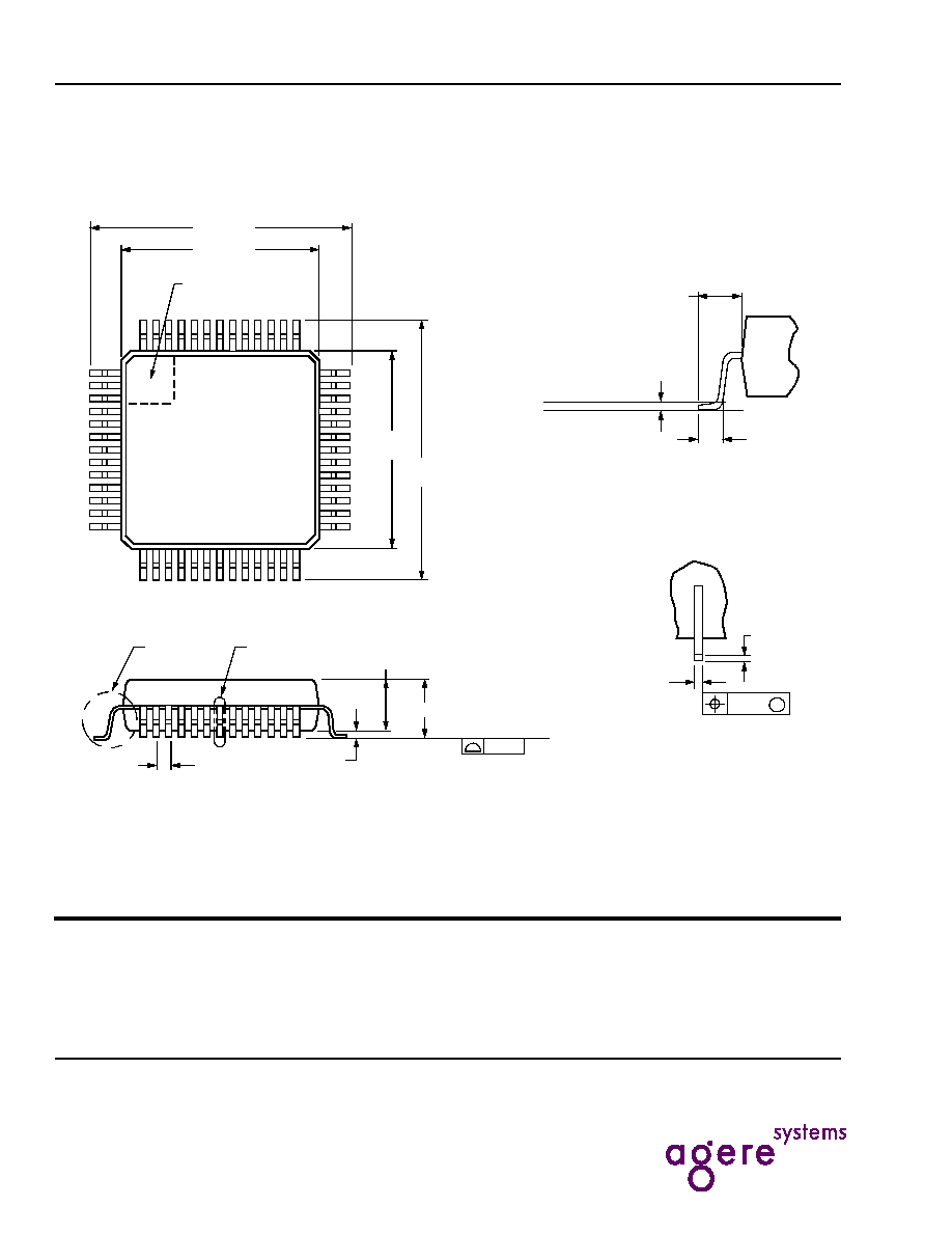
Outline Diagram
52-pin TQFPT package outline. All dimensions are in millimeters.
PIN #1
IDENTIFIER ZONE
26
10.00
1
52
40
13
14
39
27
12.00
1.20 MAX
SEATING PLANE
DETAIL A
0.08
1.00 ± 0.05
0.65 TYP
0.05/0.15
DETAIL B
DETAIL B
0.22/0.38
0.08
M
0.09/0.20
DETAIL A
0.45/0.75
GAGE PLANE
SEATING PLANE
1.00 REF
0.25
12.00
10.00

