
Data Sheet, Revision 1
May 5, 2004
LCK4993/LCK4994
Low-Voltage PLL Clock Drivers
1 Features
s
12 MHz--100 MHz (LCK4993), or 24 MHz--200 MHz
(LCK4994) output operation
s
Matched pair output skew <200 ps
s
Zero input-to-output delay
s
18 LVTTL 50% duty-cycle outputs capable of driving
50
terminated lines
s
3.3 V/2.5 V LVTTL/LV differential (LVPECL) fault tolerant
and hot insertable reference inputs
s
Phase adjustments from 625 ps up to 1300 ps steps up
to �10.4 ns
s
Output divide ratios of (1--6, 8, 10, 12)
s
Multiply ratios of (1--6, 8) x input frequency
s
Individual output bank disable for aggressive power
management and EMI reduction
s
Output high-impedance (HI-Z) option for testing
purposes
s
Fully integrated PLL with lock indicator
s
Single 3.3 V/2.5 V � 10% supply
s
100-pin TQFP package
s
100-ball FSBGA package
s
Pin-for-pin compatible with CYPRESS
�
CY7B993V and
CY7B994V
2 Description
The LCK4993 and LCK4994 low-voltage PLL clock drivers
offer user-selectable control over system clock functions.
The multiple-output clock drivers provide the system
integrator with functions necessary to optimize the timing of
high-performance computer and communication systems.
Each of the eighteen configurable outputs drive terminated
transmission lines with impedances as low as 50
while
delivering minimal and specified output skews at LVTTL
levels. The outputs are arranged in five banks. Banks 1--4
allow a divide function of 1 to 12, while simultaneously
allowing phase adjustments in 625 ps--1300 ps increments
up to 10.4 ns. One of the output banks also includes an
independent clock invert function. The feedback bank
consists of two outputs that allow divide-by functionality
from 1 to 12 and limited phase adjustments. Any one of
these eighteen outputs can be connected to the feedback
input or drive other inputs.
Selectable reference input is a fault tolerance feature that
allows smooth change over to the secondary clock source
when the primary clock source is not in operation. The
reference inputs and feedback inputs are configurable to
accommodate both LVTTL or differential (LVPECL) inputs.
The completely integrated PLL reduces jitter and simplifies
board layout.

LCK4993/LCK4994
Data Sheet, Revision 1
Low-Voltage PLL Clock Drivers
May 5, 2004
Table of Contents
Contents
Page
2
2
Agere Systems Inc.
1 Features .............................................................................................................................................................................1
2 Description ..........................................................................................................................................................................1
3 Functional Block Diagram ...................................................................................................................................................3
4 Pin Information ...................................................................................................................................................................4
4.1 100-Pin TQFP Diagram ...............................................................................................................................................4
4.2 Pin Descriptions ...........................................................................................................................................................5
5 Functional Description ........................................................................................................................................................7
5.1 Phase Frequency Detector and Filter ..........................................................................................................................7
5.2 VCO, Control Logic, Divider, and Phase Generator ....................................................................................................7
5.3 Time Unit Definition .....................................................................................................................................................7
5.4 Divide and Phase Select Matrix ...................................................................................................................................8
5.5 Timing Relationship of Programmable Skew Outputs .................................................................................................9
5.6 Output Disable Description ........................................................................................................................................10
5.7 INV3 Pin Function ......................................................................................................................................................10
5.8 Lock Detect Output Description .................................................................................................................................10
5.9 Factory Test Mode Description ..................................................................................................................................11
5.9.1 Factory Test Reset ...........................................................................................................................................11
5.10 Absolute Maximum Ratings .....................................................................................................................................11
5.11 Handling Precautions ..............................................................................................................................................12
5.12 Thermal Parameters (Definitions and Values) .........................................................................................................12
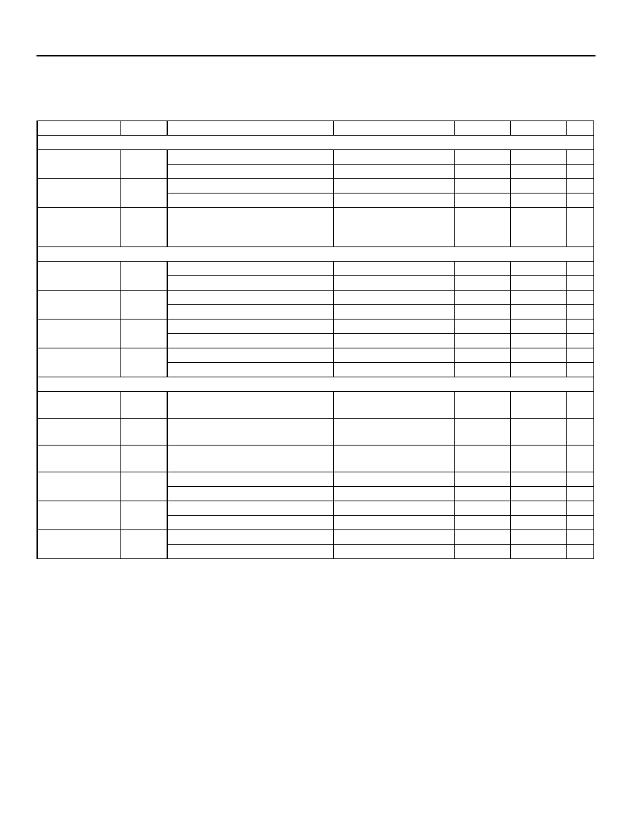
6 Electrical Characteristics ..................................................................................................................................................14
7 Timing ...............................................................................................................................................................................18
7.1 Switching Characteristics ..........................................................................................................................................18
7.2 ac Test Loads and Waveforms ..................................................................................................................................21
7.3 ac Timing Diagrams ...................................................................................................................................................22
8 Outline Diagrams ..............................................................................................................................................................23
8.1 100-Pin TQFP ............................................................................................................................................................23
8.2 100-Ball FSBGA ........................................................................................................................................................24
9 Ordering Information .........................................................................................................................................................25
Tables
Table 4-1. 100-Pin FSBGA Pin Assignments .........................................................................................................................4
Table 4-2. 100-Pin TQFP Descriptions ...................................................................................................................................5
Table 5-1. Frequency Range Select .......................................................................................................................................7
Table 5-2. N Factor Determination..........................................................................................................................................7
Table 5-3. Output Skew Select Function ................................................................................................................................8
Table 5-4. Output Divider Function .........................................................................................................................................8
Table 5-5. DIS[1:4]/FBDIS Pin Functionality.........................................................................................................................10
Table 5-6. Factory Test Mode Frequency Divide Select ....................................................................................................... 11
Table 5-7. Absolute Maximum Ratings ................................................................................................................................. 11
Table 5-8. Handling Precautions...........................................................................................................................................12
Table 5-9. Thermal Parameter Values ..................................................................................................................................13
Table 6-1. Electrical Characteristics (T
A
�40 �C to +85 �C, V
DD
= 3.3 V � 10%)..................................................................14
Table 6-2. Electrical Characteristics (T
A
�40 �C to +85 �C, V
DD
= 2.5 V � 10%)..................................................................16
Table 7-1. Switching Characteristics (T
A
�40 �C to +85 �C, V
DD
= 3.3 V � 10%).................................................................18
Table 7-2. Switching Characteristics (T
A
�40 �C to +85 �C, V
DD
= 2.5 V � 10%).................................................................20
Table 9-1. LCK4993 Ordering Information............................................................................................................................25
Table 9-2. LCK4994 Ordering Information............................................................................................................................25
Figures
Figure 3-1. LCK4993 and LCK4994 Functional Block Diagram .............................................................................................3
Figure 4-1. 100-Pin TQFP Package (Top View).....................................................................................................................4
Figure 5-1. Typical Outputs with FB Connected to a Zero-Skew Output................................................................................9
Figure 7-1. ac Test Loads and Waveforms ..........................................................................................................................21
Figure 7-2. ac Timing Diagrams ...........................................................................................................................................22
Data Sheet, Revision 1
LCK4993/LCK4994
May 5, 2004
Low-Voltage PLL Clock Drivers
Agere Systems Inc.
3
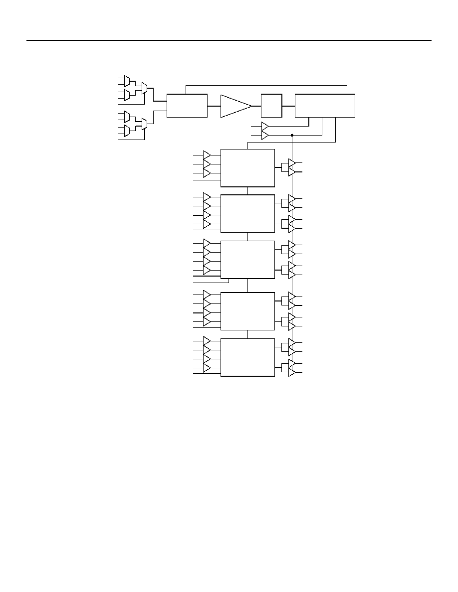
3 Functional Block Diagram
Figure 3-1. LCK4993 and LCK4994 Functional Block Diagram
DIVIDE AND
PHASE SELECT
MATRIX
3
3
3
3
1F0
1F1
1DS0
1DS1
DIS1
BANK 1
1QA0
1QA1
1QB0
1QB1
DIVIDE AND
PHASE SELECT
MATRIX
3
3
3
3
2F0
2F1
2DS0
2DS1
DIS2
BANK 2
2QA0
2QA1
2QB0
2QB1
DIVIDE AND
PHASE SELECT
MATRIX
3
3
3
3
3F0
3F1
3DS0
3DS1
DIS3
BANK 3
3QA0
3QA1
3QB0
3QB1
DIVIDE AND
PHASE SELECT
MATRIX
3
3
3
3
4F0
4F1
4DS0
4DS1
DIS4
BANK 4
4QA0
4QA1
4QB0
4QB1
3
3
3
FBF0
FBDS0
FBDS1
FBDIS
FEEDBACK BANK
QFA0
QFA1
DIVIDE AND
PHASE SELECT
MATRIX
3
3
OUTPUT_MODE
FS
PHASE
FREQUENCY
DETECTOR
CONTROL LOGIC
DIVIDE AND PHASE
GENERATOR
V
CO
FILTER
LOCK
REFB+
REFB�
REFSEL
REFA+
REFA�
FBKB+
FBKB�
FBSEL
FBKA+
FBKA�
INV3
LCK4993/LCK4994
Data Sheet, Revision 1
Low-Voltage PLL Clock Drivers
May 5, 2004
4
4
Agere Systems Inc.
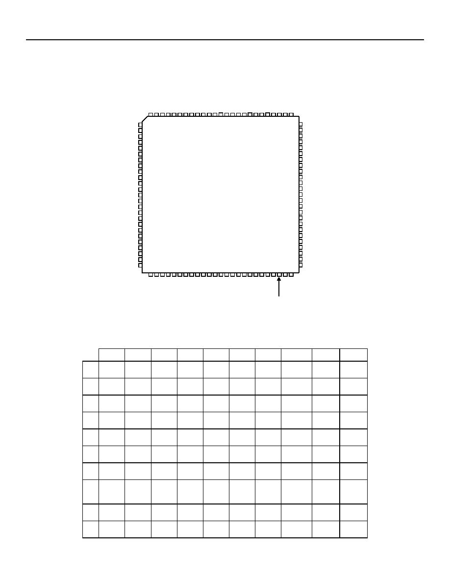
4 Pin Information
4.1 100-Pin
TQFP
Diagram
5-8885 (F) r.1
Figure 4-1. 100-Pin TQFP Package (Top View)
Table 4-1. 100-Pin FSBGA Pin Assignments
1
2
3
4
5
6
7
8
9
10
A
1QB1
1QB0
1QA1
1QA0
QFA0
QFA1
FBKB+
V
DD
Q
FBKA�
FBKA+
B
V
DDN
V
DDN
V
DDN
V
DDN
V
DDN
V
DDN
V
DDQ
FBKB�
FBSEL
REFA+
C
GND
GND
GND
GND
GND
GND
V
DD
Q
GND
GND
REFA�
D
LOCK
4F0
3F1
GND
FBDS1
FBDS0
2F0
V
DDQ
REFSEL
REFB�
E
4QB1
V
DDN
4DS1
GND
3F0
4F1
GND
FS
V
DDN
REFB+
F
4QB0
V
DDN
3DS1
GND
GND
GND
GND
FBF0
V
DDN
2QA0
G
4QA1
2DS1
V
DDQ
GND
GND
GND
GND
V
DDQ
1F0
2QA1
H
4QA0
1DS1
1DS0
V
DDQ
GND
GND
V
DDQ
OUTPUT_
MODE
FBDIS
2QB0
J
4DS0
3DS0
2DS0
DIS1
V
DDN
V
DDN
GND
INV3
DIS3
2QB1
K
2F1
1F1
DIS2
V
DDN
3QA0
3QA1
GND
3QB0
3QB1
DIS4
GND
V
DDQ
GND
1Q
A0
V
DDN
1Q
A1
GND
GND
V
DDN
1Q
B1
GND
FBD
S
0
FBD
S
1
LO
C
K
3F1
4F1
3F0
4F0
4DS1
3DS1
GND
4QB1
V
DDN
4QB0
GND
GND
4QA1
V
DDN
4QA0
GND
2DS1
1DS1
V
DDQ
4DS0
3DS0
2DS0
1DS0
GND
GN
D
GN
D
V
DDQ
V
DDQ
2F
1
1F
1
DI
S1
DI
S2
GN
D
3Q
A0
V
DDN
3Q
A1
GN
D
GN
D
3Q
B0
V
DDN
3Q
B1
GN
D
V
DDQ
INV
3
GN
D
OUTPUT_MODE
V
DDQ
REFA+
REFA�
REFSEL
REFB�
REFB+
2F0
FS
GND
2QA0
V
DDN
2QA1
GND
GND
2QB0
V
DDN
2QB1
GND
FBF0
1F0
GND
V
DDQ
FBDIS
DIS3
GND
QF
A0
V
DDN
QF
A1
GND
GND
FBKB+
FBKB�
FBSEL
FBKA�
FBKA+
V
DDQ
1Q
B0
88
89
90
91
92
93
95
96
97
98
99
10
0
87
86
85
84
83
82
81
80
79
78
77
76
94
38
37
36
35
34
33
31
30
29
28
27
26
39
40
41
42
43
44
45
46
47
48
49
50
32
13
12
11
10
9
8
6
5
4
3
2
1
14
15
16
17
18
19
20
21
22
23
24
25
7
63
64
65
66
67
68
70
71
72
73
74
75
62
61
60
59
58
57
56
55
54
53
52
51
69
DIS4
GN
D
GN
D
Data Sheet, Revision 1
LCK4993/LCK4994
May 5, 2004
Low-Voltage PLL Clock Drivers
Agere Systems Inc.
5
4.2 Pin Descriptions
For all 3-state inputs, low indicates a connection to GND, mid indicates an open connection, and high indicates a
connection to V
DD
. Internal termination circuitry holds an unconnected input to V
DD
/2.
Table 4-2. 100-Pin TQFP Descriptions
Pin
Symbol
Type
I/O
Description
1, 8, 12, 13, 17, 25--28,
35, 39, 40, 44, 47, 50,
55, 58, 62, 63, 67, 82,
83, 87, 88, 92, 93, 97
GND
Power
-- Ground.
2--5, 31, 32, 56, 69
[1:4]F[0:1]
3-Level
Input
I
Output Phase Function Select. Each pair controls the phase
function of the respective bank of outputs, see
Table 5-3
.
6, 7, 18, 19, 21--24
[1:4]DS[0:1]
3-Level
Input
I
Output Divider Function Select. Each pair controls the divide
function of the respective bank of outputs, see
Table 5-4
.
9, 11, 14, 16, 36, 38, 41,
43, 59, 61, 64, 66, 89,
91, 94, 96
[1:4]Q[A:B][0:1]
LVTTL
O Clock Output. These outputs provide numerous divide and
phase select functions determined by the [1:4]DS[0:1] and
[1:4]F[0:1] inputs.
10, 15, 37, 42, 60, 65,
85, 90, 95
V
DDN
Power
-- Output Buffer Power. Power supply for each output pair.
20, 29, 30, 45, 49, 54,
75, 76
V
DDQ
Power
-- Internal Power. Power supply for the internal circuitry.
33, 34, 51, 52
DIS[1:4]
LVTTL
I
d
Output Disable. Each input controls the state of the respective
output bank.
Low = the [1:4]Q[A:B][0:1] is enabled, see
Table 5-5
.
High = the output bank is disabled to the hold-off or HI-Z state;
the disable state is determined by OUTPUT_MODE.
46
INV3
3-Level
Input
I
Invert Mode. This input only affects Bank3.
Low = each matched output pair will become complementary
(3QA0+, 3QA1�, 3QB0+, 3QB1�).
Mid = all four outputs will be noninverting.
High = all four outputs in the same bank will be inverted.
48
OUTPUT_MODE 3-Level
Input
I
Output Mode. This pin determines the clock outputs' disable
state.
Low = the clock outputs will disable to hold-off mode.
Mid = the device enters factory test mode.
High = the clock outputs will disable to HI-Z.
53
FBDIS
LVTTL
I
d
Feedback Disable. This input controls the state of QFA[0:1].
Low = the QFA[0:1] is enabled, see
Table 5-5
.
High = the QFA[0:1] is disabled to the hold-off or HI-Z state; the
disable state is determined by OUTPUT_MODE.
57
FBF0
3-Level
Input
I
Feedback Output Phase Function Select. This input deter-
mines the phase function of the feedback banks QFA[0:1] out-
puts, see
Table 5-3
.
68
FS
3-Level
Input
I
Frequency Select. This input must be set according to the
nominal frequency (f
NOM
), see
Table 5-1
).
70, 71, 73, 74
REFB+, REFB�,
REFA�, REFA+
LVTTL/
LVDIFF
I
Reference Inputs. These inputs can operate as differential
PECL or single-ended TTL reference inputs to the PLL. When
operating as a single-ended LVTTL input, the complementary
input must be left open.
Note: I
d
= each input has an internal pull-down resistor.
LCK4993/LCK4994
Data Sheet, Revision 1
Low-Voltage PLL Clock Drivers
May 5, 2004
6
6
Agere Systems Inc.
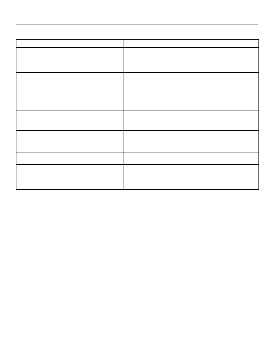
72
REFSEL
LVTTL
I
d
Reference Input Select. The REFSEL input controls how the
reference input is configured.
Low = REFSEL uses the REFA pair as the reference input.
High = REFSEL uses the REFB pair as the reference input.
77, 78, 80, 81
FBKA+, FBKA�,
FBKB�, FBKB+
LVTTL/
LVDIFF
I
Feedback Inputs. One pair of inputs selected by the FBSEL is
used to feedback the clock output xQn to the phase detector.
The PLL will operate so that the rising edges of the reference
and feedback signals are aligned in both phase and frequency.
These inputs can operate as differential PECL or single-ended
TTL inputs. When operating as a single-ended LVTTL input,
the complementary input must be left open.
79
FBSEL
LVTTL
I
d
Feedback Input Select.
Low = FBKA inputs are selected.
High = FBKB inputs are selected.
84, 86
QFA[0:1]
LVTTL
O Clock Feedback Output. This pair of clock outputs is intended
to be connected to the FB input. These outputs have numerous
divide options and three choices of phase adjustments. The
function is determined by setting the FBDS[0:1] pins and FBF0.
98, 99
FBDS[0:1]
3-Level
Input
I
Feedback Divider Function Select. These inputs determine
the function of the QFA0 and QFA1 outputs, see
Table 5-4
.
100
LOCK
LVTTL
O PLL Lock Indicator.
Low = the PLL is attempting to acquire lock.
High = this output indicates the internal PLL is locked to the ref-
erence signal.
Note: I
d
= each input has an internal pull-down resistor.
Table 4-2. 100-Pin TQFP Descriptions (continued)
Pin
Symbol
Type
I/O
Description
Data Sheet, Revision 1
LCK4993/LCK4994
May 5, 2004
Low-Voltage PLL Clock Drivers
Agere Systems Inc.
7
5 Functional Description
5.1 Phase Frequency Detector and Filter
These two blocks accept signals from the REF inputs (REFA+, REFA�, REFB+, or REFB�) and the FB inputs (FBKA+,
FBKA�, FBKB+, or FBKB�). Correction information is then generated to control the frequency of the voltage-controlled
oscillator (V
CO
). These two blocks, along with the V
CO
, form a phase-locked loop (PLL) that tracks the incoming REF
signal.
The devices have a flexible REF and FB input scheme. These inputs allow using either differential LVPECL or single-ended
LVTTL inputs. To configure as single-ended LVTTL inputs, the complementary input pin must be left open (internally pulled
to 1.5 V), and the other input pin can then be used as an LVTTL input. The REF inputs are also tolerant to hot insertion.
The REF inputs can be changed dynamically. When changing from one reference input to the other reference input of the
same frequency, the PLL is optimized to ensure that the clock output period will not be less than the calculated system
budget (t
MIN
= t
REF
(nominal reference clock period) � t
CCJ
(cycle-to-cycle jitter) � t
PDEV
(maximum period deviation)) while
reacquiring lock.
5.2 V
CO
, Control Logic, Divider, and Phase Generator
The V
CO
accepts analog control inputs from the PLL filter block. The FS control pin setting determines the nominal
operational frequency (f
NOM
) range of the divide-by-one output of the device. f
NOM
is directly related to the V
CO
frequency.
There are two versions of the device, a low-speed device (LCK4993) where f
NOM
ranges from 12 MHz to 100 MHz, and a
high-speed device (LCK4994) where f
NOM
ranges from 24 MHz to 200 MHz. The FS setting for each device is shown in
Table 5-1.
The f
NOM
frequency is seen on divide-by-one outputs. For the LCK4994, the upper f
NOM
range extends from 96 MHz to
200 MHz.
5.3 Time Unit Definition
Selectable skew is in discrete increments of time unit (t
U
). The value of t
U
is determined by the FS setting and the
f
NOM
frequency. The equation to be used to determine the t
U
is as follows:
(eq. 1)
Where N is a multiplication factor, determined by the FS setting and is defined in Table 5-2; where f
NOM
is the nominal
operating frequency of the VCO.
Table 5-1. Frequency Range Select
FS
*
* The level to be set on FS is determined by the f
NOM
of the V
CO
and phase generator. f
NOM
always appears on an output when the output is
operating in the divide by 1 mode. The REF and FB are at f
NOM
when the output connected to FB is in the divide by 1 mode.
LCK4993
LCK4994
f
NOM
(MHz)
f
NOM
(MHz)
Min
Max
Min
Max
Low
12
26
24
52
Mid
24
52
48
100
High
48
100
96
200
Table 5-2. N Factor Determination
FS
LCK4993
LCK4994
N
f
NOM
(MHz) at which t
U
= 1.0 ns
N
f
NOM
(MHz) at which t
U
= 1.0 ns
Low
64
15.265
32
31.25
Mid
32
31.25
16
62.5
High
16
62.5
8
125
t
U
1
f
NOM
N
�
--------------------------
=
LCK4993/LCK4994
Data Sheet, Revision 1
Low-Voltage PLL Clock Drivers
May 5, 2004
8
8
Agere Systems Inc.
5.4 Divide and Phase Select Matrix
The divide and phase select matrix is comprised of five independent banks as follows: four banks for clock outputs and one
bank for feedback. Each clock output bank has two pairs of low-skew, high-fanout output buffers ([1:4]Q[A:B][0:1]), two
phase function select inputs ([1:4]F[0:1]), two divider function selects ([1:4]DS[0:1]), and one output disable (DIS[1:4]).
The feedback bank has one pair of low-skew, high-fanout output buffers (QFA[0:1]). One of these outputs may connect to
the selected feedback input (FBK[A:B]�). This feedback bank also has one phase function select input (FBF0), two divider
function selects FSDS[0:1], and one output disable (FBDIS).
The phase capabilities that are chosen by the phase function select pins are shown in Table 5-3. The divide capabilities for
each bank are shown in Table 5-4.
Table 5-3. Output Skew Select Function
Function Selects
Output Skew Function
[1:4]F1
[1:4]F0 and FBF0
Bank1
Bank2
Bank3
Bank4
Feedback Bank
Low
Low
�4 t
U
�4 t
U
�8 t
U
�8 t
U
�4 t
U
Low
Mid
�3 t
U
�3 t
U
�7 t
U
�7 t
U
NA
Low
High
�2 t
U
�2 t
U
�6 t
U
�6 t
U
NA
Mid
Low
� 1t
U
�1 t
U
BK1
*
* BK1 denotes following the skew of Bank1.
BK2 denotes following the skew of Bank2.
BK1*
NA
Mid
Mid
0 t
U
0 t
U
0 t
U
0 t
U
0 t
U
Mid
High
1 t
U
1 t
U
BK2
BK2
NA
High
Low
2 t
U
2 t
U
6 t
U
6 t
U
NA
High
Mid
3 t
U
3 t
U
7 t
U
7 t
U
NA
High
High
4 t
U
4 t
U
8 t
U
8 t
U
4 t
U
Table 5-4. Output Divider Function
Function Selects*
Output Divider Function
[1:4]DS1 and FBDS1
[1:4]DS0 and FBDS0
Bank1
Bank2
Bank3
Bank4
Feedback Bank
Low
Low
/1
/1
/1
/1
/1
Low
Mid
/2
/2
/2
/2
/2
Low
High
/3
/3
/3
/3
/3
Mid
Low
/4
/4
/4
/4
/4
Mid
Mid
/5
/5
/5
/5
/5
Mid
High
/6
/6
/6
/6
/6
High
Low
/8
/8
/8
/8
/8
High
Mid
/10
/10
/10
/10
/10
High
High
/12
/12
/12
/12
/12
* Output frequency = f
NOM
(VCO frequency)/value of output divisor.
Data Sheet, Revision 1
LCK4993/LCK4994
May 5, 2004
Low-Voltage PLL Clock Drivers
Agere Systems Inc.
9
5.5 Timing Relationship of Programmable Skew Outputs
Figure 5-1 illustrates the timing relationship of programmable skew outputs. All times are measured with respect to REF,
with the output used for feedback programed with 0 t
U
skew. The PLL naturally aligns the rising edge of the FB input and
REF input. If the output used for feedback is programmed to another skew position, then the whole t
U
matrix will shift with
respect to REF. For example, if the output used for feedback is programmed to shift �8 t
U
, then the whole matrix is shifted
forward in time by 8 t
U
. Therefore, an output programed with 8 t
U
of skew will effectively be skewed 16 t
U
with respect to
REF.
Note: FB connected to an output selected for zero skew (i.e., FBF0 = mid or xF[1:0] = mid).
Figure 5-1. Typical Outputs with FB Connected to a Zero-Skew Output
1F[1:0]
2F[1:0]
3F[1:0]
4F[1:0]
NA
LL
�8 t
U
NA
LM
�7 t
U
NA
LH
�6 t
U
LL
NA
�4 t
U
LM
NA
�3 t
U
LH
NA
�2 t
U
ML
NA
�1 t
U
MM
MM
0 t
U
MH
NA
1 t
U
HL
NA
2 t
U
HM
NA
3 t
U
HH
NA
4 t
U
NA
HL
6 t
U
NA
HM
7 t
U
NA
HH
8 t
U
t
0
�
8 t
U
t
0
�
7 t
U
t
0
�
6 t
U
t
0
�
4 t
U
t
0
�
3 t
U
t
0
�
2 t
U
t
0
�
1 t
U
t
0
t
0
+ 1
t
U
t
0
+ 2
t
U
t
0
+ 3
t
U
t
0
+ 4
t
U
t
0
+ 5
t
U
t
0
+ 6
t
U
t
0
+ 7
t
U
t
0
+ 8
t
U
t
0
�
5 t
U
FB Input
REF Input
LCK4993/LCK4994
Data Sheet, Revision 1
Low-Voltage PLL Clock Drivers
May 5, 2004
10
10
Agere Systems Inc.
5.6 Output Disable Description
The feedback divide and phase select matrix bank has two outputs, each of the four divide and phase select matrix banks
have four outputs. The outputs of each bank can be independently put into a hold-off, or HI-Z state. The combination of the
OUTPUT_MODE and DIS[1:4]/FBDIS inputs determines the clock outputs' state for each bank. When the DIS[1:4]/FBDIS
is low, the outputs of the corresponding bank will be enabled. When the DIS[1:4]/FBDIS is high the outputs for that bank will
be disabled to a HI-Z or hold-off state, depending on the OUTPUT_MODE input. Table 5-5 defines the disabled output
functions.
The hold-off state is intended to be a power saving feature. An output bank is disabled to the hold-off state in a maximum of
six output clock cycles from the time when the disable input (DIS[1:4]/FBDIS) is high. When disabled to the hold-off state,
noninverting outputs are driven to a logic-low state on its falling edge. Inverting outputs are driven to a logic-high state on its
rising edge. This ensures the output clocks are stopped without a glitch. When a bank of outputs is disabled to a HI-Z state,
the respective bank of outputs will go HI-Z immediately.
5.7 INV3 Pin Function
Bank3 has signal invert capability. The four outputs of Bank3 will act as two pairs of complementary outputs when the INV3
pin is driven low. In complementary output mode, 3QA0 and 3QB0 are noninverting; 3QA1 and 3QB1 are inverting outputs.
All four outputs will be inverted when the INV3 pin is driven high. When the INV3 pin is left in mid, the outputs will not invert.
Inversion of the outputs are independent of the skew and divide functions. Therefore, clock outputs of Bank3 can be
inverted, divided, and skewed at the same time.
5.8 Lock Detect Output Description
The LOCK detect output indicates the lock condition of the integrated PLL. Lock detection is accomplished by comparing
the phase difference between the reference and feedback inputs. Phase error is declared when the phase difference
between the two inputs is greater than the specified device propagation delay limit (t
PD
).
When in the locked state, after four or more consecutive feedback clock cycles with phase-errors, the LOCK output will be
forced low to indicate out-of-lock state.
When in the out-of-lock state, 32 consecutive phase-errorless feedback clock cycles are required to allow the LOCK output
to indicate lock condition (LOCK = high).
If the feedback clock is removed after LOCK has gone high, a watchdog circuit is implemented to indicate the out-of-lock
condition after a time-out period by deasserting LOCK low. This time-out period is based on a divided down reference
clock. This assumes that there is activity on the selected REF input. If there is no activity on the selected REF input, then
the LOCK detect pin may not accurately reflect the state of the internal PLL.
Table 5-5. DIS[1:4]/FBDIS Pin Functionality
OUTPUT_MODE
DIS[1:4]/FBDIS
Output Mode
High/Low
Low
Enabled
High
High
HI-Z
Low
High
Hold-off
Mid
X
Factory Test

Data Sheet, Revision 1
LCK4993/LCK4994
May 5, 2004
Low-Voltage PLL Clock Drivers
Agere Systems Inc.
11
5.9 Factory Test Mode Description
The device will enter factory test mode when the OUTPUT_MODE input is driven to a mid level. In factory test mode, the
device will operate with its internal PLL disconnected. The reference input will replace the PLL output. While operating in
factory test mode, the selected FB input(s) must both be tied low. The output frequency is a function of the input level set on
the FS pin (see Table 5-6). When operating in factory test mode, all outputs must be set to the divide by 1 function. Output
skew select function operates normally, output bank disable is unavailable while operating in factory test mode. The
OUTPUT_MODE input is designed to be a static input. Dynamically toggling this input from low to high may temporarily
cause the device to go into factory test mode (when passing through the mid state).
5.9.1 Factory Test Reset
When operating in factory test mode (OUTPUT_MODE = mid), the device can be reset to a deterministic state by forcing
the DIS4 input to a logic high. With DIS4 in a logic high state, all clock outputs will go to HI-Z. After the selected reference
clock pin has five positive transitions, all the internal finite state machines (FSM) will be set to a deterministic state. The
deterministic state of the state machines will depend on the configuration of the divide select, skew select, and frequency
select inputs. All clock outputs will stay in high-impedance mode, and all FSMs will stay in the deterministic state until DIS4
is deasserted. When DIS4 is deasserted (with OUTPUT_MODE still at mid), the device will re-enter factory test mode.
5.10 Absolute Maximum Ratings
Stresses in excess of the absolute maximum ratings can cause permanent damage to the device. These are absolute
stress ratings only. Functional operation of the device is not implied at these or any other conditions in excess of those
given in the operational sections of the data sheet. Exposure to absolute maximum ratings for extended periods can
adversely affect device reliability.
Table 5-6. Factory Test Mode Frequency Divide Select
FS
LCK4993
LCK4994
Output Frequency
Output Frequency
Divide By
Divide By
Low
32
16
Mid
16
8
High
8
4
Table 5-7. Absolute Maximum Ratings
Parameter
Symbol
Min
Max
Unit
Storage Temperature
T
stg
�40
125
�C
Supply Voltage
V
DD
�0.5
4.6
V
dc Input Voltage
V
DC
�0.3
V
DD
+ 0.5
V
Output Current into Outputs (low)
I
OUT
--
40
mA
Latch-Up Current
I
L
--
�200
mA

LCK4993/LCK4994
Data Sheet, Revision 1
Low-Voltage PLL Clock Drivers
May 5, 2004
12
12
Agere Systems Inc.
5.11 Handling Precautions
Although electrostatic discharge (ESD) protection circuitry has been designed into this device, proper precautions must be
taken to avoid exposure to ESD and electrical overstress (EOS) during all handling, assembly, and test operations. Agere
employs both a human-body model (HBM) and a charged-device model (CDM) qualification requirement in order to deter-
mine ESD susceptibility limits and protection design evaluation. ESD voltage thresholds are dependent on the circuit
parameters used in each of the models, as defined by JEDEC's JESD22-A114 (HBM) and JESD22-C101 (CDM) stan-
dards.
Caution: MOS devices are susceptible to damage from electrostatic charge. Reasonable precautions in handling and pack-
aging MOS devices should be observed.
5.12 Thermal Parameters (Definitions and Values)
System and circuit board level performance depends not only on device electrical characteristics, but also on device thermal
characteristics. The thermal characteristics frequently determine the limits of circuit board or system performance, and they
can be a major cost adder or cost avoidance factor. When the die temperature is kept below 125 �C, temperature-activated
failure mechanisms are minimized. The thermal parameters that Agere provides for its packages help the chip and system
designer choose the best package for their applications, including allowing the system designer to thermally design and in-
tegrate their systems.
It should be noted that all the parameters listed below are affected, to varying degrees, by package design (including paddle
size) and choice of materials, the amount of copper in the test board or system board, and system airflow.
JA
- Junction to Air Thermal Resistance
JA
is a number used to express the thermal performance of a part under JEDEC standard natural convection conditions.
JA
is calculated using the following formula:
JA
= (T
J
� T
amb
) / P; where P = power
JMA
- Junction to Moving Air Thermal Resistance
JMA
is effectively identical to
JA
but represents performance of a part mounted on a JEDEC four-layer board inside a wind
tunnel with forced air convection.
JMA
is reported at airflows of 200 LFPM and 500 LFPM (linear feet per minute), which
roughly correspond to 1 m/s and 2.5 m/s (respectively).
JMA
is calculated using the following formula:
JMA
= (T
J
� T
amb
) / P
JC
- Junction to Case Thermal Resistance
JC
is the thermal resistance from junction to the top of the case. This number is determined by forcing nearly 100% of the
heat generated in the die out the top of the package by lowering the top case temperature. This is done by placing the top
of the package in contact with a copper slug kept at room temperature using a liquid refrigeration unit.
JC
is calculated using
the following formula:
JC
= (T
J
� T
C
) / P
Table 5-8. Handling Precautions
Device
Minimum Threshold
HBM
CDM
LCK4993
2000 V
500 V
LCK4994
2000 V
500 V

Data Sheet, Revision 1
LCK4993/LCK4994
May 5, 2004
Low-Voltage PLL Clock Drivers
Agere Systems Inc.
13
JB
- Junction to Board Thermal Resistance
JB
is the thermal resistance from junction to board. This number is determined by forcing the heat generated in the die out
of the package through the leads or balls by lowering the board temperature and insulating the package top. This is done
using a special fixture, which keeps the board in contact with a water chilled copper slug around the perimeter of the package
while insulating the package top.
JB
is calculated using the following formula:
JB
= (T
J
� T
B
) / P
JT
JT
correlates the junction temperature to the case temperature. It is generally used by the customer to infer the junction
temperature while the part is operating in their system. It is not considered a true thermal resistance.
JT
is calculated using
the following formula:
JT
= (T
J
� T
C
) / P
Table 5-9. Thermal Parameter Values
Parameter
Temperature �C/Watt
100-Pin TQFP
100-Ball FSBGA
JA
38
71.9
JMA
(1 m/s)
32.9
66.6
JMA
(2.5 m/s)
30.4
64.7
JC
32.9
24.5
JB
29.9
56.8
JT
1
1
LCK4993/LCK4994
Data Sheet, Revision 1
Low-Voltage PLL Clock Drivers
May 5, 2004
14
14
Agere Systems Inc.
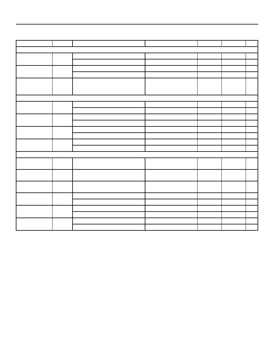
6 Electrical Characteristics
.
Table 6-1. Electrical Characteristics (T
A
�40 �C to +85 �C, V
DD
= 3.3 V � 10%)
Parameter
Symbol
Description
Test Conditions
Min
Max
Unit
LVTTL Compatible Output Pins (QFA[0:1], [1:4]Q[A:B], LOCK
High-Voltage
Output (LVTTL)
V
OH
QFA[0:1], [1:4]Q[A:B][0:1]
V
DD
= min, I
OH
= �30 mA
2.4
--
V
LOCK
V
DD
= min, I
OH
= �2 mA
2.4
--
V
Low-Voltage
Output (LVTTL)
V
OL
QFA[0:1], [1:4]Q[A:B][0:1]
V
DD
= min, I
OH
= 30 mA
--
0.5
V
LOCK
V
DD
= min, I
OH
= 2 mA
--
0.5
V
High-Imped-
ance State Leak-
age Current
I
OZ
--
--
�100
100
�A
LVTTL Compatible Pins (FBKA�, FBKB�, REFA�, REFB�, FBSEL, REFSEL, FBDIS, DIS[1:4])
High-Voltage
Input (LVTTL)
V
IH
FBK[A:B]�, REF[A:B]�
Min
V
DD
max
2.0
V
DD
+ 0.3
V
REFSEL, FBSEL, FBDIS, DIS[1:4]
--
2.0
V
DD
+ 0.3
V
Low-Voltage
Input (LVTTL)
V
IL
FBK[A:B]�, REF[A:B]�
Min
V
DD
max
�0.3
0.8
V
REFSEL, FBSEL, FBDIS, DIS[1:4]
--
�0.3
0.8
V
High-Input
Current (LVTTL)
I
IH
FBK[A:B]�, REF[A:B]�
V
DD
= max, V
IN
= V
DD
--
500
�A
REFSEL, FBSEL, FBDIS, DIS[1:4]
V
IN
= V
DD
--
500
�A
Low-Input
Current (LVTTL)
I
IL
FBK[A:B]�, REF[A:B]�
V
DD
= max, V
IN
= GND
�500
--
�A
REFSEL, FBSEL, FBDIS, DIS[1:4]
V
IN
= GND
�500
--
�A
3-Level Input Pins (FBF0, FBDS[0:1], [1:4]F[0:1], [1:4]DS[0:1], FS, OUTPUT_MODE(TEST)
Low-Voltage
3-Level Input
1
V
ILL
--
Min
V
DD
max
--
0.13 x V
DD
V
Mid-Voltage
3-Level Input
1
V
IMM
--
Min
V
DD
max
0.47 x V
DD
0.53 x V
DD
V
High-Voltage
3-Level Input
1
V
IHH
--
Min
V
DD
max
0.87 x V
DD
--
V
Low-Current
3-Level Input
I
ILL
3-level input pins excluding FBF0
V
IN
= GND
�200
--
�A
FBF0
V
IN
= GND
�400
--
�A
Mid-Current
3-Level Input
I
IMM
3-level input pins excluding FBF0
V
IN
= V
DD
/2
�50
50
�A
FBF0
V
IN
= V
DD
/2
�100
100
�A
High-Current
3-Level Input
I
IHH
3-level input pins excluding FBF0
V
IN
= V
DD
--
200
�A
FBF0
V
IN
= V
DD
--
400
�A
1. These inputs are normally wired to V
DD
, GND, or left unconnected (actual threshold voltages vary as a percentage of V
DD
). Internal termination
resistors hold the unconnected inputs at V
DD
/2. If these inputs are switched, the function and timing of the outputs may glitch and the PLL may
require an additional t
LOCK
time before all data sheet limits are achieved.

Data Sheet, Revision 1
LCK4993/LCK4994
May 5, 2004
Low-Voltage PLL Clock Drivers
Agere Systems Inc.
15
LVDIFF Input Pins (FBK[A:B]�, REF[A:B]�)
Input Differential
Voltage
V
DIFF
--
--
400
V
DD
mV
Lowest Input
Low Voltage
V
ILLP
--
--
GND
V
DD
� 0.4
V
Highest Input
High Voltage
V
IHHP
--
--
1.0
V
DD
V
Common-mode
Range (crossing
voltage)
V
COM
--
--
0.8
V
DD
V
Operating Current
Internal Operat-
ing Current
I
CCI
LCK4993
V
DD
= max, f
max
--
250
mA
LCK4994
V
DD
= max, f
max
1
--
250
mA
Output Current
Dissipation/Pair
2
I
CCN
LCK4993
V
DD
= max,
C
LOAD
= 25 pF,
R
LOAD
= 50
at
V
DD
/2, f
max
--
40
mA
LCK4994
V
DD
= max,
C
LOAD
= 25 pF,
R
LOAD
= 50
at
V
DD
/2, f
max
--
50
mA
Capacitance
Input Capaci-
tance
C
IN
--
T
A
= 25 �C, f = 1 MHz,
V
DD
= 3.3 V/2.5 V
--
5
pF
1. I
CCI
measurements are performed with Bank1 and FB bank configured to run at maximum frequency (f
NOM
= 100 MHz for LCK4993, f
NOM
=
200 MHz for LCK4994), and all other clock output banks to run at half the maximum frequency. FS and OUTPUT_MODE are asserted to the high
state.
2. This is dependent upon frequency and number of outputs of a bank being loaded. The value indicates maximum I
CCN
at maximum frequency and
maximum load of 25 pF terminated to 50
at V
DD
/2.
Table 6-1. Electrical Characteristics (T
A
�40 �C to +85 �C, V
DD
= 3.3 V � 10%) (continued)
Parameter
Symbol
Description
Test Conditions
Min
Max
Unit
LCK4993/LCK4994
Data Sheet, Revision 1
Low-Voltage PLL Clock Drivers
May 5, 2004
16
16
Agere Systems Inc.
Table 6-2. Electrical Characteristics (T
A
�40 �C to +85 �C, V
DD
= 2.5 V � 10%)
Parameter
Symbol
Description
Test Conditions
Min
Max
Unit
LVTTL Compatible Output Pins (QFA[0:1], [1:4]Q[A:B], LOCK)
High-Voltage
Output (LVTTL)
V
OH
QFA[0:1], [1:4]Q[A:B][0:1]
V
DD
= min, I
OH
= �30 mA
1.6
--
V
LOCK
V
DD
= min, I
OH
= �2 mA
1.6
--
V
Low-Voltage
Output (LVTTL)
V
OL
QFA[0:1], [1:4]Q[A:B][0:1]
V
DD
= min, I
OH
= 30 mA
--
0.5
V
LOCK
V
DD
= min, I
OH
= 2 mA
--
0.5
V
High-Imped-
ance State Leak-
age Current
I
OZ
--
--
�100
100
�A
LVTTL Compatible Pins (FBKA�, FBKB�, REFA�, REFB�, FBSEL, REFSEL, FBDIS, DIS[1:4])
High-Voltage
Input (LVTTL)
V
IH
FBK[A:B]�, REF[A:B]�
Min
V
DD
max
2.0
V
DD
+ 0.3
V
REFSEL, FBSEL, FBDIS, DIS[1:4]
--
2.0
V
DD
+ 0.3
V
Low-Voltage
Input (LVTTL)
V
IL
FBK[A:B]�, REF[A:B]�
Min
V
DD
max
�0.3
0.8
V
REFSEL, FBSEL, FBDIS, DIS[1:4]
--
�0.3
0.8
V
High-Input
Current (LVTTL)
I
IH
FBK[A:B]�, REF[A:B]�
V
DD
= max, V
IN
= V
DD
--
500
�A
REFSEL, FBSEL, FBDIS, DIS[1:4] V
IN
= V
DD
--
500
�A
Low-Input
Current (LVTTL)
I
IL
FBK[A:B]�, REF[A:B]�
V
DD
= max, V
IN
= GND
--
500
�A
REFSEL, FBSEL, FBDIS, DIS[1:4]
--
�500
--
�A
3-Level Input Pins (FBF0, FBDS[0:1], [1:4]F[0:1], [1:4]DS[0:1], FS, OUTPUT_MODE(TEST))
Low-Voltage
3-Level Input
1
V
ILL
--
Min
V
DD
max
--
0.13 x V
DD
V
Mid-Voltage
3-Level Input
1
V
IMM
--
Min
V
DD
max
0.47 x V
DD
0.53 x V
DD
V
High-Voltage
3-Level Input
1
V
IHH
--
Min
V
DD
max
0.87 x V
DD
--
V
Low-Current
3-Level Input
I
ILL
3-level input pins excluding FBF0
V
IN
= GND
�200
--
�A
FBF0
V
IN
= GND
�400
--
�A
Mid-Current
3-Level Input
I
IMM
3-level input pins excluding FBF0
V
IN
= V
DD
/2
�50
50
�A
FBF0
V
IN
= V
DD
/2
�100
100
�A
High-Current
3-Level Input
I
IHH
3-level input pins excluding FBF0
V
IN
= V
DD
--
200
�A
FBF0
V
IN
= V
DD
--
400
�A
1. These inputs are normally wired to V
DD
, GND, or left unconnected (actual threshold voltages vary as a percentage of V
DD
). Internal termination
resistors hold the unconnected inputs at V
DD
/2. If these inputs are switched, the function and timing of the outputs may glitch and the PLL may
require an additional t
LOCK
time before all data sheet limits are achieved.
Data Sheet, Revision 1
LCK4993/LCK4994
May 5, 2004
Low-Voltage PLL Clock Drivers
Agere Systems Inc.
17
LVDIFF Input Pins (FBK[A:B]�, REF[A:B]�)
Input Differential
Voltage
V
DIFF
--
--
400
V
DD
mV
Lowest Input
Low Voltage
V
ILLP
--
--
GND
V
DD
� 0.4
V
Highest Input
High Voltage
V
IHHP
--
--
1.0
V
DD
V
Common-mode
Range (crossing
voltage)
V
COM
--
--
0.8
V
DD
V
Operating Current
Internal Operat-
ing Current
I
CCI
LCK4993
V
DD
= max, f
max
--
250
mA
LCK4994
V
DD
= max, f
max
1
--
250
mA
Output Current
Dissipation/Pair
2
I
CCN
LCK4993
V
DD
= max,
C
LOAD
= 25 pF,
R
LOAD
= 50
at
V
DD
/2, f
max
--
40
mA
LCK4994
V
DD
= max,
C
LOAD
= 25 pF,
R
LOAD
= 50
at
V
DD
/2, f
max
--
50
mA
Capacitance
Input Capaci-
tance
C
IN
--
T
A
= 25 �C, f = 1 MHz,
V
DD
= 3.3 V/2.5 V
--
5
pF
1. I
CCI
measurements are performed with Bank1 and FB bank configured to run at maximum frequency (f
NOM
= 100 MHz for LCK4993, f
NOM
=
200 MHz for LCK4994), and all other clock output banks to run at half the maximum frequency. FS and OUTPUT_MODE are asserted to the high
state.
2. This is dependent upon frequency and number of outputs of a bank being loaded. The value indicates maximum I
CCN
at maximum frequency and
maximum load of 25 pF terminated to 50
at V
DD
/2.
Table 6-2. Electrical Characteristics (T
A
�40 �C to +85 �C, V
DD
= 2.5 V � 10%) (continued)
Parameter
Symbol
Description
Test Conditions
Min
Max
Unit
LCK4993/LCK4994
Data Sheet, Revision 1
Low-Voltage PLL Clock Drivers
May 5, 2004
18
18
Agere Systems Inc.
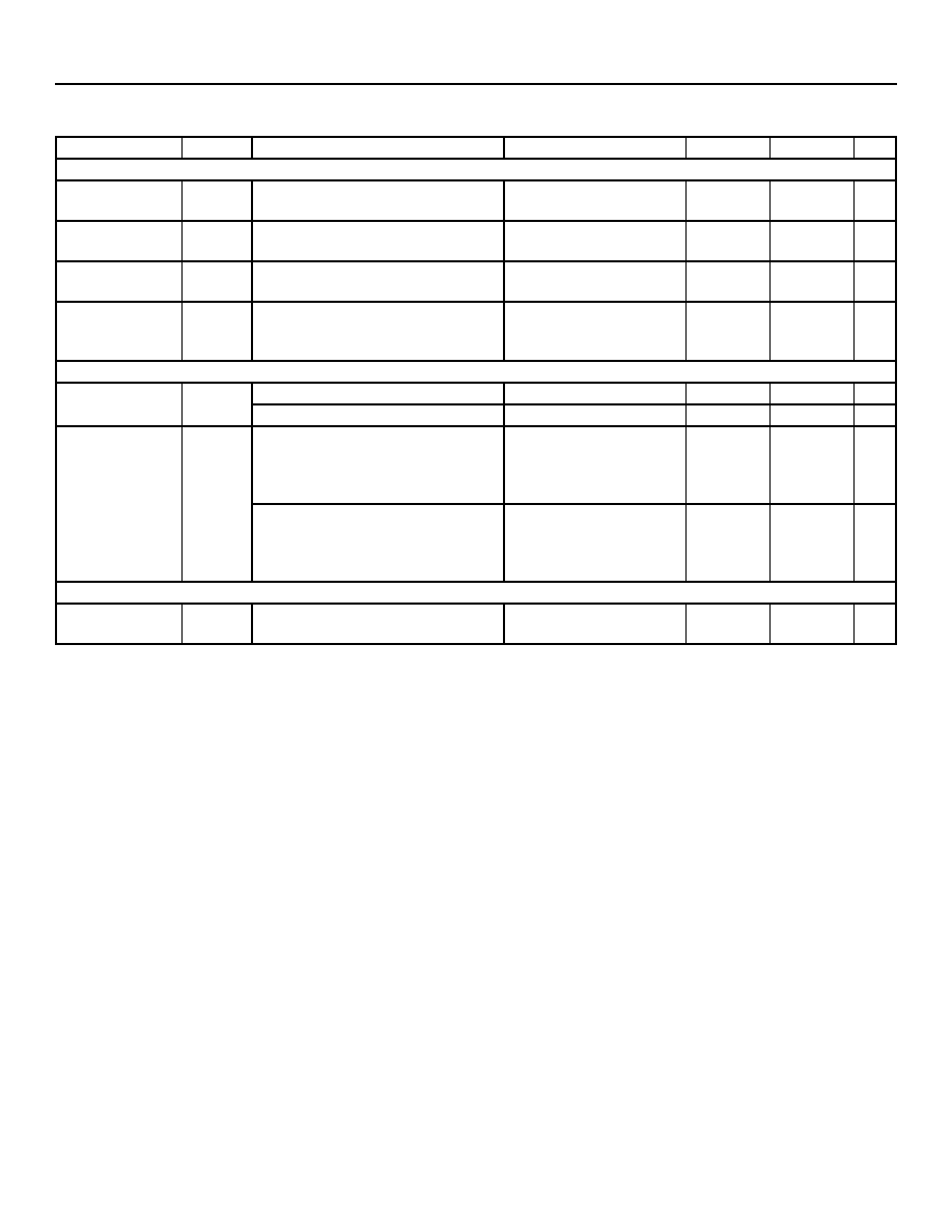
7 Timing
7.1 Switching Characteristics
The following switching characteristics and assumptions apply for non 3-level inputs.
s
A maximum 25 pF load capacitance is used for frequencies up to 185 MHz. A maximum 10 pF load capacitance is used
for
the frequency of 200 MHz.
s
Both outputs of the pair must be terminated, even if only one is being used.
s
ac parameters are measured at 50%, unless otherwise indicated.
Table 7-1. Switching Characteristics (T
A
�40 �C to +85 �C, V
DD
= 3.3 V � 10%)
Parameter
Symbol
Description
Min
Max
Unit
Clock Input Frequency
f
IN
LCK4993
12
100
MHz
LCK4994
24
200
MHz
Clock Output Frequency
f
OUT
LCK4993
12
100
MHz
LCK4994
24
200
MHz
REF Input
t
REFPWL
Pulse width low.
8
2.0
--
ns
t
REFPWH
Pulse width high.
8
2.0
--
ns
Matched-Pair Skew
1, 2
t
SKEWPR
Same frequency and phase, rise-to-rise and fall-to-
fall. (Matched pair outputs within a bank.)
1, 2
--
200
ps
Interbank Skew
t
SKEWBNK
Same frequency and phase, rise-to-rise and fall-to-
fall. (All outputs within a bank.)
1, 2
--
200
ps
Output-Output Skew
t
SKEW0
Same frequency and phase, rise-to-rise and fall-to-
fall. (All outputs across all banks.)
1, 2
--
250
ps
t
SKEW1
Different frequency same phase, rise-to-rise and
fall-to-fall. (All outputs all banks.)
1, 2
--
250
ps
t
SKEW2
Same frequency and phase, rise-to-fall and fall-to-
rise. (Bank 3 inverted to all other banks.)
1, 2, 3
--
250
ps
t
SKEW3
All output configurations outside t
SKEW1
and
t
SKEW2
.
1, 2
--
500
ps
Complementary
Outputs Skew
t
SKEWCPR
Crossing to crossing, complementary outputs.
(Bank 3 only.)
1, 2, 3, 4
--
200
ps
Cycle-to-Cycle Jitter
t
CCJ
Divide by 1 output frequency, FB = divide by 1--8
.
--
150
ps
Propagation Delay
t
PD
REF to FB rise.
�250
250
ps
t
PDDELTA
Difference between two devices.
4
--
200
ps
Output Rise/Fall Time
5
t
R
/t
F
--
0.15
2.0
ns
1. Test load C
L
maximum 25 pF (fnom
185 MHz) and maximum 10 pF (fnom = 200 MHz) both terminated 50
to V
DD
/2.
2. SKEW is defined as the time between the earliest and latest output transition among all outputs for which the same phase delay has been
selected and all outputs are equally loaded and properly terminated.
3. Complementary output skews are measured at complementary signal pair intersections.
4. Guaranteed by statistical correlation. Tested initially and after any design or process changes that may affect these parameters.
5. Rise and fall times are measured at 20% and 80% of the output voltage swing.
6. f
NOM
must be within the frequency range defined by the FS state (see Table 5-1).
7. ac parameters are measured at 50%, unless otherwise indicated.
8. t
PWL
is measured at 20%. t
PWH
is measured at 80%.
9. UI = unit interval. Examples: 1 UI is a full period. 0.1 UI is 10% of a period.
10. Measured at 0.5 V deviation from starting voltage.
11. For t
OZA
minimum, C
L
= 0 pF. For t
OZA
maximum, C
L
= 25 pF to 185 MHz or 10 pF at 200 MHz.
Data Sheet, Revision 1
LCK4993/LCK4994
May 5, 2004
Low-Voltage PLL Clock Drivers
Agere Systems Inc.
19
Parameter
Symbol
Description
Min
Max
Unit
PLL Lock Time from
Powerup
t
LOCK
--
--
10
ms
PLL Relock Time
t
RELOCK1
From same frequency, different phase, and with sta-
ble power supply.
--
500
�s
t
RELOCK2
From different frequency, different phase, and with
stable power supply.
6
--
1000
�s
Output Duty Cycle
7
t
ODCV
--
45
55
%
Period Deviation
t
PDEV
When changing from reference to reference.
--
0.025
UI
9
Output Disable Time
t
OZA
DIS[1:4]/FBDIS low to output active from output is
high-impedance.
10, 11
0.5
14
ns
Output Enable Time
t
OAZ
DIS[1:4]/FBDIS high to output high-impedance from
active.
1, 10
1.0
10
ns
1. Test load C
L
maximum 25 pF (fnom
185 MHz) and maximum 10 pF (fnom = 200 MHz) both terminated 50
to V
DD
/2.
2. SKEW is defined as the time between the earliest and latest output transition among all outputs for which the same phase delay has been
selected and all outputs are equally loaded and properly terminated.
3. Complementary output skews are measured at complementary signal pair intersections.
4. Guaranteed by statistical correlation. Tested initially and after any design or process changes that may affect these parameters.
5. Rise and fall times are measured at 20% and 80% of the output voltage swing.
6. f
NOM
must be within the frequency range defined by the FS state (see Table 5-1).
7. ac parameters are measured at 50%, unless otherwise indicated.
8. t
PWL
is measured at 20%. t
PWH
is measured at 80%.
9. UI = unit interval. Examples: 1 UI is a full period. 0.1 UI is 10% of a period.
10. Measured at 0.5 V deviation from starting voltage.
11. For t
OZA
minimum, C
L
= 0 pF. For t
OZA
maximum, C
L
= 25 pF to 185 MHz or 10 pF at 200 MHz.
Table 7-1. Switching Characteristics (T
A
�40 �C to +85 �C, V
DD
= 3.3 V � 10%) (continued)
LCK4993/LCK4994
Data Sheet, Revision 1
Low-Voltage PLL Clock Drivers
May 5, 2004
20
20
Agere Systems Inc.
Table 7-2. Switching Characteristics (T
A
�40 �C to +85 �C, V
DD
= 2.5 V � 10%)
Parameter
Symbol
Description
Min
Max
Unit
Clock Input Frequency
f
IN
LCK4993.
12
100
MHz
LCK4994.
24
200
MHz
Clock Output Frequency
f
OUT
LCK4993.
12
100
MHz
LCK4994.
24
200
MHz
REF Input
t
REFPWL
Pulse width low.
8
2.0
--
ns
t
REFPWH
Pulse width high.
8
2.0
--
ns
Matched-Pair Skew
1, 2
t
SKEWPR
Same frequency and phase, rise-to-rise and fall-to-
fall. (Matched pair outputs within a bank.)
1, 2
--
200
ps
Interbank Skew
t
SKEWBNK
Same frequency and phase, rise-to-rise and fall-to-
fall. (All outputs within a bank.)
1, 2
--
200
ps
Output-Output Skew
t
SKEW0
Same frequency and phase, rise-to-rise and fall-to-
fall. (All outputs across all banks.)
1, 2
--
250
ps
t
SKEW1
Different frequency same phase, rise-to-rise and
fall-to-fall. (All outputs all banks.)
1, 2
--
250
ps
t
SKEW2
Same frequency and phase, rise-to-fall and fall-to-
rise. (Bank 3 inverted to all other banks.)
1, 2, 3
--
250
ps
t
SKEW3
All output configurations outside t
SKEW1
and
t
SKEW2
.
1, 2
--
500
ps
Complementary Outputs
Skew
t
SKEWCPR
Crossing to crossing, complementary outputs.
(Bank 3 only.)
1, 2, 3, 4
--
200
ps
Cycle-to-Cycle Jitter
t
CCJ1--3
Divide by 1 output frequency, FB = divide by 1--8
.
--
150
ps
Propagation Delay
t
PD
REF to FB rise
.
�250
250
ps
t
PDDELTA
Difference between two devices.
4
--
200
ps
Output Rise/Fall Time
5
t
R
/t
F
--
0.15
2.0
ns
1. Test load C
L
maximum 25 pF (fnom
185 MHz) and maximum 10 pF (fnom = 200 MHz) both terminated 50
to V
DD
/2.
2. SKEW is defined as the time between the earliest and latest output transition among all outputs for which the same phase delay has been
selected and all outputs are equally loaded and properly terminated.
3. Complementary output skews are measured at complementary signal pair intersections.
4. Guaranteed by statistical correlation. Tested initially and after any design or process changes that may affect these parameters.
5. Rise and fall times are measured at 20% and 80% of the output voltage swing.
6. f
NOM
must be within the frequency range defined by the FS state (see Table 5-1).
7. ac parameters are measured at 50%, unless otherwise indicated.
8. t
PWL
is measured at 20%. t
PWH
is measured at 80%.
9. UI = unit interval. Examples: 1 UI is a full period. 0.1 UI is 10% of a period.
10. Measured at 0.5 V deviation from starting voltage.
11. For t
OZA
minimum, C
L
= 0 pF. For t
OZA
maximum, C
L
= 25 pF to 185 MHz or 10 pF at 200 MHz.
Data Sheet, Revision 1
LCK4993/LCK4994
May 5, 2004
Low-Voltage PLL Clock Drivers
Agere Systems Inc.
21
7.2 ac Test Loads and Waveforms
Note: Figure 7-1 is for illustrative purposes only. The actual ATE loads may vary.
Figure 7-1. ac Test Loads and Waveforms
Parameter
Symbol
Description
Min
Max
Unit
PLL Lock Time from
Powerup
t
LOCK
--
--
10
ms
PLL Relock Time
t
RELOCK1
From same frequency, different phase, and with
stable power supply.
--
500
�s
t
RELOCK2
From different frequency, different phase, and with
stable power supply.
6
--
1000
�s
Output Duty Cycle
7
t
ODCV
--
45
55
%
Period Deviation
t
PDEV
When changing from reference to reference.
--
0.025
UI
9
Output Disable Time
t
OZA
DIS[1:4]/FBDIS low to output active from output is
high-impedance.
10, 11
0.5
14
ns
Output Enable Time
t
OAZ
DIS[1:4]/FBDIS high to output high-impedance
from active.
1, 10
1.0
10
ns
1. Test load C
L
maximum 25 pF (fnom
185 MHz) and maximum 10 pF (fnom = 200 MHz) both terminated 50
to V
DD
/2.
2. SKEW is defined as the time between the earliest and latest output transition among all outputs for which the same phase delay has been
selected and all outputs are equally loaded and properly terminated.
3. Complementary output skews are measured at complementary signal pair intersections.
4. Guaranteed by statistical correlation. Tested initially and after any design or process changes that may affect these parameters.
5. Rise and fall times are measured at 20% and 80% of the output voltage swing.
6. f
NOM
must be within the frequency range defined by the FS state (see Table 5-1).
7. ac parameters are measured at 50%, unless otherwise indicated.
8. t
PWL
is measured at 20%. t
PWH
is measured at 80%.
9. UI = unit interval. Examples: 1 UI is a full period. 0.1 UI is 10% of a period.
10. Measured at 0.5 V deviation from starting voltage.
11. For t
OZA
minimum, C
L
= 0 pF. For t
OZA
maximum, C
L
= 25 pF to 185 MHz or 10 pF at 200 MHz.
Table 7-2. Switching Characteristics (T
A
�40 �C to +85 �C, V
DD
= 2.5 V � 10%) (continued)
0.8 V
2.0 V
3.3 V
0.8 V
2.0 V
GND
1 ns
1 ns
OUTPUT
3.3 V
R1
R2
C
L
TTL Input
LVTTL ac
Test Load
Test Waveform
s
For LOCK output only:
-- R1 = 910
-- R2 = 910
-- C
L
< 30 pF
s
For all other outputs:
-- R1 = 100
-- R2 = 100
-- C
L
max = 25 pF to 185 MHz
or C
L
max = 10 pF at 200 MHz
(The above include fixture and probe capacitances.)
TTL Input Waveform
LVTTL ac Test Load

LCK4993/LCK4994
Data Sheet, Revision 1
Low-Voltage PLL Clock Drivers
May 5, 2004
22
22
Agere Systems Inc.
7.3 ac Timing Diagrams
ac parameters are measured at 50%, unless otherwise indicated.
Figure 7-2. ac Timing Diagrams
REF
t
REFPWL
t
REFPWH
FB
Q
t
PD
t
PWH
t
PWL
80%
20%
t
CCJ1--3, 4--12
REF TO DEVICE 1 AND 2
FB DEVICE 1
FB DEVICE 2
t
PD
t
PDELTA
t
PDELTA
Q
INVERTED Q
t
SKEW2
t
SKEW2
Q
OTHER Q
t
SKEW0,1
t
SKEW0, 1
QFA0 OR
QFA1 OR
t
SKEWPR
t
SKEWPR
[1:4]Q[A:B]0
[1:4]Q[A:B]1
t
SKEWBNK
t
SKEWBNK
[1:4]QA[0:1]
[1:4]QB[0:1]
t
ODCV
t
ODCV
COMPLEMENTARY A
CROSSING
t
SKEWCPR
COMPLEMENTARY B
CROSSING
Data Sheet, Revision 1
LCK4993/LCK4994
May 5, 2004
Low-Voltage PLL Clock Drivers
Agere Systems Inc.
23
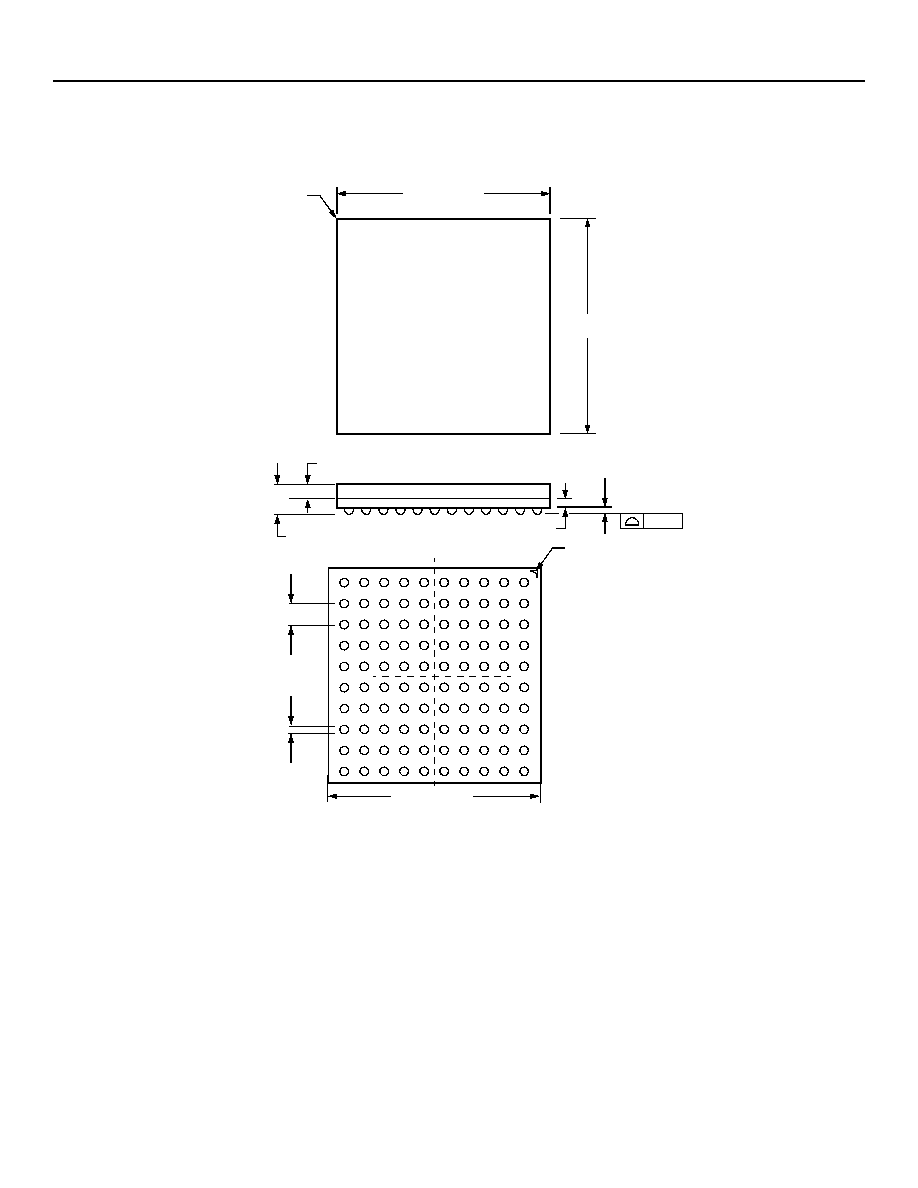
8 Outline Diagrams
8.1 100-Pin TQFP
Controlling dimensions are in millimeters.
5-2146 (F) r.1
0.50 TYP
1.60 MAX
SEATING PLANE
0.08
1.40
�
0.05
0.20 MAX
DETAIL A
DETAIL B
14.00
�
0.05
16.00
�
0.25
76
100
1
25
26
50
51
75
14.00
�
0.05
16.00
�
0.25
PIN #1 IDENTIFIER ZONE
DETAIL B
0.22 � 0.05
0.08
M
0.05/0.15
DETAIL A
0.45/0.75
GAGE PLANE
SEATING PLANE
1.00 REF
0.25
LCK4993/LCK4994
Data Sheet, Revision 1
Low-Voltage PLL Clock Drivers
May 5, 2004
24
24
Agere Systems Inc.
8.2 100-Ball FSBGA
Controlling dimensions are in millimeters.
5-8159.a (F) r.1
Note: The ball diameter, ball pitch, and stand-off and package thicknesses are different from JEDEC spec M0192 (low-pro-
file BGA family).
A
B
C
D
E
F
G
H
J
K
10
0.53
�
0.05
0.40
�
0.05
0.36
0.15
1.45 MAX
11.00
�
0.10
11.00
�
0.10
1.00
TYP
0.45
�
0.05
TYP 1.00
SOLDER BALLS
A1 INDICATOR
A1 INDICATOR
TOP VIEW
BOTTOM VIEW
11.00
�
0.10
8
7
6
5
4
3
2
1
9
Copyright � 2004 Agere Systems Inc.
All Rights Reserved
May 5, 2004
DS04-014LCK-1 (Replaces DS04-014LCK)
Agere Systems Inc. reserves the right to make changes to the product(s) or information contained herein without notice. No liability is assumed as a result of their use or application.
Agere is a registered trademark of Agere Systems Inc. Agere Systems and the Agere logo are trademarks of Agere Systems Inc.
For additional information, contact your Agere Systems Account Manager or the following:
INTERNET:
http://www.agere.com
E-MAIL:
docmaster@agere.com
N. AMERICA: Agere Systems Inc., Lehigh Valley Central Campus, Room 10A-301C, 1110 American Parkway NE, Allentown, PA 18109-9138
1-800-372-2447, FAX 610-712-4106 (In CANADA: 1-800-553-2448, FAX 610-712-4106)
ASIA:
Agere Systems Hong Kong Ltd., Suites 3201 & 3210-12, 32/F, Tower 2, The Gateway, Harbour City, Kowloon
Tel. (852) 3129-2000, FAX (852) 3129-2020
CHINA: (86) 21-54614688 (Shanghai), (86) 755-25881122 (Shenzhen)
JAPAN: (81) 3-5421-1600 (Tokyo), KOREA: (82) 2-767-1850 (Seoul), SINGAPORE: (65) 6778-8833, TAIWAN: (886) 2-2725-5858 (Taipei)
EUROPE:
Tel. (44) 1344 296 400
Data Sheet, Revision 1
LCK4993/LCK4994
May 5, 2004
Low-Voltage PLL Clock Drivers
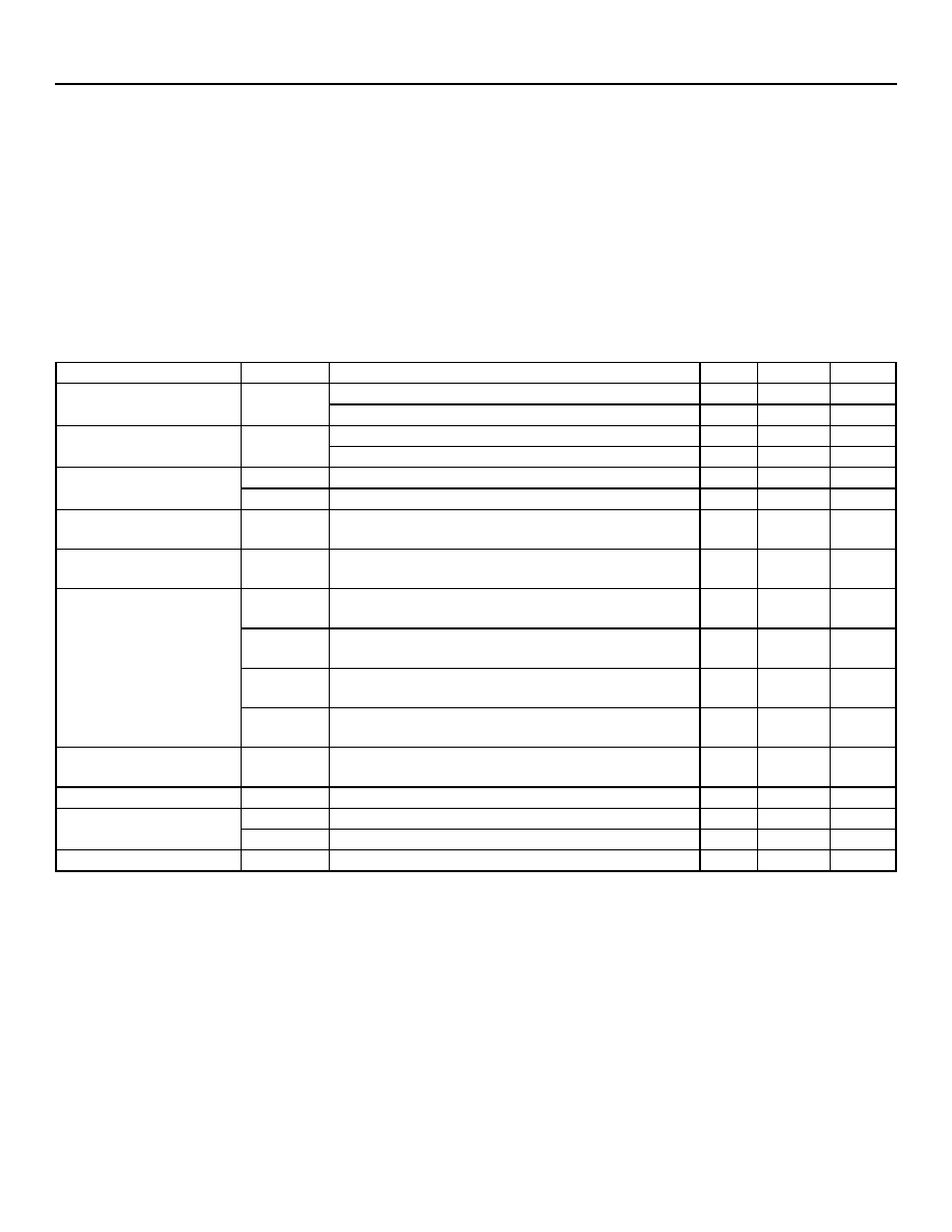
9 Ordering Information
Cypress is a registered trademark of Cypress Semiconductor Corporation.
Table 9-1. LCK4993 Ordering Information
Device
Package Type
Comcode
Delivery
LCK4993YH-DB
100FSBGA
700034618
Tray
LCK4993YH-DT
100FSBGA
700034619
Tape
LCK4993KB-DB
100TQFP
700024614
Tray
LCK4993KB-DT
100TQFP
700024615
Tape
Table 9-2. LCK4994 Ordering Information
Device
Package Type
Comcode
Delivery
LCK4994YH-DB
100FSBGA
700042835
Tray
LCK4994YH-DT
100FSBGA
700042836
Tape
LCK4994KB-DB
100TQFP
700025705
Tray
LCK4994KB-DT
100TQFP
700025708
Tape