Document Outline
- Features
- Applications
- Functional Description
- Theory of Operation
- Pin Information
- Absolute Maximum Ratings
- Recommended Operating Conditions
- Handling Precautions
- Mounting and Connections
- Electrical Characteristics
- Test Circuit
- Typical Performance Characteristics
- Outline Diagram
- 68-Pin Surface-Mount Package
- Ordering Information
- Appendix
- TF1004A Test Fixture Features
- Test Fixture Functional Description
- Before Use of Test Fixture
- Instructions for Use of Test Fixture
- List of Tables
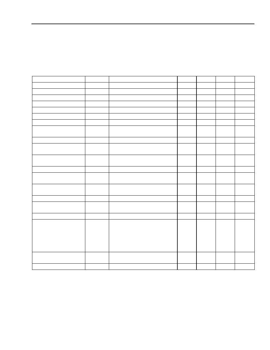
- Table 1. Pin Descriptions
- Table 2. Absolute Maximum Ratings
- Table 3. Recommended Operating Conditions
- Table 4. ESD Threshold
- List of Figures
- Figure 1. LG1600FXH Open View
- Figure 2. LG1600FXH Block Diagram
- Figure 3. Frequency and Phase Detector
- Figure 4. Timing Diagram
- Figure 5. Frequency and Phase Detector Characteristics
- Figure 6. Frequency Detector Operation
- Figure 7. Phase-Lock Loop Linear Model
- Figure 8. Jitter Bandwidth vs. External Resistor Value
- Figure 9. Pin Diagram
- Figure 10. LG1600FXH Typical Test Circuit
- Figure 11. LG1600FXH Typical Eye Patterns
- Figure 12. Data Clock Output Timing Diagram
- Figure 13. Error Recovery Timing Diagram
- Figure 14. Error Recovery Test Circuit
- Figure 15. TF1004A Test Fixture
- Figure 16. TF1004A Connector Assignment
- Contact Us
Data Sheet
August 1999
LG1600FXH Clock and Data Regenerator
Figure 1. LG1600FXH Open View
Features
s
Integrated clock recovery and data retiming
s
Surface-mount package
s
Single ECL supply
s
Robust FPLL design
s
Operation up to BER = 1e
≠3
s
SONET/SDH compatible loss of signal alarm
s
High effective Q allows long run lengths
s
Jitter tolerance exceeding ITU-T/Bellcore
s
Low clock jitter generation: typical <0.005 UI
s
Standard and custom data rates
0.50 Gbits/s--5.5 Gbits/s
s
Complementary 50
I/Os
Applications
s
SONET/SDH receiver terminals and regenerators
OC-12 through OC-96/STM-4 through STM-32
s
SONET/SDH test equipment
s
Proprietary bit rate systems
s
Digital video transmission
s
Clock doublers and quadruplers
Data Sheet
LG1600FXH Clock and Data Regenerator
August 1999
2
Lucent Technologies Inc.
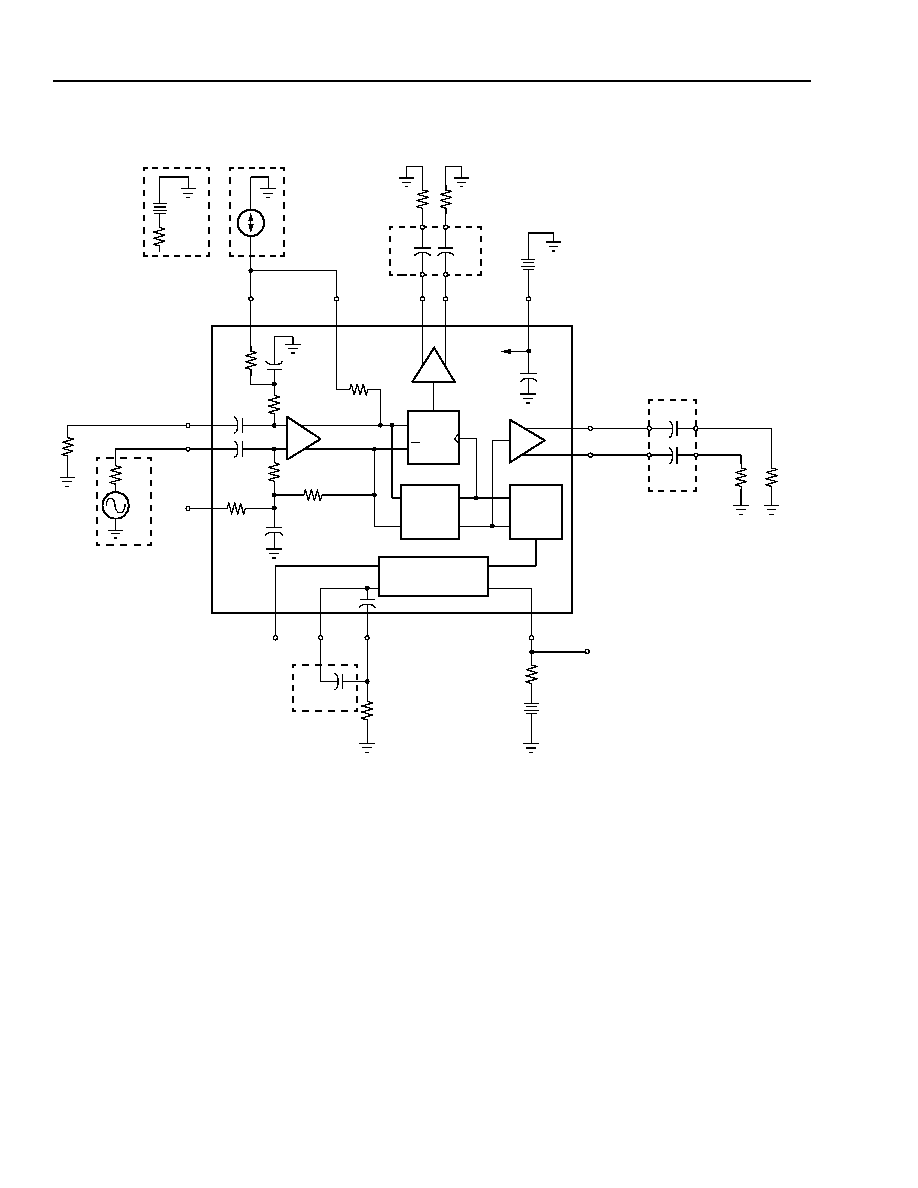
Functional Description
The LG1600FXH Clock and Data Regenerator (CDR)
is a compact, single device solution to clock recovery
and data retiming in high-speed communication sys-
tems such as fiber-optic data links and long-span fiber-
optic regenerators and terminals. Using frequency and
phase-lock loop (FPLL) techniques, the device regen-
erates clean clock and error-free data signals from a
nonreturn-to-zero (NRZ) data input, corrupted by jitter
and intersymbol interference. The LG1600FXH
exceeds ITU-T/Bellcore jitter tolerance requirements
for SONET/SDH systems.
The device houses two integrated circuits on an alu-
mina substrate inside a hermetically sealed 3 cm
◊
3 cm (1.2 in.
◊
1.2 in.) surface-mount package: a GaAs
IC that contains the high-speed part of an FPLL as well
as a highly sensitive decision circuit; and a silicon bipo-
lar IC that contains a loop filter, acquisition, and signal
detect circuitry.
The two ac-coupled complementary data inputs can be
driven differentially as well as single ended. A dc feed-
back voltage V
≠FB
maintains a data input threshold
V
≠TH
(decision level) that is optimum for a wide range
of 50% duty cycle input levels (connect to V
≠TH
). If
needed, the user can supply an external threshold to
compensate for different mark densities or distorted
input signals (see Figure 10).
Regenerated clock and data are available from comple-
mentary outputs that can either be ac coupled, to pro-
vide 50
output match, or dc coupled with 50
to
ground at the receiving end.
The second-order PLL filter bandwidth is set by the
user with an external resistor between pin 11 and
ground (required). An internal capacitor provides suffi-
cient PLL damping for most applications. In critical
applications, PLL damping can be increased using an
external capacitor between pins 9 and 11.
The device is powered by a single ≠5.2 V ECL compat-
ible supply and typically consumes 1.5 W.
The LG1600FXH comes in standard bit rates, but can
be factory tuned for any rate between 500 Mbits/s and
5500 Mbits/s.
A test fixture (TF1004A) with SMA connectors is avail-
able to allow quick evaluation of the LG1600FXH.
Theory of Operation
A digital regenerator has the task of retransmitting a bit
stream that is received from a remote source with the
same fidelity at which it was originally transmitted.
Two basic properties of the digital signal need to be
restored: the timing of the transitions between the bits
and the value of each bit.
12-3225(F)r.6
Figure 2. LG1600FXH Block Diagram
VCO
Q
D
V
+
CLKO
V
≠
CLKO
31
26
D
FREQ. &
90
∞
LOOP CONTROL &
11
9
7
V
REF
C
EXT
R
EXT
LOS
V
≠TH
51
V
≠FB
48
55
60
65
V
≠IN
V
+IN
V
+FB
0.047
µ
F
0.047
µ
F
0.047
µ
F
0.047
µ
F
1 k
50
25 k
50
25 k
1 k
43
38
V
+
OUT
V
≠
OUT
V
SS
35
0.047
µ
F
0.047
µ
F
SIGNAL DETECT
PHASE
DETECT.
0
∞
Data Sheet
August 1999
LG1600FXH Clock and Data Regenerator
3
Lucent Technologies Inc.
Theory of Operation
(continued)
Consequently, the timing information that is present in
the data needs to be extracted and a decision as to the
value of each bit must be made. Both timing instant and
decision levels are critical, since the economics of data
transmission dictate the largest distance possible
between transmitter and receiver. A practically closed
data eye can therefore be expected at the output of the
receiver, allowing only a small decision window.
An added complication in nonreturn-to-zero (NRZ) sys-
tems is the absence of clock component in the data
signal itself. Practical clock recovery circuits have used
a combination of nonlinear processing to extract a
spectral component at the clock frequency and narrow-
band filtering using a SAW filter or dielectric resonator.
The relative bandwidth of such a filter must be on the
order of a few tenths of a percent to minimize the data
pattern dependence of the resulting clock. Temperature
behavior of the passband characteristics, such as
group delay, must be tightly matched to that of the data
path. These extreme requirements make such a dis-
crete design very difficult to manufacture at Gbits/s
data rates.
The LG1600FXH clock and data regenerator relies on
phase-lock loop techniques, rather than passive filter-
ing. The filter properties of a PLL are determined at low
frequencies where parasitic elements play only a minor
roll and stability is easily maintained. Furthermore, the
reference frequency is determined by the data rate
itself, rather than by the physical properties of a band-
pass filter.
Although PLLs can eliminate some of the shortcomings
of passive bandpass filters used in clock recovery cir-
cuits, care was taken in the design of the LG1600FXH
to preserve desired properties such as linearity of the
jitter characteristics. A linear jitter transfer makes it a lot
easier for the system designer to predict the overall
performance of a link.
As a result, the architecture chosen for the device is not
basically different from the conventional clock recovery
circuit. A transition detector extracts a pulse train from
the incoming data signal which is used as a reference
signal for a PLL. The transition pulse train can be seen
as a clock signal that is modulated with the instanta-
neous transition density of the data signal. The PLL
locks onto the frequency and phase of this pulse train
and freewheels during times when transitions are
absent. The LG1600FXH features dual phase detec-
tors; one driven by an in-phase clock which is also driv-
ing the decision circuit flip-flop, the other is driven by a
quadrature clock. The phase detectors produce a zero
output when their respective clocks are centered with
respect to the transition pulses.
12-3226(F)r.3
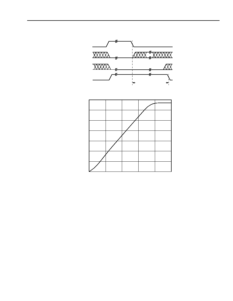
Figure 3. Frequency and Phase Detector
For a transition pulse of half the width of the bit period,
the timing diagram of Figure 4 shows how the in-phase
clock ends up in the center of the data eye when the
quadrature-phase detector output is forced to zero by
the loop. The (patented) transition detector is com-
prised of an (active) circulator, a shorted stub, and an
exclusive-OR gate. The circulator/stub combination
produces a delayed version of the data. A transition at
the input of the circuit results in an output pulse from
the exclusive-OR gate whose width equals the return
delay of the stub. The stub is tuned for a given bit rate
and can be adjusted so that the in-phase clock is
exactly centered in the error-free phase range of the
retiming flip-flop.
12-3227(F)r.2
Figure 4. Timing Diagram
PDQ
PDI
LOGIC
TO FLIP-FLOP
FROM
VCO
90
∞
0
∞
TRANSITION
PULSE
DATA
CIRCULATOR
DELAYED
DATA
STUB
FPD OUT
90
∞
0
∞
TRANSITION
DELAYED
DATA
1/2 T
1/4 T
DATA
PULSE
CLOCK
CLOCK
T
Data Sheet
LG1600FXH Clock and Data Regenerator
August 1999
4
Lucent Technologies Inc.
Theory of Operation
(continued)
12-3228(F)r.4
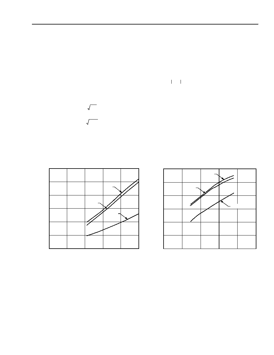
Figure 5. Frequency and Phase Detector
Characteristics
The frequency detector is not a separate function but
an integral part of the phase-lock loop. Any transition
between frequency and phase acquisition is completely
avoided. Figure 5 shows the output characteristics of
the FPD, which is essentially an extended range phase
detector. The two quadrature clock phases are used to
produce hysteresis, which extends the phase detector
range to ±270∞. The extended range gives the phase
detector a static frequency sensitivity as demonstrated
in Figure 6. For clock frequencies lower than the bit rate
(the phase is increasing), the top trajectory of the dia-
gram in Figure 6 is followed. When the VCO frequency
exceeds the bit rate, the lower trajectory applies. Since
the linear part of the phase detector produces a net-
zero output, in the first instance, positive pulses are fed
into the loop filter increasing the VCO frequency, while
in the latter case, the FPD produces negative pulses.
The wide, 540∞ range of the phase detector is also
responsible for the high jitter tolerance of the
LG1600FXH and an associated immunity to cycle slip
under high jitter conditions. The clock can be momen-
tarily misaligned as much as 270∞ but still return to its
original position. This property is extremely important
in synchronous systems, since a cycle slip would cause
misalignment of the demultiplexer following the circuit
resulting in a loss of frame condition. The LG1600FXH
can handle bit error rates up to 1e
≠3
as a result of low-
frequency jitter.
12-3229(F)r.4
Figure 6. Frequency Detector Operation
PLL Dimensioning
The LG1600FXH CDR employs a heavily damped
second order phase-lock loop. A linear model of this
PLL is depicted in Figure 7. The conventional second-
order equation describing the jitter transfer of the PLL
is shown below:
where
i
and
o
denote the input and output phase,
respectively,
is the PLL damping ratio and
n
is the
natural frequency. For most clock recovery applications
a very high damping is required, that renders the PLL
essentially as a first-order system with a slight peaking
that is generally undesirable. The second-order equa-
tion above does not provide much insight into the peak-
ing and bandwidth parameters.
12-3230(F)r.5
Figure 7. Phase-Lock Loop Linear Model
≠360
∞
≠180
∞
0
∞
180
∞
360
∞
FPD OUT
PHASE
FPD
OUT
FPD
OUT
TIME
TIME
A. fck < f
B
B. fck > f
B
H s
( )
o
i
------ s
( )
2
n
s
n
2
+
s
2
2
n
s
n
2
+
+
------------------------------------------
=
=
i
o
Ko
VCO
Kd
PHASE DETECTOR
SUM OF INTERNAL
AND EXTERNAL
LOOP FILTER
CAPACITANCE
C
Rx
Data Sheet
August 1999
LG1600FXH Clock and Data Regenerator
5
Lucent Technologies Inc.
Theory of Operation
(continued)
A more useful expression of the PLL characteristics is
the following
*
:
The jitter transfer is now directly expressed in the phys-
ical loop gain pole product,
b
, and the loop filter time
constant,
. Damping ratio,
,
and natural frequency,
n
,
simply relate to these two parameters as follows:
and
* Wolaver, D.H.,
Phase-Locked Loop Circuit Design
, Prentice Hall,
1991.
H s
( )
b
1
1
s
-----
+
s
b
1
1
s
-----
+
+
--------------------------------------
=
b
0.5
=
n
n
/
=
For moderate damping
> 2.5
(
b
< 0.1), the ≠3 dB
bandwidth of the PLL can be approximated by the loop
gain pole product:
J
BW
b
= K
d
R
x
K
o
while the jitter peaking can be expressed in terms of
the product of PLL bandwidth and loop filter time con-
stant:
As the last two expressions make clear, the PLL band-
width is controlled by the value of the external resistor
(see Figure 8), while the peaking depends both on the
resistor value (quadratically) and total loop filter capac-
itance.
H s
( )
max
1
1
b
---------
+
1
1
R
x
2
CK
d
K
o
--------------------------
+
=
12-3231(F)r.4--12-3232(F)r.4
Figure 8. Jitter Bandwidth vs. External Resistor Value
0
50
100
200
250
0.0
0.2
0.6
0.8
1.0
1.2
Rx (
)
0.4
150
A. LG1600FXH0622 (Cx = 0.15
µ
F)
10
∞
C
70
∞
C
25
∞
C
J
BW
(
M
Hz
)
0
50
100
200
250
0.0
0.6
1.8
2.4
3.0
3.6
Rx (
)
1.2
150
B. LG1600FXH2488 (Cx = 0)
10
∞
C
J
BW
(
M
Hz
)
25
∞
C
70
∞
C
Data Sheet
LG1600FXH Clock and Data Regenerator
August 1999
6
Lucent Technologies Inc.
Pin Information
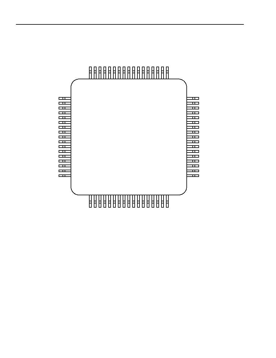
The pinout for the LG1600FXH is shown in Figure 9.
12-3233(F)r.1
Figure 9. Pin Diagram
DNC
DNC
V
REF
C
EXT
R
EXT
LOS
DNC
GND
GND
GND
GND
GND
GND
GND
GND
GND
GND
1
4
7
9
11
14
17
18
26
31
34
V
≠C
LK
O
V
+CL
K
O
NIC
GND
GND
GND
GND
GND
GND
GND
GND
GND
GND
GND
GND
GND
GND
V
≠TH
V
≠FB
V
+OUT
V
≠OUT
V
SS
GND
GND
GND
GND
GND
GND
GND
GND
GND
GND
GND
GND
51
48
43
38
35
68
65
NI
C
V
+F
B
V
+I
N
V
≠IN
GND
GND
GND
GND
GND
GND
GND
GND
GND
GND
GND
GND
GND
60
55
52
2
3
5
6
8
10
12
13
15
16
19 20 21 22 23 24 25
27 28 29 30
32 33
36
37
39
40
41
42
44
45
46
47
49
50
53
54
56
57
58
59
67 66
64 63 62 61
Data Sheet
August 1999
LG1600FXH Clock and Data Regenerator
7
Lucent Technologies Inc.
Pin Information
(continued)
The pin descriptions for the LG1600FXH are given in Table 1.
Table 1. Pin Descriptions
Pin
Symbol
Name/Description
1, 4, 17
DNC
Do Not Connect. Internal test point or reserved for future use.
7
V
REF
Reference Voltage. Nominally ≠3.2 V. Can be used to bias LG1605DXB
(see data sheet). Load
10 k
.
9
C
EXT
Terminal for optional external capacitor to increase PLL damping (normally
not connected).
11
R
EXT
Terminal for external resistor to set PLL bandwidth (Required).
14
LOS
Loss of Signal Indicator. Provides approximately 1 mA sink current with
data signal present, can interface to CMOS, TTL when connected to logic
V
DD
through a 10 k
resistor. Normally grounded when not used.
26
V
≠CLKO
Recovered Clock Out. ac couple or terminate into 50
to GND.
31
V
+CLKO
Recovered Clock Out. ac couple or terminate into 50
to GND.
35
V
SS
Supply Voltage. ≠5.2 Vdc nominal.
Warning: Connecting a positive voltage to this pin will permanently
damage the device.
38
V
≠OUT
Regenerated Data Out. ac couple or terminate into 50
to GND.
43
V
+OUT
Regenerated Data Out. ac couple or terminate into 50
to GND.
48
V
≠FB
dc Feedback Voltage. Connect to V
≠TH
.
51
V
≠TH
Input Threshold Voltage. Connect to V
≠FB
.
55
V
≠IN
Negative Data Input. Internally ac coupled.
60
V
+IN
Positive Data Input. Internally ac coupled.
65
V
+FB
dc Feedback Voltage. Internally connected; not normally used.
18, 68
NIC
No Internal Connection. May be grounded.
2, 3, 5, 6,
8, 10, 12,
13, 15, 16,
19, 20, 21,
22, 23, 24,
25, 27, 28,
29, 30, 32,
33, 34, 36,
37, 39, 40,
41, 42, 44,
45, 46, 47,
49, 50, 52,
53, 54, 56,
57, 58, 59,
61, 62, 63,
64, 66, 67
GND
Ground. Connect to top ground plane of coplanar/microstrip circuit board.
Body
GND
Ground. Does not need to be connected. GND pins provide all necessary
ground connections.
Data Sheet
LG1600FXH Clock and Data Regenerator
August 1999
8
Lucent Technologies Inc.
Absolute Maximum Ratings
Stresses in excess of the absolute maximum ratings can cause permanent or latent damage to the device. These
are absolute stress ratings only. Functional operation of the device is not implied at these or any other conditions in
excess of those given in the operational sections of the data sheet. Exposure to absolute maximum ratings for
extended periods can adversely affect device reliability.
Table 2. Absolute Maximum Ratings
Recommended Operating Conditions
Table 3. Recommended Operating Conditions
Handling Precautions
Although protection circuitry has been designed into this device, proper precautions should be taken to avoid expo-
sure to electrostatic discharge (ESD) during handling and mounting. Lucent Technologies Microelectronics Group
employs a human-body model (HBM) for ESD-susceptibility testing and protection design evaluation. The HBM
(resistance = 1500
, capacitance = 100 pF) is used. The HBM ESD threshold presented in Table 4 was obtained
by using these circuit parameters.
Table 4. ESD Threshold
Mounting and Connections
Certain precautions must be taken when using solder. For installation using a constant temperature solder, temper-
atures of under 300 ∞C may be employed for periods of time up to 5 seconds, maximum. For installation with a sol-
dering iron (battery operated or nonswitching only), the soldering tip temperature should not be greater than
300 ∞C and the soldering time for each lead must not exceed 5 seconds.
Parameter
Min
Max
Unit
Supply Voltage Range (V
SS
)
≠7
0.5
V
Loss of Signal Bias Voltage (V
DD
)
--
7
V
Power Dissipation
--
2
W
Voltage (all pins)
V
SS
0.5
V
Transient Voltage to ac Couple Pins (V
±IN
, R
EXT
)
--
±3
V
Storage Temperature Range
≠40
125
∞C
Operating Temperature Range
≠40
100
∞C
Parameter
Symbol
Min
Max
Unit
Case Temperature
t
CASE
0
70
∞C
Power Supply
V
SS
≠4.7
≠5.7
V
HBM ESD Threshold
Device
Voltage
LG1600FXH
200 V
Data Sheet
August 1999
LG1600FXH Clock and Data Regenerator
9
Lucent Technologies Inc.
Electrical Characteristics
t
CASE
= 0 ∞C to 70 ∞C, V
SS
= ≠4.7 V to ≠5.7 V, V
DD
= 5 V, bit rate = f
B
Gbits/s ±0.05% NRZ and data pattern =
2
23
≠ 1 PRBS, 200 mV
V
±IN
800 mV, BER < 1e
≠9
, unless otherwise indicated.
Note: Minimum and maximum values are testing requirements. Typical values are characteristics of the device and
are the result of engineering evaluations. Typical values are for information purposes only and are not part of
the testing requirements.
Parameter
Symbol
Conditions
Min
Typ
Max
Unit
Data Input Voltage
V
≠IN
Single ended on either input
200
--
800
mVp-p
Data Input Voltage
V
+IN ≠
V
≠IN
Differential
200
--
1600
mVp-p
Data Output Voltage
V
±OUT
ac coupled
625
750
900
mVp-p
Data Output Voltage
V
±OUT
dc coupled
650
800
900
mVp-p
Clock Output Voltage
V
±CLKO
dc coupled
650
750
900
mVp-p
Clock Output Voltage
V
±CLKO
ac coupled; f
B
3 Gbits/s
625
750
900
mVp-p
Clock Output Voltage
V
±CLKO
ac coupled; f
B
> 3 Gbits/s
500
600
900
mVp-p
Output Pulse Width Rela-
tive to Bit Period T = 1/f
B
PW%
t
CASE
= 40 ∞C
90
100
110
%
Clock Output Duty Cycle
DC
CLKO
t
CASE
= 40 ∞C
40
--
60
%
Clock/Data Output Transi-
tion Time
t
r
, t
f
20% to 80%
--
80
100
ps
Maximum Bit Error Rate
BER
MAX
Jitter modulation @ f
B
◊
40 kHz,
t
CASE
= 40 ∞C
1e
≠3
--
--
--
LOS Output Voltage, Low
V
LOSL
R
L
= 10 k
≠1
≠0.8
0.5
V
LOS Output Voltage, High
V
LOSH
R
L
= 10 k
, V
≠IN
= 0 V
V
DD
≠
0.5
V
DD
V
DD
V
Loss of Signal Delay
LOS
Measured from last data transi-
tion, t
CASE
= 40 ∞C
10
30
100
µs
Jitter Generation
J
GEN
--
--
0.005
0.01
UI
Jitter Transfer Bandwidth
J
BW
User adjustable with R
X
as sug-
gested by Figure 8, t
CASE
= 25 ∞C
--
f
B
--
MHz
Output Reference Voltage
V
REF
Load to ground
20 k
≠3.4
≠3.15
≠2.9
V
Jitter Tolerance
J
TOL
f
mod
f
B
x 40 kHz, t
CASE
= 40 ∞C
f
B
x 40 kHz
f
mod
f
B
◊
400 kHz,
t
CASE
= 40 ∞C
f
mod
f
B
◊
400 kHz,
t
CASE
= 40 ∞C
1.5
0.6 f
B
/
f
mod
0.15
5
2 f
B
/f
mod
0.5
--
--
--
UI
UI
UI
Acquisition/Recovery
Time
ACQ
Measured from first data
transition
*
, t
CASE
= 40 ∞C
* Parameter guaranteed by design or characterization and not production tested.
--
600
800
µs
Supply Current
I
SS
≠5.7 V
V
SS
≠4.7 V
--
290
320
mA
Data Sheet
LG1600FXH Clock and Data Regenerator
August 1999
10
Lucent Technologies Inc.
Test Circuit
12-3234(F)r.6
Notes:
Resistor R
X
determines the PLL bandwidth and is required for normal operation. The LG1600FXH differs in this respect from the LG1600AXD
CDR, which has an internal resistor that sets a minimum bandwidth. The recommended value is 140
for optimal jitter transfer performance.
Capacitor C
X
is optional and can be used to increase the damping of the PLL in critical applications.
The outputs may be either ac coupled, as indicated, or dc terminated into 50
. In the first case, good output return loss can be obtained. The
latter configuration provides a 0 mV to ≠800 mV output swing for easy interface to dc-coupled circuits.
Figure 10. LG1600FXH Typical Test Circuit
500 k
+
VCO
Q
D
V
+
CLKO
V
≠
CLKO
31
26
D
FREQ. &
PHASE
DETECT.
0∞
90∞
LOOP CONTROL &
SIGNAL DETECT
11
14
9
7
V
REF
C
EXT
R
EXT
LOS
V
≠TH
51
V
≠FB
48
55
60
65
V
≠IN
V
+IN
V
+FB
0.047
µ
F
0.047
µ
F
0.047
µ
F
0.047
µ
F
1 k
50
25 k
50
25 k
1 k
43
38
V
+OUT
V
≠OUT
35
0.047
µ
F
50
50
DATA
GENERATOR
OPTIONAL
THRESHOLD
CONTROL
ALTERNATIVE
50
50
OPTIONAL
C
a
> 0.1
µ
F/f
B
V
SS
5.2 V
+
OPTIONAL
C
b
> 100 pF/f
B
50
50
C
X
OPTIONAL
(SEE TEXT)
R
X
= 140
REQUIRED
0.047
µ
F
10 k
V
DD
5 V
+
V
LOS
V
SS
Data Sheet
August 1999
LG1600FXH Clock and Data Regenerator
11
Lucent Technologies Inc.
Typical Performance Characteristics
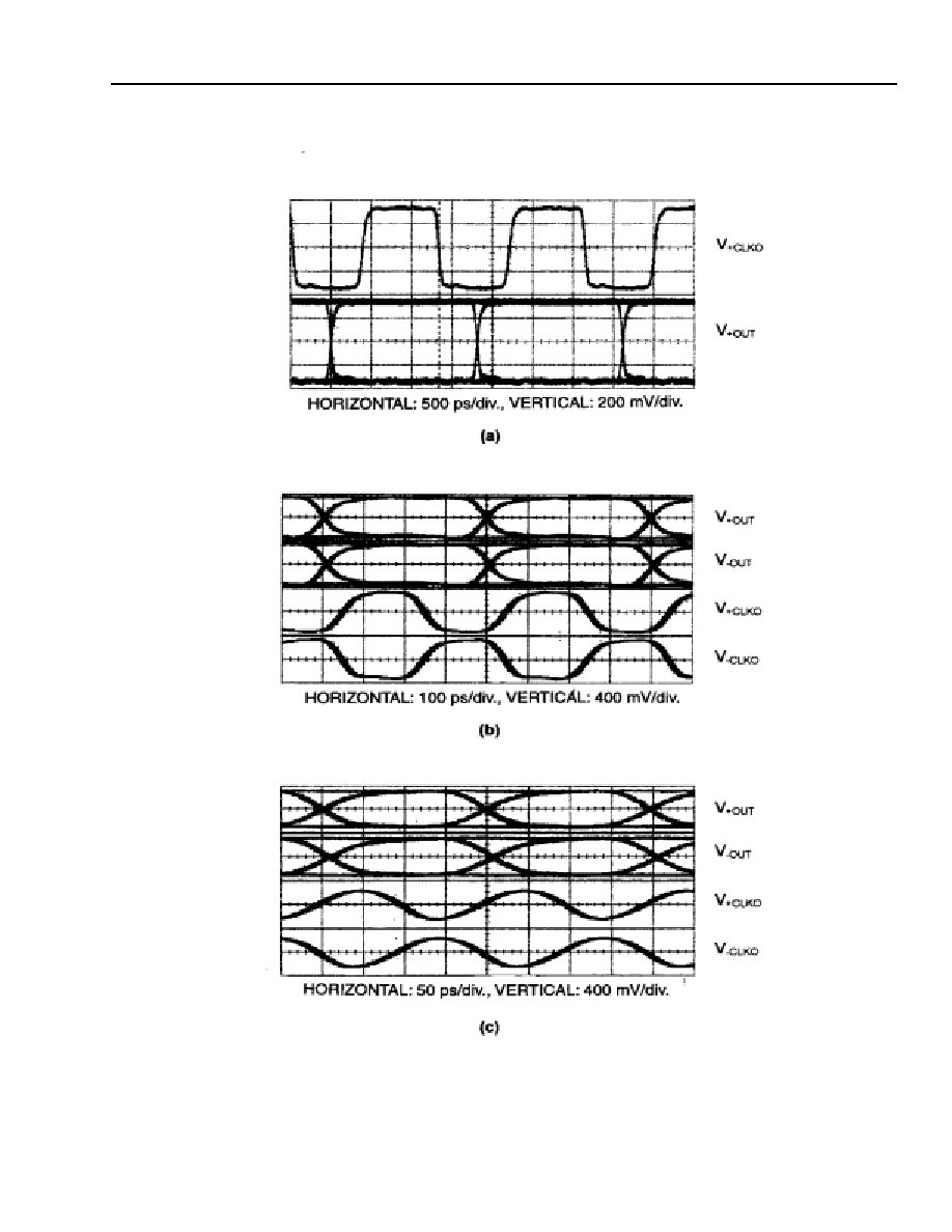
Figure 11. LG1600FXH Typical Eye Patterns
LG1600FXH0553
LG1600FXH2488
LG1600FXH4977
Data Sheet
LG1600FXH Clock and Data Regenerator
August 1999
12
Lucent Technologies Inc.
Typical Performance Characteristics
(continued)
12-3235(F)r.2
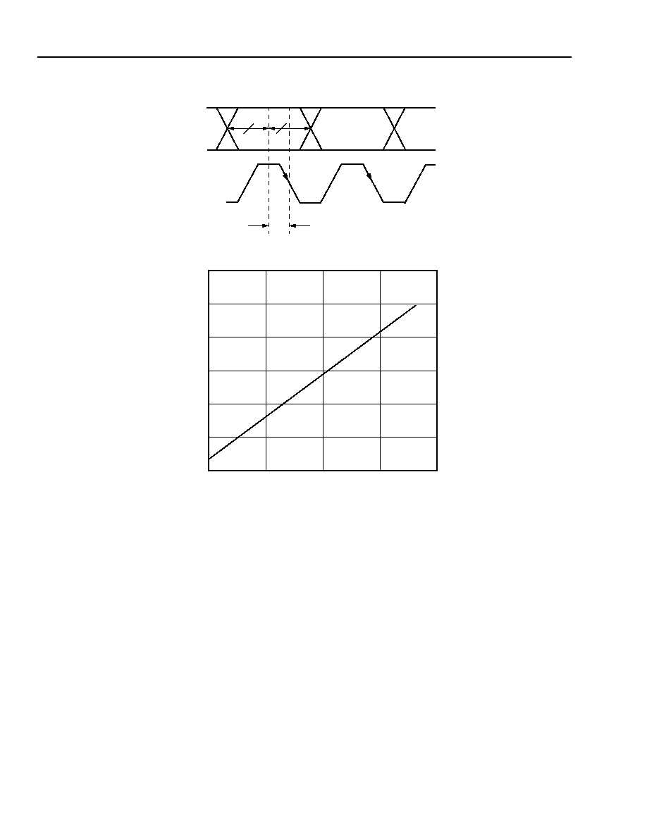
Figure 12. Data Clock Output Timing Diagram
0
500
1500
2000
≠100
100
200
300
500
BIT PERIOD (ps)
0
1000
400
OUTPUT
TI
MI
NG (
p
s
)
OUTPUT TIMING
y = 1/4x ≠ 65
V±
OUT
V+
CLKO
Data Sheet
August 1999
LG1600FXH Clock and Data Regenerator
13
Lucent Technologies Inc.
Typical Performance Characteristics
(continued)
12-3236(F)r.3
Figure 13. Error Recovery Timing Diagram
0
200
400
800
0
100
300
400
500
700
INPUT BLANKING (
µ
s)
200
600
600
RE
CO
V
E
RY
TIME
(
µ
s)
BLANKING
INPUT
OUTPUT
ERROR
ERROR RECOVERY
1000
PULSE
DATA
DATA
SIGNAL
TIME
Data Sheet
LG1600FXH Clock and Data Regenerator
August 1999
14
Lucent Technologies Inc.
Typical Performance Characteristics
(continued)
12-3237(F)r.4
Figure 14. Error Recovery Test Circuit
ERROR DETECTOR
TRIG
OUT
PULSE
GENERATOR
CH3
CH2
CH1
LF
OSCILLOSCOPE
CLK
DATA
DATA
CLK
BLNK
PATTERN
GENERATOR
DATA
IN
DATA
OUT
CLK OUT
CH1
CH2
CH3
DIGITIZING
OSCILLOSCOPE
MIXER
Data Sheet
August 1999
LG1600FXH Clock and Data Regenerator
15
Lucent Technologies Inc.
Outline Diagram
68-Pin Surface-Mount Package
Dimensions are in inches.
12-3350(F).ar.1
0.015 TYP
0.050 TYP
1.370 ± 0.10
0.010
DETAIL A
0.158
0.010
≠0.002
0.030
0--5
∞
R0.020
DETAIL A
+0.005
1
17
18
34
35
51
52
68
1.180
0.590

Data Sheet
LG1600FXH Clock and Data Regenerator
August 1999
16
Lucent Technologies Inc.
Ordering Information
Device Code
Package
Temperature
Comcode
LG1600FXHXXXX
Surface-Mount Package
0 ∞C to 70 ∞C
107236143
LG1600FXH0500
Surface-Mount Package
0 ∞C to 70 ∞C
107914038
LG1600FXH0553
Surface-Mount Package
0 ∞C to 70 ∞C
107236101
LG1600FXH0622
Surface-Mount Package
0 ∞C to 70 ∞C
107339244
LG1600FXH1200
Surface-Mount Package
0 ∞C to 70 ∞C
107841447
LG1600FXH1244
Surface-Mount Package
0 ∞C to 70 ∞C
107386179
LG1600FXH1298
Surface-Mount Package
0 ∞C to 70 ∞C
107236127
LG1600FXH1555
Surface-Mount Package
0 ∞C to 70 ∞C
107914046
LG1600FXH2380
Surface-Mount Package
0 ∞C to 70 ∞C
107236135
LG1600FXH2433
Surface-Mount Package
0 ∞C to 70 ∞C
107645939
LG1600FXH2488
Surface-Mount Package
0 ∞C to 70 ∞C
107081879
LG1600FXH2666
Surface-Mount Package
0 ∞C to 70 ∞C
107386187
LG1600FXH2949
Surface-Mount Package
0 ∞C to 70 ∞C
107385650
LG1600FXH3111
Surface-Mount Package
0 ∞C to 70 ∞C
107394132
LG1600FXH3840
Surface-Mount Package
0 ∞C to 70 ∞C
107840423
LG1600FXH4977
Surface-Mount Package
0 ∞C to 70 ∞C
107081887
LG1600FXH5332
Surface-Mount Package
0 ∞C to 70 ∞C
107081895
TF1004A
Test Fixture
--
106497621
Data Sheet
August 1999
LG1600FXH Clock and Data Regenerator
17
Lucent Technologies Inc.
Appendix
The test fixture mentioned in the data sheet is sold separately and is described in detail below.
5-7831(F)
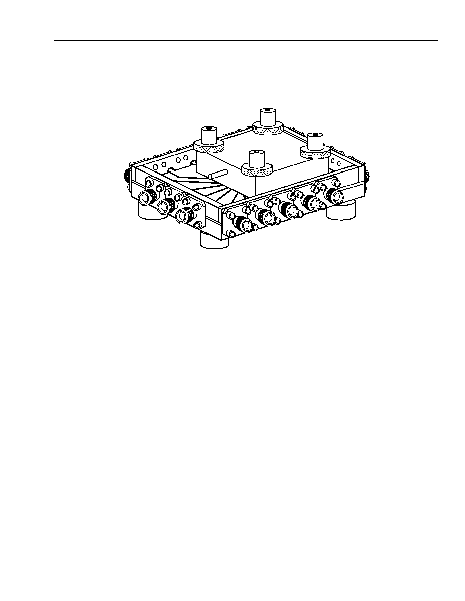
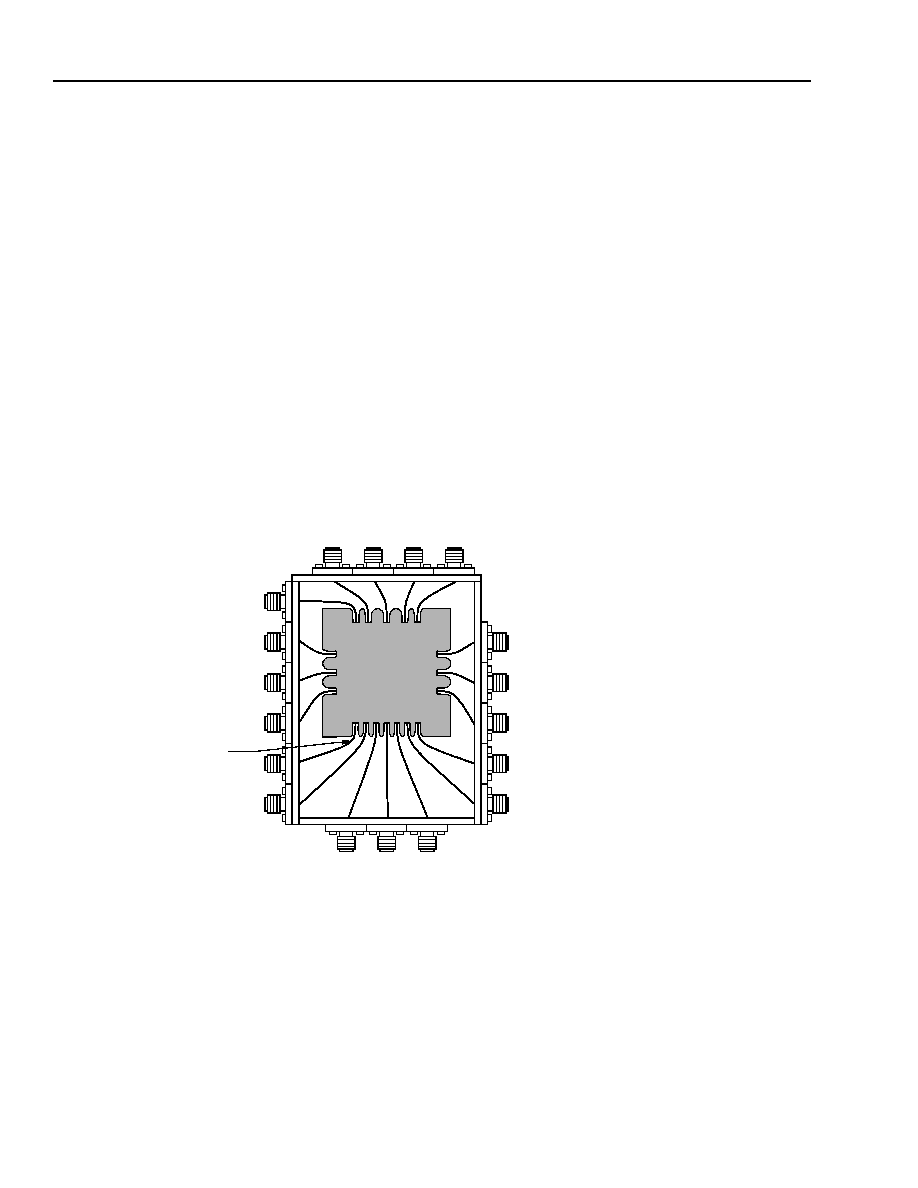
Figure 15. TF1004A Test Fixture
TF1004A Test Fixture Features
s
SMA connectors
s
Easy package placement
s
Good RF performance
Test Fixture Functional Description
The TF1004A test fixture is used to characterize 68-pin surface-mount packages for high-speed fiber-optic commu-
nications. The fixture consists of a metallized substrate (PTFE filled material) fastened to a brass base with RF
connectors and mounting hardware for the package. The package leads make contact to the circuit traces on the
fixture through use of a pressure ring and four finger nuts.
The TF1004A is preassembled and fully tested prior to shipment.
Before Use of Test Fixture
s
Due to possible stress during shipment, SMA connectors may be misaligned.
s
Check each SMA for continuity.
s
If necessary, realign and retighten with a 5/64 in. hex key wrench.
Data Sheet
LG1600FXH Clock and Data Regenerator
August 1999
18
Lucent Technologies Inc.
Appendix
(continued)
Instructions for Use of Test Fixture
A pair of flat-tip tweezers can be used to insert or remove a package from the test fixture. Always wear a grounding
strap to prevent ESD.
1. To insert a package, remove the four finger nuts and gently lift the pressure ring off of the test fixture.
2. Place the pressure ring, cavity side up, on a flat ESD safe surface.
3. Connect the metal tube to any general-purpose vacuum source with flexible tubing. The vacuum source should
be off.
4. Place the package, lid down, on a flat ESD safe surface. Locate pin 1 on the package.
5. Insert the package into the pressure ring (lid down) with pin 1 located next to the orientation mark and turn on
the vacuum. The vacuum will retain the package in the pressure ring during the following steps.
6. Align the vertically conductive material on the circuit board.
7. Place the pressure ring down over the alignment pins and gently tighten the finger nuts.
8. Remove vacuum, if desired. The vacuum source tubing can be removed for convenience.
5-7832(F)r.1
Figure 16. TF1004A Connector Assignment
V
+CLK
V
≠CLK
NIC
DNC
LOS
V
≠FB
V
+OUT
V
≠OUT
V
SS
V
≠TH
DNC
DNC
V
≠IN
V
+IN
V
+FB
(48)
(43)
(38)
(35)
(51)
(55)
(60)
(1)
(4)
(7)
(11)
(9)
(14)
(17)
(18)
(26)
(31)
V
REF
C
EXT
R
EXT
(65)
PIN #1
NIC = NO INTERNAL CONNECTION
DNC = DO NOT CONNECT
(##) = PACKAGE PIN NUMBER

Data Sheet
August 1999
LG1600FXH Clock and Data Regenerator
19
Lucent Technologies Inc.
Notes

LG1600FXH Clock and Data Regenerator
Preliminary Data Sheet
Interactive Terminal Transmission Convergence
August 1999
For additional information, contact your Microelectronics Group Account Manager or the following:
INTERNET:
http://www.lucent.com/micro
E-MAIL:
docmaster@micro.lucent.com
N. AMERICA:
Microelectronics Group, Lucent Technologies Inc., 555 Union Boulevard, Room 30L-15P-BA, Allentown, PA 18103
1-800-372-2447, FAX 610-712-4106 (In CANADA: 1-800-553-2448, FAX 610-712-4106)
ASIA PACIFIC: Microelectronics Group, Lucent Technologies Singapore Pte. Ltd., 77 Science Park Drive, #03-18 Cintech III, Singapore 118256
Tel. (65) 778 8833, FAX (65) 777 7495
CHINA:
Microelectronics Group, Lucent Technologies (China) Co., Ltd., A-F2, 23/F, Zao Fong Universe Building, 1800 Zhong Shan Xi Road, Shanghai
200233 P. R. China Tel. (86) 21 6440 0468, ext. 316, FAX (86) 21 6440 0652
JAPAN:
Microelectronics Group, Lucent Technologies Japan Ltd., 7-18, Higashi-Gotanda 2-chome, Shinagawa-ku, Tokyo 141, Japan
Tel. (81) 3 5421 1600, FAX (81) 3 5421 1700
EUROPE:
Data Requests: MICROELECTRONICS GROUP DATALINE: Tel. (44) 7000 582 368, FAX (44) 1189 328 148
Technical Inquiries: GERMANY: (49) 89 95086 0 (Munich), UNITED KINGDOM: (44) 1344 865 900 (Ascot),
FRANCE: (33) 1 40 83 68 00 (Paris), SWEDEN: (46) 8 594 607 00 (Stockholm), FINLAND: (358) 9 4354 2800 (Helsinki),
ITALY: (39) 02 6608131 (Milan), SPAIN: (34) 1 807 1441 (Madrid)
Lucent Technologies Inc. reserves the right to make changes to the product(s) or information contained herein without notice. No liability is assumed as a result of their use or application. No
rights under any patent accompany the sale of any such product(s) or information.
Copyright © 1999 Lucent Technologies Inc.
All Rights Reserved
Printed in U.S.A.
August 1999
DS99-186HSPL (Replaces DS96-237FCE)