 | –≠–ª–µ–∫—Ç—Ä–æ–Ω–Ω—ã–π –∫–æ–º–ø–æ–Ω–µ–Ω—Ç: LG1605DXB | –°–∫–∞—á–∞—Ç—å:  PDF PDF  ZIP ZIP |
Data Sheet
February 1999
LG1605DXB Limiting Amplifier
Features
s
28 dB gain, 34 dB differential
s
Large dynamic range: >60 dB
s
Wideband response: 8 kHz to 3 GHz
s
Extremely low ±4 ps delay skew across input range
s
Complementary 50
I/Os
s
Surface-mount package
s
Standard ECL supply (400 mW)
Applications
s
Data/clock main amplifier SONET/SDH OC-48/
STM-16 transmission systems, DWDM systems
s
Digital video transmission
s
Interface between 1319 receiver and LG1600
clock and data regenerator
s
High-speed comparator
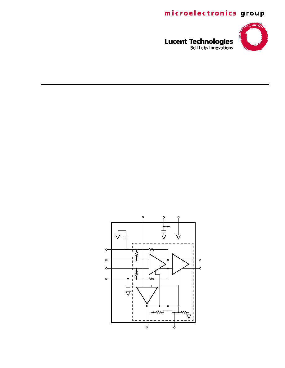
Functional Description
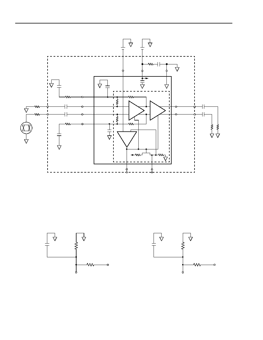
The LG1605DXB is a GaAs wideband limiting ampli-
fier with differential inputs and outputs that provides
28 dB of gain (34 dB differential) and 3 GHz of band-
width in a 50
environment (Figure 1 shows the
block diagram). At low input levels, below 10 mV to
20 mV, the circuit behaves as a linear amplifier. At
higher levels, the device goes smoothly into limiting.
The device matches the performance of an AGC
amplifier but shows none of the AGC bouncing and
attack characteristics.
12-3214(F).r3
Figure 1. LG1605DXB Block Diagram
110 pF
25 k
110 pF
≠
+
13
14
2
3
V
≠OUT
CHIP BOUNDARY
GND
1, 4, 5, 6, 15, 16
7
V
BR
8
+
≠
≠
+
9
10
11
12
110 pF
50
V
SS
V
+OUT
V
BS
V
BF
V
+REF
V
+IN
V
≠IN
V
≠REF
25 k
+
≠
≠
+
50
Data Sheet
LG1605DXB Limiting Amplifier
February 1999
2
Lucent Technologies Inc.
Functional Description
(continued)
The amplifier has a virtually constant output delay for
input signal levels, varying across three decades. As a
result, the device has very low amplitude-to-phase con-
version, which makes it ultimately suitable for applica-
tions in highly sensitive fiber-optic systems. Although
the amplifier is most sensitive when the input is ac cou-
pled (see Figure 3), a low offset (<25 mV) and a large
common-mode input range of 2 V make it useful in
applications that require a high-speed comparator as
well.
A unique input coupling arrangement allows for a fre-
quency response down into the low kHz range while
using coupling capacitors that are small enough to
maintain a good input return loss at high frequencies.
The outputs, when ac coupled, provide a good RF ter-
mination up to very high frequencies. The associated
ability to absorb reflections returning from the receiving
end is essential for preventing intersymbol interference
in fiber-optic systems.
The amplifier is a natural step-up interface between
receivers, such as the Lucent Technologies Micro-
eletronics Group Optoelectronics unit 1319 and regen-
erators like the Lucent Technologies Microelectronics
Group LG1600. The referred wideband input noise
(168 µVrms typical) allows for a <1e≠9 bit error rate
(BER) for inputs down to 2 mVp-p (S/N ratio of
21.5 dB).
In SAW based clock recovery systems, with clock fre-
quencies as high as 2.5 GHz, the device can provide a
clock-limiting function in systems.
The LG1605DXB is available in a hermetically sealed,
16-lead, glass-metal surface-mount package and uses
a standard ECL supply.
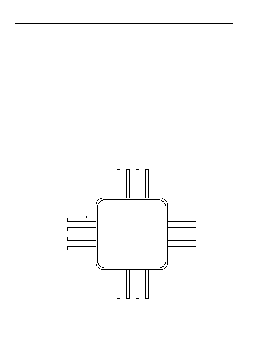
Pin Information
The pinout for the LG1605DXB is shown in Figure 2.
12-3223(F)
Figure 2. Pin Diagram
GND
GND
1
2
3
4
V
+REF
12
11
10
9
16
15
14
13
GND GND V
BS
5
6
7
8
GND GND
V
BF
V
+IN
V
≠IN
V
≠REF
V
SS
V
BR
V
+OUT
V
≠OUT
Data Sheet
February 1999
LG1605DXB Limiting Amplifier
3
Lucent Technologies Inc.
Pin Information
(continued)
The pin descriptions for the LG1605DXB are given in Table 1.
Table 1. Pin Descriptions
Pin
Symbol
Name/Description
2
V
+OUT
Positive Data Output.
3
V
≠OUT
Negative Data Output.
7
V
SS
dc Supply Voltage.
8
V
BR
Bias Reference Voltage. Connect to nominal ≠1.5 V stable voltage refer-
ence, bypassed to GND with a capacitor
0.047 µF.
9
V
≠REF
Data Negative Reference. Internally bypassed with 110 pF. Broadband
operation requires up-close external bypassing with a capacitor
0.047 µF,
matching the input coupling capacitor.
10
V
≠IN
Negative Data Input. Requires ac-coupling capacitor and 50
source or
termination.
11
V
+IN
Positive Data Input.
12
V
+REF
Data Positive Reference. See pin 9 above.
13
V
BF
Bias Force Voltage. Obsolete function, do not connect.
14
V
BS
Bias Sense Voltage. Internal test point, tracking V
BR
. Normally not con-
nected.
1, 4, 5, 6,
15, 16,
Package
Back
GND
Ground. For optimum performance, package back should contact board
ground plane. (See the Mounting and Connections section.)

Data Sheet
LG1605DXB Limiting Amplifier
February 1999
4
Lucent Technologies Inc.
Absolute Maximum Ratings
Stresses in excess of the absolute maximum ratings can cause permanent or latent damage to the device. These
are absolute stress ratings only. Functional operation of the device is not implied at these or any other conditions in
excess of those given in the operational sections of the data sheet. Exposure to absolute maximum ratings for
extended periods can adversely affect device reliability.
Table 2. Absolute Maximum Ratings
Recommended Operating Conditions
Table 3. Recommended Operating Conditions
Handling Precautions
Although protection circuitry has been designed into this device, proper precautions should be taken to avoid expo-
sure to electrostatic discharge (ESD) during handling and mounting. Lucent employs a human-body model (HBM)
and a charged-device model (CDM) for ESD-susceptibility testing and protection design evaluation. No industry-
wide standard has been adopted for the CDM. However, a standard HBM (resistance = 1500
, capacitance =
100 pF) is widely used and, therefore, can be used for comparison purposes. The HBM ESD threshold presented
here was obtained by using these circuit parameters.
Table 4. ESD Threshold
Mounting and Connections
Certain precautions must be taken when using solder. For installation using a constant temperature solder, temper-
atures of under 300 ∞C may be employed for periods of time up to 5 s, maximum. For installation with a soldering
iron (battery operated or nonswitching only), the soldering tip temperature should not be greater than 300 ∞C and
the soldering time for each lead must not exceed 5 s. This device is supplied with solder on the back of the pack-
age. Due to the high gain of the device, it is recommended to solder the back of the package to ground.
Parameter
Min
Max
Unit
Supply Voltage Range (V
SS
)
≠7
0.5
V
Power Dissipation
--
1
W
Voltage (all pins)
V
SS
0.5
V
V
+REF
≠ V
+IN
--
±2
V
V
≠REF
≠ V
≠IN
--
±2
V
Storage Temperature Range
≠40
125
∞C
Operating Case Temperature Range
0
100
∞C
Parameter
Symbol
Min
Max
Unit
Case Temperature
t
CASE
0
70
∞C
Power Supply
V
SS
≠5.7
≠4.7
V
HBM ESD Threshold
Device
Voltage
LG1605DXB
200 V
Data Sheet
February 1999
LG1605DXB Limiting Amplifier
5
Lucent Technologies Inc.
Mounting and Connections
(continued)
Lucent Technologies/FORCE ICs assembly procedure recommendations for the LG1605DXB are as follows:
s
Board solder pattern for the 1605DXB package base should not exceed 50% of the package base area.
s
Back lighting can be used during the pick and place operation to silhouette the package in order to eliminate
reflection problems with the solder on the bottom.
s
Set the lead spacing tolerance to ±0.012 in.
s
Insertion pressure should not exceed 125 g.
Electrical Characteristics
t
CASE
= 0 ∞C to 70 ∞C, V
BR
= ≠1.5 V, V
SS
= ≠4.7 V to ≠5.7 V, bit rate = 2.488 Mbits/s NRZ, and data pattern =
2
23
≠ 1 PRBS, unless otherwise indicated.
Note: Minimum and maximum values are testing requirements. Typical values are characteristics of the device and
are the result of engineering evaluations. Typical values are for information purposes only and are not part of
the testing requirements.
1. All temperatures are case temperature, t
CASE
.
2. Parameter guaranteed by design or characterization and not production tested.
Parameter
Symbol
Conditions
1
Min
Typ
Max
Unit
Data Input Voltage
2
V
±IN
Single-ended source
--
--
800
mVp-p
Data Input Voltage
2
V
+IN
≠ V
≠IN
Differential source
--
--
1600
mVp-p
Input Offset Voltage
V
+REF
≠ V
≠REF
40 ∞C/≠5.2 V; 70 ∞C/≠5.7 V
--
--
25
mV
Common-mode Input
Voltage Range
V
CMIN
25 ∞C, V
SS
= ≠5.2 V,
dc input coupling
--
≠2 to ≠4
--
V
Output Voltage
V
±OUT
--
400
550
--
mVp-p
Output Pulse Width
Relative to Bit Period
PW%
Measured on V
+OUT
,
@ 40 ∞C and 70 ∞C
90
100
110
%
Small-signal Output
Transition Time
tr, tf
25 ∞C, 20% to 80%,
V
IN
= 8 mVp-p
--
100
--
ps
Small-signal Gain
G
40 ∞C to 70 ∞C, V
IN
=
8 mVp-p
26
28
35
dB
Small-signal ≠3 dB
Bandwidth
f
3dB
25 ∞C, V
IN
= 8 mVp-p
--
3
--
GHz
Low-frequency ≠3 dB
Cut-off
2
f
LF
V
IN
= 8 mVp-p, input coupling
and bypassing as in Figure 3
--
2.5
8
kHz
Supply Current
I
SS
--
--
85
100
mA
Noise Figure
2
NF
25 ∞C, single-ended input
--
15
16
dB
Input Referred Wideband
Noise
V
nr
25 ∞C, single-ended input,
7 kHz--18 GHz
--
168
--
µVrms
Thermal Resistance
JC
Junction to case
--
30
--
∞C/W
Data Sheet
LG1605DXB Limiting Amplifier
February 1999
6
Lucent Technologies Inc.
Test Circuit
12-3215(F)r.6
1. Depending on the desired supply rejection, V
BR
can be biased with a simple resistive divider, or resistor/zener diode network.
Alternatively, when the LG1605DXB is followed by the LG1600 clock and data regenerator, a resistive divider with bypassing capacitor may
be connected to pin 7 (V
REF
) of the LG1600 (V
REF
≠3.2 V). This arrangement provides excellent temperature stability and power supply
rejection.
2. The outputs may be either ac coupled, as indicated, or dc terminated into 50
. In the first case, good output return loss (see Figure 8) can be
obtained. The latter configuration provides a 0 mV to ≠600 mV output swing (when limiting) for easy interface to dc-coupled circuits. No input
coupling capacitors are needed when interfacing with the LG1600 or the 1319 receiver.
Figure 3. LG1605DXB Test Circuit (with TF1003C Test Fixture)
12-3216(F)r.3
1. Depending on the desired supply rejection, V
BR
can be biased with a simple resistive divider, or resistor/zener diode network.
Alternatively, when the LG1605DXB is followed by the LG1600 clock and data regenerator, a resistive divider with bypassing capacitor may
be connected to pin 7 (V
REF
) of the LG1600 (V
REF
≠3.2 V). This arrangement provides excellent temperature stability and power supply
rejection.
Figure 4. Bias Options
110 pF
25 k
110 pF
≠
+
13
14
2
3
V
≠OUT
CHIP BOUNDARY
GND
1, 4, 5, 6, 15, 16
7
V
BR
8
+
≠
≠
+
9
10
11
12
110 pF
50
V
SS
V
+OUT
V
BS
V
BF
V
+REF
V
+IN
V
≠IN
V
≠REF
25 k
+
≠
≠
+
50
50
50
5
5
LG1605DXB
SOURCE
0.047
µ
F
0.047
µ
F
50
50
LOAD
(SEE NOTE 2)
TF1003C FIXTURE BOUNDARY
0.047
µ
F
+
1.5 V
R
INT
10 k
(SEE NOTE 1)
+
5.2 V
5
0.047
µ
F
0.047
µ
F
0.047
µ
F
0.047
µ
F
0.047
µ
F
(SEE NOTE 1)
12 k
≠3.2 V
(PIN 7 LG1600)
13.6 k
≠1.5 V
A. Using LG1600 Reference Voltage
B. Using Supply Voltage
V
REF
V
BR
0.047
µ
F
(SEE NOTE 1)
8.2 k
≠5.2 V
20 k
≠1.5 V
V
SS
V
BR
Data Sheet
February 1999
LG1605DXB Limiting Amplifier
7
Lucent Technologies Inc.
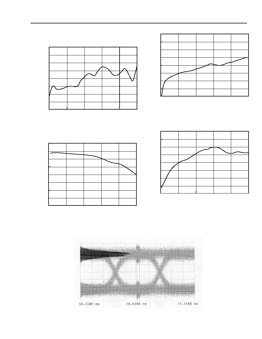
Typical Performance Characteristics
(at T
A
= 25 ∞C)
12-3217(F)
Figure 5. Input Return Loss S
11
12-3218(F)
Figure 6. Gain S
21
0
1
2
3
5
FREQUENCY (GHz)
I
N
P
U
T
RE
TU
RN
L
O
S
S
S
11
(d
B
)
4
≠40
≠20
≠15
≠10
≠5
0
≠25
≠30
≠35
0
1
2
3
5
FREQUENCY (GHz)
GA
I
N
S
21
(d
B
)
4
0
20
25
30
35
40
15
10
5
12-3219(F)
Figure 7. Isolation S
12
12-3220(F)
Figure 8. Output Return Loss S
22
0
1
2
3
5
FREQUENCY (GHz)
IS
O
L
A
T
I
O
N
S
12
(d
B
)
4
≠80
≠40
≠30
≠20
≠10
0
≠50
≠60
≠70
0
1
2
3
5
FREQUENCY (GHz)
OU
TP
UT RE
TUR
N
LO
S
S
S
22
(d
B
)
4
≠40
≠20
≠15
≠10
≠5
0
≠25
≠30
≠35
HORIZONTAL: 100 ps/div, VERTICAL: 12 mV/div; V
IN
= 2.23 mVp-p, V
OUT
= 58.8 mVp-p,
= 4.45 mVrms
Figure 9. Output Noise Histogram
Data Sheet
LG1605DXB Limiting Amplifier
February 1999
8
Lucent Technologies Inc.
Typical Performance Characteristics
(at T
A
= 25 ∞C) (continued)
6 mVp-p
12 mVp-p
50 mVp-p
400 mVp-p
800 mVp-p
HORIZONTAL: 100 ps/div
A. Input Voltage
VERTICAL: 200 mV/div
VERTICAL: 200 mV/div
VERTICAL: 200 mV/div
VERTICAL: 200 mV/div
VERTICAL: 200 mV/div
HORIZONTAL: 100 ps/div
B. Output Voltage
1
10
100
1000
10
1000
INPUT VOLTAGE (mVp-p)
100
O
U
T
P
U
T
V
O
LT
AGE
(
m
Vp-
p
)
1
10
100
1000
INPUT VOLTAGE (mVp-p)
≠10
10
8
6
4
2
0
≠2
≠4
≠6
≠8
RE
LA
T
I
V
E
DE
LA
Y
(ps
)
12-3221(F)
C. Output vs. Input
12-3222(F)
D. Input-to-Output Relative Delay
Figure 10. Limiting Characteristics
Data Sheet
February 1999
LG1605DXB Limiting Amplifier
9
Lucent Technologies Inc.
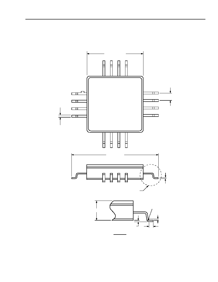
Outline Diagram
16-Pin, Glass-Metal, Surface-Mount Package
Dimensions are in inches.
12-3224(F).b
0.012 TYP
0.030 TYP
0.230 SQ REF
+
0.366
±
0.007
0.005
DETAIL A
0.050 MAX
0.000--0.004
0.020
0--4
∞
DETAIL A
+
9
13
1
5
R0.013
Data Sheet
LG1605DXB Limiting Amplifier
February 1999
10
Lucent Technologies Inc.
Ordering Information
Device Code
Package
Temperature
Comcode
(Ordering Number)
LG1605DXB-TR16
Package on 16 mm tape and reel
0 ∞C to 70 ∞C
107142614
LG1605DXB-FLP
Package in flat pack container
0 ∞C to 70 ∞C
107412025
TF1003C
Test fixture
--
106990138
Data Sheet
February 1999
LG1605DXB Limiting Amplifier
11
Lucent Technologies Inc.
Appendix
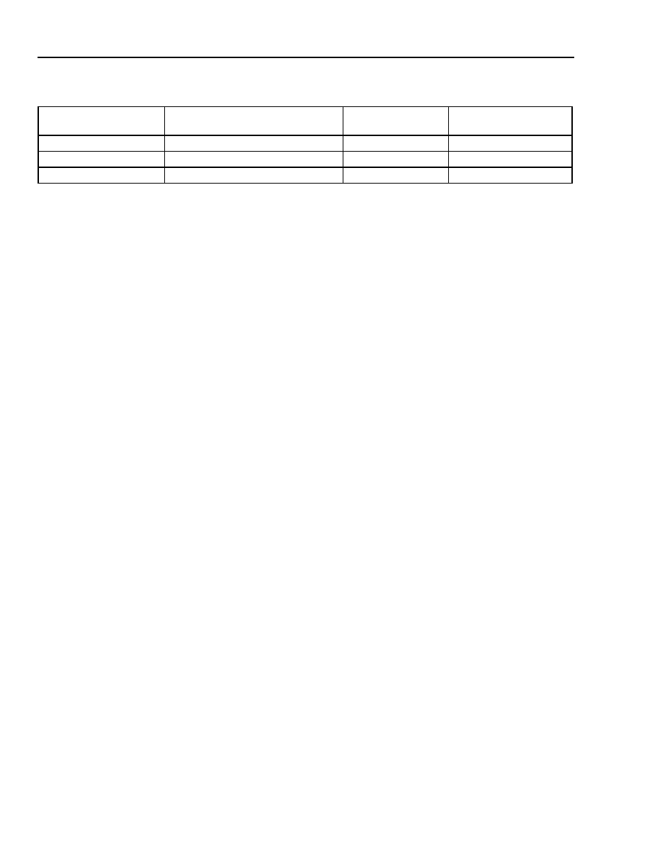
The test fixture mentioned in the data sheet is sold separately and is described in detail below.
5-7208(F).r1
Note: Dot on test fixture lid indicates position of pin 1.
Figure 11. TF1003C Test Fixture
5-7209(F)
Figure 12. TF1003C Electrical Diagram
1
2
3
4
12
11
10
9
13
14
15
16
8
7
6
5
V
+IN
V
≠IN
FIXTURE BOUNDARY
PACKAGE OUTLINE
V
BR
V
SS
V
BF
V
BS
V
+OUT
V
≠OUT
5
0.047
µ
F
0.047
µ
F
0.047
µ
F
0.047
µ
F
5
5
0.047
µ
F
Data Sheet
LG1605DXB Limiting Amplifier
February 1999
Lucent Technologies Inc. reserves the right to make changes to the product(s) or information contained herein without notice. No liability is assumed as a result of their use or application. No
rights under any patent accompany the sale of any such product(s) or information.
FASTCAT is a trademark of Lucent Technologies Inc.
Copyright © 1999 Lucent Technologies Inc.
All Rights Reserved
February 1999
DS98-400HSPL (Replaces DS96-236FCE)
For additional information, contact your Microelectronics Group Account Manager or the following:
INTERNET:
http://www.lucent.com/micro
E-MAIL:
docmaster@micro.lucent.com
N. AMERICA:
Microelectronics Group, Lucent Technologies Inc., 555 Union Boulevard, Room 30L-15P-BA, Allentown, PA 18103
1-800-372-2447, FAX 610-712-4106 (In CANADA: 1-800-553-2448, FAX 610-712-4106)
ASIA PACIFIC: Microelectronics Group, Lucent Technologies Singapore Pte. Ltd., 77 Science Park Drive, #03-18 Cintech III, Singapore 118256
Tel. (65) 778 8833, FAX (65) 777 7495
CHINA:
Microelectronics Group, Lucent Technologies (China) Co., Ltd., A-F2, 23/F, Zao Fong Universe Building, 1800 Zhong Shan Xi Road, Shanghai
200233 P. R. China Tel. (86) 21 6440 0468, ext. 316, FAX (86) 21 6440 0652
JAPAN:
Microelectronics Group, Lucent Technologies Japan Ltd., 7-18, Higashi-Gotanda 2-chome, Shinagawa-ku, Tokyo 141, Japan
Tel. (81) 3 5421 1600, FAX (81) 3 5421 1700
EUROPE:
Data Requests: MICROELECTRONICS GROUP DATALINE: Tel. (44) 1189 324 299, FAX (44) 1189 328 148
Technical Inquiries:GERMANY: (49) 89 95086 0 (Munich), UNITED KINGDOM: (44) 1344 865 900 (Ascot),
FRANCE: (33) 1 40 83 68 00 (Paris), SWEDEN: (46) 8 594 607 00 (Stockholm), FINLAND: (358) 9 4354 2800 (Helsinki),
ITALY: (39) 02 6608131 (Milan), SPAIN: (34) 1 807 1441 (Madrid)
Appendix
(continued)
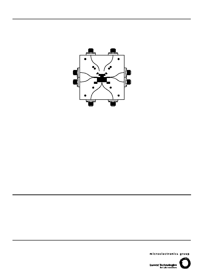
5-7210(F)
Figure 13. TF1003C Connector Assignment (Pressure ring not shown.)
(11)
V
+IN
(10)
V
≠IN
(2)
V
+OUT
(3)
V
≠OUT
(13) V
BF
(14) V
BS
V
BR
(8)
V
SS
(7)