 | –≠–ª–µ–∫—Ç—Ä–æ–Ω–Ω—ã–π –∫–æ–º–ø–æ–Ω–µ–Ω—Ç: LG1628AXA | –°–∫–∞—á–∞—Ç—å:  PDF PDF  ZIP ZIP |

Preliminary Data Sheet
January 1998
LG1628AXA SONET/SDH 2.488 Gbits/s
Transimpedance Amplifier
Features
s
High data rate: 2.5 Gbits/s
s
High gain: 5.8 k
transimpedance
s
Complementary 50
outputs
s
Low noise
s
Ultrawide dynamic range
s
Single ≠5.2 V ECL power supply
Applications
s
SONET/SDH receivers
s
SONET/SDH test equipment
s
Digital video transmission
Functional Description
The Lucent Technologies Microelectronics Group
LG1628AXA is a hybrid integrated circuit that com-
bines the Lucent LG1628A gallium arsenide (GaAs)
transimpedance amplifier chip with an external Si
dual operational amplifier and necessary filtering to
achieve an ultrawide dynamic range amplifier. The
LG1628AXA is capable of handling input currents
from 3
µ
A
avg
to 4 mA
avg
(patent pending). Amplifier
operation is from a single ≠5.2 V power supply. The
targeted transmission system is SONET OC-48 and
SDH STM-16.
A complete receiver/regenerator can be constructed
with an LG1628AXA followed by an LG1605 limiting
amplifier and LG1600 clock and data regenerator.
Figure 1 shows the block diagram of the LG1628AXA
transimpedance amplifier. The amplifier consists of a
4.2 k
differential transimpedance stage followed by
a limiting buffer that provides complementary 50
outputs.
5-5329(F)
Figure 1. LG1628AXA Functional Diagram
GND
V
SS
Z
EFF
50
LIMITING
BUFFER
OUT+
R
F
OUT≠
R
F
OVERLOAD CONTROL
IN≠
IN+
LG1628AXA SONET/SDH 2.488 Gbits/s
Preliminary Data Sheet
Transimpedance Amplifier
January 1998
2
Lucent Technologies Inc.
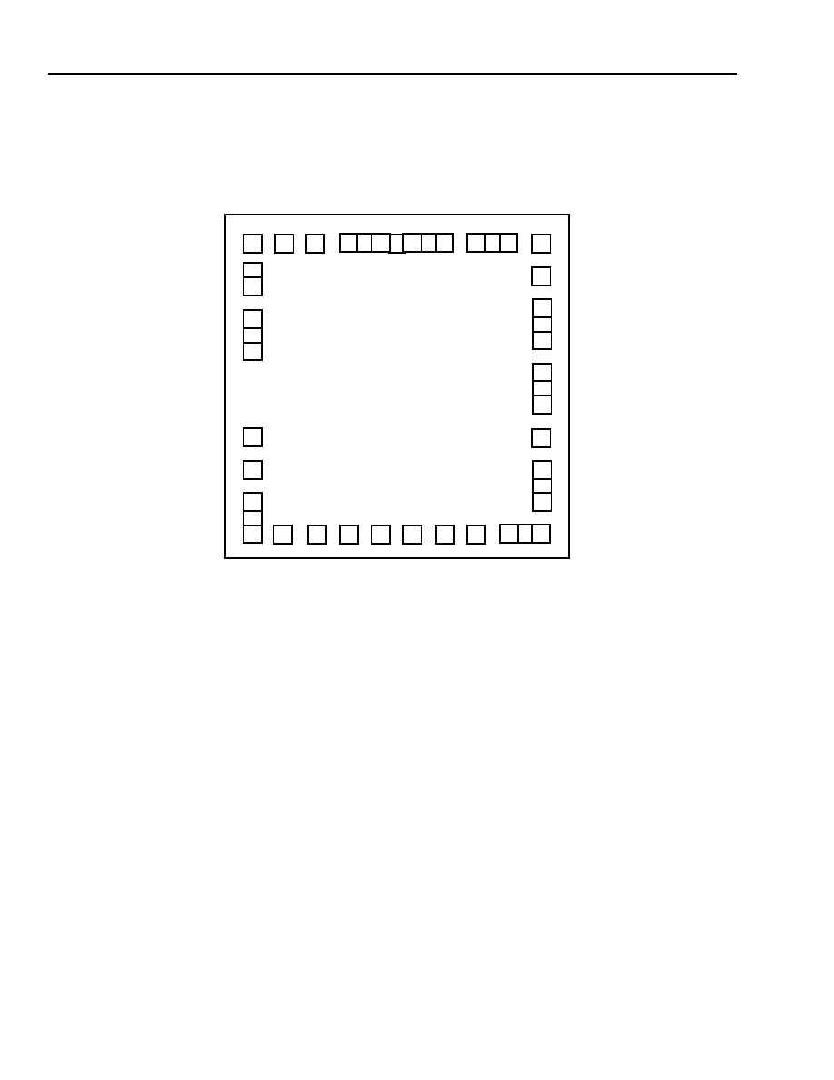
Die Pad Configuration
The die pad configuration is shown in Figure 2.
5-5336(F)r.2
Figure 2. Die Pad Configuration
V
SS2
GND
2
OUT≠
OUT+
GND
2
BG
V
SS1
OP2+B
OP2+A
OP2≠
OP1+
OP1≠
OP1
OUT
OP2
OUT
BYPASS
IN+
GND
1
GND
1
IN≠
GND
1
GND
2
DNC
DNC
DNC
1
2
3
4
5
6
7
8
9
10
11
11
12
12
13
14
14
15
15
16
17
18
18
19
19
19
19
20
21
22
23
24
24
3
OUTSIDE DIE DIMENSIONS:
1.62 mm
2
x 1.62 mm
2
PAD SIZE:
100
µ
m
2
x 100
µ
m
2
(EXCEPT PAD #23, 100
µ
m
2
x 150
µ
m
2
)
PAD SEPARATION:
50
µ
m

Preliminary Data Sheet
LG1628AXA SONET/SDH 2.488 Gbits/s
January 1998
Transimpedance Amplifier
3
Lucent Technologies Inc.
Die Pad Configuration
(continued)
The pad descriptions for the LG1628AXA are given in Table 1.
Table 1. Pad Descriptions
Pad
Symbol
Description
1
IN+
Amplifier input; connect to detector anode, current should enter this node.
2, 19, 23
GND
1
Ground.
3
BYPASS
Connections between these nodes and an external dual op amp form the over-
load control circuitry. See the test circuit in Figure 4 for wiring details.
To operate the amplifier without overload control connect OP2
OUT
to V
SS
,
OP1
OUT
to GND, and leave BYPASS and the remaining op amp connections
open (Figure 5).
4
OP2
OUT
5
OP1
OUT
6
OP1≠
7
OP1+
8
OP2≠
9
OP2+A
10
OP2+B
11
V
SS1
Supply voltage; ≠5.2 Vdc nominal.
12
V
SS2
Supply voltage; ≠5.2 Vdc nominal.
13, 16, 18
GND
2
Ground.
14
OUT≠
Inverted data output (produces low-level output for current entering IN+).
15
OUT+
Noninverted data output (produces high-level output for current entering IN+).
17
BG
Connection for external ≠2.5 Vdc voltage reference (typically use an Si band-
gap).
20, 21, 22
DNC
Do not connect; internal test point or reserved for future use.
24
IN≠
Inverting input; must provide ac bypass to ground when using overload control.

LG1628AXA SONET/SDH 2.488 Gbits/s
Preliminary Data Sheet
Transimpedance Amplifier
January 1998
4
Lucent Technologies Inc.
Typical Connections and Padout of the Hybrid Integrated Circuit
5-5336(F).r3
* OUT≠ is delayed approximately 25 ps with respect to OUT+ due to the longer microstrip line associated with OUT≠. An extra delay should be
added to OUT+ before connecting to the next circuit.
Figure 3. Typical Connections to the HIC (See Figure 4 for a Schematic of the Circuitry on the HIC.)
Table 2. HIC Pad Functional Description
Symbol
Description
IN+
Amplifier input; connect to detector anode, current should enter this node.
APD+
RF bypassed connection for the cathode of the APD.
+V
DET
APD power supply connection.
V
SS
Supply voltage; ≠5.2 Vdc nominal.
GND
Ground (back of HIC is also ground).
Thermistor
Negative temperature coefficient thermistor for APD gain control.
OUT+
Noninverted data output (produces high-level output for current entering IN+).
OUT≠
Inverted data output (produces low-level output for current entering IN+).
50
OUT≠*
APD
IN+
APD+
50
OUT+*
+V
DET
V
SS
5
60x30 7
125x60
4
60x30
10
9
60x30
18
15
2
60x30
8
14
13
60X30
60X30
12
3
120X100
20
6
60X30
19
17
16
GND THERMISTOR

Preliminary Data Sheet
LG1628AXA SONET/SDH 2.488 Gbits/s
January 1998
Transimpedance Amplifier
5
Lucent Technologies Inc.
Absolute Maximum Ratings
Stresses in excess of the absolute maximum ratings can cause permanent or latent damage to the device. These
are absolute stress ratings only. Functional operation of the device is not implied at these or any other conditions in
excess of those given in the operational sections of the data sheet. Exposure to absolute maximum ratings for
extended periods can adversely affect device reliability.
Table 3. Absolute Maximum Ratings
Recommended Operating Conditions
Table 4. Recommended Operating Conditions
Handling Precautions
Although protection circuitry has been designed into this device, proper precautions should be taken to avoid expo-
sure to electrostatic discharge (ESD) during handling and mounting. Lucent Technologies Microelectronics Group
employs a human-body model (HBM) and a charged-device model (CDM) for ESD-susceptibility testing and pro-
tection design evaluation. No industry-wide standard has been adopted for the CDM. However, a standard HBM
(resistance = 1500
, capacitance = 100 pF) is widely used and, therefore, can be used for comparison purposes.
The HBM ESD threshold presented here was obtained by using these circuit parameters.
Table 5. ESD Threshold
Parameter
Min
Max
Unit
Supply Voltage Range (V
SS
)
≠7
0.5
V
Power Dissipation
--
1
W
Voltage (all pins)
0.5
V
SS
V
Storage Temperature Range
≠40
125
∞
C
Operating Temperature Range
0
100
∞
C
Parameter
Symbol
Min
Max
Unit
Ambient Temperature
T
A
0
85
∞
C
Power Supply
V
SS
≠4.7
≠5.7
V
HBM ESD Threshold
Device
Voltage
LG1628AXA
>500 V

LG1628AXA SONET/SDH 2.488 Gbits/s
Preliminary Data Sheet
Transimpedance Amplifier
January 1998
6
Lucent Technologies Inc.
Electrical Characteristics
T
A
= 25
∞
C, V
SS
= ≠5.2 V, C
DETECTOR
= 0.5 pF, R
LOAD
= 50
, unless otherwise indicated.
Parameter
Symbol
Min
Typ
Max
Unit
Power Supply Voltage
V
SS
≠5.7
≠5.2
≠4.7
V
Power Supply Current
I
SS
--
140
--
mA
Effective Small-signal Transimpedance
(Single-ended input to either OUT+ or
OUT≠ each driving a 50
load, differ-
ential gain is twice this value.)
T
Z
--
5.8
--
k
Small-signal Bandwidth
BW
1.5
1.6
--
GHz
Transimpedance Peaking
T
PK
--
0
1
dB
Output Return Loss
S
22
10
15
--
dB
Input Noise Current
(100 kHz--2.5 GHz)
I
NOISE
--
300
350
nArms
Operating Temperature Range
T
OP
0
--
85
∞
C

Preliminary Data Sheet
LG1628AXA SONET/SDH 2.488 Gbits/s
January 1998
Transimpedance Amplifier
7
Lucent Technologies Inc.
Test Circuit with Overload Control
5-5335(F)r.1
1.
Operational amplifiers OP1 and OP2 should have the following characteristics (suggested op amps are the LMC6082IM or OP291GS, both
are available as dual op amps in an 8-pin SOIC package):
a.Single 5 V supply operation.
d.High-level output to within 2 V of the positive rail.
b. Maximum input offset voltage of 1 mV.
e.Gain bandwidth product
1.8 MHz.
c. Low-level output includes negative rail.
f. Large signal voltage gain
100 V/mV.
2.
An on-chip 75 k
resistor to the negative supply is provided for biasing the voltage reference. Approximately 100
µ
A of current will be
drawn. (Suggested bandgap reference is the LM4040BIM≠2.5, available in an SOT-23 package.)
3.
Node IN+ is nominally at ≠3.3 Vdc. APD supply voltage +V
det
should be adjusted appropriately.
4.
R
IN
L
IN
may be necessary to achieve stability depending on the physical arrangement of the APD and its associated electrical parasitics
(series inductance and other resonances). The amplifier will be stable with a 0.5 pF detector capacitance in series with a 0.5 nH inductor,
but packaged detectors usually do not behave so ideally at frequencies above a few gigahertz. A parallel RL network consisting of a 200
resistor and a 6 nH inductor is provided on HIC and may be optionally used with a slight noise penalty. Good isolation from output to input
is also essential for amplifier stability.
5.
A low-pass filter is provided on the LG1628AXA HIC to reduce higher-frequency noise contributions (Butterworth N = 2, Zo
= 50 and fc
=
4.25 GHz, L
OUT
= 2.65 nH, C
OUT
= 0.5 pF).
Figure 4. Optical Receiver with Overload Control
OP1
1
≠
+
OP2
1
≠
+
3
4
5
6
7
8
9
10
11 12
0.047
µ
F
0.047
µ
F
0.047
µ
F
0.047
µ
F
300 pF
+
5.2 V
+V
DET
0.1
µ
F 10
100 pF
Vss
GND
1
V
SS2
Z
EFF
50
LIMITING
BUFFER
OUT+
R
F
OUT≠
R
F
IN≠
IN+
BYP
ASS
OP2
OUT
OP1
OUT
OP1≠
OP1+
OP2≠
OP2+A
OP2+B
V
SS1
GND
2
OVERLOAD CONTROL
1
14
15
18
19
24
0.02
µ
F
300 pF
0.047
µ
F
0.047
µ
F
50
50
APD
27 k
V
SS1
BG
17
2.5 V
BANDGAP
2
~100
µ
A
10
100 pF
0.033
µ
F
50
1 k
APD+
(SEE NOTE 3 FOR BIAS CONDITIONS)
R
IN
L
IN
L
OUT
L
OUT
C
OUT
(LPF, SEE NOTE 5)
100 V CAPS
(SEE NOTE 4)

LG1628AXA SONET/SDH 2.488 Gbits/s
Preliminary Data Sheet
Transimpedance Amplifier
January 1998
8
Lucent Technologies Inc.
Test Circuit with Overload Control Disabled
5-5334(F)r.3
Note: Notes 2, 3, 4, and 5 from the previous page (Figure 4) apply to this drawing.
Figure 5. Optical Receiver with Overload Control Disabled
+
5.2 V
0.1
µ
F
10
100 pF
V
SS
NC
NC NC NC NC NC
GND1
V
SS2
Z
EFF
50
LIMITING
BUFFER
OUT+
R
F
OUT≠
R
F
IN≠
IN+
BYP
ASS
OP2
OUT
OP1
OUT
OP1≠
OP1+
OP2≠
OP2+A
OP2+B
V
SS1
GND2
OVERLOAD CONTROL
1
3
4
5
6
7
8
9
10
11
12
14
15
18
19
24
0.02
µ
F
300 pF
0.047
µ
F
0.047
µ
F
50
50
APD
27 k
V
SS1
BG
17
2.5 V
BANDGAP
~100
µ
A
10
100 pF
0.033
µ
F
50
1 k
APD+
R
IN
L
IN
L
OUT
L
OUT
C
OUT
100 V CAPS
Preliminary Data Sheet
LG1628AXA SONET/SDH 2.488 Gbits/s
January 1998
Transimpedance Amplifier
9
Lucent Technologies Inc.
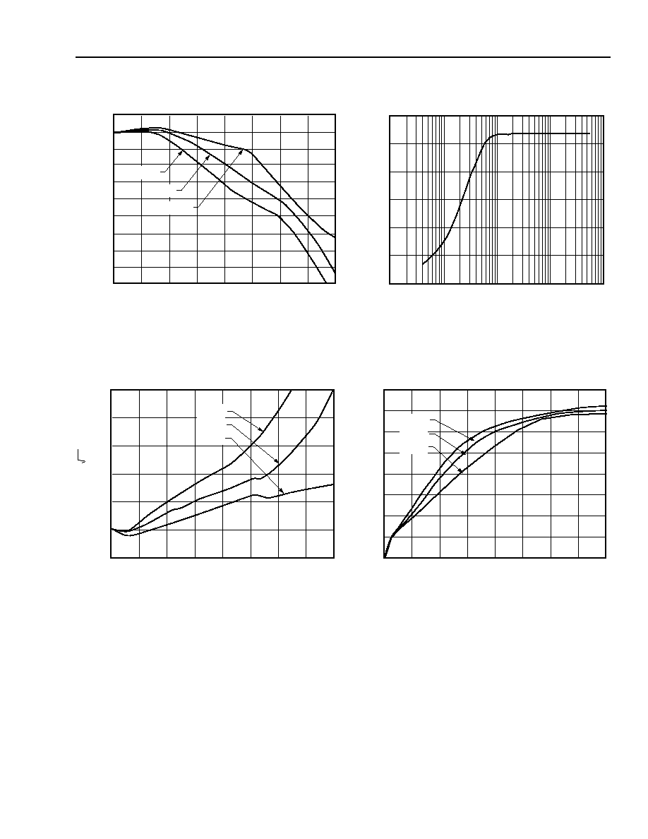
Characteristic Curves
(at T
A
= 25
∞
C, V
SS
= ≠5.2 V, C
DETECTOR
= 0.0 pF, 0.5 pF, 1.0 pF, R
LOAD
= 50
)
5-5330(F)r.1, 5-5331(F).ar2, 5-5332(F)r.2, 5-5333(F)r.2
1. >25 dB dynamic range requires an external Si dual operational amplifier. The detector polarity is such that current enters the LG1628A (i.e.,
the detector anode is connected to the LG1628A).
Figure 6. Characteristic Curves as Measured on the LG1628AXA Hybrid Integrated Circuit
A. Small-Signal Transimpedance
B. Overload Characteristics
1
C. Input Spectral Noise Density
D. Total Input Noise Current
30
25
20
15
10
5
0
0.0
0.5
1.0
1.5
2.0
2.5
3.0
3.5
4.0
FREQUENCY (GHz)
0.0 pF
1.0 pF
0.5 pF
SI
TOT
(pA/ Hz)
400
350
300
250
150
100
0
0.0
0.5
1.0
1.5
2.0
2.5
3.0
3.5
4.0
FREQUENCY (GHz)
I
TOT
(nArms)
0.0 pF
1.0 pF
0.5 pF
50
200
80
77
74
71
68
65
62
59
56
53
50
0
0.5
1.0
1.5
2.0
2.5
3.0
3.5
4.0
FREQUENCY (GHz)
TRANSIMPEDANCE (dB
)
1.0 pF
0.5 pF
0.0 pF
600
100
0
0.001
0.01
0.1
1
APD CURRENT (mAavg)
OUTPUT VOLTAGE (mVp-p)
200
300
400
500
10
LG1628AXA SONET/SDH 2.488 Gbits/s
Preliminary Data Sheet
Transimpedance Amplifier
January 1998
10
Lucent Technologies Inc.
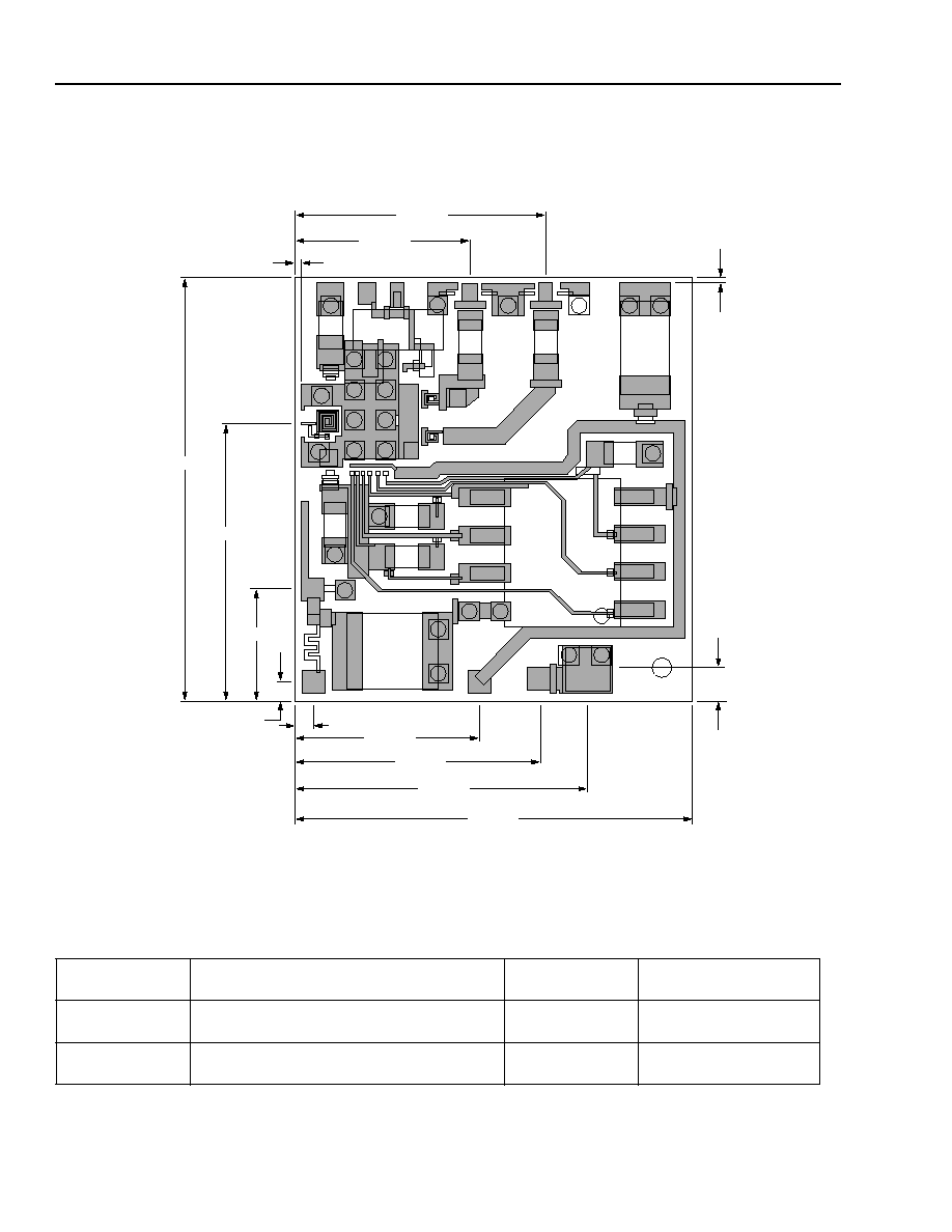
Dimensional Drawing of the Hybrid Integrated Circuit (HIC)
Dimensions are in inches. Ceramic thickness is 0.025 inches.
5-5336(F).ar3
Figure 7. HIC Dimensions and Location of Bonding Pads
Ordering Information
* Second output on BXA is terminated through to ground 50
on hybrid.
Device Code
Package
Temperature
Comcode
(Ordering Number)
LG1628AXA
Hybrid Integrated Circuit
Differential Output
0
∞
C to 85
∞
C
107791469
LG1628BXA*
Hybrid Integrated Circuit
Single-ended Output
0
∞
C to 85
∞
C
108052085
5
60x30 7
125x60
4
60x30
10
9
60x30
18
15
2
60x30
8
14
13
60X30
60X30
12
3
120X100
20
6
60X30
19
0.327
0.224
0.005
0.550
0.358
0.141
0.018
0.238
0.318
0.380
0.525
0.019
0.005
0.035
17
16

Preliminary Data Sheet
LG1628AXA SONET/SDH 2.488 Gbits/s
January 1998
Transimpedance Amplifier
11
Lucent Technologies Inc.
Notes

LG1628AXA SONET/SDH 2.488 Gbits/s
Preliminary Data Sheet
Interactive Terminal Transmission Convergence
January 1998
Lucent Technologies Inc. reserves the right to make changes to the product(s) or information contained herein without notice. No liability is assumed as a result of their use or application. No
rights under any patent accompany the sale of any such product(s) or information.
Copyright © 1998 Lucent Technologies Inc.
All Rights Reserved
Printed in U.S.A.
January 1998
DS97-156FCE
For additional information, contact your Microelectronics Group Account Manager or the following:
INTERNET:
http://www.lucent.com/micro
E-MAIL:
docmaster@micro.lucent.com
U.S.A.:
Microelectronics Group, Lucent Technologies Inc., 555 Union Boulevard, Room 30L-15P-BA, Allentown, PA 18103
1-800-372-2447, FAX 610-712-4106 (In CANADA: 1-800-553-2448, FAX 610-712-4106)
ASIA PACIFIC: Microelectronics Group, Lucent Technologies Singapore Pte. Ltd., 77 Science Park Drive, #03-18 Cintech III, Singapore 118256
Tel. (65) 778 8833, FAX (65) 777 7495
JAPAN:
Microelectronics Group, Lucent Technologies Japan Ltd., 7-18, Higashi-Gotanda 2-chome, Shinagawa-ku, Tokyo 141, Japan
Tel. (81) 3 5421 1600, FAX (81) 3 5421 1700
EUROPE:
Data Requests: MICROELECTRONICS GROUP DATALINE: Tel. (44) 1189 324 299, FAX (44) 1189 328 148
Technical Inquiries: GERMANY: (49) 89 95086 0 (Munich), UNITED KINGDOM: (44) 1344 865 900 (Bracknell),
FRANCE: (33) 1 41 45 77 00 (Paris), SWEDEN: (46) 8 600 7070 (Stockholm), FINLAND: (358) 9 4354 2800 (Helsinki),
ITALY: (39) 2 6601 1800 (Milan), SPAIN: (34) 1 807 1441 (Madrid)