 | –≠–ª–µ–∫—Ç—Ä–æ–Ω–Ω—ã–π –∫–æ–º–ø–æ–Ω–µ–Ω—Ç: LSP2916 | –°–∫–∞—á–∞—Ç—å:  PDF PDF  ZIP ZIP |
Preliminary Data Sheet
July 2001
LSP2916 16-Channel, High-Voltage Driver
Features
I
16 amplifier channels available in one package.
I
Outputs from 0 V to ≠298 V per channel.
I
Programmable output current limit (50
µA to
300
µA).
I
Fixed gain set by internal resistors. (The fixed gain
for version A is ≠32 V/V, and ≠66 V/V for version
B.)
I
Minimal external components.
Applications
I
Optical crosspoint switches.
I
Optical microelectromechanical systems (MEMS)
components.
Description
This LSP2916 16-channel, high-voltage (HV) driver
is targeted for microoptomechanical systems. Each
device contains 16 high-voltage amplifiers with an
output voltage range of 0 V to ≠298 V. Internal gain-
setting resistors provide a fixed gain of ≠32 V/V,
thereby minimizing external component count. Each
amplifier can output up to 300
µA, ideal for deflection
and control of optical MEMS mirrors. Output current
limit is programmed by an external resistor.
Additionally, careful attention was paid to minimizing
offset drift and gain variation over temperature. The
internal block diagram is shown in Figure 1. There
are two versions, version A (LSP2916A) and version
B (LSP2916B). For version A, R
F
= 8 M
and
R
IN
= 250 k
; and for version B, R
F
= 8.25 M
and
R
IN
= 125 k
. So LSP2916A has the fixed gain of
≠32 V/V and LSP2916B has the fixed gain of
≠66 V/V.
The LSP2916 requires one negative high-voltage
power supply (V
HN
) and one positive 5 V analog
power supply (V
LP
). Corresponding to the 16
channels, there are 16 negative input voltage pins,
≠INx (x = 1, 2, . . .
, 16), and the corresponding 16
output pins, OUTPUTx
(x = 1, 2, . . .
, 16).
+IN is the noninverting input for all 16 amplifiers,
which means all the amplifiers share the same
noninverting input. +IN should be connected to GND
for typical applications. I
BIAS
pin will set the current
limit for the amplifiers by connecting it to an external
resistor. The LSP2916 is available in a leaded
surface-mount 64-pin MQFP package.
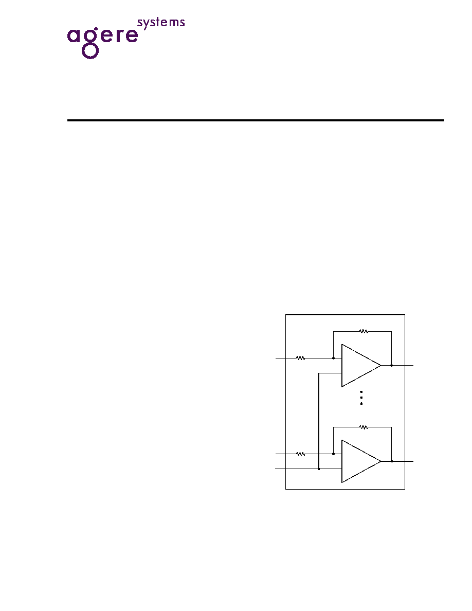
Block Diagram
1682(F)
Figure 1. LSP2916 Internal Functional Block
Diagram
R
IN
≠IN16
+IN
OUTPUT 16
R
F
R
IN
≠IN1
+
≠
OUTPUT 1
R
F
+
≠
LSP2916
2
2
Agere Systems Inc.
Preliminary Data Sheet
July 2001
LSP2916 16-Channel, High-Voltage Driver
Description
(continued)
Typical Application Circuit
1683(F)
Figure 2. Typical Application Circuit
OUTPUT 1
OUTPUT 16
MEMS
+
≠
+
≠
MATRIX
R
F
R
F
R
IN
R
IN
LSP2916
DAC
≠IN1
≠IN16
+IN
GND
Rib = 143 k
10
0.1
µF
0.1
µF
V
HN
V
LP
DAC
Agere Systems Inc.
3
Preliminary Data Sheet
July 2001
LSP2916 16-Channel, High-Voltage Driver
Pin Information
1541.a(F)
Figure 3. External Connections
Table 1. LSP2916 Pin Order
Pin
Number
Symbol
Pin
Number
Symbol
Pin
Number
Symbol
Pin
Number
Symbol
1
NC
17
OUTPUT8
33
NC
49
OUTPUT16
2
≠IN9
18
NC
34
≠IN1
50
NC
3
≠IN10
19
OUTPUT7
35
≠IN2
51
NC
4
≠IN11
20
NC
36
≠IN3
52
OUTPUT15
5
≠IN12
21
OUTPUT6
37
≠IN4
53
NC
6
NC
22
NC
38
GND
54
OUTPUT14
7
NC
23
OUTPUT5
39
V
LP
55
NC
8
NC
24
NC
40
I
BIAS
56
OUTPUT13
9
NC
25
OUTPUT4
41
NC
57
NC
10
NC
26
NC
42
NC
58
OUTPUT12
11
NC
27
OUTPUT3
43
+IN
59
NC
12
≠IN5
28
NC
44
≠IN13
60
OUTPUT11
13
≠IN6
29
OUTPUT2
45
≠IN14
61
NC
14
≠IN7
30
NC
46
≠IN15
62
OUTPUT10
15
≠IN8
31
OUTPUT1
47
≠IN16
63
NC
16
NC
32
V
HN
48
NC
64
OUTPUT9
NC
≠IN9
≠IN10
≠IN11
≠IN12
NC
NC
NC
NC
NC
NC
≠IN5
≠IN6
≠IN7
≠IN8
NC
1
2
3
4
5
6
7
8
9
10
11
12
13
14
15
16
NC
≠IN16
≠IN15
≠IN14
≠IN13
+IN
NC
NC
I
BIAS
V
LP
GND
≠IN4
≠IN3
≠IN2
≠IN1
NC
48
47
46
45
44
43
42
41
40
39
38
37
36
35
34
33
OU
T
P
UT
8
NC
OU
T
P
UT
7
NC
OU
T
P
UT
6
NC
OU
T
P
UT
5
NC
OU
T
P
UT
4
NC
OU
T
P
UT
3
NC
OU
T
P
UT
2
NC
OU
T
P
UT
1
V
HN
17
18
19
20
21
22
23
24
25
26
27
28
29
30
31
32
OUT
P
UT
16
NC
NC
OUT
P
UT
15
NC
OUT
P
UT
14
NC
OUT
P
UT
13
NC
OUT
P
UT
12
NC
OUT
P
UT
11
NC
OUT
P
UT
10
NC
OUT
P
UT
9
49
50
51
52
53
54
55
56
57
58
59
60
61
62
63
64
4
Agere Systems Inc.
Preliminary Data Sheet
July 2001
LSP2916 16-Channel, High-Voltage Driver
Pin Information
(continued)
Table 2. LSP2916 Pin Description
Pin Name
Function
Pin Total
Counts
Description
V
LP
Power Supply
1
5 V analog power supply.
GND
Ground
1
Analog ground.
V
HN
V
HN
< |≠298| V
1
High-voltage negative supply.
I
BIAS
Current Limit Control
1
Sets current limit with external resistor to GND.
+IN
Analog Input
1
Noninverting input for all channels.
≠INx
Analog Input
16
Inverting input for each channel.
OUTPUTx
Analog Output
16
Output.
Absolute Maximum Ratings
Stresses in excess of the absolute maximum ratings
can cause permanent damage to the device. These are
absolute stress ratings only. Functional operation of the
device is not implied at these or any other conditions in
excess of those given in the operational sections of the
data sheet. Exposure to absolute maximum ratings for
extended periods can adversely affect device reliability.
Table 3. Absolute Maximum Ratings
Handling Precautions
Although protection circuitry has been designed for this
device, proper precautions should be taken to avoid
exposure to electrostatic discharge (ESD) during
handling and mounting. Agere Systems Inc. employs a
human-body model (HMB) and charged-device model
(CDM) for ESD-susceptibility testing and protection
design evaluation. ESD voltage thresholds are
dependent on the circuit parameters used in the
defined model. No industry-wide standard has been
adopted for CDM. However, a standard HBM
(resistance = 1500
, capacitance = 100 pF) is widely
used, and therefore, can be used for comparison
purposes. The HBM ESD threshold (>500 V) presented
here was obtained by using these circuit parameters.
Application Notes
LSP2916 is recommended for MEMS optical systems.
It features programmable current limit while the output
can swing up to ≠298 V. With all the feedback resistors
inside the chip, there is
no more need for these resis-
tors in the external circuit.
Safety Handling for the High-Voltage Device
LSP2916 is designed to operate up to 298 V negative
power supply, so special care should be paid to safety
issues.
Bypass Capacitors/Protection Series Resistor for
the Power Supplies
To minimize noise coupling to the output, a 0.1
µ
F
bypass capacitor should be placed as close as
possible to all power supply pins. Additionally, to avoid
the possible degradation of the LSP2916 when V
HN
is
hot switched, a 10
series resistor between the V
HN
pin and the V
HN
power supply is required.
Parameter
Min
Typ
Max
Unit
Power Supply:
V
HN
V
LP
0
4.5
≠160.0
5.0
≠298.0
5.5
V
V
Operating Temperature
≠5
25
85
∞C
Storage Temperature
≠40
--
85
∞C
Ambient Temperature
≠5
25
70
∞C
Agere Systems Inc.
5
Preliminary Data Sheet
July 2001
LSP2916 16-Channel, High-Voltage Driver
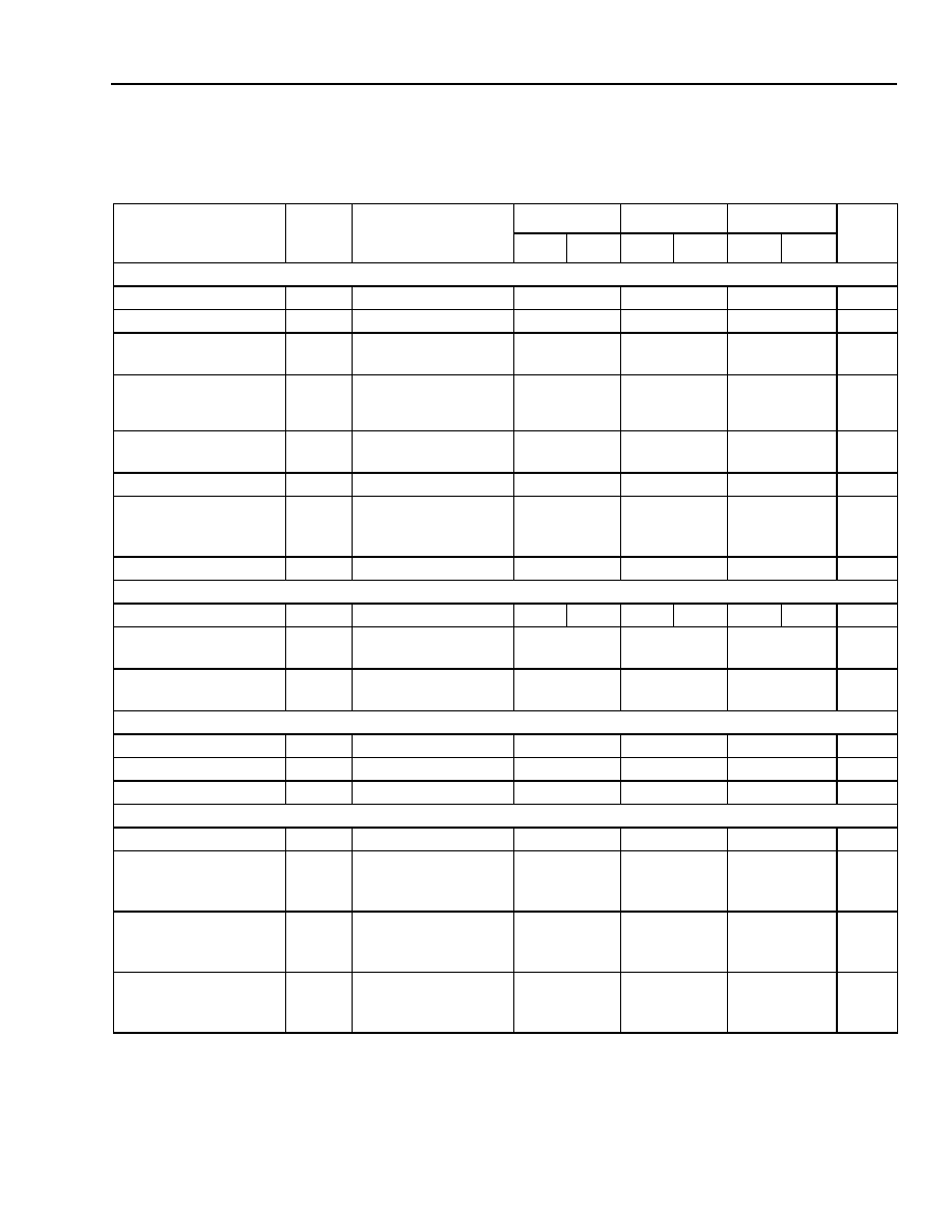
Electrical Characteristics
Table 4. Electrical Characteristics
T
A
= 25 ∞C, V
LP
= 5 V, V
HN
= ≠200 V, noninverting input +IN = 0 V, I
BIAS
resistor = 143 k
.
Parameters
Symbol
Condition
Min
Typ
Max
Unit
2916A 2916B 2916A 2916B 2916A 2916B
Input Characteristics
Input Resistance
R
≠
IN
= 5 V
125
200
500
k
Input Offset Voltage*
--
≠
IN
= 0 V
≠20
0
20
mV
Input Offset Voltage
Drift
--
≠
IN = 0 V
0 ∞C--70 ∞C
--
4
--
µV/∞C
Input Noise
--
f
10 kHz
C = 150 pF
R = 10 M
--
10.3
--
µVrms
Input Bias Current
I(≠IN
x)
≠
IN = 5 V
12.5
25
50
µA
Input Bias Current
I(+IN
)
≠
IN
= 5 V
≠40
0
40
nA
Power Supply
Rejection Ratio
PSRR
V
HN
V
LP
No load
No load
--
--
85
52
--
--
dB
dB
Input Range
≠
IN
--
≠0.5
--
10
V
Gain
Voltage Gain
G
≠
IN
= 3 mV
30.4
63.0
32.0
66.0
33.6
69.0
V/V
Gain Temperature
Coefficient
G
TC
--
--
≠1.25 x 10
≠5
--
--
Channel-to-Channel
Gain Match
--
--
--
2
--
%
Amplifier Output Characteristics
Output Resistance
--
--
10
90
125
k
Amplifier Current Limit
--
Rib = 143 k
85
100
115
µA
Output Voltage
--
--
V
HN
+ 2.5 V
--
V
LPD
≠
3 V
V
Dynamics Characteristics
≠3 dB Bandwidth
--
--
--
6.5
--
kHz
Slew Rate
Rising
Falling
--
Input pulse = 0 V--4 V
C = 150 pF and
R = 10 M
--
--
0.62
0.54
--
--
V/
µs
V/
µs
Settling Time
Rising
Falling
--
Input pulse = 0 V--4 V
C = 150 pF and
R = 10 M
--
--
277
309
--
--
µs
µs
Crosstalk
ß
Adjacent Channel
Nonadjacent Channel
--
--
C = 150 pF
f = 1 kHz
R = 16 M
--
--
≠71
≠80
--
--
dB
dB
*
Input offset voltage = (V
OFFSET
voltage/gain), the test condition is for the offset output voltage.
≠IN = 10 V.
≠IN
= ≠0.25 V.
ß Using an OP27 as buffer, test measurement was taken at the output of OP27.

6
Agere Systems Inc.
Preliminary Data Sheet
July 2001
LSP2916 16-Channel, High-Voltage Driver
Power Supply Currents at Room Temperature
Quiescent Current
I(V
HN
)
V
HN
= ≠160.0 V
V
LP
= 5.0 V
1.30
1.55
1.80
mA
I(V
LPA
)
1.36
1.60
1.85
mA
Power Consumption
P
V
HN
= ≠160.0 V
V
LP
= 5.0 V
--
256
--
mW
* Input offset voltage = (V
OFFSET
voltage/gain), the test condition is for the offset output voltage.
≠IN = 10 V.
≠IN = ≠0.25 V.
ß Using an OP27 as buffer, test measurement was taken at the output of OP27.
Electrical Characteristics
(continued)
Table 4. Electrical Characteristics (continued)
T
A
= 25 ∞C, V
LP
= 5 V, V
HN
= ≠200 V, noninverting input +IN = 0 V, I
BIAS
resistor = 143 k
.
Parameters
Symbol
Condition
Min
Typ
Max
Unit
2916A 2916B 2916A 2916B 2916A 2916B

Agere Systems Inc.
7
Preliminary Data Sheet
July 2001
LSP2916 16-Channel, High-Voltage Driver
Electrical Characteristics
(continued)
2286(F)
Note: Test conditions for the LSP2916A are: V
HN
= ≠200 V,
V
LP
= 5 V, R
ib
= 144 k
.
Figure 4. Current from V
HN
vs. Temperature
2287(F)
Note: Test conditions for the LSP2916A are: V
HN
= ≠200 V,
V
LP
= 5 V, R
ib
= 144 k
.
Figure 5. Current from V
LP
vs. Temperature
Output Current Range at Different
Resistance on Pin I
BIAS
Figure 6 shows the output current range when different
resistances are applied to pin I
BIAS
.
Test condition: maximum current limit is 300
µA.
Table 5. Output Current Range at Different
Resistances on I
BIAS
1686(F)
Figure 6. Resistor (Rib) vs. Output Current Limit
2285(F)
Note: Test conditions for the LSP2916A are: V
HN
= ≠200 V,
V
LP
= 5 V, R
ib
= 144 k
.
Figure 7. Gain vs. Output Voltage (V
HN
= ≠160 V)
2288(F)
Note: Test conditions for the LSP2916A are: V
HN
= ≠200 V,
V
LP
= 5 V, R
ib
= 144 k
.
Figure 8. ≠3 dB Plot
Resistance on I
BIAS
Min
Typ
Max
Unit
143 k
85
100
115
µA
70.3 k
170
200
230
µA
45.2 k
255
300
345
µA
-20 -10
0
10
20
30
1.4
1.45
1.5
1.55
1.6
1.65
CU
RRE
N
T
F
R
OM
V
HN
(mA
)
TEMPERATURE (∫C)
40
50
60
70
100 110
80
90
-20 -10
0
10
20
30
1.35
1.45
1.5
1.55
1.6
1.65
CU
RRE
N
T
F
R
OM
V
LP
(mA
)
TEMPERATURE (∫C)
40
50
60
70
100 110
80
90
1.4
350
300
250
200
150
100
50
0
0.25
0.2
0.15
0.1
0.05
CURRENT (mA)
0.3
Rib
(k
)
1.009
2
3.008
4.006
5.002
6.001
31.45
31.5
31.55
31.6
31.65
31.7
N
O
R
M
A
L
IZ
E
D
GA
IN
INPUT (V)
100 200 500 1000 2000 3000
0
0.4
0.6
0.8
1
1.2
NOR
M
A
L
IZ
E
D
OU
T
P
U
T
FREQUENCY (Hz)
4000 5000 5500 6000
8000
6500 7000
0.2
8
Agere Systems Inc.
Preliminary Data Sheet
July 2001
LSP2916 16-Channel, High-Voltage Driver
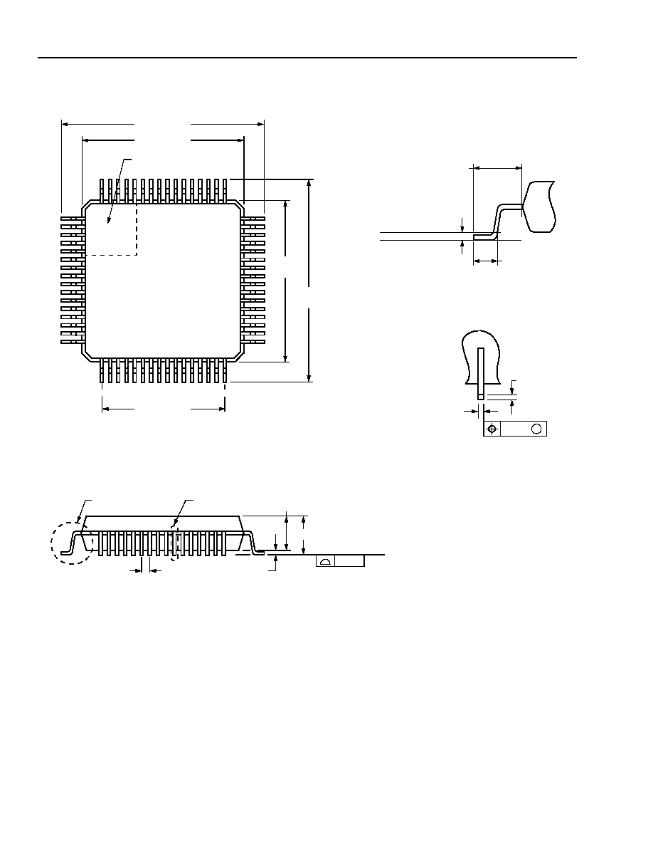
LSP2916AHA/LSP2916BHA Package Diagram
5-5202.a(F)
33
48
14.00
± 0.20
17.20
± 0.25
DETAIL A
DETAIL B
2.45 MAX
SEATING PLANE
0.10
1.80/2.20
0.25 MAX
1
16
49
64
PIN #1 IDENTIFIER ZONE
17.20
± 0.25
14.00
± 0.20
32
17
0.30/0.45
0.20
M
0.30/0.40
DETAIL B
0.25
0.73/1.03
1.60 REF
GAGE PLANE
SEATING PLANE
DETAIL A
0.80 BSC
12.00 REF

Agere Systems Inc.
9
Preliminary Data Sheet
July 2001
LSP2916 16-Channel, High-Voltage Driver
Ordering Information
Version
Device Code
Temperature Range
Package
LSP2916A
LSP2916AHA
0 ∞C--70 ∞C
64 MQFP
LSP2916B
LSP2916BHA
0 ∞C--70 ∞C
64 MQFP

Agere Systems Inc. reserves the right to make changes to the product(s) or information contained herein without notice. No liability is assumed as a result of their use or application.
Copyright © 2001 Agere Systems Inc.
All Rights Reserved
Printed in U.S.A.
July 2001
DS01-023ASP
For additional information, contact your Agere Systems Account Manager or the following:
INTERNET:
http://www.agere.com
E-MAIL:
docmaster@micro.lucent.com
N. AMERICA: Agere Systems Inc., 555 Union Boulevard, Room 30L-15P-BA, Allentown, PA 18109-3286
1-800-372-2447, FAX 610-712-4106 (In CANADA: 1-800-553-2448, FAX 610-712-4106)
ASIA PACIFIC: Agere Systems Singapore Pte. Ltd., 77 Science Park Drive, #03-18 Cintech III, Singapore 118256
Tel. (65) 778 8833, FAX (65) 777 7495
CHINA:
Agere Systems (Shanghai) Co., Ltd., 33/F Jin Mao Tower, 88 Century Boulevard Pudong, Shanghai 200121 PRC
Tel. (86) 21 50471212, FAX (86) 21 50472266
JAPAN:
Agere Systems Japan Ltd., 7-18, Higashi-Gotanda 2-chome, Shinagawa-ku, Tokyo 141, Japan
Tel. (81) 3 5421 1600, FAX (81) 3 5421 1700
EUROPE:
Data Requests: DATALINE: Tel. (44) 7000 582 368, FAX (44) 1189 328 148
Technical Inquiries:GERMANY: (49) 89 95086 0 (Munich), UNITED KINGDOM: (44) 1344 865 900 (Ascot),
FRANCE: (33) 1 40 83 68 00 (Paris), SWEDEN: (46) 8 594 607 00 (Stockholm), FINLAND: (358) 9 3507670 (Helsinki),
ITALY: (39) 02 6608131 (Milan), SPAIN: (34) 1 807 1441 (Madrid)