 | –≠–ª–µ–∫—Ç—Ä–æ–Ω–Ω—ã–π –∫–æ–º–ø–æ–Ω–µ–Ω—Ç: LSP2961 | –°–∫–∞—á–∞—Ç—å:  PDF PDF  ZIP ZIP |

Advance Data Sheet
September 2001
LSP2961
Precision Log Ratio Amplifier
Features
I
Seven decades (1 nA to 10 mA) typical input range
I
Internal scale factor K = 1 ± 2% (K externally
adjustable):
(eq.
1)
I
Internal trimmed reference current
(I
REF
= 1 µA ± 5%, externally adjustable)
I
Maximum ±100 mV output offset (externally
adjustable)
I
Minimal external components
I
±5 V power supply
I
TSSOP small package
Applications
I
Optical light density measurement
I
Log, log ratio computation
I
Data linearization
Description
The LSP2961 is a single-channel precision logarithm
and log ratio integrated circuit powered by +5 V and
≠5 V power supplies. The voltage output of the
amplifier is a logarithmic function of the ratio of a
reference current (I
REF
) over the input current (I
IN
).
The scale factor is set internally to 1 V/decade, and
is further adjustable by adding an external resistor.
The input dynamic range for the amplifier is a six-
decade (1 nA to 1 mA) minimum, with seven-decade
(1 nA to 10 mA) and eight-decade (100 pA to 10 mA)
operation available with increased conformity error.
The amplifier has an internal trimmed reference 1
µA
± 5% current source that is also externally adjustable
using an external resistor. The output offset voltage
is 100 mV maximum and can be nulled using an
external potentiometer.
The input current is applied to the IN pin and the
corresponding output is taken from the OUTPUT pin.
For a 1 V/decade application in a stable temperature
environment, no external components are required to
obtain the specified performance. For an application
that a scale factor other than 1 V/decade is required,
an external resistor connecting the SCALE FACTOR
pin to either the OUTPUT pin or GND will result in
less or more than 1 V/decade for the scale factor.
The amplifier's output can range from (V
CC
≠ 1 V) to
(V
EE
+ 1 V). This is ideal for the control in optical
density measurements, and in other situations such
as precision logarithm calculations. Each amplifier
has an internally trimmed reference current of 1
µA.
This reference current can be changed using an
external resistor connecting to the I
REF_ADJ
pin, and
either V
CC
or GND, depending on the need to
increase or decrease the reference current.
Additionally, the maximum output offset voltage is
±100 mV. This can be nulled using an external
potentiometer connected between the ±5 V supplies
and the wiper connected to the V
OS_ADJ
pin. The
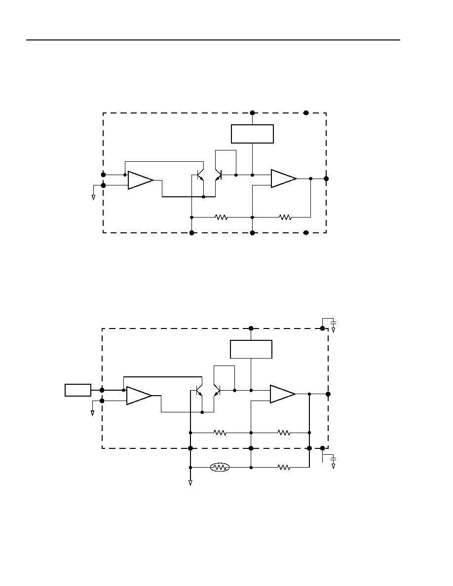
internal block diagram is shown in Figure 1.
The LSP2961 is available in a 3 mm x 3 mm TSSOP
package. The 8-pin LSP2961 requires one negative
5 V power supply (V
EE
) and one positive 5 V power
supply (V
CC
). Refer to Table 1 for detailed pin
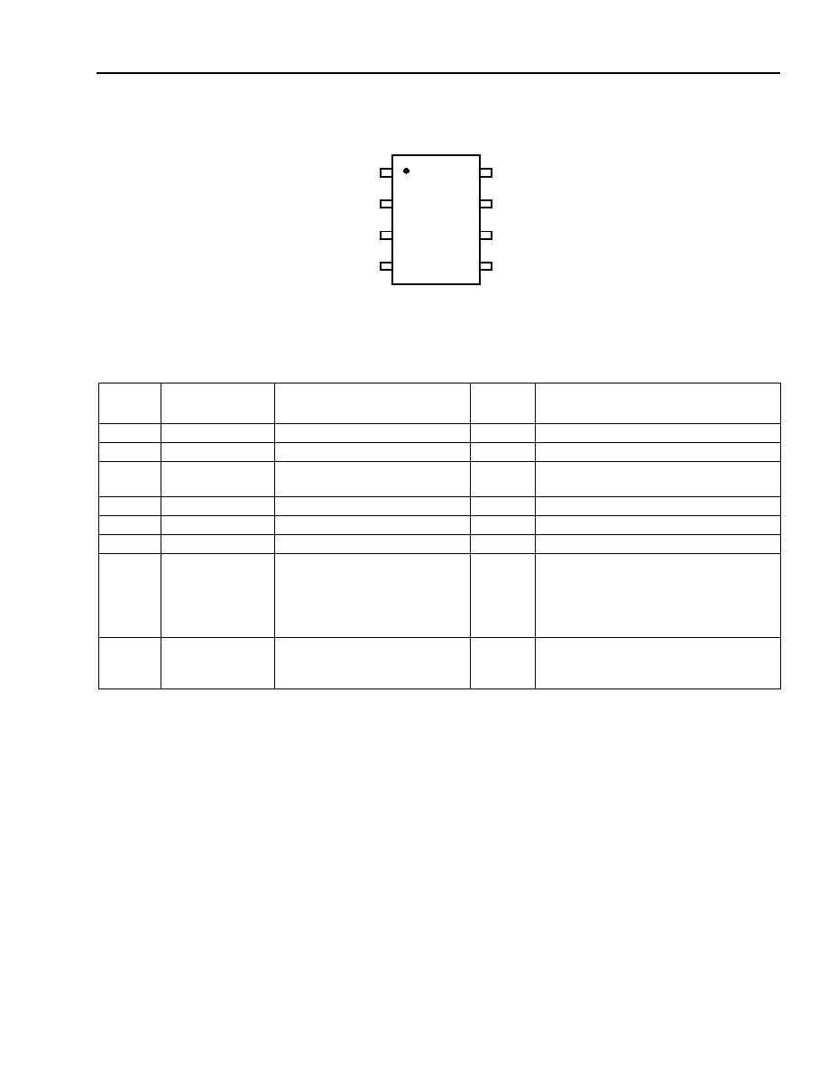
information. Figure 3 references the external pin
connections.
OUTPUT
K
I
REF
I
IN
-------------
log
◊
=

2
Agere Systems Inc.
Advance Data Sheet
September 2001
Precision Log Ratio Amplifier
LSP2961
Description
(continued)
Block Diagram
2352.a(F)
Figure 1. LSP2961 Internal Block Diagram
Typical Application Circuit
2353.b(F)
Figure 2. Typical Application Circuit with External Temperature Compensation
V
OS_ADJ
(8)
GND (2)
V
IN≠
V
IN+
REFERENCE
CURRENT
V
IN≠
V
IN+
OUTPUT (6)
IN
(1)
SCALE FACTOR (7)
10.2 k
160 k
I
REF_ADJ
(3)
V
CC
(5)
V
EE
(4)
µ
0.1 F
µ
0.1 F
V
OS_ADJ
(8)
V
IN≠
V
IN+
REFERENCE
CURRENT
V
IN≠
V
IN+
OUTPUT (6)
SCALE FACTOR (7)
10.2 k
160 k
I
REF_ADJ
(3)
V
CC
V
EE
PIN
1 k
16 k
(0.42%)
THERMISTOR
RESISTOR
GND (2)

Agere Systems Inc.
3
Advance Data Sheet
September 2001
Precision Log Ratio Amplifier
LSP2961
Pin Information
2311(F)
Figure 3. External Connections
Table 1. LSP2961 Pin Description
Pin
Number
Pin Name
Function
Pin Total
Counts
Description
1
IN
Input
1
Input current.
2
GND
Ground
1
Analog ground.
3
I
REF_ADJ
Sets the Reference Current to
Other than 1 µA
1
Used to set reference current with an
external resistor to GND or V
CC
.
4
V
EE
Power Supply
1
≠5 V power supply.
5
V
CC
Power Supply
1
5 V power supply.
6
OUTPUT
Output Voltage
1
Output voltage.
7
SCALE FACTOR Sets the Scale Factor to Other
than 1 V/decade
1
Used to change the scale factor to
other than 1 V/decade (either less than
or greater than) with an external
resistor connecting to the OUTPUT pin
or GND.
8
V
OS_ADJ
Offset Voltage Adjustment
1
Used to null offset voltage by
connecting to the wiper of an external
potentiometer between V
CC
and V
EE
.
V
OS_ADJ
SCALE
OUTPUT
V
CC
IN
I
REF_ADJ
V
EE
GND
FACTOR
1
3
4
2
8
6
5
7

4
Agere Systems Inc.
Advance Data Sheet
September 2001
Precision Log Ratio Amplifier
LSP2961
Absolute Maximum Ratings
Stresses in excess of the absolute maximum ratings can cause permanent damage to the device. These are
absolute stress ratings only. Functional operation of the device is not implied at these or any other conditions in
excess of those given in the operational sections of the data sheet. Exposure to absolute maximum ratings for
extended periods can adversely affect device reliability.
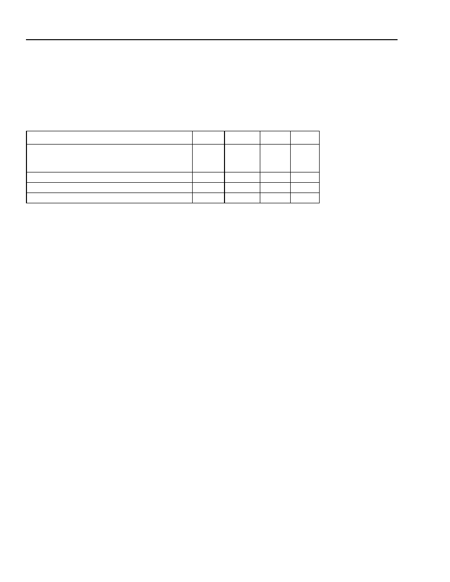
Table 2. Absolute Maximum Ratings
Handling Precautions
Although protection circuitry has been designed into this device, proper precautions should be taken to avoid
exposure to electrostatic discharge (ESD) during handling and mounting. Agere Systems employs a human-body
model (HBM) and charged-device model (CDM) for ESD-susceptibility testing and protection design evaluation.
ESD voltage thresholds are dependent on the circuit parameters used in the defined model. No industrywide
standard has been adopted for the CDM. However, a standard HBM (resistance = 1500
, capacitance = 100 pF)
is widely used and, therefore, can be used for comparison purposes. The HBM ESD threshold (>1500 V)
presented here was obtained by using these circuit parameters.
Application Considerations
A typical application is shown in Figure 2 for optical light intensity detection with temperature compensation by
using a thermistor with positive temperature coefficient of 0.42%.
Parameter
Min
Typ
Max
Unit
Power Supply
V
CC
V
EE
4.0
≠6.0
5.0
≠5.0
6.0
≠4.0
V
V
Operating Temperature (T
A
)
≠40
25
85
∞C
Storage Temperature
≠65
25
150
∞C
Lead Temperature (soldering 10 seconds)
--
--
300
∞C

Agere Systems Inc.
5
Advance Data Sheet
September 2001
Precision Log Ratio Amplifier
LSP2961
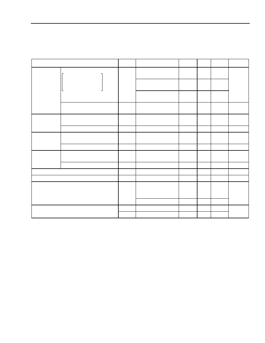
Electrical Characteristics
Table 3. Electrical Characteristics
T
A
= 25 ∞C, V
CC
= 5 V, V
EE
= ≠5 V, no external components for performance adjustment.
Note: Terms used for the specification of the analog log amplifier:
I
Total conformity error--this is used to describe the log linearity of the log amplifier, which is the maximum
deviation from the best-fit straight line of logarithm, allowing for offset error.
Parameter
Symbol
Conditions
Min
Typ
Max
Unit
Total
Conformity
Error
--
T
A
= 25 ∞C
IN = 1 nA to 1 mA
--
1
TBD
%
T
A
= 25 ∞C
IN = 1 nA to 10 mA
--
TBD
--
T
A
= 25 ∞C
IN = 100 pA to 10 mA
--
TBD
--
Temperature
Coefficient
1, 2
1. Can be externally compensated using a thermistor and a resistor.
--
≠5 ∞C to 70 ∞C
2
2. Guaranteed by design.
--
0.34
--
%/∞C
Scale Factor
3
3. Externally adjustable using a resistor.
Scale Factor
K
T
A
= 25 ∞C
IN = 1 nA to 1 mA
0.98
1
1.02
V/decade
Temperature Coefficient
2
--
≠5 ∞C to 70 ∞C
1
--
0.34
--
%/∞C
Reference
Accuracy
3
Reference
Accuracy
--
T
A
= 25 ∞C
IN = 1 nA to 1 mA
0.95
1
1.05
µA
Temperature Coefficient
2
--
≠5 ∞C to 70 ∞C
1
--
0.02
--
%/∞C
Output Offset
Voltage
4
4. Can be nulled using an external potentiometer.
--
V
OS
T
A
= 25 ∞C
IN = 1 nA to 1 mA
≠100
≠10
100
mV
Temperature Coefficient
2
--
≠5 ∞C to 70 ∞C
--
0.20
--
%/∞C
3 dB Bandwidth
5, 6
5. Transimpedance bandwidth.
6. Tested by limited samples.
f
3dB
C = 10 pF, IN = 1 µA
--
100
--
kHz
Output Voltage Range
--
--
V
EE
+ 1
--
V
CC
≠ 1
V
Supply Current
7
7. Supply current at 1 nA < IN
< 1 mA.
--
R
LOAD
> 1 M
IN = 1 nA to 1 mA
≠5 ∞C to 70
∞C
1
0.2
0.3
1.3
mA
IN
1 µA
8
8. Supply current at IN
1 µA.
0.18
0.24
0.3
Power Supply Operation Range
2
V
CC
--
4.5
5.0
5.5
V
V
EE
--
≠4.5
≠5.0
≠5.5
K
I
REF
I
IN
------------
log
◊
V
OUT
≠
V
FULLSCALE
---------------------------------------------------------
100
%
◊

Copyright © 2001 Agere Systems Inc.
All Rights Reserved
September 2001
DS01-188ASP
Agere Systems Inc. reserves the right to make changes to the product(s) or information contained herein without notice. No liability is assumed as a result of their use or application.
For additional information, contact your Agere Systems Account Manager or the following:
INTERNET:
http://www.agere.com
E-MAIL:
docmaster@agere.com
N. AMERICA: Agere Systems Inc., 555 Union Boulevard, Room 30L-15P-BA, Allentown, PA 18109-3286
1-800-372-2447, FAX 610-712-4106 (In CANADA: 1-800-553-2448, FAX 610-712-4106)
ASIA:
Agere Systems Hong Kong Ltd., Suites 3201 & 3210-12, 32/F, Tower 2, The Gateway, Harbour City, Kowloon
Tel. (852) 3129-2000, FAX (852) 3129-2020
CHINA: (86) 21-5047-1212 (Shanghai), (86) 10-6522-5566 (Beijing), (86) 755-695-7224 (Shenzhen)
JAPAN: (81) 3-5421-1600 (Tokyo), KOREA: (82) 2-767-1850 (Seoul), SINGAPORE: (65) 778-8833, TAIWAN: (886) 2-2725-5858 (Taipei)
EUROPE:
Tel. (44) 7000 624624, FAX (44) 1344 488 045
Advance Data Sheet
September 2001
Precision Log Ratio Amplifier
LSP2961
LSP2961 Package Diagram
0790(F)
0.40/0.70
0.10
C
4
1
5
8
4.90 BSC
1.10 MAX
0.127/0.25
0.65
BSC
0.25/0.40
SEATING PLANE
0.13/0.23
2.90/3.10
0.75/0.95
0∞/6∞
1
2.90/3.10
0.60
0.60
0.50

