
Preliminary Data Sheet
July 2000
LU3X31T-T64 Single-Port 3 V
10/100 Ethernet Transceiver TX
Overview
The LU3X31T-T64 is a fully integrated
10/100 Mbits/s physical layer device with an inte-
grated transceiver. It is provided in a 64-pin TQFP
package with low-power operation and powerdown
modes. Typical applications for this part are CardBus
and PCMCIA Ethernet products. Operating at 3.3 V,
the LU3X31T-T64 is a powerful device for the forward
migration of legacy 10 Mbits/s products and noncom-
pliant (does not have autonegotiation) 100 Mbits/s
devices. The LU3X31T-T64 was designed from the
beginning to conform fully with all pertinent specifica-
tions, from the
ISO
*
/IEC 11801 and
EIA
/TIA 568
cabling guidelines to
ANSI
X3.263 TP-PMD to
IEEE
ß
802.3 Ethernet specifications.
Features
s
Single-chip integrated physical layer and trans-
ceiver for 10Base-T and/or 100Base-T functions
s
IEEE
802.3 compatible 10Base-T and 100Base-T
physical layer interface and
ANSI
X3.263 TP-PMD
compatible transceiver
s
Built-in analog 10 Mbits/s receive filter, eliminating
the need for external filters
s
Built-in 10 Mbits/s transmit filter
s
10 Mbits/s PLL exceeding tolerances for both pre-
amble and data jitter
s
100 Mbits/s PLL, combined with the digital adap-
tive equalizer, robustly handles variations in rise-
fall time, excessive attenuation due to channel
loss, duty-cycle distortion, crosstalk, and baseline
wander
s
Transmit rise-fall time can be manipulated to pro-
vide lower emissions, amplitude fully compatible
for proper interoperability
s
Programmable scrambler seed for better FCC
compliancy
s
IEEE
802.3u Clause 28 compliant autonegotiation
for full 10 Mbits/s and 100 Mbits/s control
s
Fully configurable via pins and management
accesses
s
Extended management support with interrupt
capabilities
s
PHY MIB support
s
Symbol mode option
s
Low-power operation: <150 mA max
s
Low autonegotiation power: <30 mA
s
Very low powerdown mode: <5 mA
s
64-pin TQFP package (10 mm x 10 mm x 1.4 mm)
*
ISO
is a registered trademark of The International Organization
for Standardization.
EIA
is a registered trademark of The Electronic Industries Asso-
ciation.
ANSI
is a registered trademark of The American National Stan-
dards Institute, Inc.
ß
IEEE
is a registered trademark of The Institute of Electrical and
Electronics Engineers, Inc.

Table of Contents
Contents
Page
LU3X31T-T64 Single-Port 3 V
Preliminary Data Sheet
10/100 Ethernet Transceiver TX
July 2000
2
Lucent Technologies Inc.
Overview................................................................................................................................................................... 1
Features ................................................................................................................................................................... 1
Pin Descriptions........................................................................................................................................................ 6
Functional Description ............................................................................................................................................ 10
Media Independent Interface (MII) ...................................................................................................................... 10
100Base-X Module.............................................................................................................................................. 11
100Base-X Receiver ........................................................................................................................................... 14
100Base-X Link Monitor ...................................................................................................................................... 15
100Base-TX Transceiver..................................................................................................................................... 16
10Base-T Module ................................................................................................................................................ 16
Clock Synthesizer................................................................................................................................................ 18
Autonegotiation ................................................................................................................................................... 18
Reset Operation .................................................................................................................................................. 19
100Base-X PCS Configuration............................................................................................................................ 20
MII Registers .......................................................................................................................................................... 21
dc and ac Specifications......................................................................................................................................... 31
Absolute Maximum Ratings................................................................................................................................. 31
Clock Timing........................................................................................................................................................... 32
Outline Diagram...................................................................................................................................................... 43
64-Pin TQFP ....................................................................................................................................................... 43
Ordering Information............................................................................................................................................... 44
Tables
Page
Table 1. Twisted-Pair Magnetic Interface ................................................................................................................. 5
Table 2. Twisted-Pair Transceiver Control ................................................................................................................ 6
Table 3. MII Interface ............................................................................................................................................... 6
Table 4. PHY Address Configuration ....................................................................................................................... 7
Table 5. 100Base-X PCS Configuration................................................................................................................... 7
Table 6. Autonegotiation Configuration .................................................................................................................... 7
Table 7. LED and Status Outputs ............................................................................................................................ 8
Table 8. Clock and Chip Reset ................................................................................................................................ 9
Table 9. Power and Ground ..................................................................................................................................... 9
Table 10. Symbol Code Scrambler ........................................................................................................................ 13
Table 11. Autonegotiation ...................................................................................................................................... 20
Table 12. MII Management Registers .................................................................................................................... 20
Table 13. Control Register (Register 0h) ............................................................................................................... 21
Table 14. Status Register (Register 1h)................................................................................................................. 23
Table 15. PHY Identifier (Register 2h) ................................................................................................................... 25
Table 16. PHY Identifier (Register 3h) ................................................................................................................... 25
Table 17. Autonegotiation Advertisement (Register 4h) ........................................................................................ 25
Table 18. Autonegotiation Link Partner Ability (Register 5h) ................................................................................. 25
Table 19. Autonegotiation Expansion Register (Register 6h) ................................................................................ 26
Table 20. Receive Error Counter (Register 15h).................................................................................................... 26
Table 21. PHY Control/Status Register (Register 17h).......................................................................................... 27
Table 22. Config 100 Register (Register 18h)........................................................................................................ 28
Table 23. PHY Address Register (Register 19h) ................................................................................................... 29
Table 24. Config 10 Register (Register 1Ah) ......................................................................................................... 29
Table 25. Status 100 Register (Register 1Bh) ....................................................................................................... 30
Table 26. Status 10 Register (Register 1Ch) ......................................................................................................... 30

Table of Contents
(continued)
Tables
(continued)
Page
Preliminary Data Sheet
LU3X31T-T64 Single-Port 3 V
July 2000
10/100 Ethernet Transceiver TX
Lucent Technologies Inc.
3
Table 27. Interrupt Mask Register (Register 1Dh).................................................................................................. 30
Table 28. Interrupt Status Register (Register 1Eh) ................................................................................................ 31
Table 29. Absolute Maximum Ratings.................................................................................................................... 31
Table 30. Operating Conditions.............................................................................................................................. 31
Table 31. dc Characteristics................................................................................................................................... 32
Table 32. System Clock (Xin) ................................................................................................................................. 32
Table 33. Transmit Clock (Input and Output) .......................................................................................................... 33
Table 34. Management Clock................................................................................................................................. 34
Table 35. MII Receive Timing................................................................................................................................. 35
Table 36. MII Transmit Timing ................................................................................................................................ 36
Table 37. Transmit Timing ...................................................................................................................................... 37
Table 38. Receive Timing....................................................................................................................................... 38
Table 39. Reset and Configuration Timing ............................................................................................................. 39
Table 40. PMD Characteristics............................................................................................................................... 40
Figures
Page
Figure 1. LU3X31T-T64 Block Diagram ................................................................................................................... 4
Figure 2. Pin Diagram .............................................................................................................................................. 5
Figure 3. 100Base-X Data Path ............................................................................................................................. 12
Figure 4. 10Base-T Module Data Path .................................................................................................................. 16
Figure 5. Hardware Reset Configurations.............................................................................................................. 19
Figure 6. System Timing ........................................................................................................................................ 32
Figure 7. Transmit Timing (Input and Output) ........................................................................................................ 33
Figure 8. Management Timing ............................................................................................................................... 34
Figure 9. MII Receive Timing ................................................................................................................................. 35
Figure 10. MII Transmit Timing .............................................................................................................................. 36
Figure 11. Transmit Timing .................................................................................................................................... 37
Figure 12. Receive Timing ..................................................................................................................................... 38
Figure 13. Reset and Configuration Timing ........................................................................................................... 39
Figure 14. PMD Timing .......................................................................................................................................... 40
Figure 15. Connection Diagrams (Frequency References).................................................................................... 41
Figure 16. Connection Diagrams (10/100BTX Operation) ..................................................................................... 42
LU3X31T-T64 Single-Port 3 V
Preliminary Data Sheet
10/100 Ethernet Transceiver TX
July 2000
4
Lucent Technologies Inc.
Features
(continued)
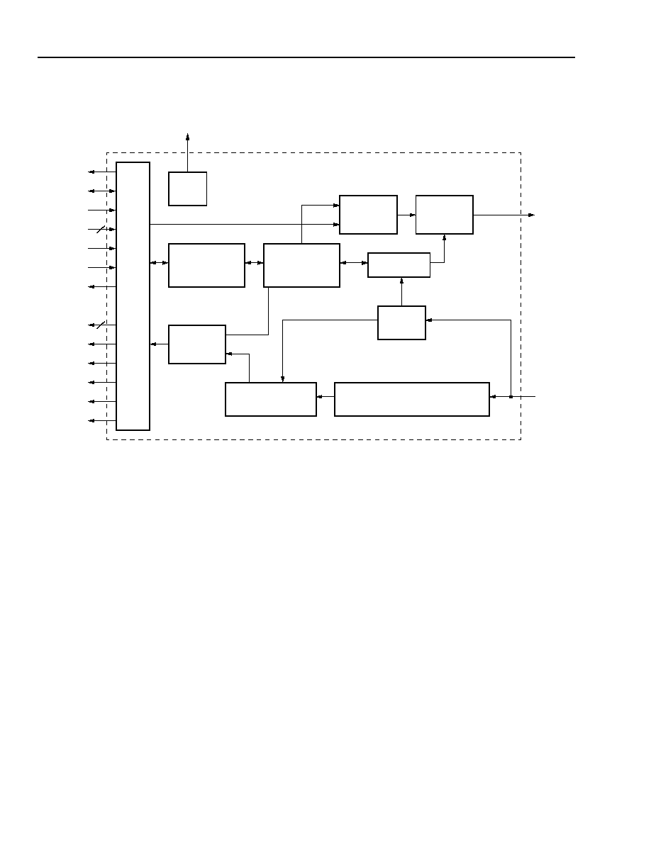
5-6779(F).ar.2
Figure 1. LU3X31T-T64 Block Diagram
MI
I
INTE
RFA
C
E
LO
GIC
LED
S
LED
S
MANAGEMENT
INTERFACE
REGISTER/
CONFIG/
CONTROL
10/100-RX
PCS
10/100-TX
PCS
10/100-TX
DRIVERS
AUTONEG
RX10
SQUELCH
CLOCK SYNTHESIS
AND RECOVERY
ADAPTIVE EQUALIZER
BASELINE WANDER CORRECTION
MDIO
MDC
TXD
TXEN
TXER
TXCLK
RXD
RXDV
RXER
RXCLK
COL
CRS
MDIOINTZ
TPTX
±
TPRX
±
Lucent Technologies Inc.
5
Preliminary Data Sheet
LU3X31T-T64 Single-Port 3 V
July 2000
10/100 Ethernet Transceiver TX
Features
(continued)
5-6780(F).br.5
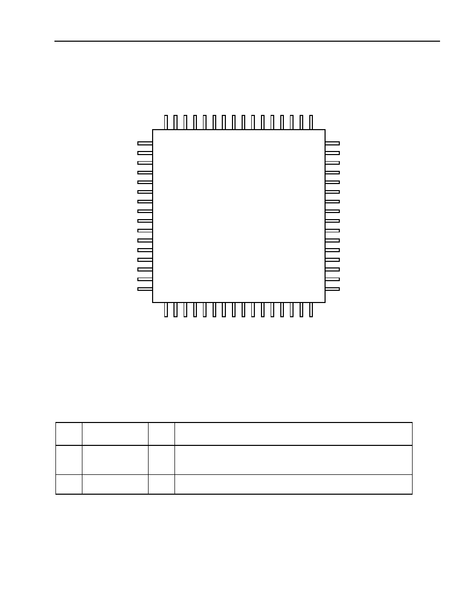
Figure 2. Pin Diagram
Table 1. Twisted-Pair Magnetic Interface
Pin
No.
Pin Name
I/O
Pin Description
53
54
TPTX+
TPTX≠
O
Twisted-Pair Transmit Driver Pair. These pins are used to transmit
100Base-T MLT-3 signals on Category 5 UTP cable or 10Base-T
Manchester signals on Category 3 UTP cable.
61
62
TPRX+
TPRX≠
I
Twisted-Pair Receive Pair. These pins receive 100Base-T MLT 3 or
10Base-T Manchester data.
1
2
3
4
5
6
7
8
9
10
11
13
14
15
16
17
18
19
20
21
22
23
24
25
26
27
28
29
30
31
32
TX
D0
TX
D1
TX
D2
TX
D3
TX
ER
TX
EN
GND8
V
DD
8
RX
CLK
RXD0
RXD1
RXD2
RXD3
RX
ER
RX
DV
LEDS
P/10FDEN
XOUT
XIN
XTLV
DD
MDC
LNKLED/BPALIGN
LEDFD/10HDEN
LEDCOL/BP4B5B
LEDTX/ACTLED/BPSCR
LEDRX
COL/PHY[4]
V
DD
6
V
DD
4
GND4
MDIO
CRS/PHY[3]
TXCLK
RE
F
1
0
TX
V
DD
1
TX
GND1
TP
TX
+
TP
TX
≠
TX
V
DD
2
CS
G
N
D
CS
V
DD
CS
V
DD
RX
V
DD
1
RX
G
N
D1
TP
RX+
TP
RX≠
RX
G
N
D2
RX
V
DD
2
RESV
100FDEN
GND9
AUTONEN
TPTXTR
EQGND1
EQV
DD
1
RESV
RSTZ
PHY[0]
GND1
V
DD
1
MDIOINTZ/PHY[2]
100HDEN
V
DD
5
12
PHY[1]
48
47
46
45
44
43
42
41
40
39
38
36
35
34
33
37
64
63
62
61
60
59
58
57
56
55
54
53
52
51
50
49
RE
F
100

LU3X31T-T64 Single-Port 3 V
Preliminary Data Sheet
10/100 Ethernet Transceiver TX
July 2000
6
Lucent Technologies Inc.
Pin Descriptions
Table 2. Twisted-Pair Transceiver Control
Table 3. MII Interface
Note: Smaller font indicates that the pin has multiple functions.
Pin
No.
Pin Name
I/O
Pin Description
50
REF100
I
Reference Resistor for 100 Mbits/s Twisted-Pair Driver. Connect
this pin to ground through a 301
resistor.
49
REF10
I
Reference Resistor for 10 Mbits/s Twisted-Pair Driver. Connect
this pin to ground through a 4.64 k
resistor.
5
TPTXTR
I
Twisted-Pair Transmitter 3-State. A high on this pin will 3-state the
twisted-pair outputs. Tie to ground in normal operation.
Pin
No.
Pin Name
I/O
Pin Description
18
RXDV
O
Receive Data Valid. Signals the presence of data on RXD[3:0].
19
RXER
O
Receive Error. Indicates a received coding error has occurred.
20
RXD3
O
Receive Data[3].
21
RXD2
O
Receive Data[2].
22
RXD1
O
Receive Data[1].
23
RXD0
O
Receive Data[0].
24
RXCLK
O
Receive Clock.
27
TXEN
I
Transmit Enable. Signals the presence of data on TXD[3:0].
28
TXER
I
Transmit Error. Indicates a transmit coding error has occurred.
29
TXD3
I
Transmit Data[3].
30
TXD2
I
Transmit Data[2].
31
TXD1
I
Transmit Data[1].
32
TXD0
I
Transmit Data[0].
33
TXCLK
O
Transmit Clock.
34
CRS/
PHY[3]
I/O
Carrier Sense/PHY Address[3]. This output pin indicates the carrier
sense condition. See Table 4 for PHY[3] description.
39
COL/
PHY[4]
I/O
Collision/False Carrier Sense. This output pin indicates collision
condition in normal MII operation and is squelch jabber in 10 Mbits/s
mode. See Table 4 for PHY[4] description.
35
MDIO
I/O
Management Data I/O. Serial access to device config registers.
45
MDC
I
Management Data Clock. Clock for R/W of device config registers.
16
MDIOINTZ/
PHY[2]
I/O
MDIO Interrupt (Active-Low). The MDIO interrupt pin outputs a logic
0 pulse of 40 ns, synchronous to XIN, whenever an unmasked inter-
rupt condition is detected. Refer to management registers 1Dh and
1Eh for interrupt conditions. See Table 4 for PHY[2] description.

Lucent Technologies Inc.
7
Preliminary Data Sheet
LU3X31T-T64 Single-Port 3 V
July 2000
10/100 Ethernet Transceiver TX
Pin Descriptions
(continued)
Table 4. PHY Address Configuration
Note: Smaller font indicates that the pin has multiple functions.
Table 5. 100Base-X PCS Configuration
Note: Smaller font indicates that the pin has multiple functions.
Table 6. Autonegotiation Configuration (Refer to Table 11.)
Pin
No.
Pin Name
I/O
Pin Description
10
12
16
34
39
PHY[0]
PHY[1]
PHY[2]/
MDIOINTZ
PHY[3]/
CRS
PHY[4]/
COL
I
I
I/O
I/O
I/O
PHY Address[4:0]. These 5 pins are detected during powerup or reset to
initialize the PHY address used for MII management register interface. PHY
address 00h forces the PHY into MII isolate mode. PHY address pins[4:2]
have an internal 40 k
pull-down resistor. See Table 3 for MDIOINTZ, CRS,
and COL description.
Pin
No.
Pin Name
I/O
Pin Description
41
BPSCR/
LEDTX
/
ACTLED
I/O
Bypass Scrambler Mode. A high value on this pin during powerup or reset
will bypass the scramble/descramble operations in 100Base-X data path.
This pin has an internal 40 k
pull-down resistor. See Table 7 for LEDTX/
ACTLED description.
42
BP4B5B/
LEDCOL
I/O
Bypass 4B/5B Mode. A high value on this pin during powerup or reset will
bypass the 4B/5B encoder of the PHY. This pin has an internal 40 k
pull-
down resistor. See Table 7 for LEDCOL description.
44
BPALIGN/
LNKLED
I/O
Bypass Alignment Mode. A high value on this pin during powerup or reset
will bypass the alignment feature of the PHY. This bypass mode provides a
symbol interface. This pin has an internal 40 k
pull-down. See Table 7 for
LNKLED description.
Pin
No.
Pin Name
I/O
Pin Description
4
AUTONEN
I
Autonegotiation Enable. A high value on this pin during powerup or reset
will enable autonegotiation; a low value will disable it.
2
100FDEN
I
100 Full-Duplex Enable. The logic level of this pin is detected at powerup
or reset to determine whether 100 Mbits/s full-duplex mode is available.
When autonegotiation is enabled, this input sets the ability register bit in
advertisement register 4. When autonegotiation is not enabled, this input
will select the mode of operation.
11
100HDEN
I
100 Half-Duplex Enable. The logic level of this pin is detected at powerup
or reset to determine whether 100 Mbits/s half-duplex mode is available.
When autonegotiation is enabled, this input sets the ability register bit in
advertisement register 4. When autonegotiation is not enabled, this input
will select the mode of operation.
17
10FDEN/
LEDSP
I/O
10 Full-Duplex Enable. The logic level of this pin is detected at
powerup or reset to determine whether 10 Mbits/s full-duplex mode is avail-
able. When autonegotiation is enabled, this input sets the ability register bit
in advertisement register 4. When autonegotiation is not enabled, this input
will select the mode of operation. This pin has an internal 40 k
pull-up
resistor. See Table 7 for LEDSP description.
Note: Smaller font indicates that the pin has multiple functions.

LU3X31T-T64 Single-Port 3 V
Preliminary Data Sheet
10/100 Ethernet Transceiver TX
July 2000
8
Lucent Technologies Inc.
Note: Smaller font indicates that the pin has multiple functions.
Table 7. LED and Status Outputs
Note: Smaller font indicates that the pin has multiple functions.
43
10HDEN/
LEDFD
I/O
10 Half-Duplex Enable. The logic level of this pin is detected at powerup or
reset to determine whether 10 Mbits/s half-duplex mode is available. When
autonegotiation is enabled, this input sets the ability register bit in advertise-
ment register 4. When autonegotiation is not enabled, this input will select
the mode of operation. This pin has an internal 40 k
pull-up resistor. See
Table 7 for LEDFD description.
Pin
No.
Pin Name
I/O
Pin Description
40
LEDRX
I/O
Receive LED. This output will drive a 10 mA LED if the LU3X31T-T64 is
receiving data from the UTP cable. This pin has an internal 40 k
pull-down
resistor. The LED should be connected as logic 0 configuration as shown in
Figure 5, without the 10 k
resistor.
41
LEDTX/ACTLED/
BPSCR
I/O
Transmit LED or Activity LED. When bit 7 of register 17h is 0, this output
will drive a 10 mA LED if the LU3X31T-T64 is transmitting data. If the control
bit is set, then the LED will be driven whenever receive or transmit activity is
present. This pin has an internal 40 k
pull-down. The LED should be con-
nected as LOGIC 0 configuration in Figure 5 without the 10 k
resistor. See
Table 5 for BPSCR description.
44
LNKLED/
BPALIGN
I/O
Link LED. This output will drive a 10 mA LED for as long as a valid link
exists across the cable. Place a 10 k
resistor across the LED pins if setting
to nondefault mode, i.e., bypass align mode as shown in Figure 5. See Table
5 for BPALIGN description.
42
LEDCOL/
BP4B5B
I/O
Collision LED. This output will drive a 10 mA LED whenever the LU3X31T-
T64 senses a collision has occurred. Place a 10 k
resistor across the LED
pins if setting to nondefault mode, i.e., bypass 4B/5B mode as shown in Fig-
ure 5. See Table 5 for BP4B5B description.
43
LEDFD/
10HDEN
I/O
Full-Duplex Status. This output will drive a 10 mA LED when the LU3X31T-
T64 is in full-duplex mode. Place a 10 k
resistor across the LED pins if set-
ting to nondefault mode, i.e., 10HD disable mode as shown in Figure 5. See
Table 6 for 10HDEN description.
17
LEDSP/
10FDEN
I/O
Speed Status. This output will drive a 10 mA LED when the LU3X31T-T64
is in 100 Mbits/s mode. Place a 10 k
resistor across the LED pins if setting
to nondefault mode, i.e., 10FD disable mode as shown in Figure 5. See
Table 6 for 10FDEN description.
Pin
No.
Pin Name
I/O
Pin Description
Pin Descriptions
(continued)
Table 6. Autonegotiation Configuration (Refer to Table 11.) (continued)

Lucent Technologies Inc.
9
Preliminary Data Sheet
LU3X31T-T64 Single-Port 3 V
July 2000
10/100 Ethernet Transceiver TX
Pin Descriptions
(continued)
Table 8. Clock and Chip Reset
Table 9. Power and Ground
Pin
No.
Pin Name
I/O
Pin Description
47
XIN
I
Crystal Oscillator Input or Clock Input. See Figure 15 for a con-
nection diagram.
48
XOUT
O
Crystal Oscillator Feedback Output. If a single-ended external
clock is connected to XIN pin, then XOUT should be grounded for
minimum power consumption. See Figure 15 for a connection dia-
gram.
9
RSTZ
I
Reset (Active-Low). This input must be held low for a minimum of
1 ms to reset the LU3X31T-T64.
1
8
RESV
--
Reserved. These pins are unused inputs and should be tied to
ground.
Plane
V
CC
Pin
Associated Ground Pin
Name
Pin Number
Name
Pin Number
RX Analog
RXV
DD
1
RXV
DD
2
59
64
RXGND1
RXGND2
60
63
TX Analog
TXV
DD
1
TXV
DD
2
51
55
TXGND1
--
52
--
CS
CSV
DD
CSV
DD
57
58
CSGND
--
56
--
Digital
V
DD
1
V
DD
4
V
DD
5
V
DD
6
V
DD
8
--
EQV
DD
1
15
37
13
38
25
--
7
GND1
GND4
--
--
GND8
GND9
EQGND1
14
36
--
--
26
3
6
Clock
XTLV
DD
46
--
--

10
Lucent Technologies Inc.
LU3X31T-T64 Single-Port 3 V
Preliminary Data Sheet
10/100 Ethernet Transceiver TX
July 2000
Functional Description
The LU3X31T-T64 integrates a 100Base-X physical
sublayer (PHY), a 100Base-TX physical medium
dependent (PMD) transceiver, and a complete 10Base-
T module into a single chip for both 10 Mbits/s and
100 Mbits/s Ethernet operation. This device provides
an
IEEE
802.3u compliant media independent interface
(MII) to communicate between the physical signaling
and the medium access control (MAC) layers for both
100Base-X and 10Base-T operations. The device is
capable of operating in either full-duplex mode or half-
duplex mode in either 10 Mbits/s or 100 Mbits/s opera-
tion. Operational modes can be selected by hardware
configuration pins, selected by software settings of
management registers, or determined by the on-chip
autonegotiation logic.
The 10Base-T section of the device consists of the
10 Mbits/s transceiver module with filters and a
Manchester ENDEC module.
The 100Base-X section of the device implements the
following functional blocks:
s
100Base-X physical coding sublayer (PCS)
s
100Base-X physical medium attachment (PMA)
s
Twisted-pair transceiver
The 100Base-X and 10Base-T sections share the fol-
lowing functional blocks:
s
Clock synthesizer module (CSM)
s
MII registers
s
IEEE
802.3u autonegotiation
Each of these functional blocks is described below.
Media Independent Interface (MII)
The LU3X31T-T64 implements an
IEEE
802.3u Clause
22 compliant MII as described below.
Interface Signals
Transmit Data Interface. The MII transmit data inter-
face comprises seven signals: TXD[3:0] are the nibble
size data path, TXEN signals the presence of data on
TXD, TXER indicates that a transmit coding error has
occurred, and TXCLK is the transmit clock that syn-
chronizes all the transmit signals. TXCLK is supplied by
the on-chip clock synthesizer.
Receive Data Interface. The MII receive data interface
comprises seven signals: RXD[3:0] are the nibble size
data path, RXDV signals the presence of data on RXD,
RXER indicates a received coding error, and RXCLK is
the receive clock. Depending upon the operation mode,
RXCLK is generated by the clock recovery module of
either the 100Base-X or 10Base-T receiver.
Status Interface. Two status signals, COL and CRS,
are generated in the LU3X31T-T64 to indicate collision
status and carrier sense status to the MAC. COL is
asserted asynchronously whenever LU3X31T-T64 is
transmitting and receiving at the same time in a half-
duplex operation mode. In the full-duplex mode, COL is
inactive. CRS is asserted asynchronously whenever
there is activity on either the transmitter or the receiver.
In full-duplex mode, CRS is asserted only when there is
activity on the receiver.
Operation Modes
The LU3X31T-T64 supports three operation modes
and an isolate mode as described below.
100 Mbits/s Mode. For 100 Mbits/s operation, the MII
operates in nibble mode with a clock rate of 25 MHz. In
normal operation, the MII data at RXD[3:0] and
TXD[3:0] are 4 bits wide. In bypass mode (either
BYP_4B5B or BYP_ALIGN option selected), the MII
data takes the form of 5-bit code-groups. The least sig-
nificant 4 bits appear on TXD[3:0] and RXD[3:0] as
usual, and the most significant bits (TXD[4] and
RXD[4]) appear on the TXER and RXER pins, respec-
tively.
10 Mbits/s Mode. For 10 Mbits/s operation, the TXCLK
and RXCLK operate at 2.5 MHz. The data paths are
always 4 bits wide using TXD[3:0] and RXD[3:0] signal
lines.

Lucent Technologies Inc.
11
Preliminary Data Sheet
LU3X31T-T64 Single-Port 3 V
July 2000
10/100 Ethernet Transceiver TX
Functional Description
(continued)
MII Isolate Mode. The LU3X31T-T64 implements an
MII isolate mode that is controlled by bit 10 of the con-
trol register (register 0h). The LU3X31T-T64 will set this
bit to one if the PHY address is set to 00000 upon pow-
erup/hardware reset. Otherwise, the LU3X31T-T64 will
initialize this bit to 0. Setting this bit to a 1 will put the
LU3X31T-T64 into isolate mode.
The isolate mode can also be activated by setting the
PHY address (bits 15 through 11 of register 19h) to 0
through the serial management interface, although the
content of the isolate register is not affected by the
modification of PHY address.
The LU3X31T-T64 does not respond to packet data
present at TXD[3:0], TXEN, and TXER inputs and pre-
sents a high impedance on the TXCLK, RXCLK, RXDV,
RXER, RXD[3:0], COL, and CRS outputs. The
LU3X31T-T64 will continue to respond to all manage-
ment transactions.
Serial Management Interface
The serial management interface (SMI) is the part of
the MII that is used to control and monitor status of the
LU3X31T-T64. This mechanism corresponds to the MII
specification for 100Base-X (Clause 22) and supports
registers 0 through 6. Additional vendor-specific regis-
ters are implemented within the range of 16 to 31. All
the registers are described in MII Registers on page 21
of this data sheet.
Management Register Access. The SMI consists of
two pins, management data clock (MDC) and manage-
ment data input/output (MDIO). The LU3X31T-T64 is
designed to support an MDC frequency ranging up to
the
IEEE
specification of 2.5 MHz. The MDIO line is bi-
directional and may be shared by up to 32 devices.
The MDIO pin requires a 1.5 k
pull-up resistor which,
during IDLE and turnaround periods, will pull MDIO to
a logic 1 state. Each MII management data frame is
64 bits long. The first 32 bits are preamble consisting of
32 contiguous logic 1 bits on MDIO and 32 correspond-
ing cycles on MDC. Following preamble is the start-of-
frame field indicated by a <01> pattern. The next field
signals the operation code (OP): <10> indicates READ
from MII management register operation, and <01>
indicates WRITE to MII management register opera-
tion. The next two fields are PHY device address and
MII management register address. Both of them are
5 bits wide, and the most significant bit is transferred
first.
During READ operation, a 2-bit turnaround (TA) time
spacing between register address field and data field is
provided for the MDIO to avoid contention. Following
the turnaround time, a 16-bit data stream is read from
or written into the MII management registers of the
LU3X31T-T64.
The LU3X31T-T64 supports a preamble suppression
mode as indicated by a 1 in bit 6 of the basic mode sta-
tus register (BMSR, address 01h). If the station man-
agement entity (i.e., MAC or other management
controller) determines that all PHYs in the system sup-
port preamble suppression by returning a 1 in this bit,
then the station management entity need not generate
preamble for each management transaction. The
LU3X31T-T64 requires a single initialization sequence
of 32 bits of preamble following powerup/hardware
reset. This requirement is generally met by the manda-
tory pull-up resistor on MDIO or the management
access made to determine whether preamble suppres-
sion is supported. While the LU3X31T-T64 will respond
to management accesses without preamble, a mini-
mum of one idle bit between management transactions
is required as specified in
IEEE
802.3u.
The PHY device address for LU3X31T-T64 is stored in
the PHY address register (register address 19h). It is
initialized by the five I/O pins designated as PHY[4:0]
during powerup or hardware reset and can be changed
afterward by writing into register address 19h.
MDIO Interrupt. The LU3X31T-T64 implements inter-
rupt capability that can be used to notify the manage-
ment station of certain events. It generates an active-
high interrupt signal on the MDIOINTZ output pin
whenever one of the interrupt status registers (register
address 1Eh) becomes set while its corresponding
interrupt mask register (register address 1Dh) is
unmasked. Reading the interrupt status register (regis-
ter 1Eh) shows the source of the interrupt and clears
the interrupt output signal.
In addition to the MDIOINTZ pin, the LU3X31T-T64 can
also support the interrupt scheme used by the
TI Thun-
derLAN
*
MAC. This option can be enabled by setting
bit 11 of register 17h. Whenever this bit is set, the inter-
rupt is signaled through both the MDIOINTZ pin and
embedded in the MDIO signal.
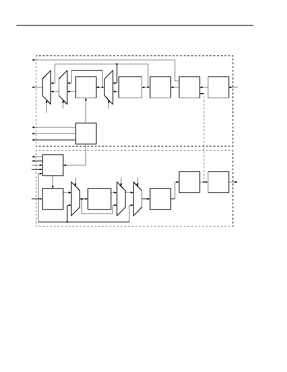
100Base-X Module
The LU3X31T-T64 implements a 100Base-X compliant
PCS and PMA and 100Base-TX compliant TP-PMD as
illustrated in Figure 3. Bypass options for each of the
major functional blocks within the 100Base-X PCS pro-
vides flexibility for various applications. 100 Mbits/s
PHY loopback is included for diagnostic purposes.
*
TI
is a registered trademark and
ThunderLAN
is a trademark of
Texas Instruments, Inc.
12
Lucent Technologies Inc.
LU3X31T-T64 Single-Port 3 V
Preliminary Data Sheet
10/100 Ethernet Transceiver TX
July 2000
Functional Description
(continued)
5-6781(F).ar.2
Figure 3. 100Base-X Data Path
EQUALIZER
CLOCK
RECOVERY
SERIAL
TO
PARALLEL
DE-
SCRAMBLER
5B/4B
DECODE
RECEIVE
STATE
MACHINE
TRANSMIT
STATE
MACHINE
4B/5B
ENCODE
SCRAMBLER
PARALLEL
TO
SERIAL
MLT-3
STATE
MACHINE
10/100
TRANSMIT
DRIVER
TPRX
±
TPTX
±
100 Mbit PHY
LOOPBACK PATH
BYP-SCR
BYP-4B5B
BYP-ALIGN
RXCLK
RXD[3:0]
CRS
RXDV
RXER
100BASE-X RECEIVER
100BASE-X TRANSMITTER
COL
TXCLK
TXEN
TXER
TXD[3:0]
BYP-4B5B
BYP-SCR
BYP-ALIGN
100Base-X Transmitter
The 100Base-X transmitter consists of functional
blocks which convert synchronous 4-bit nibble data, as
provided by the MII, to a 125 Mbits/s serial data
stream. The LU3X31T-T64 implements the 100Base-X
transmit state machine as specified in the
IEEE
802.3u
Standard, Clause 24 and comprises the following func-
tional blocks in its data path:
s
Symbol encoder
s
Scrambler block
s
Parallel/serial converter and NRZ/NRZI encoder
block
Symbol Encoder. The symbol encoder converts 4-bit
(4B) nibble data generated by the MAC into 5-bit (5B)
symbols for transmission. This conversion is required
to allow control symbols to be combined with DATA
symbols. Refer to the table below for 4B to 5B symbol
mapping.
Following onset of the TXEN signal, the 4B/5B symbol
encoder replaces the first two nibbles of the preamble
from the MAC frame with a /J/K code-group pair (11000
10001) start-of-stream delimiter (SSD). The symbol
encoder then replaces subsequent 4B codes with cor-
responding 5B symbols. Following negation of the
TXEN signal, the encoder substitutes the first two IDLE
symbols with a /T/R code-group pair (01101 00111)
end-of-stream delimiter (ESD) and then continuously
injects IDLE symbols into the transmit data stream until
the next transmit packet is detected.

Lucent Technologies Inc.
13
Preliminary Data Sheet
LU3X31T-T64 Single-Port 3 V
July 2000
10/100 Ethernet Transceiver TX
Functional Description
(continued)
Assertion of the TXER input while the TXEN input is
also asserted will cause the LU3X31T-T64 to substitute
HALT code-groups for the 5B code derived from data
present at TXD[3:0]. However, the SSD (/J/K) and ESD
(/T/R) will not be substituted with HALT code-groups.
Hence, the assertion of TXER while TXEN is asserted
will result in a frame properly encapsulated with the /J/
K and /T/R delimiters which contains HALT code-
groups in place of the DATA code-groups.
The 100 Mbits/s symbol decoder translates all invalid
code groups into 0Eh by default. In case the ACCEPT
HALT register is set (bit 5 of register 18h), the HALT
code-group (00100) is translated into 05h instead.
Table 10. Symbol Code Scrambler
Symbol
Name
5B Code
[4:0]
4B Code
[3:0]
Interpretation
0
11110
0000
DATA 0
1
01001
0001
DATA 1
2
10100
0010
DATA 2
3
10101
0011
DATA 3
4
01010
0100
DATA 4
5
01011
0101
DATA 5
6
01110
0110
DATA 6
7
01111
0111
DATA 7
8
10010
1000
DATA 8
9
10011
1001
DATA 9
A
10110
1010
DATA A
B
10111
1011
DATA B
C
11010
1100
DATA C
D
11011
1101
DATA D
E
11100
1110
DATA E
F
11101
1111
DATA F
I
11111
undefined
IDLE: interstream fill code
J
11000
0101
First start-of-stream delimiter
K
10001
0101
Second start-of-stream delimiter
T
01101
undefined
First end-of-stream delimiter
R
00111
undefined
Second end-of-stream delimiter
H
00100
undefined
HALT: transfer error
V
00000
undefined
Invalid code
V
00001
undefined
Invalid code
V
00010
undefined
Invalid code
V
00011
undefined
Invalid code
V
00101
undefined
Invalid code
V
00110
undefined
Invalid code
V
01000
undefined
Invalid code
V
01100
undefined
Invalid code
V
10000
undefined
Invalid code
V
11001
undefined
Invalid code

14
Lucent Technologies Inc.
LU3X31T-T64 Single-Port 3 V
Preliminary Data Sheet
10/100 Ethernet Transceiver TX
July 2000
Functional Description
(continued)
Scrambler. For 100Base-TX applications, the scram-
bler is required to control the radiated emissions at the
media connector and on the twisted-pair cable.
The LU3X31T-T64 implements a data scrambler as
defined by the TP-PMD stream cipher function. The
scrambler uses an 11-bit ciphering linear feedback shift
register (LFSR) with the following recursive linear func-
tion:
X[n] = X[n ≠ 11] + X[n ≠ 9] (modulo 2)
The output of the LFSR is combined with the 5B data
from the symbol encoder via an exclusive-OR logic
function. By scrambling the data, the total energy
launched onto the cable is randomly distributed over a
wide frequency range.
A seed value for the scrambler function can be loaded
by setting bit 4 of register 18h. When this bit is set, the
content of bits 10 though 0 of register 19h, which con-
sists of the 5-bit PHY address and a 6-bit user seed,
will be loaded into the LFSR. By specifying unique
seed value for each PHY in a system, the total EMI
energy produced by a repeater application can be
reduced.
Parallel-to-Serial & NRZ-to-NRZI Conversion. After
the transmit data stream is scrambled, the 5-bit code-
group is loaded into a shift register and clocked out with
a 125 MHz clock into a serial bit stream. The serialized
data is further converted from NRZ to NRZI format,
which produces a transition on every logic 1 and no
transition on logic 0.
Collision Detect. During 100 Mbits/s half-duplex oper-
ation, a collision condition is indicated if the transmitter
and receiver become active simultaneously. A collision
condition is indicated by the COL pin (pin 39). For full-
duplex applications, the COL signal is never asserted.
A collision test register exists at address 0, bit 7.
100Base-X Receiver
The 100Base-X receiver consists of functional blocks
required to recover and condition the 125 Mbits/s
receive data stream. The LU3X31T-T64 implements
the 100Base-X receive state machine diagram as given
in
ANSI
/
IEEE
Standard 802.3u, Clause 24. The
125 Mbits/s receive data stream originates from in a
100Base-TX application.
The receiver block consists of the following functional
blocks:
s
Clock recovery module
s
NRZI/NRZ and serial/parallel decoder
s
Descrambler
s
Symbol alignment block
s
Symbol decoder
s
Collision detect block
s
Carrier sense block
s
Stream decoder block
Clock Recovery. The clock recovery module accepts
125 Mbits/s scrambled NRZI data stream from either
the on-chip 100Base-TX receiver or from an external
100Base-FX transceiver. The LU3X31T-T64 uses an
onboard digital phase-locked loop (PLL) to extract clock
information of the incoming NRZI data, which is then
used to retime the data stream and set data bound-
aries.
After power-on or reset, the PLL locks to a free-running
25 MHz clock derived from the external clock source.
When initial lock is achieved, the PLL switches to lock
to the data stream, extracts a 125 MHz clock from the
data, and uses it for bit framing of the recovered data.
NRZI-to-NRZ & Serial-to-Parallel Conversion. The
recovered data is converted from NRZI to NRZ and
then to a 5-bit parallel format for the LU3X31T-T64
descrambler. The 5-bit parallel data is not necessarily
aligned to 4B/5B code-group's boundary.
Data Descrambling. The scrambled data is presented
in groups of 5 bits (quints) to a deciphering circuit that
reverses the data scrambling process performed by the
transmitter. The descrambler acquires synchronization
with the data stream by recognizing IDLE bursts of 40
or more bits and locking its deciphering linear feedback
shift register (LFSR) to the state of the scrambling
LFSR. Upon achieving synchronization, the incoming
data is XORed by the deciphering LFSR and descram-
bled, again in groups of 5 bits (quints).
In order to maintain synchronization, the descrambler
continuously monitors the validity of the unscrambled
data that it generates. To ensure this, a link state moni-
tor and a hold timer are used to constantly monitor the
synchronization status. Upon synchronization of the
descrambler, the hold timer starts a 722
µ
s countdown.

Lucent Technologies Inc.
15
Preliminary Data Sheet
LU3X31T-T64 Single-Port 3 V
July 2000
10/100 Ethernet Transceiver TX
Functional Description
(continued)
Upon detection of sufficient IDLE symbols within the
722
µ
s period, the hold timer will reset and begin a new
countdown. This monitoring operation will continue
indefinitely given a properly operating network connec-
tion with good signal integrity. If the link state monitor
does not recognize sufficient unscrambled IDLE sym-
bols within the 722
µ
s period, the entire descrambler
will be forced out of the current state of synchronization
and reset in order to reacquire synchronization. Regis-
ter 18h, bit 3, can be used to extend the timer to
2000
µ
s.
Symbol Alignment. The symbol alignment circuit in
the LU3X31T-T64 determines code word alignment by
recognizing the /J/K delimiter pair. This circuit operates
on unaligned 5-bit data from the descrambler and is
capable of finding /J/K at any of the five possible start-
ing positions within the descrambled data quints. Once
the /J/K symbol pair (11000 10001) is detected, subse-
quent data is aligned on a fixed boundary.
Symbol Decoding. The symbol decoder functions as
a look-up table that translates incoming 5B symbols
into 4B nibbles. The symbol decoder first detects the
/J/K symbol pair preceded by IDLE symbols and
replaces the symbol with MAC preamble. All subse-
quent 5B symbols are converted to the corresponding
4B nibbles for the duration of the entire packet. This
conversion ceases upon the detection of the /T/R sym-
bol pair denoting the end of stream delimiter (ESD).
The translated data is presented on the RXD[3:0] sig-
nal lines with RXD[0] representing the least significant
bit of the translated nibble.
Valid Data Signal. The valid data signal (RXDV) indi-
cates that recovered and decoded nibbles are being
presented on the RXD[3:0] outputs synchronous to
RXCLK. RXDV is asserted when the first nibble of
translated /J/K is ready for transfer over the media
independent interface (MII). It remains active until
either the /T/R delimiter is recognized, link test indi-
cates failure, or no signal is detected. On any of these
conditions, RXDV is deasserted.
Receiver Errors. The RXER signal is used to commu-
nicate receiver error conditions. While the receiver is in
a state of holding RXDV asserted, the RXER will be
asserted for each code word that does not map to a
valid code-group.
100Base-X Link Monitor
The 100Base-X link monitor function allows the
receiver to ensure that reliable data is being received.
Without reliable data reception, the link monitor will halt
both transmit and receive operations until such time
that a valid link is detected.
The LU3X31T-T64 performs the link integrity test as
outlined in
IEEE
100Base-X (Clause 24) link monitor
state diagram. The link status is multiplexed with the
10 Mbits/s link status to form the reportable link status
bit in serial management register 1. This status also
drives the LNKLED pin.
When persistent signal energy is detected on the net-
work, the logic moves into a Link-Ready state, after
approximately 500
µ
s, and waits for an enable from the
autonegotiation module. When received, the link-up
state is entered, and the transmit and receive logic
blocks become active. Should autonegotiation be dis-
abled, the link integrity logic moves immediately to the
link-up state after entering the link-ready state.
Carrier Sense. Carrier sense (CRS) for 100 Mbits/s
operation is asserted upon the detection of two non-
contiguous zeros occurring within any 10-bit boundary
of the receive data stream.
The carrier sense function is independent of symbol
alignment. For 100 Mbits/s half-duplex operation, CRS
is asserted during either packet transmission or recep-
tion. For 100 Mbits/s full-duplex operation, CRS is
asserted only during packet reception. When the IDLE
symbol pair is detected in the receive data stream,
CRS is deasserted.
Bad SSD Detection. A bad start of stream delimiter
(Bad SSD) is an error condition that occurs in the
100Base-X receiver if carrier is detected (CRS
asserted) and a valid /J/K set of code groups (SSD) is
not received.
If this condition is detected, then the LU3X31T-T64 will
assert RXER and present RXD[3:0] = 1110 to the MII
for the cycles that correspond to received 5B code-
groups until at least two IDLE code groups are
detected. Once at least two IDLE code groups are
detected, RXER and CRS become deasserted.
16
16
Lucent Technologies Inc.
LU3X31T-T64 Single-Port 3 V
Preliminary Data Sheet
10/100 Ethernet Transceiver TX
July 2000
Functional Description
(continued)
100Base-TX Transceiver
LU3X31T-T64 implements a TP-PMD compliant trans-
ceiver for 100Base-TX operation. The differential trans-
mit driver is shared by the 10Base-T and 100Base-TX
subsystems. This arrangement results in one device
that uses the same external magnetics for both the
10Base-T and the 100Base-TX transmission with sim-
ple RC component connections. The individually wave-
shaped 10Base-T and 100Base-TX transmit signals
are multiplexed in the transmit output driver.
Transmit Drivers
The LU3X31T-T64 100Base-TX transmit driver imple-
ments MLT-3 translation and wave-shaping functions.
The rise/fall time of the output signal is closely con-
trolled to conform to the target range specified in the
ANSI
TP-PMD standard.
Twisted-Pair Receiver
For 100Base-TX operation, the incoming signal is
detected by the on-chip twisted-pair receiver that com-
prises the differential line receiver, an adaptive equal-
izer, and baseline wander compensation circuits.
The LU3X31T-T64 uses an adaptive equalizer which
changes filter frequency response in accordance with
cable length. The cable length is estimated based on
the incoming signal strength. The equalizer tunes itself
automatically for any cable length to compensate for
amplitude and phase distortions incurred from the
cable.
10Base-T Module
The 10Base-T Transceiver Module is
IEEE
802.3 com-
pliant. It includes the receiver, transmitter, collision,
heartbeat, loopback, jabber, waveshaper, and link
integrity functions, as defined in the standard. Figure 4
provides an overview for the 10Base-T module.
The LU3X31T-T64 10Base-T module is comprised of
the following functional blocks:
s
Manchester encoder and decoder
s
Collision detector
s
Link test function
s
Transmit driver and receiver
s
Serial and parallel interface
s
Jabber and SQE test functions
s
Polarity detection and correction
5-6782(F)r3
Figure 4. 10Base-T Module Data Path
FILTER
RECEIVE
10BASE-T
SMART
CLOCK
WAVE
10/100
FILTER
SQUELCH
RECOVERY
RECEIVE
PCS
10BASE-T
TRANSMIT
PCS
TRANSMIT
DRIVER
SHAPER
RXCLK
CRS
RXD[3:0]
COL
TXEN
TXER
TXD[3:0]
TXCLK
10 Mbit PHY
LOOPBACK
PATH
TPRX
±
TPTX
±
RXDV

Lucent Technologies Inc.
17
Preliminary Data Sheet
LU3X31T-T64 Single-Port 3 V
July 2000
10/100 Ethernet Transceiver TX
Functional Description
(continued)
Operation Modes
The LU3X31T-T64 10Base-T module is capable of
operating in either half-duplex mode or full-duplex
mode. In half-duplex mode, the LU3X31T-T64 functions
as an
IEEE
802.3 compliant transceiver with fully inte-
grated filtering. The COL pin signals collision, and the
CRS is asserted during transmit and receive. In full-
duplex mode, the LU3X31T-T64 can simultaneously
transmit and receive data.
Manchester Encoder/Decoder. Data encoding and
transmission begins when the transmit enable input
(TXEN) goes high and continues as long as the trans-
ceiver is in good link state. Transmission ends when the
transmit enable input goes low. The last transition
occurs at the center of the bit cell if the last bit is a 1, or
at the boundary of the bit cell if the last bit is 0.
Decoding is accomplished by a differential input
receiver circuit and a phase-locked loop that separates
the Manchester-encoded data stream into clock signals
and NRZ data. The decoder detects the end of a frame
when no more midbit transitions are detected. Within
one and a half bit times after the last bit, carrier sense
is deasserted.
Transmit Driver and Receiver. LU3X31T-T64 inte-
grates all the required signal conditioning functions in
its 10Base-T block such that external filters are not
required. Only an isolation transformer and impedance
matching resistors are needed for the 10Base-T trans-
mit and receive interface. The internal transmit filtering
ensures that all the harmonics in the transmit signal are
attenuated properly.
Smart Squelch. The smart squelch circuit is responsi-
ble for determining when valid data is present on the
differential receive. The LU3X31T-T64 implements an
intelligent receive squelch on the TPRX
±
differential
inputs to ensure that impulse noise on the receive
inputs will not be mistaken for a valid signal. The
squelch circuitry employs a combination of amplitude
and timing measurements (as specified in the
IEEE
802.3 10Base-T standard) to determine the validity of
data on the twisted-pair inputs.
The signal at the start of the packet is checked by the
analog squelch circuit, and any pulses not exceeding
the squelch level (either positive or negative, depend-
ing upon polarity) will be rejected. Once this first
squelch level is overcome correctly, the opposite
squelch level must then be exceeded within 150 ns.
Finally, the signal must exceed the original squelch
level within a further 150 ns to ensure that the input
waveform will not be rejected.
Only after all of these conditions have been satisfied
will a control signal be generated to indicate to the
remainder of the circuitry that valid data is present.
Valid data is considered to be present until the squelch
level has not been generated for a time longer than
200 ns, indicating end of packet. Once good data has
been detected, the squelch levels are reduced to mini-
mize the effect of noise causing premature end of
packet detection. The receive squelch threshold level
can be lowered for use in longer cable applications.
This is achieved by setting bit 11 or register address
1Ah.
Carrier Sense. Carrier sense (CRS) is asserted due to
receive activity once valid data is detected via the
smart squelch function.
For 10 Mbits/s half-duplex operation, CRS is asserted
during either packet transmission or reception.
For 10 Mbits/s full-duplex operation, the CRS is
asserted only on receive activity. CRS is deasserted
following an end of packet.
Collision Detection. For half-duplex operation, a
10Base-T collision is detected when the receive and
transmit channels are active simultaneously. Collisions
are reported by the COL signal. If the ENDEC is trans-
mitting when a collision is detected, the COL signal
remains set for the duration of the collision.
SQE Test Function. Approximately 1
µ
s after the
transmission of each packet, a signal quality error
(SQE) signal of approximately 10 bit times is generated
(internally) to indicate successful transmission. SQE is
reported as a pulse on the COL signal. This function
can be disabled by setting bit 12 of register 1Ah. The
SQE test function is disabled in full-duplex mode.
Jabber Function. The jabber function monitors the
LU3X31T-T64's output and disables the transmitter if it
attempts to transmit a longer than legal-sized packet. If
TXEN is high for greater than 24 ms, the 10Base-T
transmitter will be disabled and COL will go high.
Once disabled by the jabber function, the transmitter
stays disabled for the entire time that the TXEN signal
is asserted. This signal has to be deasserted for
approximately 256 ms (the unjab time) before the jab-
ber function re-enables the transmit outputs and de-
asserts COL signal.
The jabber function can be disabled by setting bit 10 of
register 1Ah.

18
Lucent Technologies Inc.
LU3X31T-T64 Single-Port 3 V
Preliminary Data Sheet
10/100 Ethernet Transceiver TX
July 2000
Functional Description
(continued)
Link Test Function. A link pulse is used to check the
integrity of the connection with the remote end. If valid
link pulses are not received, the link detector disables
the 10Base-T twisted-pair transmitter, receiver, and col-
lision detection functions.
The link pulse generator produces pulses as defined in
the
IEEE
802.3 10Base-T standard. Each link pulse is
nominally 100 ns in duration and is transmitted every
16 ms, in the absence of transmit data.
Automatic Link Polarity Detection. The LU3X31T-
T64's 10Base-T Transceiver Module incorporates an
automatic link polarity detection circuit. The inverted
polarity is determined when seven consecutive link
pulses of inverted polarity or three consecutive receive
packets are received with inverted end of packet
pulses. If the input polarity is reversed, the error condi-
tion will be automatically corrected and reported in bit
15 of register 1Ch.
The automatic link polarity detection function can be
disabled by setting bit 3 of register 1Ah.
Clock Synthesizer
The LU3X31T-T64 implements a clock synthesizer that
generates all the reference clocks needed from a single
external frequency source. The clock source can be a
quartz crystal or a TTL level signal at 25 MHz ±
50 ppm, as shown in Figure 15.
Autonegotiation
The autonegotiation function provides a mechanism for
exchanging configuration information between two
ends of a link segment and automatically selecting the
highest-performance mode of operation supported by
both devices. Fast link pulse (FLP) bursts provide the
signaling used to communicate autonegotiation abilities
between two devices at each end of a link segment. For
further detail regarding autonegotiation, refer to Clause
28 of the
IEEE
802.3u specification. The LU3X31T-T64
supports four different Ethernet protocols, so the inclu-
sion of autonegotiation ensures that the highest-perfor-
mance protocol will be selected based on the ability of
the link partner.
The autonegotiation function within the LU3X31T-T64
can be controlled either by internal register access or
by the use of configuration pins. At powerup and at
device reset, the configuration pins are sampled. If dis-
abled, autonegotiation will not occur until software
enables bit 12 in register 0. If autonegotiation is
enabled, the negotiation process will commence imme-
diately.
When autonegotiation is enabled, the LU3X31T-T64
transmits the abilities programmed into the autonegoti-
ation advertisement register at address 04h via FLP
bursts. Any combination of 10 Mbits/s, 100 Mbits/s,
half-duplex, and full-duplex modes may be selected.
Autonegotiation controls the exchange of configuration
information. Upon successful autonegotiation, the abili-
ties reported by the link partner are stored in the auto-
negotiation link partner ability register at address 05h.
The contents of the autonegotiation link partner ability
register are used to automatically configure to the
highest-performance protocol between the local and
far-end nodes. Software can determine which mode
has been configured by autonegotiation by comparing
the contents of register 04h and 05h and then selecting
the technology whose bit is set in both registers of high-
est priority relative to the following list:
1. 100Base-TX full duplex (highest priority)
2. 100Base-TX half duplex
3. 10Base-T full duplex
4. 10Base-T half duplex (lowest priority)
The basic mode control register (BMCR) at address
00h provides control of enabling, disabling, and restart-
ing of the autonegotiation function. When autonegotia-
tion is disabled, the speed selection bit (bit 13) controls
switching between 10 Mbits/s or 100 Mbits/s operation,
while the duplex mode bit (bit 8) controls switching
between full-duplex operation and half-duplex opera-
tion. The speed selection and duplex mode bits have
no effect on the mode of operation when the autonego-
tiation enable bit (bit 12) is set.
The basic mode status register (BSMR) at address 01h
indicates the set of available abilities for technology
types (bits 15 to 11), autonegotiation ability (bit 3), and
extended register capability (bit 0). These bits are hard-
wired to indicate the full functionality of the LU3X31T-
T64. The BMSR also provides status on:
1. Whether autonegotiation is complete (bit 5).
2. Whether the link partner is advertising that a remote
fault has occurred (bit 4).
3. Whether a valid link has been established (bit 2).
The autonegotiation advertisement register at address
04h indicates the autonegotiation abilities to be adver-
tised by the LU3X31T-T64. All available abilities are
transmitted by default, but any ability can be sup-
pressed by writing to this register or configuring exter-
nal pins.

Lucent Technologies Inc.
19
Preliminary Data Sheet
LU3X31T-T64 Single-Port 3 V
July 2000
10/100 Ethernet Transceiver TX
Functional Description
(continued)
The autonegotiation link partner ability register at
address 05h indicates the abilities of the link partner as
indicated by autonegotiation communication. The con-
tents of this register are considered valid when the
autonegotiation complete bit (bit 5, register address
01h) is set.
Reset Operation
The LU3X31T-T64 can be reset either by hardware or
software. A hardware reset is accomplished by applying
a negative pulse, with a duration of at least 1 ms, to the
RSTZ pin of the LU3X31T-T64 during normal operation.
A software reset is activated by setting the RESET bit in
the basic mode control register (bit 15, register 00h).
This bit is self-clearing and, when set, will return a
value of 1 until the software reset operation has com-
pleted.
Both hardware and software reset operations initialize
all registers to their default values. This process
includes re-evaluation of all hardware-configurable
registers.
Logic levels on several I/O pins are detected during
hardware reset period to determine the initial function-
ality of LU3X31T-T64. Some of these pins are used as
outputs after the reset operation.
Care must be taken to ensure that the configuration
setup will not interfere with normal operation. Dedi-
cated configuration pins can be tied to V
CC
or ground
directly. Configuration pins multiplexed with logic-level
output functions should be either weakly pulled up or
weakly pulled down through resisters. Configuration
pins multiplexed with LED outputs should be set up
with one of the following circuits shown in Figure 5.
Note: The 10 k
resistor is only for nondefault configuration.
5-6783(F).r2
Figure 5. Hardware Reset Configurations
PHY Address
During hardware reset, the logic levels of pins 10, 12, 16, 34, and 39 are latched into bits 4 through 0 of manage-
ment register at address 19h, respectively. This 5-bit address is used as the PHY address for serial management
interface communication. Note that initializing the PHY address to zero automatically isolates the MII interface.
Autonegotiation and Speed Configuration
The five pins listed in Table 11 configure the speed capability of LU3X31T-T64. The logic state of these pins, at
powerup or reset, are latched into the advertisement register (register address 04h) for autonegotiation purpose.
These pins are also used for evaluating the default value in the base mode control register (register 00h) according
to Table 11.
V
CC
I/O PIN
I/O PIN
LOGIC 1 CONFIGURATION
LOGIC 0 CONFIGURATION
10 k
10 k

LU3X31T-T64 Single-Port 3 V
Preliminary Data Sheet
10/100 Ethernet Transceiver TX
July 2000
20
Lucent Technologies Inc.
Functional Description
(continued)
Table 11. Autonegotiation
100Base-X PCS Configuration
The logic state of BPSCR, BP4B5B, and BPALIGN pins latched into bits 15, 14, and 12 of the Config 100 register at
address 18h during powerup or reset. These registers configure the functionality of 100Base-X PCS (physical cod-
ing sublayer) MII registers.
Table 12. MII Management Registers
Configuration Pins at RESET
Registers Initial Value
AUTOEN
Pin 4
100FDEN
Pin 2
(Reg 4.8)
100HDEN
Pin 11
(Reg 4.7)
10FDEN
Pin 17
(Reg 4.6)
10HDEN
Pin 43
(Reg 4.5)
Autonegotiate
Reg 0.12
Speed
Reg 0.13
Duplex
Reg 0.8
0
1
X
X
X
0
1
1
0
0
1
1
X
0
1
1
0
0
1
0
X
0
1
0
0
0
0
1
X
0
0
1
0
0
0
0
1
0
0
0
1
X
X
X
X
1
0
0
Address
Register Name
Basic/Extended
0h
Control Register
B
1h
Status Register
B
2h
3h
PHY Identifier Register
E
4h
Autonegotiation Advertisement Register
E
5h
Autonegotiation Link Partner Ability Register
E
6h
Autonegotiation Expansion Register
E
7h
Fh
IEEE
Reserved
E
15h
Receive Error Counter
E
17h
PHY Control/Status Register
E
18h
Config 100 Register
E
19h
PHY Address Register
E
1Ah
Config 10 Register
E
1Bh
Status 100 Register
E
1Ch
Status 10 Register
E
1Dh
Interrupt Mask Register
E
1Eh
Interrupt Status Register
E

Lucent Technologies Inc.
21
Preliminary Data Sheet
LU3X31T-T64 Single-Port 3 V
July 2000
10/100 Ethernet Transceiver TX
MII Registers
Legend:
RO
Read only.
R/W
Read and write capable.
SC
Self-clearing.
LL
Latching low, unlatch on read.
LH
Latching high, unlatch on read.
COR
Clear on read.
Table 13. Control Register (Register 0h)
Bit(s)
Name
Description
R/W
Default
15
Reset
1
PHY Reset.
0
Normal operation.
Setting this bit initiates the software reset
function that resets the entire LU3X31T-T64
device, except for the phase-locked loop cir-
cuit. It will relatch in all hardware configura-
tion pin values and set all registers to their
default values. The software reset process
takes 25
µ
s to complete. This bit, which is
self-clearing, returns a value of 1 until the
reset process is complete.
R/W
SC
0h
14
Loopback
1
Enable loopback mode.
0
Disable loopback mode.
This bit controls the PHY loopback operation
that isolates the network transmitter outputs
(TPTX
±
) and routes the MII transmit data to
the MII receive data path. This function
should only be used when autonegotiation is
disabled (bit 12 = 0). The specific PHY
(10Base-T or 100Base-X) used for this oper-
ation is determined by bits 12 and 13 of this
register.
R/W
0h
13
Speed Selection
1
100 Mbits/s.
0
10 Mbits/s.
Link speed is selected by this bit or by auto-
negotiation if bit 12 of this register is set (in
which case, the value of this bit is ignored).
At powerup or reset, this bit will be set unless
AUTONEN, 100FDEN, and 100HDEN pin
are all in logic low state.
R/W
Pin
12
Autonegotiation Enable
1
Enable autonegotiation process.
0
Disable autonegotiation process.
This bit determines whether the link speed
should be set up by the autonegotiation pro-
cess. It is set at powerup or reset if the
AUTONEN pin (pin 4) detects a logic 1 input
level.
R/W
Pin

LU3X31T-T64 Single-Port 3 V
Preliminary Data Sheet
10/100 Ethernet Transceiver TX
July 2000
22
Lucent Technologies Inc.
11
Powerdown
1
Powerdown.
0
Normal operation.
Setting this bit puts the LU3X31T-T64 into
powerdown mode. During the powerdown
mode, TPTX
±
and all LED outputs are 3-
stated, and the MII interface is isolated.
RSTZ is used to clear this bit.
R/W
0h
10
Isolate
1
Isolate PHY from MII.
0
Normal operation.
Setting this control bit isolates the
LU3X31T-T64 from the MII, with the excep-
tion of the serial management interface.
When this bit is asserted, the LU3X31T-T64
does not respond to TXD[3:0], TXEN, and
TXER inputs, and it presents a high imped-
ance on its TXCLK, RXCLK, RXDV, RXER,
RXD[3:0], COL, and CRS outputs. This bit is
initialized to 0 unless the configuration pins
for the PHY address are set to 00000h during
powerup or reset.
R/W
Pin
9
Restart Autonegotiation
1
Restart autonegotiation process.
0
Normal operation.
Setting this bit while autonegotiation is
enabled forces a new autonegotiation pro-
cess to start. This bit is self-clearing and
returns to 0 after the autonegotiation process
is completed.
R/W, SC
0h
8
Duplex Mode
1
Full-duplex mode.
0
Half-duplex mode.
If autonegotiation is disabled, this bit deter-
mines the duplex mode for the link.
At powerup or reset, this bit is set to 1 if the
AUTONEN pin (pin 4) detects a logic 0 and
either 100FDEN (pin 2) or 10FDEN pin (pin
17) detects a logic 1.
R/W
Pin
7
Collision Test
1
Enable COL signal test.
0
Disable COL signal test.
When set, this bit will cause the COL signal
to be asserted in response to the assertion of
TXEN.
R/W
0h
6:0
Reserved
Not used.
RO
0h
Bit(s)
Name
Description
R/W
Default
MII Registers
(continued)
Table 13. Control Register (Register 0h) (continued)

Lucent Technologies Inc.
23
Preliminary Data Sheet
LU3X31T-T64 Single-Port 3 V
July 2000
10/100 Ethernet Transceiver TX
MII Registers
(continued)
Table 14. Status Register (Register 1h)
Bit(s)
Name
Description
R/W
Default
15
100Base-T4
1
Capable of 100Base-T4.
0
Not capable of 100Base-T4.
This bit is hardwired to 0, indicating that the
LU3X31T-T64 does not support 100Base-T4.
RO
0h
14
100Base-X Full-duplex
1
Capable of 100Base-X full-duplex mode.
0
Not capable of 100Base-X full-duplex
mode.
This bit is hardwired to 1, indicating that the
LU3X31T-T64 supports 100Base-X full-
duplex mode.
RO
1h
13
100Base-X Half-duplex
1
Capable of 100Base-X half-duplex mode.
0
Not capable of 100Base-X half-duplex
mode.
This bit is hardwired to 1, indicating that the
LU3X31T-T64 supports 100Base-X half-
duplex mode.
RO
1h
12
10 Mbits/s Full-duplex
1
Capable of 10 Mbits/s full-duplex mode.
0
Not capable of 10 Mbits/s full-duplex
mode.
This bit is hardwired to 1, indicating that the
LU3X31T-T64 supports 10Base-T full-duplex
mode.
RO
1h
11
10 Mbits/s Half-duplex
1
Capable of 10 Mbits/s half-duplex mode.
0
Not capable of 10 Mbits/s half-duplex
mode.
This bit is hardwired to 1, indicating that the
LU3X31T-T64 supports 10Base-T half-duplex
mode.
RO
1h
10
100Base-T2
1
Capable of 100Base-T2.
0
Not capable of 100Base-T2.
This bit is hardwired to 0, indicating that the
LU3X31T-T64 does not support 100Base-T2.
RO
0h
9:7
Reserved
Ignore when read.
RO
0h
6
MF Preamble Suppression
1
Accepts management frames with pre-
amble suppressed.
0
Will not accept management frames with
preamble suppressed.
This bit is hardwired to 1, indicating that the
LU3X31T-T64 accepts management frame
without preamble. A minimum of 32 pre-
amble bits are required following power-on or
hardware reset. One IDLE bit is required
between any two management transactions
as per
IEEE
802.3u specification.
RO
1h

LU3X31T-T64 Single-Port 3 V
Preliminary Data Sheet
10/100 Ethernet Transceiver TX
July 2000
24
Lucent Technologies Inc.
5
Autonegotiation Complete
1
Autonegotiation process completed.
0
Autonegotiation process not completed.
If autonegotiation is enabled, this bit indicates
whether the autonegotiation process has
been completed.
RO
0h
4
Remote Fault
1
Remote fault detected.
0
Remote fault not detected.
This bit is latched to 1 if the RF bit in the auto-
negotiation link partner ability register (bit 13,
register address 05h) is set or the receive
channel meets the far-end fault indication
function criteria. It is unlatched when this reg-
ister is read.
RO, LH
0h
3
Autonegotiation Ability
1
Capable of autonegotiation.
0
Not capable of autonegotiation.
This bit defaults to 1, indicating that the
LU3X31T-T64 is capable of autonegotiation.
RO
1h
2
Link Status
1
Link is up.
0
Link is down.
This bit reflects the current state of the link-
test-fail state machine. Loss of a valid link
causes a 0 latched into this bit. It remains 0
until this register is read by the serial man-
agement interface.
RO,
LL
0h
1
Jabber Detect
1
Jabber condition detected.
0
Jabber condition not detected.
During 10Base-T operation, this bit indicates
the occurrence of a jabber condition. It is
implemented with a latching function so that it
becomes set until it is cleared by a read.
RO,
LH
0h
0
Extended Capability
1
Extended register set.
0
No extended register set.
This bit defaults to 1, indicating that the
LU3X31T-T64 implements extended regis-
ters.
RO
1h
Bit(s)
Name
Description
R/W
Default
MII Registers
(continued)
Table 14. Status Register (Register 1h) (continued)

Lucent Technologies Inc.
25
Preliminary Data Sheet
LU3X31T-T64 Single-Port 3 V
July 2000
10/100 Ethernet Transceiver TX
MII Registers
(continued)
Table 15. PHY Identifier (Register 2h)
Table 16. PHY Identifier (Register 3h)
Table 17. Autonegotiation Advertisement (Register 4h)
Table 18. Autonegotiation Link Partner Ability (Register 5h)
Bit(s)
Name
Description
R/W
Default
15:0
PHY-ID[31:16]
IEEE
address.
RO
0043h
Bit(s)
Name
Description
R/W
Default
15:10
PHY-ID[15:10]
IEEE
address.
RO
011101b
9:4
PHY-ID[9:4]
Model No.
RO
000001b
3:0
PHY-ID[3:0]
Rev. No.
RO
0001b
Bit(s)
Name
Description
R/W
Default
15
Next Page
1
Capable of next-page function.
0
Not capable of next-page function.
This bit defaults to 0, indicating that
LU3X31T-T64 is not next-page capable.
RO
0h
14
Reserved
Reserved.
RO
0h
13
Remote Fault
1
Remote fault has been detected.
0
No remote fault has been detected.
This bit is written by serial management
interface for the purpose of communicat-
ing the remote fault condition to the auto-
negotiation link partner.
R/W
0h
12:10
IEEE
Reserved
These 3 bits default to 0.
RO
0h
9
Technology Ability Field for
100Base-T4
This bit defaults to 0, indicating that the
LU3X31T-T64 does not support
100Base-T4.
RO
0h
8:5
Technology Ability Field
This 4-bit field contains the advertised
ability of this PHY. At powerup or reset,
the logic level of 100FDEN, 100HDEN,
10FDEN, and 10HDEN pins are latched
into bits 8 through 5, respectively.
R/W
Pin
4:0
Selector Field
These 5 bits are hardwired to 00001h,
indicating that the LU3X31T-T64 supports
IEEE
802.3 CSMA/CD.
RO
01h
Bit(s)
Name
Description
R/W
Default
15
Next Page
1
Capable of next-page function.
0
Not capable of next-page function.
RO
0h
14
Acknowledge
1
Link partner acknowledges reception
of the ability data word.
0
Not acknowledged.
RO
0h
13
Remote Fault
1
Remote fault has been detected.
0
No remote fault has been detected.
RO
0h
12:5
Technology Ability Field
Supported technologies.
RO
0h
4:0
Selector Field
Encoding definitions.
RO
0h

LU3X31T-T64 Single-Port 3 V
Preliminary Data Sheet
10/100 Ethernet Transceiver TX
July 2000
26
Lucent Technologies Inc.
MII Registers
(continued)
Table 19. Autonegotiation Expansion Register (Register 6h)
Table 20. Receive Error Counter (Register 15h)
Bit(s)
Name
Description
R/W
Default
15:5
Reserved
Reserved.
RO
0h
4
Parallel Detection Fault
1
Fault has been detected.
0
No fault detected.
This bit is set if the parallel detection fault
state of the autonegotiation arbitration
state machine is visited during the auto-
negotiation process. It will remain set until
this register is read.
RO,
LH
0h
3
Link Partner Next-page Able
1
Link partner is next-page capable.
0
Link partner is not next-page capable.
This bit indicates whether the link partner
is next-page capable. It is meaningful only
when the autonegotiation complete bit (bit
5, register 1) is set.
RO
0h
2
Next-page Able
1
Local device is next-page capable.
0
Local device is not next-page capa-
ble.
This bit defaults to 0, indicating that the
LU3X31T-T64 is not next-page able.
RO
0h
1
Page Received
1
A new page has been received.
0
No new page has been received.
This bit is latched to 1 when a new link
code word page has been received. This
bit is automatically cleared when the
autonegotiation link partner ability regis-
ter (register 05h) is read by management
interface.
RO,
LH
0h
0
Link Partner Autonegotiatable 1
Link partner is autonegotiable.
0
Link partner is not autonegotiable.
RO
0h
Bit(s)
Name
Description
R/W
Default
15:0
RX Error Count
Number of receive errors since last reset.
The counter is incremented once for each
packet that has receive error condition
detected. This counter may roll over
depending on value of the CSMODE bit
(bit 13 of register 17h).
RO,
COR
0h

Lucent Technologies Inc.
27
Preliminary Data Sheet
LU3X31T-T64 Single-Port 3 V
July 2000
10/100 Ethernet Transceiver TX
MII Registers
(continued)
Table 21. PHY Control/Status Register (Register 17h)
Bit(s)
Name
Description
R/W
Default
15:14
Reserved
Reserved.
RO
0h
13
CSMODE
1
Counter sticks at FFFFh.
0
Counters roll over.
This bit controls the operation of isolate
counter, false carrier counter, and receive
error counters.
R/W
0h
12
TPTXTR
1
3-state transmit pairs.
0
Normal operation.
When this bit is set, the twisted-pair trans-
mitter outputs are 3-stated. Note that the
twisted-pair transmit driver can be 3-
stated by either this bit or the TPTXTR pin
(pin 5).
R/W
0h
11
ThunderLAN
interrupt Enable 1
MDIO
ThunderLAN
interrupt enabled.
0
MDIO
ThunderLAN
interrupt disabled.
This bit enables/disables the
TI Thunder-
LAN
interrupt mechanism.
R/W
0h
10
MF Preamble Suppression
Enable
1
MDIO preamble suppression enabled.
0
MDIO preamble suppression disabled.
LU3X31T-T64 can accept management
frames without preamble as described in
bit 6 of register 1h. This bit allows the user
to enable or disable the preamble sup-
pression function.
R/W
0h
9
Speed Status
1
Part is in 100 Mbits/s mode.
0
Part is in 10 Mbits/s mode.
This value is not defined during the auto-
negotiation period.
RO
0h
8
Duplex Status
1
Part is in full-duplex mode.
0
Part is in half-duplex mode.
This value is not defined during the auto-
negotiation period.
RO
0h
7
Activity LED On
1
LEDTX/ACTLED active on both trans-
mit and receive.
0
LEDTX/ACTLED active on transmit
only.
R/W
0h
6
LEDRX Off
1
3-state LEDRX output.
0
Normal operation.
R/W
0
5
LEDTX/ACTLED Off
1
3-state LEDTX/ACTLED output.
0
Normal operation.
R/W
0
4
LNKLED Off
1
3-state LNKLED output.
0
Normal operation.
R/W
0
3
LEDCOL Off
1
3-state LEDCOL output.
0
Normal operation.
R/W
0
2
LEDFD Off
1
3-state LEDFD output.
0
Normal operation.
R/W
0
1
LEDSP Off
1
3-state LEDSP output.
0
Normal operation.
R/W
0

LU3X31T-T64 Single-Port 3 V
Preliminary Data Sheet
10/100 Ethernet Transceiver TX
July 2000
28
Lucent Technologies Inc.
Table 22. Config 100 Register (Register 18h)
0
LED Pulse Stretching Disable 1
LED pulse stretching disabled.
0
LED pulse stretching enabled.
When pulse stretching is enabled, all LED
outputs are stretched to 48 ms--72 ms.
R/W
0
Bit(s)
Name
Description
R/W
Default
15
BPSCR
1
Disable scrambler/descrambler.
0
Enable scrambler/descrambler.
This bit is initialized to the logic level of
BPSCR pin (pin 41) at powerup or reset.
R/W
Pin
14
BP4B5B
1
Disable 4B/5B encoder/decoder.
0
Enable 4B/5B encoder/decoder.
This bit is initialized to the logic level of
BP4B5B pin (pin 42) at powerup or reset.
R/W
Pin
13
Reserved
Reserved.
RO
0h
12
BPALIGN
1
Pass unaligned data to MII.
0
Pass aligned data to MII.
This bit is initialized to the logic level of
BPALIGN pin (pin 44) at powerup or reset.
R/W
Pin
11:10
Reserved
Reserved.
RO
0h
9
Force Good Link 100
1
Force good link in 100 Mbits/s mode.
0
Normal operation.
R/W
0h
8:6
Reserved
Reserved.
RO
0h
5
Accept Halt
1
Passes HALT symbols to the MII.
0
Normal operation.
R/W
0h
4
Load Seed
1
Loads the scrambler seed.
0
Normal operation.
Setting this bit loads the user seed stored
in register 19h into the 100Base-X scram-
bler. The content of this bit returns to 0
after the loading process is completed and
no transmit is active.
R/W, SC
0h
3
Burst Mode
1
Burst mode.
0
Normal operation.
Setting this bit expands the 722
µ
s scram-
bler time-out period to 2,000
µ
s.
R/W
0h
2:0
Reserved
Reserved.
RO
0h
Bit(s)
Name
Description
R/W
Default
MII Registers
(continued)
Table 21. PHY Control/Status Register (Register 17h) (continued)

Lucent Technologies Inc.
29
Preliminary Data Sheet
LU3X31T-T64 Single-Port 3 V
July 2000
10/100 Ethernet Transceiver TX
MII Registers
(continued)
Table 23. PHY Address Register (Register 19h)
Table 24. Config 10 Register (Register 1Ah)
Bit(s)
Name
Description
R/W
Default
15:11
Reserved
Reserved.
RO
0h
10:5
User Seed
User-modifiable seed data. When the
load seed bit (bit 4 of register 18h) is set,
bits 15 through 5 of this register are
loaded into the 100Base-X scrambler.
R/W
21h
4:0
PHY Address
These 5 bits store the part address used
by the serial management interface. PHY
address of 0 has the special function of
isolating the part from the MII. These bits
are initialized to the logic levels of
PHY[4:0] pins at powerup or reset.
R/W
Pin
Bit(s)
Name
Description
R/W
Default
15
Reserved
Reserved.
RO
0h
14
Force 10 Mbits/s Good
Link
1
Force 10 Mbits/s good link.
0
Normal operation.
R/W
0h
13
Reserved
Reserved.
RO
0h
12
SQE Disable
1
Signal quality error test disabled.
0
Normal operation.
R/W
0h
11
Low Squelch Select
1
Low squelch level selected.
0
Normal squelch level selected.
R/W
0h
10
Jabber Disable
1
Jabber function disabled.
0
Normal operation.
R/W
0h
9:7
Reserved
Reserved.
RO
0h
6
Powerdown Mode
1--Powers down the LU3X31T-T64 com-
pletely. The part comes out of this
mode after a reset is asserted and
deasserted.
0--Normal operation.
R/W
0h
5:4
Reserved
Reserved.
RO
0h
3
Autopolarity Disable
1--Disable autopolarity function.
0--Enable autopolarity function.
R/W
0h
2:0
Reserved
Reserved.
RO
0h

LU3X31T-T64 Single-Port 3 V
Preliminary Data Sheet
10/100 Ethernet Transceiver TX
July 2000
30
Lucent Technologies Inc.
MII Registers
(continued)
Table 25. Status 100 Register (Register 1Bh)
Table 26. Status 10 Register (Register 1Ch)
Table 27. Interrupt Mask Register (Register 1Dh)
Bit(s)
Name
Description
R/W
Default
15:14
Reserved
Reserved.
RO
0h
13
PLL Lock Status
1
100 Mbits/s PLL locked.
0
100 Mbits/s PLL not locked.
RO
0h
12:0
Reserved
Reserved.
RO
0h
Bit(s)
Name
Description
R/W
Default
15
Polarity
1
Polarity of cable is swapped.
0
Polarity of cable is correct.
RO
0h
14:0
Reserved
Reserved.
RO
0h
Bit(s)
Name
Description
R/W
Default
15
Reserved
Reserved.
RO
0h
14
Receiver Error Counter Full 0
Enable interrupt.
1
Disable interrupt.
R/W
0h
13
Reserved
Reserved.
RO
0h
12
Remote Fault
0
Enable interrupt.
1
Disable interrupt.
R/W
0h
11
Autoneg. Complete
0
Enable interrupt.
1
Disable interrupt.
R/W
0h
10
Link Up
0
Enable interrupt.
1
Disable interrupt.
R/W
0h
9
Link Down
0
Enable interrupt.
1
Disable interrupt.
R/W
0h
8
Data Recovery 100 Lock
Up
0
Enable interrupt.
1
Disable interrupt.
R/W
0h
7
Data Recovery Lock Down 0
Enable interrupt.
1
Disable interrupt.
R/W
0h
6:0
Reserved
Reserved.
RO
0h

Lucent Technologies Inc.
31
Preliminary Data Sheet
LU3X31T-T64 Single-Port 3 V
July 2000
10/100 Ethernet Transceiver TX
MII Registers
(continued)
Table 28. Interrupt Status Register (Register 1Eh)
dc and ac Specifications
Absolute Maximum Ratings
Stresses in excess of the absolute maximum ratings can cause permanent damage to the device. These are abso-
lute stress ratings only. Functional operation of the device is not implied at these or any other conditions in excess
of those given in the operational sections of the data sheet. Exposure to absolute maximum ratings for extended
periods can adversely affect device reliability.
Table 29. Absolute Maximum Ratings
Table 30. Operating Conditions
Bit(s)
Name
Description
R/W
Default
15
Reserved
Reserved.
RO
0h
14
Receiver Error Counter
Full
1
Receive error counter has rolled over.
0
Receive error counter has not rolled
over.
RO, LH
0h
13
Reserved
Reserved.
RO
0h
12
Remote Fault
1
Remote fault observed by PHY.
0
Remote fault not observed by PHY.
RO, LH
0h
11
Autonegotiation Com-
plete
1
Autonegotiation has completed.
0
Autonegotiation has not completed.
RO, LH
0h
10
Link Up
1
Link is up.
0
No change on link status.
RO, LH
0h
9
Link Down
1
Link has gone down.
0
No change on link status.
RO, LH
0h
8
Data Recovery 100 Lock
Up
1
Data recovery has locked.
0
Data recovery is not locked.
RO, LH
0h
7
Data Recovery 100 Lock
Down
1
Data recovery is not locked.
0
Data recovery has locked.
RO, LH
0h
6:0
Reserved
Reserved.
RO
0h
Parameter
Symbol
Min
Max
Unit
Ambient Operating Temperature
T
A
0
70
∞
C
Storage Temperature
T
stg
≠65
150
∞
C
Maximum Supply Voltage
--
--
3.46
V
Voltage on MII Input Pins with Respect to Ground
--
≠0.5
5.25
V
Voltage on Any Other Pin with Respect to Ground
--
≠0.5
3.46
V
Parameter
Symbol
Min
Typ
Max
Unit
Operating Supply Voltage
--
3.135
3.3
3.46
V
Power Dissipation
*
:
100 Mbits/s TX
10 Mbits/s
Autonegotiating
* Power dissipations are specified at 3.3 V and 25 ∞C. This is the power dissipated by the LU3X31T-T64.
P
D
P
D
P
D
--
--
--
--
--
--
140
150
30
mA
mA
mA

LU3X31T-T64 Single-Port 3 V
Preliminary Data Sheet
10/100 Ethernet Transceiver TX
July 2000
32
Lucent Technologies Inc.
dc and ac Specifications
(continued)
Table 31. dc Characteristics
Clock Timing
Table 32. System Clock (Xin)
5-6784(F)
Figure 6. System Timing
Parameter
Symbol
Conditions
Min
Max
Unit
Recommended Power
Supply
V
DD
V
SS
--
3.0
0.0
3.6
0.0
V
V
Supply Current
100Base-TX
I
DD
V
DD
= 3.3 V, V
SS
= 0.0 V
Full-Duplex Traffic
--
148
mA
Supply Current
10Base-TX
I
DD
V
DD
= 3.3 V, V
SS
= 0.0 V
Full-Duplex Traffic
--
156
mA
Supply Current
Autonegotiation Mode
I
DD
V
DD
= 3.3 V, V
SS
= 0.0 V
No Link
--
70
mA
Supply Current
100Base-FX
I
DD
V
DD
= 3.3 V, V
SS
= 0.0 V
Full-Duplex Traffic
--
120
mA
TTL Input High Voltage
V
IH
V
DD
= 3.3 V, V
SS
= 0.0 V
2.0
--
V
TTL Input Low Voltage
V
IL
V
DD
= 3.3 V, V
SS
= 0.0 V
--
0.8
V
TTL Output High-voltage
MII Pins
V
OH
V
DD
= 3.3 V, V
SS
= 0.0 V
I
OH
= 4 mA
2.4
--
V
TTL Output Low-voltage
MII Pins
V
OL
V
DD
= 3.3 V, V
SS
= 0.0 V
I
OH
= 4 mA
--
0.4
V
TTL Output High-voltage
LED Pins
V
OH2
V
DD
= 3.3 V, V
SS
= 0.0 V
I
OH
= 10 mA
3.0
--
V
TTL Output Low-voltage
LED Pins
V
OL2
V
DD
= 3.3 V, V
SS
= 0.0 V
I
OH
= 10 mA
--
0.3
V
PECL Input High Voltage
V
IHPECL
--
V
DD
≠ 1.16 V
DD
≠ 0.88
V
PECL Input Low Voltage
V
ILPECL
--
V
DD
≠ 1.81 V
DD
≠ 1.47
V
PECL Output High Voltage
V
OHPECL
--
V
DD
≠ 1.02
--
V
PECL Output Low Voltage
V
OLPECL
--
--
V
DD
≠ 1.62
V
Oscillator Input (25 MHz)
X
IN
--
≠50
50
ppm
Crystal Freq. Stability
(25 MHz)
X
IN
/X
OUT
--
≠50
50
ppm
Input Capacitance
MII C
IN
--
--
8
pF
Symbol
Description
Min
Max
Unit
t1
Clock High Pulse Width
17
23
ns
t2
Clock Low Pulse Width
17
23
ns
t3
Clock Period
39.998
40.002
ns
X
IN
t2
t1
t3
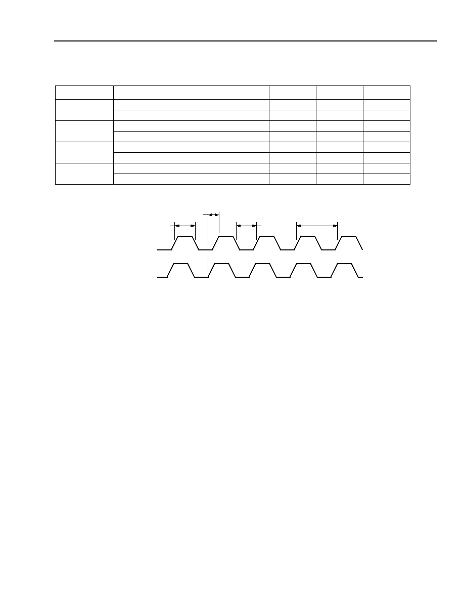
Lucent Technologies Inc.
33
Preliminary Data Sheet
LU3X31T-T64 Single-Port 3 V
July 2000
10/100 Ethernet Transceiver TX
Clock Timing
(continued)
Table 33. Transmit Clock (Input and Output)
* Specified at
±
100 ppm.
5-6785(F)
Figure 7. Transmit Timing (Input and Output)
Symbol
Description
Min
Max
Unit
t1
TXCLK High Pulse Width (100 Mbits/s)
14
26
ns
TXCLK High Pulse Width (10 Mbits/s)
140
260
ns
t2
X
IN
Rise to TXCLK Rise (100 Mbits/s)
14
--
ns
X
IN
Rise to TXCLK Rise (10 Mbits/s)
28
--
ns
t3
TXCLK Low Pulse Width (100 Mbits/s)
14
26
ns
TXCLK Low Pulse Width (10 Mbits/s)
140
260
ns
t4
TXCLK Period (100 Mbits/s)*
40
40
ns
TXCLK Period (10 Mbits/s)*
400
400
ns
X
IN
t2
t3
t1
t4
TXCLK
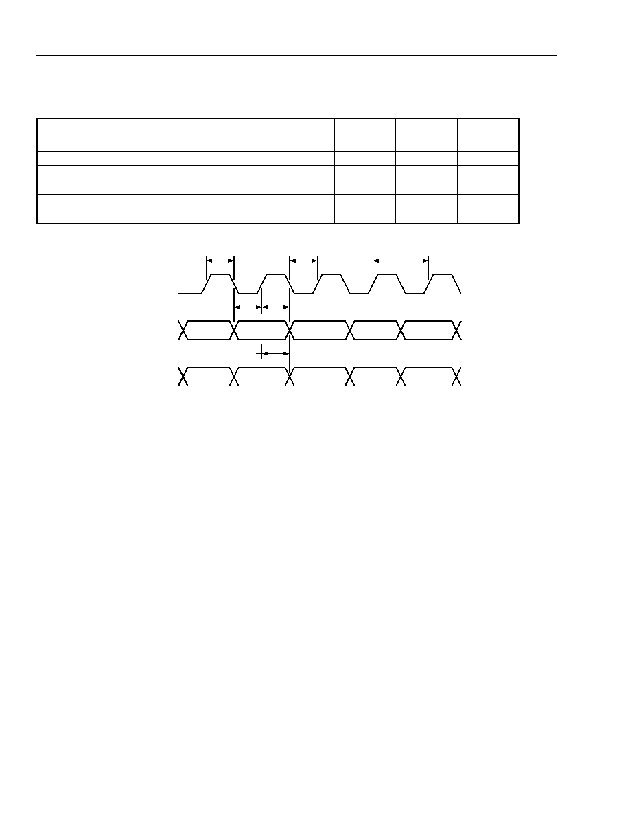
LU3X31T-T64 Single-Port 3 V
Preliminary Data Sheet
10/100 Ethernet Transceiver TX
July 2000
34
Lucent Technologies Inc.
Clock Timing
(continued)
Table 34. Management Clock
5-6786(F)
Figure 8. Management Timing
Symbol
Description
Min
Max
Unit
t1
MDC High Pulse Width
200
--
ns
t2
MDC Low Pulse Width
200
--
ns
t3
MDC Period
400
--
ns
t4
MDIO(I) Setup to MDC Rising Edge
10
--
ns
t5
MDIO(O) Hold Time from MDC Rising Edge
10
--
ns
t6
MDIO(O) Valid from MDC Rising Edge
0
300
ns
MDC
t2
t1
MDIO(I)
MDIO(O)
t4
t5
t6
t3
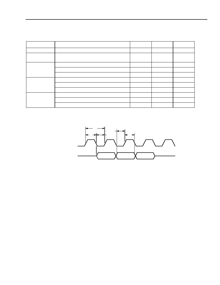
Lucent Technologies Inc.
35
Preliminary Data Sheet
LU3X31T-T64 Single-Port 3 V
July 2000
10/100 Ethernet Transceiver TX
Clock Timing
(continued)
Table 35. MII Receive Timing
5-6787(F).c
Figure 9. MII Receive Timing
Symbol
Description
Min
Max
Unit
t1
RXER, RXDV, RXD[3:0] Setup to RXCLK Rise
10
--
ns
t2
RXER, RXDV, RXD[3:0] Hold After RXCLK
Rise
10
--
ns
t3
RXCLK High Pulse Width (100 Mbits/s)
14
26
ns
RXCLK High Pulse Width (10 Mbits/s MII)
140
260
ns
RXCLK High Pulse Width (10 Mbits/s serial)
35
65
ns
t4
RXCLK Low Pulse Width (100 Mbits/s)
14
26
ns
RXCLK Low Pulse Width (10 Mbits/s MII)
140
260
ns
RXCLK Low Pulse Width (10 Mbits/s serial)
35
65
ns
t5
RXCLK Period (100 Mbits/s)
40
40
ns
RXCLK Period (10 Mbits/s MII)
400
400
ns
RXCLK Period (10 Mbits/s serial)
100
100
ns
RXCLK
t1
RXER, RXDV,
RXD[3:0]
t4
t5
t3
t2
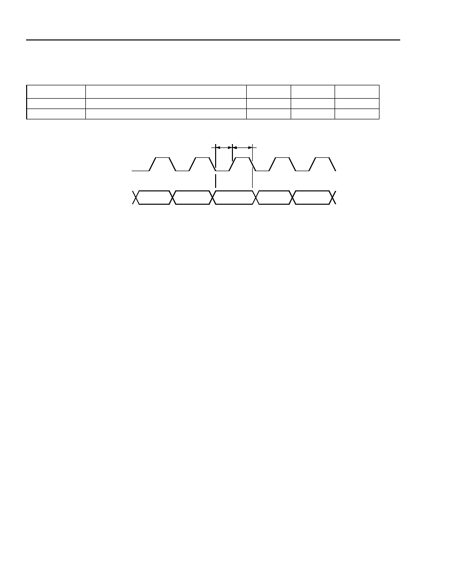
LU3X31T-T64 Single-Port 3 V
Preliminary Data Sheet
10/100 Ethernet Transceiver TX
July 2000
36
Lucent Technologies Inc.
Clock Timing
(continued)
Table 36. MII Transmit Timing
5-6788(F)
Figure 10. MII Transmit Timing
Symbol
Description
Min
Max
Unit
t1
TXER, TXEN, TXD[3:0] Setup to TXCLK Rise
10
--
ns
t2
TXER, TXEN, TXD[3:0] Hold After TXCLK Rise
0
25
ns
t2
t1
TXCLK
TXER, TXEN,
TXD[3:0]
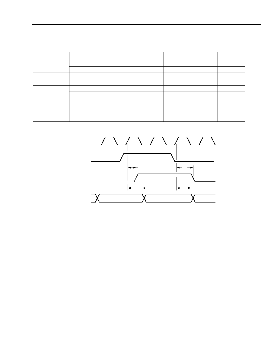
Lucent Technologies Inc.
37
Preliminary Data Sheet
LU3X31T-T64 Single-Port 3 V
July 2000
10/100 Ethernet Transceiver TX
Clock Timing
(continued)
Table 37. Transmit Timing
5-6789(F)
Figure 11. Transmit Timing
Symbol
Description
Min
Max
Unit
t1
TXEN Sampled to CRS High (100 Mbits/s)
0
4
bits
TXEN Sampled to CRS High (10 Mbits/s)
--
1.5
bits
t2
TXEN Sampled to CRS Low (100 Mbits/s)
0
16
bits
TXEN Sampled to CRS Low (10 Mbits/s)
--
16
bits
t3
Transmit Latency (100 Mbits/s)
6
14
bits
Transmit Latency (10 Mbits/s)
4
--
bits
t4
Sampled TXEN Inactive to End of Frame
(100 Mbits/s)
--
17
bits
Sampled TXEN Inactive to End of Frame
(10 Mbits/s)
--
5
bits
TXCLK
t1
CRS
TXEN
TPTX
PREAMBLE
t3
t2
t4
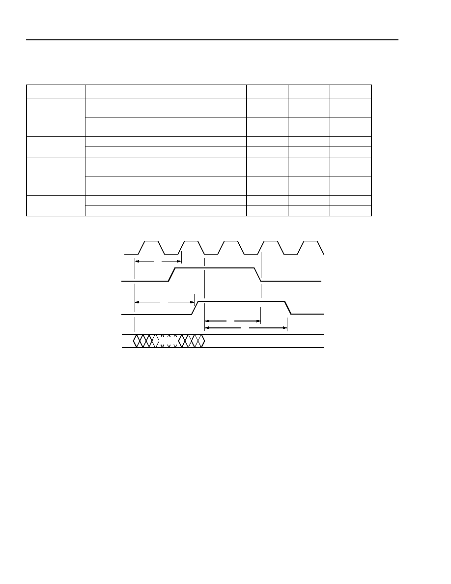
LU3X31T-T64 Single-Port 3 V
Preliminary Data Sheet
10/100 Ethernet Transceiver TX
July 2000
38
Lucent Technologies Inc.
Clock Timing
(continued)
Table 38. Receive Timing
5-6790(F)
Figure 12. Receive Timing
Symbol
Description
Min
Max
Unit
t1
Receive Frame to Sampled Edge of RXDV
(100 Mbits/s)
--
15
bits
Receive Frame to Sampled Edge of RXDV
(10 Mbits/s)
--
22
bits
t2
Receive Frame to CRS High (100 Mbits/s)
--
13
bits
Receive Frame to CRS High (10 Mbits/s)
--
5
bits
t3
End of Receive Frame to Sampled Edge of
RXDV (100 Mbits/s)
--
12
bits
End Receive Frame to Sampled Edge of RXDV
(10 Mbits/s)
--
4
bits
t4
End of Receive Frame to CRS Low (100 Mbits/s)
13
24
bits
End of Receive Frame to CRS Low (10 Mbits/s)
--
4.5
bits
RXCLK
CRS
RXDV
TPRX
t1
t2
t3
t4
DATA
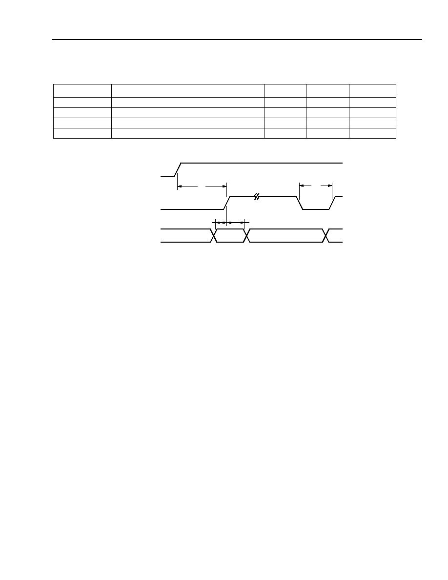
Lucent Technologies Inc.
39
Preliminary Data Sheet
LU3X31T-T64 Single-Port 3 V
July 2000
10/100 Ethernet Transceiver TX
Clock Timing
(continued)
Table 39. Reset and Configuration Timing
5-6791(F)
Figure 13. Reset and Configuration Timing
Symbol
Description
Min
Max
Unit
t1
Power On to Reset High
1.0
--
ms
t2
Reset Pulse Width
1.0
--
ms
t3
Configuration Pin Setup
1.0
--
ms
t4
Configuration Pin Hold
1.0
--
ms
V
CC
RSTZ
CONFIG
t3
t4
t2
t1

LU3X31T-T64 Single-Port 3 V
Preliminary Data Sheet
10/100 Ethernet Transceiver TX
July 2000
40
Lucent Technologies Inc.
Clock Timing
(continued)
Table 40. PMD Characteristics
5-6792(F).a
Figure 14. PMD Timing
Symbol
Description
Min
Max
Unit
t1
TPTX+/TPTX≠ Rise Time
3.0
5.0
ns
t2
TPTX+/TPTX≠ Fall Time
3.0
5.0
ns
t3
TP Skew
0
500
ps
t3
t2
t1
TPTX+
TPTX≠
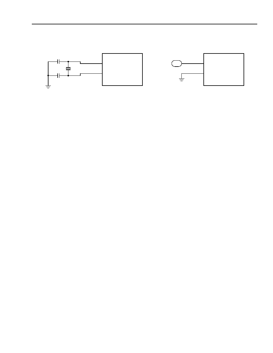
Lucent Technologies Inc.
41
Preliminary Data Sheet
LU3X31T-T64 Single-Port 3 V
July 2000
10/100 Ethernet Transceiver TX
Clock Timing
(continued)
5-6793(F).Cr.1
Figure 15. Connection Diagrams (Frequency References)
X
IN
X
OUT
25 MH
Z
±
50 PPM
20 pF
20 pF
X
IN
X
OUT
GND
25 MH
Z
OSC
±
50 PPM
25 MH
Z
CRYSTAL REFERENCE
25 MH
Z
OSCILLATOR REFERENCE
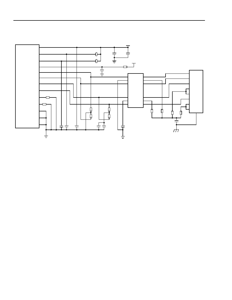
LU3X31T-T64 Single-Port 3 V
Preliminary Data Sheet
10/100 Ethernet Transceiver TX
July 2000
42
Lucent Technologies Inc.
Clock Timing
(continued)
5-6794(F).c
Figure 16. Connection Diagrams (10/100BTX Operation)
DIGITAL V
DD
TRANSMIT V
DD
RECEIVE V
DD
TPTX+
TPTX≠
TPRX+
TPRX≠
REF100
REF10
RECEIVE GND
TRANSMIT GND
DIGITAL GND
LU3X31T-T64
TRANSMIT
RECEIVE
MAGNETIC
RJ45
TX+
TX≠
RX+
UNUSED
UNUSED
RX≠
UNUSED
UNUSED
GND
301
4.64 k
0.1
µ
F
FB
FB
GND
V
CC
0.1
µ
F
22
µ
F
GND
0.1
µ
F
0.1
µ
F
50
50
54
54
CHASSIS GND
470 pF 3 kV
75
75
75
75
0.1
µ
F
1000 pF
CSVCC
4.7
µ
F
1
GND
V
CC
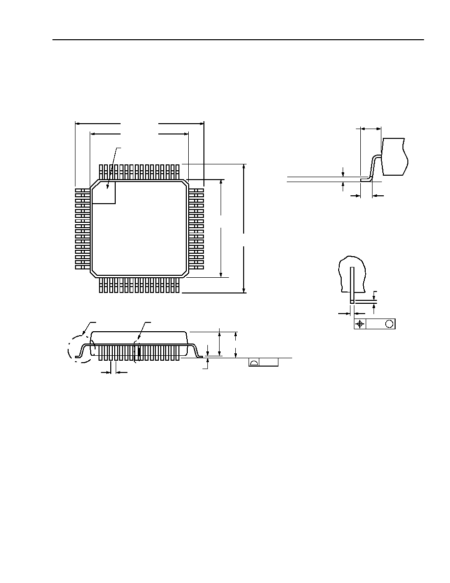
Lucent Technologies Inc.
43
Preliminary Data Sheet
LU3X31T-T64 Single-Port 3 V
July 2000
10/100 Ethernet Transceiver TX
Outline Diagram
64-Pin TQFP
Dimensions are in millimeters.
5-7101(F)
DETAIL A
0.50 TYP
1.60 MAX
SEATING PLANE
0.08
DETAIL B
0.05/0.15
1.40
±
0.05
10.00
±
0.20
12.00
±
0.20
1
64
49
16
17
32
48
33
10.00
±
0.20
12.00
±
0.20
PIN #1
IDENTIFIER ZONE
DETAIL A
0.45/0.75
GAGE PLANE
SEATING PLANE
1.00 REF
0.25
DETAIL B
0.19/0.27
0.08
M
0.106/0.200

Lucent Technologies Inc. reserves the right to make changes to the product(s) or information contained herein without notice. No liability is assumed as a result of their use or application. No
rights under any patent accompany the sale of any such product(s) or information.
Copyright © 2000 Lucent Technologies Inc.
All Rights Reserved
July 2000
DS00-358LAN (Replaces DS99-346LAN)
For additional information, contact your Microelectronics Group Account Manager or the following:
INTERNET:
http://www.lucent.com/micro
E-MAIL:
docmaster@micro.lucent.com
N. AMERICA:
Microelectronics Group, Lucent Technologies Inc., 555 Union Boulevard, Room 30L-15P-BA, Allentown, PA 18109-3286
1-800-372-2447, FAX 610-712-4106 (In CANADA: 1-800-553-2448, FAX 610-712-4106)
ASIA PACIFIC: Microelectronics Group, Lucent Technologies Singapore Pte. Ltd., 77 Science Park Drive, #03-18 Cintech III, Singapore 118256
Tel. (65) 778 8833, FAX (65) 777 7495
CHINA:
Microelectronics Group, Lucent Technologies (China) Co., Ltd., A-F2, 23/F, Zao Fong Universe Building, 1800 Zhong Shan Xi Road, Shanghai
200233 P. R. China Tel. (86) 21 6440 0468, ext. 325, FAX (86) 21 6440 0652
JAPAN:
Microelectronics Group, Lucent Technologies Japan Ltd., 7-18, Higashi-Gotanda 2-chome, Shinagawa-ku, Tokyo 141, Japan
Tel. (81) 3 5421 1600, FAX (81) 3 5421 1700
EUROPE:
Data Requests: MICROELECTRONICS GROUP DATALINE: Tel. (44) 7000 582 368, FAX (44) 1189 328 148
Technical Inquiries: GERMANY: (49) 89 95086 0 (Munich), UNITED KINGDOM: (44) 1344 865 900 (Ascot),
FRANCE: (33) 1 40 83 68 00 (Paris), SWEDEN: (46) 8 594 607 00 (Stockholm), FINLAND: (358) 9 4354 2800 (Helsinki),
ITALY: (39) 02 6608131 (Milan), SPAIN: (34) 1 807 1441 (Madrid)
LU3X31T-T64 Single-Port 3 V
Preliminary Data Sheet
10/100 Ethernet Transceiver TX
July 2000
Ordering Information
Device Code
Package
Temperature
Comcode
LU3X31T-T64
64-Pin TQFP
0
∞
C to 70
∞
C
108497249