 | –≠–ª–µ–∫—Ç—Ä–æ–Ω–Ω—ã–π –∫–æ–º–ø–æ–Ω–µ–Ω—Ç: LU5X34F | –°–∫–∞—á–∞—Ç—å:  PDF PDF  ZIP ZIP |

Preliminary Data Sheet
July 2000
LU5X34F
Quad Gigabit Ethernet Transceiver
Overview
The LU5X34F is a low-cost, low-power quad trans-
ceiver. It is used for data transmission over fiber or
coaxial media in conformance with
IEEE
* 802.3z
Gigabit Ethernet specification and Fibre Channel
ANSI
X3T11 at 1.0 Gbits/s and
1.25 Gbits/s.
Each of the four transceivers independently provides
complete serialize/deserialize (SERDES) and trans-
mit and receive functions. The device is available in a
217-pin PBGA package.
The transmitter section accepts TTL compatible data
at the 10-bit parallel input port. The parallel input
data is latched on the rising edge of TXCLKx. It also
accepts the low-speed, TTL compatible system
clock, REFCLK, and uses this clock to synthesize the
internal high-speed serial bit clock. The serialized
data is then available at the differential PECL out-
puts, terminated in 50
or 75
to drive either an
optical transmitter or coaxial media.
The receive section receives high-speed serial data
at its differential PECL input port. This data is fed to
the digital clock recovery section, which generates a
recovered clock and retimes the data. The retimed
data is deserialized and presented as 10-bit parallel
data on the output port. A divided-down version of
the recovered clock, synchronous with parallel data
bytes, is also available as a TTL compatible output.
The receive section recognizes the comma character
and aligns the comma-containing byte on the word
boundary, when ENCDET = 1.
Features
s
Designed to operate in Ethernet, fibre channel,
Firewire
, or backplane applications.
s
Operationally compliant to
IEEE
802.3z Gigabit
Ethernet specification.
s
Operationally compliant to Fibre Channel
ANSI
X3T11. Provides FC-0 services at 1.0 Gbits/s--
1.25 Gbits/s (10-bit encoded data rate).
s
100 MHz--125 MHz differential or single-ended
reference clock.
s
10-bit parallel, TTL-compatible I/O interface.
s
8-bit/10-bit encoded data.
s
High-speed comma character recognition (K28.1,
K28.5, K28.7) for latency-sensitive applications
and alignment to word boundary.
s
Two 50 MHz--62.5 MHz receive-byte clocks.
s
Single analog PLL design requires no external
components for the frequency synthesizer.
s
Novel digital data lock in receiver avoids the need
for multiple analog PLLs.
s
Expandable beyond four serializer/deserializers.
s
PECL high-speed interface I/O for use with optical
transceiver or coaxial copper media.
s
Requires one external resistor for PECL output ref-
erence-level definition.
s
Low-power digital CMOS technology.
s
Less than 2 W total power dissipation per quad
transceiver.
s
3.3 V ± 5% power supply.
s
0 ∞C--70 ∞C ambient temperature.
s
Stand-alone transceiver product.
s
Transceiver macrocell template.
s
Available in 217-pin PBGA package.
*
IEEE
is a registered trademark of The Institute of Electrical and
Electronics Engineers, Inc.
ANSI
is a registered trademark of American National Standards
Institute.
FireWire
is a registered trademark of Apple Computer, Inc.

2
Table of Contents
Lucent Technologies Inc.
Contents
Page
Table
Page
LU5X34F
Preliminary Data Sheet
Quad Gigabit Ethernet Transceiver
July 2000
Overview ....................................................................1
Features.....................................................................1
Functional Description ...............................................3
Transmitter Section .................................................3
Receiver Section .....................................................3
Lock to Reference ...................................................3
Byte Alignment ........................................................4
Parallel Output Port.................................................4
Loopback Mode Operation......................................4
Powerup Sequence.................................................5
Device Reset...........................................................5
Sleep Mode .............................................................5
Block Diagrams .......................................................6
Block Diagrams (continued) ....................................7
Input/Output Information ............................................8
Electrical Specifications ...........................................14
Transmitter ............................................................14
Receiver ................................................................14
Receiver (continued) .............................................15
Timing Characteristics .............................................16
Serial Timing .........................................................16
Receiver Section Timing .......................................17
Receiver Port Timing.............................................17
Transmitter Section Timing ...................................18
Application Section ..................................................19
Test Modes ..............................................................22
Outline Diagram .......................................................24
217-pin PBGA .......................................................24
Ordering Information ................................................25
Table 1. Receive Circuit Operating Modes ............. 3
Table 2. Definition of Bit Transmission/Reception
Order .................................................................... 4
Table 3a. Pinout--Channel A I/O............................ 9
Table 3b. Pinout--Channel B I/O.......................... 10
Table 3c. Pinout--Channel C I/O.......................... 11
Table 3d. Pinout--Channel D I/O ......................... 12
Table 3e. Pinout--Common I/O ............................ 13
Table 3f. Pinout--Power I/O ................................. 13
Table 4. Reference Clock Specifications
(REFCLK and REFCLKN) .................................. 14
Table 5. PLL Specifications .................................. 14
Table 6. Output Jitter at 1.0 Gbit/s--1.25 Gbits/s
Data Rate ........................................................... 14
Table 7. Input Data Rate ....................................... 14
Table 8. Data Lock Characteristics ....................... 14
Table 9. Power Dissipation ................................... 15
Table 10. dc Electrical Specifications ................... 15
Table 11. Absolute Maximum Ratings .................. 15
Table 12. Serial Output Timing Levels .................. 16
Table 13. Serial Input Interface Timing ................ 16
Table 14. Receiver Parallel Port Timing ............... 17
Table 15. Transmitter Timing at Parallel Interface 18
Table 16. External Resistor Value vs. Differential
Output Level Viewing ......................................... 20
Table 17. External Resistor Value vs. Differential
Output Level Viewing ......................................... 21
Table 18. Test Modes ........................................... 22
Figure
Page
Figure 1. LU5X34F Quad Gigabit Ethernet Transceiver
Block Diagram ........................................................ 6
Figure 2. LU5X34F Single-Channel Transceiver Func-
tional Diagram ........................................................ 7
Figure 3. Pin Designations (Top View) ..................... 8
Figure 4. Serial Interface Timing ............................. 16
Figure 5. Receiver Section Timing .......................... 17
Figure 6. Receiver Port Timing ............................... 17
Figure 7. Parallel Interface Transmit Timing ........... 18
Figure 8. Reference Clock Connections with Single-
Ended and Differential Sources............................ 19
Figure 9. Typical Termination for a Single-Channel,
High-Speed Serial Transmit-and-Receive Port in a
50
Backplane Application ................................. 20
Figure 10. Typical Termination for a Single-Channel,
High-Speed Serial Transmit Port Interfacing a 5 V
GBIC Transceiver ................................................. 21

3
Lucent Technologies Inc.
Preliminary Data Sheet
LU5X34F
July 2000
Quad Gigabit Ethernet Transceiver
Functional Description
The LU5X34F transceiver provides for data transmis-
sion over fiber or coaxial media at 1.0 Gbits/s to
1.25 Gbits/s. The block diagram of the quad transceiver
is shown in Figure 1 and the four-channel application
pinout for the 217-pin PBGA package is given in
Figure 3 and Table 3.
Transmitter Section
The transmitter accepts 8b/10b encoded bits in 10-bit
parallel form and converts to serial format for up to
1.25 Gbits/s transmission. The serial nonreturn to zero
(NRZ) bits are then shifted out of the device at a maxi-
mum rate of 1.25 Gbits/s. Internally, the device uses
two parallel shift registers that operate at half rate (i.e.,
a maximum of 625 MHz) for reduced power consump-
tion. The two shift registers drive the PECL output
buffer in an interleaved manner to construct the
1.25 Gbits/s output data stream.
The typical transmit-and-receive, high-speed I/O inter-
facing for a single-channel backplane application is
shown in Figure 9.
The transmit shift register and other circuits are driven
with clocks generated from a 500 MHz--625 MHz inter-
nal clock. This internal clock is sourced from a voltage-
controlled oscillator (VCO) that is locked to the external
reference of 100 MHz--125 MHz. The internal transmit
phase- lock loop multiplies the frequency of the input
reference clock by a factor of 5, and controls the trans-
mit jitter bandwidth with appropriate design of the jitter
transfer function. The transmit phase-lock loop gener-
ates multiple clock phases that are all used by each of
the four receiver circuits. The clock phases are derived
from the transmit VCO.
Receiver Section
Each of the quad receiver circuits recovers clock from
and retimes the serial input data. The data is input to
the receiver on differential PECL buffers. External ter-
mination resistors are supplied by the user in accor-
dance with
ANSI
standard, X3T11. The serial
differential inputs, HDINP and HDINN, are ac-coupled
to the device and internally biased to the PECL input
common-mode range center. See Figure 9 for the typi-
cal application and termination of the transmission
lines.
The receiver data-retiming circuit uses a digital timing
recovery loop that compares the phase of the input
data to multiple phases of the on-device VCO in the
transmit section. One of the phases is chosen to retime
the receive data. A digital low-pass filter is used in the
timing recovery loop to reject jitter from the data input.
A novel phase interpolation circuit permits the retiming
clock's phase to be stepped with fine resolution for pre-
cise alignment of the sampling clock within the data
eye. Use of this digital data locking scheme for each
receiver advantageously avoids the use of multiple
analog phase-lock loops on-device that can potentially
injection lock to one another. Additionally, the digital
data locking loop maintains precise loop dynamics,
hence, the jitter transfer function is process and tem-
perature independent.
Lock to Reference
The receive circuit has two modes of operation: lock to
reference, and lock to data with retiming. When no data
or invalid data is present on the HDINP and HDINN
input pins, the user can program the device to ignore
the input data by setting LCKREFN equal to logic 0. In
this mode, neither the PECL input buffer nor the RX
parallel data bus toggles. In normal operation, the
LCKREFN is a logic 1 and the receiver attempts to lock
to the incoming data. If the input data is invalid or out-
side the nominal ± frequency range, the receive digital
PLL will simply ramp the phase of the output clock until
it locks to data.
Table 1. Receive Circuit Operating Modes*
* REFCLK requirements are given in Table 4, and receive PLL specifications are given in Table 5.
Mode
Lock to Reference
Lock to Receive Data
LCKREFN = 1 (normal operation)
Not applicable.
Continually attempts to lock to
data.
LCKREFN = 0
Lock to clock, output data does not
toggle. Disable PECL input buffer.
Not applicable.

4
4
Lucent Technologies Inc.
LU5X34F
Preliminary Data Sheet
Quad Gigabit Ethernet Transceiver
July 2000
Functional Description
(continued)
Byte Alignment
When ENCDET = 1, the LU5X34F recognizes the
comma character and aligns this 10-bit character to the
word boundary, bits RX[0:9].
COMDET =1 when the parallel output word contains a
byte-aligned comma character. The COMDET flag will
continue to pulse a logic 1 whenever a byte-aligned
comma character is at the parallel output port, indepen-
dent of ENCDET. When ENCDET = 0, there are two
possible scenarios depending upon when the comma
character is received.
1. If byte alignment had been previously achieved when
ENCDET had been a logic 1, the COMDET flag will
continue to pulse a logic 1 whenever a byte-aligned
comma character is at the parallel output port. If a
comma character occurs that is not on the word
boundary, no attempt will be made to align this
comma character and the COMDET flag will remain
at a logic 0.
2. If byte alignment had not been previously achieved
when ENCDET had been a logic 1, then the first
(and only the first) comma character received will be
aligned to the word boundary. COMDET will pulse
when the comma character is aligned to the word
boundary.
Parallel Output Port
Timing for the parallel output data and the 50 MHz to
62.5 MHz receive-byte clock is given in Table 14.
Two low data rate receive-byte clocks are available as
TTL compatible outputs during use of the parallel out-
put port in 10-bit mode. RXCLK1 is the receive byte
clock used by the protocol device to register bytes 0
and 2. RXCLK0 is the receive-byte clock used by the
protocol device to register bytes 1 and 3, and it is
180 degrees out of phase with RXCLK1. Both RXCLK1
and RXCLK0 can be stretched during byte alignment
but not truncated or slivered. The maximum allowable
frequency of these two clocks under all circumstances,
excluding start-up, will not exceed 80 MHz. The start-
up time is specified as 1 ms.
Loopback Mode Operation
A control signal input, EWRAP, selects between two
possible sets of inputs: normal data (HDINP, HDINN) or
internal loopback data. When EWRAP = 1, the serial
output ports, HDOUTP and HDOUTN, remain active.
The serial transmit data prior to the PECL output driver
is directed to the data recovery circuit, where clock is
recovered and data is resynchronized to the recovered
clock. Retimed data and clock then go to the serial-to-
parallel converter.
Table 2. Definition of Bit Transmission/Reception Order*
* Lower case
X
signifies channel A, B, C, or D.
Serial Transmit/
Receive Rate
TX
X
[9:0]
RX
X
[9:0]
1.0 Gbits/s to 1.25 Gbits/s TX
X
[0] bit serially transmitted first at
HDOUT
X
P, HDOUT
X
N
RX
X
[0] bit received first at serial inputs
HDIN
X
P, HDIN
X
N

5
Lucent Technologies Inc.
Preliminary Data Sheet
LU5X34F
July 2000
Quad Gigabit Ethernet Transceiver
Functional Description
(continued)
Powerup Sequence
The power ramp time for the LU5X34F is specified at
V
DD
> 2.7 V within 20 µs of start-up. Once 2.7 V is
reached, the device is held in reset for 15 µs--70 µs.
The REFCLK must be active and within specification at
this point and remain active while the device is pow-
ered up, unless in Reset.
When signals RESET, BYPPLL, and LPWR are all low,
the following start-up sequence occurs:
1. 0 µs--32 µs, the analog PLL is held at minimum fre-
quency to allow dc bias to settle.
2. 32 µs--262 µs, the analog PLL has locked-in and
receiver analog circuits start to lock-in.
3. 262 µs--326 µs, the receiver analog circuits are
locked; receiver starts to lock onto incoming data.
4. After 358 µs, the receiver is locked onto incoming
data and can be viewed at the parallel output ports.
The comma-detect circuit is enabled at this point,
allowing byte alignment if ENCDET = 1.
If LCKREFN goes low after the 358 µs, the receiver will
sit idle. When LCKREFN goes high, the receiver will be
locked onto data after 2 µs.
Device Reset
The RESETN input to the device is active-low. When
activated with a pulse duration of 1 µs, the RESETN sig-
nal globally resets the device and the following is per-
formed:
1. The single analog PLL is forced to operate at the mini-
mum frequency possible for its VCO. The PLL will not
be locked in this condition.
2. The HDOUTP, HDOUTN outputs are forced to a
PECL logic 0.
3. The deserializer clocks, but input data at HDINP,
HDINN is ignored and the RX[9:0] signals remain in
their previous state.
4. The phase interpolation/selection circuits are deacti-
vated and the selected phase is reset.
5. The receiver digital low-pass filter in the DPLL is reset.
Normally, a reset is not necessary for correct operation,
although a reset can aid rapid lock-in of the internal
PLL circuitry. This active-low pin is internally pulled
high.
Sleep Mode
The LU5X34F has a sleep mode that is activated by
enabling LPWR. In this mode, a divided-down version
of the REFCLK is used to refresh the dynamic circuits
within the transceiver. The PLL is powered down in this
mode also. LCKREFN can also be activated to reduce
the power even further. Note that complete powerdown
for I
DD
Q testing is not supported due to the dynamic
logic used in the high-speed sections of the trans-
ceiver. The lock-in sequence timing is needed when
coming out of sleep mode.
6
Lucent Technologies Inc.
LU5X34F
Preliminary Data Sheet
Quad Gigabit Ethernet Transceiver
July 2000
Functional Description
(continued)
Block Diagrams
* Synchronous with REFCLK(N).
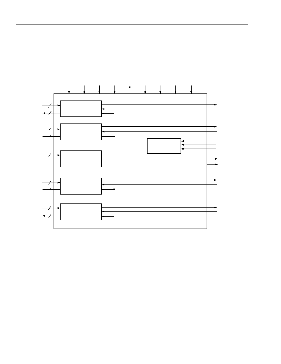
Figure 1. LU5X34F Quad Gigabit Ethernet Transceiver Block Diagram
LPWR
RESET
TXCLK
[A
:D]
*
E
NCDE
T
[
A:D]
COMDE
T[A
:D]
EWR
A
P[
A:
D
]
LC
KRE
F
N[A:D]
OLREF
OLRVS
RXA[9:0]
TXA[9:0]
RXB[9:0]
TXB[9:0]
TEST[5:1]
LDST[A:D]
BYPPLL
RXCLK0[A:D]
RXCLK1[A:D]
RXC[9:0]
TXC[9:0]
RXD[9:0]
TXD[9:0]
TEST CIRCUITS
TRANSCEIVER A
TRANSCEIVER B
ANALOG PLL
TRANSCEIVER C
TRANSCEIVER D
HDINDP
HDINDN
HDOUTDP
HDOUTDN
HDOUTCN
HDOUTCP
HDINCN
HDINCP
REFCLKN
REFCLK
HDOUTBN
HDOUTBP
HDINBN
HDINBP
HDOUTAN
HDOUTAP
HDINAN
HDINAP
2
2
2
2
2
2
2
2
2
5-8808(F)
7
Lucent Technologies Inc.
Preliminary Data Sheet
LU5X34F
July 2000
Quad Gigabit Ethernet Transceiver
Functional Description
(continued)
Block Diagrams
(continued)
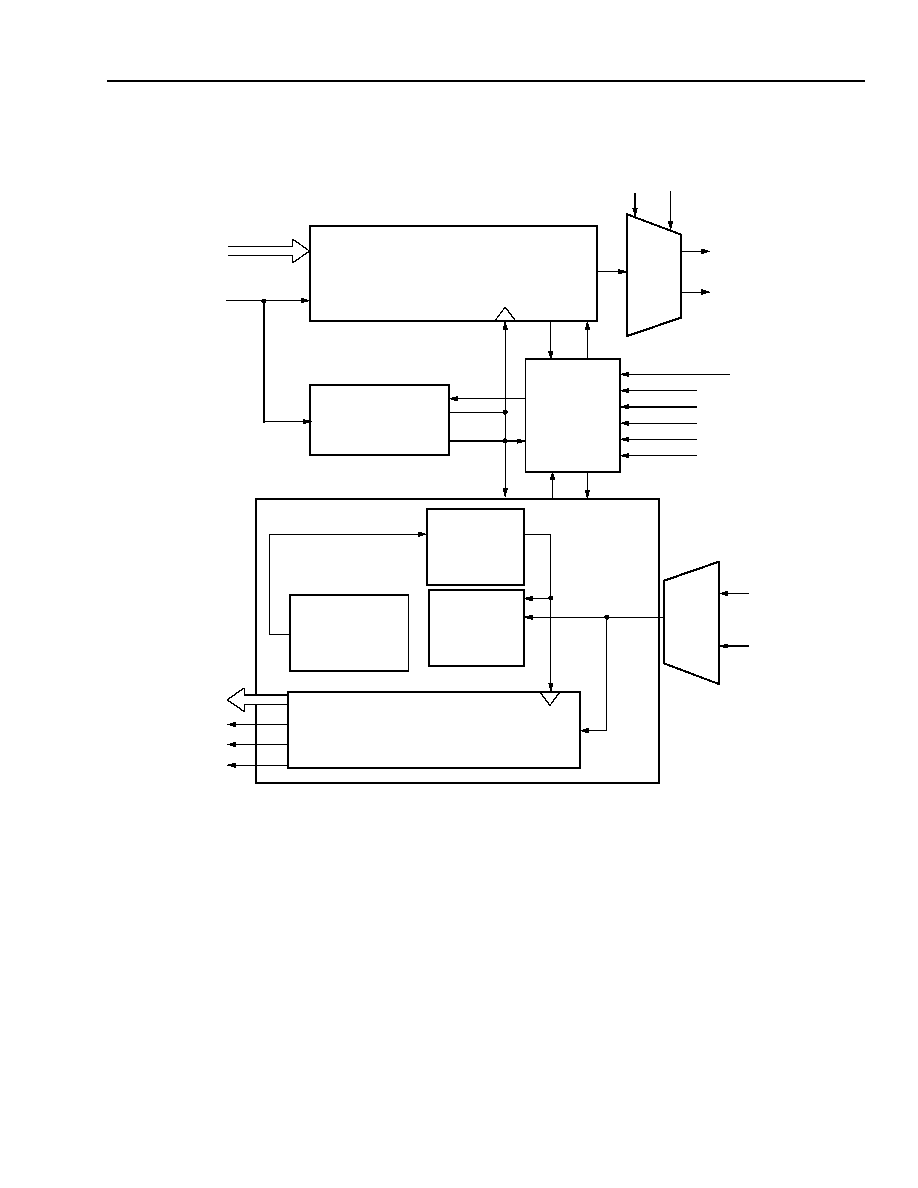
Figure 2. LU5X34F Single-Channel Transceiver Functional Diagram
DATA IN
LOAD
SERIALIZER
SERIAL DATA
OUT
PECL
HDOUTP
HDOUTN
TEST[5:1] / LDST
BYPPLL
RESETN
LPWR
ENCDET
HDINP
HDINN
PECL
GLOBAL
CONTROL
PHASE SELECT/
INTERPOLATION
DESERIALIZER
ANALOG PLL
TX[9:0]
REFCLK
RX[9:0]
RXCLK0
RXCLK1
DATA RETIMING, SERIAL-TO-PARALLEL
CONVERSION AND COMMA DETECTION
SERIAL
DATA
IN
LOW-PASS FILTER
DIGITAL
PHASE
DETECTOR
COMDET
EWRAP
OLREF OLRVS
5-8809(F).a
.
8
Lucent Technologies Inc.
LU5X34F
Preliminary Data Sheet
Quad Gigabit Ethernet Transceiver
July 2000
Input/Output Information
Figure 3. Pin Designations (Top View)
RXB8
2
RXB7
RXB6
RXB2
EWRAPA
TXB6
TXB8
N/C
VDD
TXB4
TXB5
TXB7
TXCLKB
TXB0
TXB1
TXB3
TXB2
RXA1
RXA0
N/C
VDD
RXA3
RXA4
RXA2
VSS
RXA5
RXA6
RXA8
VDD
RXA7
RXA9
RXCLK0A
N/C
COMDETA
RXCLK1A
TXCLKA
TXA7
N/C
VDD
TXA8
TXA4
VSS
RXB5
RXB1
RXCLK0B
RXB9
VSS
RXB4
TXB9
RXCLK1B
COMDETB
VSS
LCKREFA
LCKREFB
TEST2
TEST4
ENCDETA
EWRAPB
RESETN
TEST3
N/C
LDSTA
ENCDETB
TEST1
RXB3
RXB0
LDSTB
VDD
BYPPLL
REFCLK
ENCDETC
ENCDETD
TEST5
REFCLKN
LDSTC
LDSTD
LPWR
EWRAPC
LPBKD
N/C
VSS
VDD
LCKREFC
TXC2
LCKREFD
TXC1
TXC5
TXC5
TXC0
TXC4
TXC8
VSS
TXC3
TXC7
VSS
N/C
TXC6
VSS
RXCLK1C
COMDETC
RXCLK0C
RXC8
RXC6
RXC4
RXC9
RXC5
RXC3
RXC0
RXC1
RXC2
N/C
TXD1
VDD
TXD0
TXD2
TXD3
VSS
TXD6
TXD4
TXD5
VDD
TXD10
TXD8
TXD7
N/C
RXCLK1D
TXCLKD
N/C
RXD6
RXD9
N/C
RXCLK0D
RXD2
RXD5
RXD8
COMDETD
VSS
RXD1
RXD4
RXD7
HDOUTDN
VSS
RXD0
RXD3
HDINDN
HDOUTDP
VSS
N/C
VDDR
VSSRC
N/C
VDDTD
VSSRC
VDDTC
HDOUTCP
HDINDP
OLREF
HDINCP
HDOUTCN
VDDTC
OLRVS
N/C
HDINCN
N/C
HDOUTAP
HDOUTBP
VDDR
VSST
HDINBP
HDOUTBN
VSSP
VREG
VSSRB
VDDTB
VDDP
N/C
VDDTB
VDDP
VSSP
N/C
TXA6
TXA3
VSST
HDINAN
TXA2
VSST
HDINAP
HDOUTAN
VSST
VSSRA
VDDTA
VSSRB
N/C
VSSRA
VDDTA
HDINBN
TXA9
TXA5
TXA1
TXA0
VSSRD
VSSRD
VDDTD
N/C
N/C
TXCLKC
N/C
RXC7
VSS
VSS
VSS
VSS
VSS
VSS
VSS
VSS
VSS
A
U
T
R
P
N
M
L
K
J
H
G
F
E
D
C
B
1
3
4
5
6
7
8
9
10
11
12
13
14
15
16
17
5-8880(F)

9
Lucent Technologies Inc.
Preliminary Data Sheet
LU5X34F
July 2000
Quad Gigabit Ethernet Transceiver
Input/Output Information
(continued)
Table 3a. Pinout--Channel A I/O
Name
Pin
I/O
Level
Description
TXA9
TXA8
TXA7
TXA6
TXA5
TXA4
TXA3
TXA2
TXA1
TXA0
A14
C13
D12
B14
A15
D13
C14
B15
A16
A17
Input
TTL/
CMOS
Channel A, Transmit Data [9:0].
Parallel input bits [9:0], one 10-bit, 8b/10b encoded
data byte, clocked-in on the rising edge of TXCLKA.
TXA0 is the LSB.
RXA9
RXA8
RXA7
RXA6
RXA5
RXA4
RXA3
RXA2
RXA1
RXA0
B11
C10
A11
B10
A10
B9
A9
C9
A8
B8
Output
TTL/
CMOS
Channel A, Receive Data [9:0].
Parallel output bits [9:0], one 10-bit data type, clocked-
out on the alternate rising edge of RXCLK0A,
RXCLK1A. RXA0 is the LSB.
TXCLKA
C12
Input
TTL/
CMOS
Transmit Clock (100 MHz--125 MHz).
Used to latch TXA[9:0] data into the LU5X34F.
Synchronous with REFCLK(N)
RXCLK0A
C11
Output
TTL/
CMOS
Channel A, Receive Byte-Align Clock 0.
RXCLK1A
B12
Output
TTL/
CMOS
Channel A, Receive Byte-Align Clock 1.
ENCDETA
E2
Input
TTL/
CMOS
Channel A, Enable Comma Detect A.
COMDETA
A12
Output
TTL/
CMOS
Channel A, Byte-Aligned Comma A.
EWRAPA
D1
Input
TTL/
CMOS
Channel A, Loopback at Serial I/O A.
LCKREFNA
E1
Input
TTL/
CMOS
Channel A, Lock Receiver to Clock.
HDINAP,
HDINAN
D15, E14
Input
PECL
Channel A, Differential Serial Inputs.
HDOUTAP,
HDOUTAN
F14, E15
Output
PECL
Channel A, Differential Serial Outputs.
LDSTA
F3
Input
TTL/
CMOS
Channel A, Load Test[5:1] Inputs.

10
Lucent Technologies Inc.
LU5X34F
Preliminary Data Sheet
Quad Gigabit Ethernet Transceiver
July 2000
Input/Output Information
(continued)
Table 3b. Pinout--Channel B I/O
Name
Pin
I/O
Level
Description
TXB9
TXB8
TXB7
TXB6
TXB5
TXB4
TXB3
TXB2
TXB1
TXB0
A4
B5
C6
A5
B6
A6
C7
D7
B7
A7
Input
TTL/
CMOS
Channel B, Transmit Data [9:0].
Parallel input bits [9:0], one 10-bit, 8b/10b encoded
data byte, clocked-in on the rising edge of TXCLKB.
TXB0 is the LSB.
RXB9
RXB8
RXB7
RXB6
RXB5
RXB4
RXB3
RXB2
RXB1
RXB0
B3
A2
A1
B1
C2
D3
E4
C1
D2
F4
Output
TTL/
CMOS
Channel B, Receive Data [9:0].
Parallel output bits [9:0], one 10-bit data type, clocked-
out on the alternate rising edge of RXCLK0B,
RXCLK1B. RXB0 is the LSB.
TXCLKB
D6
Input
TTL/
CMOS
Transmit Clock (100 MHz--125 MHz).
Used to latch TXB[9:0] data into the LU5X34F.
Synchronous with REFCLK(N)
RXCLK0B
A3
Output
TTL/
CMOS
Channel B, Byte-Align Clock 0.
RXCLK1B
B4
Output
TTL/
CMOS
Channel B, Byte-Align Clock 1.
ENCDETB
G3
Input
TTL/
CMOS
Channel B, Enable Comma Detect.
COMDETB
C4
Output
TTL/
CMOS
Channel B, Byte-Aligned Comma.
EWRAPB
F2
Input
TTL/
CMOS
Channel B, Loopback at Serial I/O.
LCKREFNB
F1
Input
TTL/
CMOS
Channel B, Lock Receiver to Clock.
HDINBP,
HDINBN
F15, E17
Input
PECL
Channel B, Differential Serial Inputs.
HDOUTBP,
HDOUTBN
G14, G15
Output
PECL
Channel B, Differential Serial Outputs.
LDSTB
G4
Input
TTL/
CMOS
Channel B, Load TEST[5:1] inputs.

11
Lucent Technologies Inc.
Preliminary Data Sheet
LU5X34F
July 2000
Quad Gigabit Ethernet Transceiver
Input/Output Information
(continued)
Table 3c. Pinout--Channel C I/O
Name
Pin
I/O
Level
Description
TXC9
TXC8
TXC7
TXC6
TXC5
TXC4
TXC3
TXC2
TXC1
TXC0
T1
R2
P3
N4
R1
P2
N3
M4
P1
N2
Input
TTL/
CMOS
Channel C, Transmit Data [9:0].
Parallel input bits [9:0], one 10-bit, 8b/10b encoded
data byte, clocked in on the rising edge of TXCLKC.
TXC0 is the LSB.
RXC9
RXC8
RXC7
RXC6
RXC5
RXC4
RXC3
RXC2
RXC1
RXC0
P6
R5
U4
T5
R6
U5
T6
R7
P7
U6
Output
TTL/
CMOS
Channel C, Receive Data [9:0].
Parallel output bits [9:0], one 10-bit data type, clocked-
out on the alternate rising edge of RXCLK0C,
RXCLK1C. RXC0 is the LSB.
TXCLKC
U2
Input
TTL/
CMOS
Transmit Clock (100 MHz--125 MHz).
Used to latch TXC[9:0] data into the LU5X34F.
Synchronous with REFCLK(N)
RXCLK0C
P5
Output
TTL/
CMOS
Channel C, Byte-Align Clock 0.
RXCLK1C
R4
Output
TTL/
CMOS
Channel C, Byte-Align Clock 1.
ENCDETC
L1
Input
TTL/
CMOS
Channel C, Enable-Comma Detect.
COMDETC
T4
Output
TTL/
CMOS
Channel C, Byte-Aligned Comma.
EWRAPC
K3
Input
TTL/
CMOS
Channel C, Loopback at Serial I/O.
LCKREFNC
L4
Input
TTL/
CMOS
Channel C, Lock Receiver to Clock.
HDINCP,
HDINCN
L16, M17
Input
PECL
Channel C, Differential Serial Inputs.
HDOUTCP,
HDOUTCN
M15, M16
Output
PECL
Channel C, Differential Serial Outputs.
LDSTC
L2
Input
TTL/
CMOS
Channel C, Load Test[5:1] Inputs.

12
Lucent Technologies Inc.
LU5X34F
Preliminary Data Sheet
Quad Gigabit Ethernet Transceiver
July 2000
Input/Output Information
(continued)
Table 3d. Pinout--Channel D I/O
Name
Pin
I/O
Level
Description
TXD9
TXD8
TXD7
TXD6
TXD5
TXD4
TXD3
TXD2
TXD1
TXD0
R10
T10
U10
R10
U9
T9
U8
T8
U7
R8
Input
TTL/
CMOS
Channel D, Transmit Data [9:0].
Parallel input bits [9:0], one 10-bit, 8b/10b encoded
data byte, clocked-in on the rising edge of TXCLKD.
TXD0 is the LSB.
RXD9
RXD8
RXD7
RXD6
RXD5
RXD4
RXD3
RXD2
RXD1
RXD0
R12
T13
U14
P12
R13
T14
U15
P13
R14
T15
Output
TTL/
CMOS
Channel D, Receive Data [9:0].
Parallel output bits [9:0], one 10-bit data type, clocked-
out on the alternate rising edge of RXCLK0D,
RXCLK1D. RXD0 is the LSB.
TXCLKD
T11
Input
TTL/
CMOS
Transmit Clock (100 MHz--125 MHz).
Used to latch TXD[9:0] data into the LU5X34F.
Synchronous with REFCLK(N)
RXCLK0D
U12
Output
TTL/
CMOS
Channel D, Byte-Align Clock 0.
RXCLK1D
R11
Output
TTL/
CMOS
Channel D, Byte-Align Clock 1.
ENCDETD
M1
Input
TTL/
CMOS
Channel D, Enable Comma Detect.
COMDETD
U13
Output
TTL/
CMOS
Channel D, Byte-Aligned Comma.
EWRAPD
L3
Input
TTL/
CMOS
Channel D, Loopback at Serial I/O.
LCKREFND
N1
Input
TTL/
CMOS
Channel D, Lock Receiver to Clock.
HDINDP,
HDINDN
N15, P16
Input
PECL
Channel D, Differential Serial Inputs.
HDOUTDP,
HDOUTDN
R16, P15
Output
PECL
Channel D, Differential Serial Outputs.
LDSTD
M2
Input
TTL/
CMOS
Channel D, Load Test[5:1] Inputs.
13
Lucent Technologies Inc.
Preliminary Data Sheet
LU5X34F
July 2000
Quad Gigabit Ethernet Transceiver
Input/Output Information
(continued)
Table 3e. Pinout--Common I/O
* For related information, see Table 18, Test Modes.
Table 3f. Pinout--Power I/O
Name
Pin
I/O
Level
Description
OLREF
K16
Input/
Output
Analog
PECL Level Set Resistor Terminal 1.
OLRVS
K17
Input/
Output
Analog
PECL Level Set Resistor Terminal 2.
LPWR
J3
Input
TTL/
CMOS
Device Low-Power Mode.
RESETN
G2
Input
TTL/
CMOS
Device Reset (Active-Low).
TEST5*
J2
Input/
Output
TTL/
CMOS
Global Test Control Input/Output.
TEST4*
H1
Input
TTL/
CMOS
Local Test Control Input.
TEST3*
H2
Input
TTL/
CMOS
Local Test Control Input.
TEST2*
G1
Input
TTL/
CMOS
Local Test Control Input.
TEST1*
H3
Input
TTL/
CMOS
Local Test Control Input.
BYPPLL
J1
Input
TTL/
CMOS
Test Control, PLL Bypass Mode.
REFCLK,
REFCLKN
K1, K2
Input
PECL or
TTL/
CMOS
Reference Clock Input (100 MHz--125 MHz).
Used by the transmitter PLL to generate the
1.0 Gbits/s-- 1.25 Gbits/s serial data; has a +100 ppm
tolerance requirement.
Name
Pin
Description
V
DD
D5, D8, D10, B13, H4, K4, P8, P10
Device Digital Power.
V
DD
P
G17, H16
PLL Power.
V
DD
T
X
D16, D17, F17, G16, L15, N16, N14, T17,
High-Speed Analog Transmitter Power.
V
DD
R
H14, K14
High-Speed Analog Receiver Power.
V
SS
B2, C3, D4, D9, H8, H9, H10, J4, J8, J9, J10,
K8, K9, K10, P4, P9, P14, R3, R15, T2, T16
Device Digital Ground.
V
SS
P
H15, H17
PLL Ground.
V
SS
T
B16, C15, D14, J14
High-Speed Analog Transmitter Ground.
V
SS
R
X
C16, C17, E16, F16, K15, L14, P17, R17
High-Speed Analog Receiver Ground.
14
Lucent Technologies Inc.
LU5X34F
Preliminary Data Sheet
Quad Gigabit Ethernet Transceiver
July 2000
Electrical Specifications
Transmitter
Table 4. Reference Clock Specifications (REFCLK and REFCLKN)
* Measured at 50% amplitude point.
Table 5. PLL Specifications
Table 6. Output Jitter
at 1.0 Gbit/s--1.25 Gbits/s Data Rate
Receiver
Table 7. Input Data Rate
Table 8. Data Lock Characteristics
*
Data pattern: 101010 . . . .
Data pattern: 1111100000 . . . .
Parameter
Min
Max
Unit
Frequency Range
100
125
MHz
Frequency Tolerance
≠100
100
ppm
Duty Cycle*
40
60
%
Rise Time (PECL)
--
0.8
ns
Fall Time (PECL)
--
0.8
ns
Rise Time (TTL/CMOS)
--
1.5
ns
Fall Time (TTL/CMOS)
--
1.5
ns
In-band Jitter, 1 Gbit/s--1.25 Gbits/s
--
30
ps
p-p
Out-of-Band Jitter
--
50
ps
p-p
Parameter
Min
Typ
Max
Unit
Bandwidth
--
1.5 --
MHz
Jitter Peaking
--
0.5
--
dB
Lock Time
--
--
230
µs
Parameter
Min
Max
Unit
Deterministic --
0.08
UI
p-p
Random
--
0.12
UI
p-p
Total
--
0.2
UI
p-p
Parameter
Min
Max Unit
Frequency Range
1.0
1.25
Gbits/s
Frequency Tolerance with REFCLK
≠100
100
ppm
Parameter
Min
Typ
Max
Unit
Bandwidth*
0.3
--
1*
MHz
Jitter Peaking*
--
0.5
--
dB
Lock Time*
--
--
2
µs
15
Lucent Technologies Inc.
Preliminary Data Sheet
LU5X34F
July 2000
Quad Gigabit Ethernet Transceiver
Electrical Specifications
(continued)
Receiver
(continued)
Table 9. Power Dissipation *
* Depending on application (PCB layout), etc.
Table 10. dc Electrical Specifications*
* Depending on application (PCB layout), etc.
Table 11. Absolute Maximum Ratings
Parameter
Min
Typ
Max Unit
Power --
--
2.0
W
Package Thermal
Resistance
TBD
--
TBD
∞C/W
Sleep Mode (LPWR)
--
TBD
--
mW
Parameter
Symbol
Condition
Min
Typ
Max Unit
Supply Voltage
V
DD
, V
DD
P
--
3.135
3.3
3.465
V
Output Low
V
OL
--
0
--
0.6
V
Output High
V
OH
--
2.4
--
V
DD
V
Input Low
V
IL
--
0
--
0.8
V
Input High
V
IH
--
2.0
--
V
DD
V
Diff. PECL Output
Load, as in Figure 9.
800
--
--
mV
Diff. PECL Input
Source configuration,
as in Figure 9.
400
--
1600
mV
Parameter
Min Typ
Max Unit
Supply Voltage
3.135
3.3
3.465
V
TTL High Input Voltage
3.0
--
3.6
V
PECL Output Current
--
--
16
mA
Junction Operating Temperature
0
--
125
∞C
Storage Temperature
≠65
--
150
∞C
16
Lucent Technologies Inc.
LU5X34F
Preliminary Data Sheet
Quad Gigabit Ethernet Transceiver
July 2000
Timing Characteristics
Serial Timing
Table 12. Serial Output Timing Levels
Figure 4. Serial Interface Timing
Table 13. Serial Input Interface Timing
Description
Min
Typ
Max Unit
Rise Time 20%--80%
0.17
0.2
0.22
ns
Fall Time 80%--20%
0.17
0.2
0.22
ns
Common Mode
V
DD
/2 ≠ 0.1
V
DD
/2
V
DD
/2 + 0.1
V
Differential Swing
0.8
--
1.6
V
p-p
Load (See Table 16)
50
--
75
Description
Min
Max Unit
Rise Time (tR)
150
225
ps
Fall Time (tF)
150
225
ps
Differential Swing (V
DIFF
)
0.4
1.6
mV
p-p
Source Impedance
50
75
Data Eye Opening
320
--
ps
V
DIFF
D
WIN
tF/tR
5-8813(F)
17
Lucent Technologies Inc.
Preliminary Data Sheet
LU5X34F
July 2000
Quad Gigabit Ethernet Transceiver
Timing Characteristics
(continued)
Receiver Section Timing
Figure 5. Receiver Section Timing
Receiver Port Timing
Figure 6. Receiver Port Timing
Table 14. Receiver Parallel Port Timing
* 1.25 Gbits/s.
0.5 pF load.
Symbol
Parameter
Min
Max
Units
--
RXCLK[1:0] Frequency*
--
62.5
MHz
--
RXCLK[1:0] Low
7.0
9.0
ns
--
RXCLK[1:0] High
7.0
9.0
ns
tR/F
RXCLK[1:0] (0.4 V to 2.6 V)
0.2
0.5
ns
tR/F
Data Output (0.4 V to 2.6 V)
0.2
0.5
ns
tS
Setup Time
3.0
--
ns
tH
Hold Time
2.0
--
ns
tSKEW
Skew
--
1.0
ns
RX[9:0]
D7.2
HDNIP
RECOVERED CLOCK
RXCLK1
RXCLK0
COMDET
(INTERNAL)
K28.5
K28.5
D7.2
D0.0
D1.0
RXCLK1
RXCLK0
RX
RX0
RX1
RX2
RX3
RXCLK1 HIGH
RXCLK1 LOW
RXCLK PERIOD
tSKEW
tS
tH
tS
tH
5-8813 (F)
5-8814(F)

18
Lucent Technologies Inc.
LU5X34F
Preliminary Data Sheet
Quad Gigabit Ethernet Transceiver
July 2000
Timing Characteristics
(continued)
Transmitter Section Timing
* Synchronous with REFCLK(N).
Figure 7. Parallel Interface Transmit Timing
Table 15. Transmitter Timing at Parallel Interface
Description
Min
Max Unit
Conditions
Data Setup
2
--
ns
With positive edge TXCLK
Data Hold
2
--
ns
With positive edge TXCLK
Rise Time
--
1
ns
--
Fall Time
--
1
ns
--
SYNTHESIZED CLOCK
SERIALIZED DATA
TX[9:0]
TXCLK*
155
126
375
34A
155
126
375
5-8815(F)
19
Lucent Technologies Inc.
Preliminary Data Sheet
LU5X34F
July 2000
Quad Gigabit Ethernet Transceiver
Application Section
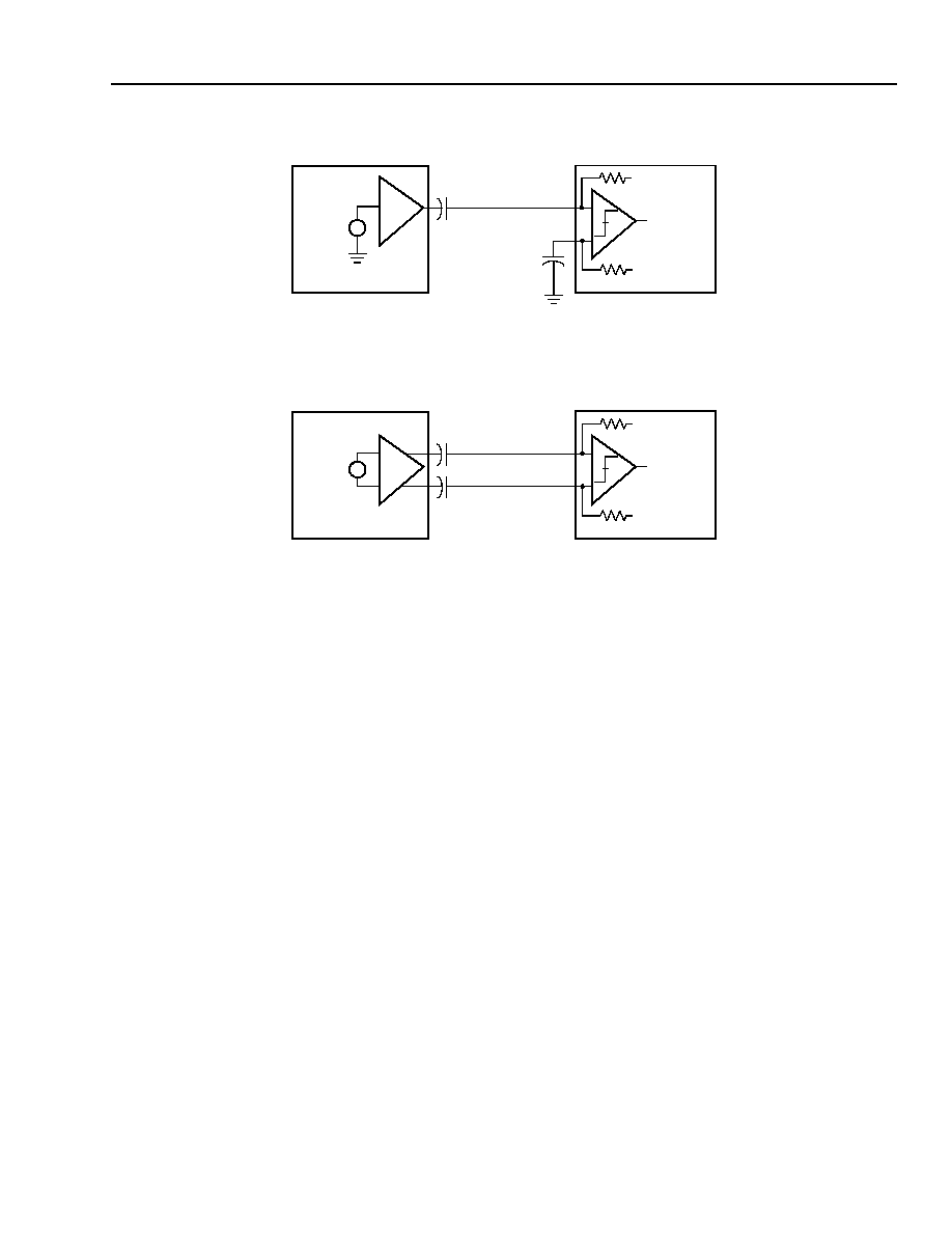
Figure 8. Reference Clock Connections with Single-Ended and Differential Sources
CLOCK
SOURCE
REFCLK
REFCLKN
BIAS
BIAS
INTERNAL
CLOCK
LU5X34F
CLOCK
SOURCE
REFCLK
REFCLKN
BIAS
BIAS
INTERNAL
CLOCK
LU5X34F
SINGLE-ENDED CLOCK SOURCE
DIFFERENTIAL CLOCK SOURCE
1.0 nF
5-8013(F)
20
Lucent Technologies Inc.
LU5X34F
Preliminary Data Sheet
Quad Gigabit Ethernet Transceiver
July 2000
Application Section
(continued)
* External resistor connected between OLREF and OLRVS
.
See Table 16 for external resistor value.
Damping resistor, maximum = 10
.
Figure 9. Typical Termination for a Single-Channel, High-Speed Serial
Transmit-and-Receive Port in a 50
Backplane Application
Table 16. External Resistor Value vs. Differential Output Level Viewing
Resistor Value (
)
Termination Impedance (
)
Differential Output Voltage (V)
7.5 k/11.25 k
50/75
0.8
5 k/7.5 k
1.2
4 k/6 k
1.6
5-8811(F).c
HDINP
HDINN
HDOUTP
HDOUTN
0.01
µ
F
10
50
50
100
0.01
µ
F
TRANSMIT
RXCLK
X
1
RXCLK
X
0
RX
X
[9:0]
OLREF
OLRVS
TX
X
[9:0]
TXCLK
10
0.1
µ
F
*
Z
O
= 50
Z
O
= 50
RECEIVE
LU5X34F
LU5X34F

21
Lucent Technologies Inc.
Preliminary Data Sheet
LU5X34F
July 2000
Quad Gigabit Ethernet Transceiver
Application Section
(continued)
* External resistor connected between OLREF and OLRVS
.
See Table 17 for resistor value vs. termination impedance and output swing.
Damping resistor, maximum = 10
.
Figure 10. Typical Termination for a Single-Channel, High-Speed Serial
Transmit Port Interfacing a 5 V GBIC Transceiver
Table 17. External Resistor Value vs. Differential Output Level Viewing
Resistor Value (
)
Termination Impedance (
)
Differential Output Voltage (V)
7.5 k/11.25 k
50/75
0.8
5 k/7.5 k
1.2
4 k/6 k
1.6
5-8811(F)b
TX(+)
TX(≠)
HDOUTP
HDOUTN
0.01
µ
F
10
50
50
191
0.01
µ
F
TRANSMIT
LU5X34F
TRANSMIT
GBIC
OLREF
OLRVS
TXA[9:0]
REFCLK
10
0.1
µ
F
*
Z
O
= 50
68
191
Z
O
= 50
68
5 V

22
Lucent Technologies Inc.
LU5X34F
Preliminary Data Sheet
Quad Gigabit Ethernet Transceiver
July 2000
Test Modes
Note: Test modes are intended for manufacture test only and are not guaranteed to be operational. They may be
modified or eliminated without prior notice.
The device has per-channel test modes as well as global test modes. The bypass PLL, BYPPLL, is a global test
input because it modifies the operation of the analog PLL. Test bits TEST[4:1] generally operate in the localized
mode. The LDST[A:D] inputs are enable signals that permit the TEST[4:1] signals to be injected into a particular
channel.
For example, if LDSTA = 1, the TEST[4:1] signals directly control the test modes in the A channel. Once
LDSTA = 0, the previous values of TEST[4:1] are held for the A channel. The TEST[4:1] signals control the four
channels (A, B, C, D) via level sense latches that are gated with the LDST[A:D] inputs. TEST[5] is a global test pin
used for both injection of signals as well as for monitoring points within the device.
Table 18. Test Modes
Global
Local Test Configuration
Global
Operation
BYPPLL
TEST1
TEST2
TEST3
TEST4
TEST5
0
1
1
1
1
X
Normal operation.
0
1
1
1
0
Output
Analog PLL feedback signal viewed at
TEST5 pin.
0
1
1
0
1
X
Transceiver operates normally except
RX[9:0] output is from digital filter, not
the serial data.
0
1
1
0
0
Output
Transceiver operates normally except
RX[9:0] output is from digital filter and
the analog PLL feedback signal is
viewed at TEST5 pin.
0
1
0
1
P
P
Digital filter forced to count. Pulses
applied at TEST4 increment accumula-
tor; pulses at TEST5 decrement accu-
mulator.
0
1
0
0
P
P
RX[9:0] output is from digital filter, not
the serial data. Digital filter forced to
count. Pulses applied at TEST4 incre-
ment accumulator; pulses at TEST5
decrement accumulator.
0
0
1
1
1
X
Parallel loopback. TX[9:0] = RX[9:0].
RX[9:0] remains active.
0
0
1
1
0
Output
Parallel loopback. TX[9:0] = RX[9:0]
and analog PLL feedback signal viewed
at TEST5 pin. RX[9:0] remains active.
0
0
1
0
1
X
RX[9:0] output is from digital filter, not
the serial data. Receive channel is held
in reset. BYPPLL overrides this reset.
0
0
1
0
0
Output
RX[9:0] output is from digital filter, not
the serial data. Receive channel is held
in reset. BYPPLL overrides this reset.
Analog PLL feedback signal viewed at
TEST5 pin

23
Lucent Technologies Inc.
Preliminary Data Sheet
LU5X34F
July 2000
Quad Gigabit Ethernet Transceiver
Test Modes
(continued)
Table 18. Test Modes (continued)
Global
Local Test Configuration
Global
OPERATION
BYPPLL
TEST1
TEST2
TEST3
TEST4
TEST5
0
0
0
1
0
Output
Transmitter is held in reset. BYPPLL
overrides this reset. Analog PLL feed-
back signal viewed at TEST5 pin.
0
0
0
0
1
X
Transmitter and receiver are held in
reset. RX[9:0] output is from digital fil-
ter, not the serial data.
0
0
0
0
0
Output
Transmitter and receiver are held in
reset. RX[9:0] output is from digital fil-
ter, not the serial data. Analog PLL
feedback signal viewed at TEST5 pin.
1
X
X
1
C-0
C-90
Analog PLL is bypassed for low speed
functional test. A low-speed clock is
input to TEST4, and a quadrature clock
is applied to TEST5. Frequency of
clocks is 5X REFCLK, but here REF-
CLK is lowered to about 1 MHz.
1
X
X
0
C-0
C-90
Analog PLL is bypassed for low-speed
functional test. A low-speed clock is
input to TEST4, and a quadrature clock
is applied to TEST5. Frequency of
clocks is 5X REFCLK, but here REF-
CLK is lowered to about 1 MHz.
RX[9:0] output is from digital filter, not
the serial data.
24
Lucent Technologies Inc.
LU5X34F
Preliminary Data Sheet
Quad Gigabit Ethernet Transceiver
July 2000
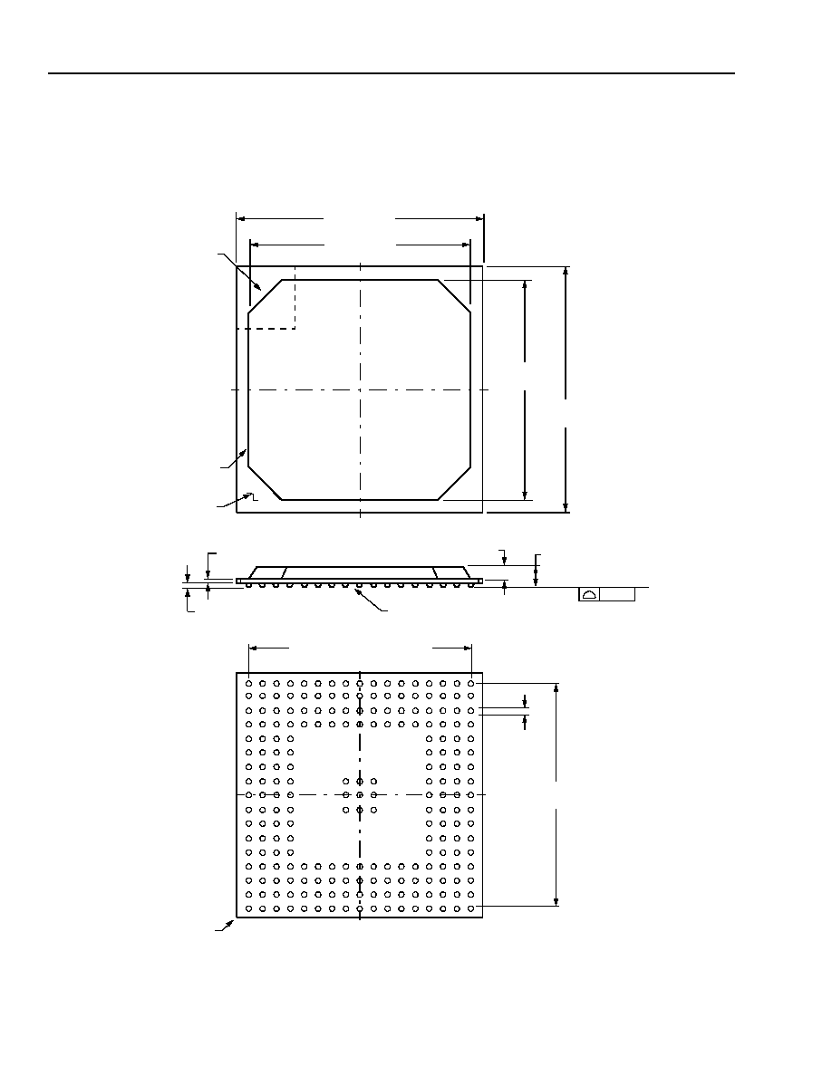
Outline Diagram
217-pin PBGA
Dimensions are in millimeters.
5-6562 (F)
0.36 ± 0.04
1.17 ± 0.05
2.13 ± 0.19
SEATING PLANE
SOLDER BALL
0.60 ± 0.10
0.20
A
B
C
D
E
F
G
H
J
K
L
M
N
P
R
T
U
1 2
3 4 5 6 7
8 9 10 11 12 13 14 15 16 17
16 SPACES @ 1.27 = 20.32
A1 BALL
CORNER
16 SPACES
@ 1.27 = 20.32
0.75 ± 0.15
PWB
MOLD
COMPOUND
23.00 ± 0.20
23.00
± 0.20
19.50
+0.70
≠0.00
19.50
+0.70
≠0.00
A1 BALL
IDENTIFIER ZONE

25
Lucent Technologies Inc.
Preliminary Data Sheet
LU5X34F
July 2000
Quad Gigabit Ethernet Transceiver
Ordering Information
Device Code
Comcode
Package
Temperature
LU5X34F
108497850
217-pin PBGA
0 ∞C--70 ∞C

For additional information, contact your Microelectronics Group Account Manager or the following:
INTERNET:
http://www.lucent.com/micro
E-MAIL:
docmaster@micro.lucent.com
N. AMERICA:
Microelectronics Group, Lucent Technologies Inc., 555 Union Boulevard, Room 30L-15P-BA, Allentown, PA 18109-3286
1-800-372-2447, FAX 610-712-4106 (In CANADA: 1-800-553-2448, FAX 610-712-4106)
ASIA PACIFIC: Microelectronics Group, Lucent Technologies Singapore Pte. Ltd., 77 Science Park Drive, #03-18 Cintech III, Singapore 118256
Tel. (65) 778 8833, FAX (65) 777 7495
CHINA:
Microelectronics Group, Lucent Technologies (China) Co., Ltd., A-F2, 23/F, Zao Fong Universe Building, 1800 Zhong Shan Xi Road, Shanghai
200233 P. R. China Tel. (86) 21 6440 0468, ext. 325, FAX (86) 21 6440 0652
JAPAN:
Microelectronics Group, Lucent Technologies Japan Ltd., 7-18, Higashi-Gotanda 2-chome, Shinagawa-ku, Tokyo 141, Japan
Tel. (81) 3 5421 1600, FAX (81) 3 5421 1700
EUROPE:
Data Requests: MICROELECTRONICS GROUP DATALINE: Tel. (44) 7000 582 368, FAX (44) 1189 328 148
Technical Inquiries: GERMANY: (49) 89 95086 0 (Munich), UNITED KINGDOM: (44) 1344 865 900 (Ascot),
FRANCE: (33) 1 40 83 68 00 (Paris), SWEDEN: (46) 8 594 607 00 (Stockholm), FINLAND: (358) 9 4354 2800 (Helsinki),
ITALY: (39) 02 6608131 (Milan), SPAIN: (34) 1 807 1441 (Madrid)
Lucent Technologies Inc. reserves the right to make changes to the product(s) or information contained herein without notice. No liability is assumed as a result of their use or application. No
rights under any patent accompany the sale of any such product(s) or information.
Copyright © 2000 Lucent Technologies Inc.
All Rights Reserved
July 2000
DS00-351LAN (Replaces DS00-007LAN)
LU5X34F
Preliminary Data Sheet
Quad Gigabit Ethernet Transceiver
July 2000