 | –≠–ª–µ–∫—Ç—Ä–æ–Ω–Ω—ã–π –∫–æ–º–ø–æ–Ω–µ–Ω—Ç: LUC4AS01 | –°–∫–∞—á–∞—Ç—å:  PDF PDF  ZIP ZIP |
Advance Product Brief
March 1997
LUC4AS01
ATM Switch Element (ASX)
Section 5.4
LUCENT TECHNOLOGIES--PROPRIETARY
Use pursuant to Company Instructions
Introduction
The ASX IC is part of the ATLANTA chip set consist-
ing of four devices that provide a highly integrated,
innovative, and complete VLSI solution for imple-
menting the ATM layer core of an ATM switch system.
The chip set enables construction of high-perfor-
mance, feature-rich, and cost-effective ATM switches,
scalable over a wide range of switching capacities.
This document discusses the ASX device.
Features
s
Functions as a highly efficient, 5 Gbits/s, shared
memory, ATM switching element for scalable
switch fabrics up to 25 Gbits/s.
-- In stand-alone mode, used as an 8 x 8 switch
fabric with 622 Mbits/s I/O rates.
-- Can be used as a building block for larger N x N
fabrics of up to 40 x 40 ports with 622 Mbits/s
I/O rate (25 Gbits/s total ATM throughput).
-- In three-stage mode, supports variable expan-
sion factors (4:8, 5:8, and 6:8) for more compact
fabric design with higher port density.
s
Works with other ATLANTA devices to provide total
system solutions for ATM switching.
-- Directly interfaces with the LUC4AB01 ATM
Buffer Manager (ABM) chip to support port card
buffering.
-- Directly interfaces with the LUC4AC01 ATM
Crossbar Element (ACE) chip for constructing
larger nonblocking, lossless, and self-routing
switch fabrics, organized into a three-stage
topology.
s
Incorporates a novel internal backpressure algo-
rithm based on separate on-chip queues for all fab-
ric ports to enable large scale cell buffers on the
port cards (up to 32K cells per port) using cost-
effective commonly available SRAMs.
s
Has an internal 512 cell memory, fully shared
across all queues, supplemented by the port card
buffers.
s
Supports four delay priorities per queue and uses
a programmable, weighted, round-robin scheduler
for servicing delay priorities.
s
Provides efficient unrestricted multicasting with
single copy storage.
s
Incorporates independent clocking of input ports to
facilitate robust distributed systems designs by
allowing for independent port card clocks or arbi-
trary clock skew introduced across backplanes
from separate port cards.
s
Uses differential clocking to provide noise immu-
nity. Parity and cell insertion/extraction aid in
detecting and tracking system errors.
s
Provides system diagnostic features, including
detection and reporting of the following error condi-
tions:
-- Input port parity error.
-- Input port overrun error.
-- Loss of input port clock.
-- CRC error on outgoing cell.
-- Linked list fault indication.
-- Test cell extraction.
s
Provides several performance/traffic indicators.
s
Supports a generic
Intel
* or
Motorola
compatible
16-bit microprocessor interface with interrupt.
s
Facilitates circuit board testing with on-chip
IEEE
standard boundary-scan.
s
Fabricated as a low-power monolithic IC in 0.5
µ
m,
3.3 V CMOS technology, with 5 V tolerant and TTL-
level compatible I/O.
s
Available in a 388-pin PBGA package.
*
Intel
is a registered trademark of Intel Corporation.
Motorola
is a registered trademark of Motorola, Inc.
IEEE
is a registered trademark of The Institute of Electrical and
Electronics Engineers, Inc.
2
2
Lucent Technologies Inc.
Advance Product Brief
March 1997
ATM Switch Element (ASX)
LUC4AS01
Section 5.4
LUCENT TECHNOLOGIES--PROPRIETARY
Use pursuant to Company Instructions
Description
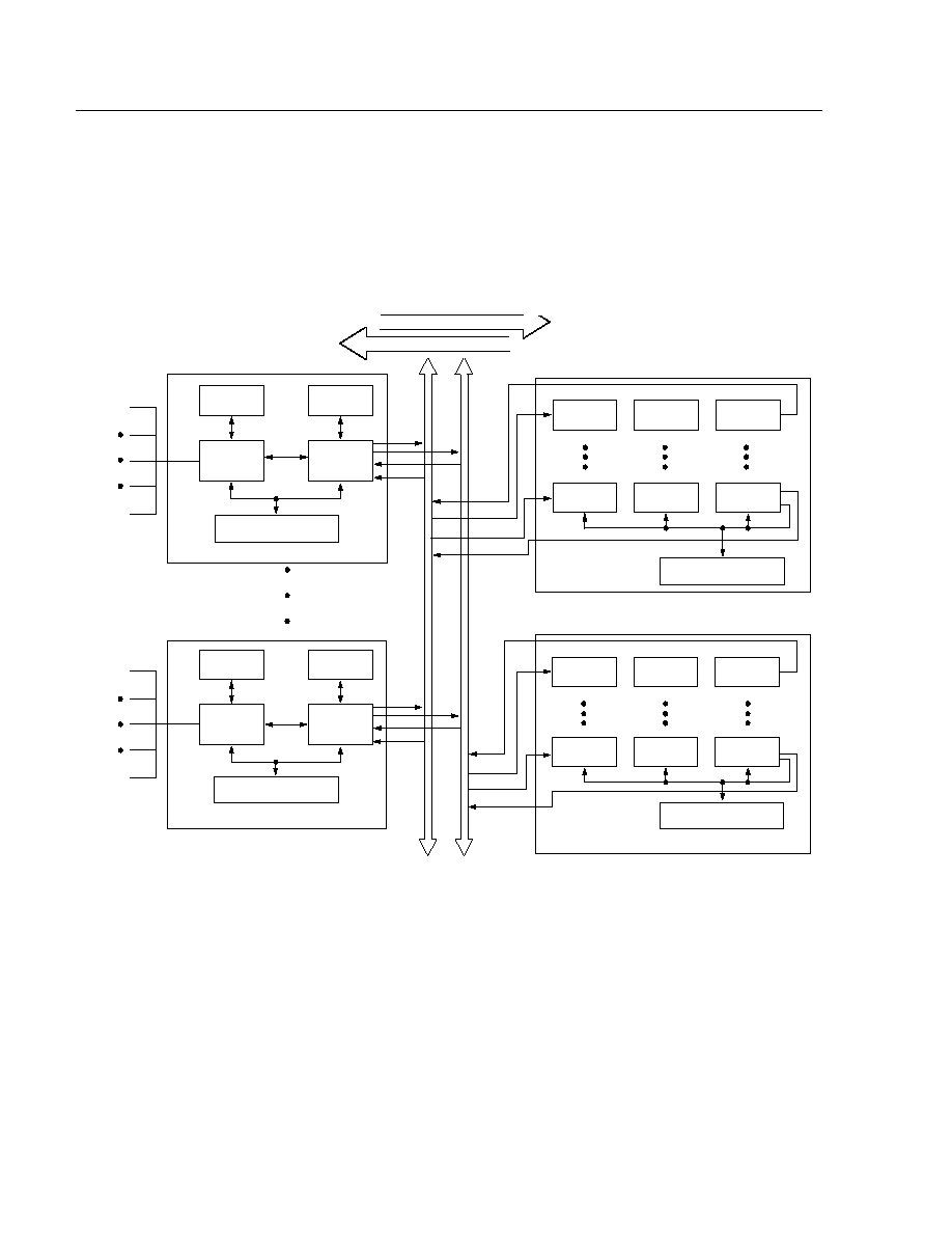
Figure 1 shows the architecture of an ATM switch
designed with the ATLANTA chip set. This document
summarizes ATLANTA switch fabrics and the
LUC4AS01 ATM Switch Element (ASX). The ATLANTA
ASX device provides the switching function for an ATM
switch fabric. This 8 x 8 switch element functions as a
complete 5 Gbits/s switch fabric with OC-12 equivalent
port rates, or as a building block for larger three stage
switch fabrics (up to 40 x 40 OC-12 equivalent ports,
25 Gbits/s systems). The ASX interfaces directly to
both the ATLANTA LUC4AC01 ATM Crossbar Element
(ACE) device (for linking switch elements) and the
LUC4AB01 ATM Buffer Manager (ABM) device (for
buffer management). High-performance, nonblocking,
lossless, and self-routing switch fabrics can be con-
structed using the ATLANTA chip set.
5-4554r9
Figure 1. Architecture of an ATM Switch Using the ATLANTA Chip Set
ALM
LUC4AU01
MICROPROCESSOR
INTERFACE
SRAM
LINE CARD #1
#1
#1
LINE CARD #N
N x N SWITCH FABRIC
#N
BA
CKPLANE
REDUND
ANT BA
CKPLANE
ABM
LUC4AB01
SRAM
PHYSICAL LAYER
INTERFACE (MPHY)
ALM
LUC4AU01
SRAM
ABM
LUC4B01
SRAM
ASX
LUC4AS01
ACE
LUC4AC01
ASX
LUC4AS01
ASX
LUC4AS01
ACE
LUC4AC01
ASX
LUC4AS01
#1
#1
#N
N x N REDUNDANT SWITCH FABRIC
#N
ASX
LUC4AS01
ACE
LUC4AC01
ASX
LUC4AS01
ASX
LUC4AS01
ACE
LUC4AC01
ASX
LUC4AS01
#1
#1
#N
INGRESS DIRECTION
EGRESS DIRECTION
#1
#1
#N
#N
#N
#N
1
M
PHY PORTS
1
M
PHY PORTS
MICROPROCESSOR
INTERFACE
MICROPROCESSOR
INTERFACE
MICROPROCESSOR
INTERFACE

Lucent Technologies Inc.
3
Advance Product Brief
March 1997
ATM Switch Element (ASX)
LUC4AS01
Section 5.4
LUCENT TECHNOLOGIES--PROPRIETARY
Use pursuant to Company Instructions
Description
(continued)
The ASX has an internal 512 cell memory, fully shared
across all queues; no external SRAM is required in the
fabric. It supports four delay priorities per queue and
uses a programmable weighted round-robin algorithm
for scheduling delay priority service. Novel techniques
are incorporated for congestion management. An inno-
vative Bell Labs-developed adaptive dynamic threshold
algorithm permits efficient buffer sharing while prevent-
ing any queue from seizing a disproportionate share of
the cell buffer. A novel internal backpressure algorithm
is applied to prevent the fabric cell buffer from overflow-
ing and increase buffer sharing of large-scale buffers
on the port cards using cost-effective, commonly avail-
able SRAMs. The ASX provides efficient unrestricted
multicasting with single copy storage.
The ASX also provides system diagnostic features.
Diagnostic reports include parity errors on inputs, inter-
nal memory overrun errors, and loss of input port
clock. In addition, a CRC is calculated on data input to
the ASX, passed through the ASX, then calculated
after the data is switched to ensure that silicon errors
have not been introduced. When a CRC error is
detected, a parity error is indicated in the data as it is
output from the ASX. Test cell extraction through the
microprocessor interface also aids in testability.
The ASX block diagram and a brief description of the
functionality follows.
5-4515aR9
Figure 2. ASX Block Diagram
INPUT
CLOCKING
26
12
12
12
12
12
12
8 (DATA)
1 (PARITY)
1 (START OF CELL)
2 (CLOCK)
BUFFER MEMORY
QUEUE
TEST ACCESS
OUTPUT
12
12
12
12
12
12
12
12
3
5
8 (DATA)
1 (PARITY)
1 (START OF CELL)
2 (CLOCK)
TEST ACCESS
PORT
PROCESSOR
INPUT
PROCESSOR
INPUT
PROCESSOR
INPUT
PROCESSOR
INPUT
PROCESSOR
INPUT
PROCESSOR
INPUT
PROCESSOR
INPUT
PROCESSOR
12
12
PROCESSOR
ARBITER
PROCESSOR
OUTPUT
PROCESSOR
OUTPUT
PROCESSOR
OUTPUT
PROCESSOR
OUTPUT
PROCESSOR
OUTPUT
PROCESSOR
OUTPUT
PROCESSOR
OUTPUT
PROCESSOR
EGRESS
PORTS
INGRESS
PORTS
SYNCHRONIZATION
GTSYNC
SYSTEM CLOCK
MICROPROCESSOR
INTERFACE
RESET (GRST)
OUTPUT ENABLE
(ASXOE)
AND
(BMEM)
(QP)
(ARB)
CONFIGURATION AND
STATUS REGISTERS
(GCLK)
FIRST/THIRD STAGE
BACKPRESSURE
(F1T3_1, F1T3_E,
F1T3CLK)
TO ACE
(CB1_m, CB2_n)
SOURCE
8
FEEDBACK
GENERATION CIRCUIT
AND CELL
EXTRACTION FIFO
(MPI)
PORT (JTAG)
4
4
Lucent Technologies Inc.
Advance Product Brief
March 1997
ATM Switch Element (ASX)
LUC4AS01
Section 5.4
LUCENT TECHNOLOGIES--PROPRIETARY
Use pursuant to Company Instructions
Description
(continued)
Overview
As shown in Figure 2, data for each port is clocked into
an input processor, passed to internal cell buffers, and
then routed to the appropriate output processor. The
queue processor, routing and arbitration circuit, and
backpressure feedback generation circuit controls the
movement of data into and out of the cell buffer mem-
ory. Control and status is communicated through a
16-bit asynchronous microprocessor interface.
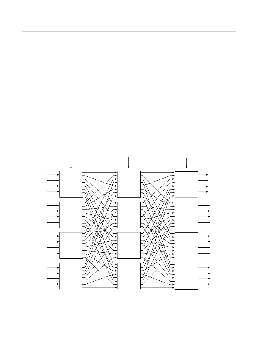
Figure 3 shows an example 16 x 16 ATLANTA-based
switch fabric. The switch fabric will switch any of the
16 inputs to any of the 16 outputs. This is achieved by
staging devices and is referred to as a three-stage
switch fabric. The input stage is called the
first stage
(expander), and the output stage is called the
third
stage
(concentrator). The center stage consists of the
companion ACE device. The ACE is functionally similar
to the ASX, but without the internal cell buffer (a hand-
shake protocol between the ASX and the ACE ensures
that the ACE need not store data). Conceptually, the
first-stage ASX expands the number of paths available
for switching the data, while the third stage concen-
trates data from the center stage. The ASX device sup-
ports 4:8, 5:8, and 6:8 expansion modes. The
expansion mode is configurable, depending on cost
and performance objectives, as well as the type of traf-
fic expected.
A three-stage ASX/ACE based switch fabric can sup-
port up to 40 ports with 622 Mbits/s I/O rates. A 40-port
(25 Gbits/s total ATM throughput) fabric design would
use eight devices per stage in a 5:8 expansion mode.
5-4523R5
Figure 3. Example 16 x 16 @ 622 Mbits/s Switch Fabric (10 Gbits/s throughput)
ASX
MODULE #0
ASX
MODULE #1
ASX
MODULE #2
ASX
MODULE #3
ACE
MODULE #0
ACE
MODULE #1
ACE
MODULE #2
ASX
MODULE #0
ASX
MODULE #1
ASX
MODULE #2
ASX
MODULE #3
INPUT FROM
PORT CARDS
OUTPUT TO
PORT CARDS
FIRST-STAGE EXPANDER
THIRD-STAGE CONCENTRATOR
CENTER-STAGE CROSSBAR
ACE
MODULE #3

Lucent Technologies Inc.
5
Advance Product Brief
March 1997
ATM Switch Element (ASX)
LUC4AS01
Section 5.4
LUCENT TECHNOLOGIES--PROPRIETARY
Use pursuant to Company Instructions
Description
(continued)
Input Processors
The input processors are responsible for accepting
data onto the device. There are eight input processors,
one for each port. Any of the inputs can be used
regardless of the expansion factor. Each input port has
eight data bits, one parity bit, one start of cell bit, and a
differential clock. The microprocessor must enable the
appropriate input ports. The input processor does pre-
liminary processing and stores the header, payload,
and the internally generated CRC-8 of the arriving cell
until it can be written to the internal cell buffer. Input
ports are clocked independently from 10 MHz to
100 MHz. This independent clocking facilitates back-
plane based system designs with distributed port
cards.
The input port interface is designed to minimize the risk
of undetected errors. The differential clock provides
system noise immunity to prevent errors. In addition,
the input processor detects the presence of an input
clock and reports when the input clock is lost. The input
processor also checks for incoming parity errors. And,
an internal CRC-8 is generated for each ATM cell that
is transferred to the internal cell buffer for switching.
The CRC is then checked before the switched data is
transferred off the device. Furthermore, the input pro-
cessor also detects and reports input port overrun
errors.
Buffer Memory
The ASX contains 512 cells of internal memory. This
memory is shared among all active system ports (up to
40). The buffer memory stores the local header, the
ATM header, and the cell payload until this data can be
shifted out to the appropriate output port.
Output Processors
The output processors perform many of the same func-
tions as the input processor. They handle the postpro-
cessing and shifting out of the data. The micro-
processor can disable the appropriate output ports.
Queue Processor
The queue processor controls the movement of data to/
from the 512 cell buffer memory and maintains buffer
memory statistics. There are eight queue controllers
within the queue processor. Incoming cells are routed
to one or more queue controllers.
Source Arbiter
The source arbiter (ARB) determines which queues will
be serviced by the device output ports. The operation
of the arbiter depends on whether the device is config-
ured as a stand-alone, first stage, or third stage mod-
ule. Cells may be from different queues or the same
queue. Up to eight cells can be selected, or one per
device output port. The ARB also interprets optional
egress backpressure information from port cards.
Microprocessor Interface
The microprocessor interface (MPI) provides a general
16-bit asynchronous interface to an external processor
for accessing the ASX configuration and status regis-
ters and internal memory. The MPI also supports per-
function, maskable interrupts. The interface operates
identically to the interface in the ALM, ABM, and ACE.
The MPI is designed to support various 16-bit micro-
processors with minimal glue logic, and to directly inter-
face to popular
Intel
and
Motorola
microprocessors.
Test Access Port
The ASX incorporates logic to support a standard five-
pin test access port (TAP), compatible with the
IEEE
P1149.1 standard (JTAG), used for boundary scan.
TAP contains instruction registers, data registers, and
control logic, and has its own set of instructions. It is
controlled externally by a JTAG bus master. The TAP
gives the ASX board-level test capability.

Advance Product Brief
March 1997
ATM Switch Element (ASX)
LUC4AS01
For additional information, contact your Microelectronics Group Account Manager or the following:
INTERNET:
http://www.lucent.com/micro
U.S.A.: Microelectronics Group, Lucent Technologies Inc., 555 Union Boulevard, Room 30L-15P-BA, Allentown, PA 18103
1-800-372-2447
, FAX 610-712-4106 (In CANADA:
1-800-553-2448
, FAX 610-712-4106), e-mail
docmaster@micro.lucent.com
ASIA PACIFIC:
Microelectronics Group, Lucent Technologies Singapore Pte. Ltd., 77 Science Park Drive, #03-18 Cintech III, Singapore 118256
Tel. (65) 778 8833
, FAX (65) 777 7495
JAPAN: Microelectronics Group, Lucent Technologies Japan Ltd., 7-18, Higashi-Gotanda 2-chome, Shinagawa-ku, Tokyo 141, Japan
Tel. (81) 3 5421 1600
, FAX (81) 3 5421 1700
For data requests in Europe:
MICROELECTRONICS GROUP DATALINE:
Tel. (44) 1734 324 299
, FAX (44) 1734 328 148
For technical inquiries in Europe:
CENTRAL EUROPE:
(49) 89 95086 0
(Munich), NORTHERN EUROPE:
(44) 1344 865 900
(Bracknell UK),
FRANCE:
(33) 1 41 45 77 00
(Paris), SOUTHERN EUROPE:
(39) 2 6601 1800
(Milan) or
(34) 1 807 1700
(Madrid)
Lucent Technologies Inc. reserves the right to make changes to the product(s) or information contained herein without notice. No liability is assumed as a result of their use or application. No
rights under any patent accompany the sale of any such product(s) or information.
Copyright © 1997 Lucent Technologies Inc.
All Rights Reserved
Printed in U.S.A.
March 1997
PN96-065ATM
Printed On
Recycled Paper