 | –≠–ª–µ–∫—Ç—Ä–æ–Ω–Ω—ã–π –∫–æ–º–ø–æ–Ω–µ–Ω—Ç: LUC4AU01 | –°–∫–∞—á–∞—Ç—å:  PDF PDF  ZIP ZIP |

Preliminary Product Brief
March 1997
LUC4AU01
ATM Layer UNI Manager (ALM)
Section 5.2
LUCENT TECHNOLOGIES--PROPRIETARY
Use pursuant to Company Instructions
Introduction
The ALM IC is part of the ATLANTA chip set consist-
ing of four devices that provide a highly integrated,
innovative, and complete VLSI solution for implement-
ing the ATM layer core of an ATM switch system. The
chip set enables construction of high-performance,
feature-rich, and cost-effective ATM switches, scal-
able over a wide range of switching capacities. This
document discusses the ALM device.
Features
s
Performs ATM layer User- or Network-Network Inter-
face (UNI or NNI) management functions, supporting
up to 662 Mbits/s of ATM traffic (full duplex).
s
Controls up to 30 full-duplex ports through
MultiPHY (MPHY) devices on the physical layer side.
-- Manages virtual connection (VC) and virtual path
(VP) parameter table in external memory.
-- Any port can be configured as a UNI or NNI.
-- Performs VPI/VCI translation for each connection
on egress while allowing reusability of same VPI/
VCI on different UNIs.
-- Optionally performs the ATM Forum compliant
Dual Leaky-Bucket Policing, with configurable
parameters per connection, enabled on a global
or per VP basis.
-- Facilitates call set up and tear down through VC
parameter table update via microprocessor port.
-- Optionally translates or passes the generic flow
control (GFC) field of the egress ATM cell header
for NNI or UNI applications.
s
Supports up to 64K VCs on ingress and up to 64K
VCs on egress with scalable external memory.
s
Maintains variety of optional per-connection 31-bit
statistics counters in external memory:
-- Ingress CLP0s, ingress CLP1s, nonconforming
leaky-bucket A, and nonconforming leaky-bucket
B or
-- Ingress conforming CLP0s, conforming CLP1s,
nonconforming CLP0s, and nonconforming
CLP1s.
-- Egress CLP0s, and egress CLP1s.
s
Provides UTOPIA Level II interface on the physical
layer side, and UTOPIA Level II Plus interface to the
ATM layer (or switch core) side.
s
Provides two modes of operation:
-- In user-specific proprietary mode, prepends
user-programmable local routing header (up to
12 bytes) to ATM cells on ingress.
-- In ATLANTA-compatible mode, prepends a pre-
formatted header (required by the ATLANTA chip
set) to ATM cells on ingress.
s
Supports multicasting to 30 different MPHY ports on
egress by providing independent VPI/VCI transla-
tion.
s
Provides a generic,
Intel
* or
Motorola
compatible,
16-bit microprocessor interface with interrupt.
s
Optionally captures ABR RM, F4, and F5 OA&M
cells on ingress and any VC on egress to micropro-
cessor port interface.
s
Supports read and write modes for cell extraction
and insertion via the microprocessor interface.
s
Supports 32-bit wide external memory interface
using synchronous SRAMs (with 20 ns cycle time).
s
Includes system diagnostic features:
-- Parity on the UTOPIA II interface, UTOPIA II Plus
interface, and external memory interface.
-- Egress to ingress loopback.
-- Cell insertion via microprocessor port capabili-
ties.
s
Facilitates circuit board testing with on-chip
IEEE
standard boundary scan
s
Fabricated as a low-power, monolithic IC in 0.5
µ
m,
3.3 V CMOS technology, with 5 V-tolerant and TTL-
level compatible I/O.
s
Available in a thermally enhanced 240-pin SQFP
package.
*
Intel
is a registered trademark of Intel Corporation.
Motorola
is a registered trademark of Motorola, Inc.
IEEE
is a registered trademark of The Institute of Electrical and
Electronics Engineers, Inc.

2
2
Lucent Technologies Inc.
Preliminary Product Brief
March 1997
ATM Layer UNI Manager (ALM)
LUC4AU01
Section 5.2
LUCENT TECHNOLOGIES--PROPRIETARY
Use pursuant to Company Instructions
Description
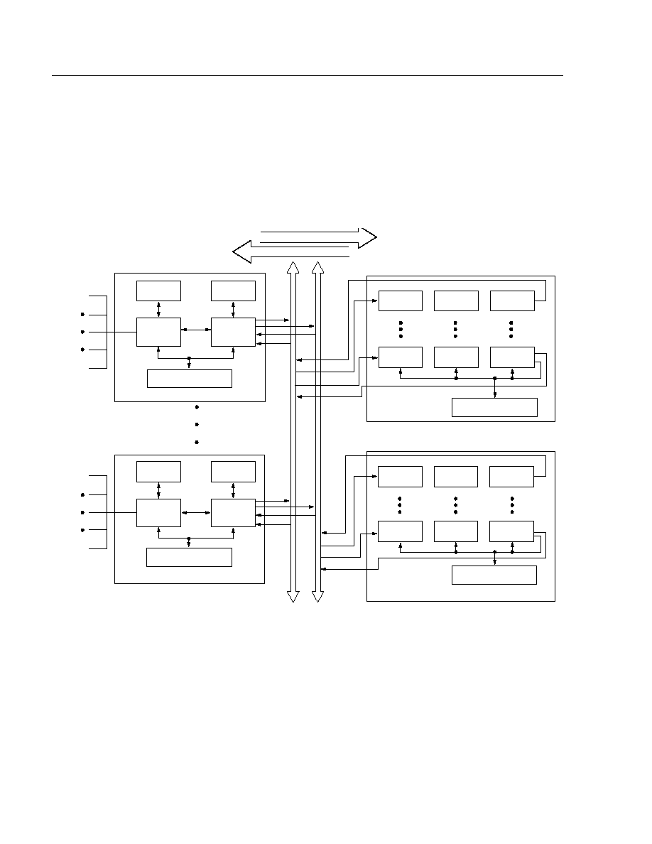
Figure 1 shows the architecture of an ATM switch
designed with the ATLANTA chip set. The LUC4AU01
ATM UNI Layer Manager (ALM) chip performs the ATM
layer network interface (UNI or NNI) management func-
tions for an MPHY line card and can be programmed to
work with proprietary ATM switch fabric cores.
The ALM operates in a full-duplex manner, with a max-
imum ATM cell traffic rate of 662 Mbits/s in each direc-
tion. The ingress side processes cells arriving from the
UNI; the egress side processes cells being sent to the
UNI.
5-4554r9
Figure 1. Architecture of an ATM Switch Using the ATLANTA Chip Set
ALM
LUC4AU01
MICROPROCESSOR
INTERFACE
SRAM
LINE CARD #1
#1
#1
LINE CARD #N
N x N SWITCH FABRIC
#N
BA
CKPLANE
REDUND
ANT BA
CKPLANE
ABM
LUC4AB01
SRAM
PHYSICAL LAYER
INTERFACE (MPHY)
ALM
LUC4AU01
SRAM
ABM
LUC4B01
SRAM
ASX
LUC4AS01
ACE
LUC4AC01
ASX
LUC4AS01
ASX
LUC4AS01
ACE
LUC4AC01
ASX
LUC4AS01
#1
#1
#N
N x N REDUNDANT SWITCH FABRIC
#N
ASX
LUC4AS01
ACE
LUC4AC01
ASX
LUC4AS01
ASX
LUC4AS01
ACE
LUC4AC01
ASX
LUC4AS01
#1
#1
#N
INGRESS DIRECTION
EGRESS DIRECTION
#1
#1
#N
#N
#N
#N
1
M
PHY PORTS
1
M
PHY PORTS
MICROPROCESSOR
INTERFACE
MICROPROCESSOR
INTERFACE
MICROPROCESSOR
INTERFACE

Lucent Technologies Inc.
3
Preliminary Product Brief
March 1997
ATM Layer UNI Manager (ALM)
LUC4AU01
Section 5.2
LUCENT TECHNOLOGIES--PROPRIETARY
Use pursuant to Company Instructions
Description
(continued)
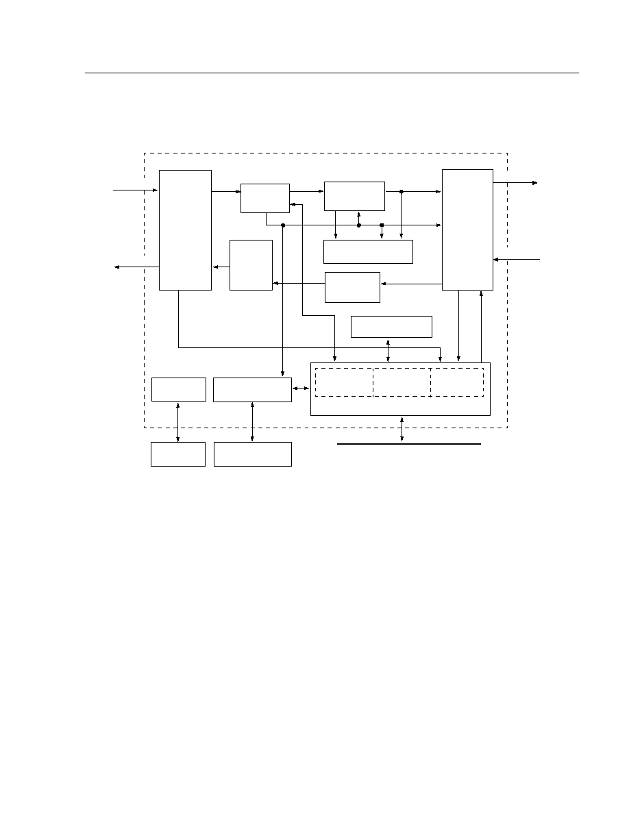
The block diagram of the chip and a brief description of the functionality of each block follows.
5-4611r3
Figure 2. ALM Block Diagram
UTOPIA
MPHY
INTERFACE
(UMI)
LOOK-UP
UNIT (LU)
POLICING UNIT
(POL)
MPHY PORT
(SPF)
STATISTICS COUNTERS
(CNT)
BUFFER
MANAGER
INTERFACE
(BMI)
HEADER
TRANSLATION
UNIT (HTU)
CONFIGURATION
REGISTERS (FIG)
TEST ACCESS
PORT (JTAG)
EXTERNAL MEMORY
INTERFACE (EMI)
INGRESS
CAPTURE FIFO
EGRESS
CAPTURE FIFO
INSERTION
FIFO
MICROPROCESSOR INTERFACE (MPI)
MICROPROCESSOR BUS
SYNCHRONOUS
ALM IC
INGRESS
EGRESS
INGRESS
EGRESS
UTOPIA II PLUS
INTERFACE
(TO/FROM
ATM FABRIC,
UTOPIA II
INTERFACE
(TO/FROM
LAYER)
PHYSICAL
FIFO
SRAM
TEST ACCESS
PORT
e.g., LUC4AB01
ABM)

4
4
Lucent Technologies Inc.
Preliminary Product Brief
March 1997
ATM Layer UNI Manager (ALM)
LUC4AU01
Section 5.2
LUCENT TECHNOLOGIES--PROPRIETARY
Use pursuant to Company Instructions
Description
(continued)
UTOPIA MPHY Interface (UMI)
The UMI controls the transfer of ATM cells between the
ALM and multiple physical layer devices (MPHYs) con-
nected to ALM via the UTOPIA Level II MPHY inter-
face.
The chip transmits and receives ATM cells via a pair of
16-bit wide buses, using cell-level handshake flow con-
trol for up to 30 UNIs or NNIs. The UMI also checks
header errors (HEC) on the ingress cells and inserts a
locally calculated HEC into the egress cells. Cells
received with incorrect HEC are either corrected or
dropped depending on the appropriate setting in the
configuration register.
Look Up Unit (LU)
Based on the incoming VPI and VCI, the look-up unit
performs a two-level look up to fetch connection infor-
mation (from external memory) for an ingress cell. It
supports range check on VPI and VCI. The VPI and VCI
values of ingress cells are checked against maximum
values for an active connection set up. Cells with invalid
VPI or VCI values are dropped or captured depending
on the settings in the configuration registers. The look-
up unit also recognizes OA&M and ABR RM cells
received on ingress by examining the first two bytes of
the cell payload.
Policing Unit (POL)
The policing unit checks ingress cells for conformance
to their negotiated traffic contracts.
It uses the ATM Forum-compliant dual leaky-bucket
algorithm to determine if the cell should be tagged or
dropped. Policing can be enabled or disabled on a per-
VP basis, as well as globally enabled or disabled. The
policing action, tag or drop, can be programmed sepa-
rately for each individual leaky bucket on a per-connec-
tion basis.
Statistics Counters (CNT)
This block maintains per-connection 31-bit statistic
counters for the ingress and egress cells. These
counters are stored in external memory. They can be
written or read through the microprocessor interface.
The statistics feature can be globally enabled or dis-
abled. There are six counters available for each con-
nection (four for ingress, two for egress).
Microprocessor Interface (MPI)
The MPI allows an external processor to access the
ALM for configuration, maintenance, and internal and
external memory reads and writes (e.g., for call set or
tear down). It provides a 16-bit asynchronous interface
to
Intel
,
Motorola
, or generic microprocessors. It also
generates an interrupt when status bits are set.
Configuration Registers (FIG)
The configuration registers store all user-programma-
ble values. They allow the external microprocessor to
control the following, for example: to enable/disable
global statistics gathering, policing, HEC correction,
and generation of time slot synchronization signal. It
also allows configuration of base addresses for tables
in external memory for policing parameters, translation,
VC parameters, and counters. It is also used to deter-
mine the size of prepended local routing headers.
External Memory Interface (EMI)
The external memory interface is responsible for
accessing external memory (composed of synchro-
nous SRAMs). It is used for scheduling accesses and
sends control signals for ALM internal functions or
microprocessor-requested operations (e.g., call setup
or tear down, collect statistics). The ALM supports a
32-bit wide interface to synchronous SRAMs (20 ns
cycle time, nonpipelined, registered input), with a maxi-
mum depth of 512 Kwords.
Buffer Module Interface (BMI)
The BMI manages the UTOPIA II Plus ingress and
egress data buses and control signals to allow for com-
munication between the ALM and an external buffer
manager/module (e.g., the LUC4AB01 ATM Buffer
Manager, ABM, device) on the ATM layer (switch) side
of ALM. The BMI optionally captures and routes man-
agement cells to a microprocessor accessible FIFO.
The BMI inserts cell identification bits (OA&M flows,
forward and backward ABR RM, and policing outcome
as conforming/nonconforming in the local routing
header.

Lucent Technologies Inc.
5
Preliminary Product Brief
March 1997
ATM Layer UNI Manager (ALM)
LUC4AU01
Section 5.2
LUCENT TECHNOLOGIES--PROPRIETARY
Use pursuant to Company Instructions
Description
(continued)
Header Translation Unit (HTU)
The HTU performs ATM header translation on egress
cells. It supports up to 64K egress VCs and can option-
ally translate (for NNI) or pass (for UNI) the GFC field of
the ATM header.
MPHY Port FIFOs (SPF)
This block consists of FIFOs that temporarily store out-
going egress cells before their delivery to the destina-
tion MPHY ports on UTOPIA II or the microprocessor-
accessible egress capture FIFO.
Test Access Port (JTAG)
The ALM incorporates logic to support a standard five-
pin test access port (TAP), compatible with the
IEEE
P1149.1 standard (JTAG), used for boundary scan.
TAP contains instruction registers, data registers, and
control logic, and has its own set of instructions. It is
controlled externally by a JTAG bus master. The TAP
gives the ALM board-level test capability.

Preliminary Product Brief
March 1997
ATM Layer UNI Manager (ALM)
LUC4AU01
For additional information, contact your Microelectronics Group Account Manager or the following:
INTERNET:
http://www.lucent.com/micro
U.S.A.: Microelectronics Group, Lucent Technologies Inc., 555 Union Boulevard, Room 30L-15P-BA, Allentown, PA 18103
1-800-372-2447
, FAX 610-712-4106 (In CANADA:
1-800-553-2448
, FAX 610-712-4106), e-mail
docmaster@micro.lucent.com
ASIA PACIFIC:
Microelectronics Group, Lucent Technologies Singapore Pte. Ltd., 77 Science Park Drive, #03-18 Cintech III, Singapore 118256
Tel. (65) 778 8833
, FAX (65) 777 7495
JAPAN: Microelectronics Group, Lucent Technologies Japan Ltd., 7-18, Higashi-Gotanda 2-chome, Shinagawa-ku, Tokyo 141, Japan
Tel. (81) 3 5421 1600
, FAX (81) 3 5421 1700
For data requests in Europe:
MICROELECTRONICS GROUP DATALINE:
Tel. (44) 1734 324 299
, FAX (44) 1734 328 148
For technical inquiries in Europe:
CENTRAL EUROPE:
(49) 89 95086 0
(Munich), NORTHERN EUROPE:
(44) 1344 865 900
(Bracknell UK),
FRANCE:
(33) 1 41 45 77 00
(Paris), SOUTHERN EUROPE:
(39) 2 6601 1800
(Milan) or
(34) 1 807 1700
(Madrid)
Lucent Technologies Inc. reserves the right to make changes to the product(s) or information contained herein without notice. No liability is assumed as a result of their use or application. No
rights under any patent accompany the sale of any such product(s) or information.
Copyright © 1997 Lucent Technologies Inc.
All Rights Reserved
Printed in U.S.A.
March 1997
PN96-064ATM
Printed On
Recycled Paper
