Preliminary Data Sheet
August 1998
LUCDA4044 Phase Frequency Detector
Features
s
Typical propagation delay 9.0 ns (through phase
detector)
s
Includes charge pump and amplifier
s
Available in 14-pin DIP or SONB
12-3519F
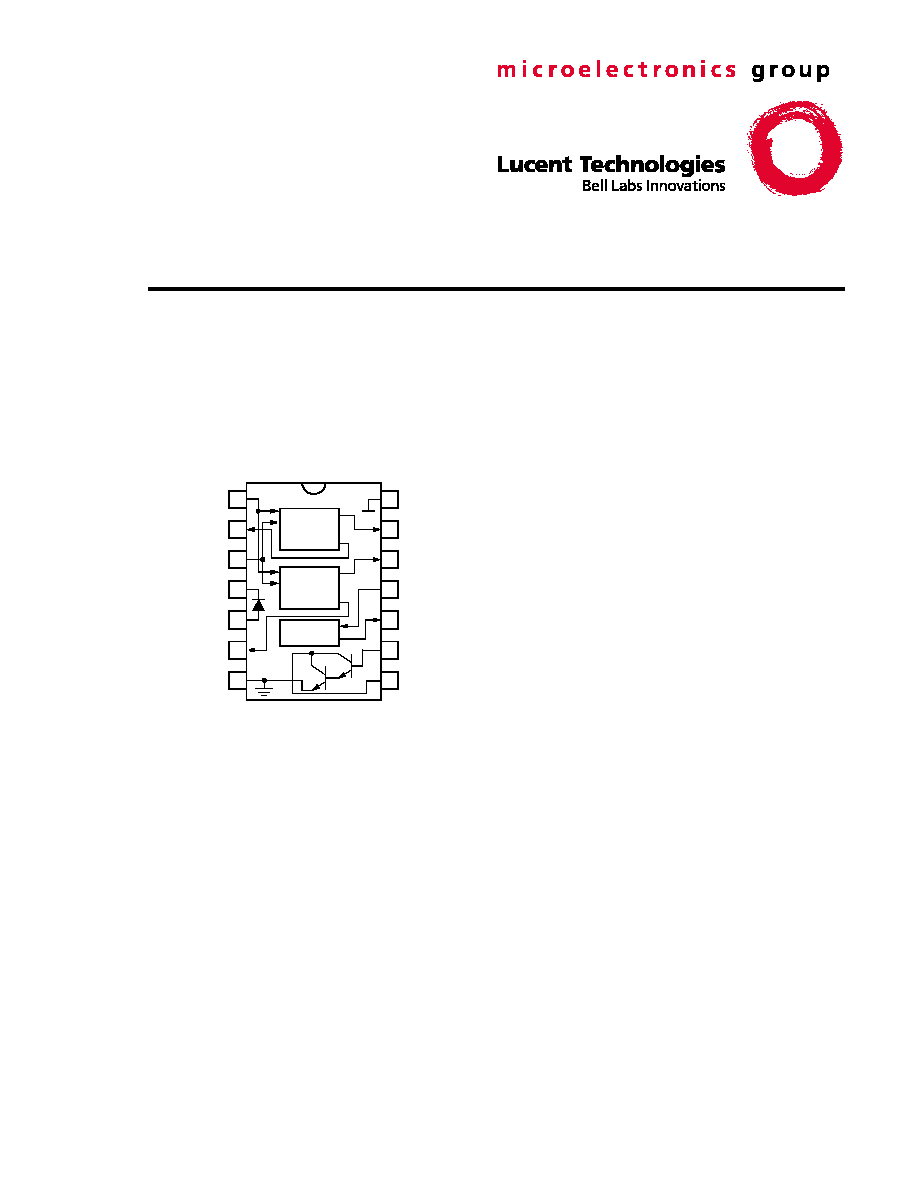
Figure 1. Functional Diagram
Applications
s
Frequency synthesizers
s
Clock recovery
Description
The LUCDA4044 consists of two digital phase detec-
tors, a charge pump, and an amplifier. In combination
with a voltage-controlled multivibrator, this device is
useful in a broad range of phase-locked loop (PLL)
applications. The circuit accepts TTL waveforms at
the R and V inputs and generates an error voltage
that is proportional to frequency and/or phase differ-
ence.
Phase detector #1 is intended for use in systems
requiring zero frequency and phase at lock. Phase
detector #2 is used if quadrature lock is desired.
Phase detector #2 can also be used to indicate that
the main loop (utilizing phase detector #1) is out of
lock. This LUCDA4044 is a direct replacement for the
Motorola* MC4044.
*
Motorola is a registered trademark of Motorola Inc.
1
2
3
4
5
6
7
14
13
12
11
10
9
8
PU
R
D1
V
UF
D2
GND
PD
V
CC
U1
U2
DF
AIN
AOU
PHASE
FREQUENCY
DETECTOR
#1
PHASE
FREQUENCY
DETECTOR
#2
CHARGE
PUMP
2
2
Lucent Technologies Inc.
Preliminary Data Sheet
August 1998
LUCDA4044 Phase Frequency Detector
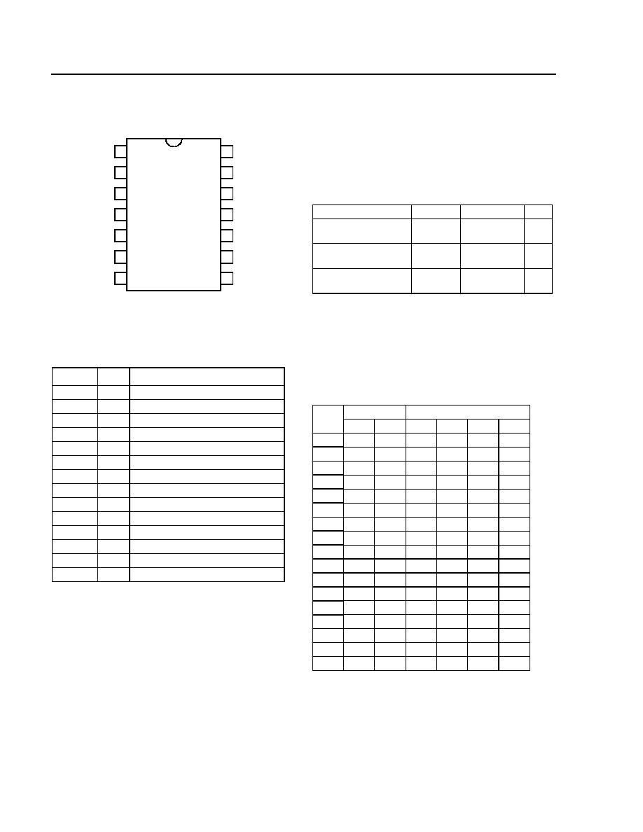
Pin Information
12-3518F
Figure 2. Pin Diagram
Table 1. Pin Descriptions
Absolute Maximum Ratings
Stresses in excess of the absolute maximum ratings
can cause permanent damage to the device. These are
absolute stress ratings only. Functional operation of the
device is not implied at these or any other conditions in
excess of those given in the operational sections of the
data sheet. Exposure to absolute maximum ratings for
extended periods can adversely affect device reliability.
Truth Table
This table is not strictly a functional truth table; i.e., it
does not show all possible modes of operation. It is
included as an aid for dc testing.
Table 2. Truth Table
Notes:
x indicates output state unknown.
U1 and D1 outputs are sequential, i.e., they must be sequenced in
the order shown.
U2 and D2 outputs are combinational, i.e., they need only inputs to
obtain the desired output state.
Symbol
Pin
Description
1
R
Common Reference Signal Input
2
D1
Detector #1 Output
3
V
Common Variable Signal Input
4
PU
Diode Cathode
5
UF
Diode Anode
6
D2
Detector #2 Output
7
GND Power Supply Ground
8
AOU Amplifier Output
9
AIN
Amplifier Input
10
DF
Charge Pump Output
11
PD
Charge Pump Input
12
U2
Detector #2 Output
13
U1
Detector #1 Output
14
V
CC
Positive Power Supply
1
2
3
4
5
6
7
14
13
12
11
10
9
8
PU
R
D1
V
UF
D2
GND
PD
V
CC
U1
U2
DF
AIN
AOU
Parameter
Symbol
Value
Unit
Ambient Operating
Temperature
--
≠40 to +85
∞
C
Storage Tempera-
ture Range
T
stg
≠40 to +125
∞
C
Power Supply Volt-
age (V
CC
to GND)
--
7.0
V
Input
State
Input
Output
R
V
U1
D1
U2
D2
1
0
0
x
x
1
1
2
1
0
x
x
0
1
3
1
1
x
x
1
0
4
1
0
x
x
0
1
5
0
0
x
x
1
1
6
1
0
x
x
0
1
7
0
0
0
1
1
1
8
1
0
0
1
0
1
9
0
0
0
1
1
1
10
0
1
0
1
1
1
11
0
0
1
1
1
1
12
0
1
1
1
1
1
13
0
0
1
0
1
1
14
0
1
1
0
1
1
15
0
0
1
0
1
1
16
1
0
1
0
0
1
17
0
0
1
1
1
1

Lucent Technologies Inc.
3
Preliminary Data Sheet
August 1998
LUCDA4044 Phase Frequency Detector
Electrical Characteristics
Table 3. Electrical Characteristics (at 25
∞
C)
* Pins 2 and 13 are prone to change state; care must be taken during testing.
Parameter
Symbol
Test Conditions
Min
Typ
Max
Unit
Output Voltage High (pins 2, 6, 12, 13)
V
OH
I
OH
= ≠1.6 mA
V
CC
= 4.75 V
2.4
--
--
V
Output Voltage Low (pins 2, 6, 12, 13)
V
OL
I
OL
= 16 mA
V
CC
= 4.75 V
--
--
0.4
V
Input Voltage High (pins 1, 3, 11)
V
IH
V
CC
= 4.75 V
2.0
--
--
V
Input Voltage Low (pins 1, 3, 11)
V
IL
V
CC
= 4.75 V
--
--
0.8
V
Input Current Low #1 (pins 1 and 3)
I
IL1
V
IL
= 0.4 V
V
CC
= 5.25 V
--
--
≠2.4
mA
Input Current Low #2 (pin 11)
I
IL2
V
IL
= 0.4 V
V
CC
= 5.25 V
--
--
≠0.8
mA
Input Current High #1 (pins 1 and 3)
I
IH1
V
IH
= 2.4 V
V
CC
= 5.25 V
--
--
120
µA
Input Current High #2 (pin 11)
I
IH2
V
IH
= 2.4 V
V
CC
= 5.25 V
--
--
40
µA
Input Current High (pins 1, 3, 11)
I
IHH
V
IH
= 5.25 V
V
CC
= 5.25 V
--
--
1.0
mA
Clamp Voltage (pins 1, 3, 11)
Vclamp
I
IN
= ≠18 mA
V
CC
= 4.75 V
--
--
≠1.5
V
Output Current (pins 2, 6, 12, 13)
I
OS
V
OL
= 0 V*
V
CC
= 5.25 V
≠30
--
≠85
mA
Forward Diode Voltage (pin 5)
V
DF
I
IN
= 1 mA
V
CC
= 5.25 V
0.4
--
1.0
V
Reverse Diode Voltage (pin 4)
V
DR
I
IN
= 5 µA
V
CC
= 5.25 V
5.25
--
--
V
Output Voltage High (pin 10)
V
OH
I
OH
= ≠1 mA
V
CC
= 4.75 V
2.5
--
--
V
Output Voltage Low (pin 10)
V
OL
I
OL
= 100 µA
V
CC
= 4.75 V
--
0
V
Output Current (pin 8)
I
OLK
V
A
= 0 V
V
CC
= 5.25 V
--
120
µA
Output Current (pin 8)
I
O
I
A
= 10 µA
V
CC
= 5.25 V
5.25
--
--
mA

4
Lucent Technologies Inc.
Preliminary Data Sheet
August 1998
LUCDA4044 Phase Frequency Detector
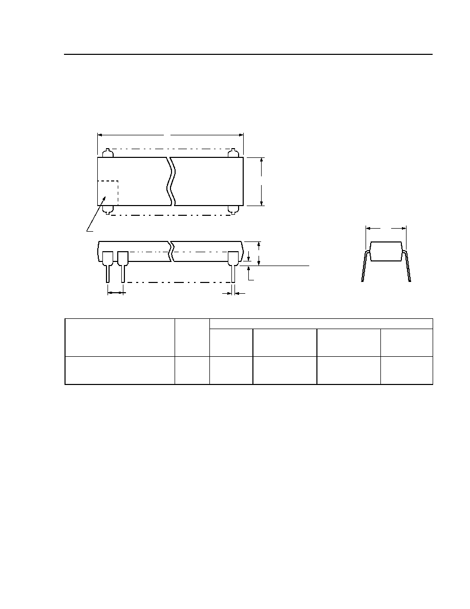
Outline Diagrams
14-Pin SONB
Dimensions are in millimeters.
5-4414F
Package
Description
Number of Pins
"N"
Package Dimensions
Maximum
Length "L"
Maximum Width
Without Leads
"B"
Maximum Width
Including Leads
"W"
Maximum
Height Above
Board
"H"
SONB
(Small Outline
Narrow Body)
14
8.84
4.01
6.17
1.73
W
0.61
0.51 MAX
H
0.28 MAX
0.10
SEATING PLANE
1.27 TYP
N
L
B
1
PIN #1 IDENTIFIER ZONE
Lucent Technologies Inc.
5
Preliminary Data Sheet
August 1998
LUCDA4044 Phase Frequency Detector
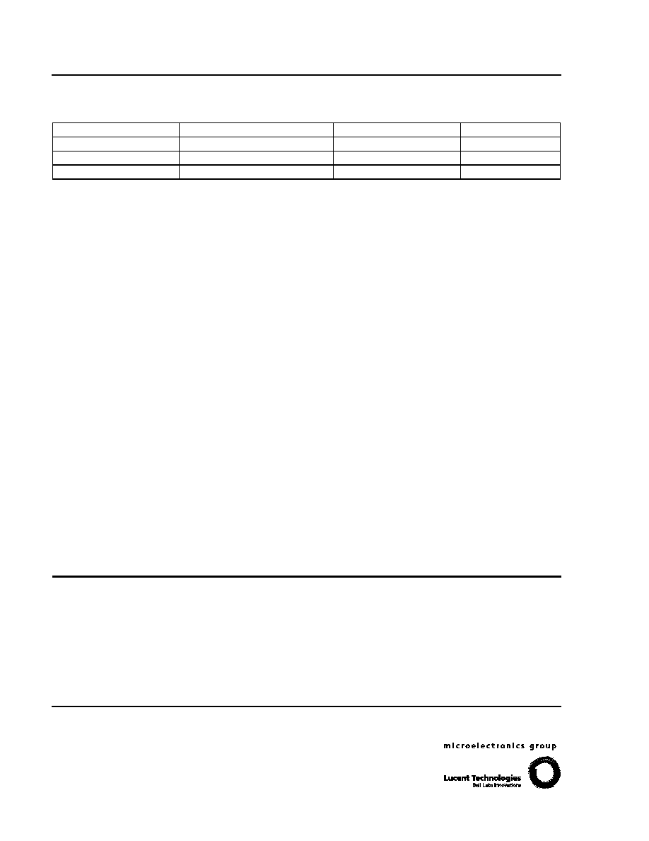
Outline Diagrams
(continued)
14-Pin DIP
Dimensions are in millimeters.
5-4410F
Package Description
Number
of
Pins
"N"
Package Dimensions
Maximum
Length
"L"
Maximum Width
Without Leads
"B"
Maximum Width
Including Leads
"W"
Maximum
Height Above
Board "H"
PDIP3
(Plastic Dual Inline Package)
(0.300" Series)
14
20.57
6.47
7.87
5.08
W
H
0.58 MAX
2.54 TYP
0.38 MIN
SEATING PLANE
N
1
PIN #1 IDENTIFIER ZONE
L
B
Preliminary Data Sheet
August 1998
LUCDA4044 Phase Frequency Detector
Lucent Technologies Inc. reserves the right to make changes to the product(s) or information contained herein without notice. No liability is assumed as a result of their use or application. No
rights under any patent accompany the sale of any such product(s) or information.
Copyright © 1998 Lucent Technologies Inc.
All Rights Reserved
Printed in U.S.A.
August 1998
DS98-390LEG
For additional information, contact your Microelectronics Group Account Manager or the following:
INTERNET:
http://www.lucent.com/micro
E-MAIL:
docmaster@micro.lucent.com
N. AMERICA:
Microelectronics Group, Lucent Technologies Inc., 555 Union Boulevard, Room 30L-15P-BA, Allentown, PA 18103
1-800-372-2447, FAX 610-712-4106 (In CANADA: 1-800-553-2448, FAX 610-712-4106)
ASIA PACIFIC: Microelectronics Group, Lucent Technologies Singapore Pte. Ltd., 77 Science Park Drive, #03-18 Cintech III, Singapore 118256
Tel. (65) 778 8833, FAX (65) 777 7495
CHINA:
Microelectronics Group, Lucent Technologies (China) Co., Ltd., A-F2, 23/F, Zao Fong Universe Building, 1800 Zhong Shan Xi Road,
Shanghai 200233 P. R. China Tel. (86) 21 6440 0468, ext. 316, FAX (86) 21 6440 0652
JAPAN:
Microelectronics Group, Lucent Technologies Japan Ltd., 7-18, Higashi-Gotanda 2-chome, Shinagawa-ku, Tokyo 141, Japan
Tel. (81) 3 5421 1600, FAX (81) 3 5421 1700
EUROPE:
Data Requests: MICROELECTRONICS GROUP DATALINE: Tel. (44) 1189 324 299, FAX (44) 1189 328 148
Technical Inquiries: GERMANY: (49) 89 95086 0 (Munich), UNITED KINGDOM: (44) 1344 865 900 (Bracknell),
FRANCE: (33) 1 48 83 68 00 (Paris), SWEDEN: (46) 8 600 7070 (Stockholm), FINLAND: (358) 9 4354 2800 (Helsinki),
ITALY: (39) 2 6608131 (Milan), SPAIN: (34) 1 807 1441 (Madrid)
Ordering Information
Device Code
Package
Operating Temperature
Comcode
LUCDA4044AAFE
14-Pin SONB
≠40 to +85
108158403
LUCDA4044AAFE-TR
14-Pin SONB Tape and Reel
≠40 to +85
108158411
LUCDA4044AAPE
14-Pin DIP
≠40 to +85
108158429