Preliminary Data Sheet
September 2001
L7585F Full-Feature, Low-Power SLIC and Switch
Features
s
Low active power
s
Quiet tip/ring polarity reversal
s
Distortion-free on-hook transmission
s
35 V to 60 V power supply operation
s
14 operating states:
-- Forward battery active
-- Reverse battery active
-- Ground start (3)
-- Forward battery ring open
-- Reverse battery ring open
-- Reverse battery tip open
-- High impedance
-- Ringing (2)
-- Low current (2)
-- Disconnect
s
Self-test in all operating states
s
Independent, adjustable ac and dc parameters:
-- Switchhook detector threshold
-- Loop current limit
-- dc feed resistance
-- Termination impedance
s
Integrated ringing access relay
s
Integrated test-in relay
s
Integrated relay driver
s
Integrated ring trip detector
s
Thermal protection
s
44-pin, surface-mount, plastic package (PLCC)
Description
The L7585F Full-Feature, Low-Power Subscriber
Loop Interface Circuit (SLIC) and Switch integrates
the battery feed, test access relay, and ringing relay
that are necessary to interface a codec to the tip and
ring of a subscriber loop into one low-power, low-cost
package. It is built using a 90 V complementary bipo-
lar (CBIC) process and a 320 V Bipolar-CMOS-
DMOS (BCDMOS) process. The device is available
in a 44-pin PLCC package.
The device can be connected directly to the Agere
Systems Inc. T8531/T8532 16-Channel Programma-
ble Codec Chip Set without the need for any ac inter-
face components.

2
Agere Communications Inc.
Data Sheet
September 2001
L7585F Full-Feature, Low-Power SLIC and Switch
Table of Contents
Contents
Page
Features ......................................................................1
Description...................................................................1
Architectural Diagram ..................................................3
Pin Information ............................................................4
Operating States..........................................................7
Forward Battery Active State ....................................7
Ground Start/Tip Open State ....................................7
Ground Start/Tip Ground State .................................8
Forward Battery Ring Open State .............................8
Ringing States (2) .....................................................8
Disconnect State .......................................................8
Forward Battery Low-Current Active State ...............8
High-Impedance States (2) .......................................8
Reverse Battery Active State ....................................8
Reverse Battery Tip Open State ...............................8
Ground Start/Tip Amplifier State ...............................9
Reverse Battery Ring Open State.............................9
Reverse Battery Low-Current Active State ...............9
Absolute Maximum Ratings (T
A
= 25 ∞C).....................9
Electrical Characteristics ...........................................10
On-State Switch V-I Characteristics ..........................17
Applications ...............................................................18
Tip/Ring Protection .................................................18
NDET Under Fault Conditions ................................18
Power, Clocking, and Layout ..................................18
Ring Trip .................................................................19
False On-Hook Transients ......................................19
Application Diagram ..................................................20
Outline Diagram.........................................................21
44-Pin PLCC ...........................................................21
Ordering Information .................................................22
Figures
Page
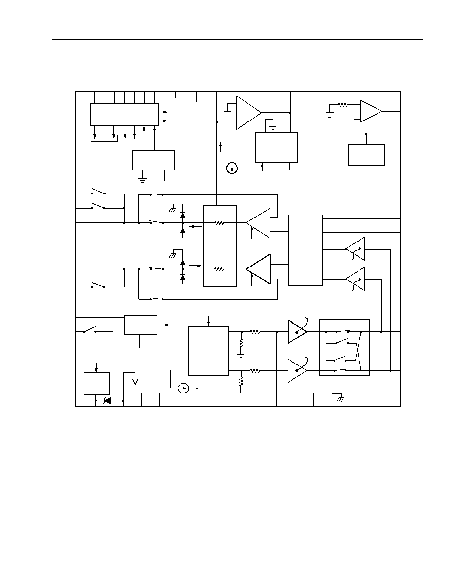
Figure 1. Architectural Diagram ................................. 3
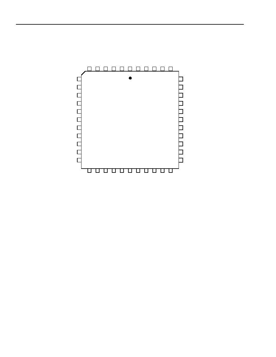
Figure 2. 44-Pin Diagram (PLCC) ............................. 4
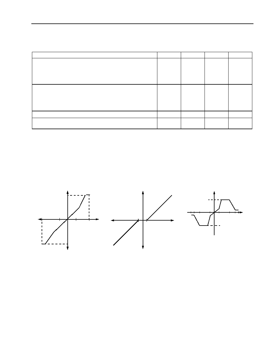
Figure 3. On-State Switch V-I Characteristics ......... 17
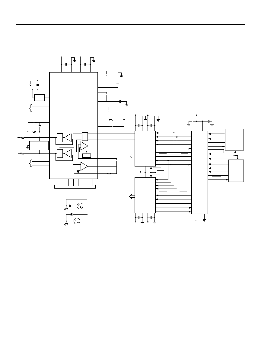
Figure 4. 16-Channel Line Card Solution ................ 20
Tables
Page
Table 1. Pin Descriptions ........................................... 5
Table 2. B0--B3 Input State Coding .......................... 7
Table 3. B4--B5 Input State Coding .......................... 7
Table 4. Operating Conditions and Powering .......... 10
Table 5. Ring Trip Detector ..................................... 10
Table 6. Battery Feed Characteristics ..................... 11
Table 7. Analog Signal Pins .................................... 12
Table 8. Transmission Characteristics .................... 13
Table 9. Data Interface and Logic (Logic Inputs
[CLK, NCS, and B0--B5] and
Outputs [NDET]) ........................................ 14
Table 10. Timing Requirements (CLK, B0--B5,
and NCS) ................................................. 14
Table 11. Relay Driver (RDO) ................................. 14
Table 12. Ringing Return Access Switch (SW1) ..... 15
Table 13. Test-In Access Switches
(SW3 and SW6) ....................................... 15
Table 14. Tip and Ring Break Switches
(SW2 and SW4) ....................................... 16
Table 15. Tip and Ring Feedback Switches
(SW2a and SW4a) ................................... 16
Table 16. Ringing Access Switch (SW5) ................. 17

Agere Communications Inc.
3
Data Sheet
September 2001
L7585F Full-Feature, Low-Power SLIC and Switch
Architectural Diagram
12-3290.e(F)
Figure 1. Architectural Diagram
RFT
20
TIP/RING
CURRENT
SENSE
RFR
20
V
BAT
V
BAT
NPDAT
NPDAR
TRNG
TTI
PT
PR
RTI
RING TRIP
DETECTOR
SW5
RD
RELAY
DRIVER
NRT
RSW
RTS
RRNG
dc
FEEDBACK
AND
CURRENT
LIMIT
DC
OUT
ac
INTERFACE
V
BAT
BUFFER
BUFFER
RDO
DGND
V
CCD
V
SP
I
PROG
DCR
CF2 CF1
V
BAT
BGND
BUFFER
BUFFER
ac
dc
V
BAT
FB2
FB1
RCVN
RCVP
AR
+
≠
75
µ
A
PARALLEL DATA LATCH
AND LOGIC
SWITCHHOOK
DETECTOR
NCS B5 B4 B3 B2 B1 B0
CLK
NDET
RD FB NRT
NLC
SW1--SW6
CONTROL
+
≠
AGND
V
CCA
SW1
45
LCTH
DC
OUT
VRTX
VTX
2.4 V
REFERENCE
TXI
VITR
ITR
AAC
REF
IN
RECTIFIER
GAIN = 3
OUT
AX
+
≠
50
µ
A
+5 A
ITR
ITR
AT
≠
+
+5 A
NPDAT
NPDAR
FB
100 k
ITR/198
SW3
45
GTO
+5 A
+5 D
+10 V
SW6
SW4
SW4a
SW2a
4 k
SW2
25

4
Agere Communications Inc.
Data Sheet
September 2001
L7585F Full-Feature, Low-Power SLIC and Switch
Pin Information
12-2571(F).f
Figure 2. 44-Pin Diagram (PLCC)
I
PR
O
G
DGND
V
CCD
B0
B1
B2
BGND
FB1
FB2
V
BAT
V
SP
NCS
NDET
DGND
7
9
10
11
12
13
14
15
16
17
8
6
4
3
2
1
44
43
42
41
40
5
18
20
21
22
23
24
25
26
27
28
19
39
37
36
35
34
33
32
31
30
29
38
V
BAT
B3
V
BAT
BGND
ITR
VITR
TXI
CF1
CLK
AG
N
D
V
CCA
RCV
N
RCV
P
VR
T
X
LCTH
VT
X
DC
OUT
DCR
CF2
B4
TRNG
RTS
PR
B5
PT
TTI
RT
I
RRNG
RSW
RDO

Agere Communications Inc.
5
Data Sheet
September 2001
L7585F Full-Feature, Low-Power SLIC and Switch
Pin Information
(continued)
Table 1. Pin Descriptions
Note: On the printed-wiring board (PWB), make the leads to BGND and V
BAT
as wide as possible for thermal and electrical reasons. Also, max-
imize the amount of PWB copper on all leads connected to this device for the lowest operating temperature.
Pin
Symbol
Type
Name/Function
1
V
CCA
--
+5 V Analog dc Supply. +5 V supply for analog circuitry.
2
LCTH
I
Loop Closure Threshold Input. Connect a resistor to DC
OUT
to set the off-hook thresh-
old.
3
I
PROG
I
Current-Limit Program Input. A resistor to DC
OUT
sets the dc current limit.
4
DC
OUT
O
dc Output. This output is a voltage that is directly proportional to the differential
tip/ring current.
5
DCR
I
dc Resistance. Ground for dc feed resistance of 180
, or short to DC
OUT
for 600
. In-
termediate values can be set with a resistor divider from DC
OUT
to ground, the tap of which
is connected to DCR.
6
CF2
I/O
Filter Capacitor 2. Connect a 0.1 µF, 100 V capacitor from this pin to AGND and a
0.22 µF, 100 V capacitor from this pin to pin CF1.
7
CF1
I/O
Filter Capacitor 1. Connect a 0.22 µF, 100 V capacitor from this pin to pin CF2.
8
FB2
I
Forward Battery Slowdown 2. A capacitor from FB1 to AGND and from FB2 to AGND
will ramp the polarity reversal transition when quiet polarity reversal is required. If not
needed, the pin can be left open.
9
FB1
I
Forward Battery Slowdown 1. A capacitor from FB1 to AGND and from FB2 to AGND
will ramp the polarity reversal transition when quiet polarity reversal is required. If not
needed, the pin can be left open.
10
BGND
--
Battery Ground. Ground return for the battery (V
BAT
) supply.
11
V
BAT
--
Battery Supply. Negative high-voltage power supply.
12
V
BAT
--
Battery Supply. Negative high-voltage power supply.
13
V
SP
--
+10 V Supply. +10 V bias supply for switch circuitry.
14
NCS
I
Not Channel Select. A low-to-high transition on this logic input stores the data on pins
B0--B5 into the input latches on the SLIC. When NCS is either high or low, the SLIC is
unaffected by data on pins B0--B5.
15
CLK
I
Clock. Clock input.
16
NDET
O
Not Detect. When low, this logic output indicates either a ring trip or an off-hook condition,
depending on the input state of the SLIC. If either the BCDMOS portion or CBIC portion
of this device enters thermal shutdown, NDET will be forced low.
17
DGND
--
Digital Ground. Ground return for V
CCD
and relay driver flyback current.
18
RDO
O
Relay Driver. This output drives an external relay. RDO is low (relay operated) when a
low input on B5 is latched into the SLIC.
19
RTS
I
Ring Trip Sense. Sense input for the ring trip detector.
20
RSW
O
Ring Lead Ringing Access Switch. Ringing relay connects this pin to pin RRNG. Con-
nect this pin to pin PR through a 500
current-limiting resistor.
21
RRNG
I
Ring Lead Ringing Supply. Connect this pin to the ringing supply.
22
PR
I/O
Protected Ring. The output of the ring driver and input to the transmit current sense cir-
cuit. Connect to the ring of the loop through overvoltage protection.

6
Agere Communications Inc.
Data Sheet
September 2001
L7585F Full-Feature, Low-Power SLIC and Switch
Pin Information
(continued)
Table 1. Pin Descriptions (continued)
Note: On the printed-wiring board (PWB), make the leads to BGND and V
BAT
as wide as possible for thermal and electrical reasons. Also, max-
imize the amount of PWB copper on all leads connected to this device for the lowest operating temperature.
Pin Symbol
Type
Name/Function
23
RTI
I
Ring Lead Test-In. Test-in relay connects this pin to PR. Connect RTI to the ring lead of
the test-in bus.
24
TTI
I
Tip Lead Test-In. Test-in relay connects this pin to PT. Connect TTI to the tip lead of the
test-in bus.
25
PT
I/O
Protected Tip. The output of the tip driver and input to the transmit current sense circuit.
Connect to the tip of the loop through overvoltage protection.
26
TRNG
O
Tip Lead Ringing Supply. Ringing relay connects this pin to PT. Connect TRNG to the
ringing supply return.
27
B5
I
Bit 5. B0--B5 determine the state of the SLIC. See Operating States.
28
B4
I
Bit 4. B0--B5 determine the state of the SLIC. See Operating States.
29
B3
I
Bit 3. B0--B5 determine the state of the SLIC. See Operating States.
30
B2
I
Bit 2. B0--B5 determine the state of the SLIC. See Operating States.
31
B1
I
Bit 1. B0--B5 determine the state of the SLIC. See Operating States.
32
B0
I
Bit 0. B0--B5 determine the state of the SLIC. See Operating States.
33
V
CCD
--
+5 V Digital dc Supply. +5 V supply for logic and switch circuitry.
34
DGND
--
Digital Ground. Ground return for V
CCD
.
35
V
BAT
--
Battery Supply. Negative high-voltage power supply.
36
BGND
--
Battery Ground. Ground return for the battery (V
BAT
) supply.
37
ITR
I
Tip/Ring Current. A current output which is proportional to the differential current flowing
from tip to ring. Connect a resistor from this pin to VITR.
38
VITR
O
Tip/Ring Voltage Output. The voltage at this output is directly proportional to the differ-
ential tip/ring current. A resistor from this pin to ITR sets the gain.
39
TXI
I
Transmit ac Input. Connect a 0.1 µF capacitor from this pin to VITR.
40
VTX
O
Transmit ac Output Voltage. The ac voltage at this output is 7.2 times the ac voltage at
pin TXI. The dc voltage is equal to the dc voltage on pin VRTX.
41
VRTX
O
Transmit ac Reference Voltage. The dc voltage at this output (2.4 V nominal) is the dc
reference for the transmit signal output VTX.
42
RCVP
I
Receive ac Signal Input (Noninverting). This high-impedance input controls the ac dif-
ferential voltage on tip and ring.
43
RCVN
I
Receive ac Signal Input (Inverting). This high-impedance input controls the ac differen-
tial voltage on tip and ring.
44
AGND
--
Analog Ground. Ground return for V
CCA
.

Agere Communications Inc.
7
Data Sheet
September 2001
L7585F Full-Feature, Low-Power SLIC and Switch
Operating States
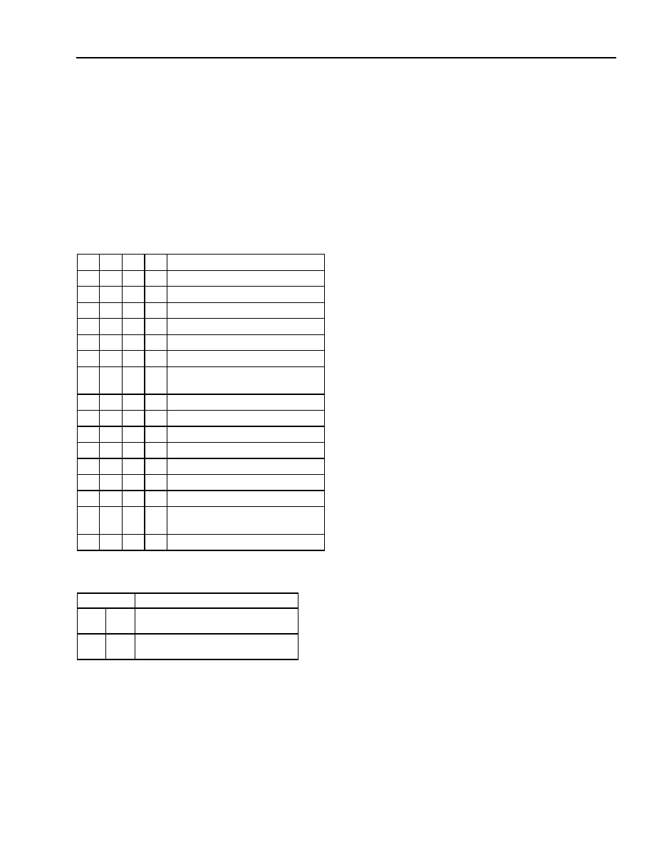
The L7585 has 13 operating states. These states are
selected using 4 bits, B0--B3, according to the truth
table shown in Table 2. The operation of the L7585 is
undefined for unassigned states. Additionally, bit B4
independently operates the test-in access contacts so
that all states are available for self-test; and bit B5
independently operates a relay driver, regardless of the
status of bits B0--B4. All 6 bits are loaded via the par-
allel data interface and chip select lead NCS.
Table 2. B0--B3 Input State Coding
Table 3. B4--B5 Input State Coding
Forward Battery Active State
s
Normal talk and forward battery feed state.
s
All circuits are powered up and active.
s
Pin PT is positive with respect to pin PR (forward bat-
tery).
s
SW2, SW2a, SW4, and SW4a closed; SW1, SW3,
SW5, and SW6 open.
s
NDET reflects the status of the switchhook detector.
Ground Start/Tip Open State
s
Ground start idle supervision state.
s
Ring lead continuity test state (tone injected at the
receive port) in forward battery.
s
Same as forward battery active state, but with SW2
and SW2a open, and the tip drive amplifier powered
down.
s
Pin PT is high impedance (>100 k
).
s
The ring current limit is approximately equal to the
value programmed for the high-current active state
current limit. Current limit is achieved by reducing the
ring lead voltage only (see Table 6).
s
NDET indicates an off-hook when the ring current
(flowing into PR) is twice the value programmed for
the switchhook detector in the forward battery active
state.
B3 B2 B1 B0
State
1
1
1
1
Forward Battery Active
1
1
1
0
Ground Start/Tip Open
1
1
0
1
Ground Start/Tip Ground
1
1
0
0
Forward Battery Ring Open
1
0
1
1
Ringing (Battery Backed)
1
0
1
0
Disconnect State
1
0
0
1
Forward Battery Low Current
Active State
1
0
0
0
High Impedance
0
1
1
1
Reverse Battery Active
0
1
1
0
Reverse Battery Tip Open
0
1
0
1
Ground Start/Tip Amplifier
0
1
0
0
Reverse Battery Ring Open
0
0
1
1
Ringing (Earth Backed)
0
0
1
0
Unassigned
0
0
0
1
Reverse Battery Low-Current
Active State
0
0
0
0
High Impedance
Bit
State
B4
1
Test-in contacts off.
0
Test-in contacts on.
B5
1
Relay driver off.
0
Relay driver on.

8
8
Agere Communications Inc.
Data Sheet
September 2001
L7585F Full-Feature, Low-Power SLIC and Switch
Operating States
(continued)
Ground Start/Tip Ground State
s
Ground start busy supervision state.
s
Same as ground start/tip open state but with SW1
closed.
Forward Battery Ring Open State
s
Tip lead continuity test state (tone injected at the
receive port) in forward battery.
s
Same as forward battery active state, but with SW4
and SW4a open, and the ring drive amplifier
powered down.
s
Pin PR is high impedance (>100 k
).
s
Tip current limit is twice the low-current active state
current limit.
s
NDET indicates an off-hook when the tip current
(flowing out of PT) is twice the value programmed for
the switchhook detector in the forward battery active
state.
Ringing States (2)
s
Normal ringing state.
s
Tip and ring drive amplifiers are powered down.
s
SW1 and SW5 closed; SW2, SW2a, SW3, SW4,
SW4a, and SW6 open.
s
NDET reflects the status of the ring trip detector.
s
Bit B3 indicates whether the ringing voltage applied
to the ringing bus is either battery backed (B3 = 1) or
earth backed (B3 = 0). Although B3 has no direct
effect on the state of the SLIC, it can be used by the
ring trip detector to enhance ring trip detection.
Disconnect State
s
All circuits are powered up and active.
s
SW2, SW2a, SW4, and SW4a closed; SW1, SW3,
SW5, and SW6 open.
s
PT and PR are at the same potential to deny current
to the loop.
Forward Battery Low-Current Active State
s
Normal talk and forward battery feed state.
s
All circuits are powered up and active.
s
Pin PT is positive with respect to pin PR (forward bat-
tery).
s
SW2, SW2a, SW4, and SW4a closed; SW1, SW3,
SW5, and SW6 open.
s
NDET reflects the status of the switchhook detector.
s
Current limit is lowered to approximately 0.66 times
the normal limit.
High-Impedance States (2)
s
Disconnect state.
s
Tip and ring drive amplifiers are powered down (all
bias currents off).
s
Pins PT and PR are high impedance (>100 k
).
s
SW1, SW2, SW2a, SW3, SW4, SW4a, SW5, and
SW6 open.
s
NDET is undefined.
Reverse Battery Active State
s
Normal talk and reverse battery feed state.
s
Same as forward battery active state, but PR is posi-
tive with respect to PT.
Reverse Battery Tip Open State
s
Ring lead continuity test state (tone injected at the
receive port) in reverse battery.
s
SW2 and SW2a open and the tip drive amplifier pow-
ered down.
s
Pin PT is high impedance (>100 k
).
s
Pin PR is held between -1.7 V and -2.3 V for PR cur-
rents less than +-20 mA. PR current limit is the SW4
break switch current limit (250 mA < I < 85 mA).
s
NDET indicates an off-hook when the ring current
(flowing out of PR) is twice the value programmed for
the switchhook detector in the reverse battery active
state.

Agere Communications Inc.
9
Data Sheet
September 2001
L7585F Full-Feature, Low-Power SLIC and Switch
Operating States
(continued)
Ground Start/Tip Amplifier State
s
Current limiting is achieved by reducing ring lead
voltage only. This state is the same as Ground Start/
Tip Open, but with SW2 and SW2A closed and the
tip amplifier powered up.
s
Ring lead current limit is approximately the difference
of the high-current active state limit and the current
flowing out of the tip lead.
s
On-hook transmission not to exceed ≠3 dBm with up
to 5 mA flowing out of the tip lead (maximum current
flow into the tip lead is permissible). Larger signal
and/or current may cause distortion.
s
NDET indicates an off-hook when the current flowing
out of the tip plus the current flowing into the ring is
twice the value programmed for the switchhook
detector.
Reverse Battery Ring Open State
s
Tip lead continuity test state (tone injected at the
receive port) in reverse battery.
s
Same as reverse battery active state, but with SW4
and SW4a open, and the ring drive amplifier
powered down.
s
Pin PR is high impedance (>100 k
).
s
Tip current limit is twice the low-current active state
current limit.
s
NDET indicates an off-hook when the tip current
(flowing into PT) is twice the value programmed for
the switchhook detector in the reverse battery active
state.
Reverse Battery Low-Current Active State
s
Normal talk and reverse battery feed state.
s
Same as forward battery active state, but PR is posi-
tive with respect to PT.
s
Current limit is lowered to approximately 0.66 times
the normal limit.
Absolute Maximum Ratings
(T
A
= 25 ∞C)
Stresses exceeding the values listed under absolute
maximum ratings may cause permanent damage to the
device. This is an absolute stress rating only. Func-
tional operation of the device at these or any other con-
ditions in excess of those indicated in the operational
sections of this data sheet is not implied. Exposure to
absolute maximum rating conditions for extended peri-
ods of time may adversely affect device reliability.
Note:
Analog voltages are referenced to AGND, digital (logic) volt-
ages are referenced to DGND, and battery voltages are ref-
erenced to BGND. The IC can be damaged unless all
ground connections are applied before and are removed
after all other connections. Furthermore, when powering the
device, the user must guarantee that no external potential
creates a voltage on any pin of the device that exceeds the
device ratings. Some of the known examples of conditions
that cause such potentials during powering are the following:
1) an inductor connected to tip and ring that can force an
overvoltage on V
BAT
through external components if the
V
BAT
connection chatters; and 2) inductance in the V
BAT
lead that could resonate with the V
BAT
filter capacitor to
cause a destructive overvoltage.
Parameter
Value
Unit
+5 V dc Supplies (V
CCA
and
V
CCD
)
≠0.5 to +7.0
V
+10 V dc Bias Supply (V
SP
)
≠0.5 to +15
V
Office Battery Supply (V
BAT
)
≠63 to +0.5
V
Logic Input Voltage
≠0.5 to
V
DDD
+ 0.5
V
Logic Input Clamp Diode Cur-
rent, per Pin
±20
mA
Logic Output Voltage
≠0.5 to
V
DDD
+ 0.5
V
Logic Output Current, per Pin
(excluding relay driver)
±35
mA
Operating Temperature Range
≠40 to +125
∞C
Storage Temperature Range
≠40 to +125
∞C
Relative Humidity Range
5 to 95
%RH
Ground Potential Difference
(BGND to AGND)
±3
V
Ground Potential Difference
(DGND to AGND)
±3
V

10
Agere Communications Inc.
Data Sheet
September 2001
L7585F Full-Feature, Low-Power SLIC and Switch
Electrical Characteristics
In general, minimum and maximum values are testing requirements. However, some parameters may not be
tested in production because they are guaranteed by design and device characterization. Typical values reflect the
design center or nominal value of the parameter; they are for information only and are not a requirement. Minimum
and maximum values apply across the entire temperature range (≠40 ∞C to +85 ∞C) and entire battery range
(≠35 V to ≠60 V). Unless otherwise specified, typical is defined as 25 ∞C, V
CCA
= +5.0 V, V
CCD
= +5.0 V,
V
SP
= +10 V, V
BAT
= ≠48 V. Positive currents flow into the device.
* Not to exceed 26 grams of water per kilogram of dry air.
This parameter is not tested in production; it is guaranteed by design and device characterization.
1. The ringing source may be either of the following:
a). The ringing source consists of the ac and dc voltages added together (battery-backed ringing); the ringing return is ground. In this case,
bit B3 will always be a 1 when ringing is applied.
b). The ringing source consists of only the ac voltage (earth-backed ringing); the ringing return is the dc voltage. In this case, bit B3 will
always be a 0 when ringing is applied.
2. NDET must also indicate ring trip when the ac ringing voltage is absent (<5 Vrms) from the ringing source.
3. Pretrip ringing must not be tripped by a 10 k
resistor in parallel with an 8 µF capacitor applied across tip and ring.
Table 4. Operating Conditions and Powering
Parameter
Min
Typ
Max
Unit
Temperature Range
≠40
--
85
∞C
Humidity Range
5
--
95*
%RH
Supply Voltages:
V
CCA
V
CCD
V
SP
V
BAT
V
CCA
--V
CCD
D
GND
--A
GND
4.75
4.75
8.0
≠35
--
--
5.0
5.0
10
≠48
--
--
5.5
5.5
12.0
≠60
±0.5
±0.25
V
V
V
V
V
V
Supply Currents (all states, no loop current):
I
CCA
+ I
CCD
(+5 V)
IV
SP
(+10 V)
I
BAT
(≠48 V)
--
--
--
4.9
45
≠3.1
7.0
200
≠4.0
mA
µA
mA
Total Power Dissipation (all states, no loop current)
(V
CC
= +5 V; V
SP
= +10 V; V
BAT
= ≠48 V)
--
175
200
mW
Power Supply Rejection (tip/ring and transmit)
:
V
CCA
(500 Hz--3 kHz; 50 mVrms ripple)
V
CCD
(500 Hz--3 kHz; 50 mVrms ripple)
V
SP
(500 Hz--3 kHz; 250 mVrms ripple)
V
BAT
(500 Hz--3 kHz; 50 mVrms ripple)
30
45
45
45
40
--
--
--
--
--
--
--
dB
dB
dB
dB
Thermal
:
Thermal Resistance (still air)
Operating T
JC
--
--
--
--
47
155
∞C/W
∞C
Table 5. Ring Trip Detector
Parameter
Min
Typ
Max
Unit
Voltage at input that will cause ring trip after appropriate zero crossings.
±2.5
±3
±3.5
V
Voltage at input that will cause immediate ring trip.
±12
±15
±18
V
Ringing Source
1
:
Frequency (f)
dc Voltage
ac Voltage
19
≠39.5
60
20
--
--
28
≠57
105
Hz
V
Vrms
Ring Trip (NDET = 0)
2, 3
:
Loop Resistance
Trip Time
NDET Valid
2000
--
--
--
--
--
--
200
80
ms
ms

Agere Communications Inc.
11
Data Sheet
September 2001
L7585F Full-Feature, Low-Power SLIC and Switch
Electrical Characteristics
(continued)
Table 6. Battery Feed Characteristics
1. The longitudinal current is independent of dc loop current.
2.
Current limit, I
LIM
, is programmed by a resistor, R
PROG
, from pin I
PROG
to pin DC
OUT
. R
PROG
= 1.667 x (I
LIM
≠ 4); R
PROG
in k
and I
LIM
in mA. The current limit versus loop voltage has a slope of 10 k
. The low current mode current limit is approximately 0.66 times the high
current limit. The ground start ring lead ground current limit is approximately equal to the high current limit and has a slope of about 5 k
.
3. In transmission applications, for compliance with TR-57, ground start ring lead I-V characteristics at high battery, it is expected that the
high-current active current limit will be set to 28 mA.
4. Loop closure detector current, I
LCD
, is programmed by a resistor, RLCTH, from pin LCTH to pin DC
OUT
. RLCTH = 2.5 x I
LCD
; RLCTH in
k
and I
LCD
in mA. I
LCD
is the tip to ring (forward battery) or ring to tip (reverse battery) current at which the loop closure detector indi-
cates an off-hook.
5. dc feed resistance may be adjusted between 180
and 600
using a resistor divider between DC
OUT
and DCR. The open loop differen-
tial voltage may also be increased by applying a negative voltage to pin DCR. See dc Gains, pin DCR.
6. DC
OUT
gain depends on the resistor RGX1 from pin VITR to pin ITR. This gain assumes 8250
, the recommended value. Positive current
is defined as the differential current flowing from PT to PR.
7. Positive voltage on pin DCR has no effect on the PT/PR voltage.
8. At tip and ring, assuming 82.5
protection resistors.
9. At tip and ring with matched 82.5
protection resistors when feedback is connected for either 600
or 900
termination impedance.
Parameter
Symbol
Min
Typ
Max
Unit
Tip or Ring Drive Current =
dc + Longitudinal + Signal Currents
--
65
--
--
mA
ac Signal Current
--
10
--
--
mArms
Longitudinal Current Capability per Wire
1
--
8.5
15
--
mArms
dc Loop Current Limit
2
(R
LOOP
= 100
):
I
LIM
Programmability Range
5
--
45
mA
Current Limit with V
BAT
= ≠51.5 V
and R
PROG
= 64.9 k
44
42
56
mA
Low-current Mode
2
(R
LOOP
= 100
,
V
BAT
= ≠51.5 V, and R
PROG
= 64.9 k
)
25
27.5
30
mA
Ground Start Ring Grounded (R
LOOP
= 100
)
Current Limit
3
:
V
BAT
= ≠51.5 V, R
PROG
= 64.9 k
38
43
47
mA
Loop Closure Current Detector Threshold
4
Programming Accuracy
I
LCD
--
--
±7
%
Open Loop Voltages (DCR = 0 V):
Common-mode Voltage
Differential Voltage
--
--
|V
BAT
+ 7.0|
(V
BAT
+ 1.8)/2
|V
BAT
+ 6.5|
--
|V
BAT
+ 6.0|
V
V
Disconnect State PT/PR Voltage
|PT-PR|
--
--
±100
mV
Ground Start Ring Lead Open or Shorted to Ground:
PT and CF1 Voltage
--
≠1.7
≠2.0
≠2.3
V
dc Feed Resistance:
DCR Grounded
DCR Connected to DC
OUT
5
--
130
480
150
505
170
630
dc Gains:
PT/PR Current to DC
OUT
Voltage
6
:
Forward Battery
Reverse Battery
DCR Voltage
7
to PT/PR Differential Voltage
--
≠118
118
3.13
--
--
3.33
≠132
132
3.53
V/A
V/A
--
Loop Resistance Range
8
(3.17 dBm overload into 600
):
I
LOOP
= 20 mA at V
BAT
= ≠51.5 V
--
1890
1930
--
Longitudinal to Metallic Balance--
IEEE
Æ
Std. 455:
50 Hz to 1 kHz
1 kHz to 3 kHz
--
58
9
48
70
66
--
--
dB
dB
Metallic to Longitudinal (harm) Balance:
200 Hz to 4 kHz
--
35
--
--
dB

12
Agere Communications Inc.
Data Sheet
September 2001
L7585F Full-Feature, Low-Power SLIC and Switch
Electrical Characteristics
(continued)
Table 7. Analog Signal Pins
1. This parameter is not tested in production; it is guaranteed by design and device characterization.
2. VTX offset is measured with respect to pin VRTX.
3. Positive voltages from 0 V to V
CCA
are permitted at input DCR; however, voltages above 0 V have no effect on either the dc feed resis-
tance or tip/ring voltage.
Parameter
Min
Typ
Max
Unit
DC
OUT
:
Output Offset (no loop current)
Output Drive Current
Output Voltage Swing (+0.25 mA/≠3 mA load):
Maximum
Minimum
Output Short-circuit Current
Output Load Resistance
Output Load Capacitance
1
--
0.25
V
BAT
≠10
--
5
--
--
--
--
--
--
--
--
±200
≠3.0
V
CCA
0.5
±20
--
50
mV
mA
V
V
mA
k
pF
VITR and VTX:
Output Offset (no loop current)
2
Output Drive Current
Output Voltage Swing (±1 mA load):
Maximum
Minimum (VITR)
Minimum (VTX)
Output Short-circuit Current
Output Load Resistance
Output Load Capacitance
1
--
±1
≠10
±3.5
≠3.5
--
4
--
--
--
--
--
--
--
--
--
±100
--
V
CCA
--
V
CCA
≠ 1.0
±20
--
50
mV
mA
V
V
V
mA
k
pF
VRTX:
Output Voltage
Output Drive Current
Output Short-circuit Current
Output Load Capacitance
1
2.2
±500
--
--
2.4
--
--
--
2.6
--
±15
50
V
µA
mA
pF
RSW:
Impedance to Ground
3
--
--
M
DCR:
Input Voltage Range
3
Input Bias Current
Input Impedance
≠8
--
500
--
--
--
0
±1
--
V
µA
k
TXI:
Input Impedance
Input Voltage Compliance
Input Clamp Voltage
75
±0.4
±0.4
--
--
--
--
--
±0.8
k
V
V
RCVP and RCVN:
Input Voltage Range
Input Bias Current
Input Impedance
≠2.5
--
10
--
--
--
V
CCA
±1.5
--
V
µA
M
PT and PR:
Overvoltage (from external source; continuous)
--
--
±265
V
FB1 and FB2:
ac Output Impedance
Output Short-circuit Current
--
±27
--
--
10
±34
k
µA
CF1 and CF2:
Output Impedance
1
180
--
375
k

Agere Communications Inc.
13
Data Sheet
September 2001
L7585F Full-Feature, Low-Power SLIC and Switch
Electrical Characteristics
(continued)
Transmit direction is tip/ring to VTX. Receive direction is RCVP(N) to tip/ring.
Table 8. Transmission Characteristics
1. Set by external components in conjunction with the T7531A/T7536 codecs. Any complex impedance R1 + R2 || C between 200
and
1200
can be synthesized.
2. Return loss and transhybrid loss are functions of device gain accuracies and the external hybrid circuit. Guaranteed performance assumes
1% tolerance external resistors and capacitors.
3. This parameter is not tested in production; it is guaranteed by design and device characterization.
4. VTX gain depends on the resistor RGX1 from pin VITR to pin ITR. This gain assumes an ideal 8250
, the recommended value. Positive cur-
rent is defined as the differential current flowing from PT to PR. The transmit signal at VTX is measured with respect to pin VRTX.
Parameter
Min
Typ
Max
Unit
ac Termination Impedance
1
200
--
1200
Return Loss
2
:
200 Hz--500 Hz
500 Hz--3400 Hz
25
29
--
--
--
--
dB
dB
Total Harmonic Distortion (200 Hz--4 kHz)
3
:
Off-hook
On-hook
--
--
--
--
0.3
1
%
%
Transmit Gain (f = 1 kHz)
4
:
PT/PR Current to (VTX--VRTX)
≠291
≠300
≠309
V/A
Receive Gain (f = 1 kHz):
(RCVP--RCVN) to (PT--PR)
1.94
2
2.06
--
Gain vs. Frequency (transmit and receive)
3
(600
termination; 1 kHz reference):
200 Hz--300 Hz
300 Hz--3.4 kHz
3.4 kHz--20 kHz
20 kHz--266 kHz
≠0.3
≠0.05
≠3.0
--
0
0
0
--
0.05
0.05
0.05
2.0
dB
dB
dB
dB
Gain vs. Level (transmit and receive; 0 dBV reference)
3
:
≠50 dB to +3 dB
≠0.05
0
0.05
dB
Transhybrid Loss
2
:
200 Hz--500 Hz
500 Hz--3400 Hz
25
29
--
--
--
--
dB
dB
Idle-channel Noise (tip/ring; 600
termination):
Psophometric
C-message
3 kHz Flat
--
--
--
--
--
--
≠77
13
20
dBmp
dBrnC
dBrn
Idle-channel Noise ((VTX--VRTX); 600
termination):
Psophometric
C-message
3 kHz Flat
--
--
--
--
--
--
≠77
13
20
dBmp0
dBrnC0
dBrn0
EMC, per EN 300 386-2 and EN61000-4-6 (3 Vrms, 80% mod-
ulation, 105 kHz--80 MHz, 150
source impedance)
3
--
--
≠40
dBm, 600

14
Agere Communications Inc.
Data Sheet
September 2001
L7585F Full-Feature, Low-Power SLIC and Switch
Electrical Characteristics
(continued)
Table 9. Data Interface and Logic (Logic Inputs [CLK, NCS, and B0--B5] and Outputs [NDET])
1. Unless otherwise specified, all logic voltages are referenced to DGND.
2. This parameter is not tested in production; it is guaranteed by design and device characterization.
Table 10. Timing Requirements (CLK, B0--B5, and NCS)
1, 2
1. Unless otherwise specified, all times are measured from the 50% point of logic transitions.
2. These parameters are not tested in production; they are guaranteed by design and device characterization.
Table 11. Relay Driver (RDO)
1. Unless otherwise specified, all logic voltages are referenced to DGND.
2. This parameter is not tested in production; it is guaranteed by design and device characterization.
Parameter
1
Symbol
Min
Max
Unit
High-level Input Voltage
V
IH
2
V
CCD
V
Low-level Input Voltage
V
IL
0
0.8
V
Input Bias Current (high and low)
I
IN
--
±10
µA
High-level Output Voltage (I
OUT
= ≠100 µA)
V
OH
V
CCD
≠ 1.5
V
CCD
V
Low-level Output Voltage (I
OUT
= 180 µA)
V
OL
0
0.4
V
Output Short-circuit Current (V
OUT
= V
CCD
)
I
OSS
1
35
mA
Output Load Capacitance
2
C
OL
0
50
pF
Parameter
Symbol
Min
Max
Unit
CLK and NCS Rise and Fall Time (10% to 90%)
tR, tF
0
50
ns
Maximum Input Capacitance
CIN
--
5
pF
Minimum Setup Time from B0--B5 Valid to NCS
V
IH
= 2 V
V
IH
= 2.5 V
tSDS
tSDS
250
150
--
--
ns
ns
Minimum Hold Time from NCS to B0--B5 Not Valid
V
IH
= 2 V
V
IH
= 2.5 V
tHDS
tHDS
150
10
--
--
ns
ns
Minimum Pulse Width of NCS
tWCS
195
--
ns
CLK Frequency
fCLK
0.9
2.2
MHz
Minimum Pulse Width of CLK
tWCK
195
--
ns
Parameter
1
Symbol
Min
Max
Unit
Off-state Output Current (V
RDO
= V
CCD
)
I
OFF
--
±10
µA
On-state Output Voltage (I
RDO
= 40 mA)
V
ON
0
0.60
V
On-state Output Voltage (I
RDO
= 20 mA)
V
ON
0
0.40
V
Clamp Diode Reverse Current (V
RDO
= 0)
I
R
--
±10
µA
Clamp Diode On Voltage (I
RDO
= 80 mA)
V
OC
6
20
V
Turn-on Time
2
t
ON
--
10
µs
Turn-off Time
2
t
OFF
--
10
µs

Agere Communications Inc.
15
Data Sheet
September 2001
L7585F Full-Feature, Low-Power SLIC and Switch
Electrical Characteristics
(continued)
Table 12. Ringing Return Access Switch (SW1)
1. At 25 ∞C, maximum voltage rating has a temperature coefficient of +0.167 V/∞C.
2. This parameter is not tested in production; it is guaranteed by design and device characterization.
3. Applied voltage is 100 Vp-p square wave at 100 Hz to measure dV/dt sensitivity at 200 V/µs typical with no switch turn-on. In the case of
dV/dt induced turn-on at higher dV/dt and amplitude, the design objective is no damage to at least 2000 V/µs and full voltage. A known con-
dition that can cause damage is initial current flow prior to the application of the dV/dt and the sudden application of reverse bias with dV/dt
induced switch turn-off. In this case, no damage shall occur for dV/dt up to 2000 V/µs as guaranteed by design and characterization.
Table 13. Test-In Access Switches (SW3 and SW6)
1. At 25 ∞C, maximum voltage rating has a temperature coefficient of +0.167 V/∞C.
2. This parameter is not tested in production; it is guaranteed by design and device characterization.
3. Test in access switches current limit will be > tip and ring break switches current limit.
4. Applied voltage is 100 Vp-p square wave at 100 Hz to measure dV/dt sensitivity at 200 V/µs typical with no switch turn-on. In the case of
dV/dt induced turn-on at higher dV/dt and amplitude, the design objective is no damage to at least 2000 V/µs and full voltage. A known con-
dition that can cause damage is initial current flow prior to the application of the dV/dt and the sudden application of reverse bias with dV/dt
induced switch turn-off. In this case, no damage shall occur for dV/dt up to 2000 V/µs as guaranteed by design and characterization.
Parameter
Min
Typ
Max
Unit
Off-state:
Maximum Differential Voltage
dc Leakage Current (V
SW
= ±320 V)
Feedthrough Capacitance
2
--
--
--
--
--
--
±320
1
±10
15
V
µA
pF
On-state (See On-State Switch V-I Characteristics section.):
Resistance (R
ON
)
Maximum Differential Voltage (V
max
)
Foldback Voltage Breakpoint 1 (V
1
)
Foldback Voltage Breakpoint 2 (V
2
)
Current Limit (I
LIMIT1
)
Current Limit (I
LIMIT2
)
--
--
120
200
120
2
45
--
--
--
220
--
90
320
1
--
--
360
--
V
V
V
mA
mA
dV/dT Sensitivity
2, 3
--
200
2000
V/µs
Parameter
Min
Typ
Max
Unit
Off-state:
Maximum Differential Voltage
dc Leakage Current (V
SW
= ±320 V)
Feedthrough Capacitance
2
--
--
--
--
--
--
±320
1
±10
15
V
µA
pF
On-state (See On-State Switch V-I Characteristics section.):
Resistance (R
ON
)
Maximum Differential Voltage (V
max
)
Current Limit (I
LIMIT
) Switches SW3 and SW6
3
--
--
85
45
--
--
90
60
--
V
mA
dV/dT Sensitivity
2, 4
--
200
2000
V/µs

16
Agere Communications Inc.
Data Sheet
September 2001
L7585F Full-Feature, Low-Power SLIC and Switch
Electrical Characteristics
(continued)
Table 14. Tip and Ring Break Switches (SW2 and SW4)
1. At 25 ∞C, maximum voltage rating has a temperature coefficient of +0.167 V/∞C.
2. This parameter is not tested in production; it is guaranteed by design and device characterization.
3. Applied voltage is 100 Vp-p square wave at 100 Hz to measure dV/dt sensitivity at 200 V/µs typical with no switch turn-on. In the case of
dV/dt induced turn-on at higher dV/dt and amplitude, the design objective is no damage to at least 2000 V/µs and full voltage. A known con-
dition that can cause damage is initial current flow prior to the application of the dV/dt and the sudden application of reverse bias with dV/dt
induced switch turn-off. In this case, no damage shall occur for dV/dt up to 2000 V/µs as guaranteed by design and characterization.
Table 15. Tip and Ring Feedback Switches (SW2a and SW4a)
1. At 25 ∞C, maximum voltage rating has a temperature coefficient of +0.167 V/∞C.
2. This parameter is not tested in production; it is guaranteed by design and device characterization.
3. Applied voltage is 100 Vp-p square wave at 100 Hz to measure dV/dt sensitivity at 200 V/µs typical with no switch turn-on. In the case of
dV/dt induced turn-on at higher dV/dt and amplitude, the design objective is no damage to at least 2000 V/µs and full voltage. A known con-
dition that can cause damage is initial current flow prior to the application of the dV/dt and the sudden application of reverse bias with dV/dt
induced switch turn-off. In this case, no damage shall occur for dV/dt up to 2000 V/µs as guaranteed by design and characterization.
Parameter
Min
Typ
Max
Unit
Off-state:
Maximum Differential Voltage
dc Leakage Current (V
SW
= ±320 V)
Feedthrough Capacitance
2
--
--
--
--
--
--
±320
1
±20
50
V
µA
pF
On-state (See On-State Switch V-I Characteristics section.):
Resistance (R
ON
)
Maximum Differential Voltage (V
max
)
Foldback Voltage Breakpoint 1 (V
1
)
Foldback Voltage Breakpoint 2 (V
2
)
Current Limit (I
LIMIT1
)
Current Limit (I
LIMIT2
)
--
--
60
V
1
+ 0.5
85
2
25
--
--
--
160
--
50
320
1
--
--
250
--
V
V
V
mA
mA
dV/dT Sensitivity
2, 3
--
200
2000
V/µs
Parameter
Min
Typ
Max
Unit
Off-state:
Maximum Differential Voltage
dc Leakage Current (V
SW
= ±320 V)
Feedthrough Capacitance
2
--
--
--
--
--
--
±320
1
±10
15
V
µA
pF
On-state (See On-State Switch V-I Characteristics section.):
Resistance (R
ON
)
Maximum Differential Voltage (V
max
)
Current Limit (I
LIMIT
)
--
--
0.5
4
--
--
10
320
1
20
k
V
mA
dV/dT Sensitivity
2, 3
--
200
2000
V/µs

Agere Communications Inc.
17
Data Sheet
September 2001
L7585F Full-Feature, Low-Power SLIC and Switch
Electrical Characteristics
(continued)
Table 16. Ringing Access Switch (SW5)
1. This parameter is not tested in production; it is guaranteed by design and device characterization.
2. Applied voltage is 100 Vp-p square wave at 100 Hz to measure dV/dT sensitivity.
3. Applied voltage is 100 Vp-p square wave at 100 Hz to measure dV/dt sensitivity at 200 V/µs typical with no switch turn-on. In the case of
dV/dt induced turn-on at higher dV/dt and amplitude, the design objective is no damage to at least 2000 V/µs and full voltage. A known con-
dition that can cause damage is initial current flow prior to the application of the dV/dt and the sudden application of reverse bias with dV/dt
induced switch turn-off. In this case, no damage shall occur for dV/dt up to 2000 V/µs as guaranteed by design and characterization.
On-State Switch I-V Characteristics
Parameter
Min
Typ
Max
Unit
Off-state:
Maximum Differential Voltage
dc Leakage Current (V
SW
= ±500 V)
dc Leakage Current (V
SW
= ±250 V)
Feedthrough Capacitance
1
--
--
--
--
--
--
--
1
±475
±20
±1
--
V
µA
µA
pF
On-state (See On-State Switch V-I Characteristics section.):
Crossover Offset Voltage (V
OS
; ISW = ±1 mA)
Resistance (R
ON
)
Surge Current (10 µs x 1000 µs pulse)
1
Release Current
1
--
--
--
0.1
--
--
--
--
3
10
2.5
2
V
A
mA
dV/dT Sensitivity
1, 2
--
200
2000
V/µs
Common-mode Voltage (Maximum Either Switch Terminal with
Respect to Ground)
--
--
320
V
12-3291.a(F)
A. SW2a, SW3, SW4a, SW6
12-3292.a(F)
B. SW5
5-5990.c(F)
C. SW1, SW2, SW4
Figure 3. On-State Switch I-V Characteristics
≠V
MAX
≠I
LIMIT
+I
LIMIT
+V
MAX
V
SW
+1.5 V
≠1.5 V
R
ON
2/3 R
ON
CURRENT
LIMITING
I
SW
2/3 R
ON
CURRENT
LIMITING
≠V
OS
+V
OS
V
SW
R
ON
I
SW
R
ON
I
LIM1
I
SW
+1.5
2/3 R
ON
R
ON
≠1.5
≠I
LIM1
+V
MAX
V
SW
I
LIM2
≠I
LIM2
+V
2
+V
1
≠V
MAX
≠V
2
≠V
1

18
18
Agere Communications Inc.
Data Sheet
September 2001
L7585F Full-Feature, Low-Power SLIC and Switch
Applications
Tip/Ring Protection
The L7585 SLIC has integrated overvoltage tertiary
protection diodes in the tip and ring paths. The device
also has an integrated thermal shutdown circuit which
places tip/ring drivers in a high-impedance state when
the die temperature exceeds 160 ∞C.
The SLIC requires the following to survive lightning and
power cross requirements:
s
Fusible elements or PTCs
s
Current-limiting resistors
s
A secondary protector
Thermal fuse/surge resistor modules that satisfy the
various requirements can be purchased from
MMC
TM
.
Protection resistors should have a tolerance of ±1%
and a ratio tolerance of ±0.5%. The suppressor break-
over voltage of the secondary protector should be set
as low as possible. Select a value just above the maxi-
mum peak ring signal and maximum battery voltage.
NDET Under Fault Condition
s
The state of NDET is not guaranteed with loss of bat-
tery.
s
In the ringing state, RRNG floating or with only dc on
the ringing source, NDET will produce an off-hook
because there are not zero crossings of ringing to
cause an on-hook.
s
In the ringing state with only ac (>40 Vrms) on the
ringing source, an on-hook will be produced after the
second zero crossing of the ringing waveform,
because there is no dc component to the ringing cur-
rent.
s
In the ringing state, if the resistor between RSW and
PR is open, there will likely be a large voltage at the
ringing input (due to capacitive loading) and ring trip
will be asserted after the second zero crossing of
ringing. Because there is no guarantee of the load at
PR in this condition, there can be no guarantee of
the state on NDET in this condition.
s
If the device enters into thermal shutdown due to a
fault that causes an off-hook, the off-hook indication
will be stable as the device cycles in and out of ther-
mal shutdown. If the fault does not cause an off-
hook, NDET will cycle between on- and off-hook as
the device cycles in and out of thermal shutdown.
Power, Clocking, and Layout
The SLIC requires +5 V (V
CCA
and V
CCD
) and a nega-
tive battery voltage (V
BAT
) to operate. The integrated
switches require a 10 V or 12 V supply (V
SP
) and a TTL
clock (CLK) to operate. CLK requires a frequency
between 1.0 MHz to 2.048 MHz with a 50% duty cycle.
SW1, SW3, and SW6 will not operate without CLK
applied.
A four- or six-layer board is recommended. Analog and
battery grounds should be laid out as a plane and a
layer, and tied together at the device. Digital ground
can also be tied to this plane or run separately. V
SP
is
referenced to DGND. V
CC
can be run as individual
traces and can reside on the same layer as signal
paths. V
CCA
and V
CCD
can be tied together at the SLIC.
Placement of the talk battery is not critical.
The ring bus should be on a separate layer from the
SLIC/codec interface signal leads and traces should
run perpendicular if the traces must cross. TXI, VITR,
and ITR are the sensitive nodes on the SLIC. Transmit
runners should be run in pairs, and receive runners
should be run in pairs between the SLIC and the
codec. A channel-to-channel spacing should be main-
tained.

Agere Communications Inc.
19
Data Sheet
September 2001
L7585F Full-Feature, Low-Power SLIC and Switch
Applications
(continued)
Ring Trip
Ring trip is set by the value of RS1.
The ring trip threshold at the ring trip inputs is ±2.5 V
minimum, ±3.5 V maximum.
A resistor value of 500
, as shown in Figure 4, will set
the ring trip current threshold to ±6.0 mA typical.
Ring trip is asserted upon entering the ringing mode
until the second zero crossing of ringing. This is either
a positive-going zero crossing between ≠40 V and
≠30 V at ≠50 V V
BAT
) or a negative-going zero crossing
(between ≠10 V and ≠20 V at ≠50 V V
BAT
). The different
threshold for positive-going and negative-going zero
crossings is the result of hysteresis of approximately
20 V.
Ring trip will not be asserted unless the ring trip thresh-
old is exceeded for two zero crossings. This is either a
positive-going zero crossing between ≠40 V and ≠30 V
at ≠50 V V
BAT
) or a negative-going zero crossing
(between ≠10 V and ≠20 V at ≠50 V V
BAT
). The different
threshold for positive-going and negative-going zero
crossings is the result of hysteresis of approximately
20 V.
Note that since the ringing voltage is monitored at
RSW, one zero crossing can occur at switch turn-on
depending on initial conditions.
Ring trip is asserted immediately if the ring trip input is
15 V ± 3 V.
False On-Hook Transients
s
If the L7585F is off-hook in the ground-start/tip open
state, the ground-start/tip ground state, or the
ground-start/tip amplifier state, due to an applied ring
ground, and it is switched to the forward battery
active state, it will not generate a false on-hook
longer than 10 ms in duration. This applies for loop
resistances of 0
to 2000
,
providing that all of the
following criteria are satisfied:
-- A loop closure is applied before the L7585F
switches to the forward battery active state.
-- The loop closure resistance (telephone set) is less
than 430
.
-- The ring ground and loop closure are applied at
the same end of the loop.
-- If the ring ground is removed while the L7585F is
in the forward battery active state, then the ring
ground resistance must be greater than 225
when the dc current limit is 40 mA, or greater than
430
when the dc current is 28 mA.

20
Agere Communications Inc.
Data Sheet
September 2001
L7585F Full-Feature, Low-Power SLIC and Switch
Application Diagram
12-3351.R(F)
* Optional for quiet reverse battery.
4.096 MHz operation; for 2.048 MHz operation, tie SCKSEL to V
SS
.
Figure 4. 16-Channel Line Card Solution
OSFS
OSCK
OSDR0
OSDR1
OSDX0
OSDX1
CDO
CDI
CODEC 0
T8532
DSP
UPCK
UPCS
UPDI
UPDO
SCK
SFS
SDR
SDX
STSXB
PCM
CODEC 1
T8532
OSDX2
OSDR2
OSDR3
OSDX3
PCM
INTERFACE
CONTROL
INTERFACE
OCTAL
INTERFACE
OSDX2
OSDR2
OSDR3
OSDX3
CDO
CDI
OSCK
OSFS
OSFS
OSCK
OSDR0
OSDR1
OSDX0
OSDX1
CDI
CDO
CCS0
CCS1
CCS0
CCS1
DGND
VCCD
RDO
RSW
RTS
PR
PT
RTI
TTI
CLK
VSP VBAT
BGND VCCA AGND
NDET NCS B5 B4 B3 B2 B1 B0
FB1
FB2
CF1
CF2
DCR
DCOUT
IPROG
LCTH
RCVN
RCVP
VTX
VRTX
TXI
VITR
ITR
RELAY
K1
CVD
0.1
µ
F
CRTF
0.1
µ
F
RS1
500
RRTF
1 M
260 V
SURGE
PROTECTOR
RPR
82.5
RPT
82.5
TEST-IN
BUS
1 MHz
CLOCK
BATTERY BACK
RINGING
CVB
0.1
µ
F
≠48 V
CVA
0.1
µ
F
+5 V
+10 V
FB2*
CF1
0.22
µ
F
CF2
0.1
µ
F
RPROG 64.9 k
RLCTH 24.9 k
+5 V
CB1
0.1
µ
F
SLIC 0
L7585
PARALLEL DATA BUS TO MICROPROCESSOR
0.1
µ
F
+5 V
0.1
µ
F
+5 V
RSTB
SCKSEL
RSTB
0.1
µ
F
0.1
µ
F
CHANNELS
8--15
CHANNELS
1--7
+5 V
+5 V
CHANNEL
0
VRN0
VRP0
VTX0
VRTX0
TEST
TEST
VDDD
RSTB
RSTB
RSTB
CK16
VSS
VSSA
0.1
µ
F
+5 V
0.1
µ
F
VDD
2.4 V
RGX1
8.25 k
TIP
RING
0.047
µ
F
FB1*
0.047
µ
F
VD
DA
VS
SA
VD
DD
VS
SD
V
DDA
VSS
A
V
DDD
VS
SD
VDDA
MICRO-
PROCESSOR
T8531A
100 V
100 V
100 V
100 V
10 V
50 V
100 V
TRNG
RRNG
EARTH BACK
RINGING
TRNG
RRNG
TRNG
RRNG
RINGING
BUS
(SEE BELOW)
100 V
ASIC
BUS

Agere Communications Inc.
21
Data Sheet
September 2001
L7585F Full-Feature, Low-Power SLIC and Switch
Outline Diagram
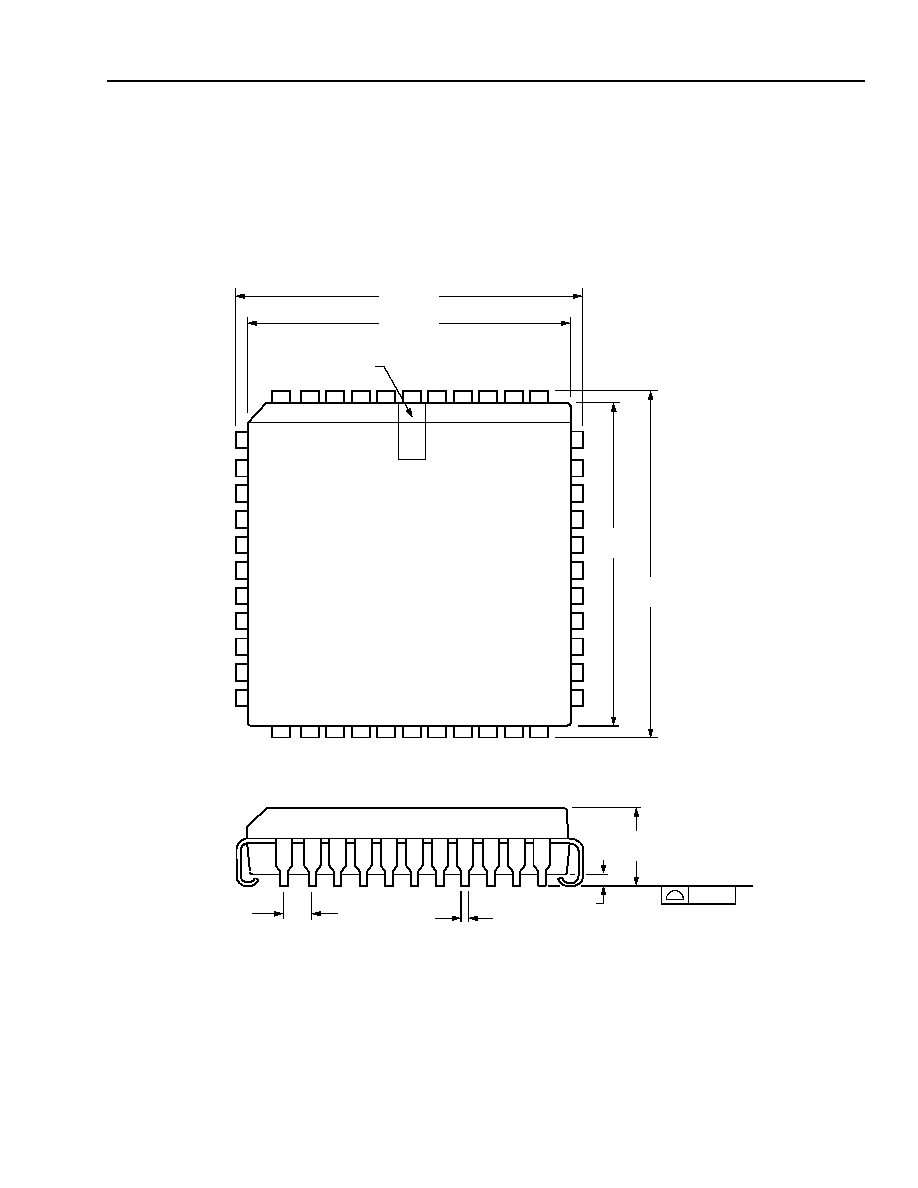
44-Pin PLCC
Dimensions are in millimeters.
Note: The dimensions in this outline diagram are intended for informational purposes only. For detailed schemat-
ics to assist your design efforts, please contact your Agere Communications Sales Representative.
5-2506(F)r7
4.57
MAX
1.27 TYP
0.53
MAX
0.10
SEATING PLANE
0.51 MIN
TYP
1
6
40
7
17
29
39
18
28
PIN #1 IDENTIFIER
ZONE
16.66 MAX
17.65 MAX
16.66
MAX
17.65
MAX

Data Sheet
September 2001
L7585F Full-Feature, Low-Power SLIC and Switch
Agere Systems Inc. reserves the right to make changes to the product(s) or information contained herein without notice. No liab ility is assumed as a result of their use or application.
Copyright © 2001 Agere Systems Inc.
All Rights Reserved
September 2001
DS01-312ALC (Replaces DS00-216ALC)
For additional information, contact your Agere Systems Account Manager or the following:
INTERNET:
http://www.agere.com
E-MAIL:
docmaster@agere.com
N. AMERICA:
Agere Systems Inc., 555 Union Boulevard, Room 30L-15P-BA, Allentown, PA 18109-3286
1-800-372-2447, FAX 610-712-4106 (In CANADA: 1-800-553-2448, FAX 610-712-4106)
ASIA:
Agere Systems Hong Kong Ltd., Suites 3201 & 3210-12, 32/F, Tower 2, The Gateway, Harbour City, Kowloon
Tel. (852) 3129-2000, FAX (852) 3129-2020
CHINA: (86) 21-5047-1212 (Shanghai), (86) 10-6522-5566 (Beijing), (86) 755-695-7224 (Shenzhen)
JAPAN: (81) 3-5421-1600 (Tokyo), KOREA: (82) 2-767-1850 (Seoul), SINGAPORE: (65) 778-8833, TAIWAN: (886) 2-2725-5858 (Taipei)
EUROPE:
Tel. (44) 7000 624624, FAX (44) 1344 488 045
Ordering Information
IEEE
is a registered trademark of The Institute of Electrical and Electronics Engineers, Inc.
MMC
is a trademark of Microelectronic Modules Corporation.
Device Part No.
Description
Package
Comcode
LUCL7585FP-D
Full-Feature, Low-Power
SLIC and Switch
44-Pin PLCC (Dry Bag)
108417023
LUCL7585FP-DT
Full-Feature, Low-Power
SLIC and Switch
44-Pin PLCC (Tape and Reel, Dry Bag)
108417031


