
Data Sheet
April 2000
L8560 Low-Power SLIC with Ringing
Features
s
Full-feature set for central office applications
s
Also ideal for ISDN terminal adapters, pair gain,
and cable telephony applications
s
Auxiliary input for second battery, and internal
switch to enable its use to save power in short tele-
phone loops
s
5 V only operation or optional ±5 V operation for
reduced power consumption
s
Low active power (85 mW typical) and scan power
(61 mW typical) with 5 V only operation
s
Low active power (68 mW typical with auxiliary bat-
tery) and scan power (45 mW typical) with ±5 V
operation
s
Quiet tip/ring polarity reversal
s
Per-line ringing available for short loops
s
Reduced overhead and increased current limit dur-
ing ring mode for lower-battery operation or
increased ring loop length
s
Supports meter pulse injection
s
Distortion-free full duplex from 0 mA dc loop cur-
rent on-hook transmission
s
Convenient operating states:
-- Forward powerup
-- Polarity reversal powerup
-- Forward sleep
-- Ground start
-- Disconnect
s
Adjustable supervision functions:
-- Off-hook detector with longitudinal rejection
-- Ground key detector with longitudinal rejection
-- Ring trip detector
s
Independent, adjustable dc and ac parameters:
-- dc feed resistance (44-pin PLCC version)
-- Loop current limit
-- Termination impedance
s
Thermal protection
Description
The L8560 full-feature, low-power subscriber line
interface circuit (SLIC) is optimized for low power
consumption while providing an extensive set of fea-
tures. This part is ideal for ISDN terminal adapter
applications and short-loop, power-sensitive applica-
tions such as pair gain and cable telephony. This part
is also designed for PBX, DLC, or CO applications.
The SLIC includes an auxiliary battery input and a
battery switch. In short-loop applications, SLICs can
be used in high battery to present a high on-hook
voltage, and then switched to low battery to reduce
off-hook power.
To help minimize the required auxiliary battery volt-
age, the dc feed resistance and overhead voltage are
set at 55
and 6.7 V, respectively. This allows an
undistorted on-hook transmission of a 3.14 dBm sig-
nal into a 900
loop impedance.
The device offers the reverse battery function. Using
the reverse battery, the device can provide a bal-
anced power ring signal to tip and ring. In this
mode of operation, the battery switch is used to
apply a high-voltage battery during ringing and a
lower-voltage battery during the talk and idle states.
Also included in the L8560 is a dc current-limit
switch, which increases the dc current limit during
power ringing. In addition, dc overhead voltage is
reduced during the ring state. With the battery and
current-limit switches, and overhead reduction, the
L8560 can provide sufficient power to ring a true
North American 5 REN load of 1386
+ 40
µ
F.
The device offers ring trip and loop closure supervi-
sion with 0.3 V and 2 mA hysteresis, respectively. It
also includes the ground start state and ring ground
detection. A summing node for meter pulse injection
to 2.2 Vrms is also included. The 44-pin PLCC ver-
sion also has a spare uncommitted op amp, which
may be used for ac gain setting or meter pulse filter-
ing.

Data Sheet
April 2000
L8560 Low-Power SLIC with Ringing
2
Lucent Technologies Inc.
Table of Contents
Contents
Page
Features .................................................................... 1
Description ................................................................. 1
Pin Information ........................................................... 6
Functional Description ................................................ 9
Absolute Maximum Ratings ..................................... 10
Recommended Operating Conditions ...................... 11
Electrical Characteristics .......................................... 11
Ring Trip Requirements ......................................... 16
Test Configurations .................................................. 17
Applications ............................................................. 19
Characteristic Curves............................................. 19
dc Applications ...................................................... 21
Battery Feed...................................................... 21
Overhead Voltage ............................................ 22
Adjusting Overhead Voltage ............................. 23
Adjusting dc Feed Resistance........................... 23
Adjusting Overhead Voltage and dc Feed
Resistance Simultaneously.............................. 24
Loop Range....................................................... 24
Off-Hook Detection ........................................... 24
Ring Ground Detection...................................... 25
Longitudinal Balance.............................................. 25
Power Derating ..................................................... 25
Battery Switch ....................................................... 26
V
CC
/V
EE
Supplies ................................................... 27
Power Ringing ....................................................... 27
Ringing SLIC Balanced Ring Signal
Generation ....................................................... 27
POTS for ISDN Terminal Adapters ................... 27
Contents
Page
Power Ringing Load .......................................... 28
Crest Factor....................................................... 28
Current-Limit Switch .......................................... 29
Ring Trip ............................................................ 29
Reference Designs for ISDN TA Applications ... 31
Design Considerations .......................................... 33
Unbalanced Bused Ring Signal Application ...... 33
Ring Trip Detection............................................ 33
ac Design .............................................................. 37
First-Generation Codecs ................................... 37
Second-Generation Codecs .............................. 37
Third-Generation Codecs .................................. 37
Design Examples ................................................... 39
Example 1, Real Termination ............................ 39
Example 2, Complex Termination ..................... 39
Example 3, Complex Termination Without
Spare Op Amp ................................................. 39
Complex Termination Impedance Design
Example Using L8560 Without Spare
Op Amp ............................................................ 40
ac Interface Using First-Generation Codec ....... 40
Transmit Gain .................................................... 41
Receive Gain ..................................................... 42
Hybrid Balance .................................................. 42
Blocking Capacitors........................................... 43
Outline Diagrams...................................................... 44
32-Pin PLCC ......................................................... 44
44-Pin PLCC ......................................................... 45
Ordering Information................................................. 46

Data Sheet
April 2000
Lucent Technologies Inc.
3
L8560 Low-Power SLIC with Ringing
Table of Contents
(continued)
Figures
Page
Figure 1. Functional Diagram ..................................... 5
Figure 2. 32-Pin Diagram (PLCC Chip) ...................... 6
Figure 3. 44-Pin Diagram (PLCC Chip) ...................... 6
Figure 4. Ring Trip Circuits....................................... 16
Figure 5. Basic Test Circuit ...................................... 17
Figure 6. Metallic PSRR ........................................... 17
Figure 7. Longitudinal PSRR .................................... 17
Figure 8. Longitudinal Balance ................................. 18
Figure 9. RFI Rejection............................................. 18
Figure 10. Longitudinal Impedance .......................... 18
Figure 11. ac Gains .................................................. 18
Figure 12. L8560 Receive Gain and Hybrid
Balance vs. Frequency .......................... 19
Figure 13. L8560 Transmit Gain and Return Loss
vs. Frequency ........................................ 19
Figure 14. L8560 Typical V
CC
Power Supply
Rejection ................................................ 19
Figure 15. L8560 Typical V
BAT
Power Supply
Rejection ................................................ 19
Figure 16. Loop Closure Program Resistor
Selection ................................................ 20
Figure 17. Ring Ground Detection Programming ..... 20
Figure 18. Loop Current vs. Loop Voltage................ 20
Figure 19. Loop Current vs. Loop Resistance .......... 20
Figure 20. L8560 Typical SLIC Power Dissipation
vs. Loop Resistance............................... 21
Figure 21. Power Derating........................................ 21
Figure 22. Loop Current vs. Loop Voltage................ 21
Figure 23. SLIC 2-Wire Output Stage ....................... 23
Figure 24. Equivalent Circuit for Adjusting the
Overhead Voltage .................................. 23
Figure 25. Equivalent Circuit for Adjusting the
dc Feed Resistance ............................... 23
Figure 26. Adjusting Both Overhead Voltage and
dc Feed Resistance ............................... 24
Figure 27. Off-Hook Detection Circuit....................... 24
Figure 28. POTS Controlled from an ISDN
Terminal Adapter ................................... 28
Figure 29. Ringing Waveform Crest Factor = 1.6 ..... 28
Figure 30. Ringing Waveform Crest Factor = 1.2 ..... 28
Figure 31. Equivalent Ring Trip Circuit for
Balanced Ringing SLIC ......................... 29
Figure 32. Thevenin Equivalent Ring Trip Circuit
for Balanced Ringing SLIC..................... 29
Figure 33. POTS Interface with Balanced Ringing
Using L8560 SLIC and T8503 Codec .... 31
Figure 34. Ring Trip Equivalent Circuit and
Equivalent Application ........................... 33
Figure 35. Basic Loop Start Application Circuit
Using T7504 Codec and Bused
Ringing ................................................... 34
Figure 36. Ground Start Application Circuit .............. 35
Figure 37. ac Equivalent Circuit Not Including
Spare Op Amp ....................................... 38
Figure 38. ac Equivalent Circuit Including Spare
Op Amp .................................................. 38
Figure 39. Interface Circuit Using First-Generation
Codec (Blocking Capacitors Not
Shown) ................................................... 41
Figure 40. ac Interface Using First-Generation
Codec (Including Blocking Capacitors)
for Complex Termination Impedance ..... 43
Tables
Page
Table 1. L8560 Product Family Feature Summary ..... 4
Table 2. Pin Descriptions............................................ 7
Table 3. Input State Coding ........................................ 9
Table 4. Supervision Coding ...................................... 9
Table 5. Power Supply ............................................. 12
Table 6. 2-Wire Port ................................................. 13
Table 7. Analog Pin Characteristics ......................... 14
Table 8. Uncommitted Op Amp
Characteristics (44-Pin PLCC Only).......... 14
Table 9. ac Feed Characteristics .............................. 15
Table 10. Logic Inputs and Outputs.......................... 16
Table 11. Parts List for Balanced Ringing Using
T8503 Codec .......................................... 32
Table 12. Parts List for Loop Start with Bused
Ringing and Ground Start Applications .. 35
Table 13. 600
Design Parameters ........................ 37

Data Sheet
April 2000
L8560 Low-Power SLIC with Ringing
4
Lucent Technologies Inc.
Description
(continued)
The L8560 product family is graded by different fea-
tures, specifications, and package options. The
L8560Axx is the basic full-feature SLIC that operates
with 5 V and a battery supply, and is available in the
32-pin PLCC (AAU) package and the 44-pin PLCC
package (AP). This part is graded as the 54 dB longitu-
dinal balance part. Additional features (spare op amp
and overhead voltage programming) are available in
the 44-pin PLCC package.
The L8560CAU is available only in the 32-pin PLCC
package and has a feature set similar to the AAU ver-
sion, except the CAU version requires +5 V, ≠5 V, and
battery power supplies. With this option, power con-
sumption is greatly reduced.
The L8560DAU and L8560EP are available in the
32-pin and 44-pin PLCC packages and have feature
sets identical to the L8560AAU and L8560AP, respec-
tively, with the following modifications. These parts are
graded as high longitudinal balance (63 dB), and have
an additional logic state (scan with low battery) which
allows for low on-hook power dissipation.
The L8560FAU and L8560GP are available in the
32-pin and 44-pin PLCC packages and have feature
sets identical to the L8560AAU and L8560AP, respec-
tively, with the following modifications. These parts are
graded for lower longitudinal balance (50 dB), and
have an additional logic state (scan with battery) which
allows for low on-hook power dissipation.
Table 1 below summarizes the features in the L8560
product family.
Table 1. L8560 Product Family Feature Summary
* More information is provided in the Applications section of this document.
Feature
L8560
AAU
AP
CAU
DAU
EP
FAU
GP
32-Pin PLCC
X
NA
X
X
NA
X
NA
44-Pin PLCC
NA
X
NA
NA
X
NA
X
5 V Operation
X
X
NA
X
X
X
X
±5 V Operation (reduced power consumption)
NA
NA
X
NA
NA
NA
NA
Operational V
BAT1
(V)
≠70
≠70
≠70
≠70
≠70
≠70
≠70
Battery Switch
X
X
X
X
X
X
X
Balanced Ring Mode
X
X
X
X
X
X
X
Adjustable Overhead
NA
X
NA
NA
X
NA
X
Spare Op Amp
NA
X
NA
NA
X
NA
X
Reverse Battery
X
X
X
X
X
X
X
Scan Mode
X
X
X
X
X
X
X
Scan Mode with Low Battery
NA
NA
NA
X
X
X
X
Longitudinal Balance (dB)*
54
54
54
63
63
50
50
On-hook Transmission
X
X
X
X
X
X
X
Ground Start
X
X
X
X
X
X
X
Loop Start
X
X
X
X
X
X
X
Ring Trip Detector
X
X
X
X
X
X
X
Programmable Current Limit
X
X
X
X
X
X
X
Thermal Protection
X
X
X
X
X
X
X
Lucent Technologies Inc.
5
Data Sheet
April 2000
L8560 Low-Power SLIC with Ringing
Description
(continued)
12-2569.c (F)
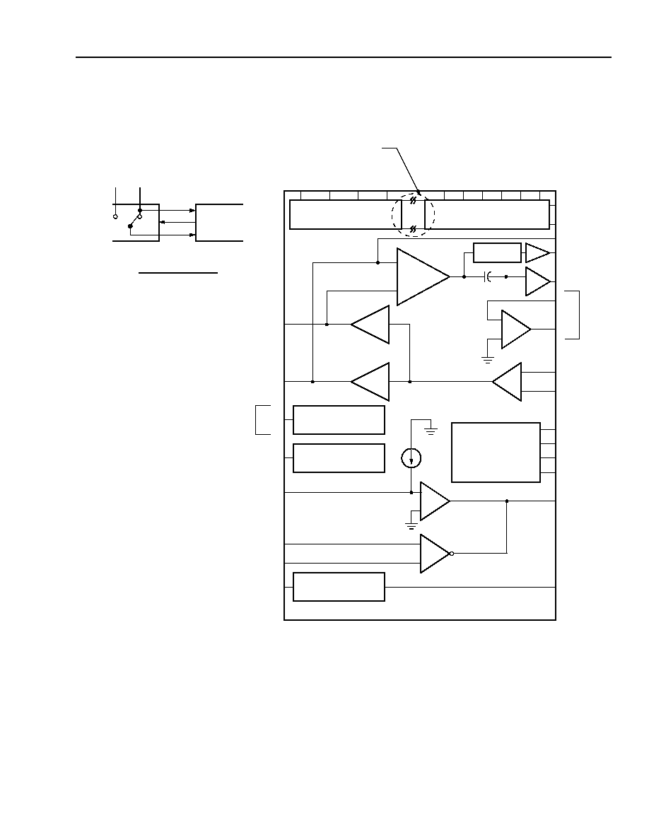
Figure 1. Functional Diagram
RGDET
ICM
B0
B1
B2
BR
+
≠
+
≠
AX
A = 4
A = ≠4
POWER CONDITIONING
BG
ND
BS
1
BS
2
V
CC
AG
ND
PT
PR
dc RESISTANCE
ADJUST
DCR
RTSN
RTSP
LCTH
RING TRIP DETECTOR
LOOP CLOSURE DETECTOR
BATTERY FEED
SPARE
DCOUT
VITR
RCVP
RCVN
XMT
SN
NSTAT
1
V
TX
T
XI
0.1
µ
F
2
RECTIFIER
CF2
CF1
BATTERY SWITCH
FB
1
FB
2
TG
RING GROUND
DETECTOR
44-PIN
PLCC
ONLY
CURRENT-LIMIT
ADJUST
I
PROG
44-PIN
V
BAT
1
V
BAT
2
INTERNAL SWITCH
V
REG
V
EE
(O
PT
IO
NA
L
BATTERY
ENLARGED DETAIL
V
BAT
2
V
BAT
1
V
BAT1
DECISION
SWITCH
SEE ENLARGED DETAIL
& REFERENCE
ON L8560
C)
19.2
C
EXTERNAL
OP AMP
+
≠
STATE CONTROL
+
≠
+
≠
PLCC
ONLY
Data Sheet
April 2000
L8560 Low-Power SLIC with Ringing
6
Lucent Technologies Inc.
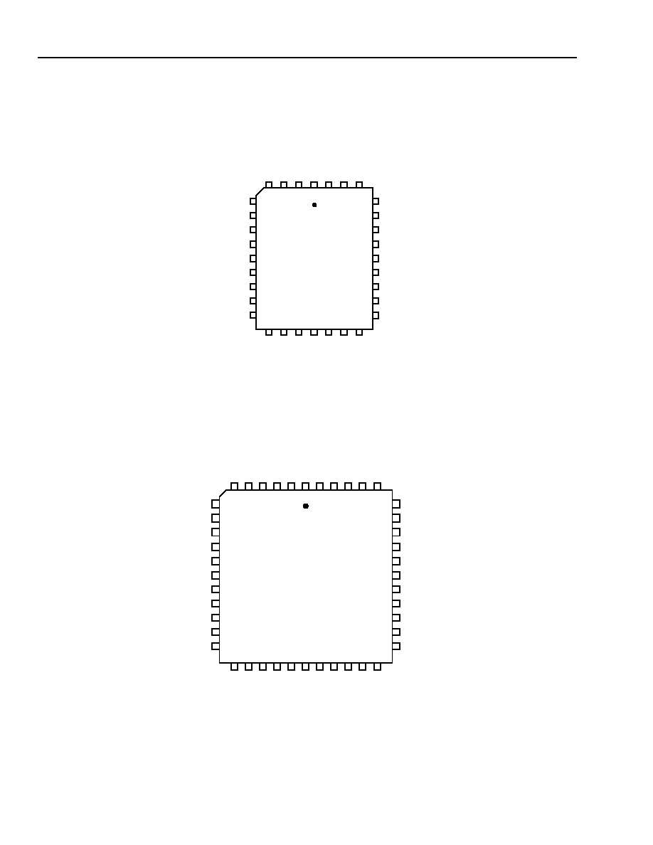
Pin Information
12-2548.L (F)
Figure 2. 32-Pin Diagram (PLCC Chip)
12-2548.f (F)
Figure 3. 44-Pin Diagram (PLCC Chip)
B0
BR
B2
PR
PT
BS1
BS2
ICM
B1
5
7
8
9
10
11
12
13
14 15
6
4
3
2
1
32
30
16
18 19 20
17
31
27
26
25
24
23
22
21
28
29
FB1
FB2
RCVN
LCTH
I
PROG
DCOUT
CF2
CF1
RTSN
RCV
P
TX
I
VT
X
TG
32-PIN PLCC
RG
D
E
T
BGN
D
RTSP
V
ITR
AGN
D
NS
T
A
T
V
BAT
2
V
BAT
1
NC (L8560A
/
D
/F
)
V
EE
(L8560C)
V
CC
7
9
10
11
12
13
14
15
16
17
8
6
4
3
2
1 44 43 42 41 40
5
18
20 21 22 23 24 25 26
DCOUT
NC
27 28
19
39
37
36
35
34
33
32
31
30
29
38
RCVP
NC
VITR
TXI
VTX
TG
NC
NC-NTP
AGND
NC
RTSP
V
BAT1
BGND
RGDET
CF2
BS
2
B0
B1
B2
NC
PR
NC
BS
1
PT
NC
FB
2
FB
1
LCTH
DCR
CF1
SN
NC
XM
T
BR
RCVN
NSTAT
NC
ICM
RTSN
44-PIN PLCC
I
PR
O
G
V
BAT2
V
CC

Lucent Technologies Inc.
7
Data Sheet
April 2000
L8560 Low-Power SLIC with Ringing
Pin Information
(continued)
Table 2. Pin Descriptions
32-Pin 44-Pin Symbol Type
Description
9
1
DCOUT
O
dc Output Voltage. This output is a voltage that is directly proportional to the
absolute value of the differential tip/ring current.
10
2
I
PROG
I
Current-Limit Program Input. A resistor to DCOUT sets the dc current limit of
the device.
11
3
CF2
--
Filter Capacitor 2. Connect a 0.1
µ
F capacitor from this pin to AGND.
12
4
CF1
--
Filter Capacitor 1. Connect a 0.47
µ
F capacitor from this pin to pin CF2.
--
5
SN
I
Summing Node. The inverting input of the uncommitted operational amplifier.
A resistor or network to XMT sets the gain (44-pin PLCC only).
--
6
XMT
O
Transmit ac Output Voltage. The output of the uncommitted operational
amplifier (44-pin PLCC only).
13
7
RTSN
I
Ring Trip Sense Negative. Connect this pin to the ringing generator signal
through a high-value resistor.
14
8
RTSP
I
Ring Trip Sense Positive. Connect this pin to the ring relay and the ringer
series resistor through a high-value resistor.
--
9
NC
--
No Connection. May be used as a tie point.
15
10
AGND
--
Analog Signal Ground.
--
11
NC
--
No Connection. May be used as a tie point.
16
12
V
CC
--
5 V Power Supply.
17
13
V
BAT1
--
Battery Supply. Negative high-voltage battery, higher in magnitude than V
BAT2
.
18
14
V
BAT2
--
Auxiliary Battery Supply. Negative high-voltage battery, lower in magnitude
than V
BAT1
, used to reduce power dissipation on short loops.
19
15
BGND
--
Battery Ground. Ground return for the battery supply.
20
16
RGDET
O
Ring Ground Detect. When high, this open-collector output indicates the pres-
ence of a ring ground. To use, connect a 100 k
resistor to V
CC
.
21
17
ICM
I
Common-Mode Current Sense. To program ring ground sense threshold,
connect a resistor to V
CC
and connect a capacitor to AGND to filter 50/60 Hz. If
unused, the pin should be connected to ground.
22
18
BS2
--
Battery Switch Slowdown. Connect a 0.22
µ
F capacitor to pin BS1.
23
19
BS1
--
Battery Switch Slowdown. Connect a 0.22
µ
F capacitor to pin BS2. Also, con-
nect a 0.1 µF capacitor in series with a 100
resistor from BS1 to V
BAT1
for sta-
bility.
--
20
NC
--
No Connection. May be used as a tie point.
--
21
NC
--
No Connection. May be used as a tie point.
24
22
PT
I/O
Protected Tip. The output of the tip driver amplifier and input to loop sensing.
Connect to loop through overvoltage protection.
25
23
PR
I/O
Protected Ring. The output of the ring driver amplifier and input to loop sens-
ing circuitry. Connect to loop through overvoltage protection.

Data Sheet
April 2000
L8560 Low-Power SLIC with Ringing
8
Lucent Technologies Inc.
Pin Information
(continued)
Table 2. Pin Descriptions
(continued)
32-Pin 44-Pin
Symbol
Type
Description
--
24
NC
--
No Connection. May be used as a tie point.
26
25
B2
I
State Control Input. B0, B1, B2, and BR determine the state of the SLIC.
See Table 3. Pin B2 has a 40 k
pull-up.
27
26
B1
I
State Control Input. B0, B1, B2, and BR determine the state of the SLIC.
See Table 3. Pin B1 has a 40 k
pull-up.
28
27
B0
I
State Control Input. B0, B1, B2, and BR determine the state of the SLIC.
See Table 3. Pin B0 has a 40 k
pull-up.
29
28
BR
I
State Control Input. B0, B1, B2, and BR determine the state of the SLIC.
See Table 3. Pin BR has a 40 k
pull-up.
--
29
NC
--
No Connection. May be used as a tie point.
--
30
NC-NTP
--
No Connection. May not be used as a tie point.
--
31
NC
--
No Connection. May be used as a tie point.
30
32
TG
--
Transmit Gain. Connect a 4.32 k
resistor from this pin to VTX.
31
33
VTX
O
The voltage at this pin is directly proportional to the differential tip/ring current.
32
34
TXI
--
ac/dc Separation. Connect a 0.1
µ
F capacitor from this pin to VTX.
1
35
NSTAT
O
Loop Detector Output/Ring Trip Detector Output. This output is a wired-
OR of the NLC/NRDET outputs. When low, this logic output indicates that an
off-hook condition exists or that ringing has been tripped.
2
--
V
EE
--
≠5 V Power Supply L8560C.
2
--
NC
--
No Connection L8560A/D/F. May be used as a tie point.
--
36
NC
--
No Connection. May be used as a tie point.
3
37
VITR
O
ac Output Voltage. This output is a voltage that is directly proportional to the
differential ac tip/ring current.
4
38
RCVP
I
Receive ac Signal Input (Noninverting). This high-impedance input con-
trols the ac differential voltage on tip and ring.
5
39
RCVN
I
Receive ac Signal Input (Inverting). This high-impedance input controls the
ac differential voltage on tip and ring.
--
40
NC
--
No Connection. May be used as a tie point.
6
41
FB2
--
Polarity Reversal Slowdown. Connect a capacitor to ground.
7
42
FB1
--
Polarity Reversal Slowdown. Connect a capacitor to ground.
8
43
LCTH
I
Loop Closure Threshold Input. Connect a resistor to DCOUT to set off-
hook threshold.
--
44
DCR
I
dc Resistance. Short to analog ground for dc feed resistance of 55
. The dc
feed resistance can be increased to a nominal 760
by shorting DCR to
DCOUT. Intermediate values can be set by a simple resistor divider from
DCOUT to ground with the trip at DCR (44-pin PLCC only).

Lucent Technologies Inc.
9
Data Sheet
April 2000
L8560 Low-Power SLIC with Ringing
Functional Description
Table 3. Input State Coding
Table 4. Supervision Coding
B0
B1
B2
BR
State/Definition
1
1
0
1
Powerup, Forward Battery V
BAT2
. Pin PT is positive with respect to pin PR. V
BAT2
is applied
to the tip/ring drive amplifiers. On-hook transmission capability. All supervision active--an
off-hook condition or a ring trip causes output NSTAT to go low.
1
0
0
1
Powerup, Reverse Battery V
BAT2
. Pin PR is positive with respect to pin PT. V
BAT2
is applied
to the tip/ring drive amplifiers. On-hook transmission capability. All supervision active--an
off-hook condition or a ring trip causes output NSTAT to go low.
1
1
1
1
Powerup, Forward Battery V
BAT1
. Pin PT is positive with respect to pin PR. V
BAT1
is applied
to the tip/ring drive amplifiers. On-hook transmission capability. All supervision active--an
off-hook condition or a ring trip causes output NSTAT to go low.
1
0
1
1
Powerup, Reverse Battery V
BAT1
. Pin PR is positive with respect to pin PT. V
BAT1
is applied
to the tip/ring drive amplifiers. On-hook transmission capability. All supervision active--an
off-hook condition or a ring trip causes output NSTAT to go low.
0
1
1
1
Ground Start. Tip drive amplifier is turned off. The device presents a high impedance
(>100 k
) to pin PT and a current-limited battery (V
BAT1
) to pin PR. Output pin RGDET indi-
cates current flowing in the ring lead.
0
0
1
1
Low-Power Scan. Except for off-hook supervision, all circuits are shut down to conserve
power. Only the off-hook detector affects output pin NSTAT. V
BAT1
is applied to the tip/ring
drive amplifiers. Pin PT is positive with respect to pin PR. On-hook transmission is disabled.
0
1
0
1
Low-Power Scan (L8560D/E/F/G Only). Except for off-hook supervision, all circuits are shut
down to conserve power. Only the off-hook detector affects output pin NSTAT. V
BAT2
is ap-
plied to the tip/ring drive amplifiers. Pin PT is positive with respect to pin PR. On-hook trans-
mission is disabled.
0
0
0
1
Forward Disconnect. The tip and ring amplifiers are turned off and the SLIC goes into a
high-impedance state (>100 k
). V
BAT2
is applied to the SLIC.
1
1/0
1
0
Ring State. SLIC is powered up. V
BAT1
is applied to the tip and ring amplifiers. Current limit
is increased by a factor of 2.8. Overhead voltage is reduced to approximately 2.4 V. These
conditions are necessary to supply sufficient power to drive a true North American 5 REN
ringing load (1386
+ 40
µ
F). Loop closure detector is disabled--only the ring trip detector
affects output pin NSTAT. To apply a balanced ring signal to pins PR and PT, apply a 0 V to
5 V square wave to input pin B1. Ringing frequency is the frequency of the input wave at B1.
To shape the ring signal at pins PR and PT, connect a capacitor from pin FB1 to ground and
from pin FB2 to ground.
Pin NSTAT
Pin RGDET
0 = off-hook or ring trip
1 = ring ground
1 = on-hook and no ring trip
0 = no ring ground

Data Sheet
April 2000
L8560 Low-Power SLIC with Ringing
10
Lucent Technologies Inc.
Absolute Maximum Ratings
(T
A
= 25
∞
C)
Stresses in excess of the absolute maximum ratings can cause permanent damage to the device. These are abso-
lute stress ratings only. Functional operation of the device is not implied at these or any other conditions in excess
of those given in the operational sections of the data sheet. Exposure to absolute maximum ratings for extended
periods can adversely affect device reliability.
Note: The IC can be damaged unless all ground connections are applied before, and removed after, all other connections. Furthermore, when
powering the device, the user must guarantee that no external potential creates a voltage on any pin of the device that exceeds the
device ratings. Some of the known examples of conditions that cause such potentials during powerup are 1) an inductor connected to tip
and ring can force an overvoltage on V
BAT
through the protection devices if the V
BAT
connection chatters, and 2) inductance in the V
BAT
lead could resonate with the V
BAT
filter capacitor to cause a destructive overvoltage.
Parameter
Symbol
Value
Unit
5 V Power Supply
V
CC
7.0
V
≠5 V Power Supply (L8560C)
V
EE
≠7.0
V
Battery (talking) Supplies
V
BAT1,
V
BAT2
≠75
V
V
BAT2
Magnitude
IV
BAT2
I
IV
BAT1
I + 0.4
V
Logic Input Voltage
--
≠0.5 to +7.0
V
Analog Input Voltage
--
≠7.0 to +7.0
V
Maximum Junction Temperature
T
J
165
∞
C
Storage Temperature Range
T
stg
≠40 to +125
∞
C
Relative Humidity Range
R
H
5 to 95
%
Ground Potential Difference (BGND to AGND)
--
±
3
V
PT or PR Fault Voltage (dc)
V
PT
, V
PR
(V
BAT1
≠ 5) to +3
V
PT or PR Fault Voltage (10 x 1000
µ
s)
V
PT
, V
PR
(V
BAT1
≠ 15) to +15
V
Current into Ring Trip Inputs
I
RTSP
, I
RTSN
±
240
µ
A

Lucent Technologies Inc.
11
Data Sheet
April 2000
L8560 Low-Power SLIC with Ringing
Recommended Operating Conditions
Electrical Characteristics
Minimum and maximum values are testing requirements in the temperature range of 25 ∞C to 85 ∞C and battery
range of ≠24 V to ≠70 V. These minimum and maximum values are guaranteed to ≠40 ∞C based on component
simulations and design verification of samples, but devices are not tested to ≠40 ∞C in production. The test circuit
shown in Figure 5 is used, unless otherwise noted. Positive currents flow into the device.
Typical values are characteristics of the device design at 25 ∞C based on engineering evaluations and are not part
of the test requirements. Supply values used for typical characterization are V
CC
= 5.0 V, V
EE
= ≠5.0 V, V
BAT1
=
≠48 V, V
BAT2
= ≠25.5 V, unless otherwise noted.
Parameter
Min
Typ
Max
Unit
Ambient Temperature
≠40
--
85
∞
C
Loop Closure Threshold-detection Programming Range
5
10
I
LIM
mA
dc Loop Current-limit Programming Range
5
40
50
mA
On- and Off-hook 2-wire Signal Level (@ Z
LOOP
= 200
)
--
--
2.2
Vrms
ac Termination Impedance Programming Range
150
600
1300
V
BAT1
≠24
≠48
≠70
V
V
BAT2
≠16
--
V
BAT1
V
V
CC
4.5
5.0
5.5
V
V
EE
(L8560C)
≠4.75
≠5.0
≠5.5
V
dc Feed Resistance Programming Range (excl. RP)
55
55
760

Data Sheet
April 2000
L8560 Low-Power SLIC with Ringing
12
Lucent Technologies Inc.
Electrical Characteristics
(continued)
Table 5. Power Supply
V
CC
= 5.0 V, V
EE
= ≠5.0 V, V
BAT1
= ≠48 V, V
BAT2
= ≠19 V, unless otherwise noted.
1. This parameter is not tested in production. It is guaranteed by design and device characterization.
2. V
EE
used for L8560C version only.
Parameter
Min
Typ
Max
Unit
Power Supply Rejection 500 Hz to 3 kHz
(See Figures 6, 7, 14, and 15.)
1
:
V
CC
(1 kHz), V
EE
(1 kHz)
2
V
BAT1,
V
BAT2
(500 Hz--3 kHz)
35
45
--
--
--
--
dB
dB
Thermal Protection Shutdown (T
jc
)
--
165
--
∞
C
Thermal Resistance, Junction to Ambient (
JA
), Still Air, 44-pin PLCC
Thermal Resistance, Junction to Ambient (
JA
), Still Air, 32-pin PLCC
--
--
47
60
--
--
∞
C/W
∞
C/W
Power Supply--Powerup, No Loop Current, V
BAT2
Applied
L8560A/D/E/F/G:
I
CC
I
BAT1
I
BAT2
--
--
--
6.0
120
2.6
7.2
200
3.2
mA
µA
mA
Power Supply--Powerup, No Loop Current, V
BAT1
Applied:
I
CC
(L8560A/D/E/F/G)
I
BAT1
(L8560A)
I
BAT1
(L8560D/E/F/G)
I
BAT2
(L8560D/E/F/G)
--
--
--
--
6.0
2.8
1.65
1.0
7.2
3.3
2.0
1.3
mA
mA
mA
mA
Power Supply--Scan Mode, Forward Battery, No Loop Current,
V
BAT1
Applied:
I
CC
(L8560A/D/E/F/G)
I
BAT1
(L8560A)
I
BAT1
(L8560D/E/F/G)
I
BAT2
(L8560D/E/F/G)
--
--
--
--
4.0
1.3
0.5
0.9
5.2
1.6
0.75
1.2
mA
mA
mA
mA
Power Supply--Scan Mode, Forward Battery, No Loop Current,
V
BAT2
Applied:
I
CC
I
BAT1
(V
BAT1
= ≠65 V)
I
BAT2
(V
BAT2
= ≠30 V)
--
--
--
4.1
200
1.2
--
--
--
mA
µA
mA
Power Supply--Powerup, No Loop Current, L8560C Only:
I
CC
I
EE
I
BAT1
(V
BAT1
applied)
I
BAT2
(V
BAT2
applied)
I
BAT1
(V
BAT2
applied)
--
--
--
--
--
5.8
0.9
1.65
1.50
120
7.2
1.26
2.2
1.96
200
mA
mA
mA
mA
µA
Power Supply--Scan, Forward Battery, No Loop Current, V
BAT1
Applied, L8560C Only:
I
CC
I
EE
I
BAT
(V
BAT1
applied)
--
--
--
4.1
0.81
0.43
5.5
1.1
0.56
mA
mA
mA
Power Supply--Ring Mode, No Loop Current:
I
CC
I
BAT1
--
--
6.45
2.2
--
--
mA
mA

Lucent Technologies Inc.
13
Data Sheet
April 2000
L8560 Low-Power SLIC with Ringing
Electrical Characteristics
(continued)
Table 6. 2-Wire Port
1. The longitudinal current is independent of dc loop current.
2. Current-limit I
LIM
is programmed by a resistor, R
PROG
, from pin I
PROG
to DCOUT. I
LIM
is specified at the loop resistance where current limiting
begins (see Figure 22). Select R
PROG
(k
) = 0.616 x I
LIM
(mA) ≠ onset of current limit with input BR high. When input BR is low, the current
will be increased by a factor of 2.8.
3. This parameter is not tested in production. It is guaranteed by design and device characterization.
4. Specification is reduced to |V
BAT1
+ 10.5 V| minimum when V
BAT1
= ≠70 V at 85
∞
C.
5.
IEEE
is a registered trademark of The Institute of Electrical and Electronics Engineers, Inc.
6. Longitudinal balance of circuit card will depend on loop series protection resistor matching and magnitude.
7. Tested at 1000 Hz only. Full frequency specifications guaranteed by design and device characterization.
Parameter
Min
Typ
Max
Unit
Tip or Ring Drive Current = dc + Longitudinal + Signal Currents
65
--
--
mA
Signal Current
15
--
--
mArms
Longitudinal Current Capability per Wire
1
8.5
15
--
mArms
dc Loop Current Limit
2
:
Programmability Range
3
Accuracy (B0 = BR = 5 V, R
LOOP
= 100
,
V
BAT1
= ≠48 V
or V
BAT2
= ≠25.5 V active)
5
--
--
--
50
±5
mA
%
Powerup Open Loop Voltage Levels:
Differential Voltage ≠ V
BAT2
(V
BAT2
= ≠25.5 V)
Differential Voltage ≠ V
BAT1
(V
BAT1
= ≠48 V)
4
Differential Voltage ≠ V
BAT1
(ring mode)
|V
BAT2
+ 6.9|
|V
BAT1
+ 7.1|
|V
BAT1
+ 5.5|
|V
BAT2
+ 6.5|
|V
BAT1
+ 6.7|
|V
BAT1
+ 2.4|
|V
BAT2
+ 6.1|
|V
BAT1
+ 6.3|
--
V
V
V
Ground Start State:
PT Resistance
100
--
--
k
dc Feed Resistance (for I
LOOP
below current limit)
--
55
80
Loop Resistance Range (3.17 dBm overload into 600
; not in-
cluding protection):
I
LOOP
= 20 mA at V
BAT1
= ≠48 V
I
LOOP
= 20 mA at V
BAT2
= ≠24 V
1940
760
--
--
--
--
Longitudinal to Metallic Balance--
IEEE
5
Std. 455 (See Figure
8.)
6, 7
:
L8560A/C:
200 Hz to 2999 Hz Forward/Reverse Battery
3000 Hz to 3400 Hz Forward/Reverse Battery
L8560D/E:
200 Hz to 2999 Hz Forward Battery
3000 Hz to 3400 Hz Forward Battery
200 Hz to 2999 Hz Reverse Battery
3000 Hz to 3400 Hz Reverse Battery
L8560F/G:
200 Hz to 2999 Hz Forward/Reverse Battery
3000 Hz to 3400 Hz Forward/Reverse Battery
54
49
63
58
58
54
50
45
59
54
68
63
63
59
55
50
--
--
--
--
--
--
--
--
dB
dB
dB
dB
dB
dB
dB
dB
Metallic to Longitudinal Balance:
200 Hz to 4 kHz
46
--
--
dB
RFI Rejection (See Figure 9.)
3
:
0.5 Vrms, 50
Source, 30% AM Mod. 1 kHz
500 kHz to 100 MHz
--
≠55
≠45
dBV

Data Sheet
April 2000
L8560 Low-Power SLIC with Ringing
14
Lucent Technologies Inc.
Electrical Characteristics
(continued)
Table 7. Analog Pin Characteristics
1. Loop closure threshold is programmed by resistor R
LCTH
from pin LCTH to pin DCOUT.
2. Ring ground threshold is programmed by resistor R
ICM2
from pin ICM to V
CC
.
3. This parameter is not tested in production. It is guaranteed by design and device characterization.
4. I
N
is the sourcing current at RTSN. Guaranteed if I
N
is within 5
µ
A to 30
µ
A.
Table 8. Uncommitted Op Amp Characteristics (44-Pin PLCC Only)
Parameter
Min
Typ
Max
Unit
Differential PT/PR Current Sense (DCOUT):
Gain (PT/PR to DCOUT)
Offset Voltage @ I
LOOP
= 0
--
≠200
≠41.7
--
--
200
V/A
mV
Loop Closure Detector Threshold
1
:
Programming Accuracy at 10 mA
--
--
±20
%
Ring Ground Detector Threshold
2
:
R
ICM
= 83 k
Programming Accuracy
3
--
6
--
10
±25
k
%
Ring Trip Comparator:
Input Offset Voltage
3
Internal Voltage Source (L8560A/D/E/F)
Internal Voltage Source (L8560C)
Current at Input RTSP
4
--
≠8.6
≠6.1
I
N
≠ 0.5
±10
≠8.2
≠5.7
I
N
--
≠7.6
≠5.1
I
N
+ 0.5
mV
V
V
µ
A
RCVN, RCVP:
Input Bias Current
--
≠0.2
≠1
µ
A
Loop Closure Detector Hysteresis
Variation
--
--
2
15
--
--
mA
%
THD
3
at V
PT/PR
= 2.2 Vrms, V
OH
= 12 V, Z
T
= 200
--
--
≠35
dB
VITR Output Impedance
--
5
--
VITR Output Offset Voltage
--
20
--
mV
Average/dc Current to FB1 and FB2
Tested as:
(|FB1 (FB) (≠5 V)| + |FB1 (FB) (≠63 V)| + 2|FB1 (FB) (≠35 V)| +
|FB2 (FB) (≠5 V)| + |FB2 (FB) (≠63 V)| + 2|FB2 (FB) (≠35 V)| +
|FB1 (RB) (≠5 V)| + |FB1 (RB) (≠63 V)| + 2|FB1 (RB) (≠35 V)| +
|FB2 (RB) (≠5 V)| + |FB2 (RB) (≠63 V)| + 2|FB2 (RB) (≠35 V)|)/16
--
29
--
µ
A
Accuracy
--
--
±8
%
Parameter
Min
Typ
Max
Unit
Input Offset Voltage
Input Offset Current
Input Bias Current
Differential Input Resistance
--
--
--
--
±5
±10
200
1.5
--
--
--
--
mV
nA
nA
M
Output Voltage Swing (R
L
= 10 k
)
Output Resistance (A
VCL
= 1)
--
--
±3.5
2.0
--
--
Vpk
Small-signal GBW
--
700
--
kHz

Lucent Technologies Inc.
15
Data Sheet
April 2000
L8560 Low-Power SLIC with Ringing
Electrical Characteristics
(continued)
Table 9. ac Feed Characteristics
1. Set by external components. Any complex impedance R
1
+ R2 || C between 150
and 1300
can be synthesized.
2. This parameter is not tested in production. It is guaranteed by design and device characterization.
3. Return loss and transhybrid loss are functions of device gain accuracies and the external hybrid circuit. Guaranteed performance assumes
1% tolerance external components. Not tested in production.
Parameter
Min
Typ
Max
Unit
ac Termination Impedance
1
150
--
1300
Longitudinal Impedance
--
0
--
Total Harmonic Distortion--200 Hz to 4 kHz
2
:
Off-hook
On-hook
--
--
--
--
0.3
1.0
%
%
Transmit Gain, f = 1 kHz (PT/PR to VITR; see Figure 11.)
≠392
≠400
≠408
V/A
Receive + Gain, f = 1 kHz (RCVP to PT/PR)
Receive ≠ Gain, f = 1 kHz (RCVN to PT/PR)
7.76
≠7.76
8.00
≠8.00
8.24
≠8.24
--
--
Group Delay
2
:
Transmit, Powerup
Receive
--
--
1
0.5
--
--
µ
s
µ
s
Gain vs. Frequency (transmit and receive)
(600
termination; reference 1 kHz, 1 Vrms)
2
:
200 Hz to 300 Hz
300 Hz to 3.4 kHz
3.4 kHz to 16 kHz
16 kHz to 266 kHz
≠1.00
≠0.3
≠3.0
--
0.0
0.0
≠0.1
--
0.05
0.05
0.3
2.5
dB
dB
dB
dB
Gain vs. Level (transmit and receive)(reference 0 dBV)
2
:
≠55 dB to +3 dB
≠0.05
0
0.05
dB
Return Loss
2, 3
:
200 Hz to 500 Hz
500 Hz to 3400 Hz
--
--
30
36
--
--
dB
dB
2-wire Idle-channel Noise (600
termination):
Psophometric
2
C-message
3 kHz Flat
2
--
--
--
≠87
2
10
≠77
12
20
dBmp
dBrnC
dBrn
4-wire Idle-channel Noise:
Psophometric
2
C-message
3 kHz Flat
2
--
--
--
≠82
7
15
≠77
12
20
dBmp
dBrnC
dBrn
Transhybrid Loss
3
:
200 Hz to 500 Hz
500 Hz to 3400 Hz
--
--
30
36
--
--
dB
dB
Data Sheet
April 2000
L8560 Low-Power SLIC with Ringing
16
Lucent Technologies Inc.
Electrical Characteristics
(continued)
Table 10. Logic Inputs and Outputs
Parameter
Symbol
Min
Typ
Max
Unit
Input Voltages:
Low Level (permissible range)
High Level (permissible range)
V
IL
V
IH
≠0.5
2.0
0.4
2.4
0.7
V
CC
V
V
Input Currents:
Low Level (V
CC
= 5.25 V, V
I
= 0.4 V)
High Level (V
CC
= 5.25 V, V
I
= 2.4 V)
I
IL
I
IH
≠75
≠40
≠115
≠60
≠300
≠100
µ
A
µ
A
Output Voltages (open collector with internal pull-up resistor):
Low Level (V
CC
= 4.75 V, I
OL
= 360
µ
A)
High Level (V
CC
= 4.75 V, I
OH
= ≠20
µ
A)
V
OL
V
OH
0
2.4
0.2
--
0.4
V
CC
V
V
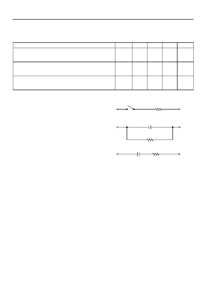
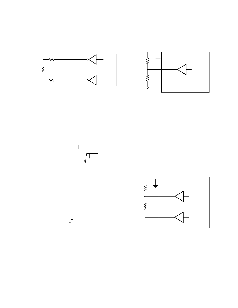
Ring Trip Requirements
s
Ringing signal:
-- Voltage, minimum 35 Vrms, maximum 100 Vrms.
-- Frequency, 17 Hz to 23 Hz.
-- Crest factor, 1.4 to 2.
s
Ringing trip:
--
100 ms (typical),
250 ms (V
BAT
= ≠33 V, loop
length = 530
).
s
Pretrip:
-- The circuits in Figure 4 will not cause ringing trip.
12-2572.e (F)
Figure 4. Ring Trip Circuits
RING
RING
RING
100
10 k
6
µ
F PER TA 909
TIP
TIP
TIP
2
µ
F
200
SWITCH CLOSES < 12 ms
8
µ
F PER TR 57
Data Sheet
April 2000
Lucent Technologies Inc.
17
L8560 Low-Power SLIC with Ringing
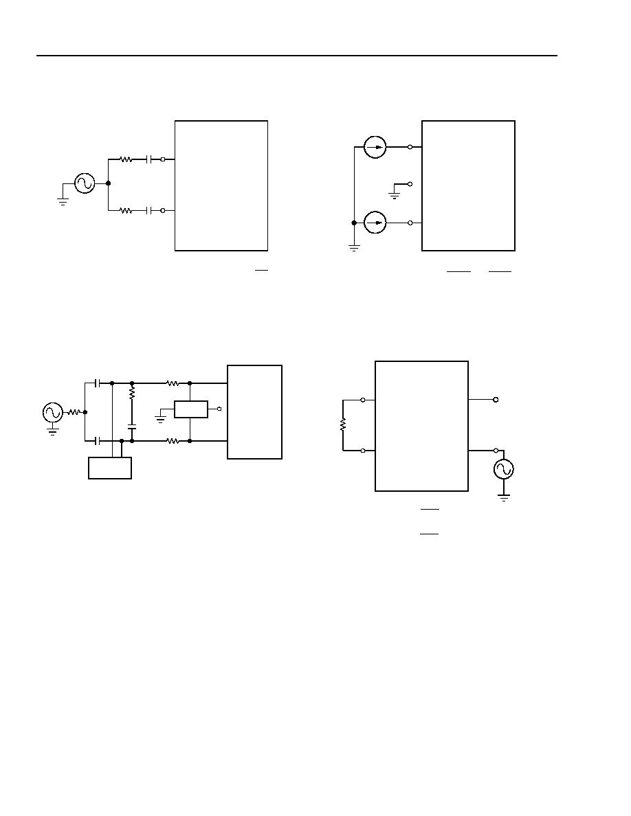
Test Configurations
12-2570.f (F)
Figure 5. Basic Test Circuit
V
CC
V
CC
AGND
0.1
µ
F
BS1
20 k
20 k
NSTAT
RGDET
XMT
66.5 k
13.7 k
RCV
30.9 k
V
BAT1
V
BAT1
BGND
PT
PR
I
PROG
DCOUT
LCTH
RTSP
RTSN
ICM
R
LOOP
23.7 k
8.25 k
100
100
V
BAT2
L8560
SLIC
VTX
TXI FB2
FB1
0.1
µ
F
BS2
B0
B2
BR
TG
V
BAT2
0.1
µ
F
B1
TIP
RING
VITR
SN
XMT
RCVN
RCVP
4.32 k
100
2 M
2 M
274 k
V
BAT
402 k
100
100
100
0.1
µ
F
VITR
RCV
30.9 k
66.5
13.7
k
k
FOR 44-PIN PLCC
FOR 32-PIN PLCC
12-2582.b (F)
Figure 6. Metallic PSRR
12-2583.b (F)
Figure 7. Longitudinal PSRR
V
S
4.7
µ
F
100
V
BAT
OR
V
CC
DISCONNECT
V
T/R
V
BAT
OR
V
CC
TIP
RING
BASIC
TEST CIRCUIT
+
≠
PSRR = 20log
V
S
V
T/R
900
BYPASS CAPACITOR
V
S
4.7
µ
F
100
V
BAT
OR
V
CC
DISCONNECT
BYPASS CAPACITOR
56.3
V
BAT
OR V
CC
TIP
RING
BASIC
TEST CIRCUIT
PSRR = 20log
V
S
V
M
67.5
10
µ
F
10
µ
F
67.5
V
M
+
≠
Data Sheet
April 2000
L8560 Low-Power SLIC with Ringing
18
Lucent Technologies Inc.
Test Configurations
(continued)
12-2584.c (F)
Figure 8. Longitudinal Balance
5-6756.a (F)
*
HP
is a registered trademark of Hewlett-Packard Company.
Notes:
V
S
= 0.5 Vrms 30% AM 1 kHz modulation.
f = 500 kHz--1 MHz.
Device in powerup mode 600
termination.
Figure 9. RFI Rejection
12-2585.a (F)
Figure 10. Longitudinal Impedance
12-2587.d (F)
Figure 11. ac Gains
TIP
RING
BASIC
TEST CIRCUIT
LONGITUDINAL BALANCE = 20 log
V
S
V
M
368
100
µ
F
100
µ
F
368
V
M
+
≠
V
S
BASIC TEST
CIRCUIT
TIP
RING
V
BAT
0.01
µ
F
0.01
µ
F
600
2.15
µ
F
82.5
82.5
HP
* 4935A
TIMS
50
1
2
4
6, 7
L7590
V
S
TIP
RING
BASIC
TEST CIRCUIT
+
≠
+
≠
I
LONG
I
LONG
V
PT
V
PR
Z
LONG
=
OR
V
PT
I
LONG
V
PR
I
LONG
TIP
RING
BASIC
TEST CIRCUIT
600
V
T/R
+
≠
G
XMT
=
V
XMT
V
T/R
G
RCV
=
V
T/R
V
RCV
XMT (44-PIN PLCC)
RCV
V
S
VITR (32-PIN PLCC)
Data Sheet
April 2000
Lucent Technologies Inc.
19
L8560 Low-Power SLIC with Ringing
Applications
Characteristic Curves
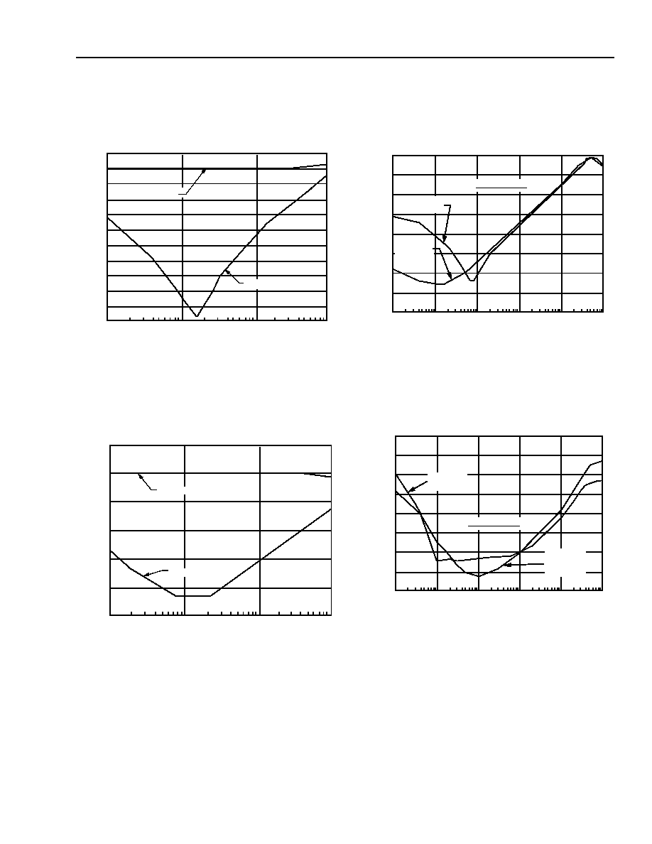
12-2828.c (F)
Figure 12. L8560 Receive Gain and Hybrid Balance
vs. Frequency
12-2829.b (F)
Figure 13. L8560 Transmit Gain and Return Loss
vs. Frequency
12-2830.a (F)
Figure 14. L8560 Typical V
CC
Power Supply
Rejection
12-2871.a (F)
Figure 15. L8560 Typical V
BAT
Power Supply
Rejection
FREQUENCY (Hz)
100
≠20
≠10
0
10
4
≠50
≠40
≠30
1000
HYBRID BALANCE
(dB
)
RECEIVE GAIN
10
5
100
1000
10
4
≠50
≠30
≠20
≠10
0
FREQUENCY (Hz)
≠40
TRANSMIT GAIN
RETURN LOSS
(d
B)
10
5
10
100
10
6
≠80
≠70
≠20
≠10
0
FREQUENCY (Hz)
1000
≠50
≠40
≠60
≠30
P
S
RR (dB)
CURRENT
LIMIT
BELOW
CURRENT
LIMIT
10
5
10
4
SPEC. RANGE
10
100
10
5
10
6
≠80
≠70
≠20
≠10
0
FREQUENCY (Hz)
1000
10
4
≠50
≠40
≠60
≠30
PS
R
R
(d
B
)
BELOW
CURRENT
LIMIT
CURRENT
LIMIT
SPEC. RANGE
Data Sheet
April 2000
L8560 Low-Power SLIC with Ringing
20
Lucent Technologies Inc.
Applications
(continued)
Characteristic Curves
(continued)
12-3015 (F)
Note: V
BAT1
= ≠48 V, I
TR
= 1.2 x 10
≠3
R
LCTH
(k
).
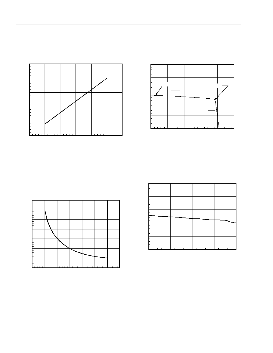
Figure 16. Loop Closure Program Resistor
Selection
12-3016.f (F)
Note: Tip lead is open; V
BAT1
= ≠48 V.
Figure 17. Ring Ground Detection Programming
12-3050.k (F)
Note: V
BAT1
= ≠48 V; I
LIM
= 22 mA; R
dc1
= 55
.
Figure 18. Loop Current vs. Loop Voltage
12-3051 (F)
Note: V
BAT1
= ≠48 V; I
LIM
= 22 mA; R
dc1
= 55
.
Figure 19. Loop Current vs. Loop Resistance
0
5
20
25
0
10
20
30
60
LOOP CLOSURE THRESHOLD RESISTOR, R
LCTH
(k
)
50
15
10
40
OFF
-H
O
O
K
THRE
SHOLD
LOO
P
CU
RRENT
(m
A)
0
5
20
35
0
20
40
60
140
100
15
10
80
25
30
120
RING GROUND CURRENT
DETECTION RESISTOR, R
ICM
(k
)
THRE
SHOLD RI
NG GROUND
C
URRENT (mA
)
0
10
20
50
0
20
30
40
50
LOOP VOLTAGE (V)
30
40
10
LOOP CURRE
NT
(m
A)
1
12.5 k
≠1
R
dc1
I
LIM
TESTED
I
LIM
ONSET
LOOP RESISTANCE, R
LOOP
(
)
0
500
1000
2000
0
20
30
40
50
1500
10
LO
OP
CUR
RENT (
m
A
)
Lucent Technologies Inc.
21
Data Sheet
April 2000
L8560 Low-Power SLIC with Ringing
Applications
(continued)
Characteristic Curves
(continued)
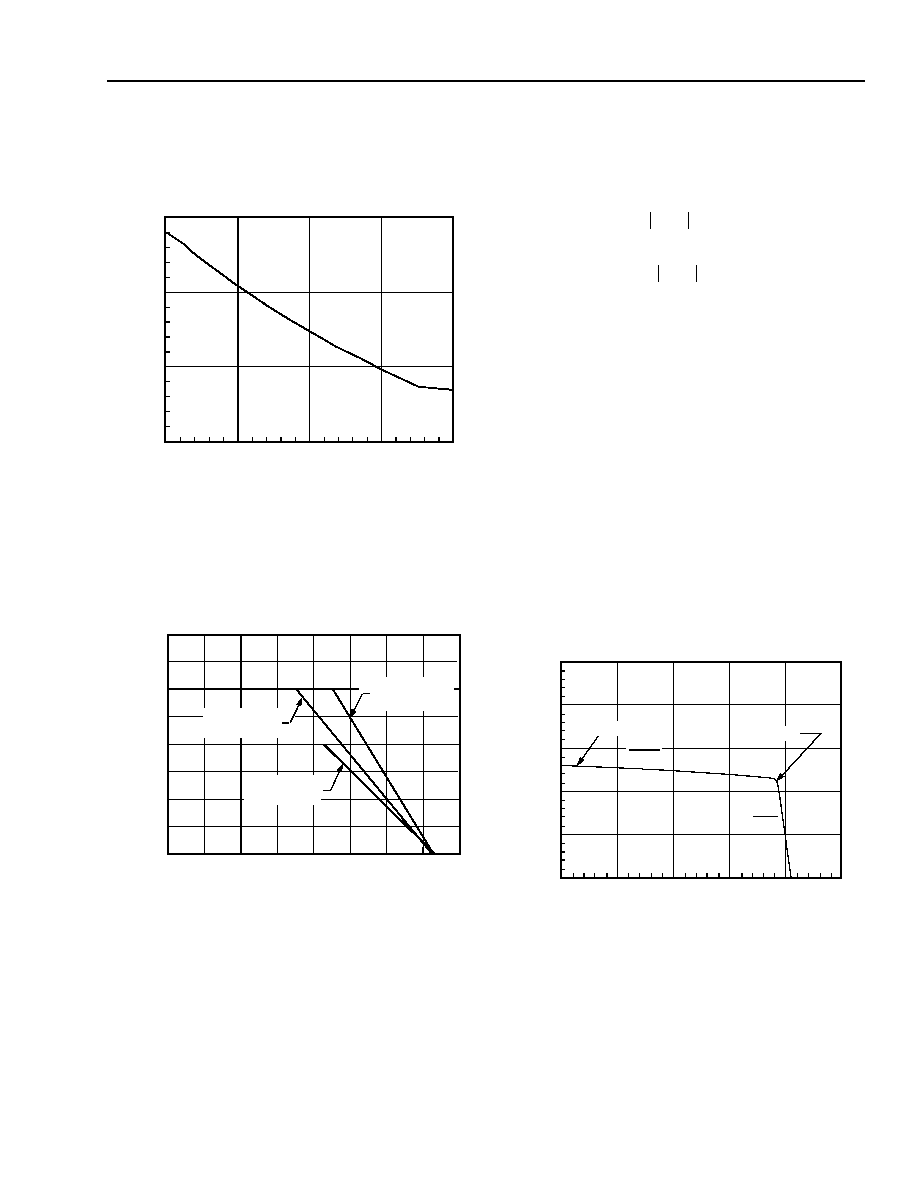
12-3052 (F)
Note: V
BAT1
= ≠48 V; I
LIM
= 22 mA; R
dc1
= 55
.
Figure 20. L8560 Typical SLIC Power Dissipation
vs. Loop Resistance
12-2825.e (F)
Figure 21. Power Derating
dc Applications
Battery Feed
The dc feed characteristic can be described by:
where:
I
L
= dc loop current.
V
T/R
= dc loop voltage.
|V
BAT
| = battery voltage magnitude.
Note: The L8560 has a battery switch circuit that
allows use of a primary battery, V
BAT1
, or an aux-
iliary battery, V
BAT2
. |V
BAT
| is the battery, V
BAT1
or
V
BAT2
, that is active. See the Battery Switch sec-
tion for more information.
V
OH
= overhead voltage. This is the difference between
the battery voltage and the open loop tip/ring
voltage.
R
L
= loop resistance, not including protection resistors.
R
P
= protection resistor value.
R
dc
= SLIC internal dc feed resistance.
The design begins by drawing the desired dc template.
An example is shown in Figure 22.
12-3050.k (F)
Note: V
BAT1
= ≠48 V; I
LIM
= 22 mA; R
dc1
= 55
.
Figure 22. Loop Current vs. Loop Voltage
LOOP RESISTANCE, R
LOOP
(
)
0
500
1000
2000
0
1000
1500
1500
500
S
L
I
C
P
O
W
E
R DISS
I
P
ATIO
N
(m
W
)
AMBIENT TEMPERATURE, T
A
(
∞
C)
20
40
60
140
180
0
500
1000
1500
2000
80
100
120
160
PO
W
E
R
(m
W
)
STILL AIR
300 cu. ft./min.
44-PIN PLCC
32-PIN PLCC
STILL AIR
44-PIN PLCC
250
750
1250
1750
I
L
V
B A T
V
O H
≠
R
L
2R
P
R
d c
+
+
----------------------------------
=
V
T/R
V
B AT
V
O H
≠
(
)
R
L
◊
R
L
2R
P
R
d c
+
+
--------------------------------------------
=
0
10
20
50
0
20
30
40
50
LOOP VOLTAGE (V)
30
40
10
LOOP CURRE
NT
(m
A)
1
12.5 k
≠1
R
dc1
I
LIM
TESTED
I
LIM
ONSET

22
22
Lucent Technologies Inc.
Data Sheet
April 2000
L8560 Low-Power SLIC with Ringing
Applications
(continued)
dc Applications
(continued)
Starting from the on-hook condition and going through
to a short circuit, the curve passes through two regions:
Region 1: On-hook and low loop currents. In this region,
the slope corresponds to the dc resistance of the SLIC,
R
dc1
(default is 55
typical). The open circuit voltage
is the battery voltage less the overhead voltage of the
device, V
OH
(default is 6.7 V typical). These values are
suitable for most applications but can be adjusted if
needed. For more information, see the sections titled
Adjusting dc Feed Resistance or Adjusting Overhead
Voltage.
Region 2: Current limit. The dc current is limited to a
starting value determined by external resistor R
PROG
, an
internal current source, and the gain from tip/ring to pin
DCOUT. Current limit is set by the equation:
I
PROG
x R
PROG
= I
LIM
x B
DCOUT
Where:
I
PROG
= the current from an internal current source
R
PROG
= the external resistor used to set the current
limit
B
DCOUT
= the transconductance from tip/ring to
DCOUT, which is nominally 41.67 V/A
During nonringing modes, the internal current source is
set at 75
µ
A, thus:
I
PROG
x R
PROG
= I
LIM
x B
DCOUT
R
PROG
= I
LIM
x B
DCOUT
/I
PROG
R
PROG
(K) = I
LIM
(mA) x 0.04167 (V/mA)/75e≠3 (mA)
R
PROG
(K) = 0.556 x I
LIM
(mA)
Testing data shows that:
R
PROG
(K) = 0.616 x I
LIM
(mA)
This equation is a first-order estimation of the loop cur-
rent at current-limit range.
For more precise loop current at current-limit range, the
loop current is also determined by loop length, protec-
tion resistance, and battery voltage. It can be shown
through calculations as follows:
Current-limit onset (I
Lonset
):
I
Lonset
(mA) =
Loop resistance where current-limit onsets (R
Lonset
):
R
Lonset
(
) =
x 1000 ≠ 2R
P
≠ Rdc
Tip/ring voltage where current-limit onsets (V
T/Ronset
):
V
T/Ronset
=
Tip/ring voltage when loop resistance is R
loop
(V
T/Rloop
):
V
T/Rloop
(V) = I
loop
(mA) x R
LOOP
(
)/1000
Loop current is now given by:
I
loop
(mA) = I
Lonset
(mA) + (V
T/Ronset
≠ V
T/Rloop
)
(V)/12.5 (k
)
or
I
loop
(mA) =
Current limit is not sensitive to temperature variation.
Overhead Voltage
In order to drive an on-hook ac signal, the SLIC must set
up the tip and ring voltage to a value less than the bat-
tery voltage. The amount that the open loop voltage is
decreased relative to the battery is referred to as the
overhead voltage and is expressed as:
V
OH
=
|
V
BAT
|
≠ (V
PT
≠ V
PR
)
Without this buffer voltage, amplifier saturation will
occur and the signal will be clipped. The L8560 is auto-
matically set at the factory to allow undistorted on-hook
transmission of a 3.17 dBm signal into a 900
loop
impedance.
The drive amplifiers are capable of 4 Vrms minimum
(V
AMP
). So, the maximum signal the device can guaran-
tee is:
V
T/R
= 4 V
For applications where higher signal levels are needed,
e.g., periodic pulse metering, the 2-wire port of the
SLIC can be programmed with pin DCR (pin DCR is
not available in the 32-pin PLCC package). The first
step is to determine the amount of overhead voltage
needed. The peak voltage at output of tip and ring
amplifiers is related to the peak signal voltage by:
R
PROG
K
( )
0.616
---------------------------------
V
BAT
V
OH
≠
(
)
V
( )
I
Lonset
mA
(
)
--------------------------------------------------
V
BAT
V
OH
≠
(
)
R
Lonset
◊
R
Lonset
2R
P
Rdc
+
+
-------------------------------------------------------------------
I
Lonset
mA
(
)
V
T Ronset
/
V
( )
+
12.5 k
(
)
/
1
R
loop
( )
12500 k
(
)
/
+
------------------------------------------------------------------------------------------------------------
Z
T/R
Z
T/R
2R
P
+
---------------------------------
V
A M P
= V
T/R
1
2R
P
Z
T/R
-----------
+
Lucent Technologies Inc.
23
Data Sheet
April 2000
L8560 Low-Power SLIC with Ringing
Applications
(continued)
dc Applications
(continued)
12-2563.c (F)
Figure 23. SLIC 2-Wire Output Stage
In addition to the required peak signal level, the SLIC
needs about 2 V from each power supply to bias the
amplifier circuitry. It can be thought of as an internal
saturation voltage. Combining the saturation voltage
and the peak signal level, the required overhead can
be expressed as:
x 10
dBm/20
where V
SAT
is the combined internal saturation voltage
between the tip/ring amplifiers and V
BAT
(4.0 V typ.). R
P
(
) is the protection resistor value. Z
T/R
(
) is the ac
loop impedance.
Example 1, On-Hook Transmission of a Meter
Pulse:
Signal level: 2.2 Vrms into 200
35
protection resistors
I
LOOP
= 0 (on-hook transmission of the metering signal)
V
OH
= 4.0 +
(2.2)
= 8.2 V
Accounting for V
SAT
tolerance of 0.5 V, a nominal over-
head of 8.7 V would ensure transmission of an undis-
torted 2.2 V metering signal.
Adjusting Overhead Voltage
To adjust the open loop 2-wire voltage, pin DCR
(44-pin PLCC only) is programmed at the midpoint of a
resistive divider from ground to either ≠5 V or V
BAT
. In
the case of ≠5 V, the overhead voltage will be indepen-
dent of the battery voltage. Figure 24 shows the equiv-
alent input circuit to adjust the overhead.
12-2562.b (F)
Figure 24. Equivalent Circuit for Adjusting the
Overhead Voltage
The overhead voltage is programmed by using the fol-
lowing equation:
V
OH
= 7.1 ≠ 18.18 V
DCR
= 7.1 ≠ 18.18
Adjusting dc Feed Resistance
The dc feed resistance may be adjusted with the help
of Figure 25.
12-2560.c (F)
Figure 25. Equivalent Circuit for Adjusting the dc
Feed Resistance
R
dc
= 55
+ 705
= 55
+ 705
≠
V
T/R
[Z
T/R
]
V
AMP
+
≠
R
P
R
P
+
V
O H
V
S AT
1
2R
P
Z
T/R
-----------
+
V
T/R
+
=
V
SA T
1
2R
P
Z
T/R
-----------
+
2 Z
T/R
1000
---------------
+
=
1
2
35
◊
200
-----------------
+
2
DCR
R
1
R
2
≠5 V
5
≠
R
1
R
2
R
1
+
---------------------
◊
DCR
R
1
R
3
DCOUT
44-PIN PLCC
V
DCR
V
DCOUT
--------------------------
R
1
R
3
R
1
+
---------------------
24
24
Lucent Technologies Inc.
Data Sheet
April 2000
L8560 Low-Power SLIC with Ringing
Applications
(continued)
dc Applications
(continued)
Adjusting Overhead Voltage and dc Feed
Resistance Simultaneously
The above paragraphs describe the independent set-
ting of the overhead voltage and the dc feed resis-
tance. If both need to be set to customized values,
combine the two circuits as shown in Figure 26.
12-2561.d (F)
Figure 26. Adjusting Both Overhead Voltage and dc
Feed Resistance
This is an equivalent circuit for adjusting both the dc
feed resistance and overhead voltage together.
The adjustments can be made by simple superposition
of the overhead and dc feed equations:
V
OH
= 7.1 + 40
R
dc
= 55 k
+ 705
Lower-value resistors can be used; the only disadvan-
tage is the power consumption of the external resistors.
Loop Range
The equation below can be rearranged to provide the
loop range for a required loop current:
Off-Hook Detection
The loop closure comparator has built-in longitudinal
rejection, eliminating the need for an external 60 Hz fil-
ter. This applies in both powerup and low-power scan
states. The loop closure detection threshold is set by
resistor R
LCTH
. Referring to Figure 27, NLC is high in an
on-hook condition (I
TR
= 0, V
DCOUT
= 0) and
V
LCTH
= 0.05 mA x R
LCTH
. The off-hook comparator
goes low when V
LCTH
crosses zero and then goes neg-
ative:
V
LCTH
=
0.05 mA x R
LCTH
+ V
DCOUT
=
0.05 x R
LCTH
≠ 0.04167 V/mA x I
TR
R
LTCH
(k
) =
0.833 I
TR
(mA)
Testing data shows that:
R
LTCH
(k
) =
0.899 I
TR
(mA)
12-2553.d (F)
Figure 27. Off-Hook Detection Circuit
Note that NLC is internally wired-OR with the output of
the ring trip detector (NRDET). The wired-OR, NSTAT,
is a package output pin.
Note that if NSTAT is used to directly control logic input
B2, connect a 0.01 µF capacitor from node LCTH to
ground for filtering purposes. In this mode of operation,
the L8560 will automatically switch to the lower-voltage
battery under off-hook conditions.
Also note that NSTAT will toggle low with a ring ground
in the ground start application. Under a ring ground,
one-half of the current appears as differential. This total
ring ground current is approximately two times the cur-
rent limit; thus, the differential current is approximately
equal to the current limit, which typically exceeds the
loop closure threshold. Thus, in the ground start appli-
cation, if RGDET trips, NSTAT will also trip. Under this
condition, via software, ignore the NSTAT transition.
DCR
R
1
R
3
DCOUT
R
2
≠5 V
R
1
R
3
||
R
2
R
1
+
R
3
||
-----------------------------------
R
1
R
2
R
1
+
---------------------
R
L
V
BA T
V
O H
≠
I
L
----------------------------
2R
P
≠
R
d c
≠
=
R
L
ITR
R
P
R
P
RING
≠
+
≠
+
DCOUT
R
LCTH
LCTH
NLC
TIP
≠0.04167 V/mA
0.05 mA

Lucent Technologies Inc.
25
Data Sheet
April 2000
L8560 Low-Power SLIC with Ringing
Applications
(continued)
dc Applications
(continued)
Ring Ground Detection
Pin ICM sinks a current proportional to the longitudinal
loop current. It is also connected to an internal compar-
ator whose output is pin RGDET. In a ground start
application where tip is open, the ring ground current is
half differential and half common mode. In this case, to
set the ring ground current threshold, connect a resis-
tor R
ICM
from pin ICM to V
CC
. Select the resistor
according to the following relation:
R
ICM
(k
) =
The above equation is shown graphically in Figure 17.
It applies for the case of tip open. The more general
equation can be used in ground key applications to
detect a common-mode current ICM:
R
ICM
(k
) =
Longitudinal Balance
The SLICs are graded with different codes to represent
different longitudinal balance specifications. The num-
bers are guaranteed by testing (Figures 5 and 8). How-
ever, for specific applications, the longitudinal balance
may also be determined by termination impedance,
protection resistance, and especially by the mismatch
between protection resistors at tip and ring. This can
be illustrated by:
LB = 20 x log
where:
LB: longitudinal balance
RP: protection resistor value in
ZT: magnitude of the termination impedance in
: protection resistor mismatch in
: SLIC internal tip/ring sensing mismatch
The
can be calculated using the above equation with
these exceptions:
=
0, ZT = 600
,
RP = 100
, and
the longitudinal balance specification on a specific
code.
Now with
available, the equation will predict the
actual longitudinal balance for RP, ZT, and .
Be aware that ZT may vary with frequency for complex
impedance applications.
Power Derating
Thermal considerations can affect the choice of a
32-pin PLCC or a 44-pin PLCC package. Operating
temperature range, maximum current limit, maximum
battery voltage, minimum dc loop, and protection resis-
tor values will influence the overall thermal perfor-
mance. This section shows the relevant design
equations and considerations in evaluating the SLIC
thermal performance.
First, consider the L8560 SLIC in a 44-pin PLCC pack-
age. The still-air thermal resistance is 47 ∞C/W; how-
ever, this number implies zero airflow as if the L8560
were totally enclosed in a box. A more realistic number
would be 43 ∞C/W. This is an experimental number that
represents a thermal impedance with no forced airflow
(i.e., from a muffin fan) but from the natural airflow as
seen in a typical switch cabinet.
The SLIC will enter the thermal shutdown state at typi-
cally 165 ∞C. The thermal shutdown design should
ensure that the SLIC temperature does not reach
165 ∞C under normal operating conditions.
Assume a maximum ambient operating temperature of
85 ∞C, a maximum current limit of 45 mA, and a maxi-
mum battery of ≠52 V. Further, assume a (worst case)
minimum dc loop of 100
and that 100
protection
resistors are used at both tip and ring.
1. T
TSD
≠ T
AMBIENT(max)
= allowed thermal rise.
165 ∞C ≠ 85 ∞C = 80 ∞C
2. Allowed thermal rise = package thermal
impedance
∑
SLIC power dissipation.
80 ∞C = 43 ∞C/W
∑
SLIC power dissipation
SLIC power dissipation (P
D
) = 1.9 W
Thus, if the total power dissipated in the SLIC is less
than 1.9 W, it will not enter the thermal shutdown state.
Total SLIC power is calculated as:
Total P
D
= maximum battery
∑
maximum
current limit + SLIC quiescent power.
For the L8560, SLIC quiescent power (P
Q
) is approxi-
mated at 0.167 W. Thus,
Total P
D
= (≠52 V
∑
45 mA) + 0.167 W
Total P
D
= 2.34 W + 0.167 W
Total P
D
= 2.507 W
V
CC
120
◊
I
RG
mA
(
)
----------------------
V
CC
60
◊
ICM mA
(
)
-----------------------
368
RP
+
(
)
368
ZT RP
≠
+
(
)
◊
368
2
ZT 2
≠
RP
◊
[
]
◊
+
◊
(
)
◊
-------------------------------------------------------------------------------------------

26
26
Lucent Technologies Inc.
Data Sheet
April 2000
L8560 Low-Power SLIC with Ringing
Applications
(continued)
Power Derating
(continued)
The power dissipated in the SLIC is the total power dis-
sipation less the power that is dissipated in the loop.
SLIC P
D
= Total power ≠ Loop power
Loop power = (I
LIM
)
2
∑
(R
LOOP(dc)
min + 2R
P
)
Loop power = (45 mA)
2
∑
(100
+ 200
)
Loop power = 0.61 W
SLIC power = 2.507 W ≠ 0.61 W
SLIC power = 1.897 W < 1.9 W
Thus, in this example, the thermal design ensures that
the SLIC will not enter the thermal shutdown state.
The next example uses the 32-pin PLCC package and
demonstrates the technique used to determine the
maximum allowed current.
In this example, assume a 0 ∞C to 70 ∞C operating
range. Thus,
T
TSD
≠ T
AMBIENT (max)
= allowed thermal rise
165 ∞C ≠ 70 ∞C = 95 ∞C
To estimate the open-air thermal impedance, use the
43 ∞C/W parameter from the 44-pin PLCC and ratio the
lead count.
Thermal impedance (32-pin PLCC) = 48 ∞C/W
∑
= 59 ∞C/W
Again:
Allowed thermal rise = thermal impedance
∑
SLIC
power dissipation
95 ∞C = 59 ∞C/W
∑
SLIC power dissipation
SLIC P
D
= 1.6 W
In this example, again assume the dc loop + 2
∑
protec-
tion resistors = 300
, then:
(I
LIM
)(V
BAT
max) + P
Q
≠ (I
LIM
)
2
(R
dc
+ 2 R
P
) = 1.6 W
I
∑
52 + 0.167 ≠ I
2
300 = 1.6 W
300 I
2
≠ 52 I + 1.433 = 0
This is a quadratic equation whose solution is in the
form:
X =
I
LIM
=
I
LIM
=
Ignore the "+" term:
I
LIM
=
Thus, 34 mA is the maximum allowable current limit in
the 32-pin PLCC package under the conditions given in
this example.
This type of analysis should be performed under the
conditions of the user's particular application to ensure
adequate thermal design.
Battery Switch
The L8560 SLIC provides an input for an auxiliary bat-
tery. Called V
BAT2
, this power supply should be lower in
magnitude than the primary battery V
BAT1
. Under an
acceptable loop condition, V
BAT2
can be switched to
provide the loop power through the amplifiers of the
SLIC. The dc template, described in previous sections,
is determined by the battery that is active--either V
BAT1
or V
BAT2
.
There are several important applications where use of
a lower-voltage battery in the off-hook state is desired
to provide dc current to the loop, yet a higher-voltage
battery is desired in on-hook or ringing modes. These
applications are typically short-loop applications, such
as an ISDN terminal adapter, fiber-in-the-loop applica-
tions, or a cable telephony interface.
Typically, in these applications, the maximum dc loop
resistance (which includes the off-hook telephone
handset plus twisted-cable pair) is relatively low. For
example, Bellcore TA-909,
Generic Requirements and
Objectives for Fiber in the Loop Systems
, specifies that
in the off-hook state, 20 mA must be provided into a
430
dc loop. To meet these requirements, a lower
battery in the off-hook condition is important to mini-
mize off-hook power consumption. Power conservation
is important from a cost of energy point of view and is
vital in remotely powered POTS interface applications.
While use of a low-voltage battery in off-hook short dc
loops is important, certain on-hook applications, such
as providing a balanced power ring signal or maintain-
ing compatibility with certain CPE such as answering
machines, may require a higher magnitude battery.
With the logic-controlled battery switch, the L8560 is
able to provide a higher-voltage battery to meet on-
hook battery voltage requirements. At the same time,
the L8560 can accept a lower-voltage auxiliary battery
during short-loop, off-hook applications. If a dc/dc con-
verter with two fixed voltage outputs is used, tie the
battery voltage that is higher in magnitude to V
BAT1
and
the voltage that is lower in magnitude to V
BAT2
. If it is
44
32
-------
≠b
b
2
4ac
≠
±
2a
----------------------------------------
52
52
2
(4)(300)(1.433)
≠
±
2(300)
--------------------------------------------------------------------------------
52
31.4
±
600
------------------------------
52 ≠ 31.4
600
-------------------------
34 mA
=

Lucent Technologies Inc.
27
Data Sheet
April 2000
L8560 Low-Power SLIC with Ringing
Applications
(continued)
Battery Switch
(continued)
desired to use a single battery supply or a dc/dc con-
verter with a single programmable voltage output, tie
V
BAT1
to V
BAT2
and connect the battery to this node.
Note that V
BAT1
is forced during the balanced ringing
state.
V
CC
/V
EE
Supplies
The L8560A/D/E/F SLICs are designed to operate
using battery and only a 5 V power supply. In this mode
of operation, power for the tip/ring drive amplifiers, dc
feedback loop, internal amplifiers, logic, ac, and refer-
ence circuits is drawn from the negative battery (and
5 V supply).
While the L8560A/D/E/F type devices offer very low
power dissipation in both the sleep and active states,
further reduction in power dissipation is possible by use
of battery and +5 V and ≠5 V power supplies. The
L8560C operates using battery, +5 V, and ≠5 V power
supplies. When the ≠5 V is used, the internal amplifi-
ers, logic, ac, and reference circuits draw power from
the negative ≠5 V supply, not the negative battery.
Since the magnitude of the ≠5 V supply is less than the
battery, power consumption is reduced. With the
L8560C, the tip/ring drive amplifiers and dc feedback
loop still draw power from the battery.
Power Ringing
The L8560 ringing SLIC is designed with the capability
of generating balanced power ring signal to tip and
ring. Because the SLIC itself generates the power ring-
ing signal, no ring relay is needed in this mode of oper-
ation. Alternatively, the L8560 SLIC can also be used in
the more standard battery-backed, unbalanced ringing
application. In this case, the ring signal is generated by
a central ring generator and is bused to individual tip/
ring pairs. A ringing relay is used during ringing to dis-
connect the SLIC from, and apply the ring generator to,
the tip and ring pair.
This section discusses in detail the use of the L8560
ringing SLIC in either mode of application.
Ringing SLIC Balanced Ring Signal Generation
The internal dc current source drives current into or
pulls current out from C
FB1
and C
FB2
depending on
whether the SLIC is operating at battery forward or at
battery reversal. The voltage at PT then will be positive
with respect to PR or vice versa. If a square wave sig-
nal is added to B1, the SLIC will be operating consecu-
tively at battery forward, and then battery reversal. The
differential output at PT and PR can be a balanced
power ringing signal. Its frequency is equal to that of
the square wave at B1. Its slew rate is determined by
the size of the capacitors C
FB1
and C
FB2
.
If a sinusoidally modulated pulse-width-modulation
(PWM) signal is applied to B1, the differential output at
PT and PR will be sinusoidal. Theoretically, it provides
power ringing in a sinusoidal format. For more informa-
tion, please refer to the
L8560 Sinusoidal Ringing Gen-
eration Using a PWM Input to B1
Application Note.
POTS for ISDN Terminal Adapters
The L8560 ringing SLIC is designed to provide a bal-
anced power ring signal to tip and ring. This mode of
operation is suited for short-loop, plain old telephone
service (POTS) applications, such as ISDN terminal
adapters (TA).
When ISDN was first visualized, it was thought that we
would all exchange our existing telephones for new,
full-feature ISDN phones. Digital technology would
drive these sets to very low costs. While this may hap-
pen in the future, the current demand is for the ISDN
TA to service a standard analog telephone. The chal-
lenges of this application are discussed here along with
a suggested solution.
Until recently, POTS has been the exclusive domain of
the service provider. Over its 100-year history, any
architectural change was always required to be com-
patible with the existing installed local loop plant and all
telephone sets.
If this is the expectation of the TA, it would be capable
of being connected into the residence phone wiring to
drive every phone in the house. It would also be
designed with enough backup battery to provide unin-
terrupted service during electrical power interruptions.
In this case, adherence to a standard, such as
Bellcore's TA-909, is recommended.
For the case where a TA is only going to provide limited
service, the design can be made less costly by limiting
the scope of the device. An example of this limited
scope would be the provision of analog jacks for a FAX/
modem and a phone set near the TA in a home office
environment. A block diagram of a POTS design is out-
lined in Figure 28.
Data Sheet
April 2000
L8560 Low-Power SLIC with Ringing
28
Lucent Technologies Inc.
Applications
(continued)
Power Ringing
(continued)
12-3286
Figure 28. POTS Controlled from an ISDN Terminal Adapter
PROT.
SLIC
RINGER
CODEC
TDM
µ
P
ISDN
TA
TO
TELEPHONE SET
RJ-11
XMT
RCV
TO ISDN
SERVICE
RJ-45
DX, DR
CLK, FS
DTMF
DECODER
Power Ringing Load
Bellcore TA-909 specifies that a minimum 40 Vrms
must be delivered to a 5 REN ringing load of 1380
+
40
µ
F. During the ringing state, V
BAT1
is automatically
applied to the tip/ring power amplifiers. For 5 REN
load, it is recommended that V
BAT1
be set to ≠65 Vdc.
Also during the power ring state, the dc current limit is
automatically boosted by a factor of 2.8 over the cur-
rent limit set by resistor R
PROG
. Both of these factors
are necessary to ensure delivery of 40 Vrms to the
North American 5 REN ringing load of 1380
+ 40
µ
F.
Crest Factor
The balanced trapezoidal ring signal is generated by
simply toggling the SLIC between the powerup state
forward and powerup reverse battery states. The state
change is done by applying a square wave (whose fre-
quency is the desired ring frequency) to logic input B1.
Capacitors FB1 and FB2 are used to control or ramp
the speed of the transition of the battery reverse, thus
shaping the balanced ring signal. Waveforms of crest
factors 1.6 and 1.2 are shown in Figure 29 and Figure
30.
In a real application, the ringing trapezoidal waveform
crest factor can be estimated by:
Crest factor =
Where: f = ringing frequency; C
FB
= (C
FB1
+ C
FB2
)/2;
I
CS
= 29
µ
A @
±
8% accuracy over temperature;
V
OH
= SLIC overhead during ring.
12-3346a (F)
Note: Slew rate = 5.65 V/ms; trise = tfall = 23 ms; pwidth = 2 ms;
period = 50 ms.
Figure 29. Ringing Waveform Crest Factor = 1.6
12-3347a (F)
Note: Slew rate = 10.83 V/ms; trise = tfall = 12 ms; pwidth = 13 ms;
period = 50 ms.
Figure 30. Ringing Waveform Crest Factor = 1.2
1
1
4
f
◊
C
FB
◊
V
BAT
V
OH
≠
(
)
◊
3
I
CS
◊
----------------------------------------------------------------------------
≠
------------------------------------------------------------------------------------------
TIME (s)
≠80
≠60
≠40
≠20
0
20
40
60
80
0.00
0.02 0.06
0.04 0.08
0.10
0.12
0.14
0.16
0.18
0.20
VO
L
T
S (V)
TIME (s)
≠80
≠60
≠40
≠20
0
20
40
60
80
0.00
0.02 0.06
0.04 0.08
0.10
0.12
0.14
0.16
0.18
0.20
V
O
L
T
S (V)
Lucent Technologies Inc.
29
Data Sheet
April 2000
L8560 Low-Power SLIC with Ringing
Applications
(continued)
Power Ringing
(continued)
Current-Limit Switch
During nonringing modes, the internal current source is
set at 75
µ
A. During the ring mode, the current limit is
automatically increased by a factor of 2.8. This is done
to provide sufficient ring to a true North American 5
REN load. This is done internally by increasing the
value of I
PROG
from 75
µ
A to 210
µ
A, thus:
I
PROG
∑
R
PROG
= l
LIM
∑
B
DCOUT
R
PROG
= l
LIM
∑
B
DCOUT
/I
PROG
R
PROG
(K) = l
LIM
(mA)
∑
0.04167 (V/mA)/210e≠3 (mA)
R
PROG
(K) = 0.198
∑
l
LIM
(mA)
In the current-limit region, the dc template has a high
resistance (12.5 k
).
Ring Trip
Ring trip is accomplished by filtering the voltage seen
at node DCOUT and applying it to the integrated ring
trip comparator. DCOUT is a voltage proportional to the
tip/ring current, and under short dc loop conditions, on-
hook ringing current and off-hook current provide suffi-
cient voltage differential at DCOUT to distinguish that a
ring trip condition has occurred. The ring trip compara-
tor threshold is set via a resistor between the ring trip
comparator and ground.
Output NSTAT is automatically set to detect ring trip
during the balanced ring mode. During quiet intervals
of ringing, output NSTAT is automatically determined
by the loop closure detector.
The equivalent ring trip circuit for the balanced ringing
SLIC application is shown in Figure 31.
The equations governing ring trip are derived below.
Capacitors C
2
and C
4
, in conjunction with resistors R
2
and R
4
, form a double-pole, low-pass filter that
smooths the voltage seen at DCOUT. The poles of the
filters are determined by C
2
and C
4
. Where these poles
are set will influence both the ripple seen at DCOUT
and the speed of the transition of the voltage at
DCOUT from the pretrip to the tripped level. For the
derivation of the ring trip threshold equations, capaci-
tors C
2
and C
4
can be ignored.
Redrawing the circuit, ignoring the capacitors, and tak-
ing the Thevenin equivalent circuit of the network at
RTSN gives the results shown below in Figure 32.
12-3349.b (F)
Figure 31. Equivalent Ring Trip Circuit for Balanced Ringing SLIC
12-3348.b (F)
Figure 32. Thevenin Equivalent Ring Trip Circuit for Balanced Ringing SLIC
≠
+
15 k
8.2 V
I
P
= I
N
R
2
NRDET
R
TSP
I
N
R
TSN
NSTAT
NLC
R
4
R
1
DCOUT
C
2
R
3
C
4
≠
+
15 k
8.2 V
I
P
= I
N
R
2
NRDET
R
TSP
I
N
R
TSN
NSTAT
NLC
R
4
R
1
R
3
/(R
1
+ R
3
)
(R
3
/[R
1
+ R
3
]) DCOUT

Data Sheet
April 2000
L8560 Low-Power SLIC with Ringing
30
Lucent Technologies Inc.
Applications
(continued)
Power Ringing
(continued)
At the trip point, the internal current repeater will force I
RTSP
to be equal to I
RTSN
and V
RTSP
will be equal to V
RTSN
,
which is ≠8.2 V. Thus, at the trip point:
Thus:
Solving for V
DCOUT
, the voltage at DCOUT at the ring trip point is given by:
The loop current at ring trip is given by:
I
LOOP(TRIP)
= (V
DCOUT
)/(
DCOUT
)
For the L8560, the gain (
) at pin DCOUT is 41.67 V/A.
Capacitors C
2
and C
4
, along with resistors R
2
and R
4
, respectively, form low-pass filters to filter the ac voltage seen
at DCOUT before it is applied to the ring trip comparator input. The lower the pole of the filter, the less the ripple,
but also the slower the state transition at NSTAT. Poles in the neighborhood of 2.5 Hz--3 Hz are suggested, as
given by:
f
LP
=
f
LP
=
In the reference designs discussed in the next section, the ring trip threshold is set for 50 mA with:
R
1
= 210 k
R
2
= 124 k
C
2
= 0.1
µ
F
R
3
= 562 k
R
4
= 351 k
C
4
= 0.1
µ
F
Except for L8560CAU, the internal voltage for L8560CAU is ≠5.7 V. 133 k
should be used for R
1
.
I
R T SN
R
3
R
3
R
1
+
------------------
V
D C O U T
8.2 V
≠
(
)
≠
R
1
R
3
R
1
R
3
+
------------------
R
2
15 k
+
+
----------------------------------------------------------------------
=
I
RTSN
I
RTSP
0
8.2
≠
(
)
≠
R
4
-------------------------
=
=
R
3
R
3
R
1
+
---------------------
V
DCOUT
8.2 V
+
R
1
R
3
R
1
R
3
+
---------------------
R
2
15 k
+
+
-----------------------------------------------------------------------
8.2 V
R
4
--------------
=
V
DCOUT
8.2 R
3
R
1
+
(
)
R
1
R
1
R
4
R
3
R
4
+
------------------------------------
R
2
R
3
R
4
---------------
15 k
R
3
R
4
----------------
1
R
3
-------
≠
+
+
=
(
TRIP
)
1
2
R
2
C
2
-----------------------
1
2
R
4
C
4
-----------------------
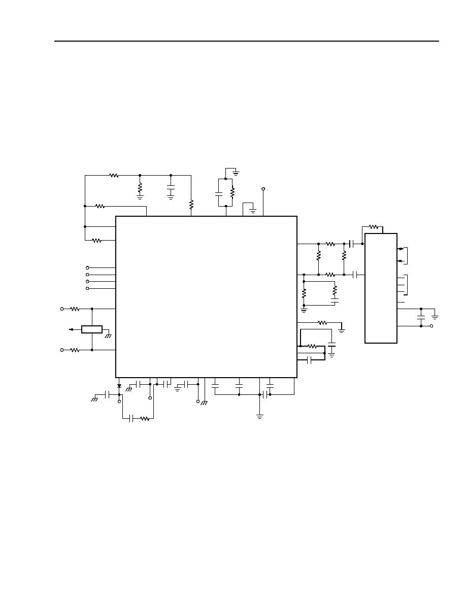
Lucent Technologies Inc.
31
Data Sheet
April 2000
L8560 Low-Power SLIC with Ringing
Applications
(continued)
Power Ringing
(continued)
Reference Designs for ISDN TA Applications
A POTS circuit for reference design is shown in Figure 33. In Figure 33, the L8560 SLIC and T8503 codec are
used. The ac circuit is designed per Bellcore TA-909 with a 600
resistive termination and hybrid circuit, with
the transmit gain set for ≠2 dB and the receive gain set for ≠4 dB. The T8503 codec is compatible with the T7237
U-interface transceiver and the T7256 SCNT1 interface.
12-3345.R (F)
* R
1
= 133 k
for L8560C.
Required only for L8560A/C versions.
Notes:
T
X
= ≠2 dB.
R
X
= ≠4 dB.
Termination = 600
.
Hybrid balance = 600
.
Figure 33. POTS Interface with Balanced Ringing Using L8560 SLIC and T8503 Codec
GSX
VFROP
DX
DR
FSX
MCLK
SYNC
TIP
R
PT
RING
PT
BS1
BS2
BG
ND
AG
ND
VITR
RCVP
TG
VTX
TX1
C
B2
VFXIN
C
F1
CF
1
CF
2
PR
B0
B1
B2
FGND
V
BAT
CONTROL
R
1
(RTS2)*
R
LCTH
C
2
DGND
AGND
V
DD
1
2
4
6, 7
16
PCM
R
2
R
4
C
FB1
C
BS
C
BAT2
C
BAT1
FB1
V
CC
V
BA
T
1
V
BA
T
2
BR
R
PR
R
3
R
TG
DGND
CV
DD
RCVN
C
ST
FSR
C
TG
R
ST
210 k
8.25 k
(RTS3)
562 k
(RTSN)
0.1
µ
F
(RTSN)
124 k
C
4
(CRTSP)
0.1
µ
F
SUPERVISION
OUTPUT
RGDET
NTST
AT
ICM
RT
SP
RT
SN
LC
T
H
DCOUT
I
PROG
R
PROG
14 k
INPUTS
30
L7591
30
0.1
µ
F
0.1
µ
F
0.1
µ
F
100
0.22
µ
F
4.7 nF
C
FB2
4.7 nF
C
F2
0.1
µ
F
FB2
0.47
µ
F
0.1
µ
F
27 pF
4.32 k
R
GN
30.1 k
R
GP
41.2 k
R
GP2
1.21 k
R
RCV
178 k
C
C2
0.1
µ
F
C
C1
0.1
µ
F
R
T6
60.4 k
R
HB1
143 k
HIGHWAY
AND
CLOCK
0.1
µ
F
1/2 T8503
CODEC
(RTSP)
351 k
C
CC
0.1
µ
F
C
GP
220 pF
R
X
71.5 k
R
T3
165 k
L8560A, D, E, F, G

Data Sheet
April 2000
L8560 Low-Power SLIC with Ringing
32
Lucent Technologies Inc.
Applications
(continued)
Power Ringing
(continued)
Table 11. Parts List for Balanced Ringing Using T8503 Codec
* Required for L8560A/L8560C version only.
Use 133 k
for L8560C.
Name
Value
Function
Integrated Circuits
SLIC
L8560
Subscriber line interface circuit (SLIC).
Protector
L7591
Secondary protection.
Codec
T8503
First-generation codec.
Fault Protection
R
PT
30
fusible
Overcurrent protection.
R
PR
30
fusible
Overcurrent protection.
Power Supply
C
BAT1
0.1
µ
F, 20%, 100 V
V
BAT
filter capacitor.
C
BAT2
0.1
µ
F, 20%, 100 V
V
BAT
filter capacitor.
C
CC
0.1
µ
F, 20%, 10 V
V
CC
filter capacitor.
C
F1
0.47
µ
F, 20%, 100 V
With C
F2
, improves idle-channel noise.
C
F2
0.1
µ
F, 20%, 100 V
With C
F1
, improves idle-channel noise.
C
BS
0.22
µ
F, 20%, 100 V
Slows battery switch transition.
C
ST
0.1
µ
F, 20%, 10 V
Loop stability.
R
ST
100
, 1%, 1/8 W
Loop stability.
dc Profile/Ringing
C
FB1
4.7 nF, 20%, 100 V
With C
FB2
, slows rate of forward/reverse battery transition. Sets crest factor of
balanced power ring signal.
C
FB2
4.7 nF, 20%, 100 V
With C
FB1
, slows rate of forward/reverse battery transition. Sets crest factor of
balanced power ring signal.
R
PROG
14 k
, 1%, 1/8 W
Sets dc loop current.
ac Characteristics
R
TG
4.32 k
, 1%, 1/8 W
Sets internal transmit path gain to 19.2.
C
B2
0.1
µ
F, 20%, 10 V
ac/dc separation capacitor.
C
C1
0.1
µ
F, 20%, 10 V
dc blocking capacitor.
C
C2
0.1
µ
F, 20%, 10 V
dc blocking capacitor.
R
T3
165 k
, 1%, 1/8 W
With R
GP
and R
RCV
, sets ac termination impedance.
R
RCV
178 k
, 1%, 1/8 W
With R
GP
and R
T3
, sets receive gain.
R
GP
41.2 k
, 1%, 1/8 W
With R
T3
and R
RCV
, sets ac termination impedance and receive gain.
C
GP
220 pF, 20%, 10 V
Loop stability.
C
TG
*
27 pF, 20%, 10 V
Loop stability.
R
GP2
1.21 k
, 1%, 1/8 W
Loop stability.
R
GN
30.1 k
, 1%, 1/8 W
Compensates for input bias offset at RCVN/RCVP.
R
T6
60.4 k
, 1%, 1/8 W
With R
X
, sets transmit gain in codec.
R
X
71.5 k
, 1%, 1/8 W
With R
T6
, sets transmit gain in codec.
R
HB1
143 k
, 1%, 1/8 W
Sets hybrid balance.
Supervision
R
LCTH
8.25 k
, 1%, 1/8 W
Sets loop closure (off-hook) threshold.
R
1
(RTS2)
210 k
, 1%, 1/8 W
With R
2
, R
3
, and R
4
, sets ring trip threshold.
R
2
(RTSN)
124 k
, 1%, 1/8 W
With R
1
, R
3
, and R
4
, sets ring trip threshold.
C
2
(CRTSN)
0.1
µ
F, 20%, 50 V
With R
2
, sets pole of low-pass ring trip sense filter.
R
3
(RTS3)
562 k
, 1%, 1/8 W
With R
1
, R
2
, and R
4
, sets ring trip threshold.
R
4
(RTSP)
351 k
, 1%, 1/8 W
With R
1
, R
2
, and R
3
, sets ring trip threshold.
C
4
(CRTSP)
0.1
µ
F, 20%, 10 V
With R
4
, sets pole of low-pass ring trip sense filter.
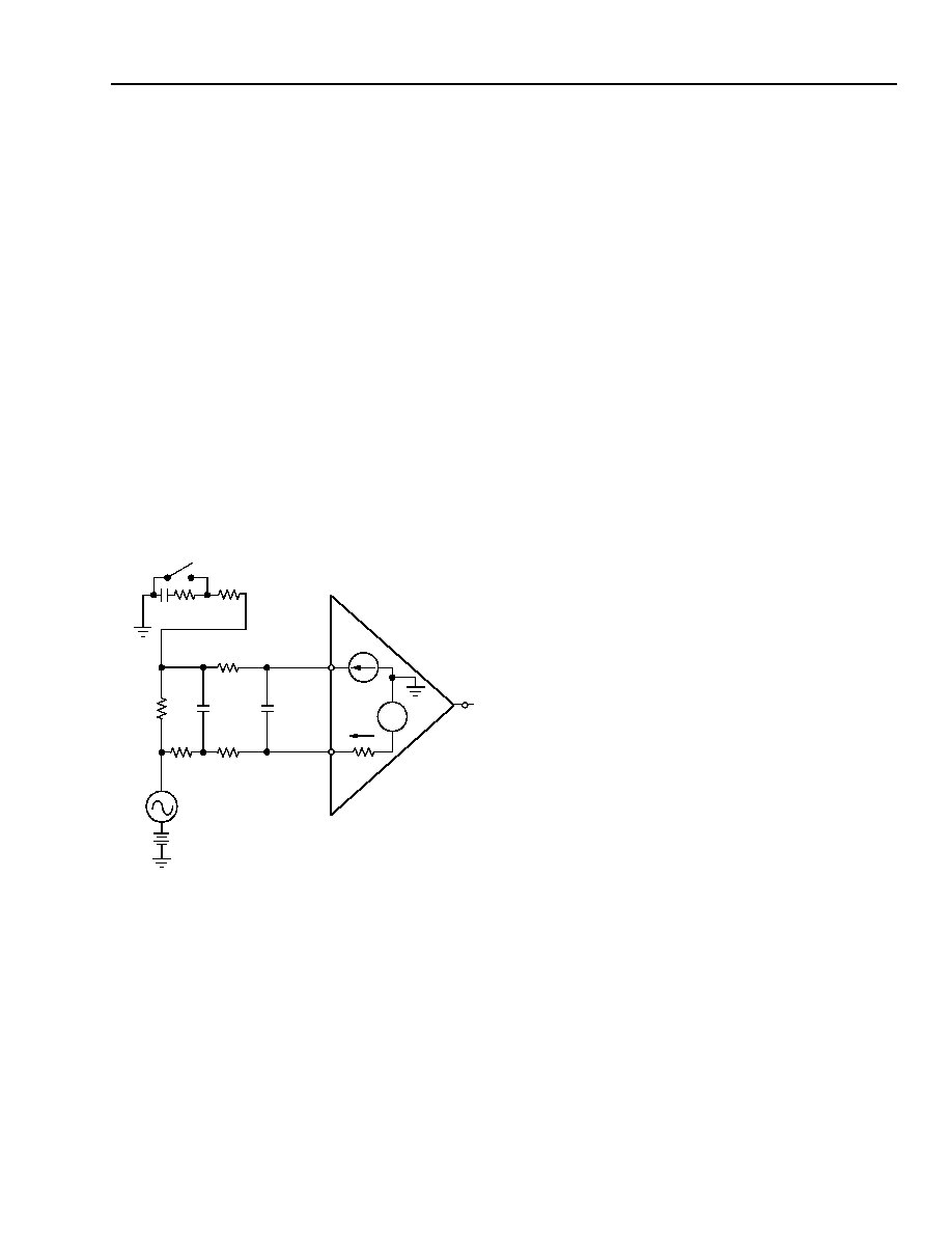
Lucent Technologies Inc.
33
Data Sheet
April 2000
L8560 Low-Power SLIC with Ringing
Applications
(continued)
Design Considerations
Unbalanced Bused Ring Signal Application
The L8560 SLIC can also be used in the standard bat-
tery-backed, unbalanced ringing application. In this
case, the ring signal is generated by a central ring gen-
erator and is bused to individual tip/ring pairs. A ringing
relay is used during ringing to disconnect the SLIC
from, and apply the ring generator to, the tip and ring
pair.
Ring Trip Detection
The ring trip circuit is a comparator that has a special
input section optimized for this application. The equiva-
lent circuit is shown in Figure 34, along with its use
in an application using unbalanced, battery-backed
ringing.
12-3014.c (F)
Figure 34. Ring Trip Equivalent Circuit and
Equivalent Application
The comparator input voltage compliance is V
CC
to
V
BAT
, and the maximum current is 240
µ
A in either
direction. Its application is straightforward. A resistance
(R
TSN
+ R
TS2
) in series with the R
TSN
input establishes a
current that is repeated in the R
TSP
input. A slightly
lower resistance (R
TSP
) is placed in series with the R
TSP
input. When ringing is being injected, no dc current
flows through R
TS1
, so the R
TSP
input is at a lower
potential than R
TSN
. When enough dc loop current
flows, the R
TSP
input voltage increases to trip the com-
parator. In Figure 34, a low-pass filter with a double
pole at 2 Hz was implemented to prevent false ring trip.
The following example illustrates how the detection cir-
cuit in Figure 34 will trip at a 12.5 mA dc loop current
using a ≠48 V battery.
The current I
N
is repeated as I
P
in the positive compar-
ator input. The voltage at comparator input R
TSP
is:
V
RTSP
= V
BAT
+ I
LOOP(dc)
x R
TS1
+ I
P
x R
TSP
Using this equation and the values in the example, the
voltage at input R
TSP
is ≠13.2 V during ringing injection
(I
LOOP(dc)
= 0). Input R
TSP
is therefore at a level of 5 V
below R
TSN
. When enough dc loop current flows
through R
TS1
to raise its dc drop to 5 V, the comparator
will trip.
In this example:
I
LOOP(dc)
=
= 12.5 mA
Except for L8560CAU, the internal voltage for
L8560CAU is ≠5.7 V.
Note that during ringing in this mode of operation, both
the NLC and NRDET circuits are active. During the
actual ringing, NRDET is connected and NLC is iso-
lated from tip and ring by the ring relay; thus, NSTAT
reflects the status at NRDET. During quiet intervals of
ringing, NLC is connected and NRDET is isolated from
tip and ring by the ring relay; thus, NSTAT reflects the
status at NLC. Thus, during ring cadence, the logic
input that drives the ring relay can be used as an indi-
cation as to whether NRDET or NLC appears at output
NSTAT.
A basic loop start reference circuit, using bused
ringing with the L8560 SLIC and T7504 first-generation
codec, is shown in Figure 35. This circuit is designed
for a 600
resistive termination impedance and hybrid
balance. Transmit and receive gains are both set at
0 dB.
+
≠
R
TSP
R
LOOP
15 k
8.2 V
I
P
= I
N
R
TSN
R
TS2
2 M
2 M
C
RTS1
0.022
µ
F
C
RTS2
0.27
µ
F
274 k
PHONE
HOOK SWITCH
RC PHONE
V
RING
V
BAT
NRDET
R
TS1
402
R
TSP
I
N
R
TSN
≠
+
I
N
≠8.2 V ≠ (≠48)
2.289 M
--------------------------------------
=
17.4 µA
=
5 V
402
-----------------
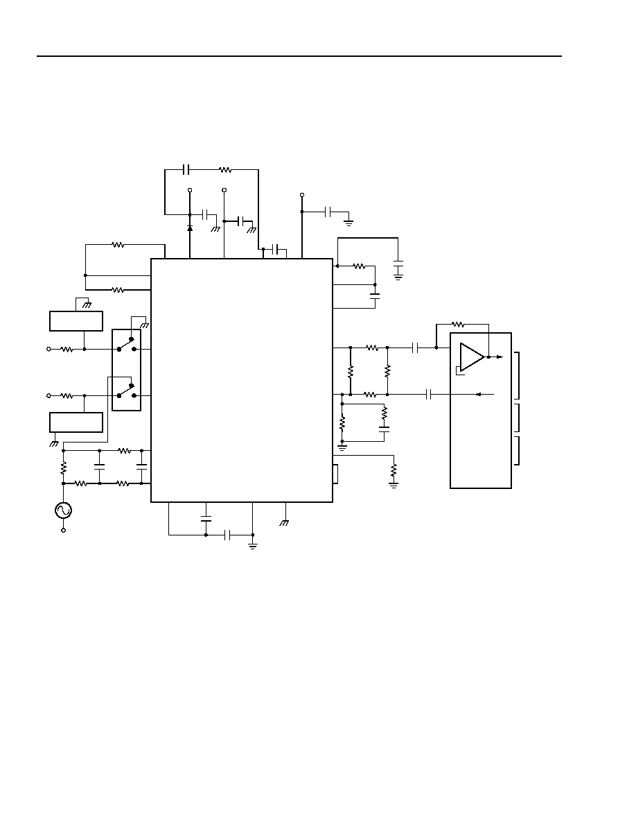
Data Sheet
April 2000
L8560 Low-Power SLIC with Ringing
34
Lucent Technologies Inc.
Applications
(continued)
Design Considerations
(continued)
12-3550 (F)
* Required for L8560A/L8560C version only.
Notes:
T
X
= 0 dB.
R
X
= 0 dB.
Termination = 600
.
Hybrid balance = 600
.
Figure 35. Basic Loop Start Application Circuit Using T7504 Codec and Bused Ringing
R
PROG
14 k
R
LCTH
8.25 k
TIP
R
PT
50
RING R
PR
L7581
RELAY
TIP
V
BAT1
C
BAT1
0.1
µ
F
V
BAT1
V
BAT2
C
BAT2
0.1
µ
F
V
BAT2
C
CC
0.1
µ
F
V
CC
V
CC
RCVN
DCOUT
LCTH
50
RING
RTSP
R
TS1
402
C
RTS2
0.27
µ
F
RTSN
R
TS2
274 k
R
TSN
2.0 M
V
RING
V
BAT
CF2
CF1
C
F1
0.47
µ
F
AGND
BGND
I
PROG
VITR
RCVP
R
T3
174 k
R
T6
49.9 k
R
RCV
100 k
R
HB1
75.0 k
VFXIN
R
X
75.0 k
GSX
V
FRO
DX
DR
FSE
FSEP
MCLK
ASEL
1/4 T7504
CODEC
CONTROL
INPUTS
PCM
HIGHWAY
SYNC
AND
CLOCK
≠
+
L8560
SLIC
B1
B0
CONTROL
INPUTS
NSTAT
SUPERVISION
OUTPUTS
C
RTS1
0.022
µ
F
TXI
V
TX
C
B2
0.1
µ
F
R
TSP
2.0 M
C
F2
0.1
µ
F
R
GX
4.32 k
TG
BS1
BS2
C
BS
0.22
µ
F
+2.4 V
C
C1
0.1
µ
F
C
C2
0.1
µ
F
R
GN
29.4 k
R
GP
41.2 k
100
C
ST
0.1
µ
F
C
GP
220 pF
R
GP2
1.21 k
C
TG
27 pF*
R
ST
CROWBAR
PROTECTOR
CROWBAR
PROTECTOR
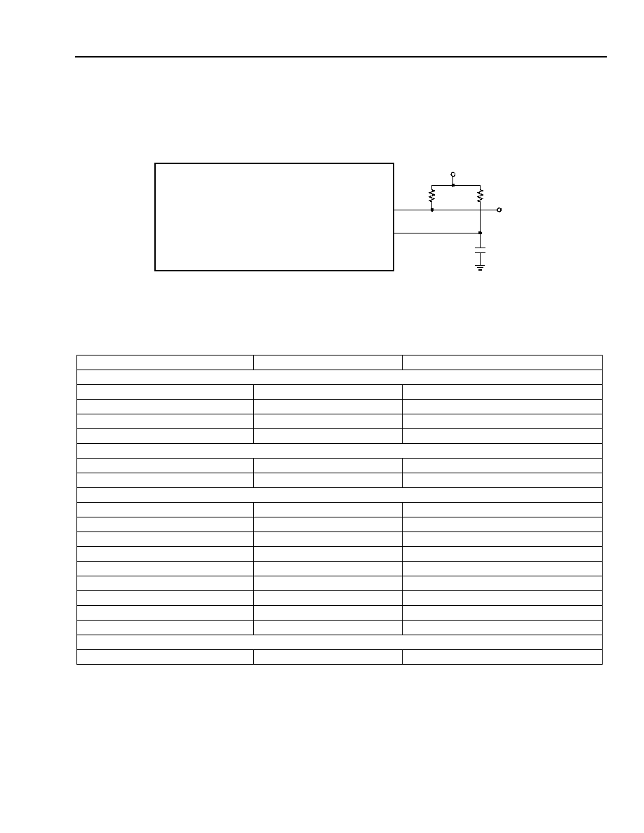
Lucent Technologies Inc.
35
Data Sheet
April 2000
L8560 Low-Power SLIC with Ringing
Applications
(continued)
Design Considerations
(continued)
Figure 36 shows the ground start application.
12-3547.a.c (F)
Figure 36. Ground Start Application Circuit
Table 12. Parts List for Loop Start with Bused Ringing and Ground Start Applications
* Contact your Lucent Technologies account representative for protector recommendations. Choice of this (and all) component(s) should be
evaluated and confirmed by the customer prior to use in any field or laboratory system. Lucent does not recommend use of this part in the
field without performance verification by the customer. This device is suggested by Lucent for customer evaluation. The decision to use a
component should be based solely on customer evaluation.
Required for L8560A/L8560C version only.
Name
Value
Function
Integrated Circuits
SLIC
--
Subscriber line interface circuit (SLIC).
Protector
Crowbar protector*
Secondary protection.
Ringing Relay
L7581
Switches ringing signals.
Codec
T7504
First-generation codec.
Fault Protection
R
PT
50
PTC or fusible
Protection resistor.
R
PR
50
PTC or fusible
Protection resistor.
Power Supply
C
BAT1
0.1
µ
F, 20%, 100 V
V
BAT
filter capacitor.
C
BAT2
0.1
µ
F, 20%, 100 V
V
BAT
filter capacitor.
C
CC
0.1
µ
F, 20%, 10 V
V
CC
filter.
C
F1
0.47
µ
F, 20%, 100 V
With C
F2
, improves idle-channel noise.
C
F2
0.1
µ
F, 20%, 100 V
With C
F1
, improves idle-channel noise.
C
BS
0.22
µ
F, 20%, 100 V
Slows battery switch transition.
C
ST
0.1
µ
F, 20%, 10 V
Loop stability.
R
ST
100
, 1%, 1/8 W
Loop stability.
C
TG
27 pF, 20%, 10 V
Loop stability.
dc Profile
R
PROG
14 k
, 1%, 1/8 W
Sets dc loop current.
V
CC
0.47
µ
F
C
ICM
GROUND START
APPLICATION CIRCUIT
R
GDET
ICM
R
GDET
R
ICM2
71.5 k
100 k
R
GDET

Data Sheet
April 2000
L8560 Low-Power SLIC with Ringing
36
Lucent Technologies Inc.
Applications
(continued)
Design Considerations
(continued)
Table 12. Parts List for Loop Start with Bused Ringing and Ground Start Applications (continued)
Name
Value
Function
ac Characteristics
R
GX
4.32 k
, 1%, 1/8 W
Sets internal transmit path gain of 9.6.
C
B2
0.1
µ
F, 20%, 10 V
ac/dc separation capacitor.
R
T3
174 k
, 1%, 1/8 W
With R
GP
and R
RCV
, sets ac termination impedance.
R
RCV
100 k
, 1%, 1/8 W
With R
GP
and R
T3
, sets receive gain.
R
GP
41.2 k
, 1%, 1/8 W
With R
T3
and R
RCV
, sets ac termination impedance and receive gain.
C
GP
220 pF, 20%, 10 V
Loop stability.
R
GP2
1.21 k
, 1%, 1/8 W
Loop stability.
R
GN
29.4 k
, 1%, 1/8 W
Compensates for input bias offset at RCVN/RCVP.
C
C1
0.1
µ
F, 20%, 10 V
dc blocking capacitor.
C
C2
0.1
µ
F, 20%, 10 V
dc blocking capacitor.
R
T6
49.9 k
, 1%, 1/8 W
With R
X
, sets transmit gain in codec.
R
X
75.0 k
, 1%, 1/8 W
With R
T6
, sets transmit gain in codec.
R
HB1
75.0 k
, 1%, 1/8 W
Sets hybrid balance.
Supervision
R
LCTH
8.25 k
, 1%, 1/8 W
Sets loop closure (off-hook) threshold.
R
TS1
402
, 5%, 2 W
Ringing source series resistor.
R
TS2
274 k
, 1%, 1/8 W
With C
RTS2
, forms first pole of a double pole, 2 Hz ring trip sense filter.
C
RTS1
0.022
µ
F, 20%, 5 V
With R
TSN
and R
TSP
, forms second 2 Hz filter pole.
C
RTS2
0.27
µ
F, 20%, 100 V
With R
TS2
, forms first 2 Hz filter pole.
R
TSN
2 M
, 1%, 1/8 W
With C
RTS1
and R
TSP
, forms second 2 Hz filter pole.
R
TSP
2 M
, 1%, 1/8 W
With C
RTS1
and R
TSN
,
forms second 2 Hz filter pole.
Ground Start
C
ICM
0.47
µ
F, 20%, 10 V
Provides 60 Hz filtering for ring ground detection.
R
GDET
100 k
, 20%, 1/8 W
Digital output pull-up resistor.
R
ICM2
71.5 k
, 1%, 1/8 W
Sets ring ground detection threshold.

Data Sheet
April 2000
Lucent Technologies Inc.
37
L8560 Low-Power SLIC with Ringing
Applications
(continued)
Design Considerations
(continued)
Table 13 shows the design parameters of the application circuit shown in Figure 35. Components that are adjusted
to program these values are also shown.
Table 13. 600
Design Parameters
Design Parameter
Parameter Value
Components Adjusted
Loop Closure Threshold
10 mA
R
LCTH
dc Loop Current Limit
25 mA
R
PROG
dc Feed Resistance
55
--
2-wire Signal Overload Level
3.14 dBm
--
ac Termination Impedance
600
R
T3
, R
GP
, R
RCV
Hybrid Balance Line Impedance
600
R
HB1
Transmit Gain
0 dB
R
T6
, R
X
Receive Gain
0 dB
R
RCV
, R
GP
, R
T3
ac Design
There are four key ac design parameters. Termination
impedance is the impedance looking into the 2-wire
port of the line card. It is set to match the impedance of
the telephone loop in order to minimize echo return to
the telephone set. Transmit gain is measured from the
2-wire port to the PCM highway, while receive gain is
done from the PCM highway to the transmit port.
Finally, the hybrid balance network cancels the
unwanted amount of the receive signal that appears at
the transmit port.
At this point in the design, the codec needs to be
selected. The discrete network between the SLIC and
the codec can then be designed. Below is a brief codec
feature and selection summary.
First-Generation Codecs
These perform the basic filtering, A/D (transmit), D/A
(receive), and
µ
-law/A-law companding. They all have
an op amp in front of the A/D converter for transmit gain
setting and hybrid balance (cancellation at the summing
node). Depending on the type, some have differential
analog input stages, differential analog output stages,
and
µ
-law/A-law selectability. This generation of codec
has the lowest cost. It is most suitable for applications
with fixed gains, termination impedance, and hybrid bal-
ance.
Second-Generation Codecs
This class of devices includes a microprocessor inter-
face for software control of the gains and hybrid bal-
ance. The hybrid balance is included in the device. ac
programmability adds application flexibility and saves
several passive components. It also adds several I/O
latches that are needed in the application. It does not
have the transmit op amp, since the transmit gain and
hybrid balance are set internally.
Third-Generation Codecs
This class of devices includes the gains, termination im-
pedance, and hybrid balance--all under microproces-
sor control. Depending on the device, it may or may not
include latches.
In the codec selection, increasing software control and
flexibility are traded for device cost. To help decide, it
may be useful to consider the following: Will the appli-
cation require only one value for each gain and imped-
ance? Will the board be used in different countries with
different requirements? Will several versions of the
board be built? If so, will one version of the board be
most of the production volume? Does the application
need only real termination impedance? Does the hybrid
balance need to be adjusted in the field?
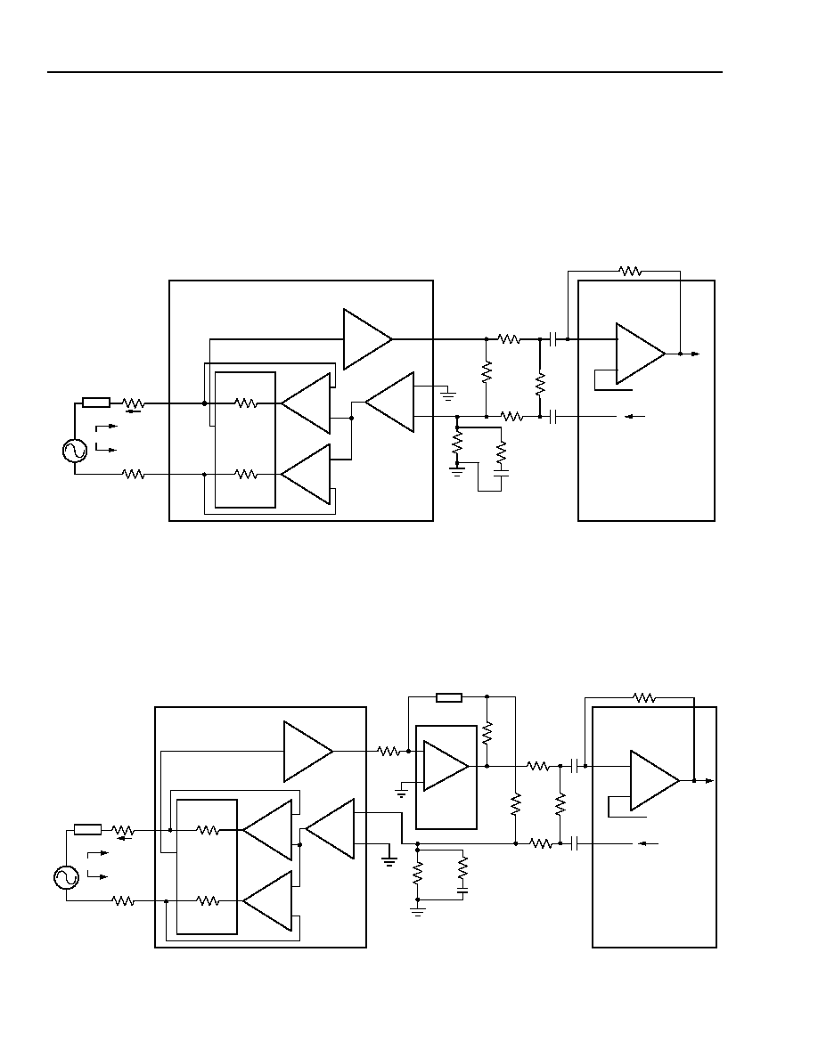
Data Sheet
April 2000
L8560 Low-Power SLIC with Ringing
38
Lucent Technologies Inc.
Applications
(continued)
ac Design
(continued)
ac equivalent circuits using a T7504 codec (V
CC
only) are shown in Figures 37 and 38. Use the following two equa-
tions for Figure 37 below:
R
STP
= 1 k
x {[R
GP
(k
) || R
RCV
(k
)]/24 (k
)}
C
STP
= 270 pF/{[R
GP
(k
) || R
RCV
(k
)]/24 (k
)}
12-2554.p (F)
Figure 37. ac Equivalent Circuit Not Including Spare Op Amp
Use the following two equations for Figure 38 below:
R
STN
= 1 k
x {[R
GN
(k
) || R
RCV
(k
)]/24 (k
)}
C
STN
= 270 pF/{[R
GN
(k
) || R
RCV
(k
)]/24 (k
)}
12-3013.j (F)
Figure 38. ac Equivalent Circuit Including Spare Op Amp
R
P
Z
T
+
≠
R
P
V
T/R
I
T/R
V
S
Z
T/R
+
≠
RING
A
V
= ≠1
A
V
= 1
VITR
≠
+
+
≠
CURRENT
SENSE
TIP
+
≠
R
T3
R
RCV
R
HB1
R
T6
RCVN
RCVP
R
X
VGSX
VFXIN
VFR
1/2 T7504 CODEC
R
GP
+2.4 V
≠0.400 V/mA
A
V
= 4
L8560 SLIC
VFXIP
R
STP
C
STP
+
≠
Z
T5
SN
AGND
R
T5X
C
STN
R
P
Z
T
+
≠
R
P
V
T/R
I
T/R
V
S
Z
T/R
+
≠
RING
A
V
= ≠1
A
V
= 1
VITR
≠
+
+
≠
CURRENT
SENSE
TIP
R
T4
+
≠
R
T3
R
RCV
R
HB1
R
T6
RCVN
RCVP
R
X
VGSX
VFXIN
VFRO
1/4 T7504 CODEC
R
GN
+2.4 V
L8560 SLIC
A
V
= 4
R
STN
XMT
VFXIP

Lucent Technologies Inc.
39
Data Sheet
April 2000
L8560 Low-Power SLIC with Ringing
Applications
(continued)
Design Examples
In the preceding examples, use of a first-generation
codec is shown. The equations for second- and third-
generation codecs are simply subsets of these. There
are two examples below. The first shows the simplest
circuit, which uses a minimum number of discrete com-
ponents to synthesize a real termination impedance.
The second example shows the use of the uncommit-
ted op amp to synthesize a complex termination. The
design has been automated in a DOS-based program,
available on request.
Example 1, Real Termination
The following design equations refer to the circuit in
Figure 37. Use these to synthesize real termination
impedance.
Termination impedance:
z
T
=
Receive gain:
Transmit gain:
Hybrid balance:
h
bal
= 20log
h
bal
= 20log
To optimize the hybrid balance, the sum of the currents
at the VFX input of the codec op amp should be set to
0. The expression for ZHB becomes:
Example 2, Complex Termination
For complex termination, the spare op amp may be
used (see Figure 38).
= 2R
P
+ k(Z
T5
)
g
tx
=
The hybrid balance equation is the same as in Exam-
ple 1.
Example 3, Complex Termination Without Spare Op
Amp
The gain shaping necessary for a complex termination
impedance may be done without using the spare op
amp by shaping across the Ax amplifier at nodes TG
and VTX. This is a recommended approach.
V
T/R
I
T/R
≠
------------
z
T
2R
P
3200
1
R
T 3
R
G P
---------
R
T 3
R
R C V
------------
+
+
-----------------------------------
+
=
g
rcv
V
T/R
V
FR
------------
=
g
rcv
8
1
R
R CV
R
T 3
-----------
R
R C V
R
G P
------------
+
+
1
z
T
Z
T/R
---------
+
------------------------------------------------------------------
=
g
tx
V
GSX
V
T/R
-----------
=
g
t x
R
X
≠
R
T 6
---------
400
Z
T/R
---------
◊
=
R
X
R
HB1
---------------
g
tx
≠
g
rcv
◊
V
GSX
V
F R
---------------
R
H B 1
k
( )
R
X
g
tx
g
rcv
◊
-------------------
=
z
T
2R
P
3200
1
R
T 3
R
G N
---------
R
T 3
R
R C V
------------
+
+
-----------------------------------
Z
T 5
R
T4
---------
(
)
+
=
g
rcv
8
1
R
RCV
R
T3
--------------
R
RCV
R
G N
--------------
+
+
1
z
T
Z
T/R
----------
+
-----------------------------------------------------------------------------
=
R
X
R
T6
---------
400
Z
T/R
----------
◊
Z
T 5
R
T4
---------
◊
1
R
T5X
Z
T5
--------------
R
T5X
R
T3
R
G
N
||
R
RCV
+
----------------------------------------------------
+
+
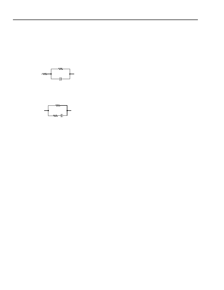
40
40
Lucent Technologies Inc.
Data Sheet
April 2000
L8560 Low-Power SLIC with Ringing
Applications
(continued)
Design Examples
(continued)
Complex Termination Impedance Design Example
Using L8560 Without Spare Op Amp
Complex termination is specified in the form:
5-6396(F)
To work with this application, convert termination to the
form:
5-6398(F)
where:
R
1
¥ = R
1
+ R
2
R
2
¥ =
(R
1
+ R
2
)
C¥ =
C
ac Interface Using First-Generation Codec
R
TGP
/R
TGS
/C
GS
(Z
TG
): These components give gain
shaping to get good gain flatness. These components
are a scaled version of the specified complex termina-
tion impedance.
Note for pure (600
) resistive terminations, compo-
nents R
TGS
and C
GS
are not used. Resistor R
TGP
is
used and is still 4.32 k
.
R
X
/R
T6
: With other components set, the transmit gain
(for complex and resistive terminations) R
X
and R
T6
are
varied to give specified transmit gain.
R
T3
/R
RCV
/R
GP
: For both complex and resistive termina-
tions, the ratio of these resistors set the receive gain.
For resistive terminations, the ratio of these resistors
set the return loss characteristic. For complex termina-
tions, the ratio of these resistors set the low-frequency
return loss characteristic.
C
N
/R
N1
/R
N2
: For complex terminations, these compo-
nents provide high-frequency compensation to the
return loss characteristic.
For resistive terminations, these components are not
used and R
CVN
is connected to ground via a resistor.
R
HB
: Sets hybrid balance for all terminations.
Set Z
TG
--gain shaping:
Z
TG
= R
TGP
|| R
TGS
+ C
GS
which is a scaled version of
Z
T/R
(the specified termination resistance) in the
R
1
¥ || R
2
¥ + C¥ form.
R
TGP
must be 4.32 k
to set SLIC transconductance to
400 V/A
R
TGP
= 4.32 k
At dc, C
TGS
and C¥ are open.
R
TGP
= M x R1¥
where M is the scale factor.
M =
It can be shown:
R
TGS
= M x R2¥
and
C
TGS
=
R
2
C
R
1
R
1
¥
C¥
R
2
¥
R
1
R
2
-------
R
2
R
1
R
2
+
---------------------
2
4320
R
1
--------------
C
M
------
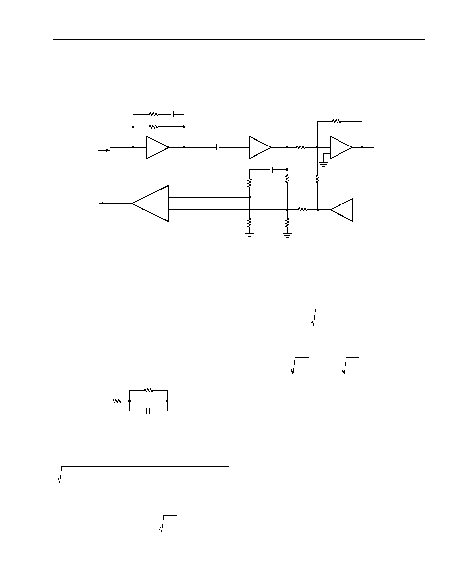
Data Sheet
April 2000
Lucent Technologies Inc.
41
L8560 Low-Power SLIC with Ringing
Applications
(continued)
Design Examples
(continued)
5-6400.b (F)
Figure 39. Interface Circuit Using First-Generation Codec (Blocking Capacitors Not Shown)
0.1
µ
F
R
TGS
V
TX
R
TGP
= 4.32 k
T
XI
V
ITR
R
T6
R
x
R
T3
R
HB
CODEC
OUTPUT
DRIVE
AMP
CODEC
OP AMP
≠
+
19.2
C
N
R
N1
R
N2
R
GP
R
RCV
RCVN
RCVP
≠I
T/R
207.36
C
G
Transmit Gain
Transmit gain will be specified as a gain from T/R to
PCM, T
X
(dB). Since PCM is referenced to 600
and
assumed to be 0 dB, and in the case of T/R being refer-
enced to some complex impedance other than 600
resistive, the effects of the impedance transformation
must be taken into account.
Again, specified complex termination impedance at T/R
is of the form:
5-6396(F)
First, calculate the equivalent resistance of this net-
work at the midband frequency of 1000 Hz.
R
EQ
=
Using R
EQ
, calculate the desired transmit gain, taking
into account the impedance transformation:
T
X
(dB) = T
X (specified[dB])
+ 20 log
T
X (specified[dB])
is the specified transmit gain. 600
is the
impedance at the PCM and R
EQ
is the impedance at
Tip and ring. 20 log
represents the power
loss/gain due to the impedance transformation.
Note in the case of a 600
pure resistive termination
at T/R 20 log
= 20 log
= 0.
Thus, there is no power loss/gain due to impedance
transformation and T
X
(dB) = T
X (specified[dB])
.
Finally, convert T
X
(dB) to a ratio, g
TX
:
T
X
(dB) = 20 log g
TX
The ratio of R
X
/R
T6
is used to set the transmit gain:
= g
TX
∑
∑
with a quad Lucent codec such as T7504:
R
X
< 200 k
R
2
C
R
1
2
f
(
)
2
C
12
R
1
R
22
R
1
R
2
+
+
1
2
f
(
)
2
R
22
C
12
+
-----------------------------------------------------------------------------
2
2
f
R
22
C
1
1
2
f
(
)
2
R
22
C
12
+
---------------------------------------------------
2
+
600
R
EQ
-----------
600
R
EQ
-----------
600
R
EQ
-----------
600
600
----------
R
X
R
T6
----------
207.36
19.2
------------------
1
M
-----

42
42
Lucent Technologies Inc.
Data Sheet
April 2000
L8560 Low-Power SLIC with Ringing
Applications
(continued)
Design Examples
(continued)
Receive Gain
Ratios of R
RCV
, R
T3
, R
GP
will set both the low-frequency
termination and receive gain for the complex case. In
the complex case, additional high-frequency compen-
sation, via C
N
, R
N1
, and R
N2
, is needed for the return
loss characteristic. For resistive termination, C
N
, R
N1
,
and R
N2
are not used and R
CVN
is tied to ground via a
resistor.
Determine the receive gain, g
RCV
, taking into account
the impedance transformation in a manner similar to
transmit gain.
R
X
(dB) = R
X (specified[dB])
+ 20 log
R
X
(dB) = 20 log g
RCV
Then:
g
RCV
=
and low-frequency termination
Z
TER(low)
=
+ 2R
P
Z
TER(low)
is the specified termination impedance assum-
ing low frequency (C or C¥ is open).
R
P
is the series protection resistor.
These two equations are best solved using a computer
spreadsheet.
Next, solve for the high-frequency return loss compen-
sation circuit, C
N
, R
N1
, and R
N2
:
C
N
R
N2
=
C
G
R
TGP
R
N1
= R
N2
There is an input offset voltage associated with nodes
R
CVN
and R
CVP
. To minimize the effect of mismatch of
this voltage at T/R, the equivalent resistance to ac
ground at R
CVN
should be approximately equal to that
at R
CVP
. Refer to Figure 40 on page 43 (with dc block-
ing capacitors). To meet this requirement, R
N2
= R
GP
||
R
T3
.
Hybrid Balance
Set the hybrid cancellation via R
HB
.
R
HB
=
R
EQ
600
-----------
4
1
R
RCV
R
T3
---------------
R
RCV
R
GP
---------------
+
+
------------------------------------------------
3200
1
R
T3
R
GP
------------
R
T3
R
RCV
---------------
+
+
--------------------------------------------
2R
P
3200
-------------
3200
2R
P
-------------
R
T GS
R
T GP
--------------
1
≠
R
X
g
RCV
g
TX
◊
-------------------------------
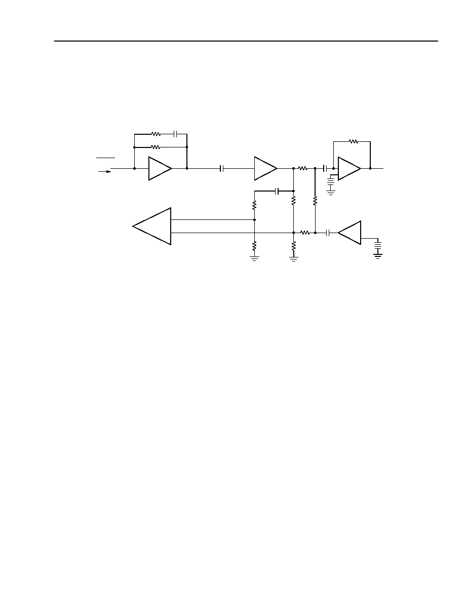
Lucent Technologies Inc.
43
Data Sheet
April 2000
L8560 Low-Power SLIC with Ringing
Applications
(continued)
Design Examples
(continued)
Blocking Capacitors
5-6401b(F)
Figure 40. ac Interface Using First-Generation Codec (Including Blocking Capacitors) for Complex
Termination Impedance
If a 5 V only codec such as the Lucent T7504 is used, dc blocking capacitors must be added as shown in Figure
40. This is because the codec is referenced to 2.5 V and the SLIC to ground--with the ac coupling, a dc bias at
T/R is eliminated and power associated with this bias is not consumed.
Typically, values of 0.1 µF to 0.47 µF capacitors are used for dc blocking. The addition of blocking capacitors will
cause a shift in the return loss and hybrid balance frequency response toward higher frequencies, degrading the
lower-frequency response. The lower the value of the blocking capacitor, the more pronounced the effect is, but
the cost of the capacitor is lower. It may be necessary to scale resistor values higher to compensate for the
low-frequency response. This effect is best evaluated via simulation. A
PSPICE
* model for the L8560 is available.
Design equation calculations seldom yield standard component values. Conversion from the calculated value to
standard value may have an effect on the ac parameters. This effect should be evaluated and optimized via simu-
lation.
*
PSPICE
is a registered trademark of MicroSim Corporation.
0.1
µ
F
R
TGS
V
TX
R
TGP
= 4.32 k
T
XI
V
ITR
R
T6
R
x
R
T3
R
HB
CODEC
OUTPUT
DRIVE
AMP
CODEC
OP AMP
≠
+
19.2
C
N
R
N1
R
N2
R
GP
R
RCV
RCVN
RCVP
≠I
T/R
207.36
C
GS
C
B1
2.5 V
C
B2
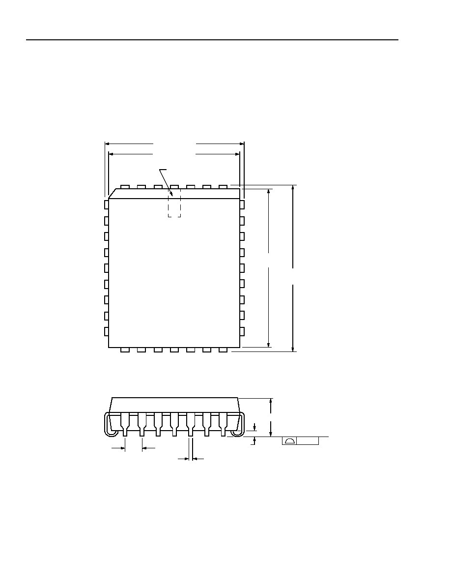
Data Sheet
April 2000
L8560 Low-Power SLIC with Ringing
44
Lucent Technologies Inc.
Outline Diagrams
32-Pin PLCC
Dimensions are in millimeters.
Note: The dimensions in this outline diagram are intended for informational purposes only. For detailed schemat-
ics to assist your design efforts, please contact your Lucent Technologies Sales Representative.
5-3813r2 (F)
0.10
SEATING PLANE
0.38 MIN
TYP
1.27 TYP
0.330/0.533
1
4
30
5
13
21
29
14
20
12.446
±
0.127
11.430
±
0.076
PIN #1 IDENTIFIER
ZONE
14.986
±
0.127
13.970
±
0.076
3.175/3.556
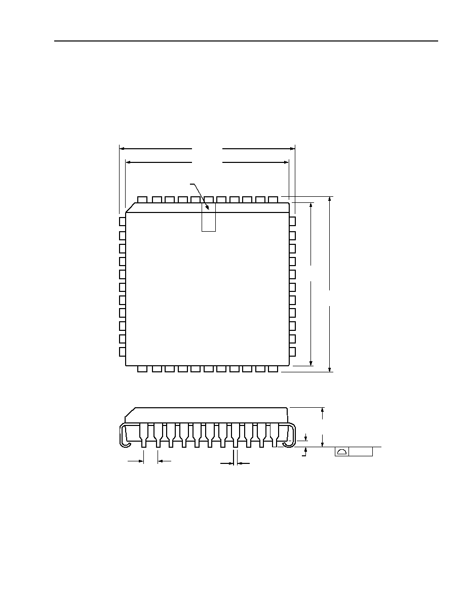
Lucent Technologies Inc.
45
Data Sheet
April 2000
L8560 Low-Power SLIC with Ringing
Outline Diagrams
(continued)
44-Pin PLCC
Dimensions are in millimeters.
Note: The dimensions in this outline diagram are intended for informational purposes only. For detailed schemat-
ics to assist your design efforts, please contact your Lucent Technologies Sales Representative.
5-2506r.8(F)
4.57
MAX
1.27 TYP
0.53
MAX
0.10
SEATING PLANE
0.51 MIN
TYP
1
6
40
7
17
29
39
18
28
PIN #1 IDENTIFIER
ZONE
16.66 MAX
17.65 MAX
16.66
MAX
17.65
MAX

Data Sheet
April 2000
L8560 Low-Power SLIC with Ringing
Lucent Technologies Inc. reserves the right to make changes to the product(s) or information contained herein without notice. N o liability is assumed as a result of their use or application. No
rights under any patent accompany the sale of any such product(s) or information.
Copyright © 2000 Lucent Technologies Inc.
All Rights Reserved
April 2000
DS00-172ALC (Replaces DS99-124ALC)
For additional information, contact your Microelectronics Group Account Manager or the following:
INTERNET: http://www.lucent.com/micro
E-MAIL: docmaster@micro.lucent.com
N. AMERICA:
Microelectronics Group, Lucent Technologies Inc., 555 Union Boulevard, Room 30L-15P-BA, Allentown, PA 18103
1-800-372-2447, FAX 610-712-4106 (In CANADA: 1-800-553-2448, FAX 610-712-4106)
ASIA PACIFIC: Microelectronics Group, Lucent Technologies Singapore Pte. Ltd., 77 Science Park Drive, #03-18 Cintech III, Singapore 118256
Tel. (65) 778 8833, FAX (65) 777 7495
CHINA: Microelectronics Group, Lucent Technologies (China) Co., Ltd., A-F2, 23/F, Zao Fong Universe Building, 1800 Zhong Shan Xi Road, Shanghai
200233 P. R. China Tel. (86) 21 6440 0468, ext. 316, FAX (86) 21 6440 0652
JAPAN: Microelectronics Group, Lucent Technologies Japan Ltd., 7-18, Higashi-Gotanda 2-chome, Shinagawa-ku, Tokyo 141, Japan
Tel. (81) 3 5421 1600, FAX (81) 3 5421 1700
EUROPE: Data Requests: MICROELECTRONICS GROUP DATALINE: Tel. (44) 7000 582 368, FAX (44) 1189 328 148
Technical Inquiries: GERMANY: (49) 89 95086 0 (Munich), UNITED KINGDOM: (44) 1344 865 900 (Ascot),
FRANCE: (33) 1 40 83 68 00 (Paris), SWEDEN: (46) 8 594 607 00 (Stockholm), FINLAND: (358) 9 4354 2800 (Helsinki),
ITALY: (39) 02 6608131 (Milan), SPAIN: (34) 1 807 1441 (Madrid)
Ordering Information
Device Code Description Package Comcode
LUCL8560AAU-D Low-power SLIC (Dry-bagged) 32-Pin PLCC 107957375
LUCL8560AAU-DT Low-power SLIC (Tape and Reel, Dry-bagged) 32-Pin PLCC 107957383
LUCL8560AP-D Low-power SLIC (Dry-bagged) 44-Pin PLCC 107891111
LUCL8560AP-DT Low-power SLIC (Tape and Reel, Dry-bagged) 44-Pin PLCC 107891129
LUCL8560CAU-D Low-power SLIC (Dry-bagged) 32-Pin PLCC 107953390
LUCL8560CAU-DT Low-power SLIC (Tape and Reel, Dry-bagged) 32-Pin PLCC 107953408
LUCL8560DAU-D Low-power SLIC (Dry-bagged) 32-Pin PLCC 108130576
LUCL8560DAU-DT Low-power SLIC (Tape and Reel, Dry-bagged) 32-Pin PLCC 108130584
LUCL8560EP-D Low-power SLIC (Dry-bagged) 44-Pin PLCC 108133000
LUCL8560EP-DT Low-power SLIC (Tape and Reel, Dry-bagged) 44-Pin PLCC 108133018
LUCL8560FAU-D Low-power SLIC (Dry-bagged) 32-Pin PLCC 108190885
LUCL8560FAU-DT Low-power SLIC (Tape and Reel, Dry-bagged) 32-Pin PLCC 108190893
LUCL8560GP-D Low-power SLIC (Dry-bagged) 44-Pin PLCC 108190935
LUCL8560GP-DT Low-power SLIC (Tape and Reel, Dry-bagged) 44-Pin PLCC 108190943