Document Outline
- Features
- Description
- Pin Information
- Coding Information
- Absolute Maximum Ratings (TA = 25 ∞C)
- Recommended Operating Conditions
- Electrical Characteristics
- Test Configurations
- Functional Description
- Chip Set Performance Specifications
- Applications
- dc Characteristics
- dc Applications
- Outline Diagrams
- Ordering Information
- List of Figures
- List of Tables
- Table 1. Pin Descriptions
- Table 2. Input State Coding
- Table 3. Supervision Coding
- Table 4. Power Supply
- Table 5. 2-Wire Port
- Table 6. Analog Pin Characteristics
- Table 7. ac Feed Characteristics
- Table 8. Logic Inputs (B0, B1, EN, RD1I, RD2I, and RD3I) and Outputs (NSTAT and NTSD)
- Table 9. Drivers (RD1O, RD2O, and RD3O)
- Table 10. LED Driver (NLED)
- Table 11. Timing Requirements (DI, EN, DO, and RD), CCLK = 2.048 MHz
- Table 12. Gain
- Table 13. Gain FlatnessÑIn Band
- Table 14. Gain FlatnessÑOut of BandÑLow Frequencies
- Table 15. Parts List for Loop Start Application
- Table 16. 200 Ohm + 680 Ohm || 0.1 microfarad Design Parameters
- Table 17. Power Connections
- Table 18. RPWR = 2600 Ohm
- Table 19. RPWR = 2200 Ohm
- Table 20. RPWR = 1800 Ohm
- Table 21. RPWR = 4400 Ohm
- Table 22. RPWR = 2310 Ohm (RPWR = 2200 Ohm + 5%)
- Table 23. RPWR = 2090 Ohm (RPWR = 2200 Ohm Ö 5%)
- Table 24. Valid Data at NSTAT and NTSD
- Contact Us

Data Sheet
August 1999
L8567 SLIC for
People's Republic of China Applications
Features
s
Low active power (typical 149 mW during on-hook
transmission)
s
Sleep state for low idle power (47 mW typical)
s
Quiet tip/ring polarity reversal
s
Distortion-free on-hook transmission
s
≠35 V to ≠65 V battery operation
s
Convenient operating states:
-- Forward active
-- Polarity reversal active
-- Sleep
-- Forward disconnect
s
Supervision functions:
-- Fixed threshold off-hook detector with
longitudinal rejection and hysteresis
-- Ring trip detector
-- Thermal shutdown indication
s
Adjustable loop current limit
s
Three driver outputs for relay driver
s
LED driver output to indicate off-hook
s
Latched parallel data interface
s
Battery and +5 V required:
-- Optional auxiliary lower voltage battery to
reduce short loop power
s
≠40 ∞C to +85 ∞C operational temperature range
s
User-selectable power management techniques
s
Thermal protection
s
32-pin PLCC or 44-pin PLCC packaging
Description
General
This electronic subscriber loop interface circuit
(SLIC) is optimized for low cost and low power con-
sumption while providing a full-feature set.
Included in the feature set is quiet reverse battery.
Quiet polarity reversal is possible because the ac
path is uninterrupted during transmission. The dc
loop current limit is user-adjustable via a single exter-
nal resistor. The maximum battery voltage is speci-
fied as ≠65 V for long loop applications. The L8567
supports on-hook transmission.
The total short loop off-hook power may be reduced
by use of a lower-voltage auxiliary battery supply. If,
when using the 32-pin PLCC, the user does not wish
to supply an auxiliary battery, the component of the
total short loop off-hook power that is dissipated on
the L8567 SLIC is controlled by use of an external
power resistor. With the 44-pin PLCC, a power resis-
tor is not necessary.
Included are both the loop closure and ring trip
supervision functions. The loop closure threshold is
fixed internally, which eliminates the need for an
external precision resistor to set the threshold. To
minimize noise at the supervision output, hysteresis
is included on the loop closure function. The loop clo-
sure and ring trip outputs are multiplexed into a sin-
gle NSTAT output. Also included is a thermal
shutdown mechanism. If device temperature exceeds
165 ∞C, as may be the case under an extended
power cross fault, the SLIC will shut down (i.e., enter
a high-impedance state) to provide protection against
the fault. A logic output will indicate the SLIC is in
thermal shutdown.

2
Lucent Technologies Inc.
Data Sheet
August 1999
People's Republic of China Applications
L8567 SLIC for
Table of Contents
Contents
Page
Features ......................................................................1
Description...................................................................1
General...................................................................1
Application for People's Republic of China ............4
Pin Information ............................................................6
Coding Information ......................................................9
Absolute Maximum Ratings.......................................11
Recommended Operating Conditions .......................11
Electrical Characteristics ...........................................12
Logic Interface .....................................................14
Ring Trip Requirements .......................................16
Test Configurations ...................................................17
RFI Rejection........................................................19
Functional Description ...............................................21
General.................................................................21
Use with T7507 Codec for Use in People's
Republic of China ..............................................21
Chip Set Performance Specifications ........................22
Gain......................................................................22
Gain Flatness--In Band .......................................22
Gain Flatness--Out of Band--High
Frequencies .......................................................22
Gain Flatness--Out of Band--Low
Frequencies .......................................................22
Loss vs. Level Relative to Loss at ≠10 dBm
Input at 1020 Hz ................................................23
Return Loss ..........................................................23
Hybrid Balance .....................................................23
Applications ...............................................................24
Design Considerations .........................................26
Characteristic Curves ...........................................27
Power Control.......................................................28
Power Control--Auxiliary Battery .........................29
Power Control--32-Pin PLCC with Power
Control Resistor .................................................29
Power Considerations ..........................................30
Power Control--44-Pin PLCC Package ...............32
dc Characteristics ......................................................33
Loop Range..........................................................34
dc Applications ..........................................................34
On-Hook Transmission.........................................34
Supervision...........................................................35
Loop Closure ........................................................35
Ring Trip Detection...............................................36
Other Supervision Functions ................................36
Latched Parallel Data Interface ............................37
ac Design .............................................................38
First-Generation Codecs ......................................38
Second-Generation Codecs .................................38
Third-Generation Codecs .....................................38
T7507 Codec........................................................38
Outline Diagrams.......................................................39
32-Pin PLCC ........................................................39
44-Pin PLCC ........................................................40
Ordering Information..................................................41
Figures
Page
Figure 1. Functional Diagram .....................................5
Figure 2. 32-Pin Diagram (PLCC Chip) ......................6
Figure 3. 44-Pin Diagram (PLCC Chip) ......................6
Figure 4. Ring Trip Circuits .......................................16
Figure 5. Timing Requirements ................................16
Figure 6. Basic Test Circuit ......................................17
Figure 7. Metallic PSRR ...........................................18
Figure 8. Longitudinal PSRR ....................................18
Figure 9. Longitudinal Balance .................................18
Figure 10. Longitudinal Impedance ..........................18
Figure 11. ac Gains ..................................................18
Figure 12. RFI Rejection Test Circuit .......................19
Figure 13. RFI Testing, Forward Battery,
600
Loop, No Capacitor, 1 Vrms .........20
Figure 14. RFI Testing, Forward Battery,
600
Loop, No Capacitor, 2 Vrms .........20
Figure 15. Termination Impedance ...........................22
Figure 16. Transmit and Receive Direction
Frequency-Dependent Loss Relative
to Gain at 3400 Hz ..................................22
Figure 17. Loss vs. Level ..........................................23
Figure 18. Return Loss .............................................23
Figure 19. Hybrid Balance ........................................23
Figure 20. Basic Loop Start Application Using
T7507 Codec and L7583 Switch for
200
+ (680
|| 100 nF) Complex
Termination and Hybrid Balance .............24
Figure 21. L8567 Typical V
CC
Power Supply
Rejection .................................................27
Figure 22. L8567 Typical V
BAT
Power Supply
Rejection .................................................27
Figure 23. L8567 Loop Current vs. Loop Voltage .....27
Figure 24. L8567 Loop/Battery Current (with Battery
Switch) vs. Loop Resistance ...................27
Figure 25. Power Derating ........................................28
Figure 26. Tip/Ring Voltage Decrease .....................33
Figure 27. SLIC 2-Wire Output Stage .......................34
Figure 28. Ring Trip Equivalent Circuit and
Equivalent Application .............................36
Figure 29. Simplified Control Scheme ......................37
Figure 30. Logic Output Latches .............................. 38

Lucent Technologies Inc.
3
Data Sheet
August 1999
People's Republic of China Applications
L8567 SLIC for
Table of Contents
(continued)
Tables
Page
Table 1. Pin Descriptions ........................................................................................................................................ 7
Table 2. Input State Coding .................................................................................................................................... 9
Table 3. Supervision Coding .................................................................................................................................10
Table 4. Power Supply ..........................................................................................................................................12
Table 5. 2-Wire Port ...............................................................................................................................................13
Table 6. Analog Pin Characteristics .......................................................................................................................13
Table 7. ac Feed Characteristics ...........................................................................................................................14
Table 8. Logic Inputs (B0, B1, EN, RD1I, RD2I, and RD3I) and Outputs (NSTAT and NTSD) ............................14
Table 9. Drivers (RD1O, RD2O, and RD3O) .........................................................................................................15
Table 10. LED Driver (NLED) .................................................................................................................................15
Table 11. Timing Requirements (DI, EN, DO, and RD), CCLK = 2.048 MHz ........................................................16
Table 12. Gain ........................................................................................................................................................22
Table 13. Gain Flatness--In Band .........................................................................................................................22
Table 14. Gain Flatness--Out of Band--Low Frequencies ...................................................................................22
Table 15. Parts List for Loop Start Application .......................................................................................................25
Table 16. 200
+ 680
|| 0.1
µ
F Design Parameters .........................................................................................26
Table 17. Power Connections ................................................................................................................................28
Table 18. R
PWR
= 2600
......................................................................................................................................31
Table 19. R
PWR
= 2200
......................................................................................................................................31
Table 20. R
PWR
= 1800
......................................................................................................................................31
Table 21. R
PWR
= 4400
......................................................................................................................................32
Table 22. R
PWR
= 2310
(R
PWR
= 2200
+ 5%)................................................................................................ 32
Table 23. R
PWR
= 2090
(R
PWR
= 2200
≠ 5%)................................................................................................ 32
Table 24. Valid Data at NSTAT and NTSD ............................................................................................................38

4
4
Lucent Technologies Inc.
Data Sheet
August 1999
People's Republic of China Applications
L8567 SLIC for
Description
(continued)
General
(continued)
This device uses a latched parallel data input interface
and a gated parallel output data interface. Level-sensi-
tive data latches are used for state control inputs, and
level-sensitive control gates are used for supervision
outputs. Latch and gate control are through an
ENABLE pin. When the ENABLE pin is high, input data
is latched and the SLIC will not respond to changes at
its logic input. When ENABLE is low, input control data
will flow through the latch. Valid supervision data will
appear at the NSTAT and NTSD outputs only when
ENABLE is low. In this manner, the data input and data
output of multiple SLICs can be serviced by a single
control input or output. The L8567 is designed to be
controlled/supervised using control/supervision outputs
and inputs from the T7507 codec.
Three relay drivers are also included. These drivers are
meant to drive electromechanical relays (EMRs). State
control of the relay drivers is via latched parallel data
inputs. Like the B0/B1 and supervision data, control
leads from the T7507 codec drive these inputs. The
T7507 relay driver control outputs are meant to control
the associated control input on all four of the L8567
SLICs associated with the T7507 codec.
If an L7583 solid-state switch is used (instead of
EMRs), the data control outputs from the T7507 codec
will drive the latched state control inputs of the L7583
directly. Again, one data control output from the T7507
will drive the corresponding data input on four channels
of the L7583. In the case of using the L7583, tie RD1I,
RD2I, and RD3I relay driver control inputs of the L8567
to ground.
Included are two supervision outputs. Both supervision
outputs are the wire-OR of the loop closure and ring
trip detectors. One (NSTAT) is used as a data control
output and is gated via the EN input. The other (NLED)
can be used to drive an LED to indicate loop states.
The NLED driver is an open collector output, so multi-
ple outputs may be used to drive a single LED. NLED is
not gated, so valid supervision data appears at NLED
regardless of the state of EN. NLED can be used as an
alternative, nongated, data control output.
The L8567 is available in a 32-pin PLCC or 44-pin
PLCC package.
Application for People's Republic of China
This SLIC may be used with any commercially avail-
able codec; however, when used with the Lucent Tech-
nologies Microelectronics Group T7507, the two
devices form a complete line circuit optimized for
requirements in the People's Republic of China. The ac
interface between the two components is extremely
simple, requiring only a single capacitor in the transmit
direction and a short-circuit connection, using no exter-
nal components, in the receive direction.
The complex 200
+ 680
||
100 nF termination and
hybrid balance is digitally synthesized by the T7507
codec. Additionally, the tip/ring to PCM (transmit) gain
is fixed and set digitally by the T7507 codec at
0 dB. The PCM to tip/ring (receive) gain is also digitally
set by the T7507 codec and is programmable via a bit
in the codec serial data control stream to either
≠3.5 dB or ≠7.0 dB.
The control interfaces of the L8567 and T7507 are
designed for compatibility with each other.
Both the T7507 codec and L8567 SLIC require only
battery and +5 V to operate. When both devices are
used, no ≠5 V supply is required.
Lucent Technologies Inc.
5
Data Sheet
August 1999
People's Republic of China Applications
L8567 SLIC for
Description
(continued)
Application for People's Republic of China
(continued)
12-2551.f (F)
* Relay driver controls routed to L8567 RD1I, RD2I, and RD3I pins when using EMR. If L7583 solid-state switch is used, driver control buses
are routed directly to L7583 control inputs, and SLIC pins RD1I, RD2I, and RD3I are grounded.
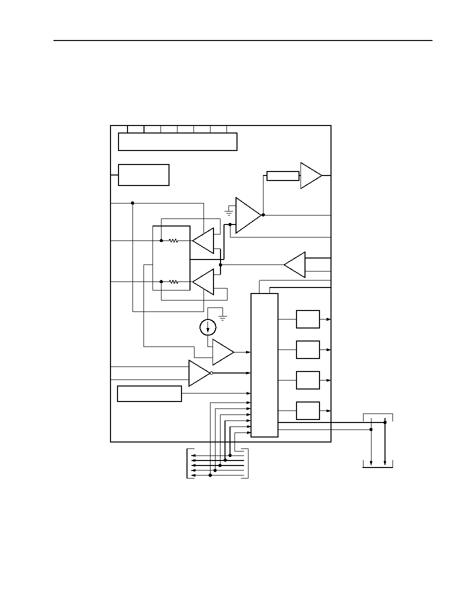
Figure 1. Functional Diagram
THERMAL
SHUTDOWN SENSE
+
≠
≠
+
≠
+
+
≠
A = 1
A = ≠1
POWER CONDITIONING & REFERENCE
CF
1
PT
PR
CURRENT
LIMIT SET
I
PROG
RTSN
RTSP
RING TRIP DETECTOR
VTX
RCVP
RCVN
NLED
RD1O
CF
2
+
+
≠
≠
TIP/RING
CURRENT
SENSE
TG
RECTIFIER
PWR
LED
DRIVE
RELAY
DRIVE
RELAY
DRIVE
RELAY
DRIVE
NLC
NRDET
NTSD
NSTAT
LATCHES
LOGIC
V
DD
DGND
RD2O
RD3O
V
CC
V
BA
T
2
BG
ND
V
BA
T
1
LOOP CLOSURE
DETECTOR
DC
OUT
3
1
RD3I
RD2I
RD1I
B1
B0
EN
TO
L8567
1, 2, 3*
FROM
T7507
CODEC
FROM
L8567
1, 2, 3
TO
T7507
CODEC
NTSD
NSTAT
AG
N
D
6
Lucent Technologies Inc.
Data Sheet
August 1999
People's Republic of China Applications
L8567 SLIC for
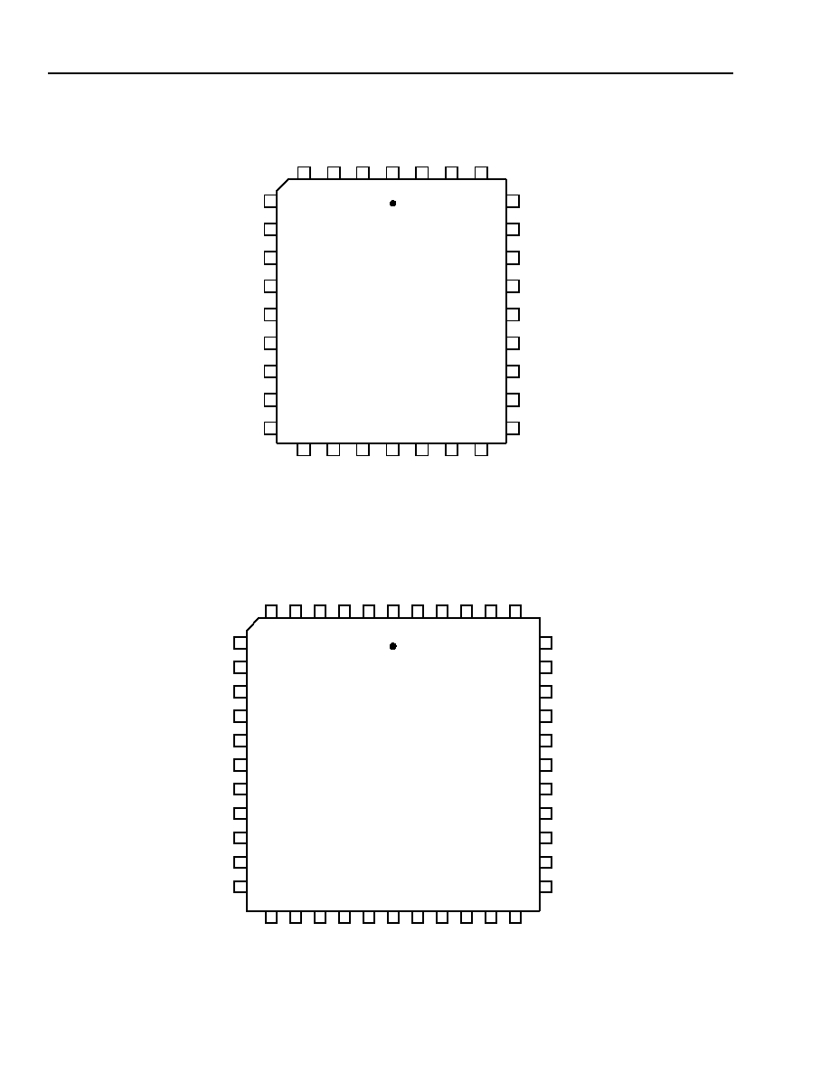
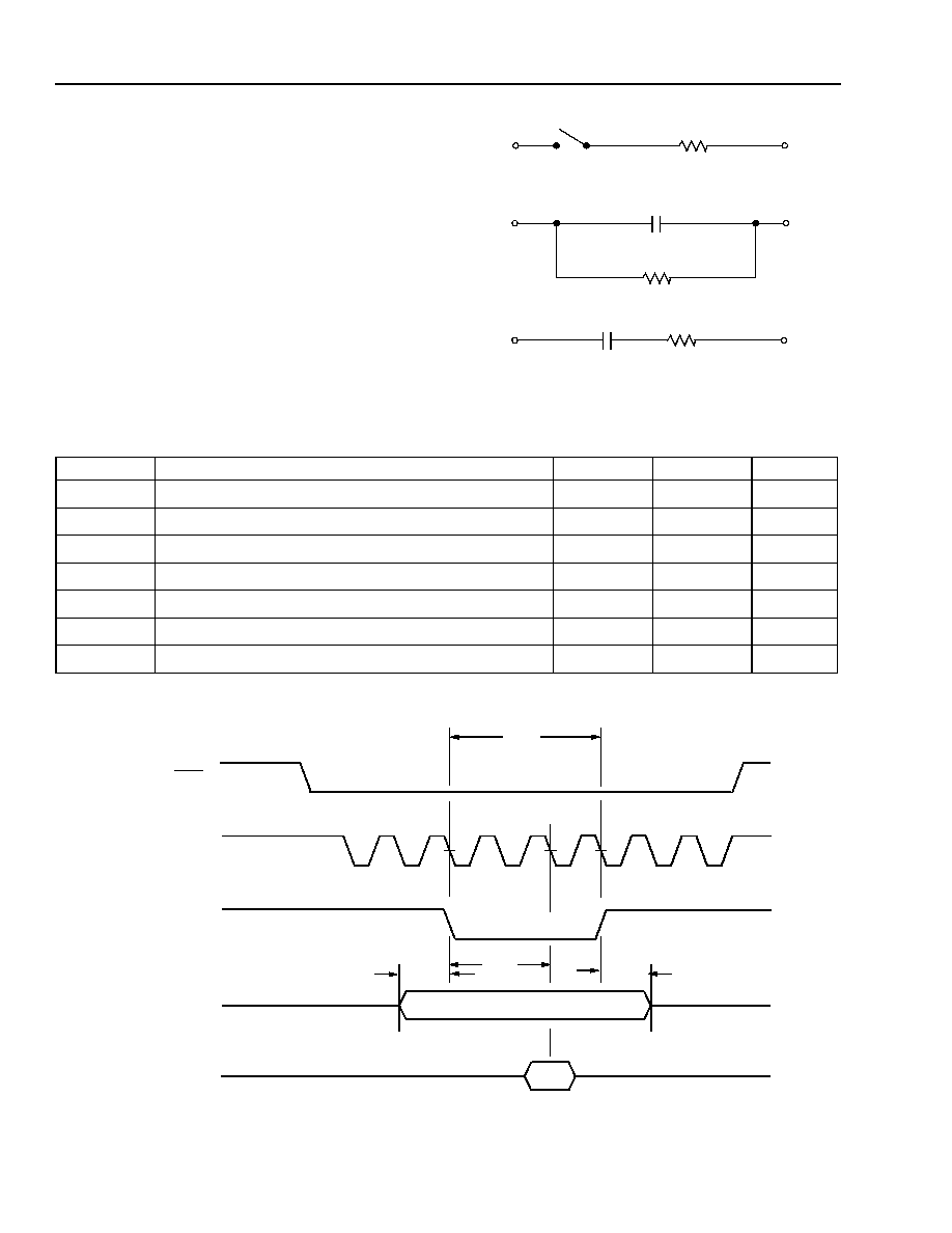
Pin Information
12-2548.i (F)
Figure 2. 32-Pin Diagram (PLCC Chip)
5-5779 (F).a
Figure 3. 44-Pin Diagram (PLCC Chip)
EN
NTSD
RCVN
AGND
VTX
TG
CF2
5
7
8
9
10
11
12
13
14
15
6
4
3
2
1
32
31
16
18
19
20
17
30
27
26
25
24
23
22
21
28
29
CF1
NLED
RD1O
RD2O
DGND
V
CC
V
DD
I
PROG
DC
OUT
RTSP
RCVP
BG
ND
R
D3O
R
D1I
R
D2I
R
D3I
B0
B1
NS
T
A
T
32-PIN PLCC
PR
PW
R
V
BA
T2
RT
S
N
PT
V
BA
T1
NC
RCVP
EN
AGND
VTX
TG
CF2
CF1
NLED
RD1O
RD2O
V
DD
V
CC
I
PROG
DC
OUT
7
9
10
11
12
13
14
15
16
17
8
6
4
3
2
1
44
43
42
41
40
5
18
20
21
22
23
24
25
26
27
28
19
39
37
36
35
34
33
32
31
30
29
38
RCVN
NC
DGND
44-PIN PLCC
PR
NC
V
BA
T
1
RD2I
RD1I
NSTAT
NC
PW
R
BG
ND
RTSN
NC
NC
NC
RT
S
P
NC
NC
PT
RD3O
B0
B1
RD3I
NC
NTSD
NC
NC
V
BA
T
2

Lucent Technologies Inc.
7
Data Sheet
August 1999
People's Republic of China Applications
L8567 SLIC for
Pin Information
(continued)
Table 1. Pin Descriptions
44-Pin
32-Pin
Symbol
Type
Description
2
1
RD3I
I
Relay Driver 3 Input. This latched logic input sets the state of the relay driv-
er number 3. When using EMRs, the relay driver is controlled by this input
via a data bus or independent data line. When using an L758X solid-state
switch, the solid-state switch is controlled directly via the data bus or inde-
pendent data line and the relay driver is unused; in this case, tie this logic
input to ground.
3
2
RD2I
I
Relay Driver 2 Input. This latched logic input sets the state of the relay driv-
er number 2. When using EMRs, the relay driver is controlled by this input
via a data bus or independent data line. When using an L758X solid-state
switch, the solid-state switch is controlled directly via the data bus or inde-
pendent data line and the relay driver is unused; in this case, tie this logic
input to ground.
4
3
RD1I
I
Relay Driver 1 Input. This latched logic input sets the state of the relay driv-
er number 1. When using EMRs, the relay driver is controlled by this input
via a data bus or independent data line. When using an L758X solid-state
switch, the solid-state switch is controlled directly via the data bus or inde-
pendent data line and the relay driver is unused; in this case, tie this logic
input to ground.
6
4
RD3O
O
Relay Driver 3 Output. Output to drive an EMR, controlled by RD3I.
5, 12,
14, 15,
20, 26,
28, 32,
35, 39,
42, 43
--
NC
--
No Connect.
7
5
RD2O
O
Relay Driver 2 Output. Output to drive an EMR, controlled by RD2I.
8
6
RD1O
O
Relay Driver 1 Output. Output to drive an EMR, controlled by RD1I.
9
7
NLED
O
NSTAT LED Driver. This output is equivalent to NSTAT, except this output
has sufficient drive capability to drive an LED. This LED driver output is an
open-collector output, so multiple outputs may be used to drive a single LED.
This output may be used as an alternative logic output to the latched NSTAT
output to indicate ring trip or loop supervision status. This output is valid re-
gardless of the state of EN.
10
8
DGND
PWR Digital Ground.
11
9
V
DD
PWR +5 V Digital Power Supply.
13
10
V
CC
PWR +5 V Analog Power Supply.
16
11
I
PROG
I
Current-Limit Program Resistor. A resistor to DC
OUT
sets the dc current
limit.
17
12
DC
OUT
O
dc Output Voltage. This output is a voltage that is directly proportional to
the absolute value of the differential tip/ring current.
18
13
RTSP
I
Ring Trip Sense Positive. Connect this pin to the ring relay and to the
ringer series through a high-value resistor.
19
14
RTSN
I
Ring Trip Sense Negative. Connect this pin to the ringing generator
through a high-value resistor.

8
Lucent Technologies Inc.
Data Sheet
August 1999
People's Republic of China Applications
L8567 SLIC for
Pin Information
(continued)
Table 1. Pin Descriptions (continued)
44-Pin 32-Pin Symbol Type
Description
21
15
PR
I/O
Protected Ring. The output of the ring driver amplifier and input to loop sensing
circuitry. Connect to loop through overcurrent series resistance.
22
16
PT
I/O
Protected Tip. The output of the tip driver amplifier and input to loop sensing cir-
cuitry. Connect to loop through overcurrent series resistance.
23
17
V
BAT1
PWR Battery Supply. Most negative primary high-voltage power supply.
24
18
BGND
PWR Battery Ground. Ground return for battery supply.
25
19
V
BAT2
PWR Auxiliary Battery Supply. Connect to the lower-voltage (magnitude) auxiliary
battery supply. If a lower-voltage auxiliary battery is not used, connect directly to
the primary high-voltage battery side.
27
20
PWR
PWR Power Control. With a 32-pin PLCC, connect a lower-voltage auxiliary battery
supply directly to PWR or connect a resistor from this node to high-voltage bat-
tery to control short-loop power dissipation. With a 44-pin PLCC, connect the
higher-voltage battery directly to PWR. Please see the Power Control section of
this data sheet for more information.
29
21
CF1
--
Filter Capacitor 1. Connect a 0.47
µ
F capacitor from this pin to CF2.
30
22
CF2
--
Filter Capacitor 2. Connect a 0.1
µ
F capacitor from this pin to AGND.
31
23
TG
I
Transmit Gain. Noninverting input to internal AX transmit amplifier. Connect a
7.87 k
resistor from this node to VTX to set internal SLIC transconductance to
39.75 V/A. Transconductance of 39.75 V/A is assumed for use with T7507
codec.
33
24
VTX
O
Transmit ac Output Voltage. Output of SLIC transmit amplifier. This output is a
voltage that is directly proportional to the differential tip/ring current. Connect a
7.87 k
resistor from this node to TG to set internal SLIC transconductance to
39.75
.
34
25
AGND
PWR Analog Signal Ground.
36
26
RCVN
I
Receive ac Signal (Inverting). This high-impedance input controls the ac differ-
ential voltage on tip and ring.
37
27
RCVP
I
Receive ac Signal (Noninverting). This high-impedance input controls the ac
differential voltage on tip and ring.
38
28
EN
I
Data Enable. Level-sensitive data latch control; when high, data at the B0, B1,
and relay driver control inputs is latched. When low, the data latch is transparent
and control signals will flow through the data latch to the SLIC control logic.
NSTAT and NTSD supervision outputs are valid only when EN is low.
40
29
NTSD
O
Not Thermal Shutdown. This gated logic output indicates if the L8567 die tem-
perature has exceeded the thermal shutdown temperature and the device has
entered the thermal shutdown mode. Input EN needs to be low for valid data to
appear at NTSD. The actual thermal shutdown is not affected by EN.
41
30
NSTAT
O
Loop Detector Output/Ring Trip Output. This gated logic output is a wired-OR
of the Not Loop Closure/Not Ring Trip detect outputs. When low, this logic output
indicates that an off-hook condition exists or that ringing has been tripped. Input
EN needs to be low for valid data to appear at NSTAT.
44
31
B1
I
State Control Input. This latched logic input, with B0, controls the state of the
SLIC.
1
32
B0
I
State Control Input. This latched logic input, with B1, controls the state of the
SLIC.

Lucent Technologies Inc.
9
Data Sheet
August 1999
People's Republic of China Applications
L8567 SLIC for
Coding Information
Table 2 shows the input state coding.
Table 2. Input State Coding
* All logic inputs are latched. The data latch is controlled by pin EN. The EN latch control is level sensitive.
When EN is high, the input data latches are active; that is, data at the B0, B1, RD1I, RD2I, and RD3I inputs are latched. The latched data will
control the state of the SLIC and drivers so that the SLIC and drivers will not respond to changes at the logic inputs while the level at EN is
high. When EN is low, the input latch is not active; therefore, data at the logic inputs will flow through the latch and immediately determine the
state of the SLIC and drivers.
If using an L758X solid-state switch, the switch is controlled directly from the T7507 codec; thus the relay drivers in the L8567 SLIC cannot be
used. If the relay drivers are not used, force them into the lowest power (not active) state by connecting RD1I, RD2I, and RD3I to ground.
B0*
B1*
RD3I* RD2I* RD1I*
State/Definition
1
1
X
X
X
Powerup, Forward Battery. Normal talk and battery feed state. Pin PT
is positive with respect to PR. On-hook transmission is enabled. The ring
trip and loop closure detectors are active.
1
0
X
X
X
Powerup, Reverse Battery. Normal talk and battery feed state. Pin PR
is positive with respect to PT. On-hook transmission is enabled. The ring
trip and loop closure detectors are active.
0
1
X
X
X
Low-Power Scan. Except for off-hook supervision, all circuits are shut
down to conserve power. Pin PT is positive with respect to PR. Thermal
shutdown is active. Note that the ring trip detector is not active during the
low-power scan. To ensure that the ring trip detector is active during ring-
ing, the L8567 SLIC must be put into the forward or reverse powerup state
before applying power ringing to the loop.
0
0
X
X
X
Disconnect. The tip and ring amplifiers are turned off and the SLIC goes
into a high-impedance (>100 k
) state. The L8567 will reset into this state
on powerup.
X
X
1
X
X
Driver RD1 Output Is Active. Input pin RD1I is high. This will activate or
place the RD1 driver output into the on state. In the on state, the driver will
supply up to 40 mA of current (at 0.6 V) to the coil of an EMR, thus acti-
vating the EMR.
X
X
0
X
X
Driver RD1 Output Is Not Active
. Input pin RD1I is low. This will place
the RD1 driver output into the off state. In the off state, the driver will not
supply current to the coil of an EMR, thus deactivating the EMR.
X
X
X
1
X
Driver RD2 Output Is Active. Input pin RD2I is high. This will activate or
place the RD2 driver output into the on state. In the on state, the driver will
supply up to 40 mA of current (at 0.6 V) to the coil of an EMR, thus acti-
vating the EMR.
X
X
X
0
X
Driver RD2 Output Is Not Active
. Input pin RD2I is low. This will place
the RD2 driver output into the off state. In the off state, the driver will not
supply current to the coil of an EMR, thus deactivating the EMR.
X
X
X
X
1
Driver RD3 Output Is Active. Input pin RD3I is high. This will activate or
place the RD3 driver output into the on state. In the on state, the driver will
supply up to 40 mA of current (at 0.6 V) to the coil of an EMR, thus acti-
vating the EMR.
X
X
X
X
0
Driver RD3 Output Is Not Active
. Input pin RD3I is low. This will place
the RD3 driver output into the off state. In the off state, the driver will not
supply current to the coil of an EMR, thus deactivating the EMR.

10
Lucent Technologies Inc.
Data Sheet
August 1999
People's Republic of China Applications
L8567 SLIC for
Coding Information
(continued)
Table 3 gives the output coding.
Table 3. Supervision Coding
* Data outputs NSTAT and NTSD are gated. In order to drive the NSTAT or NTSD outputs low, both the internal detector (i.e., an off-hook or
thermal shutdown condition, respectively, exists) and pin EN must be low.
This output is not latched; data is valid regardless of the state of EN. It can be used to drive an LED or as an alternative unlatched ring
trip/off-hook detector.
Output
State
NSTAT*
0
Off-Hook or Ring Trip. dc current greater than the typical 11 mA loop current threshold is flowing
in the subscriber loop, or the ring trip comparator has detected a dc voltage greater than the ring
trip threshold. This indicates that dc current is flowing in the loop with the ring relay set in the
power ring state. The presence of dc current in the power ring state implies that the handset is
off-hook, or that a ring trip condition exists. This is a latched output. EN must be low for data on
this output to be valid.
1
On-Hook or Not Ring Trip. dc current less than the difference of the off-hook current threshold
and loop current hysteresis is flowing, or the loop is in the power ringing state and the handset is
on-hook--no dc current has been detected. This is a latched output. EN must be low for data on
this output to be valid.
NTSD*
0
The SLIC die temperature has exceeded the thermal shutdown temperature threshold, and the
SLIC is forced into the equivalent of the disconnect state, regardless of the state of the B0 and B1
logic inputs. There is a hysteresis in the shutdown circuit, and the device will remain in thermal
shutdown until the die temperature drops below the hysteresis threshold. This is a latched output.
EN must be low for data on this output to be valid.
1
The SLIC die temperature has not exceeded the thermal shutdown temperature threshold, and
the SLIC state is set per B0 and B1 logic. This is a latched output. EN must be low for data on this
output to be valid.
NLED
0
Identical to the off-hook or ring trip state of output NSTAT. In this state, NLED can supply 10 mA
at 1.0 V, which is sufficient to drive an LED. This output is an open collector output, so multiple
NLED outputs from different devices can be used to drive a common LED. This output is not
latched, so it has valid data regardless of the state of EN. NLED can be used as an alternative to
the latched NSTAT output.
1
Identical to the on-hook or not ring trip state of the pin NSTAT.

Lucent Technologies Inc.
11
Data Sheet
August 1999
People's Republic of China Applications
L8567 SLIC for
Absolute Maximum Ratings
(T
A
= 25
∞
C)
Stresses in excess of the absolute maximum ratings can cause permanent damage to the device. These are abso-
lute stress ratings only. Functional operation of the device is not implied at these or any other conditions in excess
of those given in the operational sections of the data sheet. Exposure to absolute maximum ratings for extended
periods can adversely affect device reliability.
* Use of an auxiliary battery, V
BAT2
, whose magnitude is equal to the primary battery V
BAT1
but does not exceed the absolute maximum rating,
will not damage the chip. However, in a 32-pin PLCC, it will drive the L8567 into thermal shutdown under short-loop conditions. Use a power
resistor to node PWR.
Note: The IC can be damaged unless all ground connections are applied before, and removed after, all other connections. Furthermore, when
powering the device, the user must guarantee that no external potential creates a voltage on any pin of the device that exceeds the
device ratings. Some of the known examples of conditions that cause such potentials during powerup are 1) an inductor connected to tip
and ring can force an overvoltage on V
BAT
through the protection devices if the V
BAT
connection chatters, and 2) inductance in the V
BAT
lead could resonate with the V
BAT
filter capacitor to cause a destructive overvoltage.
Recommended Operating Conditions
Parameter
Symbol
Min
Typ
Max
Unit
+5 V Power Supply
V
CC
--
--
7.0
V
+5 V Digital Supply
V
DD
--
--
7.0
V
Battery (talking) Supplies
*
V
BAT1,
V
BAT2
--
--
≠70
V
Logic Input Voltage
--
≠0.5
--
7.0
V
Analog Input Voltage
--
≠7.0
--
7.0
V
Maximum Junction Temperature
T
J
--
--
165
∞
C
Storage Temperature Range
T
stg
≠40
--
125
∞
C
Relative Humidity Range
R
H
5
--
95
%
Ground Potential Difference (BGND to AGND)
--
--
--
±
3
V
Parameter
Min
Typ
Max
Unit
Ambient Temperature
≠40
--
85
∞
C
V
CC
Supply Voltage
4.75
5.0
5.25
V
V
DD
Supply Voltage
4.75
5.0
5.25
V
V
BAT1
Supply Voltage
≠65
≠48
≠35
V
V
BAT2
Auxiliary Battery Supply Voltage
≠35
≠24
≠15
V
dc Loop Current-limit Programming Range
15
40
45
mA
On- and Off-hook 2-wire Signal Level
--
3.17
--
dBm

12
Lucent Technologies Inc.
Data Sheet
August 1999
People's Republic of China Applications
L8567 SLIC for
Electrical Characteristics
Minimum and maximum values are testing requirements in the temperature range of 25 ∞C to 85 ∞C and battery
range of ≠35 V to ≠65 V. These minimum and maximum values are guaranteed to ≠40 ∞C based on component
simulations and design verification of samples, but devices are not tested to ≠40 ∞C in production. The test circuit
shown in Figure 6 is used unless otherwise noted. Positive currents flow into the device.
Typical values are characteristics of the device design at 25 ∞C based on engineering evaluations and are not part
of the test requirements. Supply values used for typical characterization are V
CC
= V
DD
= 5.0 V, V
BAT1
= ≠48 V,
V
BAT2
= ≠25.5 V.
Table 4. Power Supply
1. This parameter is not tested in production. It is guaranteed by design and device characterization.
2. This is the total power drawn from the power supplies. If a power resistor is not used, the total power is dissipated by the SLIC through the
package. If a power resistor is used, the power is shared by the resistor and the SLIC.
Parameter
Min
Typ
Max
Unit
Power Supply Rejection 500 Hz to 3 kHz
(See Figures 6 and 7.)
1
:
V
CC
(1 kHz)
V
BAT
(500 Hz--3 kHz)
35
45
--
--
--
--
dB
dB
Thermal Protection Shutdown (T
TSD
)
1
--
165
--
∞
C
Thermal Resistance, Junction to Ambient (
JA
) (still air)
1
:
32-pin PLCC
44-pin PLCC
--
--
60
47
--
--
∞
C/W
∞
C/W
Power Supply--Powerup, No Loop Current with On-hook Trans-
mission, Relay Drivers Off, dc Supplies at Typical Values, Use
V
BAT1
and V
BAT2
:
I
CC
+ I
DD
I
BAT1
(V
BAT1
= ≠48 V)
I
BAT2
(V
BAT2
= ≠24 V)
Quiescent Active Power Dissipation
--
--
--
--
6.0
2.25
0.45
149
6.6
2.7
0.54
180
mA
mA
mA
mW
Power Supply--Low-power Scan, Forward Battery, No Loop Cur-
rent, Relay Drivers Off, Use V
BAT1
and V
BAT2
:
I
CC
+ I
DD
I
BAT1
(V
BAT1
= ≠48 V)
I
BAT2
(V
BAT2
= ≠24 V)
Quiescent Active Power Dissipation
--
--
--
--
4.0
0.61
0.0
47
4.5
0.78
0.0
60
mA
mA
mA
mW
Power Supply--Powerup, No Loop Current with On-hook Trans-
mission, Relay Drivers Off, dc Supplies at Typical Values, Use
V
BAT1
Only:
I
CC
+ I
DD
I
BAT
(V
BAT1
= ≠48 V)
Quiescent Active Power Dissipation
2
--
--
--
6.0
2.7
160
6.6
3.46
199
mA
mA
mW
Power Supply--Low-power Scan, Forward Battery, No Loop Cur-
rent, Relay Drivers Off:
I
CC
+ I
DD
I
BAT
(V
BAT1
= ≠48 V)
Power Dissipation
2
--
--
--
4.0
0.61
47
4.5
0.78
60
mA
mA
mW

Lucent Technologies Inc.
13
Data Sheet
August 1999
People's Republic of China Applications
L8567 SLIC for
Electrical Characteristics
(continued)
Table 5. 2-Wire Port
1. This parameter is not tested in production. It is guaranteed by design and device characterization.
2. The longitudinal current is independent of dc loop current.
3. Current-limit I
LIM
is programmed by a resistor, R
PROG
, from pin I
PROG
to AGND. R
PROG
(k
) = 1.59 I
LIM
(mA).
4.
IEEE
is a registered trademark of The Institute of Electrical and Electronics Engineers, Inc.
5. Longitudinal balance of circuit card will depend on loop series resistance matching.
Table 6. Analog Pin Characteristics
Parameter
Min
Typ
Max
Unit
Tip or Ring Drive Current = dc + Longitudinal + Signal Currents
65
--
--
mA
Signal Current
1
10
--
--
mArms
Longitudinal Current Capability per Wire
1, 2
8.5
15
--
mArms
dc Loop Current Limit
3
:
R
LOOP
= 100
Programmability Range
Accuracy (18 mA < I
LIM
< 45 mA)
--
15
--
I
LIM
--
--
--
45
±
15
mA
mA
%
Powerup Open-loop Voltage Levels:
Common-mode Voltage
Differential Voltage
--
|V
BAT
+ 7.8|
V
BAT
/2
|V
BAT
+ 7.1|
--
|V
BAT
+ 6.4|
V
V
Disconnect State:
PT Resistance (V
BAT
< V
PT
< 0 V)
PR Resistance (V
BAT
< V
PR
< 0 V)
--
--
1
1
--
--
M
M
dc Feed Resistance (for I
LOOP
below current limit)
--
110
--
Loop Resistance Range (3.17 dBm overload into
200 + 680
||
0.1 µF):
I
LOOP
= 18 mA at V
BAT
= ≠48 V
1800
--
--
Longitudinal to Metallic Balance--
IEEE
4
Std. 455
(See Figure 9.)
5
:
50 Hz to 300 Hz
300 Hz to 600 Hz
600 Hz to 3400 Hz
38
48
52
--
--
--
--
--
--
dB
dB
dB
Metallic to Longitudinal Balance:
1 kHz to 3 kHz
38
--
--
dB
Parameter
Min
Typ
Max
Unit
Differential PT/PR Current Sense (DC
OUT
)
Gain (PT/PR to DC
OUT
):
Forward Battery
Reverse Battery
--
--
≠119
119
--
--
V/A
V/A
Loop Closure Detector Threshold (on-hook to off-hook at V
BAT1
= ≠ 48 V)
9
11
13
mA
Loop Closure Detector Hysteresis:
Variation
--
--
2
±0.5
--
--
mA
mA
Ring Trip Comparator:
Input Offset Voltage
--
±10
--
mV
RCVN, RCVP:
Input Impedance
Gain RCVP to PT/PR
Gain RCVN to PT/PR
--
--
--
100
2
≠2
--
--
--
k
--
--

14
Lucent Technologies Inc.
Data Sheet
August 1999
People's Republic of China Applications
L8567 SLIC for
Electrical Characteristics
(continued)
Transmit direction is tip/ring to 4-wire. Receive direction is 4-wire to tip/ring.
Table 7. ac Feed Characteristics
1. This parameter is not tested in production. It is guaranteed by design and device characterization.
Logic Interface
Table 8. Logic Inputs (B0, B1, EN, RD1I, RD2I, and RD3I) and Outputs (NSTAT and NTSD)
1. Unless otherwise specified, all logic voltages are referenced to DGND.
2. This parameter is not tested in production. It is guaranteed by design and device characterization.
Parameter
Min
Typ
Max
Unit
Total Harmonic Distortion--200 Hz to 4 kHz
1
:
Off-hook
On-hook
--
--
--
--
0.3
1.0
%
%
Transmit Gain, f = 1020 Hz (See Figure 11.); PT/PR to VTX
Transmit Gain
38.56
39.75
40.94
V/A
Receive Gain, f = 1020 Hz (See Figure 11.); RCVP/RCVN to PT/PR
Receive Gain
1.94
2
2.06
--
2-wire Idle-channel Noise (200
+ 680
||
0.1 µF termination):
Psophometric
1
C-message
3 kHz Flat
1
--
--
--
--
--
--
≠77
12
20
dBmp
dBrnC
dBrn
Transmit Idle-channel Noise:
Psophometric
1
C-message
3 kHz Flat
1
--
--
--
--
--
--
≠77
12
20
dBmp
dBrnC
dBrn
Parameter
1
Symbol
Min
Max
Unit
High-level Input Voltage
V
IH
2.4
V
DDD
V
Low-level Input Voltage
V
IL
0
0.8
V
Input Bias Current (high and low)
I
IN
--
±
50
µ
A
High-level Output Voltage (I
OUT
= ≠100
µ
A)
V
OH
V
DD
≠ 1.5
V
DD
V
Low-level Output Voltage (I
OUT
= 180
µ
A)
V
OL
0
0.4
V
Output Short-circuit Current (V
OUT
= V
DD
)
I
OSS
1
35
mA
Output Load Capacitance
2
C
OL
0
50
pF

Lucent Technologies Inc.
15
Data Sheet
August 1999
People's Republic of China Applications
L8567 SLIC for
Electrical Characteristics
(continued)
Logic Interface
(continued)
Table 9. Drivers (RD1O, RD2O, and RD3O)
1
1. The relay drivers operate using the V
DD
supply. When V
DD
is first applied to the device, the relay drivers will power up and remain in the off
state until the SLIC is configured via the data interface.
2. Unless otherwise specified, all logic voltages are referenced to DGND
.
3. This parameter is not tested in production. It is guaranteed by design and device characterization
.
Table 10. LED Driver (NLED)
1
1. NLED is an open collector output, so multiple NLED outputs may be used to drive a common LED.
2. Unless otherwise specified, all logic voltages are referenced to DGND.
3. This parameter is not tested in production. It is guaranteed by design and device characterization.
Parameter
2
Symbol
Min
Max
Unit
Off-state Output Current (V
OUT
= V
DD
)
I
OFF
--
±
200
µ
A
On-state Output Voltage (I
OUT
= 40 mA)
V
ON
0
0.60
V
On-state Output Voltage (I
OUT
= 20 mA)
V
ON
0
0.40
V
Clamp Diode Reverse Current (V
OUT
= 0)
I
R
--
±
10
µ
A
Clamp Diode On Voltage (I
OUT
= 80 mA)
V
OC
V
CC
+ 0.5
V
CC
+ 3.0
V
Turn-on Time
3
t
ON
--
10
µ
s
Turn-off Time
3
t
OFF
--
10
µ
s
Parameter
2
Symbol
Min
Max
Unit
Off-state Output Current (V
OUT
= V
DD
)
I
OFF
--
±
10
µ
A
On-state Output Voltage (I
OUT
= 10 mA)
V
ON
0
1.0
V
Turn-on Time
3
t
ON
--
10
µ
s
Turn-off Time
3
t
OFF
--
10
µ
s
16
16
Lucent Technologies Inc.
Data Sheet
August 1999
People's Republic of China Applications
L8567 SLIC for
Electrical Characteristics
(continued)
Ring Trip Requirements
s
Ringing signal:
-- Voltage, minimum 35 Vrms, maximum 100 Vrms.
-- Frequency, 17 Hz to 28 Hz.
-- Crest factor, 1.4 to 2.
s
Ringing trip:
--
100 ms (typical),
250 ms (V
BAT
= ≠33 V, loop
length = 530
).
s
Pretrip:
-- The circuits in Figure 4 will not cause ringing trip.
5-5841 (F)
Figure 4. Ring Trip Circuits
RING
RING
RING
100
10 k
8 µF
TIP
TIP
TIP
2
µ
F
200
SWITCH CLOSES < 12 ms
Table 11. Timing Requirements (DI, EN, DO, and RD), CCLK = 2.048 MHz
1. Unless otherwise specified, all times are measured from the 50% point of logic transitions.
2. This parameter is not tested in production. It is guaranteed by design and device characterization.
5-5808a
Figure 5. Timing Requirements
Symbol
Parameter
1
Min
Max
Unit
t
R
, t
F
Input Rise and Fall Time EN (10% to 90%)
2
0
75
ns
C
IN
Maximum Input Capacitance
2
--
5
pF
t
PD01
Propagation Delay EN to DO
2
0
977
ns
t
PDR
Propagation Delay EN to RD Outputs
2
0
10
µ
s
t
SDC
Minimum Setup Time from DI to EN
2
488
--
ns
t
HED
Minimum Hold Time from EN to DI
2
488
--
ns
t
WEN
Minimum Pulse Width of EN
2
1465
--
µ
s
tWEN
CCLK
EN
NSTAT/NTSD
tSDC
RD1, RD2, RD3
CSEL
B0/B1
tPD01
tHED
Lucent Technologies Inc.
17
Data Sheet
August 1999
People's Republic of China Applications
L8567 SLIC for
Test Configurations
12-2578.e (F)
Figure 6. Basic Test Circuit
NSTAT
V
BAT1
V
BAT1
BGND
V
CC
AGND
V
CC
0.1
µ
F
0.1
µ
F
PT
PR
I
PROG
DC
OUT
RTSP
RTSN
TG
RCVP
CF1
VTX
RCVN
NTSD
0.1
µ
F
CF2
R
LOOP
XMT
51.1 k
11 k
RCV
68
L8567
SLIC
TIP
RING
7.87 k
VTX
27.4 k
0.1
µ
F
PWR
0.1
µ
F
V
BAT2
B0
EN
B1
RD1O
RD2O
RD2I
RD3I
RD1I
RD3O
V
BAT2
68
63.4 k

18
18
Lucent Technologies Inc.
Data Sheet
August 1999
People's Republic of China Applications
L8567 SLIC for
Test Configurations
(continued)
PSRR = 20 log
12-2582 (F)
Figure 7. Metallic PSRR
PSRR = 20 log
12-2583 (F)
Figure 8. Longitudinal PSRR
LONGITUDINAL BALANCE = 20 log
12-2584 (F)
Figure 9. Longitudinal Balance
12-2585 (F)
Figure 10. Longitudinal Impedance
12-2587.h (F)
Figure 11. ac Gains
V
S
4.7
µ
F
100
V
BAT
OR
V
CC
DISCONNECT
V
T/R
900
V
BAT
OR V
CC
PT
PR
BASIC
TEST CIRCUIT
+
≠
CAPACITOR
BYPASS
V
S
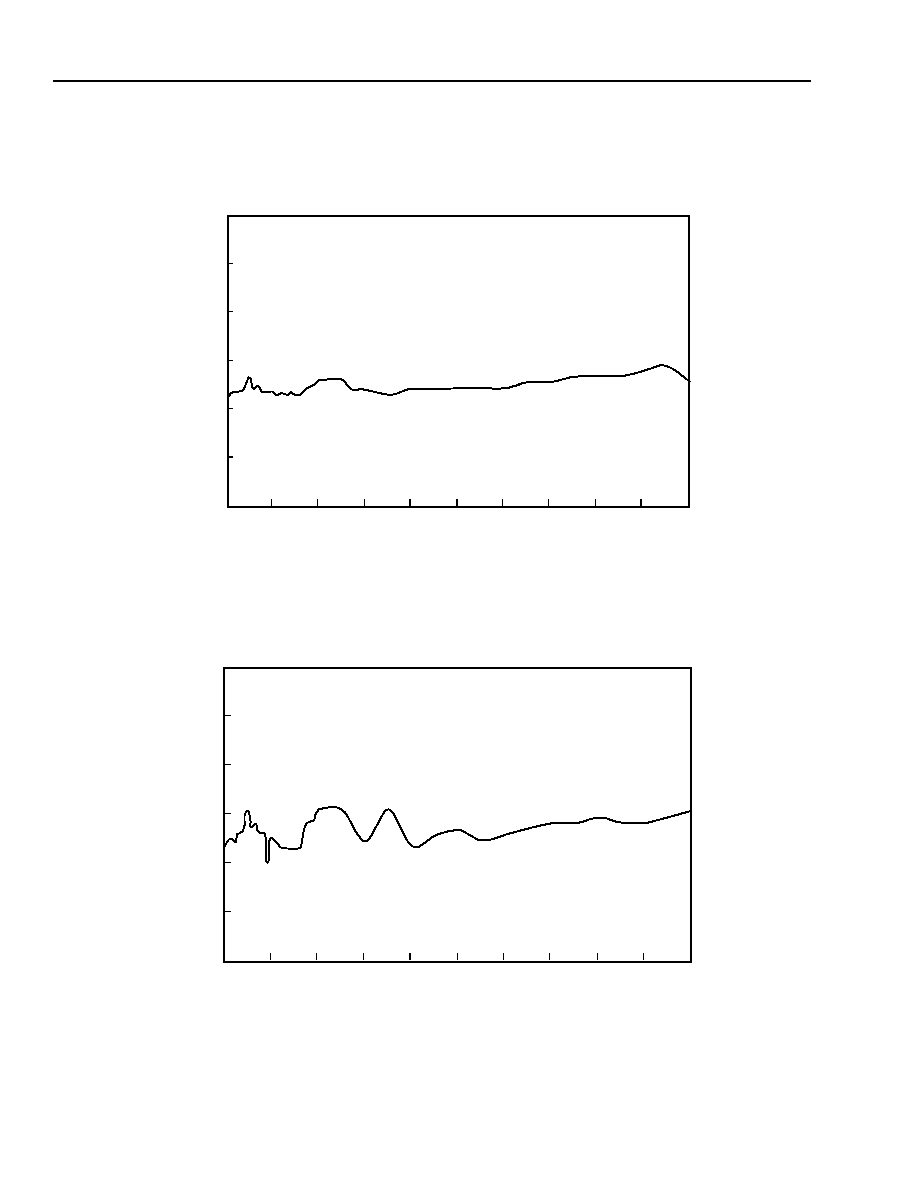
V
T/R
----------
V
S
4.7
µ
F
100
V
BAT
OR
V
CC
DISCONNECT
BYPASS
56.3
V
BAT
OR V
CC
PT
PR
BASIC
TEST CIRCUIT
67.5
10
µ
F
10
µ
F
67.5
V
M
+
≠
CAPACITOR
V
S
V
M
-------
PT
PR
BASIC
TEST CIRCUIT
365
100
µ
F
100
µ
F
365
V
M
+
≠
V
S
V
S
V
M
-------
PT
PR
BASIC
TEST CIRCUIT
+
≠
+
≠
I
LONG
I
LONG
V
PT
V
PR
Z
LONG
=
OR
V
PT
I
LONG
V
PR
I
LONG
PT
PR
BASIC
TEST CIRCUIT
680
V
T/R
+
≠
G
XMT
=
V
XMT
V
T/R
G
RCV
=
V
T/R
V
RCV
XMT
RCV
V
S
R
G
= 7.87 k
200
0.1
µ
F
TG
VTX
RCV

Lucent Technologies Inc.
19
Data Sheet
August 1999
People's Republic of China Applications
L8567 SLIC for
Test Configurations
(continued)
RFI Rejection
Figures 12--14 show the typical RFI rejection performance of the L8567 under the various conditions listed within
each figure title. The test circuit is shown below. The input signal is 100 kHz to 100 MHz, 1 Vrms and 2 Vrms, 80%
AM, with 1 kHz side tone applied using an R&S T network (CDN). This test is performed to the IEC 801-6 (1994)
specification. Note that all power supplies (V
CC
, V
DD
, V
BAT
) are bypassed to ground, as close as possible to the IC,
with 1 nF capacitors, and all grounds are shorted on the bottom of the board as close as possible to the IC. Note
that no RFI LP filter is used at tip and ring.
12-3456 (F)
*
HP
is a registered trademark of Hewlett-Packard Company.
Figure 12. RFI Rejection Test Circuit
HP
* TIMS
4935A
R&ST
NETWORK
600
L8567
HP
3580A
SPECTRUM
ANALYZER
1 k
HP
8648C
SIGNAL
GENERATOR
RING
TIP
VTX
20
Lucent Technologies Inc.
Data Sheet
August 1999
People's Republic of China Applications
L8567 SLIC for
Test Configurations
(continued)
RFI Rejection
(continued)
12-3471a (F)
Figure 13. RFI Testing, Forward Battery, 600
Loop, No Capacitor, 1 Vrms
12-3472a (F)
Figure 14. RFI Testing, Forward Battery, 600
Loop, No Capacitor, 2 Vrms
0
10
20
30
40
50
60
70
80
90
100
≠110
≠100
≠90
≠80
≠70
≠60
≠50
FREQUENCY IN MHz
600
T
E
RM
IN
AT
IO
N
(dBm
)
600
T
E
R
M
I
N
AT
IO
N (dB
m
)
0
10
20
30
40
50
60
70
80
90
100
≠110
≠100
≠90
≠80
≠70
≠60
≠50
FREQUENCY IN MHz

Lucent Technologies Inc.
21
Data Sheet
August 1999
People's Republic of China Applications
L8567 SLIC for
Functional Description
General
The L8567 is a full-feature subscriber loop interface cir-
cuit (SLIC) designed to provide the battery feed and
supervision functions to the tip/ring pair. The device
uses a current sense/voltage feed architecture. That is,
the device senses tip/ring current and supplies a pre-
cise voltage that is proportional to the tip/ring current at
the VTX output. The overall transconductance (tip/ring
current to VTX voltage gain) is set by a single external
resistor, R
TG
. The voltage at VTX is fed to the codec.
The device feeds a precise differential voltage to tip
and ring as a function of the signal voltages at the
RCVN and RCVP inputs. The codec output is con-
nected to the RCVN/RCVP SLIC inputs.
Use with T7507 Codec for Use in People's
Republic of China
The L8567 SLIC and Lucent T7507 codec together
form a matched device set designed to meet the spe-
cific MPT (Ministry of Post and Telecom) requirements
for telephony in the People's Republic of China. The ac
interface between the L8567 and the T7507 codec is
extremely simple, requiring only a single dc blocking
capacitor in the transmit direction, and a short-circuit
connection between the codec and SLIC inputs RCVN
and RCVP.
The T7507 codec has a fixed digital transmit gain stage
and two digital gain stages in the receive direction. The
choice of gain in the receive direction is user-selectable
via a bit in the serial logic input bit stream. The transmit
gain of the T7507 codec is such that when the tip/ring
to VTX transconductance of the L8567 SLIC is set to
39.75 V/A (R
TG
= 7.87 k
), the overall tip/ring to PCM
transmit gain is 0 dB into 813
. (Note that 813
is the
equivalent resistance of the PRC complex impedance
network of 200
+ 680
||
100 nF at 1000 Hz.) The
receive gains of the T7507 codec are such that the
overall PCM to tip/ring receive gain is user-selectable
to either ≠3.5 dB or ≠7.0 dB into 813
.
Note also that the T7507 codec will digitally synthesize
a termination impedance of 200
+ 680
||
100 nF. In
order to do this, the codec will assume use of 50
series protection resistors, plus the resistance of the
L758X Lucent solid-state switch on both tip and ring. If
the L758X switch is not used, the return loss perfor-
mance will degrade slightly; however, it will still meet
MPT standards. Gain flatness will not be affected; how-
ever, gain levels will shift less than 0.2 dB. To compen-
sate (if desired), the resistance of the series protection
resistor should be increased approximately 20
, to
account for the resistance of the switch.
Hybrid cancellation is also done digitally by the T7507
codec, assuming a complex hybrid balance network of
200
+ 680
||
100 nF.
The T7507 codec operates off of a single 5 V power
supply. Thus, a line card using the L8567 SLIC and
T7507 codec does not require a ≠5 V supply. Since the
T7507 is a 5 V only device, the analog input and output
of the T7507 is referenced to 2.5 V. However, the
dynamic input range of the L8567 SLIC is high enough
to accommodate ac signals referenced to 2.5 V, thus
eliminating the need for an external dc blocking capaci-
tor in the receive direction. The basic loop start sche-
matic, using an L8567 SLIC, T7507 codec, and L7583
switch, for PRC termination, is shown in Figure 20.
The control logic interface of the L8567 SLIC is
matched to the control logic of the T7507. The latched
control inputs of the L8567 are designed to be driven
by the T7507 control data outputs. The gated supervi-
sion outputs of the L8567 SLIC are designed to feed
data inputs to the T7507 codec. The T7507 codec sup-
plies the required EN pulses to the L8567 SLIC. Con-
trol data to the L8567 and supervision from the L8567
is received from, and passed to, the microcontroller at
the serial data interface in the T7507 codec. See the
T7507 data sheet for additional details.
22
22
Lucent Technologies Inc.
Data Sheet
August 1999
People's Republic of China Applications
L8567 SLIC for
Chip Set Performance Specifications
When using the T7507 codec, L8567 SLIC, L7583
solid-state switch, and 50
protection resistors, the
following line card requirements are achieved; specified
termination impedance is shown in Figure 15.
5-5324.a
Figure 15. Termination Impedance
Gain
* ≠3.5 or ≠7.0 gain mode programmable via the T7507 serial data
interface.
Gain Flatness--In Band
Gain Flatness--Out of Band--High
Frequencies
The transmit and receive directions' frequency-depen-
dent loss relative to gain at 3400 Hz is shown below.
This specification is met by using the T7507 codec,
L8567 SLIC, L7583 solid-state switch, and 50
pro-
tection resistors (200
+ 680
|| 0.1
µ
F termination).
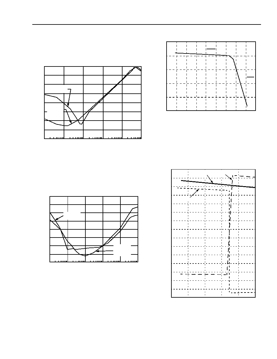
5-5340
Figure 16. Transmit and Receive Direction
Frequency-Dependent Loss Relative to
Gain at 3400 Hz
The loss for frequencies 3400 Hz < f < 4600 Hz is given
by:
b = 12.5
Gain Flatness--Out of Band--Low
Frequencies
Table 14. Gain Flatness--Out of Band--Low
Frequencies
Transmit direction only, loss relative to 1020 Hz. This
specification is met by using the T7507 codec, L8567
SLIC, L7583 solid-state switch, and 50
protection
resistors (200
+ 680
|| 0.1
µ
F termination).
Table 12. Gain
Gain @
1020 Hz
Min
Typ
Max
Unit
Transmit
≠0.7
0
+0.3
dB
Receive*
≠4.2
≠3.5
≠3.2
dB
Receive*
≠7.7
≠7.0
≠6.7
dB
Table 13. Gain Flatness--In Band
The in-band frequency-dependent loss relative to gain
at frequency = 1020 Hz, for the transmit and receive
directions. This specification is met by using the T7507
codec, L8567 SLIC, L7583 solid-state switch, and 50
protection resistors (200
+ 6800
|| 0.1
µ
F termina-
tion).
Frequency (Hz)
Min
Max
Unit
300--400
≠0.3
1.00
dB
400--600
≠0.3
0.75
dB
600--2400
≠0.3
0.35
dB
2400--3000
≠0.3
0.55
dB
3000--3400
≠0.3
1.50
dB
680
0.1
µ
F
200
Frequency (Hz)
Min Loss (dB)
16.67
30
40
26
50
30
60
30
0
≠5
10
12.5
20
25
30
LO
S
S
(dB)
3400
4000
4600
5000
ACCEPTABLE
REGION
FREQUENCY (Hz)
1
4000
f
≠
(
)
1200
-----------------------------
sin
≠
dB
Lucent Technologies Inc.
23
Data Sheet
August 1999
People's Republic of China Applications
L8567 SLIC for
Chip Set Performance Specifications
(continued)
Loss vs. Level Relative to Loss at ≠10 dBm
Input at 1020 Hz
This specification is met by using the T7507 codec,
L8567 SLIC, L7583 solid-state switch, and 50
pro-
tection resistors (200
+ 680
|| 0.1
µ
F termination).
5-5341
Figure 17. Loss vs. Level
Return Loss
The following template is achieved.
5-5325
Figure 18. Return Loss
Hybrid Balance
The following template is achieved.
5-5326
Figure 19. Hybrid Balance
+3 dBm0
≠10
≠40
≠50
≠55
1.6
0.6
0.3
0
≠0.3
≠0.6
≠1.6
LO
SS (dB
)
18
RL (dB)
14
300 500
2000
3400
FREQUENCY (Hz)
20
TB
R
L
(
d
B)
16
300 500
2500
3400
FREQUENCY (Hz)
24
Lucent Technologies Inc.
Data Sheet
August 1999
People's Republic of China Applications
L8567 SLIC for
Applications
12-3366a (F)
Figure 20. Basic Loop Start Application Using T7507 Codec and L7583 Switch for 200
+ (680
||
100 nF)
Complex Termination and Hybrid Balance
R
PR
O
G
6
3
.4 k
PW
R
DC
OU
T
I
PR
O
G
T
O
TE
ST BUS
TR
I
N
G
TL
I
N
E
T
BA
T
CR
O
W
BAR
PR
O
T
E
C
T
O
R
TI
P
RI
NG
CR
O
W
B
A
R
PR
O
T
E
C
T
O
R
R
PT
50
R
PR
50
RRING
PR
PT
RT
S
P
R
TS
P
2.
0
M
C
RT
S
2
0.2
7
µ
F
C
RT
S
1
0.
022
µ
F
R
TS
1
402
R
TS
2
274 k
R
TS
N
2.0 M
V
BA
T
V
RING
0.
1
µ
F
C
BA
T
1
BGN
D
V
BA T
1
0.
1
µ
F
C
DD
DGND
V
DD
0.1
µ
F
C
CC
V
CC
AGN
D
AGN
D
CF1
CF2
C
F1
0.47
µ
F
0.
1
µ
F
C
F2
NT
SD
NS
T
A
T
B1
B0
0.1
µ
F
C
DD
V
DD
AG
N
D
DI
CCL
K
CSEL
MC
LK
TI
M
I
N
G
AND
CONT
R
O
L
IF
S
FS
EP
SY
N
C
D
R
D
X
PC
M
HIGHW
A
Y
RCVN
RCVP
VT
X
0.1
µ
F
CB
2
R
TG
7.8
7
k
TG
L85
67 S
L
IC
1/4 T750
7
CODE
C
FG
N
D
R
BA
T
L7583
SW
I
T
C
H
RT
S
N
V
BA
T
2
VF
R
ON
VF
R
OP
VF
X
IN
TSD
IN
T
E
S
T
out
I
N
RING
IN
TE
S
T
in
LA
TC
H
V
BA
T
2
RD1
I
RD2
I
RD3
I
DO
T
O
L856
7
EN0
EN1
EN2
EN3
B0
C
B1
C
NST
A
T
C
NT
SD
C
RD1
C
RD2
C
RD3
C
NT
SD0
EN
SL
I
C
AND
L
7583
SWI
T
CH
1, 2,
OR
3
TO
L85
67
SL
I
C
1, 2
,
AND 3
FR
O
M
L8
567
SL
I
C
1,
2
,
AND 3
T
O
L
7583
B
1, 2
,
A
N
D
3
DX
EN
C
BA
T
2
0.1
µ
F
NT
S
D
1
--
3
FR
OM
L758
3B
1, 2,
A
N
D
3

Lucent Technologies Inc.
25
Data Sheet
August 1999
People's Republic of China Applications
L8567 SLIC for
Applications
(continued)
Table 15. Parts List for Loop Start Application
Name
Value
Function
Integrated Circuits
SLIC
L8567
Subscriber loop interface circuit (SLIC).
Protector
Crowbar Protector
1
1. Contact your Lucent Technologies account representative for protector recommendations. Choice of this (and all) component(s) should be
evaluated and confirmed by the customer prior to use in any field or laboratory system. Lucent does not recommend use of this part in the
field without performance verification by the customer. This device is suggested by Lucent for customer evaluation. The decision to use a
component should be based solely on customer evaluation.
Secondary protection.
Ringing and Test Access
L7583B
Switches ringing signals and test buses.
Codec
T7507
Transmit/receive gains, termination impedance, hybrid
balance, D/A, A/D, and filtering.
Overvoltage Protection
R
PT
50
Protection resistor. PTC or fusible.
R
PR
50
Protection resistor. PTC or fusible.
Power Supply
C
BAT1
/C
BAT2
0.1
µ
F, 20%, 100 V
V
BAT
filter capacitors.
C
CC
0.1
µ
F, 20%, 10 V
V
CC
filter.
C
DD
0.1
µ
F, 20%, 10 V
V
DD
filter.
C
F1
0.47
µ
F, 20%, 100 V
With C
F2
, improves idle-channel noise.
C
F2
0.1
µ
F, 20%, 100 V
With C
F1
, improves idle-channel noise.
dc Profile
R
PROG
63.4 k
, 1%, 1/16 W
Sets dc loop current limit.
R
PWR
(with single battery supply) 2.2 k
, 5%, 2 W
Limits power dissipated on the SLIC, provides dc
power to the loop.
ac Characteristics
C
B2
0.1
µ
F, 20%, 100 V
ac/dc separation capacitor.
R
TG
7.87 k
, 1%, 1/16 W
Sets SLIC transconductance.
Supervision
R
TS1
402
, 5%, 2 W
Ringing source series resistor.
R
TS2
274 k
, 1%, 1/16 W
With C
RTS2
, forms first pole of a double pole, 2 Hz ring
trip sense filter.
C
RTS1
0.022
µ
F, 20%, 5 V
With R
TSN
, R
TSP
, forms second 2 Hz filter pole.
C
RTS2
0.27
µ
F, 20%, 100 V
With R
TS2
, forms first 2 Hz filter pole.
R
TSN
2 M
, 1%, 1/16 W
With C
RTS1
, R
TSP
, forms second 2 Hz filter pole.
R
TSP
2 M
, 1%, 1/16 W
With C
RTS1
, R
TSN
, forms second 2 Hz filter pole.

26
Lucent Technologies Inc.
Data Sheet
August 1999
People's Republic of China Applications
L8567 SLIC for
Applications
(continued)
Design Considerations
Table 16 shows the design parameters of the application circuit shown in Figure 20. Components that are adjusted
to program these values are also shown.
Table 16. 200
+ 680
||
0.1
µ
µ
µ
µ
F Design Parameters
Design Parameter
Parameter Value
Components Adjusted
Loop Closure Threshold
11 mA
--
dc Loop Current Limit
40 mA
R
PROG
dc Feed Resistance
246
R
PT
, R
PR
, L7583
2-wire Signal Overload Level
3.17 dBm
--
ac Termination Impedance
200
+ 680
||
0.1
µ
F
Set via T7507
Hybrid Balance Line Impedance
200
+ 680
||
0.1
µ
F
Set via T7507
Transmit Gain
0 dB
Set via T7507
Receive Gain
≠3.5 dB/≠7.0 dB
Set via T7507
Lucent Technologies Inc.
27
Data Sheet
August 1999
People's Republic of China Applications
L8567 SLIC for
Applications
(continued)
Characteristic Curves
12-2830 (F)
Figure 21. L8567 Typical V
CC
Power Supply
Rejection
12-2871 (F)
Figure 22. L8567 Typical V
BAT
Power Supply
Rejection
12-3050.g (F)
V
BAT1
= V
BAT2
= ≠48 V.
I
LIM
= 40 mA (R
PROG
= 66.5 k
).
Figure 23. L8567 Loop Current vs. Loop Voltage
12-3470 (F)
Figure 24. L8567 Loop/Battery Current (with Battery
Switch) vs. Loop Resistance
10
100
10
5
10
6
≠80
≠70
≠20
≠10
0
FREQUENCY (Hz)
1000
10
4
≠50
≠40
≠60
≠30
PSRR (dB)
CURRENT
LIMIT
BELOW
CURRENT
LIMIT
10
100
10
5
10
6
≠80
≠70
≠20
≠10
0
FREQUENCY (Hz)
1000
10
4
≠50
≠40
≠60
≠30
P
S
RR (dB)
BELOW
CURRENT
LIMIT
CURRENT
LIMIT
LOOP CURRENT
(m
A)
0
5
10
25
0
20
30
40
50
LOOP VOLTAGE (V)
15
20
10
1
R
DC
30
45
35
40
1
10 k
0
200
0.000
0.004
0.010
R
LOOP
(
)
400
BA
TT
ERY
/
LOOP
O
U
T
P
UT
(
m
A
)
600
1000
800
0.016
I
LOOPdc
I
BAT1
I
BAT2
0.002
0.006
0.012
0.018
0.008
0.014
0.020
0.022
0.024
0.026
0.028
0.030

28
28
Lucent Technologies Inc.
Data Sheet
August 1999
People's Republic of China Applications
L8567 SLIC for
Applications
(continued)
Characteristic Curves
(continued)
12-2825.b (F)
Note: Curve is relevant only to portion of total power dissipation that
is actually dissipated on the SLIC.
Figure 25. Power Derating
Power Control
The total power drawn from the talk battery during an
off-hook state is the product of the battery voltage
times the total dc loop current, plus the SLIC quiescent
power dissipation. Note that during the on-hook state,
the power is simply the SLIC quiescent power.
P
TOTAL(off-hook)
= V
BAT
∑
I
LOOP
+ P
SLIC(quiescent)
A portion of the total power is dissipated in the sub-
scriber loop, and a portion of the total power is dissi-
pated in the SLIC itself. The loop power is used to drive
the handset and is given by:
P
LOOP
= I
2
LOOP
∑
R
LOOP
I
LOOP
is the dc loop current. In the short dc loops, the
dc loop current will be limited by the SLIC. In the case
of the L8567 SLIC, the dc loop current is determined by
external resistor R
PROG
. R
LOOP
is the sum of the actual
loop resistance (wire resistance and dc handset resis-
tance) plus any protection or other series resistance.
The active or off-hook power dissipated in the SLIC is
simply the difference of the total power drawn from the
talk battery, less the loop power, less the SLIC quies-
cent or on-hook power.
P
SLIC(active)
= P
TOTAL
≠ P
LOOP
≠ P
SLIC(on-hook)
If the active power dissipated in the SLIC is too high,
the SLIC temperature will rise above the thermal shut-
down threshold and the SLIC will be driven into a ther-
mal shutdown state. The worst case is under short dc
loops at elevated ambient temperatures. The power
dissipated on the SLIC must be controlled to avoid forc-
ing the SLIC into thermal shutdown during an active
phone conversation.
With the L8567 SLIC, short-loop power dissipation may
be controlled using several user-selectable techniques.
The first involves use of a lower-voltage auxiliary bat-
tery. This will reduce the total short-loop off-hook
power. This has the advantage of not only controlling
the SLIC temperature rise, but also minimizing total
power drawn from the talk battery.
If the user chooses not to provide an auxiliary battery,
the power dissipated by the SLIC must be controlled in
some other manner. With the L8567 SLIC, this may be
done in two ways. One technique involves the use of a
single external power control resistor. This technique
does not minimize total power dissipation; rather it con-
trols the power that it is dissipating through the SLIC
package by removing some power from the SLIC
through the resistor, thus avoiding excess temperature
rise. Because of the higher thermal impedance associ-
ated with the 32-pin PLCC, this technique may be nec-
essary with the 32-pin PLCC package option.
The other technique is simply to choose the 44-pin
PLCC package option. The thermal resistance of the
44-pin PLCC is low enough to ensure, under most con-
ditions, that the thermal shutdown temperature of the
SLIC is not exceeded. Power dissipation calculations
should be made to assess design margin.
For the three configurations discussed above, connec-
tions to the V
BAT1
, V
BAT2
, and PWR nodes are outlined
in the table below.
Table 17. Power Connections
AMBIENT TEMPERATURE, T
A
(
∞
C)
20
40
60
140
180
0
500
1000
1500
2000
80
100
120
160
PO
W
E
R
(m
W
)
32 PLCC
STILL AIR 47
∞
C/W
44 PLCC
Option
Connections to Power Mode
V
BAT1
V
BAT2
PWR
32 PLCC with auxil-
iary battery
V
BAT1
V
BAT2
V
BAT2
32 PLCC with high-
voltage battery and
power resistor
V
BAT1
V
BAT1
V
BAT1
through
power
control
resistor
44 PLCC with high-
voltage battery
V
BAT1
V
BAT1
V
BAT1

Lucent Technologies Inc.
29
Data Sheet
August 1999
People's Republic of China Applications
L8567 SLIC for
Applications
(continued)
Power Control--Auxiliary Battery
With the auxiliary battery technique under long loops,
the entire L8567 draws power from the higher-voltage
battery. As the loop length decreases and the loop
current increases or limits, the final output drive stage
of the L8567 SLIC will draw power from the lower-
voltage auxiliary battery. Thus, for a given loop, with a
given loop current requirement, the minimum battery
voltage is used by the L8567 SLIC, which minimizes
the total power consumed. During on-hook or open-
circuit conditions, the high battery is seen at tip and
ring.
All circuits on the L8567, other than the final output
drive stage, are powered by the higher-voltage battery
regardless of dc loop length. Thus, SLIC quiescent
power will be determined solely by the high-voltage
battery and will not be reduced under short dc loops.
Tip/ring voltage varies as a function of loop length,
decreasing with decreasing loop length. The battery
transition will occur when the tip/ring voltage is less
than V
BAT2
by a diode drop and a V
CE(SAT)
, or about 1 V.
Thus, the transition point from V
BAT1
to V
BAT2
may be
controlled by the choice of V
BAT2
. The relationship is
given below:
V
BAT2
= T
OH
+ R
DC(TIP)
* I
LOOP
+ 2 * R
PROT
* I
LOOP
+
R
LOOP
* I
LIM
+ R
DC(RING)
* I
LIM
+ (V
DIODE +
V
CE(SAT)
)
where:
V
BAT2
= magnitude of auxiliary battery.
T
OH
= overhead voltage tip to ground, typically 2.5 V.
R
DC(TIP)
= dc feed resistance on tip, typically 55
.
I
LOOP
= loop current. V
BAT2
will switch under short-loop
conditions where it is likely that the SLIC will be current
limiting; thus, I
LOOP
= I
LIM
.
R
PROT
= series protection resistance plus L758X resis-
tance, nominal 68
.
R
LOOP
= loop resistance for transition from V
BAT1
to
V
BAT2
.
I
LIM
= SLIC current limit set per resistor R
LIM
.
R
DC(RING)
= dc feed resistance on ring, typically 55
.
(V
DIODE +
V
CE(SAT)
) = internal voltage drop associated
with battery switch circuit, typically 1 V.
Thus, the equation may be rewritten:
V
BAT2
= 2.5 V + 55 I
LIM
+ 132 I
LIM
+ R
LOOP
I
LIM
+ 55 I
LIM
+
1 V
R
LOOP
=
≠ 242
Thus, for example, for a nominal loop transition at
700
, with a 25 mA current limit, V
BAT2
should be nom-
inal 27 V.
Power Control--32-Pin PLCC with Power
Control Resistor
This section is applicable if the user chooses to use a
single high-voltage battery with an external power con-
trol resistor. The power resistor is used in conjunction
with the 32-pin PLCC package.
Resistor R
PWR
is connected from pin PWR to the bat-
tery supply. This resistor limits the power that is dissi-
pated on the SLIC. dc loop current is shared between
the SLIC and R
PWR
, thus controlling the actual power
that is dissipated on the SLIC. The value and power rat-
ing of R
PWR
is determined by the thermal capabilities of
the L8567's 32-pin PLCC package. The value and
power rating of R
PWR
is calculated as shown below.
The relationship for the power dissipated in the SLIC is
given by:
P
SLIC
= P
TOTAL
+ P
Q
≠ P
PROT
≠ P
PWR
≠ P
LOOP
(1)
Where:
P
SLIC
= the power dissipated in the SLIC.
P
TOTAL
= the total off-hook power dissipation.
P
Q
= the SLIC quiescent or on-hook power dissipation.
P
PROT
= the power dissipated in the protection resistors
(and L758X switch).
P
PWR
= the power dissipated in R
PWR
.
P
LOOP
= the power dissipated in the subscriber loop.
The relationships for the individual power dissipation
components are:
P
TOTAL
= I
LOOP
∑
|V
BAT
|
(2)
P
Q
is the active state open loop power dissipation of
the L8567 SLIC and is specified in Table 4 on page 12.
P
PROT
= (I
LOOP
)
2
∑
2R
P
(3)
P
PWR
= (4)
P
LOOP
= V
LOOP
∑
I
LOOP
(5)
Where:
I
LOOP
is the maximum dc loop current which is the dc
loop current limit that is set by resistor R
PROG
.
R
P
is the value of the protection resistor plus the resis-
tance of the L758X switch.
|V
BAT
| is the magnitude of the maximum battery volt-
age.
V
ROH
is the overhead voltage associated with the ring
lead.
V
LOOP
is the ring/tip loop voltage. This voltage is a func-
tion of the dc loop length or resistance. It will decrease
with decreasing loop resistance.
R
PWR
is the resistance of the external resistor R
PWR
.
V
BAT2
3.5
≠
I
LIM
--------------------------------
V
BAT
V
ROH
≠
V
LOO P
≠
(
)
2
R
PWR
(
)
--------------------------------------------------------------------------

30
30
Lucent Technologies Inc.
Data Sheet
August 1999
People's Republic of China Applications
L8567 SLIC for
Applications
(continued)
Power Control--32-Pin PLCC with Power
Control Resistor
(continued)
The maximum power that may be dissipated in the
SLIC
,
P
SLIC(MAX)
is given by
T
TSD
≠ T
A
= T
RISE
(6)
(7)
Where:
T
TSD
is the thermal protection shutdown temperature
and is specified in Table 4.
T
A
is the maximum ambient operating temperature.
T
RISE
is the maximum allowed SLIC temperature rise to
avoid driving the SLIC into thermal shutdown.
P
SLIC(MAX)
is the maximum allowed power that is dissi-
pated on the SLIC to avoid driving the SLIC into ther-
mal shutdown.
is the thermal resistance, junction to ambient of
the 32-pin PLCC package; it is specified in Table 4 on
page 12.
The approach to choosing the value and rating of R
PWR
follows. First use equations 6 and 7 to determine the
maximum allowed power that may be dissipated on the
SLIC without driving the SLIC into thermal shutdown.
Next consider equations 1 and 4. In both equation 1
and 4, pick a value of R
PWR
and for this value, or R
PWR
,
vary V
LOOP
from the open-circuit (on-hook) state volt-
age to the voltage seen at the minimum expected dc
loop length (100
). The idea is to use the SLIC power
dissipation value from equation 1, P
SLIC
, to ensure that
the maximum SLIC power dissipation value from equa-
tion 7, P
SLIC(MAX)
, is not exceeded for any value of loop
length. At the same time, using equation 4, try to mini-
mize the power dissipated in R
PWR
so as to choose the
minimum power rating of the resistor to minimize cost
associated with this resistor. This technique is illus-
trated in the following design example.
Power Considerations
R
PWR
Design Example:
Assume I
LOOP
= 45 mA. This assumes that a 40 mA
current limit is programmed by resistor R
PROG
set at
63.4 k
, plus a worst-case 15% tolerance that is speci-
fied in Table 5.
|V
BAT
| = 56 V.
2R
P
= 136
. This assumes use of 50
PTC in both
the tip and ring lead associated with the L7583 ON
resistance.
V
ROH
= 4 V (typical).
P
Q
= 165 mW as nominally specified in Table 4.
T
TSD
= 165
∞
C per Table 4.
T
A
= 85
∞
C.
= 60
∞
C/W per Table 4.
V
LOOP
is varied from the open-circuit voltage of approx-
imately 50 V to the voltage at a 100
loop length,
approximately 5 V.
First, using equations 6 and 7, calculate the maximum
allowed power dissipation in the SLIC.
T
TSD
≠ T
A
= T
RISE
(6)
165
∞
C ≠ 85
∞
C = 80
∞
C
(7)
P
SLIC(MAX)
=
= 1.33 W
Given the choice of R
PWR
chosen, the value of P
SLIC
in
equation 8 must be less than 1.33 W for all loop lengths
(all values of V
LOOP
in equation 1). At the same time,
R
PWR
should be chosen to minimize P
PRW
from equa-
tion 4.
Inserting values into equation 1:
P
SLIC
P
TOTAL
+ P
Q
≠ P
PROT
≠ P
PWR
≠ P
LOOP
(8)
From equation 2, 3, 4, 5
P
SLIC
I
LOOP
∑
|V
BAT
| + P
Q
≠ (I
LOOP
)
2
∑
2R
P
≠
≠ V
LOOP
∑
I
LOOP
Inserting values:
1.33 W < (0.045)(56) + 0.165 W ≠ [(0.045)
2
∑
2(50 + 18)] ≠
≠
(V
LOOP
)(0.045 mA)
(9)
P
SLIC MAX
(
)
T
RISE
JA
----------------
=
JA
JA
P
SLIC MAX
(
)
T
RISE
JA
----------------
=
80 ∞C
60 ∞C
-----------------
V
BAT
V
ROH
≠
V
LOO P
≠
(
)
2
R
PWR
--------------------------------------------------------------------------
56
4
≠
V
LOOP
≠
(
)
2
R
PWR
------------------------------------------------------

Lucent Technologies Inc.
31
Data Sheet
August 1999
People's Republic of China Applications
L8567 SLIC for
Applications
(continued)
Power Considerations
(continued)
Inserting values into equation 4:
P
PWR
=
P
PWR
=
(10)
At this point, the idea is to choose a value of R
PWR
, and
vary V
LOOP
from the on-hook value of approximately
50 V to the very short loop (~100
) value of 5 V in
both equations 9 and 10. For the choice of R
PWR
, the
relationship in equation 9 must be met to ensure that
sufficient power is dissipated in R
PWR
to ensure that
L8567 SLIC is not driven into thermal shutdown.
At the same time, for the choice of R
PWR
, equation 10
will tell what the power rating of R
PWR
needs to be.
Obviously, it is desirable to minimize P
PRW
in equation
10 to minimize the cost associated with component
R
PWR
.
An easy way to vary V
LOOP
for various values of R
PWR
is
to use a computer-based spreadsheet program.
Table 18 shows a spreadsheet for the choice of R
PWR
=
2600
. As shown, for this choice of resistor under
short loop conditions, the power dissipated in the SLIC
exceeds 1.33 W; thus, the SLIC may be driven into
thermal shutdown. Therefore, 2600
is not an appro-
priate choice of R
PWR
.
In Table 19, R
PWR
was reduced to 2200
. As shown in
this spreadsheet, under no loop conditions does the
SLIC power dissipation exceed 1.33 W. Thus, in terms
of SLIC power dissipation, 2200
is an appropriate
choice. Looking at the power dissipated in resistor
R
PWR
, the maximum power dissipation is 0.96 W, which
says a rating of 2 W (with margin) is appropriate for
2200
.
In Table 20, R
PWR
was further reduced to 1800
.
Again, with this choice, the SLIC power does not
exceed 1.33 W, so in terms of SLIC power dissipation,
1800
is also an appropriate choice. However, with
1800
, the power dissipated in R
PWR
under short loop
conditions exceeds 1 W, which suggests that for
1800
, the power rating of R
PWR
should be greater
than 2 W. Thus, while 1800
ensures the SLIC will not
be driven into thermal shutdown, because of the higher
power rating required compared to 2200
, 2200
is a
better choice.
In Table 21, R
PWR
was increased to 4400
. This is the
minimum value to get the power rating of R
PWR
to a
0.5 W resistor. However, with this choice of resistor, the
SLIC power will exceed 1.33 W; thus, 4400
is not
appropriate. This result suggests that the minimum
power rating of R
PWR
under the assumed conditions is
1 W.
Table 22 and Table 23 show results for 2200
with a
+
5% and ≠5% variation, respectively. These tables sug-
gest that a 5% tolerance is adequate for R
PWR
.
Table 18. R
PWR
= 2600
Table 19. R
PWR
= 2200
Table 20. R
PWR
= 1800
V
BAT
V
ROH
≠
V
LOO P
≠
(
)
2
R
PWR
--------------------------------------------------------------------------
56
4
≠
V
LOO P
≠
(
)
2
R
PWR
-------------------------------------------------------
P
SLIC
(W)
V
LOOP
(V)
R
PWR
(
)
P
PWR
(W)
1.334985
5
2600
0.849615
1.281138
10
2600
0.678462
1.208062
15
2600
0.526538
1.115754
20
2600
0.393846
1.004215
25
2600
0.280385
0.873446
30
2600
0.186154
0.723446
35
2600
0.111154
0.554215
40
2600
0.055385
0.365754
45
2600
0.018846
0.158062
50
2600
0.001538
P
SLIC
(W)
V
LOOP
(V)
R
PWR
(
)
P
PWR
(W)
1.180509
5
2200
1.004091
1.157782
10
2200
0.801818
1.112327
15
2200
0.622273
1.044145
20
2200
0.465455
0.953236
25
2200
0.331364
0.8396
30
2200
0.22
0.703236
35
2200
0.131364
0.544145
40
2200
0.065455
0.362327
45
2200
0.022273
0.157782
50
2200
0.001818
P
SLIC
(W)
V
LOOP
(V)
R
PWR
(
)
P
PWR
(W)
0.957378
5
1800
1.227222
0.9796
10
1800
0.98
0.974044
15
1800
0.760556
0.940711
20
1800
0.568889
0.8796
25
1800
0.405
0.790711
30
1800
0.268889
0.674044
35
1800
0.160556
0.5296
40
1800
0.08
0.357378
45
1800
0.027222
0.157378
50
1800
0.002222

32
32
Lucent Technologies Inc.
Data Sheet
August 1999
People's Republic of China Applications
L8567 SLIC for
Applications
(continued)
Power Considerations
(continued)
Table 21. R
PWR
= 4400
Table 22. R
PWR
= 2310
(R
PWR
= 2200
+ 5%)
Table 23. R
PWR
= 2090
(R
PWR
= 2200
≠ 5%)
Power Control--44-Pin PLCC Package
With the 44-pin PLCC, the thermal impedance of the
package is probably enough to ensure the SLIC ther-
mal shutdown temperature is not exceeded. Power cal-
culations, as illustrated below, should be made to
ensure design margin.
The still-air thermal resistance of the 44-pin PLCC is
47 ∞C/W; however, this number implies zero airflow as if
the L8567 were totally enclosed in a box. A more realis-
tic number would be 43 ∞C/W. This is an experimental
number that represents a thermal impedance with no
forced airflow (i.e., from a muffin fan), but from the nat-
ural airflow as seen in a typical switch cabinet.
The SLIC will enter the thermal shutdown state at typi-
cally 165 ∞C. The thermal shutdown design should
ensure that the SLIC temperature does not reach
165 ∞C under normal operating conditions.
Assume a maximum ambient operating temperature of
85 ∞C, a maximum current limit of 45 mA, and a maxi-
mum battery of ≠52 V. Further, assume a (worst case)
minimum dc loop of 100
and that 100
protection
resistors are used at both tip and ring.
1. T
TSD
≠ T
A(max)
= allowed thermal rise.
165 ∞C ≠ 85 ∞C = 80 ∞C
2. Allowed thermal rise = package thermal
impedance
∑
SLIC power dissipation.
80 ∞C = 43 ∞C/W
∑
SLIC power dissipation
SLIC power dissipation (P
D
) = 1.9 W
Thus, if the total power dissipated in the SLIC is less
than 1.9 W, it will not enter the thermal shutdown state.
Total SLIC power is calculated as:
Total P
D
= Maximum battery
∑
Maximum
current limit + SLIC quiescent power.
For the L8567, SLIC quiescent power (P
Q
) is approxi-
mated at 0.167 W. Thus,
Total P
D
= (≠52 V
∑
45 mA) + 0.167 W
Total P
D
= 2.34 W + 0.167 W
Total P
D
= 2.507 W
The power dissipated in the SLIC is the total power dis-
sipation less the power that is dissipated in the loop.
SLIC P
D
= Total power ≠ Loop power
Loop power = (I
LIM
)
2
∑
(R
dcLOOP
min + 2R
P
)
Loop power = (45 mA)
2
∑
(100
+ 200
)
Loop power = 0.61 W
SLIC power = 2.507 W ≠ 0.61 W
SLIC power = 1.897 W < 1.9 W
Thus, in this example, the thermal design ensures that
the SLIC will not enter the thermal shutdown state.
P
SLIC
(W)
V
LOOP
(V)
R
PWR
(
)
P
PWR
(W)
1.682555
5
4400
0.502045
1.558691
10
4400
0.400909
1.423464
15
4400
0.311136
1.276873
20
4400
0.232727
1.118918
25
4400
0.165682
0.9496
30
4400
0.11
0.768918
35
4400
0.065682
0.576873
40
4400
0.032727
0.373464
45
4400
0.011136
0.158691
50
4400
0.000909
P
SLIC
(W)
V
LOOP
(V)
R
PWR
(
)
P
PWR
(W)
1.228323
5
2310
0.956277
1.195964
10
2310
0.763636
1.141959
15
2310
0.592641
1.06631
20
2310
0.44329
0.969016
25
2310
0.315584
0.850076
30
2310
0.209524
0.709492
35
2310
0.125108
0.547262
40
2310
0.062338
0.363388
45
2310
0.021212
0.157868
50
2310
0.001732
P
SLIC
(W)
V
LOOP
(V)
R
PWR
(
)
P
PWR
(W)
1.127662
5
2090
1.056938
1.115581
10
2090
0.844019
1.079576
15
2090
0.655024
1.019648
20
2090
0.489952
0.935796
25
2090
0.348804
0.828021
30
2090
0.231579
0.696322
35
2090
0.138278
0.5407
40
2090
0.0689
0.361155
45
2090
0.023445
0.157686
50
2090
0.001914

Lucent Technologies Inc.
33
Data Sheet
August 1999
People's Republic of China Applications
L8567 SLIC for
dc Characteristics
The L8567 SLIC operates in a dc unbalanced mode. In
the forward active state, under open-circuit (on-hook)
conditions, the tip to ring voltage will be a nominal
7.1 V less than the battery. This is the overhead volt-
age. The tip and ring overhead is achieved by biasing
ring a nominal 4.6 V above battery and by biasing tip a
nominal 2.5 V below ground.
During off-hook conditions, some dc resistance will be
applied to the subscriber loop as a function of the phys-
ical loop length, protection, and telephone handset. As
the dc resistance decreases from infinity (on-hook) to
some finite value (off-hook), the tip to ring voltage will
decrease as shown below.
12-3431 (F)
Figure 26. Tip/Ring Voltage Decrease
As illustrated above, as loop length decreases, the tip
to ground voltage will decrease with a slope corre-
sponding to one-half the internal dc feed resistance of
the SLIC. (The L8567 dc feed resistance is a nominal
110
.) The ring to ground voltage will also decrease
with a slope corresponding to one-half the internal dc
feed resistance of the SLIC, until the SLIC reaches the
current-limit region of operation. At that point, the slope
of the ring to ground voltage will increase to the sum of
one-half the internal dc feed resistance of the SLIC
plus approximately 10 k
, which is the slope of the I/V
characteristic in the current-limit region.
The dc feed characteristic can be described by:
V
T/R
=
Where:
I
L
= dc loop current.
V
T/R
= dc loop voltage.
|V
BAT
| = battery voltage magnitude.
V
OH
= overhead voltage. This is the difference between
the battery voltage and the open loop tip/ring
voltage.
R
L
= loop resistance, not including protection resistors.
R
P
= protection resistor value.
R
dc
= SLIC internal dc feed resistance.
The design begins by drawing the desired dc template.
Refer to Figures 23, 24, and 26.
Starting from the on-hook condition and going through
to a short circuit, the curve passes through two regions:
Region 1; On-hook and low loop currents: The slope
corresponds to the dc resistance of the SLIC, R
dc1
(plus
any series resistance). The open-circuit voltage is the
battery voltage less the overhead voltage of the device,
V
OH
(7.0 V typical).
Region 2; Current limit: The dc current is limited to a val-
ue determined by external resistor R
PROG
. This region of
the dc template has a high resistance (10 k
).
Calculate the external resistor as follows:
R
PROG
(k
) = 1.59 I
LIM
(mA)
Notice that the I/V curve is uninterrupted when the
power is shifted from the high-voltage battery to the
low-voltage battery (if auxiliary battery option is used),
if the transition occurs in the current-limit region of
operation. This is shown in Figure 24.
VTIP TO GND
ON HOOK
(1/2)R
dc
BEGIN CURRENT LIMITING
(1/2)R
dc
(1/2)R
dc
+ R
LIM
DECREASING LOOP LENGTH
V
BAT
I
L
V
B A T
V
O H
≠
R
L
2R
P
R
dc
+
+
---------------------------------
=
V
BA T
V
O H
≠
(
)
R
L
◊
R
L
2R
P
R
dc
+
+
--------------------------------------------
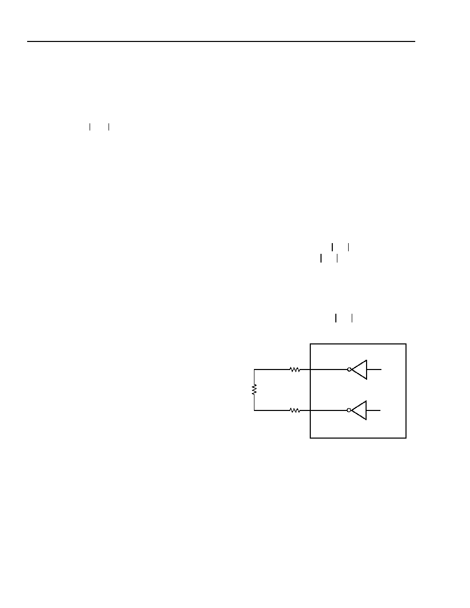
34
34
Lucent Technologies Inc.
Data Sheet
August 1999
People's Republic of China Applications
L8567 SLIC for
dc Characteristics
(continued)
Loop Range
The following equation is used to determine the dc loop
range.
Where:
R
L
= dc loop range.
|V
BAT
| = magnitude of battery voltage.
V
OH
= SLIC overhead voltage.
I
L
= dc loop current.
R
P
= series protection resistor and resistance of L758X
solid-state switch (if used).
R
dc
= SLIC dc feed resistance.
Example 1, Standard Loop:
Calculate loop range with battery voltage of 48 V, SLIC
maximum overhead of 7.8 V, SLIC dc feed resistance of
65
, 18 mA loop current requirement, worst-case
resistance of L758X switch of 28
, and 50
protec-
tion resistor with worst-case 10% tolerance of 55
.
R
L
= 1937
> 1800
Example 2, Extended Loop:
With a ≠65 V battery voltage, assuming a SLIC nominal
overhead of 7.1 V, SLIC dc feed resistance of 110
,
18 mA loop current requirement, worst-case resistance
of L758X switch of 28
, and 50
protection resistor
with worst-case 10% tolerance of 55
, what is the
maximum loop length?
dc Applications
On-Hook Transmission
In order to drive an on-hook ac signal, the SLIC must
set up the tip and ring voltage to a value less than the
battery voltage. The amount that the open loop voltage
is decreased relative to the battery is referred to as the
overhead voltage. Expressed as an equation,
V
OH
= |V
BAT
| ≠ (V
PT
≠ V
PR
)
Without this buffer voltage, amplifier saturation will
occur and the signal will be clipped. The L8567 is auto-
matically set at the factory to allow undistorted on-hook
transmission of a 3.17 dBm signal into a 900
ac loop
impedance.
The drive amplifiers are capable of 4 Vrms minimum
(V
AMP
). So, the maximum signal the device can guaran-
tee is:
The peak voltage at output of tip and ring amplifiers is
related to the peak signal voltage by:
12-2563 (F)
Figure 27. SLIC 2-Wire Output Stage
R
L
V
BAT
V
OH
≠
I
L
--------------------------------
2R
P
≠
R
dc
≠
=
R
L
48 V
7.8 V
≠
0.018 A
------------------------------------
2
55
28
+
(
)
◊
(
)
≠
130
≠
=
2941
65 V
7.1 V
≠
0.018 A
------------------------------------
2
55
28
+
(
)
◊
(
)
≠
110
≠
=
V
T/R
4 V
Z
T/R
Z
T/R
2R
P
+
--------------------------
=
Vamp =
v
T/R
1
2R
P
Z
T/R
-----------
+
≠
V
T/R
[Z
T/R
]
V
AMP
+
≠
R
P
R
P
+

Lucent Technologies Inc.
35
Data Sheet
August 1999
People's Republic of China Applications
L8567 SLIC for
dc Applications
(continued)
On-Hook Transmission
(continued)
In addition to the required peak signal level, the SLIC
needs about 2 V from each power supply to bias the
amplifier circuitry. It can be thought of as an internal
saturation voltage. Combining the saturation voltage
and the peak signal level, the required overhead can be
expressed as:
where V
SAT
is the combined internal saturation voltage
between the tip/ring amplifiers and V
BAT
(4.0 V typical).
R
P
(
) is the protection resistor value. Z
T/R
(
) is the ac
loop impedance.
Example:
Determine the required overhead to transmit on-hook
(I
LOOP
= 0) a 3.17 dBm ac signal into a 900
ac lead.
Assume use of 50
protection resistors with a 10%
tolerance or 55
and an L7583 solid-state switch. The
worst-case resistance of the switch is 28
. Note the
minimum overhead voltage of the L8567 is 6.4 V.
V
ON
= 4.0 +
3.17 dBm = 20log
Vrms = 1.296 V
V
ON
= 4.0 +
Vrms = 1.296 V
V
ON
= 4.0 +
V
OH
= 6.17 V < 6.4 V
Thus, an overhead of 6.17 V is needed for on-hook
transmission of a 3.17 dBm signal into a 900
ac load.
The L8567 has a minimum overhead of 6.4 V.
Supervision
Both the loop closure and ring trip supervision func-
tions are included on the L8567 SLIC. The outputs of
these two supervision functions are internally wired-
ORed together to form a single output NSTAT. The
wired-OR connection of the loop supervision and ring
trip detector is also available on pin NLED. This pin has
sufficient drive capability to drive an LED. This pin is an
open-collector output, so multiple pins can be used to
drive a common LED. Also included is a SLIC thermal
shutdown indicator, NTSD.
Note that the ring trip detector is not active in the low-
power scan state. The ring trip detector must be active
prior to applying power ringing to the subscriber loop.
Activate the ring trip detector by putting the L8567 SLIC
into the powerup mode before applying power ringing
to the subscriber loop.
Loop Closure
The on-hook to off-hook loop closure threshold is inter-
nally set to a nominal 11 mA at V
BAT
= ≠48 V. There is a
nominal 2 mA hysteresis. This means that the off-hook
to on-hook threshold will be a nominal 2 mA less than
the on-hook to off-hook threshold. The loop closure
threshold will track with battery voltage, increasing as
the battery gets more negative. The loop closure com-
parator has built-in longitudinal rejection, eliminating
the need for an external 50 Hz/60 Hz filter. The loop
closure detector is valid during scan, forward, and
reverse active states.
V
O H
V
SA T
1
2R
P
Z
T/R
-----------
+
v
T/R
+
=
1
2
55
28
+
[
]
◊
900
----------------------------------
+
2 V
rms
(
)
V
rms
[
]
2
900
------------------------
3
≠
10
-----------------------------
1
2
55
28
+
[
]
◊
900
----------------------------------
+
2 V
rms
(
)
1
2 55
28
+
[
]
900
----------------------------
+
2
(
)
1.296
(
)
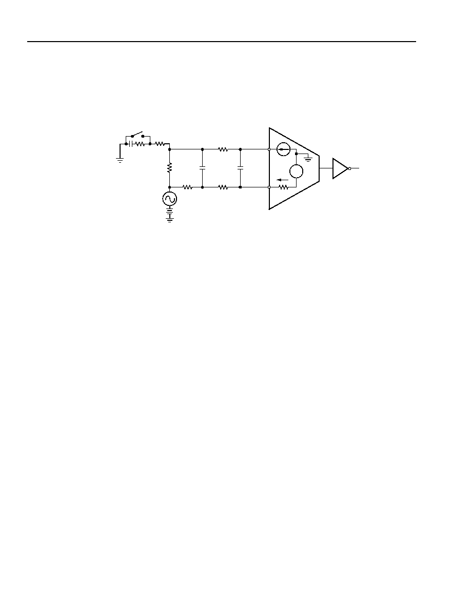
36
Lucent Technologies Inc.
Data Sheet
August 1999
People's Republic of China Applications
L8567 SLIC for
dc Applications
(continued)
Ring Trip Detection
The ring trip circuit is a comparator that has a special input section optimized for this application. The equivalent
circuit is shown in Figure 28, along with its use in an application using unbalanced, battery-backed ringing.
12-3014 (F)
Figure 28. Ring Trip Equivalent Circuit and Equivalent Application
+
≠
R
TSP
R
LOOP
15 k
7 V
I
P
= I
N
R
TSN
R
TS2
2 M
2 M
C
RTS1
0.022 µF
C
RTS2
0.27 µF
274 k
PHONE HOOK
RC PHONE
V
BAT
NRDET
R
TS1
402
RTSP
I
N
RTSN
≠
+
SWITCH
V
RING
The comparator input voltage compliance is V
CC
to
V
BAT
, and the maximum current is 240 µA in either
direction. Its application is straightforward. A resistance
(R
TSN
+ R
TS2
) in series with the R
TSN
input establishes a
current that is repeated in the R
TSP
input. A slightly
lower resistance (R
TSP
) is placed in series with the R
TSP
input. When ringing is being injected, no dc current
flows through R
TS1
, and so the R
TSP
input is at a lower
potential than R
TSN
. When enough dc loop current
flows, the R
TSP
input voltage increases to trip the com-
parator. In Figure 28, a low-pass filter with a double
pole at 2 Hz was implemented to prevent false ring trip.
The following example illustrates how the detection cir-
cuit of Figure 28 will trip at 12.5 mA dc loop current
using a ≠48 V battery.
= 17.9 µA
The current I
N
is repeated as I
P
in the positive compar-
ator input. The voltage at comparator input R
TSP
is:
V
RTSP
= V
BAT
+ I
LOOP(dc)
x R
TS1
+ I
P
x R
TSP
Using this equation and the values in the example, the
voltage at input R
TSP
is ≠12 V during ringing injection
(I
LOOP(dc)
= 0). Input R
TSP
is, therefore, at a level of 5 V
below R
TSN
. When enough dc loop current flows
through R
TS1
to raise its dc drop to 5 V, the comparator
will trip. In this example,
= 12.5 mA
Other Supervision Functions
The L8567 has on-chip thermal shutdown circuitry. If
the silicon die temperature exceeds a nominal
165
∞
C temperature, the SLIC will sense this tempera-
ture and enter the thermal shutdown mode, regardless
of the logic inputs. The thermal shutdown mode is func-
tionally similar to the disconnect state. When the die
temperature cools, the SLIC will return to the reshut-
down state. A hysteresis is included in the thermal
shutdown mechanism.
The L8567 also has a logic input pin, NEXTSD, whose
status is transferred to the serial output data bus. This
pin may be connected to an external monitoring device.
An example is the thermal shutdown output pin of the
L7583. If the L7583 enters the thermal shutdown
mode, this is reflected in the TSD output pin of this
device. The L8567 SLIC can accept this status pin and
transfer the information on this pin to the serial output
data bus.
I
N
≠7 V ≠ (≠48 V)
2.289 M
--------------------------------------
=
I
L OOP dc
( )
5 V
402
-----------------
=
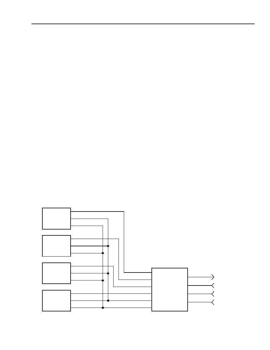
Lucent Technologies Inc.
37
Data Sheet
August 1999
People's Republic of China Applications
L8567 SLIC for
dc Applications
(continued)
Latched Parallel Data Interface
The L8567 uses a latched parallel data control scheme
for both logic inputs and logic outputs. There is a latch
enable (EN) pin associated with this control scheme.
This data control scheme is designed to work in con-
junction with the quad T7507 codec. The T7507 codec
uses a serial data interface to receive and pass control
information to and from the controlling processor. The
T7507 controls the state of the L8567 SLIC via data
inputs and outputs corresponding to those of the L8567
SLIC. The T7507 also provides the EN control signal.
The T7507 is a quad codec; that is, four channels in a
single package. Each quad codec is designed to con-
trol the four corresponding L8567 SLIC devices. Control
inputs and outputs for the four channels are shared
among the four SLICs. For example, there is only one
B0 data output from the codec, and this control signal is
passed to the B0 control input on the four associated
SLICs. There are four EN outputs from the codec, one
to each SLIC. Data on the shared input or output leads
are valid to or from a given SLIC, depending on the
state of EN pin associated with the individual SLIC.
This is shown in Figure 29 below.
The control data inputs to the SLIC are B0 and B1,
which set the state of the SLIC and RD1I, RD2I, and
RD3I, which control the state of the EMR drivers. If an
L7583 solid-state switch is used instead of EMRs, the
logic control outputs from the codec will go directly to
the state control inputs of the switch. In this mode of
operation, the relay drivers on the L8567 SLIC are not
used. If this is the case, tie the logic inputs RD1I, RD2I,
and RD3I to ground. This will force the drivers into the
not-active state, which is the state with the lowest
power consumption.
For the SLIC logic inputs, the latch is controlled by
input EN. When EN is high, the input data latches are
active; that is, data at the B0, B1, RD1I, RD2I, and
RD3I inputs are latched. The latched data will control
the state of the SLIC and drivers, and the SLIC and
drivers will not respond to changes at the logic inputs
while the level at EN is high. When EN is low, the input
data latch is not active; that is, data at the logic inputs
will flow through the latch and immediately determine
the state of the SLIC and drivers.
Logic outputs NSTAT and NTSD are also latched.
There is an internal pull-up associated with each of
these logic outputs. The operation of EN with the logic
outputs is slightly different from the operation of EN
with the logic inputs. In order for valid data to be at the
NSTAT and NTSD outputs, both the internal detector
(i.e., an off-hook or thermal shutdown condition,
respectively, exists) and pin EN must be low. Table 24
explains this.
12-3457(F)
Figure 29. Simplified Control Scheme
L8567-0
EN
B0
NSTAT
ENABLE
DATA INPUT
DATA OUTPUT
L8567-1
EN
B0
NSTAT
L8567-2
EN
B0
NSTAT
L8567-3
EN
B0
NSTAT
EN3
B0C
NSTATc
EN0
EN1
EN2
CCLK
D0
D1
CSEL
CLOCK
DATA OUT
DATA IN
CHIP SELECT
SERIAL DATA
INTERFACE TO
CONTROLLER
T7507
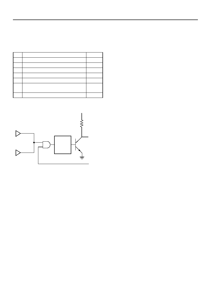
38
38
Lucent Technologies Inc.
Data Sheet
August 1999
People's Republic of China Applications
L8567 SLIC for
dc Applications
(continued)
Latched Parallel Data Interface
(continued)
Table 24. Valid Data at NSTAT and NTSD
A simplified logic output latches schematic is shown in
Figure 30.
12-3455(F)
Figure 30. Logic Output Latches
Like NSTAT, output NLED also reflects loop closure and
ring trip status. Output NLED is not latched. This output
is an open-collector output with sufficient drive capabil-
ity to drive an LED. Multiple NLED can be connected to
a common LED. NLED is valid regardless of the state
of EN. NLED can be used as an unlatched alternative
to NSTAT for control logic.
ac Design
There are four key ac design parameters. Termination
impedance is the impedance looking into the 2-wire
port of the line card. It is set to match the impedance of
the telephone loop in order to minimize echo return to
the telephone set. Transmit gain is measured from the
2-wire port to the PCM highway, while receive gain is
done from the PCM highway to the transmit port.
Finally, the hybrid balance network cancels the
unwanted amount of the receive signal that appears at
the transmit port.
First-Generation Codecs
These perform the basic filtering, A/D (transmit), D/A
(receive), and µ-law/A-law companding. They all have
an op amp in front of the A/D converter for transmit
gain setting and hybrid balance (cancellation at the
summing node). Depending on the type, some have
differential analog input stages, differential analog out-
put stages, and µ-law/A-law selectability. This genera-
tion of codecs is lower cost compared to second- and
third-generation codecs, but needs the most compli-
cated interface between the SLIC and codec. These
codecs are most suitable for applications with fixed
gains, termination impedance, and hybrid balance.
Second-Generation Codecs
This class of devices includes a microprocessor inter-
face for software control of the gains and hybrid bal-
ance. The hybrid balance is included in the device. ac
programmability adds application flexibility and saves
several passive components and also adds several I/O
latches that are needed in the application. However,
there is no transmit op amp, since the transmit gain and
hybrid balance are set internally.
Third-Generation Codecs
This class of devices includes the gains, termination
impedance, and hybrid balance--all under micropro-
cessor control. Depending on the device, it may or may
not include latches. This generation of codec offers a
very simple SLIC-codec interface with a minimal num-
ber of external components.
T7507 Codec
The T7507 provides third-generation codec functional-
ity without the programmability. In the T7507, ac gain,
termination impedance, and the hybrid balance net-
work are set digitally; thus, the SLIC-codec interface
requires virtually no external components.
However, because all the ac parameters are fixed (and
set for requirements in the PRC), the device is an
extremely cost-effective solution.
EN
State
NSTAT
0
Off-hook--loop closure or ring trip
0
0
On-hook
1
1
Don't care
1
EN
State
NTSD
0
Device in thermal shutdown
0
0
Normal operation--device state deter-
mined by B0, B1, and RD1 inputs
1
1
Don't care
1
NRDET
NLC
NSTAT
EN
CONTROL
INTERNAL
LOOP
CLOSURE
DETECTORS
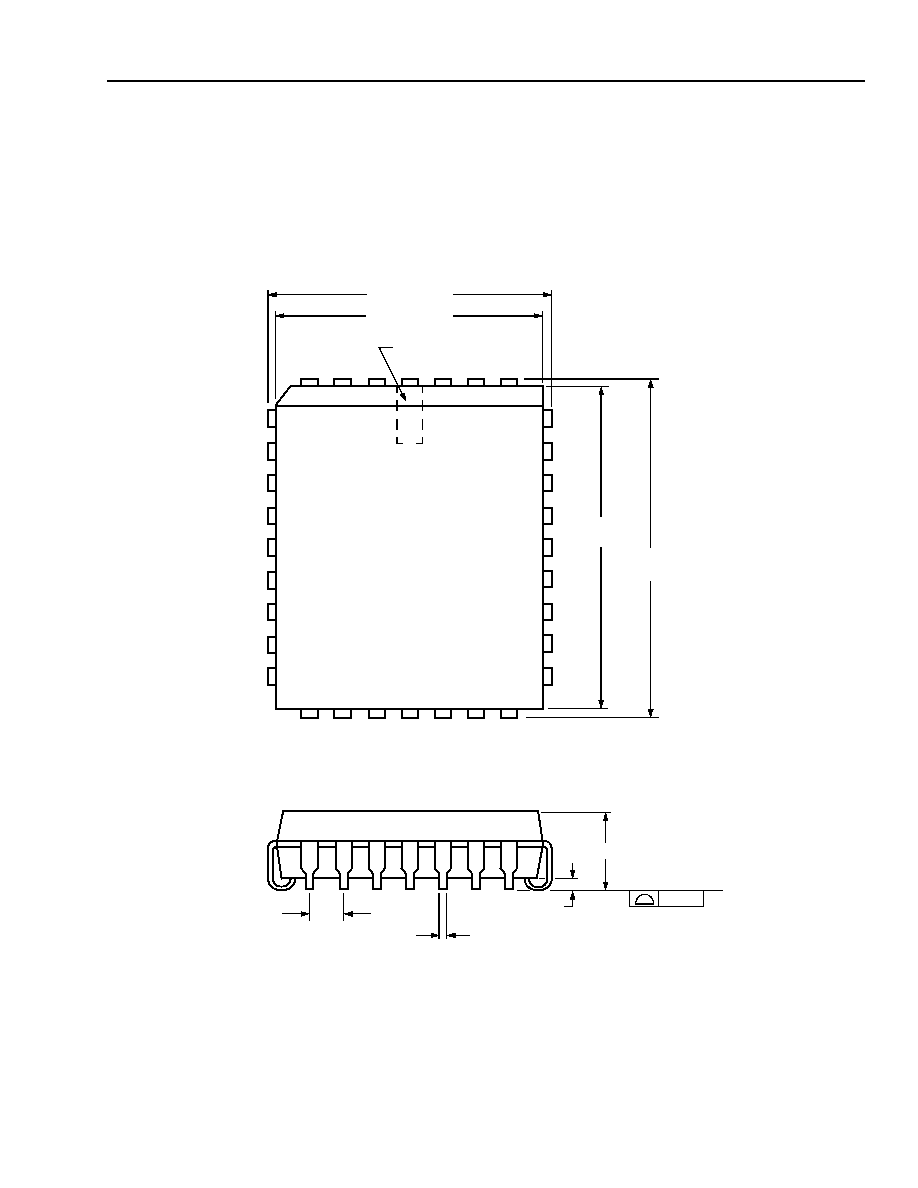
Lucent Technologies Inc.
39
Data Sheet
August 1999
People's Republic of China Applications
L8567 SLIC for
Outline Diagrams
32-Pin PLCC
Dimensions shown are metric.
Note: The dimensions in this outline diagram are intended for informational purposes only. For detailed schemat-
ics to assist your design efforts, please contact your Lucent Technologies Sales Representative.
5-3813 (F)r01
0.10
SEATING PLANE
0.38 MIN
TYP
1.27 TYP
0.330/0.533
1
4
30
5
13
21
29
14
20
12.446
±
0.127
11.430
±
0.076
PIN #1 IDENTIFIER
ZONE
14.986
±
0.127
13.970
±
0.076
3.175/3.556
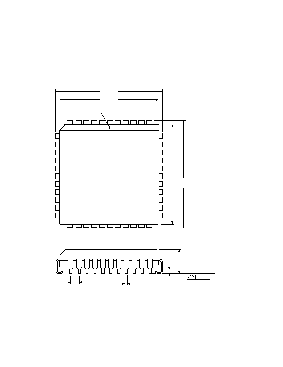
40
Lucent Technologies Inc.
Data Sheet
August 1999
People's Republic of China Applications
L8567 SLIC for
Outline Diagrams
(continued)
44-Pin PLCC
Dimensions shown are metric.
Note: The dimensions in this outline diagram are intended for informational purposes only. For detailed schemat-
ics to assist your design efforts, please contact your Lucent Technologies Sales Representative.
5-2506 (F) r07
4.57
MAX
1.27 TYP
0.53
MAX
0.10
SEATING PLANE
0.51 MIN
TYP
1
6
40
7
17
29
39
18
28
PIN #1 IDENTIFIER
ZONE
16.66 MAX
17.65 MAX
16.66
MAX
17.65
MAX

Lucent Technologies Inc.
41
Data Sheet
August 1999
People's Republic of China Applications
L8567 SLIC for
Ordering Information
Device Part No.
Description
Package
Comcode
LUCL8567AAU-D
PRC SLIC
32-Pin PLCC (Dry-bagged, Tube)
107891236
LUCL8567AAU-DT
PRC SLIC
32-Pin PLCC (Dry-bagged, Tape and Reel)
107891244
LUCL8567AP-D
PRC SLIC
44-Pin PLCC (Dry-bagged, Tube)
107957706
LUCL8567AP-DT
PRC SLIC
44-Pin PLCC (Dry-bagged, Tape and Reel)
107957714

Lucent Technologies Inc. reserves the right to make changes to the product(s) or information contained herein without notice. No liability is assumed as a result of their use or application. No
rights under any patent accompany the sale of any such product(s) or information.
Copyright © 1999 Lucent Technologies Inc.
All Rights Reserved
August 1999
DS99-100ALC (Replaces DS98-001ALC)
For additional information, contact your Microelectronics Group Account Manager or the following:
INTERNET: http://www.lucent.com/micro
E-MAIL: docmaster@micro.lucent.com
N. AMERICA:
Microelectronics Group, Lucent Technologies Inc., 555 Union Boulevard, Room 30L-15P-BA, Allentown, PA 18103
1-800-372-2447, FAX 610-712-4106 (In CANADA: 1-800-553-2448, FAX 610-712-4106)
ASIA PACIFIC: Microelectronics Group, Lucent Technologies Singapore Pte. Ltd., 77 Science Park Drive, #03-18 Cintech III, Singapore 118256
Tel. (65) 778 8833, FAX (65) 777 7495
CHINA: Microelectronics Group, Lucent Technologies (China) Co., Ltd., A-F2, 23/F, Zao Fong Universe Building, 1800 Zhong Shan Xi Road, Shanghai
200233 P. R. China Tel. (86) 21 6440 0468, ext. 316, FAX (86) 21 6440 0652
JAPAN: Microelectronics Group, Lucent Technologies Japan Ltd., 7-18, Higashi-Gotanda 2-chome, Shinagawa-ku, Tokyo 141, Japan
Tel. (81) 3 5421 1600, FAX (81) 3 5421 1700
EUROPE: Data Requests: MICROELECTRONICS GROUP DATALINE: Tel. (44) 7000 582 368, FAX (44) 1189 328 148
Technical Inquiries: GERMANY: (49) 89 95086 0 (Munich), UNITED KINGDOM: (44) 1344 865 900 (Ascot),
FRANCE: (33) 1 40 83 68 00 (Paris), SWEDEN: (46) 8 594 607 00 (Stockholm), FINLAND: (358) 9 4354 2800 (Helsinki),
ITALY: (39) 02 6608131 (Milan), SPAIN: (34) 1 807 1441 (Madrid)