Document Outline
- Features
- Description
- List of Tables
- Table 1. Pin Descriptions
- Table 2. Operating Conditions and Powering
- Table 3. Battery Feed, Switchhook Detectors (LCA and LCB), and Fault Detectors (FLTA and FLTB)
- Table 4. Ring-Trip Detctors (RTA, RTB, RZA, and RZB)
- Table 5. Relay Drivers (RDRA, RDTA, RDRB, RDTB, RDDA, and RDDB)
- Table 6. Analog Signal Pins
- Table 7. Transmission Characteristics
- Table 8. Logic Inputs (CLK, EN, and DI) and Outputs (DO)
- Table 9. Timing Requirements for CLK, EN, DI, and DO
- Table 10. MMC A31A8575AA Thick Film Resistor Module
- Table 11. Total Module Power Dissipation
- Table 12. Truth Table for EN and CLK
- Table 13. Output DATA Bit Definition
- Table 14. Input DATA Bit Definition
- Table 15. Truth Table for D1 and D0
- Table 16. External Components Required
- List of Figures
- Preliminary Pin Information
- Absolute Maximum Ratings
- Electrical Characteristics
- Applications
- Operating States
- Supervision
- dc Characteristics
- ac Design
- Application Diagram
- Outline Diagram
- Ordering Information
- Contact Us

Advance Data Sheet
March 1997
L8575 Dual-Resistive, Low-Cost
Subscriber Line Interface Circuit (SLIC)
Features
s
Two channels in a single package
s
Serial data interface
s
Per-channel powerdown
s
Low standby power (
65 mW per channel)
s
Integrated protection
s
No external protection device required
s
Battery noise cancellation
s
Switchhook detector
s
Ring-trip detector
s
Switchhook and ring-trip detector self-test
s
Fault detector
s
Zero ring voltage cross detection
s
Three relay drivers per channel
s
44-pin, surface-mount, plastic package (PLCC)
Description
The L8575 is a dual-resistive, low-cost subscriber
line interface circuit (SLIC) that is optimized to meet
both ITU-T recommendations and LSSGR require-
ments for 600
/900
resistive and complex imped-
ance termination applications. It interfaces the low-
voltage circuits on an analog line card to the Tip and
Ring of two subscriber loops. The L8575 does not
supply dc current to the subscriber loops--external
resistors are used for this purpose. The device is built
using a 90 V complementary bipolar (CBIC) process
and is available in a 44-pin PLCC package.

L8575
Advance Data Sheet
Dual-Resistive, Low-Cost SLIC
March 1997
2
Lucent Technologies Inc.
Table of Contents
Contents
Page
Features .................................................................................................................................................................. 1
Description ...............................................................................................................................................................1
Preliminary Pin Information ..................................................................................................................................... 5
Absolute Maximum Ratings (@ T
A
= 25
∞
C) ............................................................................................................ 8
Electrical Characteristics ......................................................................................................................................... 9
Relay Drivers ..................................................................................................................................................... 11
Transmission...................................................................................................................................................... 13
Serial Interface and Logic .................................................................................................................................. 14
Applications ........................................................................................................................................................... 16
General .............................................................................................................................................................. 16
Resistor Module................................................................................................................................................. 16
Protection .......................................................................................................................................................... 18
Tip/Ring Drivers ................................................................................................................................................. 20
Receive Interface ............................................................................................................................................... 20
Transmit Interface .............................................................................................................................................. 20
Battery Noise Cancellation ................................................................................................................................ 20
On-Hook Transmission....................................................................................................................................... 21
Self-Test............................................................................................................................................................. 21
Serial Data Interface .......................................................................................................................................... 21
Operating States.................................................................................................................................................... 24
Active State........................................................................................................................................................ 24
Test State........................................................................................................................................................... 24
Powerdown State with Relay Driver RDD Operated .......................................................................................... 24
Powerdown State............................................................................................................................................... 24
Ringing State (D2 = 1) ....................................................................................................................................... 24
Supervision............................................................................................................................................................ 25
Off-Hook Detection ............................................................................................................................................ 25
Ring-Trip Threshold ........................................................................................................................................... 25
Ring-Trip Requirements ......................................................................................................................................25
Fault Detection................................................................................................................................................... 26
Zero Voltage Current Cross ............................................................................................................................... 26
Relay Drivers ..................................................................................................................................................... 26
dc Characteristics .................................................................................................................................................. 27
I/V Characteristics ............................................................................................................................................. 27
Loop Length....................................................................................................................................................... 27
ac Design............................................................................................................................................................... 28
Codec Features and Selection Summary .......................................................................................................... 28
Design Equations .............................................................................................................................................. 29
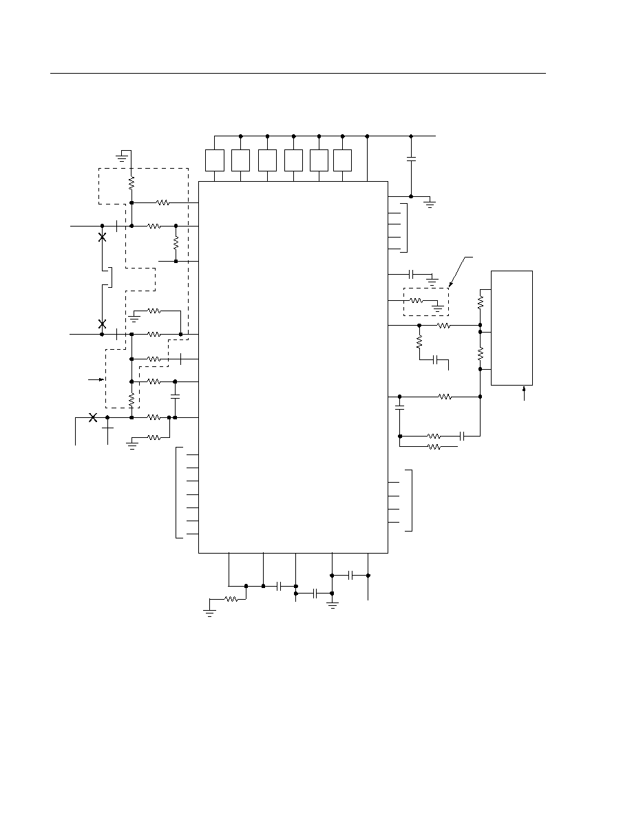
Application Diagram ..............................................................................................................................................33
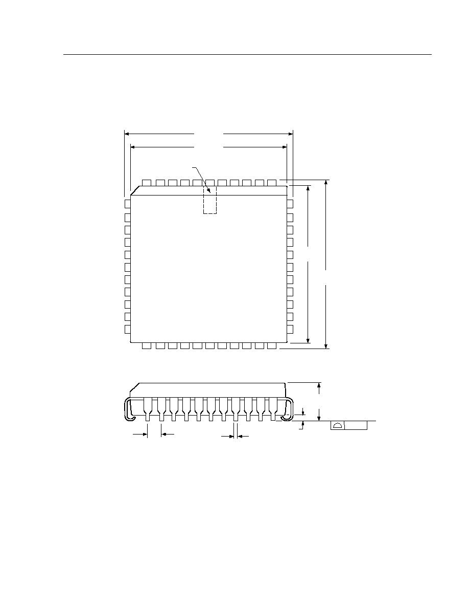
Outline Diagram..................................................................................................................................................... 35
44-Pin PLCC...................................................................................................................................................... 35
Ordering Information ..............................................................................................................................................36

Lucent Technologies Inc.
3
Advance Data Sheet
L8575
March 1997
Dual-Resistive, Low-Cost SLIC
Table of Contents
(continued)
Tables
Page
Table 1. Pin Descriptions .......................................................................................................................................... 5
Table 2. Operating Conditions and Powering ............................................................................................................9
Table 3. Battery Feed, Switchhook Detectors (LCA and LCB), and Fault Detectors (FLTA and FLTB)................... 10
Table 4. Ring-Trip Detectors (RTA, RTB, RZA, and RZB) ....................................................................................... 10
Table 5. Relay Drivers (RDRA, RDTA, RDRB, RDTB, RDDA, and RDDB)............................................................. 11
Table 6. Analog Signal Pins .................................................................................................................................... 11
Table 7. Transmission Characteristics..................................................................................................................... 13
Table 8. Logic Inputs (CLK, EN, and DI) and Outputs (DO).................................................................................... 14
Table 9. Timing Requirements for CLK, EN, DI, and DO ........................................................................................ 14
Table 10.
MMC
* A31A8575AA Thick Film Resistor Module.................................................................................... 17
Table 11. Total Module Power Dissipation .............................................................................................................. 19
Table 12. Truth Table for EN and CLK ..................................................................................................................... 22
Table 13. Output DATA Bit Definition .......................................................................................................................22
Table 14. Input DATA Bit Definition.......................................................................................................................... 23
Table 15. Truth Table for D1 and D0........................................................................................................................ 24
Table 16. External Components Required ...............................................................................................................33
Figures
Page
Figure 1. Functional Diagram ....................................................................................................................................4
Figure 2. 44-Pin PLCC Pinout .................................................................................................................................. 5
Figure 3. Power Supply Rejection vs. Frequency Diagram ..................................................................................... 15
Figure 4. L8575 SLIC Resistor Module................................................................................................................... 17
Figure 5. L8575 SLIC Dual-Resistive Matching Requirements .............................................................................. 18
Figure 6. Self-Test Mode Circuit ............................................................................................................................. 21
Figure 7. Timing Requirements for CLK, EN, DI, and DO ...................................................................................... 22
Figure 8. Logic Diagram (Positive Logic; Flip-Flops Clocked on High-to-Low Transition) ....................................... 23
Figure 9. Ring-Trip Threshold ................................................................................................................................. 25
Figure 10. Ring-Trip Circuits ...................................................................................................................................25
Figure 11. L8575 SLIC I/V Template .......................................................................................................................27
Figure 12. Equivalent Complex Terminations ..........................................................................................................29
Figure 13. Initial ac Interface for Complex Termination Between L8575 SLIC and T7504 Codec ..........................30
Figure 14. Revised ac Interface C
T
and C
R
Combined into a Single Capacitor C
S
..................................................31
Figure 15. Addition of Resistor R
SC
from XMT to IRP .............................................................................................32
Figure 16. Typical Application Diagram with Blocking Capacitors (C
B
) Included ....................................................34
*
MMC
is a registered trademark of Microelectronic Modules Corporation.

L8575
Advance Data Sheet
Dual-Resistive, Low-Cost SLIC
March 1997
4
Lucent Technologies Inc.
Description
(continued)
12-3304(F).ar1
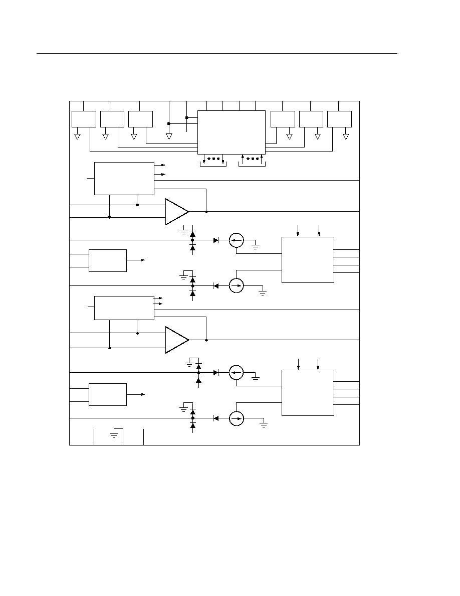
Figure 1. Functional Diagram
RELAY
DRIVER
RELAY
DRIVER
SERIAL DATA INTERFACE,
LATCHES, AND LOGIC
RELAY
DRIVER
RELAY
DRIVER
AXA
RING-TRIP
DETECTOR A
RECEIVE
INTERFACE AND
BATTERY NOISE
CANCELLATION A
≠
+
CONTROL
DETECTORS
V
BAT
SWITCHHOOK
AND
FAULT DETECTORS A
V
BAT
TIP CURRENT
SOURCE A
RING CURRENT
SOURCE A
AXB
≠
+
V
BAT
SWITCHHOOK
AND
FAULT DETECTORS B
RING-TRIP
DETECTOR B
RECEIVE
INTERFACE AND
BATTERY NOISE
CANCELLATION B
V
BAT
TIP CURRENT
SOURCE B
RING CURRENT
SOURCE B
RDDA
RDRA
DGND V
DDD
DI
DO
CLK
EN
RDTB
RDRB
TSA
RSA
PTA
RTPA
RTNA
PRA
TSB
RSB
PTB
RTPB
RTNB
PRB
RGBNB
CBNB
IRPB
VRNB
XMTB
CFLTB
RGBNA
CBNA
IRPA
VRNA
V
DDA
AGND
V
BAT
XMTA
CFLTA
NRTB
V
BAT
TSTB
PDB
V
BAT
TSTA
PDA
NRTA
NLCA
NFLTA
RELAY
DRIVER
RDRA
+5D
RELAY
DRIVER
RDDB
+5 A
V
BAT
NPLTB
NLCB

Lucent Technologies Inc.
5
Advance Data Sheet
L8575
March 1997
Dual-Resistive, Low-Cost SLIC
Preliminary Pin Information
12-3364(F)
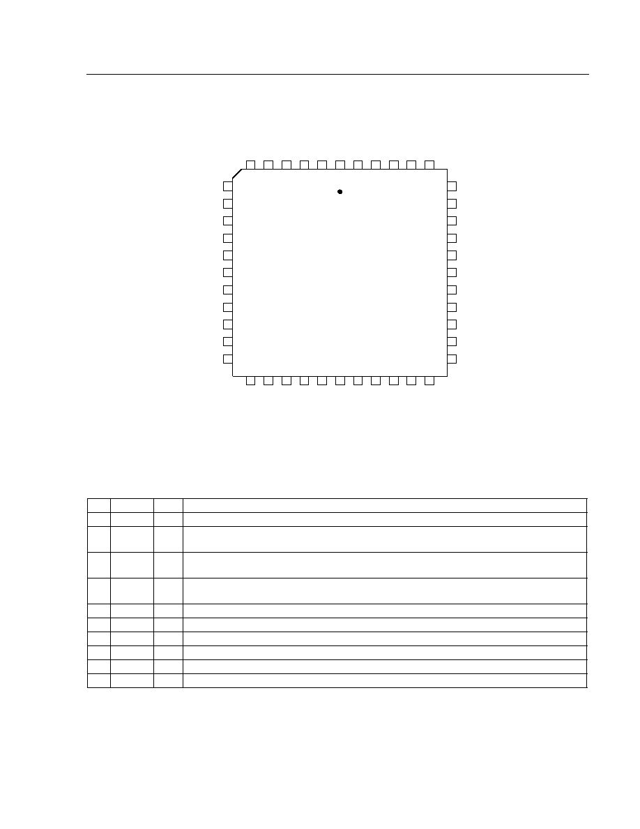
Figure 2. 44-Pin PLCC Pinout
Table 1. Pin Descriptions
Pin Symbol Type
Name/Function
1
NC
--
No Connect.
Unused pin (no internal connection).
2
DO
O
Serial Data Output.
Data in the internal 8-bit serial shift register is shifted out on this logic
output with the clock signal on pin CLK.
3
DI
I
Serial Data Input.
Data on this logic input is shifted into the 8-bit serial shift register with
the clock signal on pin CLK.
4
CFLTB
I/O
Fault Filter (Channel B).
Connect a 0.1
µ
F capacitor from CFLTB to AGND. This capaci-
tor filters Tip/Ring transients from the channel B fault detector.
5
V
DDD
--
5 V Digital dc Supply.
5 V supply for logic and relay driver flyback diodes.
6
DGND
--
Digital Ground.
Ground for channel B relay drivers.
7
RDDB
O
Disconnect Relay Driver (Channel B).
This output drives the external relay.
8
RDRB
O
Ringing Relay Driver (Channel B).
This output drives an external ringing relay.
9
RDTB
O
Test Relay Driver (Channel B).
This output drives an external test relay.
10
RTPB
I
Ring-Trip Positive (Channel B).
Positive sense input for the ring-trip detector.
RDRA
RTPA
RDTA
XMTA
TSA
RSA
RGBNA
VRNA
RTPB
RDTB
RDRB
XMTB
TSB
RSB
RGBNB
VRNB
7
9
10
11
12
13
14
15
16
17
8
6
4
3
2
1
44
43
42
41
40
5
18
20
21
22
23
24
25
26
27
28
19
39
37
36
35
34
33
32
31
30
29
38
RDDB
RTNB
RTNA
PT
A
PRA
A
GND
CBNA
CBNB
A
GND
PTB
PRB
V
DDD
DI
NC
CFL
TB
CLK
DO
EN
DGND
CFL
T
A
V
DDD
DGND
RDDA
IRPA
V
BA
T
V
DD
A
V
BA
T
IRPB
L8575

L8575
Advance Data Sheet
Dual-Resistive, Low-Cost SLIC
March 1997
6
Lucent Technologies Inc.
Preliminary Pin Information
(continued)
Table 1. Pin Descriptions
(continued)
Pin Symbol Type
Name/Function
11
RTNB
I
Ring-Trip Negative (Channel B).
Negative sense input for the ring-trip detector.
12
XMTB
O
Transmit Signal Output (Channel B).
Channel B transmit amplifier output.
13
TSB
I
Tip Sense (Channel B).
Negative input of channel B transmit op amp. Connect one high-
value resistor between TSB and the Tip of loop B and another high-value resistor between
TSB and XMTB.
14
RSB
I
Ring Sense (Channel B).
Positive input of channel B transmit op amp. Connect one high-
value resistor between RSB and the Ring of loop B and another high-value resistor between
RSB and AGND.
15
RGBNB
I
Battery Noise Gain Resistor (Channel B).
The current flowing out of PRB is 50 times the
current flowing into RGBNB. Connect a resistor from RGBNB to AGND to set the gain of the
channel B battery noise cancellation circuit.
16
VRNB
I
Receive Voltage Negative Input (Channel B).
The differential current flowing from PTB to
PRB is ≠200 times the voltage applied to VRNB, divided by the impedance connected
between IRPB and AGND.
17
IRPB
I
Receive Current Positive Input (Channel B).
The differential current flowing from PTB to
PRB is 200 times the current flowing into IRPB.
18
PTB
O
Protected Tip (Channel B).
Output of the Tip current drive amplifier B. Connect PTB to the
Tip of loop B through an overvoltage protection resistor (1.4 k
minimum).
19
PRB
O
Protected Ring (Channel B).
Output of the Ring current drive amplifier B. Connect PRB to
the Ring of loop B through an overvoltage protection resistor (1.4 k
minimum).
20
AGND
--
Analog Signal Ground.
Signal ground for channel B.
21
V
BAT
--
Office Battery Supply.
Negative office battery supply for channel B.
22
CBNB
I
Battery Noise Capacitor (Channel B).
The current flowing out of PRB is ≠50 times the
voltage applied to CBNB, divided by the impedance connected between RGBNB and
AGND. Couple V
BAT
to CBNB through a high-pass filter to eliminate battery noise from the
Tip/Ring of channel B.
23
V
DDA
--
5 V Analog dc Supply.
24
CBNA
I
Battery Noise Capacitor (Channel A).
The current flowing out of PRA is ≠50 times the
voltage applied to CBNA, divided by the impedance connected between RGBNA and
AGND. Couple V
BAT
to CBNA through a high-pass filter to eliminate battery noise from the
Tip/Ring of channel A.
25
V
BAT
--
Office Battery Supply.
Negative office battery supply for channel A.
26
AGND
--
Analog Signal Ground.
Signal ground for channel A.
27
PRA
O
Protected Ring (Channel A).
Output of the Ring current drive amplifier A. Connect PRA to
the Ring of loop A through an overvoltage protection resistor (1.4 k
minimum).
28
PTA
O
Protected Tip (Channel A).
Output of the Tip current drive amplifier A. Connect PTA to the
Tip of loop A through an overvoltage protection resistor (1.4 k
minimum).
29
IRPA
I
Receive Current Positive Input (Channel A).
The differential current flowing from PTA to
PRA is 200 times the current flowing into IRPA.
30
VRNA
I
Receive Voltage Negative Input (Channel A).
The differential current flowing from PTA to
PRA is ≠200 times the voltage applied to VRNA, divided by the impedance connected
between IRPA and AGND.

Lucent Technologies Inc.
7
Advance Data Sheet
L8575
March 1997
Dual-Resistive, Low-Cost SLIC
Preliminary Pin Information
(continued)
Table 1. Pin Descriptions
(continued)
Pin
Symbol
Type
Name/Function
31
RGBNA
I
Battery Noise Gain Resistor (Channel A).
The current flowing out of PRA is 50 times
the current flowing into RGBNA. Connect a resistor from RGBNA to AGND to set the
gain of the channel A battery noise cancellation circuit.
32
RSA
I
Ring Sense (Channel A).
Positive input of channel A transmit op amp. Connect one
high-value resistor between RSA and the Ring of loop A and another high-value resis-
tor between RSA and AGND.
33
TSA
I
Tip Sense (Channel A).
Negative input of channel A transmit op amp. Connect one
high-value resistor between TSA and the Tip of loop A and another high-value resistor
between TSA and XMTA.
34
XMTA
O
Transmit Signal Output (Channel A).
Channel A transmit amplifier output.
35
RTNA
I
Ring-Trip Negative (Channel A).
Negative sense input for the ring-trip detector.
36
RTPA
I
Ring-Trip Positive (Channel A).
Positive sense input for the ring-trip detector.
37
RDTA
O
Test Relay Driver (Channel A).
This output drives an external test relay.
38
RDRA
O
Ringing Relay Driver (Channel A).
This output drives the external ringing relay.
39
RDDA
O
Disconnect Relay Driver (Channel A).
This output drives an external relay.
40
DGND
--
Digital Ground.
Ground for channel A relay drivers.
41
V
DDD
--
5 V Digital dc Supply.
5 V supply for logic and relay driver flyback diodes.
42
CFLTA
I/O
Fault Filter (Channel A).
Connect a 0.1
µ
F capacitor from CFLTA to AGND. This
capacitor filters Tip/Ring transients from the channel A fault detector.
43
EN
I
Enable. A high-to-low transition on this logic input latches the data in the 8-bit serial
shift register into the output latches. The logic level of EN also controls which data is
shifted into the 8-bit serial shift register (refer to CLK pin description).
44
CLK
I
Clock. When the enable input (EN) is high, a low-to-high transition on this logic input
shifts data at the data input pin (DI) into the 8-bit serial shift register. When the enable
input (EN) is low, a low-to-high transition latches the states of the internal detectors into
the 8-bit serial shift register.

L8575
Advance Data Sheet
Dual-Resistive, Low-Cost SLIC
March 1997
8
Lucent Technologies Inc.
Absolute Maximum Ratings
(@ T
A
= 25
∞
C)
Stresses in excess of the absolute maximum ratings can cause permanent damage to the device. These are abso-
lute stress ratings only. Functional operation of the device is not implied at these or any other conditions in excess
of those given in the operational sections of this data sheet. Exposure to absolute maximum ratings for extended
periods can adversely affect device reliability.
Notes:
Analog and battery voltages are referenced to AGND; digital (logic) voltages are referenced to DGND.
The IC can be damaged unless all ground connections are applied before, and removed after, all other connections. Furthermore, when power-
ing the device, the user must guarantee that no external potential creates a voltage on any pin of the device that exceeds the device ratings.
Some of the known examples of conditions that cause such potentials during powering are (1) an inductor connected to Tip and Ring that can
force an overvoltage on V
BAT
through external components if the V
BAT
connection chatters, and (2) inductance in the V
BAT
lead that could reso-
nate with the V
BAT
filter capacitor to cause a destructive overvoltage.
Parameter
Symbol
Min
Value
Max
Unit
5 V Analog dc Supply
V
DDA
≠0.5
--
+7.0
V
5 V Digital dc Supply
V
DDD
≠0.5
--
+7.0
V
Office Battery Supply
V
BAT
≠65
--
+0.5
V
Logic Input Voltage
--
≠0.5
--
V
DDD
+ 0.5
V
Logic Input Clamp Diode Current, per Pin
--
--
±
20
--
mA
Logic Output Voltage
--
≠0.5
--
V
DDD
+ 0.5
V
Logic Output Current, per Pin (excluding relay drivers)
--
--
±
35
--
mA
Maximum Junction Temperature
--
--
150
--
∞
C
Operating Temperature Range
--
≠40
--
+125
∞
C
Storage Temperature Range
T
stg
≠40
--
+125
∞
C
Relative Humidity Range
--
5
--
95
%
Ground Potential Difference (DGND to AGND)
--
+0.5
--
≠0.5
V

Advance Data Sheet
L8575
March 1997
Dual-Resistive, Low-Cost SLIC
Lucent Technologies Inc.
9
Electrical Characteristics
Generally, minimum and maximum values are testing requirements. However, some parameters may not be tested
in production because they are guaranteed by design and device characterization. Typical values reflect the design
center or nominal value of the parameter; they are for information only and are not a requirement. Minimum and
maximum values apply across the entire temperature range (≠40
∞
C to +85
∞
C) and entire battery range (≠42 V to
≠58 V). Unless otherwise specified, typical values are defined as 25
∞
C, V
DDA
= 5 V, V
DDD
= 5 V, V
BAT
= ≠48 V. Posi-
tive currents flow into the device.
Table 2. Operating Conditions and Powering
1. Not to exceed 26 grams of water per kilogram of dry air.
2. Includes V
BAT
current through the external dc feed resistors, assuming the loop is open.
3. Includes power dissipation in the external dc feed resistors per application diagram, assuming the loop is open.
4. V
BAT
power supply rejection depends on the battery noise cancellation circuit. The performance stated here applies only during the active
state and assumes proper battery noise cancellation, i.e., a high-pass filter from V
BAT
to CBN and a resistor from RGBN to AGND which is 50
times the dc feed resistor connecting V
BAT
to Ring (refer to the application diagram).
5. This parameter is not tested in production. It is guaranteed by design and device characterization.
Parameter
Min
Typ
Max
Unit
Temperature Range
≠40
--
85
∞
C
Humidity Range
5
--
95
1
%RH
Supply Voltage:
V
DDA
V
DDD
V
BAT
V
DDA
≠ V
DDD
4.75
4.75
≠42
--
--
--
≠48
--
5.5
5.5
≠58
±
0.5
V
V
V
V
Supply Currents (both channels active):
I
VDDA
+ I
VDDD
(5 V)
I
VBAT
(≠48 V)
2
--
--
--
--
19.0
≠27.5
mA
mA
Supply Currents (both channels powerdown):
I
VDDA
+ I
VDDD
(5 V)
I
VBAT
(≠48 V)
2
--
--
--
--
18.0
≠2.0
mA
mA
Total Power Dissipation (5 V; ≠48 V)
3
:
Active (both channels)
Powerdown (both channels)
--
--
--
--
1.40
185
W
mW
Power-supply Rejection
4, 5
(50 mVrms ripple):
Tip/Ring and XMT
Refer to Figure 3.
Thermal
5
:
Thermal Resistance (still air)
Operating Tjc
--
--
--
--
47
155
∞
C/W
∞
C

L8575
Advance Data Sheet
Dual-Resistive, Low-Cost SLIC
March 1997
10
Lucent Technologies Inc.
Electrical Characteristics
(continued)
Table 3. Battery Feed, Switchhook Detectors (LCA and LCB), and Fault Detectors (FLTA and FLTB)
1. Assumes 2 x 300
external dc feed resistors.
2. Detector values are independent of office battery and are valid over the entire range of V
BAT
.
3. Fault voltage is defined as the absolute value of the dc voltage across either dc feed resistor. If the voltage across either feed resistor
exceeds this value, a fault is determined to be present. FLT is forced to a 0 when D2 = 1 (ringing state).
Table 4. Ring-Trip Detectors (RTA, RTB, RZA, and RZB)
1. The ringing source consists of the ac and dc voltages added together (battery-backed ringing); the ringing return is ground.
2. RT must also indicate ring-trip when the ac ringing voltage is absent (<5 Vrms) from the ringing source.
3. Pretrip: Ringing must not be tripped by a 10 k
resistor in parallel with an 8
µ
F capacitor applied across Tip and Ring.
Parameter
Min
Typ
Max
Unit
Loop Resistance Range
1
:
(3.17 dBm overload into 600
)
I
LOOP
= 18 mA at V
BAT
= ≠48 V
1800
--
--
Longitudinal Current Capability per Wire
8.5
--
--
mArms
Switchhook Detector Loop Resistance
2
:
Off-hook (LC = 1)
On-hook (LC = 0)
--
--
4800
4000
--
--
--
3200
--
Fault Detector
2, 3
:
|
V
TIP
|
or
|
V
RING
≠ V
BAT
|
No Fault (FLT = 0)
Fault (FLT = 1)
Detection Delay t
DET
(no fault to fault; CFLT = 0.1
µ
F)
Release Delay (fault to no fault; CFLT = 0.1
µ
F)
--
39
10
1.6 t
DET
36
36
--
--
33
--
30
2.5 t
DET
V
V
ms
ms
Parameter
Min
Typ
Max
Unit
Ringing Source
1
:
Frequency (
)
dc Voltage
ac Voltage
19
≠39.5
60
20
--
--
28
≠57
105
Hz
V
Vrms
Ring Trip
2, 3
(RT = 1):
Loop Resistance
Trip Time (
= 20 Hz)
RT Valid
2000
--
--
--
--
--
--
200
80
ms
ms
Ringing Source Zero Crossing (referenced to V
BAT
/2):
Ringing Voltage Positive (RZ = 1)
Ringing Voltage Negative (RZ = 0)
3V
BAT
/4
--
--
--
--
V
BAT
/4
V
V

Advance Data Sheet
L8575
March 1997
Dual-Resistive, Low-Cost SLIC
Lucent Technologies Inc.
11
Electrical Characteristics
(continued)
Relay Drivers
The relay drivers operate using the V
DDD
supply. When V
DDD
is first applied to the device, the relay drivers must
power up and remain in the off-state until the SLIC is configured via the serial data interface. The table below sum-
marizes their parameter requirements.
Table 5. Relay Drivers (RDRA, RDTA, RDRB, RDTB, RDDA, and RDDB)
1. Unless otherwise specified, all logic voltages are referenced to DGND.
2. This parameter is not tested in production. It is guaranteed by design and device characterization.
Table 6. Analog Signal Pins
1.This parameter is not tested in production. It is guaranteed by design and device characterization.
Parameter
1
Symbol
Min
Max
Unit
Off-state Output Current (V
OUT
= V
DDD
)
I
OFF
--
±
10
µ
A
On-state Output Voltage (I
OUT
= 40 mA)
V
ON
0
0.60
V
On-state Output Voltage (I
OUT
= 20 mA)
V
ON
0
0.40
V
Clamp Diode Reverse Current (V
OUT
= 0)
I
R
--
±
10
µ
A
Clamp Diode On Voltage (I
OUT
= 80 mA)
V
OC
V
DDD
+ 0.5
V
DDD
+ 3.0
V
Turn-on Time
2
t
ON
--
10
µ
s
Turn-off Time
2
t
OFF
--
10
µ
s
Parameter
Min
Typ
Max
Unit
PTA, PTB, PRA, and PRB:
Surge Current (from external source):
Continuous
1 ms Exponential Pulse (50 repetitions)
1 second, 60 Hz (60 repetitions)
10
µ
s Rectangular Pulse (10 repetitions)
--
--
--
--
--
--
--
--
±
50
±
750
±
175
±
1.25
mAdc
mA
mArms
A
Output Drive (PTA and PTB):
Drive Current (sink only)
Voltage Swing (I
OUT
= 15 mA)
dc Bias Current (active state only)
0.1
V
BAT
+ 4
5.3
--
--
5.6
15
AGND
5.9
mA
V
mA
Output Drive (PRA and PRB):
Drive Current (source only)
Voltage Swing (I
OUT
= 15 mA)
dc Bias Current (active state only)
≠15
V
BAT
≠5.3
--
--
≠5.6
≠0.1
AGND ≠ 4
≠5.9
mA
V
mA
Output Impedance (60 Hz--3.4 kHz)
1
Output Load Resistance (dc or ac)
1
1
0
--
--
--
100
M
k

L8575
Advance Data Sheet
Dual-Resistive, Low-Cost SLIC
March 1997
12
Lucent Technologies Inc.
Electrical Characteristics
(continued)
Relay Drivers
(continued)
Table 6. Analog Signal Pins (continued)
1.This parameter is not tested in production. It is guaranteed by design and device characterization.
2.A V
BAT
or ground short on XMTA or XMTB will not cause a device failure.
Parameter
Min
Typ
Max
Unit
XMTA and XMTB:
Output Drive Current
Output Voltage Swing (3 mA load):
Maximum
Minimum
±
3
V
BAT
V
BAT
+ 10
--
--
--
--
V
DDA
+2.5
mA
V
V
Output Short-circuit Current
2
Output Impedance (60 Hz--3.4 kHz)
Output Load dc Resistance
Output Load ac Impedance
1
Output Load Capacitance
1
--
--
20
2
--
--
--
--
--
--
±
30
10
--
--
50
mA
k
k
pF
VRNA and VRNB:
Input Voltage Range
Input Bias Current
Input Impedance
1
≠1.75
--
20
--
--
--
3.5
±
1
--
V
µ
A
M
IRPA and IRPB:
Input Offset Voltage (to respective VRN)
Input Impedance
--
--
--
--
±
10
5
mV
CBNA and CBNB:
Input Voltage Range
Input Bias Current
Input Impedance
≠1.75
--
50
--
--
--
3.5
±
250
--
V
nA
M
RGBNA and RGBNB:
Input Offset Voltage (to respective CBN)
Input Impedance
--
--
--
--
±
10
5
mV
TSA, TSB, RSA, and RSB:
Surge Current (from external source)
Input Voltage Range
Input Bias Current
Differential Input Impedance
1
Common-mode Input Impedance
1
External Capacitance (67 k
source impedance)
1
--
V
BAT
+ 3
--
50
50
--
--
--
--
--
--
--
±
25
AGND
±
1
--
--
10
mAdc
V
µ
A
k
M
pF

Advance Data Sheet
L8575
March 1997
Dual-Resistive, Low-Cost SLIC
Lucent Technologies Inc.
13
Electrical Characteristics
(continued)
Transmission
Transmit direction is Tip/Ring to XMT. Receive direction is IRP/VRN to Tip/Ring.
Table 7. Transmission Characteristics
1.
IEEE is a registered trademark of The Institute of Electrical and Electronics Engineers, Inc.
2. Assumes ideal external components.
3. This parameter is not tested in production. It is guaranteed by design and device characterization.
4. Transmission characteristics are specified assuming a 600
resistive termination; however, feedback using external components allows the
user to adjust the termination impedance from the intrinsic 600
of the feed resistors to most ITU-T recommended complex termination
impedances.
5. Measured with the L8575 SLIC connected per application diagram with ideal external components.
Parameter
Min
Typ
Max
Unit
Longitudinal Balance (
IEEE
1
Std. 455--1976)
2
:
50 Hz--1 kHz
1 kHz--3 kHz
54
50
70
66
--
--
dB
dB
Metallic to Longitudinal Balance
2
:
200 Hz--4 kHz
30
--
--
dB
RFI Rejection
3
:
(0.5 Vrms, 50
source, 30% AM Mod. 1 kHz)
500 kHz--10 MHz
10 MHz--100 MHz
--
--
--
--
≠65
≠45
dBV
dBV
Tip/Ring Signal Level
--
--
3.17
dBm
ac Termination Impedance
4
--
600
--
Total Harmonic Distortion (200 Hz--4 kHz)
3
--
--
0.3
%
Transmit Gain (
= 1 kHz)
5
:
Tip/Ring to XMT
≠0.486
≠0.500
≠0.514
--
Receive Gain (
= 1 kHz):
IRP Current to Differential Current Flowing from PT to PR
VRV to IRP
195
0.995
200
1
205
1.005
--
--
CBN Gain (
= 1 kHz):
1 RGBN Current to Current Flowing
CBN to RGBN
≠49.5
0.995
≠50
1
≠50.5
1.005
--
--
Gain vs. Frequency (transmit & receive; 1 kHz reference)
3
:
200 Hz--3.4 kHz
≠0.1
0
0.1
dB
Gain vs. Level (transmit & receive; 0 dBV reference)
3
:
≠50 dB to +3 dB
≠0.05
0
0.05
dB
Interchannel Crosstalk
3
:
200 Hz--3.4 kHz
--
--
77
dB
Idle-channel Noise (Tip/Ring; 600
termination):
Psophometric
3
C-message
3 kHz flat
3
--
--
--
--
--
--
≠77
12
20
dBmp
dBrnC
dBrn
Idle-channel Noise (XMT; 600
termination):
Psophometric
3
C-message
3 kHz flat
3
--
--
--
--
--
--
≠77
12
20
dBmp0
dBrnC0
dBrn0

L8575
Advance Data Sheet
Dual-Resistive, Low-Cost SLIC
March 1997
14
Lucent Technologies Inc.
Electrical Characteristics
(continued)
Serial Interface and Logic
The tables below summarize the parameter and timing requirements for logic inputs CLK, EN, DI, and DO.
Table 8. Logic Inputs (CLK, EN, and DI) and Outputs (DO)
1.
Unless otherwise specified, all logic voltages are referenced to DGND.
2.This parameter is not tested in production. It is guaranteed by design and device characterization.
Table 9. Timing Requirements for CLK, EN, DI, and DO
1.Unless otherwise specified, all times are measured from the 50% point of logic transitions.
2.This parameter is not tested in production. It is guaranteed by design and device characterization.
Parameter
1
Symbol
Min
Max
Unit
High-level Input Voltage
V
IH
2
V
DDD
V
Low-level Input Voltage
V
IL
0
0.8
V
Input Bias Current (high and low)
I
IN
--
±
50
µ
A
High-level Output Voltage (I
OUT
= ≠100
µ
A)
V
OH
V
DDD
≠ 1.5
V
DDD
V
Low-level Output Voltage (I
OUT
= 180
µ
A)
V
OL
0
0.4
V
Output Short-circuit Current (V
OUT
= V
DDD
)
I
OSS
1
35
mA
Output Load Capacitance
2
C
OL
0
50
pF
Parameter
1
Symbol
Min
Max
Unit
Input Rise and Fall Time, CLK & EN (10% to 90%)
2
t
R
, t
F
0
70
ns
Maximum Input Capacitance
2
C
IN
--
5
pF
Maximum CLK Frequency (50% duty cycle)
f
MAX
--
1.25
MHz
Propagation Delay, CLK to DO
2
t
PCO
0
350
ns
Propagation Delay, EN to RD Outputs
2
t
PCR
0
10
µ
s
Minimum Setup Time from DI to CLK
2
t
SDC
150
--
ns
Minimum Setup Time from DI to EN
2
t
SDE
150
--
ns
Minimum Setup Time from EN to CLK
2
t
SEC
150
--
ns
Minimum Hold Time from CLK to DI
2
t
HDC
50
--
ns
Minimum Hold Time from EN to CLK
2
t
HEC
50
--
ns
Minimum Pulse Width of CLK
t
WCK
400
--
ns
Minimum Pulse Width of EN
t
WEN
800
--
ns

Advance Data Sheet
L8575
March 1997
Dual-Resistive, Low-Cost SLIC
Lucent Technologies Inc.
15
Electrical Characteristics
(continued)
Serial Interface and Logic
(continued)
12-3307(F)
Figure 3. Power Supply Rejection vs. Frequency Diagram
10
1
≠40
≠30
≠20
≠10
0
FREQUENCY (Hz)
PSRR (dB)
≠50
≠60
10
2
10
3
10
4
10
5
10
6
V
DDA
(METALLIC)
V
BAT
(METALLIC)

L8575
Advance Data Sheet
Dual-Resistive, Low-Cost SLIC
March 1997
16
Lucent Technologies Inc.
Applications
General
The L8575 is a dual (channels A and B) subscriber line
interface circuit (SLIC). Each channel operates inde-
pendently such that no interaction occurs between the
channels. The following description applies to both
channels though the description may refer to only a sin-
gle channel. Some circuits, such as reference circuits
which do not impact interchannel crosstalk, are com-
mon to both channels.
The L8575 device supplies a precise differential current
to the Tip/Ring pair (via PT and PR) as a function of
analog signal voltages on IRP and VRN. However, the
current drivers connected to PT and PR are not
designed to supply dc feed current to the loop. Two
external resistors (typically 300
), connected to office
battery and ground, must be used in conjunction with
the L8575 SLIC to provide dc loop current. These resis-
tors will primarily determine the longitudinal balance of
the line feed; thus, they must be matched appropriately
to meet the longitudinal balance requirements (0.4%
for 50 dB balance).
These resistors also have a significant impact on the
termination impedance of the SLIC. Feedback, using
external components, allows the user to adjust the ter-
mination impedance from the intrinsic 600
of the feed
resistors to most ITU-T recommended complex termi-
nation impedances. Since the L8575 does not supply
dc to the loop, outputs PT and PR can be coupled to
the Tip and Ring through a resistance high enough to
allow for simple lightning protection of the drivers. How-
ever, the resistance must be low enough to achieve the
coupling of sufficient ac signals to the Tip and Ring
from the available power supply. Since the Tip and Ring
drivers are current sources, the value of the resistance
is arbitrary and does not affect the performance of the
SLIC. A minimum value of 1400
(1.4 k
)
is required
for protection purposes.
The L8575 also senses the Tip voltage, Ring voltage,
and differential Tip/Ring voltage via the TS and RS
sense inputs. The differential dc voltage is used inter-
nally for switchhook detection. The Tip and Ring volt-
ages are also used internally to detect faults on Tip and
Ring. Both detector thresholds are preset internally.
The status of each detector is monitored at pin DO by
reading the 8-bit serial shift register. The differential
Tip/Ring ac signal appears on analog output XMT.
The L8575 also includes:
s
Per-channel ring-trip detectors, loop closure detec-
tors.
s
Six relay drivers (three per channel).
s
8-bit serial-to-parallel and parallel-to-serial logic
interface.
s
Per-channel circuits which eliminate the battery
noise that is coupled to the Tip and Ring through the
dc feed resistors.
s
Fault detection.
s
Zero ring voltage detection.
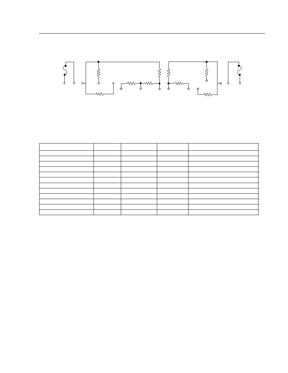
Resistor Module
The L8575 requires certain external resistors at the Tip
and Ring interface. Because of matching and protec-
tion requirements, one of the most economical options
recommended to implement these registers is in a thick
film resistor module. A schematic and a brief descrip-
tion of the function of each of these resistors is given in
Figure 4. Note that Microelectronic Modules Corpora-
tion*
MMC A31A8575AA Thick Film resistor module is
an application-specific resistor module designed for
use with the L8575 SLIC. The values, tolerance, match-
ing, and power rating of the
MMC A31A8575AA mod-
ule are given in Table 10.
Resistors R
1
and R
2
are the dc feed resistors. R
1
is
connected from battery to Ring, and R
2
is connected
from Tip to ground. The dc loop current is fed to the
subscriber loop via these resistors. These resistors will
set the dc I/V template of the line circuit with the I/V
template being linear with a ≠1/600
slope. No con-
stant current region at short dc loops is provided by
resistors R
1
and R
2
, or the L8575 SLIC.
* For additional information, contact Microelectronic Modules
Corporation (
MMC), 2601 S. Moorland Rd., New Berlin, WI 53151:
U.S.A: (414) 785-6506
FAX Number: (414) 785-6516

Advance Data Sheet
L8575
March 1997
Dual-Resistive, Low-Cost SLIC
Lucent Technologies Inc.
17
Applications
(continued)
Resistor Module
(continued)
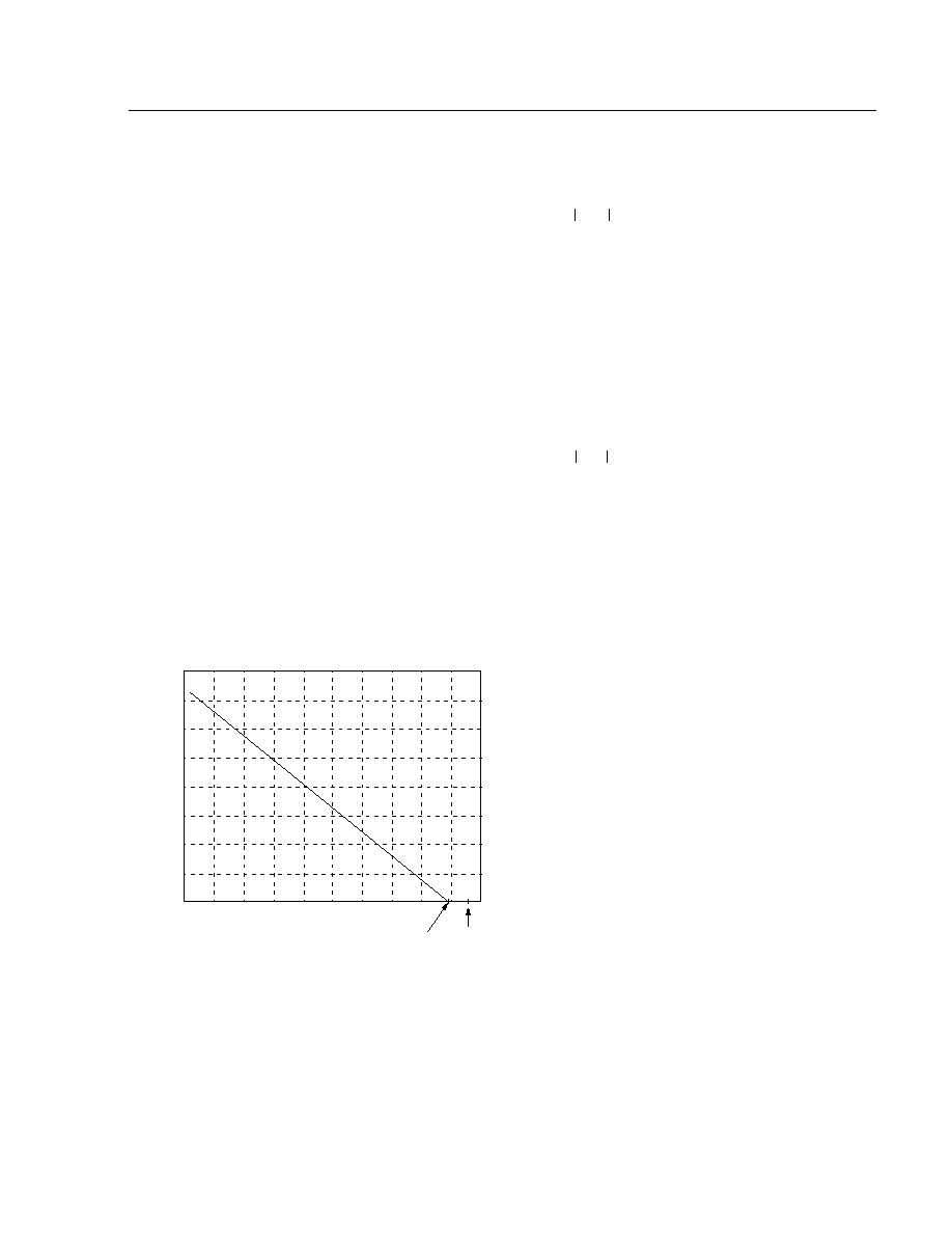
5-3428(F)
Note:
Pin numbers are
MMC A31A8575AA pin numbers. Resistors are labeled per MMC A31A8575AA description. Nodes are L8575
SLIC package nodes.
Figure 4. L8575 SLIC Resistor Module
Table 10.
MMC A31A8575AA Thick Film Resistor Module
Note: For 50 dB longitudinal balance, 0.2% for 58 dB balances. Continuous power (rms).
Resistor
Value
Tolerance
Power
Surge Rating
R
1
300
1.0%
2.0 W
Lightning: Power Cross
R
2
300
1.0%
2.0 W
Lightning: Power Cross
R
3
100 k
1.0%
250 mW
None
R
4
100 k
1.0%
250 mW
None
R
5
200 k
1.0%
250 mW
Lightning: Power Cross
R
6
200 k
1.0%
250 mW
Lightning: Power Cross
R
7
1.4 k
2.0%
0.5 W
Lightning: Power Cross
R
8
1.4 k
2.0%
0.5 W
Lightning: Power Cross
R
9
15 k
--
10 mW
None
R
9
/R
1
50
1.0%
--
--
R
1
/R
2
1
0.35%
--
--
(R
3
+ R
6
)/(R
4
+ R
5
)
1
0.35% --
--
TIP
15
FUSE
TIP
19
17
R
7
6
PR
RING
R
1
V
BAT
R
9
RGBN
GND
R
3
RS
10
9
8
7
5
FUSE
RING
1
3
R
4
TS
XMT
12
11
R
5
R
2
R
8
R
6
GND
13
PT
14
Resistors R
1
and R
2
also provide a common-mode
impedance of (300 || 300) 150
. These resistors will
primarily determine the longitudinal balance of the line
circuit; thus they must be matched appropriately to
meet longitudinal balance requirements (0.35% for
50 dB and 0.2% for 58 dB). Also, they have a signifi-
cant impact on the termination impedance of the SLIC.
Feedback using external components (external compo-
nents when a first- or second-generation codec is
used) allows the user to set the termination impedance
at 600
,
or most ITU-T recommended complex termi-
nation impedances.
Resistors R
1
and R
2
, along with R
3
and R
7
, are used in
conjunction with the self-test feature of the L8575
SLIC. In this mode, the Ring current drive amplifier is
saturated to ground, and the Tip amplifier is saturated
to battery, which causes both the ring-trip and loop clo-
sure detectors to trip. Ring-trip and loop closure detec-
tor output are bits RT and LC, respectively, in the serial
output stream.
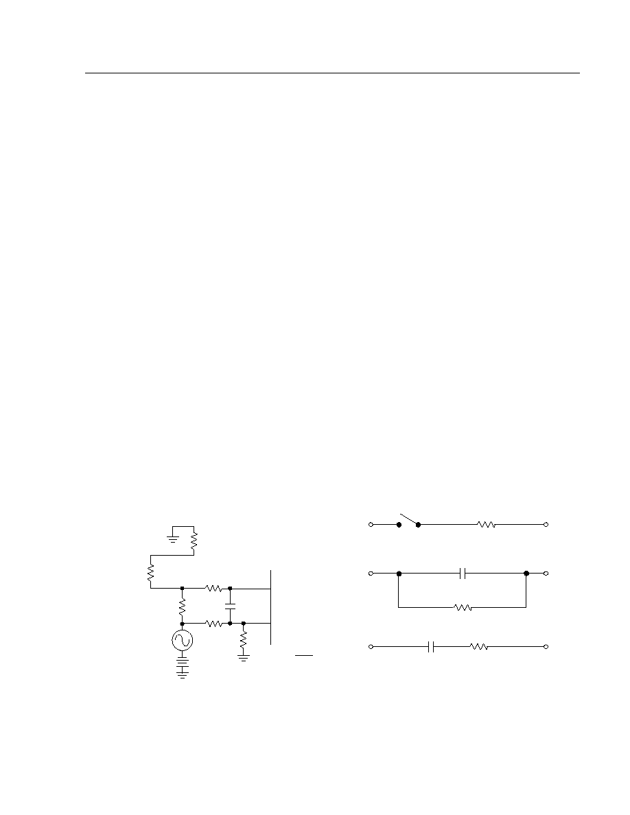
Under normal operating conditions, resistors R
1
and R
2
will see the battery voltage less the Tip/Ring voltage.
Assuming a Tip/Ring voltage of 6 V (representative of a
short into a handset), the nominal continuous operating
power of R
1
and R
2
is given by:
(48 V ≠ 6 V)
2
/600
= 2.94 W
per R
1
and R
2
resistor pair
2.94 W/2 = 1.47 W per resistor
The operating power rating of R
1
and R
2
is 2 W. This is
the steady-state power rating of R
1
and R
2
, and it is
adequate for normal operating conditions. The ability of
these resistors to withstand fault conditions depends
on the power ratings of the individual resistors and on
the power rating of the thick film resistor module itself.
Obviously, the higher the power capabilities of the
resistor module, the less susceptible the resistors are
to damage during faults. The various fault conditions
are discussed further in the Protection section of this
data sheet.

L8575
Advance Data Sheet
Dual-Resistive, Low-Cost SLIC
March 1997
18
Lucent Technologies Inc.
Applications
(continued)
Resistor Module
(continued)
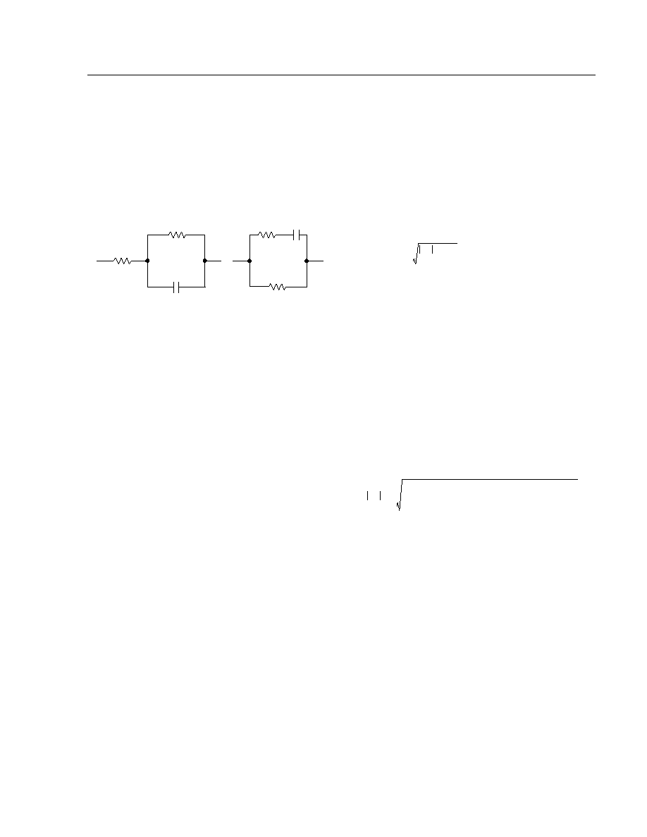
Resistors R
3
through R
6
set the gain of the SLIC in the
transmit (2-wire to 4-wire) direction. This is shown in
Figure 5.
5-3422(F)
Figure 5. L8575 SLIC Dual-Resistive Matching
Requirements
The matching of resistors R
3
through R
6
will determine
the gain accuracy of the SLIC; therefore, these resis-
tors must also be matched accordingly. The matching
requirements are given in Table 10.
Because of the high resistance values, the normal
operating power of resistors R
3
through R
6
will be rela-
tively low. Given design margin and thick film technol-
ogy capabilities, a power rating of 250 mW for these
resistors is not unreasonable.
Resistors R
7
and R
8
are used to couple the PT and PR
current drive amplifiers to Tip and Ring. Since the PT
and PR drive amplifiers are current sources, the value
of the series resistance does not affect the loop length
or other performance of the SLIC, and may be arbi-
trarily high for protection purposes. A value of 1.4 k
is
adequate for protection purposes.
Under normal operating conditions, these resistors will
see the battery voltage less the Tip/Ring voltage.
Assuming a Tip/Ring voltage of 6 V (representative of a
short into a handset), the nominal continuous operating
power of R
7
and R
8
is given by:
(48 V ≠ 6 V)
2
/2.8 k
= 0.630 W
per R
7
and R
8
resistor pair
630 mW/2 = 315 mW
per resistor (R
7
and R
8
)
Hence, the operating power rating of 500 mW for R
7
and R
8
. This is the nominal rating for R
7
and R
8
under
normal operating conditions. Again, the ability of these
resistors to withstand fault conditions depends on the
power rating.
Resistor R
9
is also included on the thick film resistor
module. This resistor is used to set the gain of the bat-
tery noise cancellation circuit. See the Battery Noise
Cancellation section of this data sheet for design equa-
tions to set the value of R
9
.
Protection
Because of the resistive feed architecture, a simple
inexpensive protection scheme that does not require a
separate external protection device may be used. The
MMC A31A8575AA resistor module has specifications
which are qualified to Bellcore GR-CORE-1089,
UL*1459, UL 497A, FCC part 68.302 (d) & (e) and REA
form 397G, ITU-T K20, and ITU-T K21.
Lightning and power cross protection are provided by
the two dc feed resistors, R
1
and R
2
, in the external
resistor module. Under fault conditions, these resistors
serve as fault current-limiting resistors. Fault current is
steered to ground and to battery via resistors R
2
and
R
1
, respectively. Thus, the battery design must be such
that the various specified faults can be applied to the
battery through 300
,
without damaging the battery or
the line circuit.
Resistors R
1
and R
2
need to be designed to survive
lightning surges and to dissipate power associated with
a Ring ground dc fault and specified ac power cross
faults--both a sneak under and full surge type fault.
Under certain sustained fault conditions, R
1
and R
2
could fail when they are required to survive. For this
reason, a per-channel fault detector is included on the
L8575 SLIC.
When the voltage across either R
1
and/or R
2
is greater
than a nominal 36 V, the fault detect bit (FLT) in the
serial data output will go high. The control logic on the
line card detects FLT is high, and opens an external
electromechanical relay (EMR) to isolate the resistors
from the loop, enabling the resistors to service
extended power cross. (Note the EMR is the test in or
test out EMR, and this relay is driven by one of the
internal relay drivers on the L8575 SLIC.)
A delay of 10 ms to 30 ms is provided (using an exter-
nal capacitor on pin CFLT) in the fault detector. This
prevents transients on the Tip and Ring from tripping
the fault detector when a fault is not present.
*
UL is a registered trademark of Underwriters Laboratories, Inc.
≠
+
TIP
RING
R
5
200 k
R
6
200 k
R
3
100 k
XMT
R
4
100 k

Advance Data Sheet
L8575
March 1997
Dual-Resistive, Low-Cost SLIC
Lucent Technologies Inc.
19
Applications
(continued)
Protection
(continued)
The Tip/Ring drive amplifiers, which feed the ac signal
to nodes PR and PT, are high-impedance current driv-
ers. Since these nodes are current sources, the value
of protection current-limiting series resistance does not
affect the loop length or other SLIC performance, and
may be arbitrarily high for protection purposes.
Resistors R
7
and R
8
in the resistor module are used for
this purpose. These resistors have a value of 1.4 k
with a power rating 0.5 W. Internal diodes clamp nodes
PR and PT to ground and battery.
The voltage sense leads, RS and TS, are also exposed
to the outside plant. Current to these nodes is limited
by resistors R
3
and R
4
in the resistor module. Resistors
R
3
and R
4
are 100 k
, 250 mW resistors. Internal
diodes also clamp nodes RS and TS to ground and
battery.
The ability of the resistors to survive faults is a function
of the power dissipated in the individual resistors and
the total power dissipated on the entire thick film mod-
ule. Fault conditions include:
s
A continuous worst-case (fault detector) sneak under
condition of 39 Vdc applied metallically to Ring in the
case of a Ring ground fault, and
s
A sneak under condition of 39 Vp (voltage peak)
applied to Tip and Ring, as described in Bellcore
1089, ITU-T K20, etc., in the case of power cross.
Additionally, there is a transient fault condition, assum-
ing full specified power cross fault voltages (Bellcore
1089, ITU-T K20, etc.,) for a time duration equal to the
maximum response time that it will take to isolate the
line circuit from the fault via the fault detector and EMR
described above.
For example, a Ring ground fault assuming fault detec-
tor sneak under will result in a worst-case potential
across the R
1
of 39 V. The power dissipated in R
1
under
this condition is calculated as follows:
(39 V * 39 V)/300
= 5 W
Since this is a sneak under condition, the fault detector
will not trigger and the time duration of the fault can be
infinite. In the case of a longitudinally applied sneak
under power cross, the maximum voltage seen, this
time by both R
1
(Ring) and R
2
(Tip), is 39 Vp (voltage
peak). The power dissipation is given by:
Maximum Voltage = 39 Vp = 27.6 Vrms
Maximum Power = (27.6 Vrms * 27.6 Vrms)/(300
)
= 2.54 W per resistor.
Thus, 2.54 W will be dissipated per resistor or a total of
5.1 W in a longitudinal sneak under condition.
If R
1
and R
2
are rated for 2 W, they can fail under these
fault conditions. Also, the
MMC A31A8575AA resistor
module includes a fail-safe thermal fuse located at the
Tip and Ring nodes (pin 1 and pin 19) of the module for
this reason. A fail-safe fuse is recommended for any
resistor module used with the L8575 SLIC.
With thick film technology, not only is the power capa-
bilities of the individual resistors important, but also the
power handling capabilities of the entire module. The
total module power dissipation is calculated by sum-
ming the power dissipation for each of the resistors
under a given condition.
For example, the module power dissipation for the
above sneak under fault conditions is calculated in
Table 11. Thus, the HIC will require a minimum power
rating of 6 W continuous to survive these sneak under
conditions.
Table 11. Total Module Power Dissipation
Resistor
(R)
Value
(
)
Ring Ground
Maximum dc
Fault Voltage (V)
Ring Ground
Maximum dc
Fault Power (W)
Longitudinal
Fault Maximum
Peak Voltage (Vp)
Longitudinal Fault
Maximum rms
Voltage (Vrms)
Longitudinal
Fault Maximum
rms Power (W)
1
300
39
5.07
39
27.577
2.535
2
300
0
0
39
27.577
2.535
3
100 k
29
0.015
39
27.577
0.0076
4
100 k
0
0
39
27.577
0.0076
5
200 k
39
0.0076
39
27.577
0.0038
6
200 k
0
0
39
27.577
0.0038
7
1.4 k
39
1.086
39
27.577
0.543
8
1.4 k
0
0
39
27.577
0.543
Total HIC Power:
6.18
--
--
6.18

L8575
Advance Data Sheet
Dual-Resistive, Low-Cost SLIC
March 1997
20
Lucent Technologies Inc.
Applications
(continued)
Protection
(continued)
Similar consideration to the individual resistor and total
module power capability should be given to full voltage
power faults, but taking into account the fault detector
will isolate the SLIC and resistor module after some
finite period of time. The fault detector indicates a fault
in the serial data output stream in 10 ns to 30 ms. Rec-
ognition and relay activation time need to be consid-
ered.
Tip/Ring Drivers
Each channel of the L8575 utilizes a current source for
the Tip/Ring driver. The driver is capable of sinking (but
not sourcing) up to 15 mA from the Tip (PT) while
swinging to within 4 V of office battery (V
BAT
), and
sourcing (but not sinking) up to 15 mA to the Ring (PR)
while swinging to within 4 V of ground (AGND). Since
the current driver is not bidirectional, during transmis-
sion (powerup) each lead is biased at 5.6 mAdc.
Receive Interface
The receive interface circuitry couples the differential
signal on receive inputs IRP and VRN to the Tip/Ring
drivers. Input IRP is a low-impedance (<5
) current
input while VRN is a high-impedance voltage input.
Internal feedback forces the voltage at IRP to be equal
to VRN such that a voltage applied to VRN causes a
current flow out of IRP, which equals that voltage
divided by the impedance connected from IRP to
AGND (assuming the input voltage is referenced to
AGND).
The receive interface and Tip/Ring drivers provide a
current gain of 200, i.e., a differential output current
flows from PT to PR which is 200 times the current
flowing into IRP. The receive interface also provides a
level shift since the inputs, IRP and VRN, are refer-
enced to analog ground, while the outputs, PT and PR,
swing between AGND and V
BAT
. The receive interface
ensures that the input current is not converted to a
common-mode current at PT and PR.
Transmit Interface
The transmit interface circuitry interfaces the differen-
tial voltage on Tip and Ring to transmit output XMT. The
Tip/Ring differential voltage (both ac and dc) appears
on output XMT with a gain of 0.5.
The transmit interface uses an operational amplifier
with four external resistors to perform a differential to
single-ended conversion. Output XMT is referenced to
ground (AGND). The longitudinal balance and gain
accuracy at XMT depends on the matching of the
external resistors.
Because a large dc potential exists at XMT, a capacitor
must be used to couple the ac signal to the low-voltage
codec circuitry. The operational amplifier inputs are TS
and RS. These inputs are also used by the fault-detec-
tion circuitry to detect fault voltages on Tip or Ring. A
fault is detected when the magnitude of the voltage
across either dc feed resistor exceeds a nominal 36 V
(equivalent to approximately 4 W dissipation in either
resistor). A delay is provided (using an external capaci-
tor on pin CFLT) in the fault detector. This prevents
transients on Tip and Ring from tripping the fault detec-
tor when a fault is not actually present.
Battery Noise Cancellation
The battery noise cancellation circuit senses the ac
noise on the battery via the capacitor connected
from input CBN to V
BAT
. It then couples this noise,
180 degrees out of phase, to the Ring current driver
amplifier. This cancels the battery noise that is coupled
to the Ring through the feed resistor connected to V
BAT
.
Additionally, it ensures longitudinal balance which
depends only on the matching of the battery feed resis-
tors by creating an ac ground at V
BAT
with respect to
signals on the Ring lead.
For the cancellation to operate properly, both the phase
and gain must be accurate. The battery noise cancella-
tion gain is a transconductance that is equal to 50
divided by resistor R9 on the thick film resistor module
connected from RGBN to ground (AGND). This value
must be equal to the reciprocal of the dc feed resistor
(1/300
), that is,
It is advantageous if the two resistors are matched and
tracked thermally, i.e., located on the same film inte-
grated circuit (FIC).
50
R
9
-------
1
300
----------------
=
R
9
15 k
=

Advance Data Sheet
L8575
March 1997
Dual-Resistive, Low-Cost SLIC
Lucent Technologies Inc.
21
Applications
(continued)
On-Hook Transmission
In powerup mode, the L8575 SLIC provides a dc bias
of 5.6 mA. The 5.6 mA bias is also present under on-
hook conditions. The L8575 SLIC is able to support on-
hook transmission because of this bias. It is sufficiently
high to drive a 3.17 dBm signal into a 600
or 900
loop under open-circuit conditions. An internal current
source provides a dc bias of 112
µ
A. There is an inter-
nal current gain of 50; thus (50 * 112
µ
A) 5.6 mA flows
from battery through R
1
to PR, and 5.6 mA flows from
PT through R
2
to ground under on-hook conditions.
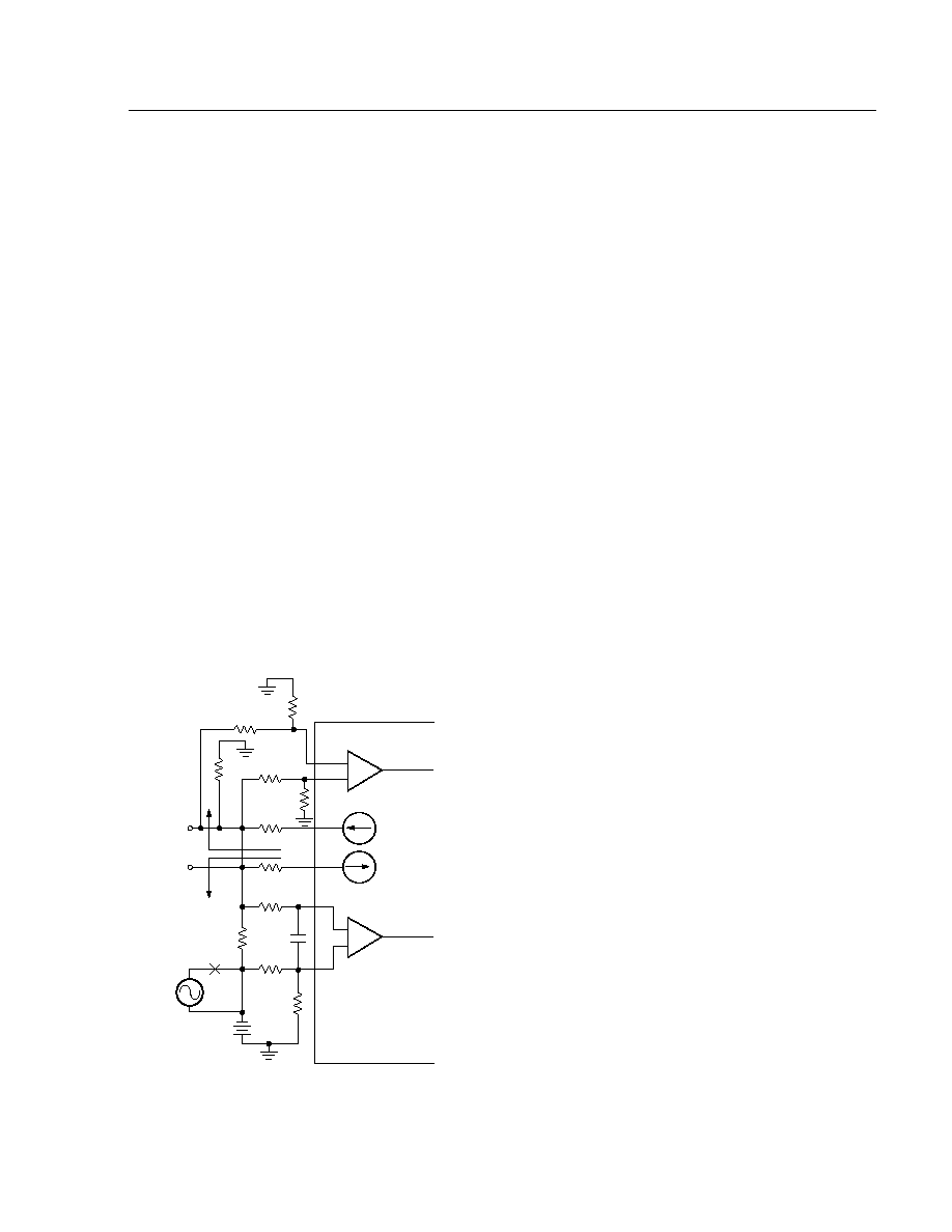
Self-Test
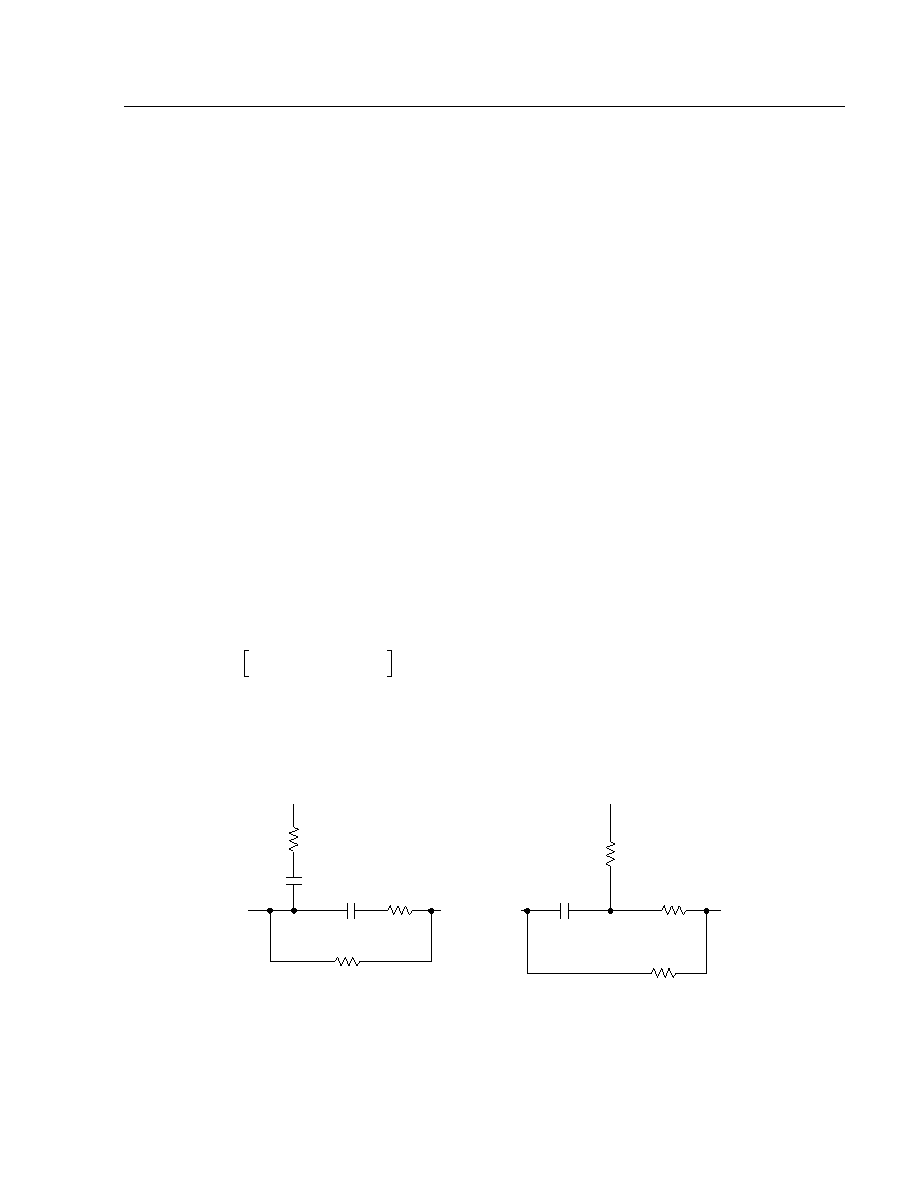
The L8575 SLIC offers a self-test capability. This is set
via logic inputs D1 and D0 in the serial input data
stream. In this mode, shown in Figure 6, the Ring cur-
rent drive amplifier is saturated to ground, and the Tip
amplifier is saturated to battery, which causes both the
ring-trip and loop closure detectors to indicate an off-
hook condition. In this operation mode, the ring relay
must not be active. The ring relay driver output in the
L8575 is at package nodes RDR (A&B). These relay
drivers are controlled by logic inputs D2 (A&B) in the
serial input data stream. See Table 14 for details.
12-3423(F).r2
Figure 6. Self-Test Mode Circuit
Serial Data Interface
A 4-wire serial interface (DI, DO, CLK, and EN) is used
to pass data from the control logic on the line card to
the L8575 SLIC, and to pass detector information from
L8575 SLIC to the control logic on the line card. When
enable input EN is high, data on input DI is clocked into
an 8-bit shift register on a high-to-low transition of the
clock input CLK.
Eight latches (four per channel) are provided to store
the data. Data is loaded into the eight latches from
input DI and the first 7 bits of the shift register on the
high-to-low transition of EN. When EN is low, a high-to-
low transition on CLK loads all of the detector informa-
tion (loop closure, fault zero voltage, and ring-trip from
the internal detector circuitry) into the 8-bit shift regis-
ter. When EN is high, data in the 8-bit shift register is
clocked out on output DO on the high-to-low transition
of CLK.
Two latch outputs per channel drive relay drivers. The
drivers are included on the L8575 SLIC. These are the
relay drivers whose outputs are at external package
nodes RDR (A&B) and RDT (A&B). The remaining two
latch output power channels are internal control sig-
nals. These are logic data bits D0 (A&B) and D1 (A&B).
These bits input to a combinational logic circuit that
controls the operational state of each channel and also
controls the state of the third relay driver. The third
relay driver's output is at external package node RDD
(A&B). Refer to the Truth Table (see Table 15) for more
details.
Note that up to 16 channels may be daisy-chained
together. The DO lead of package 1 (channels 1 and 2)
may be tied to the DI lead of package 2 (channels 3
and 4), etc. All EN and CLK should also be tied
together in this mode.
The L8575 SLIC device has an internal reset which
guarantees that all relay drivers power up in the off-
state when 5 V (V
CCD
and V
CCA
) is applied to the
device. This reset operates properly only if input EN
is held high (within 0.5 V of V
CCD
)
when the 5 V is
applied.
An external pull-up resistor from the EN bus to
V
CCD
satisfies this requirement, provided that the logic-
driving EN does not pull the EN bus low during pow-
erup.
+
≠
LCA/B
+
≠
RTA/B
PR
PTP
RTN
200 k
200 k
1.4 k
R
1.0 M
0.1
µ
F
1.0 M
8.25 M
300
V
RING
V
BAT
100 k
PT
T
1.4 k
100 k
300 k

L8575
Advance Data Sheet
Dual-Resistive, Low-Cost SLIC
March 1997
22
Lucent Technologies Inc.
Applications
(continued)
Serial Data Interface
(continued)
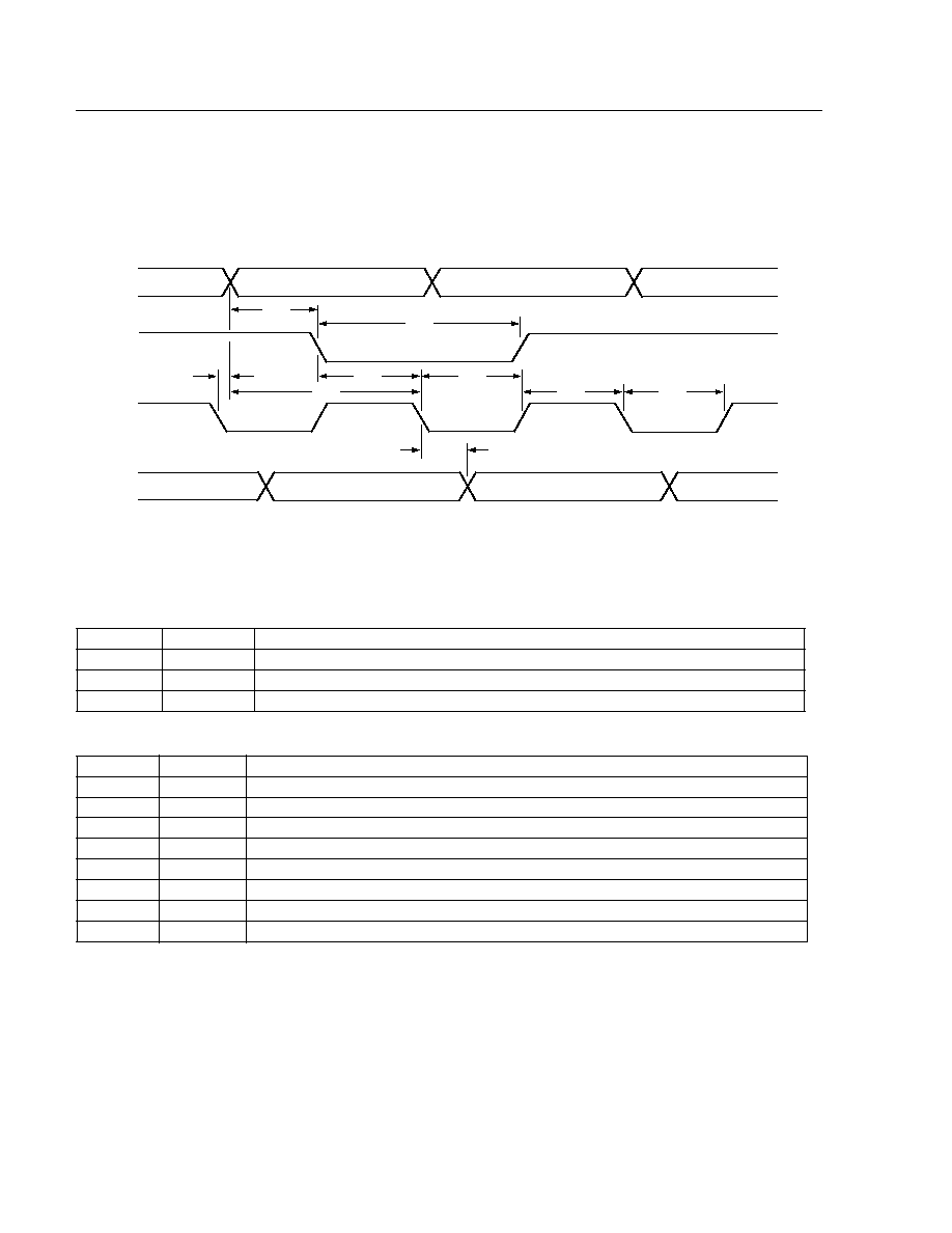
Figure 7 shows the timing characteristics and requirement definitions.
12-3305(F).ar2
Figure 7. Timing Requirements for CLK, EN, DI, and DO
Table 12. Truth Table for EN and CLK
Table 13. Output DATA Bit Definition
EN
CLK
Function
1
Shift register clocked, QN = QN ≠ 1; latches unaffected.
0
Channel data latched into shift register; latches unaffected.
X
Contents of shift register transferred to output latches.
DATA Bit
Output
Output Bit Definition
D0A
D0A
Latch output state D0A (refer to Operating States section).
D1A
D1A
Latch output state D1A (refer to Operating States section).
D2A
RDRA
Ringing relay driver A is on (RDRA low = relay energized) when D2A = 1.
D3A
RDTA
Test relay driver A is on (RDTA low = relay energized) when D3A = 1.
D0B
D0B
Latch output state D0B (refer to Operating States section).
D1B
D1B
Latch output state D1B (refer to Operating States section).
D2B
RDRB
Ringing relay driver B is on (RDRB low = relay energized) when D2B = 1.
D3B
RDTB
Test relay driver B is on (RDTB low = relay energized) when D3B = 1.
DI
EN
CLK
DO
t
SDE
t
WEN
t
HDC
t
SDC
t
HEC
t
SEC
t
WCK
t
WCK
t
PCO

Advance Data Sheet
L8575
March 1997
Dual-Resistive, Low-Cost SLIC
Lucent Technologies Inc.
23
Electrical Characteristics
(continued)
Serial Data Interface
(continued)
Table 14. Input DATA Bit Definition
12-3306(F).br3
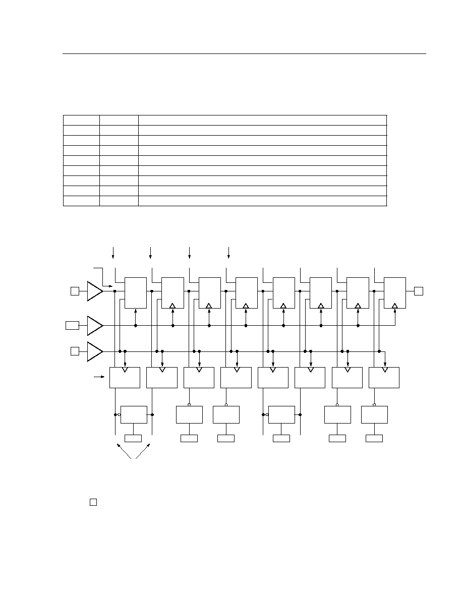
Figure 8. Logic Diagram (Positive Logic; Flip-Flops Clocked on High-to-Low Transition)
Input
DATA Bit
Input Bit Definition
RZA
D0A
Channel A ringing voltage zero crossing detector output (positive = 1).
FLTA
D1A
Channel A fault detector output (loop fault = 1).
RTA
D2A
Channel A ring-trip detector output (ring-trip = 1).
LCA
D3A
Channel A switchhook detector output (off-hook = 1).
RZB
D0B
Channel B ringing voltage zero crossing detector output (positive = 1).
FLTB
D1B
Channel B fault detector output (loop fault = 1).
RTB
D2B
Channel B ring-trip detector output (ring-trip = 1).
LCB
D3B
Channel B switchhook detector output (off-hook = 1).
RZA
D0
D1
SEL
Q
D
Q
Q
D0A
D0A
DI
CLK
EN
FLTA
D0
D1
SEL
Q
D
Q
Q
D1A
D1A
RTA
D0
D1
SEL
Q
D
Q
Q
D2A
RDRA
LCA
D0
D1
SEL
Q
D
Q
Q
D3A
RDTA
RZB
D0
D1
SEL
Q
D
Q
Q
D0B
D0B
FLTB
D0
D1
SEL
Q
D
Q
Q
D1B
D1B
RTB
D0
D1
SEL
Q
D
Q
Q
D2B
RDRB
LCB
D0
D1
SEL
Q
D
Q
Q
D3B
RDTB
DO
RELAY
DRIVER
RELAY
DRIVER
RELAY
DRIVER
RELAY
DRIVER
RELAY
DRIVER
RDDB
RELAY
DRIVER
RDDA
FROM
RING VOLTAGE
ZERO DETECT
CIRCUIT
FROM
FAULT DETECT
CIRCUIT
INTERNAL
INTERNAL
FROM
RING-TRIP
CIRCUIT
INTERNAL
FROM
LOOP CLOSURE
CIRCUIT
INTERNAL
8-bit SHIFT
RESISTOR
DATA
LATCHES
TO INTERNAL STATE CONTROL
COMBINATIONAL LOGIC CIRCUITRY
INDICATES EXTERNAL PACKAGE MODE

L8575
Advance Data Sheet
Dual-Resistive, Low-Cost SLIC
March 1997
24
Lucent Technologies Inc.
Operating States
Each channel of the L8575 has four operating states:
active, test, powerdown with relay driver RDD ON, and
powerdown with relay driver RDD OFF. These states
are selected using 2 bits, D0 and D1, via the serial
interface according to the truth table shown below.
Table 15. Truth Table for D1 and D0
Logic input D2 operates the ringing relay driver, RDR,
independent of the state of bits D0 and D1; however,
the ring-trip detector is enabled only when D2 operates
the ringing relay driver. Hence, the ringing relay driver
is not interchangeable with any of the other relay driv-
ers. Logic input D3 operates the test relay driver, RDT,
independent of the state of bits D0 and D2.
Active State
This is the normal operating state (talk state) of the
channel. All circuits are operational. The Tip drive cur-
rent source sinks 5.6 mAdc from PT; the Ring drive
current source sinks 5.6 mAdc into PR.
Test State
This is the test state of the channel. It is the same as
the active state except that the Ring drive current
source is saturated to ground and the Tip driver current
source is saturated to V
BAT
. This forces the loop-closure
and ring-trip detectors to indicate an off-hook. This
state is valid only when the ringing relay is not operated
(D2 = 0).
Powerdown State with Relay Driver RDD
Operated
This is the disconnect state of the channel. It is the
same as the powerdown state except that relay driver
RDD is also operated. When required, this relay may
be used to disconnect the external dc feed resistors in
order to provide a high-impedance termination to the
subscriber loop.
Powerdown State
This is the normal idle state (scan state) of the channel.
The loop-closure, ring-trip, and common-mode fault
detectors are active, but all other circuits are shut down
to conserve power. All circuits common to both chan-
nels remain active. The powerdown of channel A does
not affect an active channel B and vice-versa.
Ringing State (D2 = 1)
When D2 = 1, the ringing relay driver is activated. The
operational state of the SLIC is unaffected except for
the ring-trip and fault detectors. The digital portion of the
ring-trip detector is enabled when D2 = 1 (relay drive ac-
tivated) and disabled when D2 = 0 (relay drive deacti-
vated). The ring-trip detector functions properly only
when D2 = 1 so that a valid ringing signal (ac and dc) is
present. When D2 = 0, the digital portion of the ring-trip
detector is bypassed so that most of the ring-trip circuit
can be tested in the test state. When D2 = 1, the fault
detector is also disabled (FLT forced to 0).
D1
D0
State
1
1
Channel Active.
1
0
Channel Test.
0
1
Channel Powerdown and
Relay RDD driver ON (RDD low).
0
0
Channel Powerdown. Relay RDD
driver OFF/RDD high.

Lucent Technologies Inc.
25
Advance Data Sheet
L8575
March 1997
Dual-Resistive, Low-Cost SLIC
Supervision
Off-Hook Detection
The off-hook detection threshold is a function of the dc
feed resistors R
1
and R
2
, and of a ratio of resistors that
are fixed on the L8575 silicon die.
Thus, when R
1
= R
2
= 300
, the off-hook threshold is
set at 4 k
. This relationship is shown in the equation
below:
Where,
R
T
is the loop closure threshold
R
1
= R
2
= dc feed resistors = 300
Where,
R
T1
and R
T2
are internal resistors
R
T1
= 170 k
R
T2
= 130 k
Thus,
Ring-Trip Threshold
12-3424(F)
Figure 9. Ring-Trip Threshold
Ring-trip threshold (Figure 9) is calculated as follows:
At ring-trip:
If,
V
BAT
= V
20 Hz (dc)
Then,
R
RTH
= R
RF
R
RF
= 1 M
; R
L
(ring-trip) = 6 k
[Avg: 2 k
& 10 k
]
Ring-Trip Requirements
s
Ringing signal:
-- Voltage: minimum 35 Vrms, maximum 100 Vrms.
-- Frequency: 17 Hz to 23 Hz.
-- Crest factor: 1.4 to 2.
s
Ringing trip:
--
100 ms (typical),
250 ms (V
BAT
= ≠33 V,
loop length = 530
).
s
Pretrip:
-- The circuits in Figure 10 will not cause ringing trip.
12-2572 (C)
Figure 10. Ring-Trip Circuits
R
T
R
1
R
2
+
1
2 k
------------
1
≠
----------------------
=
K
R
T1
R
T1
R
T2
+
---------------------------
0.4333
=
=
R
T
300
300
+
1
2
130 k
130 k
170 k
+
---------------------------------------------
------------------------------------------------------
1
≠
----------------------------------------------------------------
3900
4
k
=
=
LOOP
RESISTANCE
R
L
TIP
RING
300
R
RF
R1
300
R
RF
R
RTH
C
RF
RTN
RTP
V
RTN
(dc) =
V
BAT
Z
V
BAT
2
--------------
R
RF
R
RTH
---------------
300
R
L
600
+
-------------------------------
V
20 Hz (dc)
=
R
RF
2R
RTH
------------------
300
R
L
600
+
------------------------------
=
1
R
L
600
-------------------
+
R
RTH
= 11 M
2R
RF
C
RF
100 ms
C
RF
= 0.047
µ
F
RING
RING
RING
100
10 k
6 µF
TIP
TIP
TIP
2 µF
200
SWITCH CLOSES < 12 ms

L8575
Advance Data Sheet
Dual-Resistive, Low-Cost SLIC
March 1997
26
Lucent Technologies Inc.
Supervision
(continued)
Fault Detection
The dc feed resistors R
1
and R
2
need to be designed to
survive lightning surges and to dissipate power associ-
ated with a Ring ground dc fault and specified ac power
cross faults--both in a sneak under and full surge type
fault.
Under certain sustained fault conditions, R
1
and R
2
could fail when they are required to survive. For this
reason, a per-channel fault detector is included on the
L8575. When the voltage across either R
1
and R
2
is a
nominal 36 V (maximum 39 V), the fault detect bit, FLT
in the serial data output, will go high, as calculated
below:
FLT = 1, if
|V
TIP
| > 36 V nominal
or
|V
RING
≠ V
BAT
| > 36 V nominal, which corresponds
to dc power in R
1
or R
2
> 4 W
The control logic on the line card detects FLT is high
and opens an external electromechanical relay to iso-
late the resistors from the loop, enabling the resistors
to survive extended power cross. (Note the EMR is the
test in or test out EMR, and this relay is driven by one
of the internal relay drivers on the L8575 SLIC.)
With an external 0.1
µ
F capacitor on pin CFLT, a no-
fault to fault delay of 10 ns to 30 ms is provided in the
fault detector. This prevents transients on Tip and Ring
from tripping the fault detector when a fault is not
present. There is a release delay (fault to no-fault) of
1.6 T to 2.5 T, where T is the no-fault to fault delay time.
Zero Voltage Current Cross
The L8575 provides a bit, RZA (and RZB for channel B),
in the serial data stream which gives an indication when
the ringing voltage is crossing zero. This signal bit may
be used in timing the application and removal of the
ringing signal.
Relay Drivers
Six relay drivers, three relay drivers per channel, are
included on the L8575 SLIC. The output of these driv-
ers are package nodes RDD (A&B), RDR (A&B), and
RDT (A&B). Drivers RDR (A&B) are controlled by input
bits D2 (A&B) on the serial input stream. Drivers
RDT(A&B) are controlled by input bits D3 (A&B) on the
serial input stream. In these cases, a logic 1 on D2 or
D3 activates the respective relay driver.
Relay drivers RDD (A&B) are controlled per the truth
table (see Table 2) via bits D0 (A&B) and D1 (A&B). In
order to activate driver DDR, D0 = logic 1 and
D1 = logic 0. Note that with D0 = logic 1 and
D1 = logic 0, the SLIC is set to the channel powerdown
state.
Relay drivers RDR (A&B) must be used for the Ring
relay function because the ring-trip detector is enabled
only when D2 is high; that is, when D2 operates the
ringing relay driver (RDR). Hence, the test and ringing
relay drivers are not interchangeable.
When relay driver RDD is active, the L8575 is forced
into a powerdown state. Thus, using RDD with the test-
in relay is not appropriate. This relay may be used for
test out or as a channel isolation relay.
Relay driver RDT is controlled by D3 in the serial bit
stream. Logic input D3 operates driver RDT indepen-
dent of the state of bits D0, D1, and D2. RDT may be
used with a test-in, test-out, or channel isolation relay.

Advance Data Sheet
L8575
March 1997
Dual-Resistive, Low-Cost SLIC
Lucent Technologies Inc.
27
dc Characteristics
I/V Characteristics
Resistors R
1
and R
2
are the dc feed resistors. R1 is
connected from battery to Ring, and R2 is connected
from Tip to ground. The dc loop current is fed to the
subscriber loop via these resistors. These resistors will
set the dc I/V template for the line circuit, with the I/V
template being linear with a ≠1/600
slope. No con-
stant current region at short dc loops is provided by
resistors R
1
and R
2
or the L8575 SLIC.
The dc Tip/Ring voltage under open loop conditions is
3.36 V less than battery. In order to drive an on-hook ac
signal, the Tip and Ring voltage must be set to a value
less than the battery voltage. The amount that the open
loop voltage (V
OC
) is decreased relative to the battery
(V
BAT
) is referred to as the overhead voltage (V
OH
). This
overhead voltage is due to 5.6 mA of bias current flow
from both the Tip and Ring current drive amplifier's flow
through resistors R2 and R1, respectively. Thus, the
overhead is given by:
V
OH
= (R
1
x 5.6 mA) + (R
2
x 5.6 mA)
V
OH
= (300 x 5.6 mA) + (300 x 5.6 mA) = 3.36 V
The nominal dc I/V template for the L8575 SLIC is
shown in Figure 11.
12-3430(F).r1
Figure 11. L8575 SLIC I/V Template
Loop Length
The loop range equation is given by:
Where,
R
L
is the dc resistance of the subscriber loop.
I
L
is the dc loop current.
|V
BAT
| is the magnitude of the battery voltage.
V
OH
is the overhead voltage--nominal 3.36 V.
R
1
= R
2
= dc feed resistors = 300
.
Thus, for a nominal ≠48 V battery with a minimum
18 mA loop requirement, the loop range will be:
R
L
= 1880
20
80
60
0
5
10
15
20
35
40
0
70
50
30
10
25
30
40
45
50
V
T-R
(V)
I
LOOP
(mA)
V
OC
(44.7)
V
BAT
(48)
R
L
V
BAT
V
OH
≠
I
L
----------------------------------
R
1
≠
R
2
≠
=
R
L
48 V
3.36 V
≠
0.018 A
---------------------------------------
300
≠
300
≠
=

L8575
Advance Data Sheet
Dual-Resistive, Low-Cost SLIC
March 1997
28
Lucent Technologies Inc.
ac Design
Codec Features and Selection Summary
There are four key ac design parameters:
s
Termination impedance is the impedance looking
into the 2-wire port of the line card. It is set to match
the impedance of the telephone loop in order to mini-
mize echo return to the telephone set.
s
Transmit gain is measured from the 2-wire port to the
PCM highway.
s
Receive gain is done from the PCM highway to the
transmit port.
s
Hybrid balance network cancels the unwanted
amount of the receive signal that appears at the
transmit port.
At this point in the design, the codec needs to be select-
ed. The discrete network between the SLIC and the co-
dec can then be designed. Below is a brief codec
feature and selection summary.
First-Generation Codecs
These perform the basic filtering, A/D (transmit), D/A
(receive), and
µ
-law/A-law companding. They all have
an op amp in front of the A/D converter for transmit gain
setting and hybrid balance (cancellation at the summing
node). Depending on the type, some have differential
analog input stages, differential analog output stages,
and
µ
-law/A-law selectability. This generation of codec
has the lowest cost. It is most suitable for applications
with fixed gains, termination impedance, and hybrid
balance.
Second-Generation Codecs
This class of devices includes a microprocessor inter-
face for software control of the gains and hybrid bal-
ance. The hybrid balance is included in the device. ac
programmability adds application flexibility and saves
several passive components. It also adds several I/O
latches that are needed in the application. It does not
have the transmit op amp, since the transmit gain and
hybrid balance are set internally.
Third-Generation Codecs
This class of devices includes the gains, termination im-
pedance, and hybrid balance--all under microproces-
sor control. Depending on the device, it may or may not
include latches.
In the codec selection, increasing software control and
flexibility are traded for device cost. To help decide, it
may be useful to consider the following:
s
Will the application require only one value for each
gain and impedance?
s
Will the board be used in different countries with dif-
ferent requirements?
s
Will several versions of the board be built? If so, will
one version of the board be most of the production
volume?
s
Does the application need only real termination
impedance?
s
Does the hybrid balance need to be adjusted in the
field?

Advance Data Sheet
L8575
March 1997
Dual-Resistive, Low-Cost SLIC
Lucent Technologies Inc.
29
ac Design
(continued)
Design Equations
The following section gives the relevant design equa-
tions to choose component values for any desired gain,
termination and balance network, assuming a complex
termination is desired. Complex termination will be
specified in one of the two forms shown below:
12-3425(F)
Figure 12. Equivalent Complex Terminations
Both forms are equivalent to each other, and it does
not matter which form is specified. The component val-
ues in the interface circuit of Figure 12 are calculated
assuming the parallel form is specified. If the termina-
tion impedance to be synthesized is specified in the
series form, convert it to the parallel form using the
equations below:
Note that if the termination impedance is specified as
pure resistive:
Define the gain constant, K, as follows:
Where,
R
X
= desired receive (or PCM to Tip/Ring)
gain in dB
T
X
= desired transmit (or Tip/Ring to PCM)
gain in dB
|Z
T
| 1 kHz is the magnitude of the complex termina-
tion impedance Z
T
being synthesized, calculated at
1000 Hz. This equation assumes that the TLP of the
codec is 0 dBm referenced to 600
.
The following equation applies when referring to
Figure 13:
Where,
= 2
= 1000 Hz
CR
1
R
2
is defined per Figure 12 (series form), and
R1
R2
C
R2¥
R1¥
C¥
(SERIES FORM)
(PARALLEL FORM)
R
1
R
1
R
2
+
=
R
2
R
1
2
R
2
R
1
+
R
2
-------------------------------
=
C
C
1
2
R
1
R
2
-------
R
1
R
2
-------
2
+
+
-------------------------------------------
=
R
2
R
2
0 and C = C
=
=
=
K
RCV
K
0
10
Rx/20
for receive gain
=
K
TX
1
K
0
------
10
Tx/20
for transmit gain
=
K
0
Z
T
1
kHz
600
--------------------------
=
= power transfer ratio
Z
T
2
C
2
R
1
R
2
2
R
1
R
2
j
R
2
2
C
≠
+
+
1
2
R
2
2
C
2
+
---------------------------------------------------------------------------------------
=
Z
T
2
C
2
R
1
R
2
2
R
1
R
2
+
+
1
2
R
2
2
C
2
+
-----------------------------------------------------------
2
R
2
2
C
1
2
R
2
2
C
2
+
-----------------------------------
2
+
=

L8575
Advance Data Sheet
Dual-Resistive, Low-Cost SLIC
March 1997
30
Lucent Technologies Inc.
ac Design
(continued)
Design Equations
(continued)
12-3429.C (F)
Figure 13. Initial ac Interface for Complex Termination Between L8575 SLIC and T7504 Codec
Note: dc Blocking Capacitors (C
B
) Not Shown, C
T
and C
R
Separate
V
RN
RECEIVE
INTERFACE
+
≠
R
T2
R
RV2
R
HB1
R
GX
GSX
VFXIN
VFRO
1/4 T7504 CODEC
Z
T/R
+
≠
V
T/R
I
T/R
+2.4 V
C
R
1/2 L8575
R
GX1
R
RV1
C
T
R
T1
Z
IRP
≠
+
AX
V
XMT
L
RP
V
RN
XMT
I
RP
PT
PR
V
BAT
TS
RS
V
BAT
R
1
R
2
C
1
RESISTOR
MODULE
200 k
200 k
100 k
300
300
100 k
1.4 k
1.4 k

Advance Data Sheet
L8575
March 1997
Dual-Resistive, Low-Cost SLIC
Lucent Technologies Inc.
31
ac Design
(continued)
Design Equations
(continued)
The Tip/Ring differential current is given by:
The voltage at pin XMT is given by:
The component values in the ac interface of Figure 13
are calculated (for the transmit and receive gains
defined by the respective gain constants K
RX
and K
RCV
,
and for the termination impedance seen in Figure 12)
using the following equations:
600
= 2 x 300
feed resistors
R
GX
= 2 x K
TX
(R
GX1
+ R
T1
)
The 300
feed resistors contribute 600
to the termi-
nation impedance. The termination impedance associ-
ated with the circuit in Figure 13 consists of this
inherent 600
feeding impedance in parallel with:
s
A negative impedance, where,
x
s
A positive impedance, where,
x
The negative and positive impedance terms are used
to adjust the termination impedance from the inherent
600
to any complex termination.
Note in the case of a pure 600
dc termination, the
two 300
feed resistors provide this termination, and
components R
T1
, R
T2
, and C
T
are not used in the ac
interface circuit.
Using the circuit of Figure 13, the ratio of capacitors C
T
and C
R
will affect the (transmit and receive) gain flat-
ness, and to a lesser degree the return loss of the line
circuit. Thus, depending on the requirements, C
T
and
C
R
may need to be tight tolerance capacitors.
If this is the case, capacitors C
T
and C
R
may be com-
bined into a single capacitor with a looser tolerance.
This is illustrated in Figure 14.
I
T/R
200 I
RP
V
RN
Z
IRP
-----------
≠
=
V
XMT
V
T/R
≠
2
--------------
=
R
RV1
100R
1
K
RCV
-------------------
=
R
RV2
100R
2
K
RCV
-------------------
=
C
R
K
RCV
C
100
--------------------
=
R
GX1
R
GX1
R
T1
+
------------------------------
R
RV1
100
-------------
1
600
----------
1
R
1
--------
≠
=
C
T
C
100
---------- 1
R
GX1
R
T1
------------- 1
100R
1
R
RV1
-------------------
+
+
=
R
T2
R
2
C
C
T
---------------
=
2
100
----------
R
GX1
R
GX1
R
T1
+
------------------------------
R
T2
1
j
C
T
-------------
+
R
GX1
R
T1
+
R
T1
------------------------------
12-3426a(F)
Figure 14. Revised ac Interface C
T
and C
R
Combined into a Single Capacitor C
S
XMT
RT2
C
T
IRP
C
R
V
FRO
RRV2
XMT
RT2
IRP
C
S
= C
T
+ C
R
V
FRO
RRV2
RRV1
RRV1
--
--
--

L8575
Advance Data Sheet
Dual-Resistive, Low-Cost SLIC
March 1997
32
Lucent Technologies Inc.
ac Design
(continued)
Design Equations
(continued)
To scale C
S
(higher), increase C
T
(and decrease R
T2
)
by increasing the R
GX1
/ (R
GX1
+ R
T1
) ratio by rearrang-
ing the circuit in Figure 13 and by adding resistor R
SC
from XMT to IRP as shown in the figure below:
12-3427a(F)
Figure 15. Addition of Resistor R
SC
from XMT to IRP
Then,
Once the gains and complex termination are set, if the
hybrid balance network is identical to the termination
impedance, then the hybrid balance is set by a single
resistor (shown in Figure 15) and is computed as fol-
lows:
The L8575 SLIC is ground referenced. However, a +5 V
only codec, such as T7504, is referenced to +2.5 V. The
L8575 SLIC has sufficient dynamic range to accommo-
date an ac signal from the codec that is referenced to
+2.5 V without clipping distortion.
With a ≠48 V battery, the dc voltage at node XMT will
be a nominal ≠22 V or
≠ 4 V. This is the
common-mode dc voltage. This will cause a dc current
flow from the codec to the SLIC. This current will not
affect ac performance, but it will effectively waste
power. To avoid this wasted power consumption, block-
ing capacitors can be added. The blocking capacitors
block the dc path from any low impedance node at the
codec to SLIC node XMT. Blocking capacitors are
added to the application diagram in Figure 16.
After the blocking capacitor C
B
is added, the above
component values may have to be adjusted slightly to
optimize performance.
The effects of the blocking capacitor are best evaluated
and optimized by circuit simulation. Contact your
Lucent Technologies Microelectronics Group Account
Representative for information on availability of a
PSPICE* model.
Figure 16 shows a complete reference design using the
L8575 SLIC and T8502/3 codec. This line circuit is
designed to meet the requirements of the People's
Republic of China. The basic ac design parameters are
listed below:
Termination impedance: 200
+ 680
||
0.1
µ
F
Hybrid balance network: 200
+ 680
||
0.1
µ
F
Transmit gain: 0 dB
Receive gain: ≠3.5 dB or ≠7.0 dB
Notice that the interface circuit between the L8575 and
T8502/3 is designed for a receive gain of ≠3.5 dB.
The T8502 codec offers a pin selectable receive gain of
0 dB or ≠3.5 dB. Thus, via logic control, a receive gain
of either ≠3.5 dB or 7.0 dB is achieved.
The T8502/3 codec is a dual +5 V only codec. When
used with the dual L8575 SLIC, a complete low-cost,
dual-line circuit is achieved.
*
PSPICE is a registered trademark of MicroSim Corporation.
R
T1
R
SC
IRP
C
T
R
T2
XMT
VRN
R
GX1
C
B
R
GX1
R
GX1
R
T1
+
------------------------------
R
RV1
R
SC
||
(
)
100
-------------------------------------
1
600
----------
1
R
1
---------
≠
R
RV1
R
RV1
R
SC
+
------------------------------
+
=
R
HB
R
GX
K
RCV
K
◊
TX
--------------------------------
=
V
TIP
V
RING
≠
(
)
2
-----------------------------------------

Advance Data Sheet
L8575
March 1997
Dual-Resistive, Low-Cost SLIC
Lucent Technologies Inc.
33
Application Diagram
The following diagram and table show the basic components required with the L8575 SLIC. Specific component
values are given in cases where the value is fixed. In cases where the value may change (i.e., components that
determine the ac interface), the value is not listed but equations to determine these values are given later in this
document.
Table 16. External Components Required
* Power is continuous RMS power.
R
1
/R
2
= 1, with a tolerance of 0.35% for 50 dB longitudinal balance, 0.2% for 58 dB longitudinal balance. Fuses on F1 and F2 provide fail-safe
operation if excessive overvoltage conditions exist on Tip and Ring. They will not operate if the total power dissipation of the entire resistor
network is >5.0 W at 85
∞
C.
(R
3
x R
6
)/(R
4
x R
5
) = 1 with a tolerance of 0. 35% for 50 dB longitudinal balance, 0.2% for 58 dB longitudinal balance.
ß R
9
/R
1
= 100 with a tolerance of 0.5%.
Comp. Function
Implementation
Value
Attribute*
R
1
dc Feed Protection
Resistor Module
300
1.0%, 2 W
R
2
dc Feed Protection
Resistor Module
300
1.0%, 2 W
R
3
Transmit Gain
Resistor Module
100 k
1.0%, 25 mW
R
4
Transmit Gain
Resistor Module
100 k
1.0%, 25 mW
R
5
Transmit Gain
Resistor Module
200 k
1.0%, 25 mW
R
6
Transmit Gain
Resistor Module
200 k
1.0%, 25 mW
R
7
Protection
Resistor Module
1.4 k
2.0%, 0.1 W
R
8
Protection
Resistor Module
1.4 k
2.0%, 0.1 W
R
9
Battery Noise Cancellation
Resistor Module
15 k
10 mW
ß
C
VCC
V
CC
Filter
External
0.1
µ
F
20%, 10 V
C
VDD
V
DD
Filter
External
0.1
µ
F
20%, 10 V
C
BAT
V
BAT
Filter
External
0.1
µ
F
20%, 100 V
R
CBN
Battery Noise Cancellation
External
301 k
1%, 1/16 W
C
CBN
Battery Noise Cancellation
External
0.1
µ
F
20%, 100 V
C
RF
Ring Trip
External
0.1
µ
F
20%, 100 V
R
RF1
Ring Trip
External
1 M
20%, 100 V
R
RF2
Ring Trip
External
1 M
1%, 1/16 W
R
RTH
Ring Trip Threshold
External
11 M
1%, 1/16 W
C
FLTA
Fault Filter
External
0.1
µ
F
20%, 100 V
C
B1
dc Blocking
External
0.1
µ
F
20%, 50 V
C
B2
dc Blocking
External
0.1
µ
F
20%, 50 V
R
T1
ac Interface
External
34 k
1%, 1/32 W
R
T2
ac Interface
External
7.32 k
1%, 1/32 W
R
GX
ac Interface
External
150 k
1%, 1/32 W
R
GX1
ac Interface
External
52.3 k
1%, 1/32 W
R
RV1
ac Interface
External
113 k
1%, 1/32 W
R
RV2
ac Interface
External
35.7 k
1%, 1/32 W
C2 or C
S
ac Interface
External
2.7 nF
5%, 10 V
R
HB1
ac Interface
External
221 k
1%, 1/32 W

L8575
Advance Data Sheet
Dual-Resistive, Low-Cost SLIC
March 1997
34
Lucent Technologies Inc.
Application Diagram
(continued)
12-3308(F).a
Figure 16. Typical Application Diagram with Blocking Capacitors (C
B
) Included
18
PTB
13
TSB
12
XMTB
14
RSB
44
CLK
43
EN
3
DI
2
DO
1.4 k
KTA
37
38
30
7
+5 D
RDTA
RDRA
RDDA
RDDB
PTA
TSA
300
200 k
28
33
34
XMTA
100 k
XMTA
KTA2
TIP
TEST OUT
BUS
(CHANNEL A)
KTA1
RING
100 k
200 k
1.4 k
32
RSA
27
PRA
36
RTPA
KRA2
1 M
0.1
µ
F
35
RTNA
1 M
300
11 M
KRA1
VRNG
(RINGING
V
BAT
19
PRB
10
RTPB
11
RTNB
301 k
CBNA
24
CBNB
22
0.1
µ
F
0.1
µ
F
V
BAT
V
BAT
21, 25
0.1
µ
F
AGND
20, 26
V
DDA
23
+5 A
SAME AS
CHANNEL A
SAME AS
CHANNEL A
4
CFLTB
15
RGBNB
16
VRNB
17
IRPB
C
B2
R
RV2
R
T2
XMTA
TERMINATION/HYBRID
200
+ 680
II
0.1
µ
F
2.7 nF
29
IRPA
113 k
0.1
µ
F
XMTA
221 k
52.3 k
R
GX
34 k
30
VRNA
VFRO(n)
VFXIN(n)
GSX(n)
1/2 T8502/3
CODEC
15 k
31
RGBNA
0.1
µ
F
42
CFLTA
SERIAL INTERFACE
BUSES TO
CONTROL LOGIC
8
RDRB
9
RDTB
5, 41
V
DDD
0.1
µ
F
DG
6, 40
DGND
(OFFICE BATTERY)
THICK FILM
RESISTOR
R
X
= ≠3.5 dB/≠7.0 dB
R
RTH
R
F2
R
2
R
8
R
6
R
4
R
3
R
5
R
F1
THICK FILM
RESISTOR
C
RF
R
1
MODULE
SUPPLY)
MODULE
R
7
L8575
R
9
KTA
KTA
KTB
KTB
KTB
35.7 k
7.32 k
0.1
µ
F
150 k
R
T1
R
RV1
C
S
= C
T
+ C
R
R
GX1
C
B1
R
HB2
C
VDD
C
FLTA
T
X
= 0 dB
GS
GAIN
C
CBN
C
BAT
C
VCC
R
CBN
SELECT

Advance Data Sheet
L8575
March 1997
Dual-Resistive, Low-Cost SLIC
Lucent Technologies Inc.
35
Outline Diagram
44-Pin PLCC
Dimensions are in millimeters.
5-2506r7
4.57
MAX
1.27 TYP
0.53
MAX
0.10
SEATING PLANE
0.51 MIN
TYP
1
6
40
7
17
29
39
18
28
PIN #1 IDENTIFIER
ZONE
16.66 MAX
17.65 MAX
16.66
MAX
17.65
MAX

L8575 Advance Data Sheet
Dual-Resistive, Low-Cost SLIC March 1997
For additional information, contact your Microelectronics Group Account Manager or the following:
INTERNET: http://www.lucent.com/micro
U.S.A.: Microelectronics Group, Lucent Technologies Inc., 555 Union Boulevard, Room 30L-15P-BA, Allentown, PA 18103
1-800-372-2447, FAX 610-712-4106 (In CANADA: 1-800-553-2448, FAX 610-712-4106), e-mail docmaster@micro.lucent.com
ASIA PACIFIC: Microelectronics Group, Lucent Technologies Singapore Pte. Ltd., 77 Science Park Drive, #03-18 Cintech III, Singapore 118256
Tel. (65) 778 8833, FAX (65) 777 7495
JAPAN: Microelectronics Group, Lucent Technologies Japan Ltd., 7-18, Higashi-Gotanda 2-chome, Shinagawa-ku, Tokyo 141, Japan
Tel. (81) 3 5421 1600, FAX (81) 3 5421 1700
For data requests in Europe:
MICROELECTRONICS GROUP DATALINE: Tel. (44) 1189 324 299, FAX (44) 1189 328 148
For technical inquiries in Europe:
CENTRAL EUROPE: (49) 89 95086 0 (Munich), NORTHERN EUROPE: (44) 1344 865 900 (Bracknell UK),
FRANCE: (33) 1 41 45 77 00 (Paris), SOUTHERN EUROPE: (39) 2 6601 1800 (Milan) or (34) 1 807 1700 (Madrid)
Lucent Technologies Inc. reserves the right to make changes to the product(s) or information contained herein without notice. No liability is assumed as a result of their use or application. No
rights under any patent accompany the sale of any such product(s) or information.
Copyright © 1997 Lucent Technologies Inc.
All Rights Reserved
March 1997
DS97-140ALC (Replaces DS96-099LCAS)
Printed On
Recycled Paper
Ordering Information
Device Part No. Description Package Comcode
LUCL8575 BP Dual-Resistive SLIC 44-pin PLCC 107890386
LUCL8575 BP-TR Dual-Resistive SLIC 44-pin PLCC (Tape & Reel) 107890394


