
Preliminary Data Sheet
October 2001
L9214A/G
Low-Cost Ringing SLIC
Introduction
The Agere Systems Inc. L9214 is a subscriber line
interface circuit that is optimized to provide a very
low-cost solution for short- and medium-loop applica-
tions. This device provides the complete set of line
interface functionality, including power ringing
needed to interface to a subscriber loop. This device
has the capability to operate with a V
CC
supply of
3.3 V or 5 V and is designed to minimize external
components required at all device interfaces.
Features
s
Low-cost solution
s
Onboard ringing generation with software adjust-
able crest factor switching
s
Flexible V
CC
options:
-- 3.3 V or 5 V V
CC
-- No ≠5 V required
s
Power control options:
-- Power control resistor
-- Automatic battery switch to minimize off-hook
power
s
Eight operating states:
-- Scan mode for minimal power dissipation
-- Forward and reverse battery active
-- On-hook transmission states
-- Ring mode
-- Disconnect mode
s
Low on-hook power:
-- 25 mW scan mode
-- 165 mW active mode
s
Two SLIC gain options to minimize external com-
ponents in codec interface
s
Loop start, ring trip, and ground key detectors
s
Programmable current limit
s
On-hook and scan mode line voltage clamp
s
Thermal protection
s
48-pin MLCC, 32-pin PLCC, and 28-pin SOG
(Please contact your Agere Sales Representative
for availability) packages
Applications
s
Voice over Internet Protocol (VoIP)
s
Cable Modems
s
Terminal Adapters (TA)
s
Wireless Local Loop (WLL)
s
Telcordia Technologies
TM
GR-909 Access
s
Network Termination (NT)
s
PBX
s
Key Systems
Description
This device is optimized to provide battery feed, ring-
ing, and supervision on short- and medium-loop plain
old telephone service (POTS) loops. Supported
round trip loop length is up to 1000
.
This device provides power ring to the subscriber by
the use of line reversal to create either a sine wave
ringing signal with a PWM input or a trapezoidal ring-
ing signal with a selectable crest factor from a square
wave input. It provides forward and reverse battery
feed states, on-hook transmission, a low-power scan
state, and a forward disconnect state.
The device requires a V
CC
and line feed battery to
operate. V
CC
may be either a 3.3 V or a 5 V supply.
The ringing signal is derived from the high-voltage
battery. An automatic battery switch is included to
allow for use of a second lower voltage battery in the
off-hook mode, thus minimizing short-loop off-hook
power consumption and dissipation. If the user
desires single battery operation, a power resistor is
required to reduce the power dissipation in the SLIC.
Loop closure, ring trip, and ground key detectors are
available. The loop closure detector has a fixed
threshold with hysteresis. The ring trip detector and
ground key detector threshold and time constants are
externally set.
The dc current limit is programmed by an external
resistor, the maximum current limit determined by the
Vcc supply.
The overhead voltage for this device is fixed and the
device is capable of supporting 3.17 dB into a 600
load with minimal overhead.
The device is offered with two gain options. This
allows for an optimized codec interface, with minimal
external components regardless of whether a first-
generation or a programmable third-generation
codec is used.

Preliminary Data Sheet
October 2001
Low-Cost Ringing SLIC
L9214A/G
2
Agere Systems Inc.
Table of Contents
Contents
Page
Introduction..................................................................1
Features ....................................................................1
Applications...............................................................1
Description ................................................................1
Features ......................................................................4
Description...................................................................4
Architecture Diagram...................................................7
Pin Information ............................................................8
Operating States........................................................12
State Definitions ........................................................12
Forward Active (Fast Polarity Reversal) .................12
Off-hook................................................................12
On-hook................................................................12
Forward Active (Slow Polarity Reversal).................12
Off-hook................................................................12
On-hook................................................................12
Reverse Active (Fast Polarity Reversal) .................13
Off-hook................................................................13
On-hook................................................................13
Reverse Active (Slow Polarity Reversal) ................13
Off-hook................................................................13
On-hook................................................................13
Scan ........................................................................13
Disconnect ..............................................................13
Ring.........................................................................13
Thermal Shutdown ..................................................13
Absolute Maximum Ratings.......................................14
Electrical Characteristics ...........................................15
Test Configurations ...................................................22
Applications ...............................................................24
Power Control .........................................................24
dc Loop Current Limit..............................................25
Overhead Voltage ...................................................25
Active Mode .........................................................25
Scan Mode ...........................................................25
On-Hook Transmission Mode...............................25
Ring Mode ............................................................26
Contents
Page
Loop Range ........................................................... 26
Battery Reversal Rate ............................................ 26
Supervision............................................................... 27
Loop Closure.......................................................... 27
Ring Trip ................................................................ 27
Tip or Ring Ground Detector .................................. 27
Power Ring ............................................................ 27
Periodic Pulse Metering (PPM) ................................ 29
ac Applications ......................................................... 29
ac Parameters........................................................ 29
Codec Types .......................................................... 29
First-Generation Codecs ..................................... 29
Third-Generation Codecs .................................... 29
ac Interface Network .............................................. 29
Design Examples ................................................... 30
First-Generation Codec ac Interface
Network--Resistive Termination ...................... 30
Example 1, Real Termination .............................. 31
First-Generation Codec ac Interface
Network--Complex Termination ....................... 34
Complex Termination Impedance Design
Example ............................................................ 34
ac Interface Using First-Generation Codec ......... 33
Transmit Gain...................................................... 35
Receive Gain....................................................... 36
Hybrid Balance .................................................... 36
Blocking Capacitors............................................. 37
Third-Generation Codec ac Interface
Network--Complex Termination ....................... 40
Outline Diagram........................................................ 41
28-Pin SOG............................................................ 42
32-Pin PLCC .......................................................... 43
48-Pin
MLCC.......................................................... 44
48-Pin
MLCC, JEDEC MO-220 VKKD-2................ 45
Ordering Information................................................. 46

Preliminary Data Sheet
October 2001
Low-Cost Ringing SLIC
L9214A/G
Agere Systems Inc.
3
Table of Contents
(continued)
Figures
Page
Figure 1. Architecture Diagram ...................................7
Figure 2. 28-Pin SOG Diagram ..................................8
Figure 3. 32-Pin PLCC Diagram .................................8
Figure 4. 48-Pin MLCC Diagram .................................9
Figure 5. Basic Test Circuit (3 REN Configuration) ..22
Figure 6. Metallic PSRR ...........................................23
Figure 7. Longitudinal PSRR ....................................23
Figure 8. Longitudinal Balance .................................23
Figure 9. ac Gains ....................................................23
Figure 10. Ringing Waveform Crest Factor = 1.6 .....27
Figure 11. Ringing Waveform Crest Factor = 1.2 .....27
Figure 12. Ring Operation ........................................28
Figure 13. ac Equivalent Circuit ................................31
Figure 14. Agere T7504 First-Generation Codec;
Resistive Termination (5 REN
Configuration)...........................................32
Figure 15. Interface Circuit Using First-Generation
Codec (Blocking Capacitors
Not Shown) ..............................................35
Figure 16. ac Interface Using First-Generation
Codec (Including Blocking Capacitors)
for Complex Termination Impedance ......37
Figure 17. Agere T7504 First-Generation Codec;
Complex Termination with Power Control
Resistor (3 REN Configuration)................38
Figure 18. Third-Generation Codec ac Interface
Network; Complex Termination (3 REN
Configuration)...........................................40
Tables
Page
Table 1. Pin Descriptions ......................................... 10
Table 2. Control States ............................................ 12
Table 3. Typical Operating Characteristics .............. 14
Table 4. Thermal Characteristics.............................. 14
Table 5. Environmental Characteristics ................... 15
Table 6. 5.0 V Supply Currents ............................... 15
Table 7. 5. 0 V Powering .......................................... 15
Table 8. 3.3 V Supply Currents ................................ 16
Table 9. 3.3 V Powering .......................................... 16
Table 10. Two-Wire Port .......................................... 17
Table 11. Analog Pin Characteristics ...................... 18
Table 12. ac Feed Characteristics ........................... 19
Table 13. Logic Inputs and Outputs
(V
CC
= 5.0 V) .............................................. 20
Table 14. Logic Inputs and Outputs
(V
CC
= 3.3 V) ............................................ 20
Table 15. Ringing Specifications ............................. 20
Table 16. Ring Trip (3 REN Configuration) .............. 21
Table 17. Ring Trip (5 REN Configuration)............... 21
Table 18. Typical Active Mode On- to Off-Hook
Tip/Ring Current-Limit Transient
Response ................................................ 25
Table 19. FB1/FB2 Values vs. Typical Ramp Time
at V
BAT1
= ≠65 V ....................................... 26
Table 20. L9214 Parts List for Agere T7504
First-Generation Codec; Resistive
Termination .............................................. 33
Table 21. L9214 Parts List for Agere T7504 First-
Generation Codec; Complex Termination
with Power Control Resistor .................... 38
Table 22. L9214 Parts List for Agere T8536
Third-Generation Codec Meter Pulse
Application ac and dc Parameters;
Fully Programmable ................................ 41

Preliminary Data Sheet
October 2001
Low-Cost Ringing SLIC
L9214A/G
4
Agere Systems Inc.
Features
s
Onboard balanced trapezoidal ringing generation,
40 Vrms, 1.2 crest factor:
-- 3 REN ring load (2330
+ 24
µ
F), 600
loop
-- 2 REN ring load (3500
+ 16
µ
F), 1000
loop
-- 2 REN ring load (3500
+ 1.8
µ
F), 500
loop
-- No ring relay
-- No bulk ring generator required
-- 15 Hz to 70 Hz ring frequency supported
s
Power supplies requirements:
-- V
CC
talk battery and ringing battery required
-- No ≠5 V supply required
-- No high-voltage positive supply required
s
Flexible Vcc options:
-- 3.3 V or 5 V V
CC
operation
-- 3.3 V or 5 V V
CC
interchangeable and transparent
to users
s
Power control options:
-- Automatic battery switch
-- Power control resistor
s
Minimal external components required
s
Ten operating states:
-- Forward active, fast polarity reversal
-- Reverse active, fast polarity reversal
-- Forward active, slow polarity reversal
-- Reverse active, slow polarity reversal
-- Scan
-- Disconnect
-- Ringing, line forward with high slope
-- Ringing, line reverse with high slope
-- Ringing, line forward with low slope
-- Ringing, line reverse with low slope
s
Unlatched parallel data control interface
s
Low SLIC power:
-- Scan 24 mW (V
CC
= 5.0 V)
-- Forward/reverse active 148 mW (V
CC
= 5.0 V)
-- Scan 17 mW (V
CC
= 3.3 V)
-- Forward/reverse on-hook 135 mW (V
CC
= 3.3 V)
s
Supervision:
-- Loop start, fixed threshold with hysteresis
-- Ring trip filtering, fixed threshold not a function of
battery voltage, user adjustable with an external
resistor
-- Common-mode current for ground key applica-
tions, user-adjustable threshold
s
Adjustable current limit:
-- 10 mA to 45 mA programming range at 5 V Vcc
-- 10 mA to 35 mA programming range at 3.3 V Vcc
s
Overhead voltage:
-- Automatically adjusted in active mode
-- Clamped <56.5 V in scan and on-hook modes
s
Thermal shutdown protection with hysteresis
s
Longitudinal balance:
-- ETSI/ITU-T balance
-- GR-909
s
Meter pulse compatible
s
ac interface:
-- Two SLIC gain options to minimize external com-
ponents required for interface to first- or third-gen-
eration codecs
-- Sufficient dynamic range for direct coupling to
codec output
s
28-pin SOG, 32-pin PLCC, and 48-pin MLCC pack-
age options
s
90 V CBIC-S technology
Description
The L9214 is designed to provide battery feed, ringing,
and supervision functions on short and medium plain
old telephone service (POTS) loops. Supported round-
trip loop length is up to 1000
of wiring resistance plus
handset or ringing load. This device is designed to min-
imize power in all operating states.
The L9214 offers eight operating states. The device
assumes use of a lower-voltage talk battery, a higher-
voltage ringing battery and a single V
CC
supply.
The L9214 requires only a positive V
CC
supply. No
≠5 V supply is needed. The L9214 can operate with a
V
CC
of either 5.0 V or 3.3 V, allowing for greater user
flexibility. The choice of V
CC
voltage is transparent to
the user; the device will function with either supply volt-
age connected.
Two batteries may be used:
1. A high-voltage ring battery (V
BAT1
). V
BAT1
is a maxi-
mum ≠70 V and is used for power ringing, scan, and
on-hook transmission modes. This supply is current
limited to the maximum power ringing current of
approximately 90 mApeak.
2. A lower-voltage talk battery (V
BAT2
). V
BAT2
is nor-
mally used for active mode powering.
Alternatively, operation may be from a single high-volt-
age battery supply with a power control resistor to
reduce the power dissipation in the SLIC.

Preliminary Data Sheet
October 2001
Low-Cost Ringing SLIC
L9214A/G
Agere Systems Inc.
5
Description
(continued)
Forward and reverse battery active modes are used for
off-hook conditions. Since this device is designed for
short- and medium-loop applications, the lower-voltage
V
BAT2
is normally applied during the forward and
reverse active states
.
Battery reversal is quiet, without
breaking the ac path. The rate of battery reversal may
be ramped to control switching time.
The magnitude of the overhead voltage in the forward
and reverse active modes allows for an undistorted sig-
nal of 3.17 dBm into 600
. The ring trip detector is
turned off during active modes to conserve power.
On-hook transmission is not permitted in the scan
mode. In this mode, the tip ring voltage is derived from
the higher V
BAT1
rather than V
BAT2
.
In the scan and active modes, the overhead voltage is
set such that the tip/ring open loop voltage is 42.5 V
minimum for a primary battery of 63 V to 70 V for com-
patibility with maintenance termination units (MTUs).
Also, the maximum voltage with respect to ground
(tip or ring to ground) is 56.5 V to comply with ULTM
1950/60950 ANNEX M.2 method B and IEC
Æ
60950
(quiet interval of ringing). If the primary battery is below
≠63 V, the magnitude of the tip/ring open circuit voltage
is approximately 17 V less than the battery.
To minimize on-hook power, a low-power scan mode is
available. In this mode, all functions except off-hook
supervision are turned off to conserve power. On-hook
transmission is not allowed in the scan mode.
A forward disconnect mode is provided, where all cir-
cuits are turned off and power is denied to the loop.
The device offers a ring mode, in which a power ring
signal is provided to the tip/ring pair. During the ring
mode, the user, by use of the input states, performs
line reversals at the required frequency, which gener-
ates the power ringing signal. This signal may be
applied continuously but is normally cadenced to meet
country-specific requirements. The input states are
normally set to an active state when power ringing is
halted to enable on-hook transmission. The ring trip
detector and common-mode current detector are active
during the ring mode. The user may adjust the crest
factor of the ring signal by selecting one of the two slew
rates. The two rates, high or low, allow the designer to
chose one set of external capacitors to meet the crest
factor range of 1.2 to 1.6 over a 3:1 frequency range by
software control alone. For increased power efficiency,
the crest factor should be kept as low as possible.
With maximum V
BAT1
, the L9214 has sufficient power to
ring a 3 REN (2310
+ 24
µ
F) ringing load into 600
of physical wiring resistance. With maximum V
BAT1
, the
L9214 has sufficient power to ring a 2 REN (3500
+
16
µ
F) ringing load into
<
1000
of physical wiring
resistance. Loop ranges may be expanded by applying
a lower crest factor trapezoidal input waveform.
This feature eliminates the need for a separate external
ring relay, associated external circuitry, and a bulk ring-
ing generator. See the Applications section of this data
sheet for more information.
Where PPM is required, it is injected into the audio
receive pins (ac-coupled). PPM shaping must be
done externally and the PPM level must be within the
1.12 Vrms (3.17 dBm, 600
) level set by the amplifier
overhead in the active state.
Both the ring trip and loop closure supervision func-
tions are included. The loop closure has a fixed typical
10 mA on- to off-hook threshold in the active and scan
mode. In either case, there is a 2 mA hysteresis. The
ring trip detector requires a simple filter at the input.
The ring trip threshold internally at a given battery volt-
age is fixed, but the threshold can be adjusted through
an external voltage divider. Typical ring trip threshold is
20.1 mA for a ≠65 V V
BAT1
.
A common-mode current detector for tip or ring ground
detection is included for ground key applications. The
threshold is user programmable via external resistors.
See the Applications section of this data sheet for more
information on supervision functions.

Preliminary Data Sheet
October 2001
Low-Cost Ringing SLIC
L9214A/G
6
Agere Systems Inc.
Description
(continued)
Longitudinal balance is consistent with European ETSI
and North American GR-909 requirements. Specifica-
tions are given in Table 10.
Data control is via a parallel unlatched control scheme.
The dc current limit is programmable in the active
modes by use of an external resistor connected
between DCOUT and I
PROG
. Design equations for this
feature are given in the dc Loop Current Limit section
within the Applications section of this data sheet.
Programming range is 15 mA to 45 mA with V
CC
=
5.0 V and 15 mA to 35 mA with V
CC
= 3.3 V. Program-
ming accuracy is ±10% over this current range.
Circuitry is added to the L9214 to minimize the inrush
of current from the V
CC
supply and to the battery supply
during an on- to off-hook transition, thus saving in
power supply design cost. See the Applications section
of this data sheet for more information.
Transmit and receive gains have been chosen to mini-
mize the number of external components required in
the SLIC-codec ac interface, regardless of the choice
of codec.
The L9214 uses a voltage feed-current sense architec-
ture; thus, the transmit gain is a transconductance. The
L9214 transconductance is set via a single external
resistor, and this device is designed for optimal perfor-
mance with a transconductance set at 300 V/A.
The L9214 offers an option for a single-ended to differ-
ential receive gain of either 8 or 2. These options are
mask programmable at the factory and are selected by
choice of product code.
A receive gain of 8 is more appropriate when choosing
a first-generation type codec where termination imped-
ance, hybrid balance, and overall gains are set by
external analog filters. The higher gain is typically
required for synthesization of complex termination
impedance.
A receive gain of 2 is more appropriate when choosing
a third-generation type codec. Third-generation codecs
will synthesize termination impedance and set hybrid
balance and overall gains. To accomplish these func-
tions, third-generation codecs typically have both ana-
log and digital gain filters. For optimal signal to noise
performance, it is best to operate the codec at a higher
gain level. If the SLIC then provides a high gain, the
SLIC output may be saturated causing clipping distor-
tion of the signal at tip and ring. To avoid this situation,
with a higher gain SLIC, external resistor dividers are
used. These external components are not necessary
with the lower gain offered by the L9214. See the Appli-
cations section of this data sheet for more information.
The L9214 is internally referenced to 1.5 V. The SLIC
output VITR is referenced to AGND; therefore, it must
be ac-coupled to the codec input. However, the SLIC
inputs RCVP/RCVN
are floating inputs. If there is not
feedback from RCVP/RCVN to VITR, RCVP/RCVN
may be directly coupled to the codec output. If there is
feedback from RCVP/RCVN to VITR, RCVP/RCVN
must be ac coupled to the codec output.
The L9214 is thermally protected to guard against
faults. Upon reaching the thermal shutdown tempera-
ture, the device will enter an all-off mode. Upon cool-
ing, the device will re-enter the state it was in prior to
thermal shutdown. Hysteresis is built in to prevent
oscillation.
The L9214 is packaged in the 28-pin SOG, 32-pin
PLCC and 48-pin MLCC surface-mount packages. The
L9214A is set for gain of eight applications, and the
L9214G is set for gain of two applications.
Preliminary Data Sheet
October 2001
Low-Cost Ringing SLIC
L9214A/G
Agere Systems Inc.
7
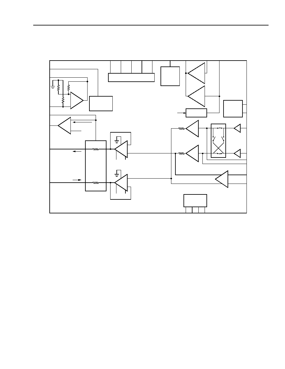
Architecture Diagram
12-3530.C (F)
Figure 1. Architecture Diagram
I
REF
VITR
TXI
ITR
VTX
PT
PR
ICM
TRGDET
CF2
CF1
FB2
FB1
POWER/BATTERY SWITCH
AGND
V
CC
BGND
V
BAT2
V
BAT1
I
PROG
NSTAT
RTFLT
DCOUT
REFERENCE
AAC
X20
(ITR/308)
TIP/RING
CURRENT
SENSE
ITR
ITR
RFT
18
RFR
18
V
BAT1
PARALLEL
DATA
INTERFACE
B0
B1
B2
B3
X1
X1
RCVN
RCVP
CURRENT
LIMIT
AND
INRUSH
CONTROL
RING
LOOP
RECTIFIER
VTX
COMMON-
MODE
CURRENT
DETECTOR
TRIP
CLOSURE
≠
+
9214A GAIN = 4
+
≠
+
≠
≠
+
GAIN
AX
9214G GAIN = 1
ac INTERFACE
CIRCUIT
V
BAT2
V
BAT1
V
BAT2
V
REF

Preliminary Data Sheet
October 2001
Low-Cost Ringing SLIC
L9214A/G
8
Agere Systems Inc.
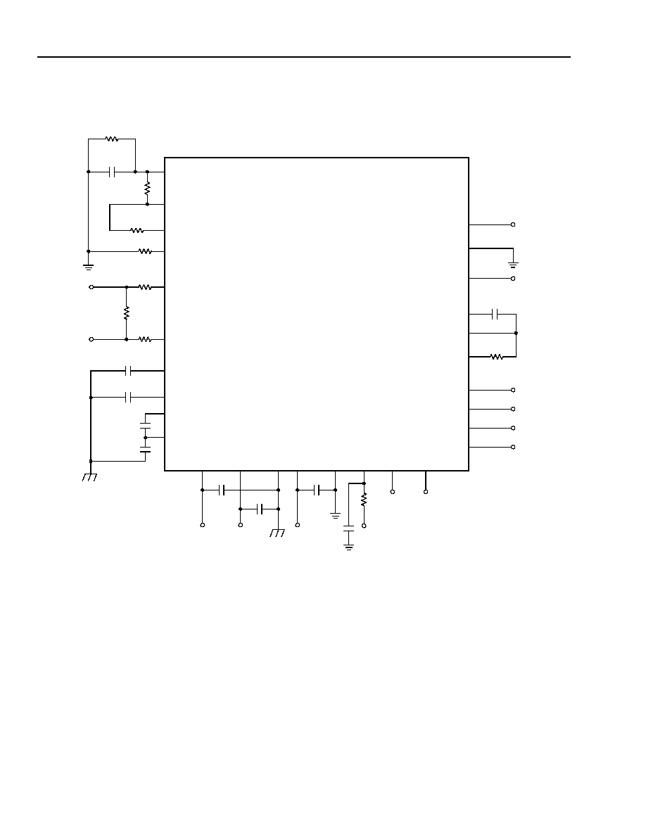
Pin Information
12-3568 (F)
Figure 2. 28-Pin SOG Diagram
Figure 3. 32-Pin PLCC Diagram
5
6
7
8
9
10
11
25
24
23
22
21
20
19
DCOUT
I
PROG
CF2
CF1
RTFLT
I
REF
AGND
B0
B1
B2
B3
FB1
PR
PT
L9214
4
RCVN
3
RCVP
2
VITR
1
NSTAT
26
ITR
27
VTX
28
TXI
12
V
CC
13
V
BAT1
14
V
BAT2
18
FB2
17
ICM
16
TRGDET
15
BGND
28-PIN SOG
1
4
30
5
13
21
29
14
20
3
2
31
32
28
27
26
25
24
23
22
15
16
17
18
19
12
11
10
9
8
7
6
I
RE
F
AG
ND
V
CC
V
BAT
1
V
BAT
2
BG
ND
TR
G
D
E
T
RTFLT
CF1
CF2
I
PROG
DCOUT
NC
NC
NC
RCVN
RCVP
VI
T
R
NC
NST
A
T
TX
I
VT
X
IT
R
ICM
FB2
FB1
PT
PR
B3
B2
B1
B0
L9214
32-PIN PLCC
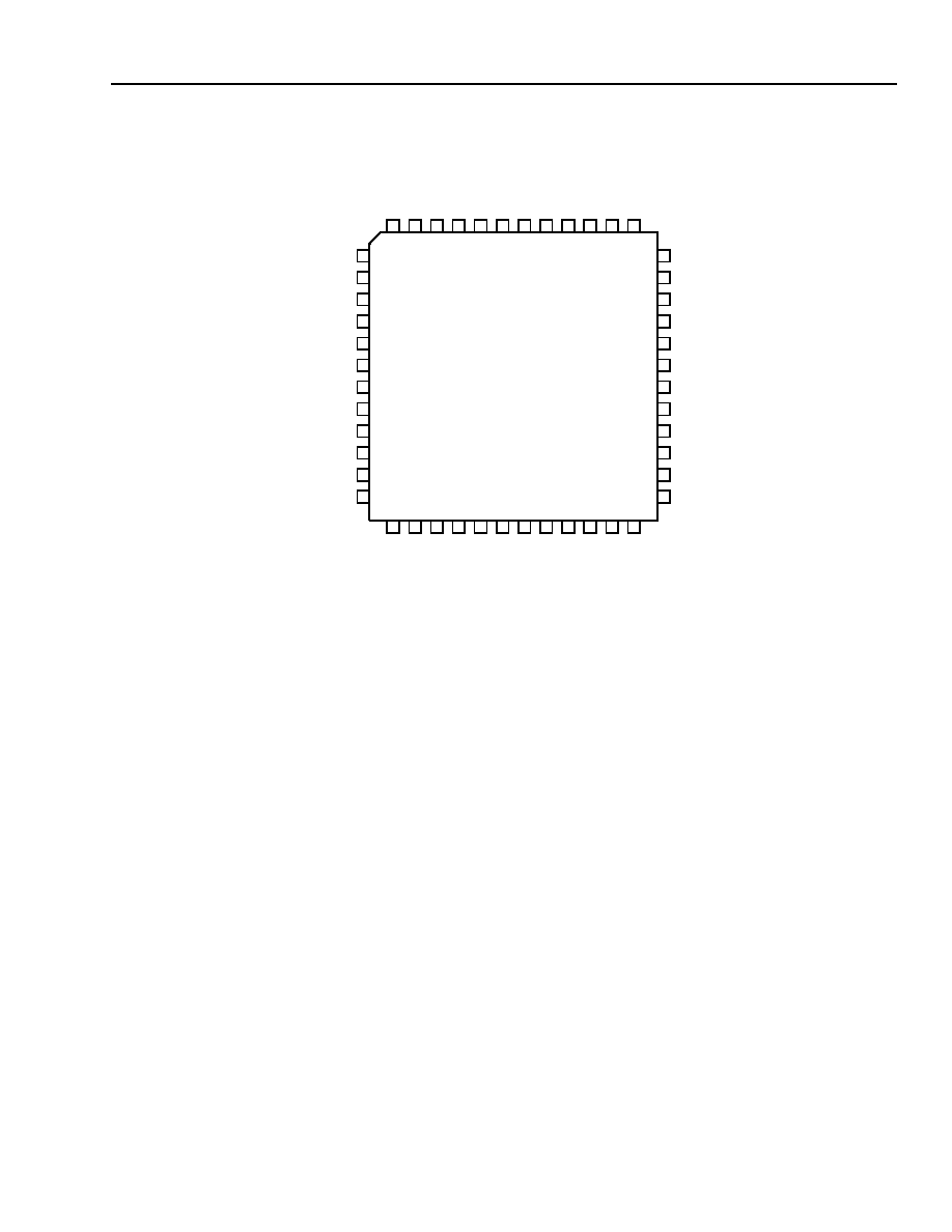
Preliminary Data Sheet
October 2001
Low-Cost Ringing SLIC
L9214A/G
Agere Systems Inc.
9
Pin Information
(continued)
12-3361f(F)
Figure 4. 48-Pin MLCC Diagram
1
3
4
6
7
8
9
10
11
12
2
48
46
45 44
43 42 41 40
38
37
47
13
16 17
18 19
20 21 22 23
24
14
36
33
32
31
30
29
28
27
26
25
35
B3
PT
FB1
NC
I
RE
F
NC
PR
RC
V
N
NC
RC
V
P
NC
NC
FB2
TR
G
D
E
T
NC
V
BA
T
2
VI
T
R
34
VT
X
39
15
5
NC
I
PROG
CF2
RTFLT
AG
ND
NC
IC
M
B2
B0
35
L9214A/G
48-PIN MLCC
DCOUT
CF1
B1
BG
ND
NC
NC
NC
NC
VCC
NC
NC
NC
NC
NC
NC
NC
IT
R
TX
I
NS
T
A
T
NC
V
BA
T
1

Preliminary Data Sheet
October 2001
Low-Cost Ringing SLIC
L9214A/G
10
Agere Systems Inc.
Pin Information
(continued)
Table 1. Pin Descriptions
28-Pin
SOG
32-Pin
PLCC
48-Pin
MLCC
Symbol Type
Name/Function
1
1
43
NSTAT
O
Loop Closure Detector Output--Ring Trip Detector
Output. When low, this logic output indicates that an off-
hook condition exists or ringing is tripped.
--
--
5, 14, 18,
28, 32, 39,
42, 44
NC
--
No Connection. May be used as a tie point.
--
2, 6, 7, 8
1--4, 8,
11, 17, 21,
27, 30, 37,
46
NC
--
No Connection. May not be used as a tie point.
2
3
45
VITR
O
Transmit ac Output Voltage. Output of internal AAC
amplifier. This output is a voltage that is directly propor-
tional to the differential ac tip/ring current.
3
4
47
RCVP
I
Receive ac Signal Input (Noninverting). This high-
impedance input controls to ac differential voltage on tip
and ring. This node is a floating input.
4
5
48
RCVN
I
Receive ac Signal Input (Inverting). This high-imped-
ance input controls to ac differential voltage on tip and
ring. This node is a floating input.
5
9
6
DCOUT
O
dc Output Voltage. This output is a voltage that is
directly proportional to the absolute value of the differen-
tial tip/ring current. This is used to set the dc current limit
and the ring trip threshold.
6
10
7
I
PROG
I
Current-Limit Program Input. A resistor is connected
from this pin to DCOUT to program the dc current limit for
the device.
7
11
9
CF2
--
Filter Capacitor. Connect a capacitor from this node to
ground.
8
12
10
CF1
--
Filter Capacitor. Connect a capacitor from this node to
CF2.
9
13
12
RTFLT
--
Ring Trip Filter. Connect this lead to DCOUT via a resis-
tor and to AGND with a capacitor or a resistor capacitor
combination, depending on the ringing type, to filter the
ring trip circuit to prevent spurious responses.
10
14
13
I
REF
I
SLIC Internal Reference Current. Connect a resistor
between this pin and AGND to generate an internal refer-
ence current.
11
15
15
AGND
GND
Analog Signal Ground.
12
16
16
V
CC
PWR
Analog Power Supply. User choice of 5 V or 3.3 V nom-
inal power supply.
13
17
19
V
BAT1
PWR
Battery Supply 1. High-voltage battery.
14
18
20
V
BAT2
PWR
Battery Supply 2. Low-voltage battery or power control
resistor.
15
19
22
BGND
GND
Battery Ground. Ground return for the battery supplies.

Preliminary Data Sheet
October 2001
Low-Cost Ringing SLIC
L9214A/G
Agere Systems Inc.
11
Pin Information
(continued)
Table 1. Pin Descriptions (continued)
28-Pin
SOG
32-Pin
PLCC
48-Pin
MLCC
Symbol Type
Name/Function
16
20
23
TRGDET
O
Tip/Ring Ground Detect. When high, this open collector
output indicates the presence of a ring ground or a tip
ground. This supervision output may be used in ground
key or common-mode fault detection applications.
17
21
24
ICM
I
Common-Mode Current Sense. To program tip or ring
ground sense threshold, connect a resistor to V
CC
and
connect a capacitor to AGND to filter 50/60 Hz. If unused,
the pin is connected to ground.
18
22
25
FB2
--
Polarity Reversal Slowdown Capacitor. Connect a
capacitor from this node for controlling rate of battery
reversal. Also used for ringing, this pin cannot be left
open.
19
23
26
FB1
--
Polarity Reversal Slowdown Capacitor. Connect a
capacitor from this node for controlling rate of battery
reversal. Also used for ringing, this pin cannot be left
open.
20
24
29
PT
I/O
Protected Tip. The input to the loop sensing circuit and
output drive of the tip amplifier. Connect to loop through
overvoltage and overcurrent protection.
21
25
31
PR
I/O
Protected Ring. The input to the loop sensing circuit and
output drive of the ring amplifier. Connect to loop through
overvoltage and overcurrent protection.
22
26
33
B3
I
State Control Input.
23
27
34
B2
I
State Control Input.
24
28
35
B1
I
State Control Input.
25
29
36
B0
I
State Control Input.
26
30
38
ITR
I
Transmit Gain. Input to AX amplifier. Connect a resistor
from this node to VTX to set transmit gain. Gain shaping
for termination impedance with a COMBO I codec is also
achieved with a network from this node to VTX.
27
31
40
VTX
O
ac/dc Output Voltage. Output of internal AX amplifier.
The voltage at this pin is directly proportional to the differ-
ential tip/ring current.
28
32
41
TXI
I
ac/dc Separation. Input to internal AAC amplifier. Con-
nect a 0.1
µ
F capacitor from this pin to VTX.

Preliminary Data Sheet
October 2001
Low-Cost Ringing SLIC
L9214A/G
12
Agere Systems Inc.
Operating States
Table 2. Control States
* In this state, all supervision functions are disabled, on hook transmission is disabled, pin PT is positive with respect to PR, V
BAT1
is applied to
tip/ring, and the tip to ring voltage will be equivalent to the scan state.
B3
B2
B1
B0
State
0
0
0
0
Disconnect
0
0
0
1
Ringing, (line reverse with high slope)
0
0
1
0
Unused*
0
0
1
1
Ringing, (line forward with high slope)
0
1
0
0
Disconnect
0
1
0
1
Reverse active and on-hook, fast polarity reversal
0
1
1
0
Scan
0
1
1
1
Forward active and on-hook, fast polarity reversal
1
0
0
0
Disconnect
1
0
0
1
Ringing, (line reverse with low slope)
1
0
1
0
Unused*
1
0
1
1
Ringing, (line forward with low slope)
1
1
0
0
Disconnect
1
1
0
1
Reverse active and on-hook, slow polarity reversal
1
1
1
0
Scan
1
1
1
1
Forward active and on-hook, slow polarity reversal
State Definitions
Forward Active (Fast Polarity Reversal)
Off-hook
s
Pin PT is positive with respect to PR.
s
V
BAT2
is applied to tip/ring drive amplifiers for the
majority of loop lengths. This may also be derived
from V
BAT1
through a power control resistor.
s
Loop closure and common-mode detect are active.
s
Ring trip detector is turned off to conserve power.
s
Overhead is set for undistorted transmission of
+3.17 dBm into 600
.
On-hook
s
Pin PT is positive with respect to PR.
s
V
BAT1
is applied to tip/ring drive amplifiers. The tip to
ring on-hook differential voltage will be between
≠42.5 V and ≠56.5 V with a primary battery of ≠65 V.
s
Loop closure and common-mode detect are active.
s
Ring trip detector is turned off to conserve power.
s
On-hook transmission is enabled.
s
Overhead is set to nominal 17.0 V for undistorted
transmission of 0 dBm into 600
.
Forward Active (Slow Polarity Reversal)
Off-hook
s
Same as the forward active (fast polarity reversal)
state, but with slower polarity reversal.
On-hook
s
Same as the forward active (fast polarity reversal)
state, but with slower polarity reversal.

Preliminary Data Sheet
October 2001
Low-Cost Ringing SLIC
L9214A/G
Agere Systems Inc.
13
State Definitions
(continued)
Reverse Active (Fast Polarity Reversal)
Off-hook
s
Pin PR is positive with respect to PT.
s
V
BAT2
is applied to tip/ring drive amplifiers via the soft
battery switch for the majority of loop lengths. This
may also be derived from V
BAT1
through a power
control resistor.
s
Loop closure and common-mode detect are active.
s
Ring trip detector is turned off to conserve power.
s
Overhead is set to nominal 4.0 V for undistorted
transmission of 0 dBm into 600
and may be
increased automatically for larger signal levels.
On-hook
s
Pin PR is positive with respect to PT.
s
V
BAT1
is applied to tip/ring drive amplifiers. The tip to
ring on-hook differential voltage will be between
≠42.5 V and ≠56.5 V with a primary battery of ≠65 V.
s
Loop closure and common-mode detect are active.
s
Ring trip detector is turned off to conserve power.
s
On-hook transmission is enabled.
s
Overhead is set to nominal 17.0 V for undistorted
transmission of 0 dBm into 600
.
Reverse Active (Slow Polarity Reversal)
Off-hook
s
Same as the reverse active (fast polarity reversal)
state, but with slower polarity reversal.
On-hook
s
Same as the reverse active (fast polarity reversal)
state, but with slower polarity reversal.
Scan
s
Except for loop closure, all circuits (including ring trip
and common-mode detector) are powered down.
s
On-hook transmission is disabled.
s
Pin PT is positive with respect to PR, and V
BAT1
is
applied to tip/ring.
s
The tip to ring on-hook differential voltage will be
between ≠42.5 V and ≠56.5 V with a ≠65 V primary
battery.
Disconnect
s
The tip/ring amplifiers and all supervision are turned
off.
s
The SLIC goes into a high-impedance state.
s
NSTAT is forced high (on-hook).
Ring
s
Ringing controlled digitally or by a PWM input signal
s
Power ring signal is applied to tip and ring.
s
Software-selectable slew rate, fast or slow.
s
Ring trip supervision and common-mode current
supervision are active; loop closure is inactive.
s
Overhead voltage is reduced to typically 2.5 V and
current limit set at I
PROG
is disabled.
s
Current is limited by saturation current of the amplifi-
ers themselves, typically 72 mA peak at 125 ∞C.
Thermal Shutdown
s
Not controlled via truth table inputs.
s
This mode is caused by excessive heating of the
device, such as may be encountered in an extended
power-cross situation.

Preliminary Data Sheet
October 2001
Low-Cost Ringing SLIC
L9214A/G
14
Agere Systems Inc.
Absolute Maximum Ratings
(at T
A
= 25 ∞C)
Stresses in excess of the absolute maximum ratings can cause permanent damage to the device. These are abso-
lute stress ratings only. Functional operation of the device is not implied at these or any other conditions in excess
of those given in the operational sections of the data sheet. Exposure to absolute maximum ratings for extended
periods can adversely affect device reliability.
Note: The IC can be damaged unless all ground connections are applied before, and removed after, all other connections. Furthermore, when
powering the device, the user must guarantee that no external potential creates a voltage on any pin of the device that exceeds the
device ratings. For example, inductance in a supply lead could resonate with the supply filter capacitor to cause a destructive overvoltage.
Table 3. Typical Operating Characteristics
Table 4. Thermal Characteristics
1. This parameter is not tested in production. It is guaranteed by design and device characterization.
2. Airflow, PCB board layers, and other factors can greatly affect this parameter.
Parameter
Symbol
Min
Typ
Max
Unit
dc Supply (V
CC
)
--
≠0.5
--
7.0
V
Battery Supply (V
BAT1
)
--
--
--
≠80
V
Battery Supply (V
BAT2
)
--
--
--
V
BAT1
V
Logic Input Voltage
--
≠0.5
--
V
CC
+ 0.5
V
Logic Output Voltage
--
≠0.5
--
V
CC
+ 0.5
V
Operating Temperature Range
--
≠40
--
125
∞C
Storage Temperature Range
--
≠40
--
150
∞C
Relative Humidity Range
--
5
--
95
%
Ground Potential Difference (BGND to AGND)
--
--
--
±1
V
Parameter
Min
Typ
Max
Unit
5 V dc Supplies (V
CC
)
--
5.0
5.25
V
3 V dc Supplies (V
CC
)
2.97
3.3
--
V
High Office Battery Supply (V
BAT1
)
≠63
≠65
≠70
V
Auxiliary Office Battery Supply (V
BAT2
)
≠15
≠21
V
BAT1
V
Operating Temperature Range (28-pin SOG)
0
25
70
∞C
Operating Temperature Range (32-pin PLCC)
≠40 25
85
∞C
Parameter
Min
Typ
Max
Unit
Thermal Protection Shutdown (T
jc
)
150
165
--
∞
C
28-pin SOG Thermal Resistance Junction to Ambient (
JA
)
1, 2
:
Natural Convection 2S2P Board
Wind Tunnel 200 Linear Feet per Minute (LFPM) 2S2P Board
--
--
70
59
--
--
∞
C/W
∞
C/W
32-pin PLCC Thermal Resistance Junction to Ambient (
JA
)
1, 2
:
Natural Convection 2S2P Board
Natural Convection 2S0P Board
Wind Tunnel 100 Linear Feet per Minute (LFPM) 2S2P Board
Wind Tunnel 100 Linear Feet per Minute (LFPM) 2S0P Board
--
--
--
--
35.5
50.5
31.5
42.5
--
--
--
--
∞
C/W
∞
C/W
∞
C/W
∞
C/W
48-pin MLCC Thermal Resistance Junction to Ambient (
JA
)
1, 2
--
38
--
∞
C/W
Preliminary Data Sheet
October 2001
Low-Cost Ringing SLIC
L9214A/G
Agere Systems Inc.
15
Electrical Characteristics
Table 5. Environmental Characteristics
1. Not to exceed 26 grams of water per kilogram of dry air.
Table 6. 5.0 V Supply Currents
V
BAT1
= ≠65 V, V
BAT2
= ≠21 V, V
CC
= 5.0 V.
Table 7. 5.0 V Powering
V
BAT1
= ≠65 V, V
BAT2
= ≠21 V, V
CC
= 5.0 V.
Note:
Refer to the power control description in the Applications section to calculate power dissipation in the forward/reverse off-hook state.
Parameter
Min
Typ
Max
Unit
Temperature Range (28-pin SOG)
0
--
70
∞C
Temperature Range (32-pin PLCC and 48-pin MLCC)
≠40
--
85
∞C
Humidity Range
1
5
--
95
1
%RH
Parameter
Min
Typ
Max
Unit
Supply Currents (scan state; no loop current):
I
VCC
I
VBAT1
I
VBAT2
--
--
--
2.90
0.09
0.04
3.80
0.20
0.07
mA
mA
mA
Supply Currents (forward/reverse active; no loop current, V
BAT1
applied):
I
VCC
I
VBAT1
I
VBAT2
--
--
--
4.8
1.5
1.0
6.00
1.95
1.20
mA
mA
mA
Supply Currents (disconnect mode):
I
VCC
I
VBAT1
I
VBAT2
--
--
--
1.60
0.02
0.01
2.20
0.10
0.02
mA
mA
mA
Supply Currents (ringing mode, no load applied):
I
VCC
I
VBAT1
I
VBAT2
--
--
--
4.40
1.70
0.57
5.0
2.2
0.7
mA
mA
mA
Parameter
Min
Typ
Max
Unit
Power Dissipation (scan state; no loop current)
--
21
33
mW
Power Dissipation (forward/reverse active; no loop current, V
BAT1
applied)
--
143
182
mW
Power Dissipation (disconnect mode)
--
10
18
mW
Power Dissipation (ring mode; no load applied)
--
144
183
mW
Preliminary Data Sheet
October 2001
Low-Cost Ringing SLIC
L9214A/G
16
Agere Systems Inc.
Electrical Characteristics
(continued)
Table 8. 3.3 V Supply Currents
V
BAT1
= ≠65 V, V
BAT2
= ≠21 V, V
CC
= 3.3 V.
Table 9. 3.3 V Powering
V
BAT1
= ≠65 V, V
BAT2
= ≠21 V, V
CC
= 3.3 V.
Note:
Refer to the power control description in the Applications section to calculate power dissipation in the forward/reverse off-hook state.
Parameter
Min
Typ
Max
Unit
Supply Currents (scan state; no loop current):
I
VCC
I
VBAT1
I
VBAT2
--
--
--
2.30
0.09
0.04
3.00
0.18
0.07
mA
mA
mA
Supply Currents (forward/reverse active; no loop current, V
BAT1
applied):
I
VCC
I
VBAT1
I
VBAT2
--
--
--
4.40
1.50
0.97
5.30
1.90
1.20
mA
mA
mA
Supply Currents (disconnect mode):
I
VCC
I
VBAT1
I
VBAT2
--
--
--
1.20
0.02
0.01
1.70
0.10
0.02
mA
mA
mA
Supply Currents (ringing mode, no load applied):
I
VCC
I
VBAT1
I
VBAT2
--
--
--
4.00
1.64
0.54
4.75
2.16
0.60
mA
mA
mA
Parameter
Min
Typ
Max
Unit
Power Dissipation (scan state; no loop current)
--
14
23
mW
Power Dissipation (forward/reverse active; no loop current, V
BAT1
applied)
--
132
166
mW
Power Dissipation (disconnect mode)
--
5
13
mW
Power Dissipation (ring mode; no loop current)
--
131
169
mW

Preliminary Data Sheet
October 2001
Low-Cost Ringing SLIC
L9214A/G
Agere Systems Inc.
17
Electrical Characteristics
(continued)
Table 10. Two-Wire Port
* Values guaranteed by design, not subject to production test.
Corresponds to 55 dB minimum with 1%, 30
resistors per Q552 (11/96) Section 2.1.2 and IEEE
Æ
455.
Parameter
Min
Typ
Max
Unit
Tip or Ring Drive Current = dc + Longitudinal + Signal Currents
72
--
--
mApeak
Tip or Ring Drive Current = Ringing + Longitudinal
37
--
--
mApeak
Signal Current
5
--
--
mArms
Longitudinal Current Capability per Wire (Longitudinal current is indepen-
dent of dc loop current.)
8.5
15
--
mArms
Ringing Current (R
LOAD
= 2330
+ 24
µ
F)
25
--
--
mApeak
Ringing Current (R
LOAD
= 3500
+ 1.8
µ
F)
12
--
--
mApeak
Ringing Current Limit (R
LOAD
= 100
)
--
--
90
mApeak
dc Loop Current--I
LIM
(R
LOOP
= 500
):
Programming Range (V
CC
= 5.0 V)
Programming Range (V
CC
= 3.3 V)
15
15
--
--
45
35
mA
mA
dc Current Variation (current limit 15 mA to 45 mA)
--
--
±10
%
dc Loop Current (R
LOOP
= 100
, on to off hook transition)
t < 20 ms
--
--
--
--
350
100
mApeak
mA
dc Loop Current (R
LOOP
= 100
, on to off hook transition)
t < 50 ms
--
--
--
--
--
150%
I
LIM
dc Feed Resistance, 2 x R
F
(excluding protection resistors)
25
36
50
Loop Resistance Range*, (0 dB overload into 600
)
I
LOOP
= 20 mA, V
BAT2
= ≠24 V, 50
(2 x R
F
), 60
(2 x R
P
), 300
R
LOOP
plus
Handset
I
LOOP
= 25 mA, V
BAT1
= ≠65 V, 50
(2 x R
F
), 60
(2 x R
P
), 1000
R
LOOP
plus Handset
840
1540
--
--
--
--
Open Loop Voltages, |V
BAT1
| = ≠63 V to ≠70 V:
Scan/On-Hook Transmission Mode:
|PT ≠ PR| ≠ Differential
|PT| or |PR| Referenced to BGND
42.5
--
48
--
--
56.5
V
V
Ring Mode, |V
BAT1
| = ≠63 V to ≠70 V:
|PT ≠ PR| ≠ Differential, (open loop ring voltage)
40
--
--
Vrms
Loop Closure Threshold:
Scan/Active/On-hook Transmission Modes
--
10
--
mA
Loop Closure Threshold Hysteresis:
--
2
--
mA
Ground Key:
Differential Detector Threshold
Detection
5
50
8
--
10
--
mA
ms
Longitudinal to Metallic Balance at PT/PR
Test Method per Figure 8, 1 kHz
58 dB minimum, 60 dB typical:
300 Hz to 600 Hz
600 Hz to 3.4 kHz
55
55
58
58
--
--
dB
dB
Metallic to Longitudinal (harm) Balance:
200 Hz to 1000 Hz
100 Hz to 4000 Hz
40
40
--
--
--
--
dB
dB
PSRR 500 Hz--3000 Hz:
V
BAT1
, V
BAT2
V
CC
(3.3 V operation)
40
25
--
--
--
--
dB
dB

Preliminary Data Sheet
October 2001
Low-Cost Ringing SLIC
L9214A/G
18
Agere Systems Inc.
Electrical Characteristics
(continued)
Table 11. Analog Pin Characteristics
Parameter
Min
Typ
Max
Unit
TXI (input impedance)
--
100
--
k
Output Offset (VTX)
Output Offset (VITR)
Output Drive Current (VTX)
Output Drive Current (VITR)
Output Voltage Swing (VTX) (V
CC
= 5.0 V)
Output Voltage Swing (VITR) (V
CC
= 5.0 V)
Output Short-circuit Current (VTX)
Output Short-circuit Current (VITR)
Output Load Resistance (VTX and VITR)
Output Load Capacitance (VTX)
Output Load Capacitance (VITR)
--
--
--
--
±3.7
--
--
--
10
--
--
±5
±70
±500
±250
--
--
±5
±6
--
--
--
--
--
--
--
+5/≠8
±3.1
--
--
--
20
50
mV
mV
µ
A
µ
A
V
V
mA
mA
k
pF
pF
RCVN and RCVP:
Input Voltage Range (V
CC
= 5.0 V)
Input Voltage Range (V
CC
= 3.3 V)
Input Bias Current
0
0
--
--
--
--
V
CC
≠ 0.5
V
CC
≠ 0.3
±1.5
V
V
µ
A

Preliminary Data Sheet
October 2001
Low-Cost Ringing SLIC
L9214A/G
Agere Systems Inc.
19
Electrical Characteristics
(continued)
Table 12. ac Feed Characteristics
1. Set externally either by discrete external components or a third- or fourth-generation codec. Any complex impedance R1 + R2 || C between
150
and 1400
can be synthesized.
2. This parameter is not tested in production. It is guaranteed by design and device characterization.
3. VITR transconductance depends on the resistor from ITR to VTX. This gain assumes an ideal 4750
, the recommended value. Positive cur-
rent is defined as the differential current flowing from PT to PR.
4. Tested per Figure 9. The gain reading is adjusted by the ratio of 696/660 to account for the 36
nominal ac feed resistance.
Parameter
Min
Typ
Max
Unit
ac Termination Impedance
1
150
600
1400
Total Harmonic Distortion (200 Hz--4 kHz)
2
:
Off-hook
On-hook
--
--
--
--
0.3
1.0
%
%
Transmit Gain (f = 1004 Hz, 1020 Hz)
3
:
PT/PR Current to VITR
291
300
309
V/A
Receive Gain
4
(f = 1004 Hz to 1020 Hz):
RCVP or RCVN to PT--PR (gain of 8 option, L9214A)
RCVP or RCVN to PT--PR (gain of 2 option, L9214G)
7.6
1.9
8
2
8.4
2.1
--
--
Gain vs. Frequency (transmit and receive)
2
, 600
Termination
(Q.552), 1004 Hz, 1020 Hz reference:
200 Hz--300 Hz
300 Hz--3.4 kHz
3.4 kHz--3.6 kHz
3.6 kHz--20 kHz
20 kHz--266 kHz
≠0.30
≠0.05
≠1.50
≠3.00
--
0
0
0
≠0.1
--
0.05
0.05
0.05
≠0.05
≠2.0
dB
dB
dB
dB
dB
Gain vs. Level (transmit and receive)
2
, 0 dBV Reference (Q.552):
≠55 dB to +3.0 dB
≠0.05
0
0.05
dB
Idle-channel Noise (tip/ring) 600
Termination:
Psophometric
C-Message
3 kHz Flat
--
--
--
≠82
8
--
≠77
13
20
dBmp
dBrnC
dBrn
Idle-channel Noise (VTX) 600
Termination:
Psophometric
C-Message
3 kHz Flat
--
--
--
≠82
8
--
≠77
13
20
dBmp
dBrnC
dBrn

Preliminary Data Sheet
October 2001
Low-Cost Ringing SLIC
L9214A/G
20
Agere Systems Inc.
Electrical Characteristics
(continued)
Table 13. Logic Inputs and Outputs (V
CC
= 5.0 V)
Table 14. Logic Inputs and Outputs (V
CC
= 3.3 V)
Table 15. Ringing Specifications
1. Voltage is measured across both resistive and capacitive elements of the ringer load.
2. Voltage is measured only across the resistive element of the ringer load.
Parameter
Symbol
Min
Typ
Max
Unit
Input Voltages:
Low Level
High Level
V
IL
V
IH
≠0.5
2.0
0.4
2.4
0.7
V
CC
V
V
Input Current:
Low Level (V
CC
= 5.25 V, V
I
= 0.4 V)
High Level (V
CC
= 5.25 V, V
I
= 2.4 V)
I
IL
I
IH
--
--
--
--
±250
±250
µ
A
µ
A
Output Voltages (open collector with internal pull-up resistor):
Low Level (V
CC
= 4.75 V, I
OL
= 200
µ
A)
High Level (V
CC
= 4.75 V, I
OH
= ≠10
µ
A)
V
OL
V
OH
0
2.4
0.2
--
0.4
V
CC
V
V
Parameter
Symbol
Min
Typ
Max
Unit
Input Voltages:
Low Level
High Level
V
IL
V
IH
≠0.5
2.0
0.2
2.5
0.5
V
CC
V
V
Input Current:
Low Level (V
CC
= 3.46 V, V
I
= 0.4 V)
High Level (V
CC
= 3.46 V, V
I
= 2.4 V)
I
IL
I
IH
--
--
--
--
±250
±250
µ
A
µ
A
Output Voltages (open collector with internal pull-up resistor):
Low Level (V
CC
= 3.13 V, I
OL
= 200
µ
A)
High Level (V
CC
= 3.13 V, I
OH
= ≠5
µ
A)
V
OL
V
OH
0
2.2
0.2
--
0.5
V
CC
V
V
Parameter
Min
Typ
Max
Unit
Ring Signal Isolation:
PT/PR to VITR
Ring Mode
--
60
--
dB
Ringing Voltage (5 REN 1386
+ 40 µF load, 200
loop, 2 x 30
protection
resistors, ≠69 V battery, 1.2 crest factor)
1
40
--
--
Vrms
Ringing Voltage (3 REN 2330
+ 24 µF load, 600
loop, 2 x 30
protection
resistors, ≠69 V battery, 1.2 crest factor)
1
40
--
--
Vrms
Ringing Voltage (2 REN 3500
+ 16 µF load, 1000
loop, 2 x 30
protec-
tion resistors, ≠69 V battery, 1.2 crest factor)
1
40
--
--
Vrms
Ringing Voltage (2 REN 3500
+ 1.8 µF load, 500
loop, 2 x 30
protection
resistors, ≠69 V battery, 1.2 crest factor)
2
40
--
--
Vrms
Ring Signal Distortion:
5 REN 1386
, 40 µF Load, 200
Loop
3 REN 2330
, 24 µF Load, 600
Loop
2 REN 3500
, 16 µF Load, 1000
Loop
2 REN 3500
, 1.8 µF Load, 500
Loop
--
--
--
--
5
5
5
5
--
--
--
10
%
%
%
%

Preliminary Data Sheet
October 2001
Low-Cost Ringing SLIC
L9214A/G
Agere Systems Inc.
21
Electrical Characteristics
(continued)
Table 16. Ring Trip (3 REN Configuration)
Ringing will not be tripped by the following loads:
s
100
resistor in series with a 2 µF capacitor applied across tip and ring. Ring frequency = 17 Hz to 23 Hz.
s
10 k
resistor in parallel with a 4 µF capacitor applied across tip and ring. Ring frequency = 17 Hz to 23 Hz.
Table 17. Ring Trip (5 REN Configuration)
Ringing will not be tripped by the following loads:
s
100
resistor in series with a 2 µF capacitor applied across tip and ring. Ring frequency = 17 Hz to 23 Hz.
s
10 k
resistor in parallel with a 6 µF capacitor applied across tip and ring. Ring frequency = 17 Hz to 23 Hz.
Note: Refer to the application section for further description of the 3 REN configuration vs. 5 REN configuration.
Parameter Min
Typ
Max
Unit
Ring Trip (NSTAT = 0): Loop Resistance (total)
0
--
1000
Ring Trip (NSTAT = 1): Loop Resistance (total)
10
--
--
k
Ringer Load
--
--
2330
+ 24
µ
F
--
Trip Time (f = 20 Hz)
--
--
130
ms
Parameter Min
Typ
Max
Unit
Ring Trip (NSTAT = 0): Loop Resistance (total)
0
--
600
Ring Trip (NSTAT = 1): Loop Resistance (total)
10
--
--
k
Ringer Load
--
--
1386
+ 40
µ
F
--
Trip Time (f = 20 Hz)
--
--
150
ms
Preliminary Data Sheet
October 2001
Low-Cost Ringing SLIC
L9214A/G
22
Agere Systems Inc.
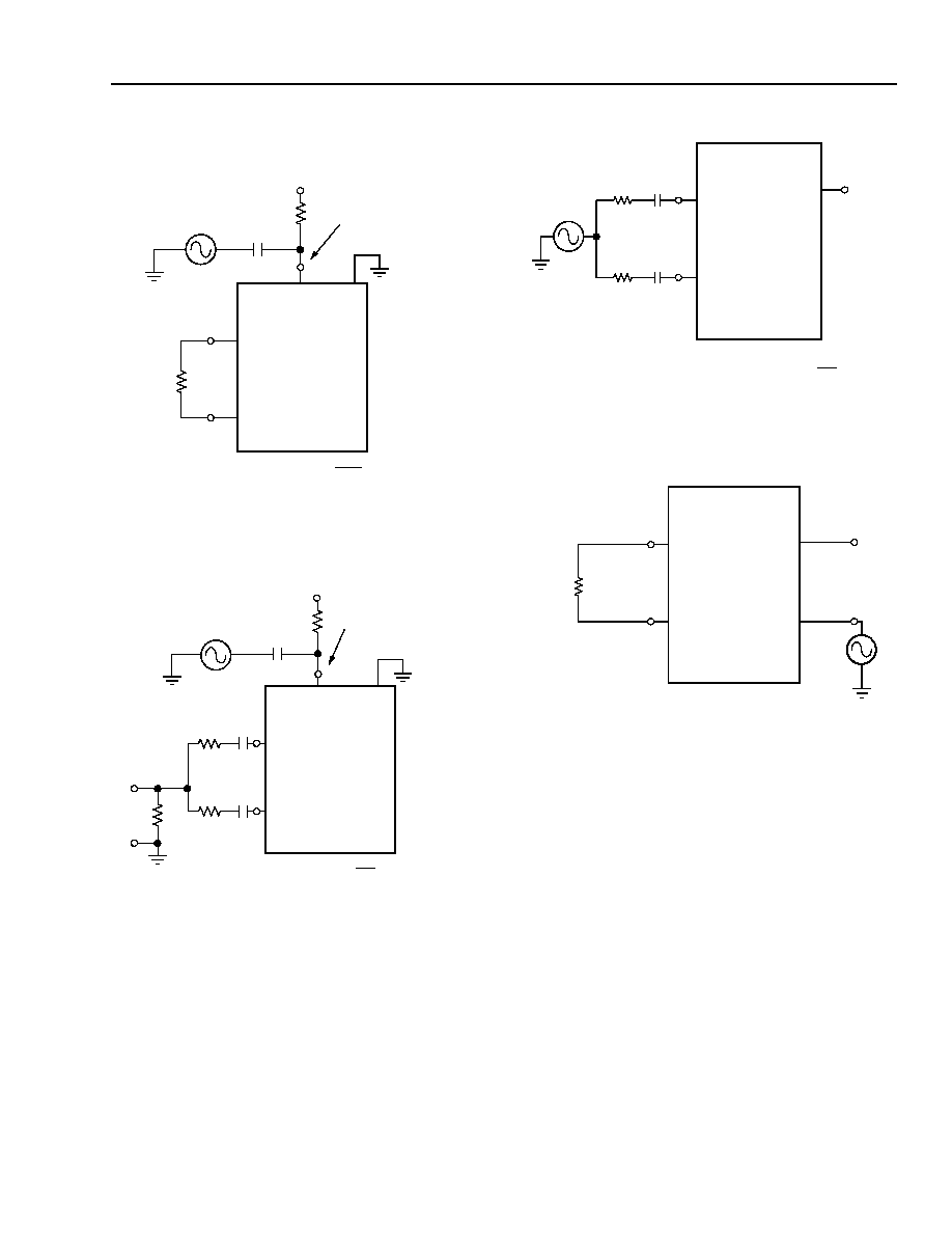
Test Configurations
12-3531.j (F)
Figure 5. Basic Test Circuit, V
CC
= 3.3 V (3 REN Configuration)
V
BAT2
V
BAT1
BGND V
CC
AGND
ICM TRGDET
0.1
µ
F
0.1
µ
F
0.1
µ
F
RTFLT
DCOUT
PR
PT
30
30
CF1
CF2
B0
B1
B2
B3
0.1
µ
F
VITR
RCVP
RCVN
ITR
VTX
TXI
V
BAT2
V
BAT1
V
CC
R
LOOP
100
/
600
TIP
RING
FB2
FB1
0.47
µ
F
L9214
NSTAT
B0
B1
B2
B3
4750
0.1
µ
F
600 k
0.1
µ
F
V
CC
I
PROG
I
REF
28.7 k
5.76 k
75 k
133 k
1
µ
F
0.047
µ
F
0.047
µ
F
RCVP
RCVN
VITR
Preliminary Data Sheet
October 2001
Low-Cost Ringing SLIC
L9214A/G
Agere Systems Inc.
23
Test Configurations
(continued)
12-2582.c (F)
Figure 6. Metallic PSRR
12-2583.b (F)
Figure 7. Longitudinal PSRR
12-2584.D (F)
Figure 8. Longitudinal Balance
12-2587.J (F)
Figure 9. ac Gains
V
S
4.7
µ
F
100
V
BAT
OR
V
CC
DISCONNECT
V
T/R
V
BAT
OR
V
CC
TIP
RING
BASIC
TEST CIRCUIT
+
≠
PSRR = 20log
V
S
V
T/R
600
BYPASS CAPACITOR
V
S
4.7
µ
F
100
V
BAT
OR
V
CC
DISCONNECT
BYPASS CAPACITOR
56.3
V
BAT
OR V
CC
TIP
RING
BASIC
TEST CIRCUIT
PSRR = 20log
V
S
V
M
67.5
10
µ
F
10
µ
F
67.5
V
M
+
≠
TIP
RING
BASIC
TEST CIRCUIT
LONGITUDINAL BALANCE = 20log
V
S
VITR
368
100
µ
F
100
µ
F
368
V
S
VITR
PT
PR
BASIC
TEST CIRCUIT
600
V
T/R
+
≠
RCVN
V
S
VITR
RCVN
OR
RCVP
OR
RCVP
G
X MT
V
XM T
V
T R
/
-------------
=
G
R CV
V
T R
/
V
R CV P
OR V
RC V N
-------------------------------------------------
=

Preliminary Data Sheet
October 2001
Low-Cost Ringing SLIC
L9214A/G
24
Agere Systems Inc.
Applications
Power Control
Under normal device operating conditions, power dissi-
pation must be controlled to prevent the device temper-
ature from rising too close to the thermal shutdown
point. Power dissipation is highest with higher battery
voltages, higher current limit, and under shorter dc loop
conditions. Additionally, higher ambient temperature
will reduce thermal margin. Increasing the number of
PC board layers and increasing airflow around the
device are typical ways of improving thermal margin.
The maximum recommended junction temperature for
the L9214 is 150 ∞C. The junction temperature is:
Tj = T
AMBIENT
+
JA
* P
SLIC
The thermal impedance of this device depends on the
package type as well as number of PCB layers and air-
flow. The thermal impedance of the 28-pin SOG pack-
age is somewhat higher than the 32-pin PLCC
package. The 28-pin SOG package in still air with a
single-sided PCB is rated at 70 ∞C/W. The 32-pin
PLCC package thermal impedance with no airflow on a
four-layer PCB is estimated at 37 ∞C/W.
The power handling capability of the package is:
P
SLIC
= (150 ∞C ≠ T
AMBIENT
)/
JA
which is a minimum of 0.93 W for the 28-pin SOG
package with a single-sided PCB and no airflow and as
much as 2.15 W for the 32-pin PLCC package with a
multilayer PCB.
This device is intended to operate with a high-voltage
primary battery of ≠63 V to ≠70 V. Under short-loop
conditions, an internal soft battery switch shunts most
(all but I
BIAS
= 3.5 mA) of the loop current to an auxiliary
battery of lower absolute voltage (typically ≠21 V).
Where single battery operation is required, an external
power control resistor can be connected from the V
BAT2
pin to V
BAT1
and all but 3.5 mA of the loop current will
flow through the power control resistor.
The power dissipated in the device is best illustrated by
an example. Assume V
BAT1
is ≠65 V, V
BAT2
is ≠21 V,
and the current limit is is I
LOOP
.
Let I
Q1
and I
Q2
be the quiescent currents drawn from
V
BAT1
and V
BAT2
respectively (the current drawn from
the battery when the phone is on-hook). Let I
BIAS
be
the additional current drawn from V
BAT1
when the
phone is off-hook.
I
BIAS
= I
VBAT1(off-hook)
≠ I
Q1
Typically I
BIAS
is 3.5 mA. This additional V
BAT1
current
contributes to the loop current and the remaining loop
current is supplied by V
BAT2
, so that
I
VBAT2
= I
Q2
+ I
LOOP
≠ I
BIAS
I
VCC
is the current drawn from V
CC
and is relatively con-
stant as the phone goes off hook.
The total power from the power supplies is:
P
TOTAL
= {[(I
Q1
+ I
BIAS
) * V
BAT1
] + [(I
Q2
+ I
LOOP
≠ I
BIAS
) *
V
BAT2
] + [(I
VCC
) * V
CC
]}
The maximum values of I
Q1
and I
Q2
are 1.95 mA and
1.20 mA respectively from Table 4.
If the current limit is set to 25 mA, given the current limit
tolerance of 10%, the maximum current limit is
27.5 mA. Also, assume 20
of wire resistance, 30
of protection resistance, and 200
for the handset
P
TOTAL
= {[(1.95 mA + 3.5 mA) * (65 V)] + [(1.20 mA +
27.5 mA ≠ 3.5 mA) * (21 V)] + [(6 mA) * (5 V)]
= 913.45 mW
The power delivered to the loop and the protection
resistors (P
LOOP
) is:
P
LOOP
= {(I
LOOP
)
2
* [(2 * R
PROTECTION
) + (R
WIRE
) +
(R
PHONE
)]} = {(27.5 mA)
2
* [(2 * 30
) + (20
) +
200
)]} = 212 mW
Thus, the total power dissipated by the SLIC is:
P
D
of SLIC = Total power (P
TOTAL
) ≠ power delivered to
loop and protection resistors (P
LOOP
).
P
D
= 913.45 mW ≠ 212 mW
= 701.45 mW for this example.
Since the minimum power handling capability of the
28-pin SOG package is 0.93 W, in this case either
package type is acceptable even with a single-sided
PCB. At higher battery voltages, higher ambient tem-
perature, and higher current limit, the required thermal
impedance drops and the 32-pin PLCC package, more
PCB layers, or some airflow might be required.
Another case to consider is the case of the power con-
trol resistor. In this case, the effective V
BAT2
voltage is:
V
BAT2
= V
BAT1
≠ R
PWR
* (I
LOOP
≠ I
BIAS
+ I
Q2
)
For the case of the 27.5 mA maximum current limit,
choosing R
PWR
= 1.75 k
would give V
BAT2
= ≠21 V and
the same SLIC power as above. The power in the
resistor would be:
P
RPWR
= (I
LOOP
≠ I
BIAS
+ I
Q2
)
2
* R
PWR
= 1.11 W
Choosing a larger R
PWR
would result in lower V
BAT2
and
lower SLIC power, but more power in the resistor. Simi-
larly, choosing a smaller R
PWR
results in higher V
BAT2
,
higher SLIC power, and less power in the resistor.

Preliminary Data Sheet
October 2001
Low-Cost Ringing SLIC
L9214A/G
Agere Systems Inc.
25
Applications
(continued)
dc Loop Current Limit
In the active modes, dc current limit is programmable
via an external resistor. The resistor is connected
between I
PROG
and DCOUT. The loop current limit
(I
LOOP
) with 100
load is related to the R
IPROG
pro-
gramming resistor by:
I
LOOP
(mA) = 4 mA/k
* R
IPROG
(k
) + 2 mA
Note that the overall current-limit accuracy achieved
will be affected by the specified accuracy of the internal
SLIC current-limit circuit and the accuracy of the exter-
nal resistor.
The above equation describes the active mode steady-
state current-limit response. There will be a transient
response of the current-limit circuit upon an on- to off-
hook transition. Typical active mode transient current-
limit response is given in Table 18.
Table 18. Typical Active Mode On- to Off-Hook Tip/
Ring Current-Limit Transient Response
Overhead Voltage
Active Mode
The overhead is preprogrammed in the active mode.
Note that overhead is not symmetrical with respect to
tip and ring. Under default conditions, the tip to ground
voltage is 2.1 V to 2.6 V and the ring to battery over-
head is 14.5 V typical.
The default overhead provides sufficient headroom for
on-hook transmission of a +3.17 dBm signal into
600
.
+3.17 dBm = 10 log (Vrms
2
/ P
0
* R
600
)
dBm = 10 log (Vrms
2
/ 0.001 W * 600
)
+3.17 dBm = 10 log
Vrms
= 1.12 V and Vpeak = 1.58 V are supported.
Scan Mode
If the magnitude of the primary battery is greater than
a nominal ≠63 V, the magnitude of the open-loop tip
to ring voltage is clamped to between ≠42.5 V and
≠56.5 V.
Again, the overhead is not symmetrical with respect to
tip and ring. With the magnitude of the primary battery
greater than a nominal ≠63 V, the tip to ground voltage
is clamped between ≠0.1 V and ≠0.6 V and the ring to
ground voltage is clamped between ≠42.5 V and
≠56.5 V. If the magnitude of the primary battery is less
than a nominal ≠63 V, the tip to ground voltage is
≠0.1 V to ≠0.6 V and the ring to battery voltage is typi-
cally 17 V less than V
BAT1
.
On-Hook Transmission Mode
If the magnitude of the primary battery is greater than
63 V, the magnitude of the open-loop tip to ring voltage
will be greater than 42.5 V. If the magnitude of the pri-
mary battery is less than 63 V, the open-loop voltage
may be less than 42.5 V and is approximately 17 V less
than the magnitude of the primary battery voltage. For
primary battery voltages less than 70 V, the magnitude
of the ring to ground voltage will be less than 56.5 V.
Again, the overhead is not symmetrical with respect to
tip and ring. The tip voltage to ground is between ≠2 V
and ≠4.5 V and the ring to primary voltage is 14.5 V
typical.
Parameter
Value
Unit
dc Loop Current: Active Mode
R
LOOP
= 100
On- to Off-hook
Transition t < 20 ms
I
LOOP
+ 60
mA
dc Loop Current: Active Mode
R
LOOP
= 100
On- to Off-hook
Transition t < 30 ms
I
LOOP
+ 20
mA
dc Loop Current: Active Mode
R
LOOP
= 100
On- to Off-hook
Transition t < 50 ms
I
LOOP
mA
Vrms
2
0.6 IV
R
◊
(
)
--------------------------------

Preliminary Data Sheet
October 2001
Low-Cost Ringing SLIC
L9214A/G
26
Agere Systems Inc.
Applications
(continued)
Overhead Voltage
(continued)
Ring Mode
In the ring mode, to maximize ringing loop length, the
overhead is decreased to the saturation of the tip ring
drive amplifiers, a nominal 4 V. The tip to ground volt-
age is 1 V, and the ring to V
BAT1
voltage is 3 V.
The AX amplifier at VTX is active during the ring mode,
differential ring current may be sensed at VTX during
the ring mode.
Loop Range
The dc loop range for medium-loop applications is cal-
culated using:
The dc loop range for short-loop applications is calcu-
lated using:
where:
V
OHH
= 19.5 (2.5 V + 17 V) and
V
OHL
= 3.4 V (2.5 V + 0.9 V)
and where:
R
L
= loop resistance, not including protection resistors.
R
P
= protection resistor value.
Rdc = SLIC internal dc feed resistance.
|V
BAT1
| and |V
BAT2
| = battery voltage magnitude.
I
LOOP
= loop current.
V
OHH
= overhead voltage when power is drawn from
V
BAT1
.
V
OHL
= overhead voltage when power is drawn from
V
BAT2
.
The point of change over between V
BAT2
and V
BAT1
occurs at:
|V
BAT2
| ≠ (0.9 + 2.5) V > [(2R
P
+ R
DC
+ R
L
) * I
LOOP
] V
V
BAT2
is typically applied under off-hook conditions for
power conservation and SLIC thermal considerations.
The L9214 is intended for short- and medium-loop
applications and, therefore, will always be in current
limit during off-hook conditions. However, note that the
ringing loop length rather than the dc loop length will be
the factor to determine operating loop length. Where
V
BAT2
is insufficient to support the loop length, the
power will be taken from V
BAT1
.
Battery Reversal Rate
The rate of battery reverse is controlled or ramped by
capacitors FB1 and FB2. A chart showing FB1/FB2 val-
ues versus typical ramp time is given below. Leave
FB1 and FB2 open if it is not desired to ramp the rate of
battery reversal.
Table 19. FB1/FB2 Values vs. Typical Ramp Time at
V
BAT1
= ≠65 V
R
L
V
BAT1
V
OHH
≠
(
)
I
LOOP
-----------------------------------------------
2R
P
≠
R
dc
≠
=
R
L
V
BAT2
V
OHL
≠
(
)
I
LOOP
----------------------------------------------
2R
P
≠
R
dc
≠
=
C
FB1
/C
FB2
Transition Time
Fast, B3 = 0
Transition Time
Slow, B3 = 1
0.01
µ
F
7 ms
20 ms
0.1
µ
F
75 ms
220 ms
0.22
µ
F
145 ms
440 ms
0.47
µ
F
300 ms
900 ms
1.0
µ
F
600 ms
1.8 s
1.22
µ
F
750 ms
2.25 s
1.3
µ
F
830 ms
2.5 s
1.4
µ
F
900 ms
2.7 s
1.6
µ
F
1070 ms
3.2 s

Preliminary Data Sheet
October 2001
Low-Cost Ringing SLIC
L9214A/G
Agere Systems Inc.
27
Supervision
The L9214 offers the loop closure and ring trip supervi-
sion functions. Internal to the device, the outputs of
these detectors are multiplexed into a single package
output, NSTAT. Additionally, a common-mode current
detector for tip or ring ground detection is included for
ground key applications.
Loop Closure
The loop closure has a fixed typical 10 mA on- to off-
hook threshold in the active mode and a fixed 10 mA
on- to off-hook threshold from the scan mode. In either
case, there is a 2 mA hysteresis with V
CC
= 5.0 V and
with V
CC
= 3.3 V.
Ring Trip
The ring trip detector requires an external filter at the
input, minimizing external components. An R + R//C
combination of 75 k
and 133 k
//
1
µ
F, for a filter
pole at 3.3 Hz, is recommended for a 3 REN config-
uration. For a 5 REN configuration, a 150 k
and
100 k
//
1
µ
F (for a filter pole at 2.65 Hz) combination
is recommended.
The ring trip threshold is internally fixed and is indepen-
dent of battery voltage. The threshold, I
RT
= 20.1 mA.
Tip or Ring Ground Detector
In the ground key or ground start applications a com-
mon-mode current detector is used to indicate either a
tip- or ring-ground has occurred (ground key) or an off-
hook has occurred (ground start). The detection thresh-
old is set by connecting a resistor from ICM to V
CC
.
1000 * V
CC
/R
ICM
(k
) = I
TH
(mA)
where:
R
ICM
> 80 k
@ V
CC
= 3.3 V
R
ICM
> 150 k
@ V
CC
= 5.0 V
Additionally, a filter capacitor across R
ICM
will set the
time constant of the detector. No hysteresis is associ-
ated with this detector.
Power Ring
The device offers a ring mode, in which a power ring
signal is provided to the tip/ring pair. The standard
method of ringing is to perform trapezoidal ringing by
use of the state input pins. It is possible to select either
fast or slow slew rates to alter the crest factor of the
ringing signal. This allows designers to set the external
capacitors to a specific factor and change the ringing
frequency under software control while maintaining the
crest factor between 1.2 and 1.6 for the trapezoidal sig-
nal.
During the ring mode, it is also possible to supply a
pulse-width modulated, PWM, signal into the device's
B1 input. This signal is used to produce the power ring
signal. This signal must be removed during nonring
mode states. The user may input any crest factor ring
signal using this method; thus, the device will support a
sine wave (crest factor 1.414) or a lower or higher crest
factor input for increased power efficiency ring signal.
Various crest factors are shown below.
12-3346a (F)
Note: Slew rate = 5.65 V/ms; trise = tfall = 23 ms; pwidth = 2 ms;
period = 50 ms.
Figure 10. Ringing Waveform Crest Factor = 1.6
12-3347a (F)
Note: Slew rate = 10.83 V/ms; trise = tfall = 12 ms; pwidth = 13 ms;
period = 50 ms.
Figure 11. Ringing Waveform Crest Factor = 1.2
TIME (s)
≠80
≠60
≠40
≠20
0
20
40
60
80
0.00
0.02 0.06
0.04 0.08
0.10
0.12
0.14
0.16
0.18
0.20
VO
L
T
S
(V
)
TIME (s)
≠80
≠60
≠40
≠20
0
20
40
60
80
0.00
0.02 0.06
0.04 0.08
0.10
0.12
0.14
0.16
0.18
0.20
VO
L
T
S
(V
)
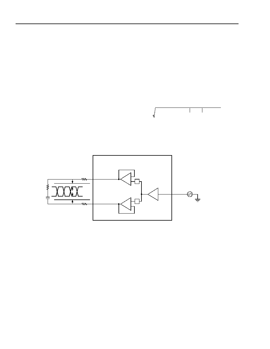
Preliminary Data Sheet
October 2001
Low-Cost Ringing SLIC
L9214A/G
28
Agere Systems Inc.
Supervision
(continued)
Power Ring
(continued)
The ring signal will appear balanced on tip and ring.
That is, the ring signal is applied on both tip and ring,
with the signal on tip 180
∞
out of phase from the signal
on ring. This operation is shown in Figure 12 below.
Ringing loop range is calculated as follows:
V
RINGLOAD
= {(V
BATTERY
≠ 4)/Crest Factor} *
{R
LOAD
/(R
LOAD
+ R
LOOP
+ 2 x R
PROTECTION
)}
As a practical example, calculate the maximum dc loop
length, assuming the following conditions:
Minimum required ring voltage = 40 Vrms
V
BATTERY
= ≠67 V
Trapezoidal ringing, crest factor = 1.2
Protection resistors = 30
each
Ring Load = 2 North American REN = 3500
+ 16
µ
F
Ringing frequency = 25 Hz
First, calculate the equivalent ringing load resistance at
25 Hz.
R
LOAD
= {(3500
)
2
+ (2 *
* 25 * 16E≠6)
≠2
}
0.5
R
LOAD
= 3522
40 Vrms = {(67 ≠ 4)/1.2)} {3522
/(R
LOOP
+ 3522
+
60
)}
R
LOOP
= 1040
Effects such as power supply tolerance and crest factor
tolerance can affect this calculation.
Crest factor is estimated by the formula:
Where:
f = ringing frequency; C
FB
= (C
FB1
+ C
FB2
)/2;
Ics = 30
µ
A with B3 = 1 and 90
µ
A with B3 = 0;
V
OHH
= 4 V
1
1
4
f
C
FB
V
BAT1
V
OHH
≠
)
◊
◊
◊
(
3
I
CS
◊
-----------------------------------------------------------------------------------------
≠
-------------------------------------------------------------------------------------------------------
=
12-3532.B (F)
Figure 12. Ring Operation
GND
V
BAT
RING
LOAD
1/2 R
LOOP
+ R
PROTECTION
1/2 R
LOOP
+ R
PROTECTION
PT
+1
PR
B1
SQUARE WAVE OR
PWM SIGNAL
L9214
V
TIP
V
RING
≠1
3 V
1 V

Preliminary Data Sheet
October 2001
Low-Cost Ringing SLIC
L9214A/G
Agere Systems Inc.
29
Periodic Pulse Metering (PPM)
Periodic pulse metering (PPM), also referred to as tele-
tax (TTX), is applied to the audio input of the L9214.
When in the active state, this signal is presented to the
tip/ring subscriber loop along with the audio signal. The
L9214 assumes that a shaped PPM signal is applied to
the audio
input.
ac Applications
ac Parameters
There are four key ac design parameters. Termination
impedance is the impedance looking into the 2-wire
port of the line card. It is set to match the impedance of
the telephone loop in order to minimize echo return to
the telephone set. Transmit gain is measured from the
2-wire port to the PCM highway, while receive gain is
done from the PCM highway to the transmit port.
Transmit and receive gains may be specified in terms
of an actual gain, or in terms of a transmission level
point (TLP), that is the actual ac transmission level in
dBm. Finally, the hybrid balance network cancels the
unwanted amount of the receive signal that appears at
the transmit port.
Codec Types
At this point in the design, the codec needs to be
selected. The interface network between the SLIC and
codec can then be designed. Below is a brief codec
feature summary.
First-Generation Codecs
These perform the basic filtering, A/D (transmit), D/A
(receive), and
µ
-law/A-law companding. They all have
an op amp in front of the A/D converter for transmit
gain setting and hybrid balance (cancellation at the
summing node). Depending on the type, some have
differential analog input and output stages, +5 V only or
±
5 V operation, and
µ
-law/A-law selectability. These
are available in single and quad designs. This type of
codec requires continuous time analog filtering via
external resistor/capacitor networks to set the ac
design parameters. An example of this type of codec is
the Agere T7504 quad 5 V only codec.
This type of codec tends to be the most economical in
terms of piece part price, but tends to require more
external components than a third-generation codec.
The ac parameters are fixed by the external R/C net-
work so software control of ac parameters is difficult.
Third-Generation Codecs
This class of devices includes all ac parameters set
digitally under microprocessor control. Depending on
the device, it may or may not have data control latches.
Additional functionality sometimes offered includes
tone plant generation and reception, PPM generation,
test algorithms, and echo cancellation. Again, this type
of codec may be 3.3 V, 5 V only, or
±
5 V operation, sin-
gle-, quad-, or 16-channel, and
µ
-law/A-law or 16-bit
linear coding selectable. Examples of this type of
codec are the Agere T8535/6 (5 V only, quad, standard
features), T8537/8 (3.3 V only, quad, standard fea-
tures), T8533/4 (5 V only, quad with echo cancellation),
and the T8531/32 (5 V only, eight- or 16-channel).
ac Interface Network
The ac interface network between the L9214 and the
codec will vary depending on the codec selected. With
a first-generation codec, the interface between the
L9214 and codec actually sets the ac parameters. With
a third-generation codec, all ac parameters are set dig-
itally, internal to the codec; thus, the interface between
the L9214 and this type of codec is designed to avoid
overload at the codec input in the transmit direction
and to optimize signal to noise ratio (S/N) in the receive
direction.
Because the design requirements are very different
with a first- or third-generation codec, the L9214 is
offered with two different receive gains. Each receive
gain was chosen to optimize, in terms of external com-
ponents required, the ac interface between the L9214
and codec.
With a first-generation codec, the termination imped-
ance is set by providing gain shaping through a feed-
back network from the SLIC VITR output to the SLIC
RCVN/RCVP inputs. The L9214 provides a transcon-
ductance from T/R to VITR in the transmit direction and
a single-ended to differential gain from either RCVN or
RCVP to T/R in the receive direction. Assuming a short
from VITR to RCVN or RCVP, the maximum imped-
ance that is seen looking into the SLIC is the product of
the SLIC transconductance times the SLIC receive
gain, plus the protection resistors. The various speci-
fied termination impedance can range over the voice-
band as low as 300
up to over 1000
. Thus, if the
SLIC gains are too low, it will be impossible to synthe-
size the higher termination impedances. Further, the
termination that is achieved will be far less than what is
calculated by assuming a short for SLIC output to SLIC
input.

Preliminary Data Sheet
October 2001
Low-Cost Ringing SLIC
L9214A/G
30
Agere Systems Inc.
ac Applications
(continued)
ac Interface Network
(continued)
In the receive direction, in order to control echo, the
gain is typically a loss, which requires a loss network at
the SLIC RCVN/RCVP inputs, which will reduce the
amount of gain that is available for termination imped-
ance. For this reason, a high-gain SLIC is required with
a first-generation codec.
With a third-generation codec, the line card designer
has different concerns. To design the ac interface, the
designer must first decide upon all termination imped-
ance, hybrid balances, and transmission level point
(TLP) requirements that the line card must meet. In the
transmit direction, the only concern is that the SLIC
does not provide a signal that is too hot and overloads
the codec input. Thus, for the highest TLP that is being
designed to, given the SLIC gain, the designer, as a
function of voiceband frequency, must ensure the
codec is not overloaded. With a given TLP and a given
SLIC gain, if the signal will cause a codec overload, the
designer must insert some sort of loss, typically a resis-
tor divider, between the SLIC output and codec input.
Note also that some third-generation codecs require
the designer to provide an inherent resistive termina-
tion via external networks. The codec will then provide
gain shaping, as a function of frequency, to meet the
return loss requirements. This feedback will increase
the signal at the codec input and increase the likeli-
hood that a resistor divider is needed in the transmit
direction. Further stability issues may add external
components or excessive ground plane requirements
to the design.
In the receive direction, the issue is to optimize the
S/N. Again, the designer must consider all the TLPs.
The idea is, for all desired TLPs, to run the codec at or
as close as possible to its maximum output signal, to
optimize the S/N. Remember noise floor is constant, so
the hotter the signal from the codec, the better the S/N.
The problem is if the codec is feeding a high-gain SLIC,
either an external resistor divider is needed to knock
the gain down to meet the TLP requirements, or the
codec is not operated near maximum signal levels,
thus compromising the S/N.
Thus, it appears that the solution is to have a SLIC with
a low gain, especially in the receive direction. This will
allow the codec to operate near its maximum output
signal (to optimize S/N), without an external resistor
divider (to minimize cost).
To meet the unique requirements of both type of
codecs, the L9214 offers two receive gain choices.
These receive gains are mask programmable at the
factory and are offered as two different code variations.
For interface with a first-generation codec, the L9214 is
offered with a receive gain of 8. For interface with a
third-generation codec, the L9214 is offered with a
receive gain of 2. In either case, the transconductance
in the transmit direction or the transmit gain is 300
,
(300 V/A).
This selection of receive gain gives the designer the
flexibility to maximize performance and minimize exter-
nal components, regardless of the type of codec cho-
sen.
Design Examples
First-Generation Codec ac Interface Network--
Resistive Termination
The following reference circuit shows the complete
SLIC schematic for interface to the Agere T7504 first-
generation codec for a resistive termination imped-
ance. For this example, the ac interface was designed
for a 600
resistive termination and hybrid balance
with transmit gain and receive gain set to 0 dBm. For
illustration purposes, no PPM injection was assumed in
this example.
This is a lower feature application example and uses
single battery operation, fixed overhead, current limit,
and loop closure threshold.
Resistor R
GN
is optional. It compensates for any mis-
match of input bias voltage at the RCVN/RCVP inputs.
If it is not used, there may be a slight offset at tip and
ring due to mismatch of input bias voltage at the
RCVN/RCVP inputs. It is very common to simply tie
RCVN directly to ground in this particular mode of oper-
ation. If used, to calculate RGN, the impedance from
RCVN to ac ground should equal the impedance from
RCVP to ac ground.
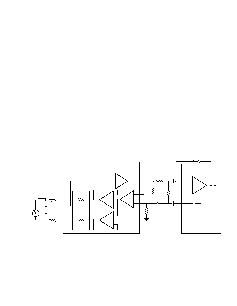
Preliminary Data Sheet
October 2001
Low-Cost Ringing SLIC
L9214A/G
Agere Systems Inc.
31
ac Applications
(continued)
Design Examples
(continued)
Example 1, Real Termination
The following design equations refer to the circuit in
Figure 13. Use these to synthesize real termination
impedance.
Termination Impedance:
z
T
=
Receive Gain:
V
T/R
I
T/R
≠
------------
z
T
36
2
+
R
P
2400
1
R
T 1
R
G P
---------
R
T 1
R
R C V
------------
+
+
-----------------------------------
+
=
g
rcv
V
T/R
V
FR
------------
=
g
rcv
8
1
R
R CV
R
T 1
-----------
R
R C V
R
G P
------------
+
+
1
Z
T
Z
T/R
---------
+
------------------------------------------------------------------
=
Transmit Gain:
Hybrid Balance:
h
bal
= 20log
h
bal
= 20log
To optimize the hybrid balance, the sum of the currents
at the VFX input of the codec op amp should be set to
0. The expression for ZHB becomes the following:
g
tx
V
GSX
V
T/R
-----------
=
g
t x
R
X
≠
R
T 2
---------
300
Z
T/R
---------
◊
=
R
X
R
HB
------------
g
tx
≠
g
rcv
◊
V
GSX
V
F R
---------------
R
H B
k
( )
R
X
g
tx
g
rcv
◊
-------------------
=
12-3569 (F)
Figure 13. ac Equivalent Circuit
R
P
Z
T
+
≠
R
P
V
T/R
I
T/R
V
S
Z
T/R
+
≠
RING
A
V
= ≠1
A
V
= 1
VITR
CURRENT
SENSE
TIP
+
≠
R
T1
R
RCV
R
HB1
R
T2
RCVN
RCVP
R
X
VGSX
VF
X
IN
V
FR
1/4 T7504 CODEC
R
GP
+2.4 V
≠0.300 V/mA
A
V
= 4
L9214
VF
X
IP
18
18
+
≠
+
≠
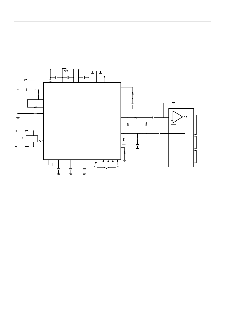
Preliminary Data Sheet
October 2001
Low-Cost Ringing SLIC
L9214A/G
32
Agere Systems Inc.
ac Applications
(continued)
Design Examples
(continued)
Example 1, Real Termination (continued)
12-3533.L (F)
Figure 14. Agere T7504 First-Generation Codec; Resistive Termination (5 REN Configuration)
V
BAT1
BGND
V
BAT2
V
CC
AGND ICM TRGDET
ground key
not used
C
VBAT1
0.1
µ
F
C
VBAT2
0.1
µ
F
C
CC
0.1
µ
F
PR
PT
AGERE
L7591
V
BAT1
FUSIBLE RESISTOR
30
30
CF1
CF2
FB1
FB2
NSTAT B3 B2 B1 B0
C
F1
0.22
µ
F
C
F2
0.1
µ
F
VITR
RCVP
RCVN
ITR
VTX
TXI
R
GX
4750
V
BAT1
V
BAT2
V
CC
C
TX
0.1
µ
F
1/4 T7504
CODEC
R
T6
C
C1
R
X
GSX
+2.4 V
R
HB1
VF
X
IN
R
RCV
R
T3
R
GP
C
C2
VF
R
O
DX
DR
FSE
FSEP
MCLK
ASEL
CONTROL
INPUTS
SYNC
AND
PCM
HIGHWAY
CLOCK
R
GN
≠
+
49.9 k
100 k
100 k
60.4 k
0.1
µ
F
17.65 k
26.7 k
69.8 k
0.1 µF
L9214A
FUSIBLE RESISTOR
OR PTC
OR PTC
RTFLT
DCOUT
I
PROG
(I
LOOP
= 25 mA)
I
REF
R
RT2
R
RT1
100 k
C
RT
1
µ
F
150 k
R
IPROG
5.76 k
R
IREF
28.7 k
C
FB1
0.01
µ
F
C
FB2
0.01
µ
F
FROM/TO
CONTROL
R
CR
5 k
C
CC1
150 nF
D
BAT1

Preliminary Data Sheet
October 2001
Low-Cost Ringing SLIC
L9214A/G
Agere Systems Inc.
33
ac Applications
(continued)
Design Examples
(continued)
Example 1, Real Termination (continued)
Table 20. L9214 Parts List for Agere T7504 First-Generation Codec; Resistive Termination
Note: T
X
= 0 dBm, R
X
= 0 dBm, termination impedance = 600
,
hybrid balance = 600
.
Name
Value
Tolerance
Rating
Function
Fault Protection
R
PT
30
1%
Fusible or PTC Protection resistor.
R
PR
30
1%
Fusible or PTC Protection resistor.
Protector
Agere
L7591
--
--
Secondary protection.
Power Supply
C
VBAT1
0.1
µ
F
20%
100 V
V
BAT
filter capacitor.
C
VBAT2
0.1
µ
F
20%
50 V
V
BAT
filter capacitor. |V
BAT2
| < |V
BAT1
|.
D
BAT1
1N4004
--
--
Reverse current.
C
CC
0.1
µ
F
20%
10 V
V
CC
filter capacitor.
C
F1
0.22
µ
F
20%
100 V
Filter capacitor.
C
F2
0.1
µ
F
20%
100 V
Filter capacitor.
dc Profile
R
IPROG
5.76 k
1%
1/16 W
With R
IREF
,
fixes dc current limit.
R
IREF
28.7 k
1%
1/16 W
With R
IPROG
,
fixes dc current limit.
Ringing/Ring Trip
C
RT
1.0
µ
F
20%
10 V
Ring trip filter capacitor.
R
RT1
100 k
1%
1/16 W
Ring trip filter resistor.
R
RT2
150 k
1%
1/16 W
Ring trip filter resistor.
C
FB1
0.01
µ
F
20%
100 V
With C
FB2
, slows rate of battery reversal. Sets crest factor
of balanced power ring signal.
C
FB2
0.01
µ
F
20%
100 V
With C
FB1
, slows rate of battery reversal. Sets crest factor
of balanced power ring signal.
ac Interface
R
GX
4750
1%
1/16 W
Sets T/R to VITR transconductance.
R
CR
5 k
5%
1/16 W
Compensation resistor.
C
CC1
150 pF
20%
10 V
Compensation capacitor.
C
TX
0.1
µ
F
20%
10 V
ac/dc separation.
C
C1
0.1
µ
F
20%
10 V
dc blocking capacitor.
C
C2
0.1
µ
F
20%
10 V
dc blocking capacitor.
R
T3
69.8 k
1%
1/16 W
With R
GP
and R
RCV
, sets termination impedance and
receive gain.
R
T6
49.9 k
1%
1/16 W
With R
X
, sets transmit gain.
R
X
100 k
1%
1/16 W
With R
T6
, sets transmit gain.
R
HB1
100 k
1%
1/16 W
With R
X
, sets hybrid balance.
R
RCV
60.4 k
1%
1/16 W
With R
GP
and R
T3
, sets termination impedance and
receive gain.
R
GP
26.7 k
1%
1/16 W
With R
RCV
and R
T3
, sets termination impedance and
receive gain.
R
GN
Optional
17.6 k
1%
1/16 W
Optional. Compensates for input offset at RCVN/RCVP.

Preliminary Data Sheet
October 2001
Low-Cost Ringing SLIC
L9214A/G
34
Agere Systems Inc.
ac Applications
(continued)
Design Examples
(continued)
First-Generation Codec ac Interface Network--
Complex Termination
The following reference circuit shows the complete
SLIC schematic for interface to the Agere T7504 first-
generation codec for the German complex termination
impedance. For this example, the ac interface was
designed for a 220
+ (820
|| 115 nF) complex ter-
mination and hybrid balance with transmit gain and
receive gain set to 0 dBm.
Complex Termination Impedance Design Example
The gain shaping necessary for a complex termination
impedance may be done by shaping across the Ax
amplifier at nodes ITR and VTX.
Complex termination is specified in the form:
5-6396(F)
To work with this application, convert termination to the
form:
5-6398(F)
where:
R
1
¥ = R
1
+ R
2
R
2
¥ =
(R
1
+ R
2
)
C¥ =
C
ac Interface Using First-Generation Codec
R
GX
/R
TGS
/C
GS
(Z
TG
): These components give gain
shaping to get good gain flatness. These components
are a scaled version of the specified complex termina-
tion impedance.
Note for pure (600
) resistive terminations, compo-
nents R
TGS
and C
GS
are not used. Resistor R
GX
is used
and is still 4750
.
R
X
/R
T6
: With other components set, the transmit gain
(for complex and resistive terminations) R
X
and R
T6
are
varied to give specified transmit gain.
R
T3
/R
RCV
/R
GP
: For both complex and resistive termina-
tions, the ratio of these resistors sets the receive gain.
For resistive terminations, the ratio of these resistors
sets the return loss characteristic. For complex termi-
nations, the ratio of these resistors sets the low-fre-
quency return loss characteristic.
C
N
/R
N1
/R
N2
: For complex terminations, these compo-
nents provide high-frequency compensation to the
return loss characteristic.
For resistive terminations, these components are not
used and RCVN is connected to ground via a resistor.
R
HB
: Sets hybrid balance for all terminations.
Set Z
TG
--gain shaping:
Z
TG
= R
GX
|| R
TGS
+ C
GS
which is a scaled version of
Z
T/R
(the specified termination resistance) in the
R
1
¥ || R
2
¥ + C¥ form.
R
GX
must be 4750
to set SLIC transconductance to
300 V/A.
R
GX
= 4750
At dc, C
GS
and C¥ are open.
R
GX
= M x R
1
¥
where M is the scale factor.
M =
It can be shown:
R
TGS
= M x R
2
¥
and
C
TGS
=
R
2
C
R
1
R
1
¥
C¥
R
2
¥
R
1
R
2
-------
R
2
R
1
R
2
+
---------------------
2
4750
R
1
--------------
C
M
------
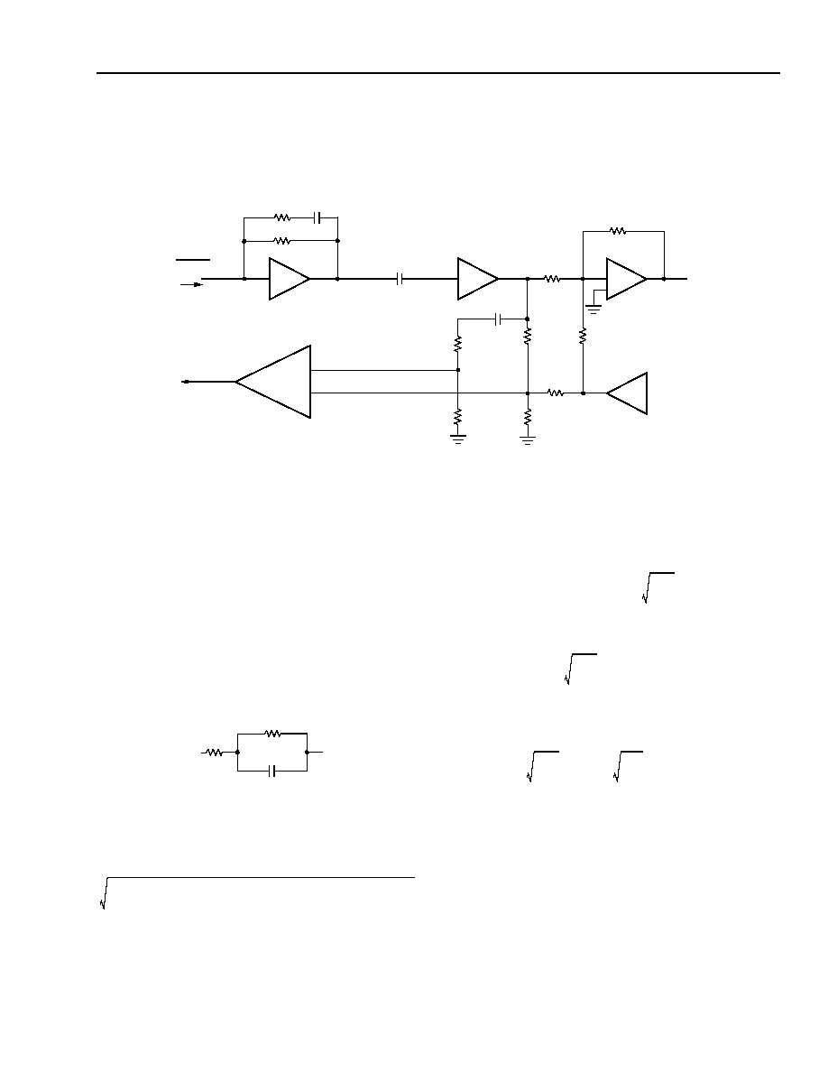
Preliminary Data Sheet
October 2001
Low-Cost Ringing SLIC
L9214A/G
Agere Systems Inc.
35
ac Applications
(continued)
Design Examples
(continued)
ac Interface Using First-Generation Codec (continued)
5-6400.H (F)
Figure 15. Interface Circuit Using First-Generation Codec (Blocking Capacitors Not Shown)
0.1
µ
F
R
TGS
V
TX
R
GX
= 4750
T
XI
V
ITR
R
T6
R
x
R
T3
R
HB
CODEC
OUTPUT
DRIVE
AMP
CODEC
OP AMP
≠
+
20
C
N
R
N1
R
N2
R
GP
R
RCV
≠I
T/R
318.25
C
GS
RCVN
RCVP
Transmit Gain
Transmit gain will be specified as a gain from T/R to
PCM, T
X
(dB). Since PCM is referenced to 600
and
assumed to be 0 dB, and in the case of T/R being refer-
enced to some complex impedance other than 600
resistive, the effects of the impedance transformation
must be taken into account.
Again, specified complex termination impedance at T/R
is of the form:
5-6396(F)
First, calculate the equivalent resistance of this network
at the midband frequency of 1000 Hz.
R
EQ
=
Using R
EQ
, calculate the desired transmit gain, taking
into account the impedance transformation:
T
X
(dB) = T
X (specified[dB])
+ 20log
T
X (specified[dB])
is the specified transmit gain. 600
is the
impedance at the PCM, and R
EQ
is the impedance at
Tip and ring. 20log
represents the power
loss/gain due to the impedance transformation.
Note in the case of a 600
pure resistive termination
at T/R 20log
= 20log
= 0.
Thus, there is no power loss/gain due to impedance
transformation and T
X
(dB) = T
X (specified[dB])
.
Finally, convert T
X
(dB) to a ratio, g
tx
:
T
X
(dB) = 20log g
tx
The ratio of R
X
/R
T6
is used to set the transmit gain:
= g
tx
∑
∑
with a quad Agere codec
such as T7504:
R
X
< 200 k
R
2
C
R
1
2
f
(
)
2
C
12
R
1
R
22
R
1
R
2
+
+
1
2
f
(
)
2
R
22
C
12
+
-----------------------------------------------------------------------------
2
2
f
R
22
C
12
1
2
f
(
)
2
R
22
C
12
+
---------------------------------------------------
2
+
600
R
EQ
-----------
600
R
EQ
-----------
600
R
EQ
-----------
600
600
----------
R
X
R
T6
----------
318.25
20
------------------
1
M
-----

Preliminary Data Sheet
October 2001
Low-Cost Ringing SLIC
L9214A/G
36
Agere Systems Inc.
ac Applications
(continued)
Design Examples
(continued)
ac Interface Using First-Generation Codec (contin-
ued)
Receive Gain
Ratios of R
RCV
, R
T3
, R
GP
will set both the low-frequency
termination and receive gain for the complex case. In
the complex case, additional high-frequency compen-
sation, via C
N
, R
N1
, and R
N2
, is needed for the return
loss characteristic. For resistive termination, C
N
, R
N1
,
and R
N2
are not used and RCVN is tied to ground via a
resistor.
Determine the receive gain, g
rcv
, taking into account the
impedance transformation in a manner similar to trans-
mit gain.
R
X
(dB) = R
X (specified[dB])
+ 20log
R
X
(dB) = 20log g
rcv
Then:
g
rcv
=
and low-frequency termination
Z
TER(low)
=
+ 2R
P
+ 36
Z
TER(low)
is the specified termination impedance assum-
ing low frequency (C or C¥ is open).
R
P
is the series protection resistor.
36
is the typical internal feed resistance.
These two equations are best solved using a computer
spreadsheet.
Next, solve for the high-frequency return loss compen-
sation circuit, C
N
, R
N1
, and R
N2
:
C
N
R
N2
=
C
G
R
TGP
R
N1
= R
N2
There is an input offset voltage associated with nodes
RCVN and RCVP. To minimize the effect of mismatch
of this voltage at T/R, the equivalent resistance to ac
ground at RCVN should be approximately equal to that
at RCVP. Refer to Figure 16 (with dc blocking capaci-
tors). To meet this requirement, R
N2
= R
GP
|| R
T3
.
Hybrid Balance
Set the hybrid cancellation via R
HB
.
R
HB
=
If a 5 V only codec such as the Agere T7504 is used,
dc blocking capacitors must be added as shown in Fig-
ure 16. This is because the codec is referenced to
2.5 V and the SLIC to ground--with the ac coupling, a
dc bias at T/R is eliminated and power associated with
this bias is not consumed.
Typically, values of 0.1 µF to 0.47 µF capacitors are
used for dc blocking. The addition of blocking capaci-
tors will cause a shift in the return loss and hybrid bal-
ance frequency response toward higher frequencies,
degrading the lower-frequency response. The lower
the value of the blocking capacitor, the more pro-
nounced the effect is, but the cost of the capacitor is
lower. It may be necessary to scale resistor values
higher to compensate for the low-frequency response.
This effect is best evaluated via simulation. A PSPICE
Æ
model for the L9214 is available.
Design equation calculations seldom yield standard
component values. Conversion from the calculated
value to standard value may have an effect on the ac
parameters. This effect should be evaluated and opti-
mized via simulation.
R
EQ
600
-----------
4
1
R
RCV
R
T3
---------------
R
RCV
R
GP
---------------
+
+
------------------------------------------------
2400
1
R
T3
R
GP
------------
R
T3
R
RCV
---------------
+
+
--------------------------------------------
2R
P
2400
-------------
2400
2R
P
-------------
R
T GS
R
T GP
--------------
1
≠
R
X
g
rc v
g
tx
◊
-------------------------
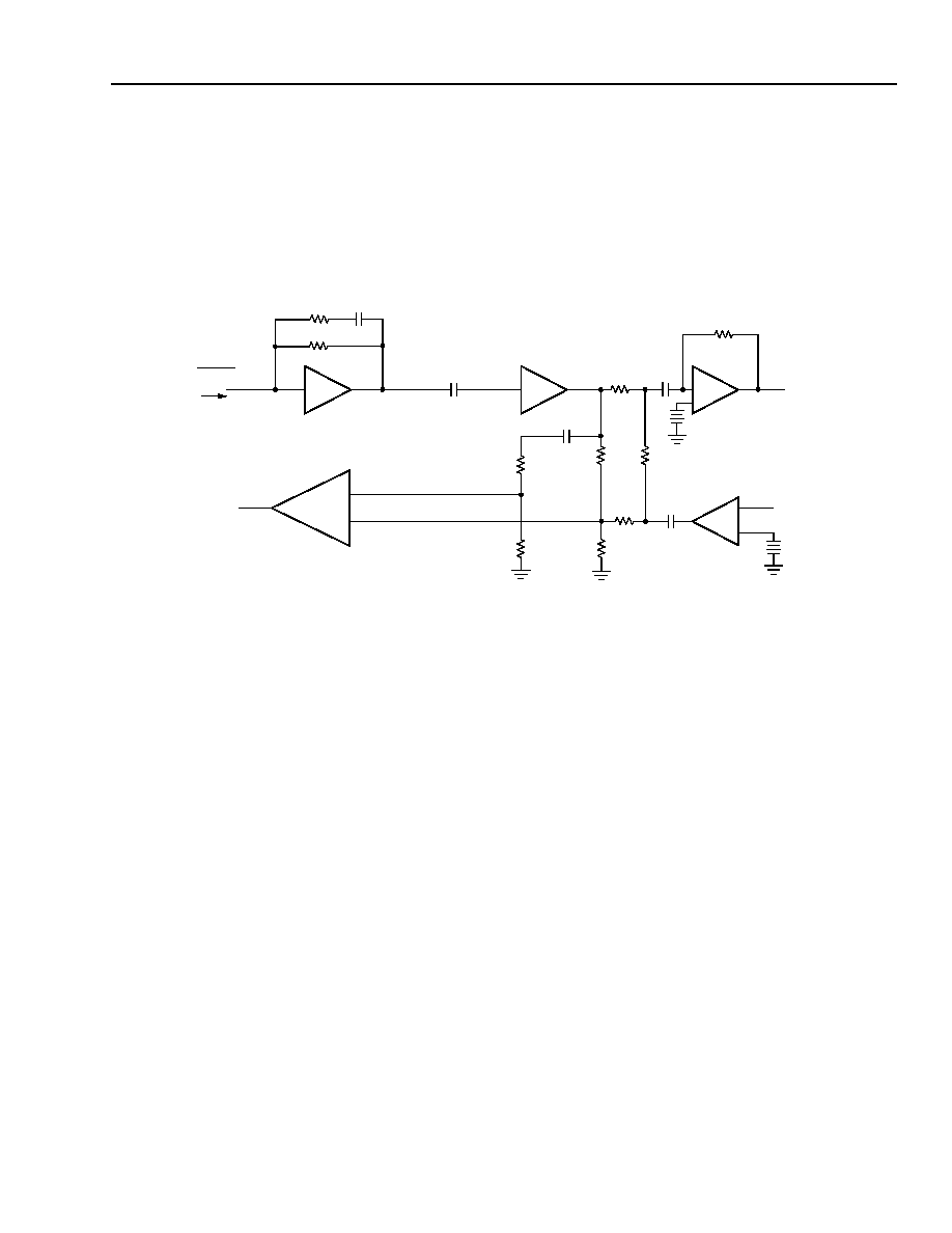
Preliminary Data Sheet
October 2001
Low-Cost Ringing SLIC
L9214A/G
Agere Systems Inc.
37
ac Applications
(continued)
Design Examples
(continued)
ac Interface Using First-Generation Codec (continued)
Blocking Capacitors
5-6401.G (F)
Figure 16. ac Interface Using First-Generation Codec (Including Blocking Capacitors) for Complex
Termination Impedance
0.1
µ
F
R
TGS
VTX
R
GX
= 4750
TXI
VITR
R
T6
R
x
R
T3
R
HB
CODEC
OUTPUT
DRIVE
AMP
CODEC
OP AMP
≠
+
20
C
N
R
N1
R
N2
R
GP
R
RCV
RCVN
RCVP
≠I
T/R
318.25
C
GS
C
B1
2.5 V
C
B2
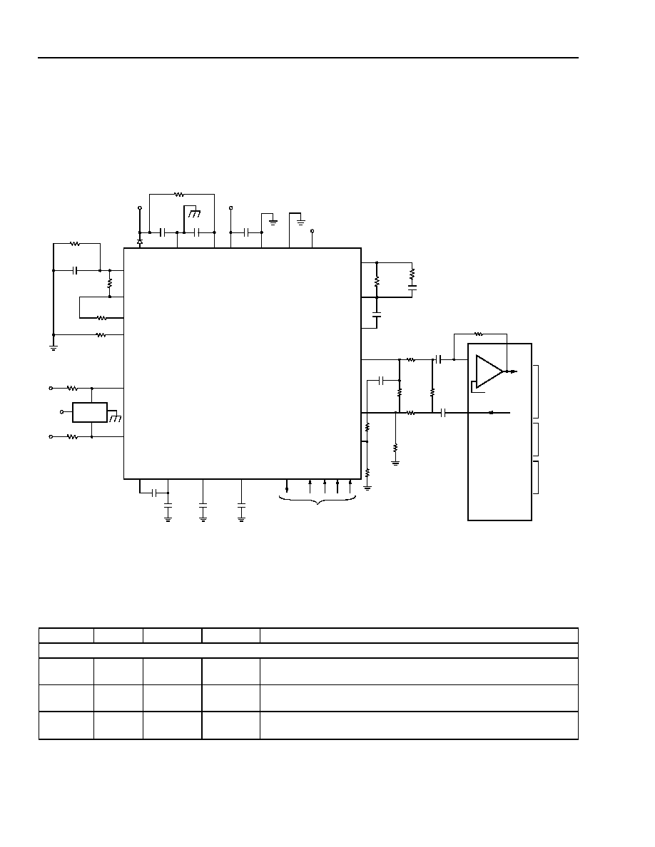
Preliminary Data Sheet
October 2001
Low-Cost Ringing SLIC
L9214A/G
38
Agere Systems Inc.
ac Applications
(continued)
Design Examples
(continued)
ac Interface Using First-Generation Codec (continued)
12-3535.m (F)
Figure 17. Agere T7504 First-Generation Codec; Complex Termination with Power Control Resistor (3 REN
Configuration)
Table 21. L9214 Parts List for Agere T7504 First-Generation Codec; Complex Termination with Power
Control Resistor
Name
Value
Tolerance
Rating
Function
Fault Protection
R
PT
30
1%
Fusible or
PTC
Protection resistor.
R
PR
30
1%
Fusible or
PTC
Protection resistor.
Protector
Agere
L7591
--
--
Secondary protection.
V
BAT1
BGND
V
BAT2
V
CC
AGND
ICM TRGDET
ground key
not used
C
VBAT1
0.1
µ
F
C
VBAT2
0.1
µ
F
C
CC
0.1
µ
F
PR
PT
AGERE
L7591
V
BAT1
FUSIBLE RESISTOR
30
VITR
RCVP
RCVN
ITR
VTX
TXI
R
GX
4750
R
TGS
C
GS
V
BAT1
V
CC
C
TX
0.1
µ
F
1/4 T7504
CODEC
R
T6
GSX
+2.4 V
R
HB1
R
T3
R
RCV
C
N
R
GP
DX
DR
FSE
FSEP
MCLK
ASEL
CONTROL
INPUTS
SYNC
AND
PCM
HIGHWAY
CLOCK
R
N2
≠
+
30
C
C2
L9214A
C
C1
CF1
CF2
FB1
FB2
NSTAT B3 B2 B1 B0
C
F1
0.22
µ
F
C
F2
0.1
µ
F
FROM/TO CONTROL
FUSIBLE RESISTOR
47.5 k
54.9 k
127 k
R
N1
49.9 k
113 k
120 pF
0.1
µ
F
0.1
µ
F
40.6 k
C
FB1
0.01
µ
F
C
FB2
0.01
µ
F
OR PTC
OR PTC
RTFLT
DCOUT
I
PROG
(I
LOOP
= 25 mA)
I
REF
R
RT2
R
RT1
133 k
C
RT
1
µ
F
75 k
R
IPROG
5.76 k
R
IREF
28.7 k
VF
X
IN
R
X
115
k
VF
R
O
1.74
k
12 nF
R
PWR
2.0 k
59.0 k
D
BAT1

Preliminary Data Sheet
October 2001
Low-Cost Ringing SLIC
L9214A/G
Agere Systems Inc.
39
Applications
(continued)
Design Examples
(continued)
ac Interface Using First-Generation Codec (continued)
Table 21. L9214 Parts List for Agere T7504 First-Generation Codec; Complex Termination with Power Con-
trol Resistor (continued)
Note: T
X
= 0 dBm, R
X
= 0 dBm, termination impedance = 220
+ (820
|| 115 nF)
,
hybrid balance = 220
+ (820
|| 115 nF)
.
Name
Value
Tolerance
Rating
Function
Power Supply
C
VBAT1
0.1
µ
F
20%
100 V
V
BAT
filter capacitor.
C
VBAT2
0.1
µ
F
20%
50 V
V
BAT
filter capacitor. |V
BAT2
| < |V
BAT1
|.
D
BAT1
1N4004
--
--
Reverse current.
C
CC
0.1
µ
F
20%
10 V
V
CC
filter capacitor.
C
F1
0.22
µ
F
20%
100 V
Filter capacitor.
C
F2
0.1
µ
F
20%
100 V
Filter capacitor.
R
PWR
2.0 k
5%
2 W
Power control resistor, provides single battery supply operation.
dc Profile
R
IPROG
5.76 k
1%
1/16 W
With R
IREF
,
fixes dc current limit.
R
IREF
28.7 k
1%
1/16 W
With R
IPROG
,
fixes dc current limit.
Ringing/Ring Trip
C
RING
1.0
µ
F
20%
10 V
Ring trip filter capacitor.
R
RT1
133 k
1%
1/16 W
Ring trip filter resistor.
R
RT2
75 k
1%
1/16 W
Ring trip filter resistor.
C
FB1
0.01
µ
F
20%
100 V
With C
FB2
, slows rate of battery reversal. Sets crest factor of bal-
anced power ring signal.
C
FB2
0.01
µ
F
20%
100 V
With C
FB1
, slows rate of battery reversal. Sets crest factor of bal-
anced power ring signal.
ac Interface
R
GX
4750
1%
1/16 W
Sets T/R to VITR transconductance.
R
TGS
1.74 k
1%
1/16 W
Gain shaping for complex termination.
C
GS
12 nF
5%
10 V
Gain shaping for complex termination.
C
TX
0.1
µ
F
20%
10 V
ac/dc separation.
C
C1
0.1
µ
F
20%
10 V
dc blocking capacitor.
C
C2
0.1
µ
F
20%
10 V
dc blocking capacitor.
R
T3
49.9 k
1%
1/16 W
With R
GP
and R
RCV
, sets termination impedance and receive gain.
R
T6
40.2 k
1%
1/16 W
With R
X
, sets transmit gain.
R
X
115 k
1%
1/16 W
With R
T6
, sets transmit gain.
R
HB1
113 k
1%
1/16 W
With R
X
, sets hybrid balance.
R
RCV
59.0 k
1%
1/16 W
With R
GP
and R
T3
, sets termination impedance and receive gain.
R
GP
54.9 k
1%
1/16 W
With R
RCV
and R
T3
, sets termination impedance and receive gain.
C
N
120 pF
20%
10 V
High frequency compensation.
R
N1
127 k
1%
1/16 W
High frequency compensation.
R
N2
47.5 k
1%
1/16 W
High frequency compensation, compensate for dc offset at
RCVP/RCVN.
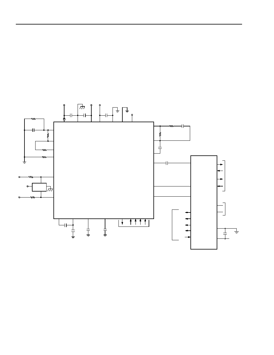
Preliminary Data Sheet
October 2001
Low-Cost Ringing SLIC
L9214A/G
40
Agere Systems Inc.
ac Applications
(continued)
Design Examples
(continued)
Third-Generation Codec ac Interface Network--Complex Termination
The following reference circuit shows the complete SLIC schematic for interface to the Agere T8536 third-genera-
tion codec. All ac parameters are programmed by the T8536. Note this codec differentiates itself in that no external
components are required in the ac interface to provide a dc termination impedance or for stability. Please see the
T8535/6 data sheet for information on coefficient programming.
12-3534.Z1 (F)
Figure 18. Third-Generation Codec ac Interface Network; Complex Termination (3 REN Configuration)
V
BAT1
BGND
V
BAT2
V
CC
AGND ICM TRGDET
ground key
not used
C
VBAT1
0.1
µ
F
C
VBAT2
0.1
µ
F
C
CC
0.1
µ
F
PR
PT
AGERE
L7591
V
BAT1
50
50
CF1
CF2
FB1
FB2
NSTAT B3 B2 B1 B0
C
F1
0.22
µ
F
C
F2
0.1
µ
F
VITR
RCVP
RCVN
ITR
VTX
TXI
R
GX
4750
V
BAT1
V
BAT2
V
CC
C
TX
0.1
µ
F
C
C1
PCM
HIGHWAY
DX0
DR0
DX1
DR1
FS
BCLK
DGND
V
DD
SYNC
AND
V
DD
VF
X
I
VF
R
OP
VF
R
ON
SLIC5a
SLIC4a
SLIC3a
SLIC2a
SLIC0a
CLOCK
L9214G
FROM/TO
CONTROL
B3
B2
B0
NSTAT
B1
0.1
µ
F
FUSIBLE RESISTOR
OR PTC
OR PTC
FUSIBLE RESISTOR
RTFLT
DCOUT
I
PROG
(I
LOOP
= 25 mA)
I
REF
R
RT2
R
RT1
133 k
C
RT
1
µ
F
75 k
R
IPROG
5.76 k
R
IREF
28.7 k
C
FB1
0.01
µ
F
C
FB2
0.01
µ
F
R
CR
C
CC1
D
BAT1
820 pF
2 k
1/4 T8536
CODEC

Preliminary Data Sheet
October 2001
Low-Cost Ringing SLIC
L9214A/G
Agere Systems Inc.
41
ac Applications
(continued)
Design Examples
(continued)
Third-Generation Codec ac Interface Network--Complex Termination (continued)
Table 22. L9214 Parts List for Agere T8536 Third-Generation Codec Meter Pulse Application ac and dc
Parameters; Fully Programmable
* For loop stability, increase to 50
minimum if synthesizing 900
or 900
+ 2.16
µ
F termination impedance.
Name
Value
Tolerance
Rating
Function
Fault Protection
R
PT
30
1%
Fusible or PTC Protection resistor*.
R
PR
30
1%
Fusible or PTC Protection resistor*.
Protector
Agere L7591
--
--
Secondary protection.
Power Supply
C
VBAT1
0.1
µ
F
20%
100 V
V
BAT
filter capacitor.
C
VBAT2
0.1
µ
F
20%
50 V
V
BAT
filter capacitor. |V
BAT2
| < |V
BAT1
|.
D
BAT1
1N4004
--
--
Reverse current.
C
CC
0.1
µ
F
20%
10 V
V
CC
filter capacitor.
C
F1
0.22
µ
F
20%
100 V
Filter capacitor.
C
F2
0.1
µ
F
20%
100 V
Filter capacitor.
dc Profile
R
IPROG
5.76 k
1%
1/16 W
With R
IREF
, fixes dc current limit.
R
IREF
28.7 k
1%
1/16 W
With R
IPROG
, fixes dc current limit.
Ringing/Ring Trip
C
RT
1.0
µ
F
20%
10 V
Ring trip filter capacitor.
R
RT1
133 k
1%
1/16 W
Ring trip filter resistor.
R
RT2
75 k
1%
1/16 W
Ring trip filter resistor.
C
FB1
0.01
µ
F
20%
100 V
With C
FB2
, slows rate of battery reversal. Sets crest fac-
tor of balanced power ring signal.
C
FB2
0.01
µ
F
20%
100 V
With C
FB1
, slows rate of battery reversal. Sets crest fac-
tor of balanced power ring signal.
ac Interface
R
GX
4750
1%
1/16 W
Sets T/R to VITR transconductance.
R
CR
10 k
5%
1/16 W
Compensation resistor.
C
CC1
270 pF
20%
10 V
Compensation capacitor.
C
TX
0.1
µ
F
20%
10 V
ac/dc separation.
C
C1
0.1
µ
F
20%
10 V
dc blocking capacitor.

Preliminary Data Sheet
October 2001
Low-Cost Ringing SLIC
L9214A/G
42
Agere Systems Inc.
Outline Diagrams
28-Pin SOG
Note: The dimensions in these outline diagrams are intended for informational purposes only. For detailed draw-
ings to assist your design efforts, please contact your Agere Sales Representative.
5-4414
Package Dimensions
Package
Description
Number
of Pins
N
Maximum
Length
L
Maximum Width
Without Leads
B
Maximum Width
Including Leads
W
Maximum Height
Above Board
H
SOG (small outline gull-wing)
28
18.11
7.62
10.64
2.67
W
0.61
0.51 MAX
H
0.28 MAX
0.10
SEATING PLANE
1.27 TYP
N
L
B
1
PIN #1 IDENTIFIER ZONE
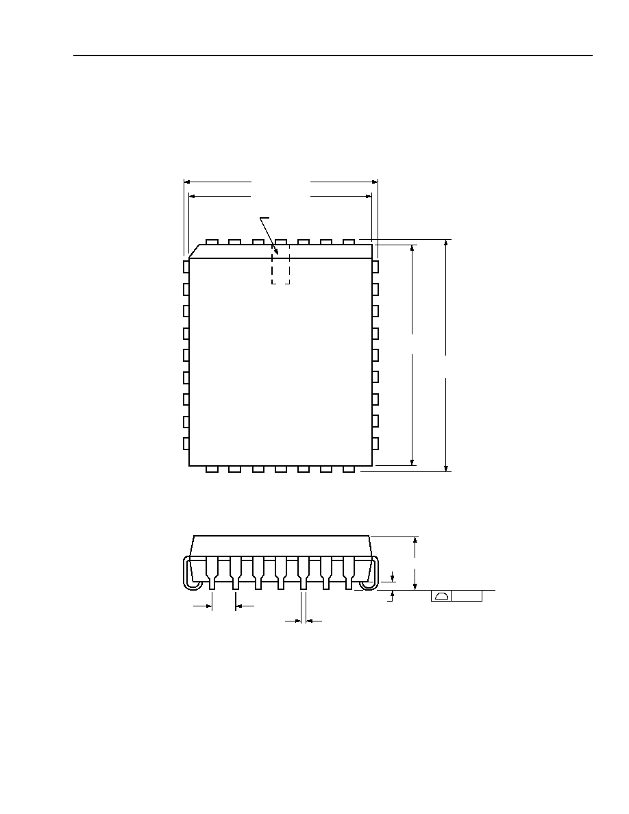
Preliminary Data Sheet
October 2001
Low-Cost Ringing SLIC
L9214A/G
Agere Systems Inc.
43
Outline Diagrams
(continued)
32-Pin PLCC
Note: The dimensions in this outline diagram are intended for informational purposes only. For detailed schemat-
ics to assist your design efforts, please contact your Agere Sales Representative.
5-3813r2 (F)
0.10
SEATING PLANE
0.38 MIN
TYP
1.27 TYP
0.330/0.533
1
4
30
5
13
21
29
14
20
12.446
±
0.127
11.430
±
0.076
PIN #1 IDENTIFIER
ZONE
14.986
±
0.127
13.970
±
0.076
3.175/3.556
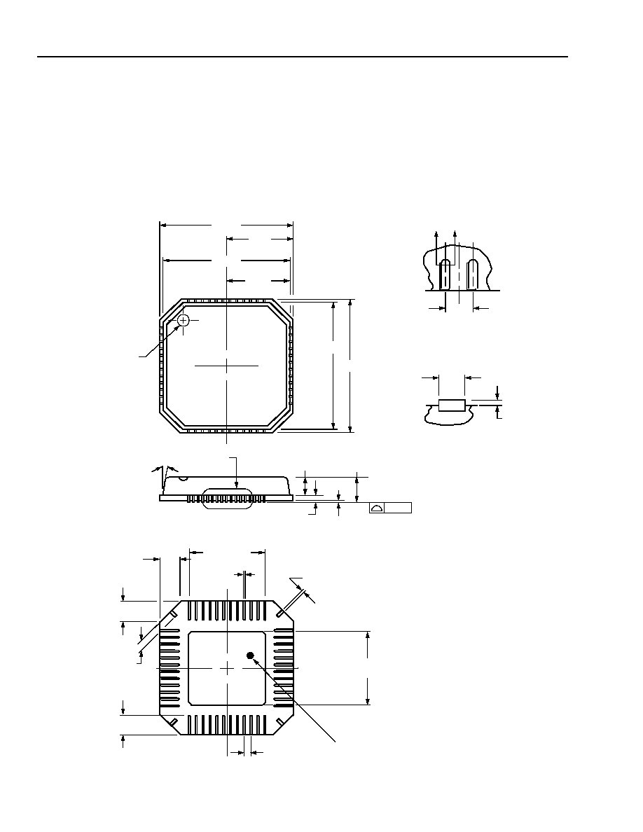
Preliminary Data Sheet
October 2001
Low-Cost Ringing SLIC
L9214A/G
44
Agere Systems Inc.
Outline Diagrams
(continued)
48-Pin MLCC
Dimensions are in millimeters.
Notes: The dimensions in this outline diagram are intended for informational purposes only. For detailed schemat-
ics to assist your design efforts, please contact your Agere Sales Representative.
The exposed pad on the bottom of the package will be at V
BAT1
potential.
0195
PIN #1
IDENTIFIER ZONE
1
7.00
6.75
SEATING PLANE
0.08
0.65/0.80
0.20 REF
DETAIL A
7.00
5.10
± 0.15
3
3.50
3.375
6.75
0.00/0.05
SECTION C≠C
11 SPACES @
0.50 = 5.50
0.50 BSC
0.13/0.23
0.18/0.30
0.30/0.45
0.01/0.05
1.00 MAX
12∞
0.18/0.30
0.24/0.60
0.24/0.60
2
1
3
2
0.20/0.45
0.50 BSC
DETAIL A
C
C
VIEW FOR EVEN TERMINAL/SIDE
C
L
EXPOSED PAD
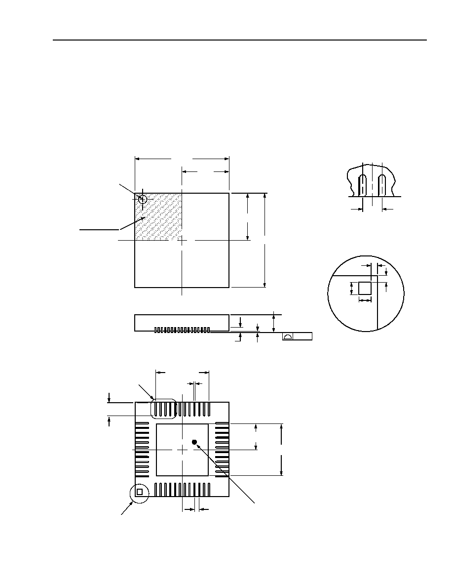
Preliminary Data Sheet
October 2001
Low-Cost Ringing SLIC
L9214A/G
Agere Systems Inc.
45
Outline Diagrams
(continued)
48-Pin MLCC, JEDEC MO-220 VKKD-2
Dimensions are in millimeters.
Notes: The dimensions in this outline diagram are intended for informational purposes only. For detailed schemat-
ics to assist your design efforts, please contact your Agere Sales Representative.
The exposed pad on the bottom of the package will be at V
BAT1
potential.
0195
INDEX AREA
7.00
3.50
SEATING PLANE
0.08
0.20 REF
DETAIL A
7.00
5.00/5.25
3.50
11 SPACES @
0.50 = 5.50
0.50 BSC
0.18/0.30
0.02/0.05
1.00 MAX
0.23
0.30/0.50
1
3
2
(7.00/2 x 7.00/2)
PIN #1
IDENTIFIER ZONE
TOP VIEW
SIDE VIEW
DETAIL B
0.23
0.18
0.18
BOTTOM VIEW
2.50/2.625
EXPOSED PAD
DETAIL B
0.50 BSC
DETAIL A
VIEW FOR EVEN TERMINAL/SIDE
C
L

Preliminary Data Sheet
October 2001
Low-Cost Ringing SLIC
L9214A/G
Agere Systems Inc. reserves the right to make changes to the product(s) or information contained herein without notice. No liability is assumed as a result of their use or application.
Copyright © 2001 Agere Systems Inc.
All Rights Reserved
October 2001
DS01-144ALC (Replaces DS00-342ALC)
For additional information, contact your Agere Systems Account Manager or the following:
INTERNET:
http://www.agere.com
E-MAIL:
docmaster@agere.com
N. AMERICA:
Agere Systems Inc., 555 Union Boulevard, Room 30L-15P-BA, Allentown, PA 18109-3286
1-800-372-2447, FAX 610-712-4106 (In CANADA: 1-800-553-2448, FAX 610-712-4106)
ASIA:
Agere Systems Hong Kong Ltd., Suites 3201 & 3210-12, 32/F, Tower 2, The Gateway, Harbour City, Kowloon
Tel. (852) 3129-2000, FAX (852) 3129-2020
CHINA: (86) 21-5047-1212 (Shanghai), (86) 10-6522-5566 (Beijing), (86) 755-695-7224 (Shenzhen)
JAPAN: (81) 3-5421-1600 (Tokyo), KOREA: (82) 2-767-1850 (Seoul), SINGAPORE: (65) 778-8833, TAIWAN: (886) 2-2725-5858 (Taipei)
EUROPE:
Tel. (44) 7000 624624, FAX (44) 1344 488 045
Ordering Information
* Please contact your Agere Sales Representative for availability.
UL is a trademark of Underwriters Laboratories, Inc.
IEC is a registered trademark of the International Electrotechnical Commission.
IEEE is a registered trademark of The Institute of Electrical and Electronics Engineers, Inc.
PSPICE is a registered trademark of MicroSim Corporation.
Telcordia Technologies is a trademark of Bell Communications Research, Inc.
Device Part No.
Description
Package
Comcode
LUCL9214AAJ-D
SLIC Gain = 8
28-Pin SOG*, Dry-bagged
108553892
LUCL9214AAJ-DT
SLIC Gain = 8
28-Pin SOG*, Dry-bagged, Tape and Reel
108553900
LUCL9214AAU-D
SLIC Gain = 8
32-Pin PLCC, Dry-bagged
108697905
LUCL9214AAU-DT
SLIC Gain = 8
32-Pin PLCC, Dry-bagged, Tape and Reel
108697913
LUCL9214ARG-D
SLIC Gain = 8
48-Pin MLCC, Dry-bagged
109058636
LUCL9214ARG-DT
SLIC Gain = 8
48-Pin MLCC, Dry-bagged, Tape and Reel
109058644
LUCL9214GAJ-D
SLIC Gain = 2
28-Pin SOG*, Dry-bagged
108560723
LUCL9214GAJ-DT
SLIC Gain = 2
28-Pin SOG*, Dry-bagged, Tape and Reel
108560731
LUCL9214GAU-D
SLIC Gain = 2
32-Pin PLCC, Dry-bagged
108698309
LUCL9214GAU-DT
SLIC Gain = 2
32-Pin PLCC, Dry-bagged, Tape and Reel
108698317
LUCL9214GRG-D
SLIC Gain = 2
48-Pin MLCC, Dry-bagged
109058651
LUCL9214GRG-DT
SLIC Gain = 2
48-Pin MLCC, Dry-bagged, Tape and Reel
109058669