
Data Sheet
September 2001
L9215A/G
Short-Loop Sine Wave Ringing SLIC
Introduction
The Agere Systems Inc. L9215 is a subscriber line
interface circuit that is optimized for short-loop,
power-sensitive applications. This device provides
the complete set of line interface functionality (includ-
ing power ringing) needed to interface to a subscriber
loop. This device has the capability to operate with a
V
CC
supply of 3.3 V or 5 V and is designed to mini-
mize external components required at all device
interfaces.
Features
s
Onboard ringing generation
s
Three ringing input options:
-- Sine wave
-- PWM
-- Logic level square wave
s
Flexible V
CC
options:
-- 5 V or 3.3 V V
CC
-- No �5 V required
s
Battery switch to minimize off-hook power
s
11 operating states:
-- Scan mode for minimal power dissipation
-- Forward and reverse battery active
-- On-hook transmission states
-- Meter pulse states
-- Ring mode
-- Disconnect mode
s
Ultralow on-hook power:
-- 27 mW scan mode
-- 42 mW active mode
s
Two SLIC gain options to minimal external compo-
nents in codec interface
s
Loop start, ring trip, and ground key detectors
s
Software- or hardware-controllable current-limit
and overhead voltage
s
Meter pulse compatible
s
32-pin PLCC package
s
48-pin MLCC package
Applications
s
Voice over Internet Protocol (VoIP)
s
Cable Modems
s
Terminal Adapters (TA)
s
Wireless Local Loop (WLL)
s
Telcordia
Technologies
TM
GR-909 Access
s
Network Termination (NT)
s
Key Systems
Description
This device is optimized to provide battery feed, ring-
ing, and supervision on short-loop plain old tele-
phone service (POTS) loops.
This device provides power ring to the subscriber
loop through amplification of a low-voltage input. It
provides forward and reverse battery feed states, on-
hook transmission, a low-power scan state, meter
pulse states, and a forward disconnect state.
The device requires a V
CC
and battery to operate.
V
CC
may be either a 5 V or a 3.3 V supply. The ring-
ing signal is derived from the high-voltage battery. A
battery switch is included to allow for use of a lower-
voltage battery in the off-hook mode, thus minimizing
short-loop off-hook power.
Loop closure, ring trip, and ground key detectors are
available. The loop closure detector has a fixed
threshold with hysteresis. The ring trip detector
requires a single-pole filter, thus minimizing external
components required.
This device supports meter pulse applications. Meter
pulse is injected into a dedicated meter pulse input.
Injection of meter pulse onto tip and ring is controlled
by the device's logic input pin.
Both the dc current limit and overhead voltage are
programmable. Programming may be done by exter-
nal resistors or an applied voltage source. If the volt-
age source is programmable, the current limit and
overhead may be set via software control.
The device is offered with two gain options. This
allows for an optimized codec interface, with minimal
external components regardless of whether a first-
generation or a programmable third-generation
codec is used.

Data Sheet
September 2001
Short-Loop Sine Wave Ringing SLIC
L9215A/G
2
Agere Systems Inc.
Table of Contents
Contents
Page
Introduction..................................................................1
Features ....................................................................1
Applications...............................................................1
Description ................................................................1
Features ......................................................................4
Description...................................................................4
Architecture Diagram...................................................7
Pin Information ............................................................8
Operating States........................................................11
State Definitions ........................................................12
Forward Active ........................................................12
Reverse Active ........................................................12
Forward Active with PPM ........................................12
Reverse Active with PPM........................................12
Scan ........................................................................12
On-Hook Transmission--Forward Battery ..............12
On-Hook Transmission with PPM--Forward
Battery ....................................................................13
On-Hook Transmission--Reverse Battery ..............13
On-Hook Transmission with PPM--Reverse
Battery ....................................................................13
Disconnect ..............................................................13
Ring.........................................................................13
Thermal Shutdown ..................................................13
Absolute Maximum Ratings.......................................14
Electrical Characteristics ...........................................15
Test Configurations ...................................................22
Applications ...............................................................24
Power Control .........................................................24
dc Loop Current Limit..............................................24
Overhead Voltage ...................................................25
Active Mode .........................................................25
On-Hook Transmission Mode...............................26
Scan Mode ...........................................................26
Ring Mode ............................................................26
Contents
Page
Loop Range ........................................................... 26
Battery Reversal Rate ............................................ 26
Supervision............................................................... 27
Loop Closure.......................................................... 27
Ring Trip ................................................................ 27
Tip or Ring Ground Detector .................................. 27
Power Ring ............................................................ 27
Sine Wave Input Signal and Sine Wave Power
Ring Signal Output............................................ 28
PWM Input Signal and Sine Wave Power
Ring Signal Output............................................ 30
5 V V
CC
Operation ............................................... 31
3.3 V V
CC
Operation ............................................ 32
Square Wave Input Signal and Trapezoidal
Power Ring Signal Output ................................ 32
Periodic Pulse Metering (PPM) ................................ 34
ac Applications ......................................................... 34
ac Parameters........................................................ 34
Codec Types .......................................................... 34
First-Generation Codecs ..................................... 34
Third-Generation Codecs .................................... 34
ac Interface Network .............................................. 34
Design Examples ................................................... 35
First-Generation Codec ac Interface
Network--Resistive Termination ...................... 35
Example 1, Real Termination .............................. 36
First-Generation Codec ac Interface
Network--Complex Termination ....................... 39
Complex Termination Impedance Design
Example ............................................................ 39
ac Interface Using First-Generation Codec ......... 39
Set Z
TG
--Gain Shaping ....................................... 39
Transmit Gain...................................................... 40
Receive Gain....................................................... 41
Hybrid Balance .................................................... 41
Blocking Capacitors............................................. 42
Third-Generation Codec ac Interface
Network--Complex Termination ....................... 45
Outline Diagrams...................................................... 47
32-Pin PLCC .......................................................... 47
48-Pin
MLCC.......................................................... 48
48-Pin
MLCC, JEDEC MO-220 VKKD-2................ 49
Ordering Information................................................. 50

Data Sheet
September 2001
Short-Loop Sine Wave Ringing SLIC
L9215A/G
Agere Systems Inc.
3
Table of Contents
(continued)
Figures
Page
Figure 1. Architecture Diagram ...................................7
Figure 2. 32-Pin PLCC Diagram .................................8
Figure 3. 48-Pin MLCC Diagram .................................8
Figure 4. Basic Test Circuit ......................................22
Figure 5. Metallic PSRR ...........................................23
Figure 6. Longitudinal PSRR ....................................23
Figure 7. Longitudinal Balance .................................23
Figure 8. ac Gains ....................................................23
Figure 9. Ringing Waveform Crest Factor = 1.6 .......27
Figure 10. Ringing Waveform Crest Factor = 1.2 .....27
Figure 11. Ring Mode Typical Operation ...................28
Figure 12. RING
IN
Operation ....................................29
Figure 13. L9215/16 Ringing Input Circuit Selection
Table for Square Wave and PWM
Inputs........................................................30
Figure 14. Modulation Waveforms ............................31
Figure 15. 5 V PWM Signal Amplitude ......................31
Figure 16. Ringing Output on RING, with
Vcc = 5 V..................................................31
Figure 17. 3.3 V PWM Signal Amplitude ...................32
Figure 18. Ringing Output on RING, with
Vcc = 3.1 V...............................................32
Figure 19. Square Wave Input Signal and Trapezoidal
Power Ring Signal Output ........................32
Figure 20. Crest Factor vs. Battery Voltage...............33
Figure 21. Crest Factor vs. R (k
) ............................33
Figure 22. ac Equivalent Circuit ................................36
Figure 23. Agere T7504 First-Generation Codec
Resistive Termination; Nonmeter Pulse
Application................................................37
Figure 24. Interface Circuit Using First-Generation
Codec (Blocking Capacitors
Not Shown) ..............................................40
Figure 25. ac Interface Using First-Generation
Codec (Including Blocking Capacitors)
for Complex Termination Impedance ......42
Figure 26. Agere T7504 First-Generation Codec
Complex Termination; Meter Pulse
Application................................................43
Figure 27. Third-Generation Codec ac Interface
Network; Complex Termination ...............45
Tables
Page
Table 1. Pin Descriptions ........................................... 9
Table 2. Control States ............................................ 11
Table 3. Supervision Coding .................................... 11
Table 4. Recommended Operating
Characteristics ........................................... 14
Table 5. Thermal Characteristics.............................. 14
Table 6. Environmental Characteristics .................... 15
Table 7. 5 V Supply Currents ................................... 15
Table 8. 5 V Powering .............................................. 15
Table 9. 3.3 V Supply Currents................................. 16
Table 10. 3.3 V Powering ......................................... 16
Table 11. 2-Wire Port .............................................. 17
Table 12. Analog Pin Characteristics ...................... 18
Table 13. ac Feed Characteristics ........................... 19
Table 14. Logic Inputs and Outputs (V
CC
= 5 V) ...... 20
Table 15. Logic Inputs and Outputs (V
CC
= 3.3 V) ... 20
Table 16. Ringing Specifications ............................. 21
Table 17. Ring Trip .................................................. 21
Table 18. PPM ......................................................... 21
Table 19. Typical Active Mode On- to Off-Hook
Tip/Ring Current-Limit Transient
Response ................................................ 25
Table 20. FB1 and FB2 Values vs. Typical
Ramp Time .............................................. 26
Table 21. Onset of Power Ringing Clipping
V
CC
= 5 V, Cinput = 0.47
�
F .................... 29
Table 22. Onset of Power Ringing Clipping
V
CC
= 3.1 V, Cinput = 0.47
�
F ................. 29
Table 23. Signal and Component Selection Chart ... 30
Table 24. Parts List L9215; Agere T7504
First-Generation Codec Resistive Termina-
tion; Nonmeter Pulse Application ............ 38
Table 25. Parts List L9215; Agere T7504
First-Generation Codec Complex Termina-
tion; Meter Pulse Application ................... 44
Table 26. Parts List L9215; Agere T8536
Third-Generation Codec Meter Pulse
Application ac and dc Parameters;
Fully Programmable ................................ 46

Data Sheet
September 2001
Short-Loop Sine Wave Ringing SLIC
L9215A/G
4
Agere Systems Inc.
Features
s
Onboard balanced ringing generation:
-- No ring relay
-- No bulk ring generator required
-- 15 Hz to 70 Hz ring frequency supported
-- Sine wave input-sine wave output
-- PWM input-sine wave output
-- Square wave input-trapezoidal output
s
Power supplies requirements:
-- V
CC
talk battery and ringing battery required
-- No �5 V supply required
-- No high-voltage positive supply required
s
Flexible Vcc options:
-- 5 V or 3.3 V V
CC
operation
-- 5 V or 3.3 V V
CC
interchangeable and transparent
to users
s
Logic-controlled battery switch:
-- Minimize off-hook power dissipation
s
Minimal external components required
s
11 operating states:
-- Forward active, V
BAT2
applied
-- Polarity reversal active, V
BAT2
applied
-- On-hook transmission, V
BAT1
applied
-- On-hook transmission polarity reversal, V
BAT1
applied
-- PPM active forward active, V
BAT2
applied
-- PPM active polarity reversal active, V
BAT2
applied
-- PPM active on-hook transmission, V
BAT1
applied
-- PPM active on-hook transmission polarity rever-
sal, V
BAT1
applied
-- Scan
-- Forward disconnect
-- Ring mode
s
Unlatched parallel data control interface
s
Ultralow SLIC power:
-- Scan 38 mW (V
CC
= 5 V)
-- Forward/reverse active 57 mW (V
CC
= 5 V)
-- Scan 27 mW (V
CC
= 3.3 V)
-- Forward/reverse active 42 mW (V
CC
= 3.3 V)
s
Supervision:
-- Loop start, fixed threshold with hysteresis
-- Ring trip, single-pole ring trip filtering, fixed thresh-
old as a function of battery voltage
-- Common-mode current for ground key applica-
tions, user-adjustable threshold
s
Adjustable current limit:
-- 10 mA to 70 mA programming range
s
Overhead voltage:
-- Clamped typically <51 V differentially
-- Clamped maximum <56.5 V single-ended
-- Adjustable in active mode
s
Thermal shutdown protection with hysteresis
s
Longitudinal balance:
-- ETSI/ITU-T balance
--
Telcordia
Technologies
GR-909 balance
s
Meter pulse compatible:
-- Dedicated meter pulse signal input
-- On-hook transmission of PPM
s
ac interface:
-- Two SLIC gain options to minimize external com-
ponents required for interface to first- or third-gen-
eration codecs
-- Sufficient dynamic range for direct coupling to
codec output
s
32-pin PLCC package/48-pin MLCC package
s
90 V CBIC-S technology
Description
The L9215 is designed to provide battery feed, ringing,
and supervision functions on short plain old telephone
service (POTS) loops. This device is designed for
ultralow power in all operating states.
The L9215 offers 11 operating states. The device
assumes use of a lower-voltage talk battery, a higher-
voltage ringing battery, and a V
CC
supply.
The L9215 requires only a positive V
CC
supply. No
�5 V supply is needed. The L9215 can operate with a
V
CC
of either 5 V or 3.3 V, allowing for greater user flex-
ibility. The choice of V
CC
voltage is transparent to the
user; the device will function with either supply voltage
connected.
Two batteries are used:
1. A high-voltage ring battery (V
BAT1
).
V
BAT1
is a maximum �75 V. V
BAT1
is used for power
ring signal amplification and for scan and on-hook
transmission modes. This supply is current limited
to approximately the maximum power ringing cur-
rent, typically 50 mA.
2. A lower-voltage talk battery (V
BAT2
).
V
BAT2
is used for active mode powering.

Data Sheet
September 2001
Short-Loop Sine Wave Ringing SLIC
L9215A/G
Agere Systems Inc.
5
Description
(continued)
Forward and reverse battery active modes are used for
off-hook conditions. Since this device is designed for
short-loop applications, the lower-voltage V
BAT2
is
applied during the forward and reverse active states
.
Battery reversal is quiet, without breaking the ac path.
Rate of battery reversal may be ramped to control
switching time.
The magnitude of the overhead voltage in the forward
and reverse active modes has a typical default value of
6.0 V, allowing for an undistorted signal of 3.14 dBm
into 900
. This overhead can be increased to accom-
modate higher signal levels and/or PPM. The ring trip
detector is turned off during active modes to conserve
power.
Because on-hook transmission is not allowed in the
scan mode, an on-hook transmission mode is defined.
This mode is functionally similar to the active mode,
except the tip ring voltage is derived from the higher
V
BAT1
rather than V
BAT2
.
In the on-hook transmission modes with a primary bat-
tery whose magnitude is greater than a nominal
51 V, the magnitude of the tip-to-ground and ring-to-
ground voltage is clamped at less than 56.5 V.
To minimize on-hook power, a low-power scan mode is
available. In this mode, all functions except off-hook
supervision are turned off to conserve power. On-hook
transmission is not allowed in the scan mode.
In the scan mode with a primary battery whose magni-
tude is greater than a nominal 51 V, the magnitude of
the tip-to-ground and ring-to-ground voltage is clamped
at less than 56.5 V.
A forward disconnect mode is provided, where all cir-
cuits are turned off and power is denied to the loop.
The device offers a ring mode, in which a power ring
signal is provided to the tip/ring pair. During the ring
mode, a user-supplied, low-voltage ring signal (ac cou-
pled) is input to the device's RING
IN
input. This signal is
amplified to produce the power ring signal. This signal
may be a sine wave or filtered square wave to produce
a sine wave on trapezoidal output. Ring trip detector
and common-mode current detector are active during
the ring mode.
This feature eliminates the need for a separate external
ring relay, associated external circuitry, and a bulk ring-
ing generator. See the Applications section of this data
sheet for more information.
PPM is injected at the PPM
IN
pin (ac coupled). This is a
high-impedance input that controls the PPM differential
voltage on tip and ring. The PPM signal may be
present at this pin at all times; however, PPM will only
be transmitted to tip and ring during a PPM active
mode. There are forward and reverse active, and for-
ward and reverse on-hook transmission modes with
PPM active.
No PPM shaping is done by the device. It is assumed
that a shaped PPM input is presented to PPM
IN
.
The maximum allowed PPM current at the 200
ac
meter pulse load to avoid saturation of the device's
internal AAC amplifier is 3 mArms. This signal level
is sufficient to provide a minimum 200 mVrms to the
200
PPM load under maximum specified dc loop
conditions. Above 3 mArms PPM current, external
meter pulse rejection may be required. See the Appli-
cations section of this data sheet for more information if
on-hook transmission of PPM is required. Sufficient
overhead to accommodate on-hook transmission must
be programmed by the user at the OVH input.
Both the ring trip and loop closure supervision func-
tions are included. The loop closure has a fixed typical
10.5 mA on- to off-hook threshold in the active mode
and a fixed 11.5 mA on- to off-hook threshold from the
scan mode. In either case, there is a 2 mA hysteresis.
The ring trip detector requires only a single-pole filter at
the input, minimizing external components. The ring
trip threshold at a given battery voltage is fixed. Typical
ring trip threshold is 42.5 mA for a �75 V V
BAT1.

Data Sheet
September 2001
Short-Loop Sine Wave Ringing SLIC
L9215A/G
6
Agere Systems Inc.
Description
(continued)
A common-mode current detector for tip or ring ground
detection is included for ground key applications. The
threshold is user programmable via external resistors.
See the Applications section of this data sheet for more
information on supervision functions.
Upon reaching the thermal shutdown temperature, the
device will enter an all off mode. Upon cooling, the
device will re-enter the state it was in prior to thermal
shutdown. Hysteresis is built in to prevent oscillation.
Longitudinal balance is consistent with European ETSI
and North American GR-909 requirements. Specifica-
tions are given in Table 6.
Data control is via a parallel unlatched control scheme.
The dc current limit is programmable in the active
modes via an applied voltage source. The voltage
source may be an external independent voltage
source. Also, the programming voltage may be derived
via a resistor divider network from the V
REF
SLIC out-
put. A programmable external voltage source may be
used to provide software control of the loop closure
threshold. Design equations for this feature are given in
the dc Loop Current Limit section of the Applications
section of this data sheet.
Programming range is 10 mA to 70 mA with V
CC
=
5 V and 10 mA to 45 mA with V
CC
= 3.3 V. Program-
ming accuracy is �8% at 22 mA to 28 mA current limit.
Circuitry is added to the L9215 to minimize the inrush
of current from the V
CC
supply and to the battery supply
during an on- to off-hook transition, thus saving in
power supply design cost. See the Applications section
of this data sheet for more information.
Overhead is programmable in the active modes via an
applied voltage
source. The voltage source may be an
external independent voltage source. Also the pro-
gramming voltage may be derived via a resistor divider
network from the V
REF
SLIC output.
If the overhead is not programmed, a default overhead
of approximately 6.0 V is achieved. This is adequate
for a 3.14 dBm overload into 900
. For the default
overhead, pin OVH is connected to ground. See the
Applications section of this data sheet for more infor-
mation.
Transmit and receive gains have been chosen to mini-
mize the number of external components required in
the SLIC-codec ac interface, regardless of the choice
of codec.
The L9215 uses a voltage feed-current sense architec-
ture; thus, the transmit gain is a transconductance. The
L9215 transconductance is set via a single external
resistor, and this device is designed for optimal perfor-
mance with a transconductance set at 300 V/A.
The L9215 offers an option for a single-ended to differ-
ential receive gain of either 8 or 2. These options are
mask programmable at the factory and are selected by
choice of code.
A receive gain of 8 is more appropriate when choosing
a first-generation type codec where termination imped-
ance, hybrid balance, and overall gains are set by
external analog filters. The higher gain is typically
required for synthesization of complex termination
impedance.
A receive gain of 2 is more appropriate when choosing
a third-generation type codec. Third-generation codecs
will synthesize termination impedance and set hybrid
balance and overall gains. To accomplish these func-
tions, third-generation codecs typically have both ana-
log and digital gain filters. For optimal signal-to-noise
performance, it is best to operate the codec at a higher
gain level. If the SLIC then provides a high gain, the
SLIC output may be saturated causing clipping distor-
tion of the signal at tip and ring. To avoid this situation,
with a higher gain SLIC, external resistor dividers are
used. These external components are not necessary
with the lower gain offered by the L9215. See the Appli-
cations section of this data sheet for more information.
The L9215 is internally referenced to 1.5 V. This refer-
ence voltage is output at the V
REF
output of the device.
The SLIC output VITR is also referenced to 1.5 V;
therefore, it must be ac coupled to the codec input.
However, the SLIC inputs RCVP/RCVN
are floating
inputs. If there is not feedback from RCVP/RCVN to
VITR, RCVP/RCVN may be directly coupled to the
codec output. If there is feedback from RCVP/RCVN to
VITR, RCVP/RCVN must be ac coupled to the codec
output.
The L9215 is packaged in a 32-pin PLCC surface-
mount package and a 48-pin MLCC ultrasmall surface-
mount package. Use L9215A for gain of 8 applications
and L9215G for gain of 2 applications.
Data Sheet
September 2001
Short-Loop Sine Wave Ringing SLIC
L9215A/G
Agere Systems Inc.
7
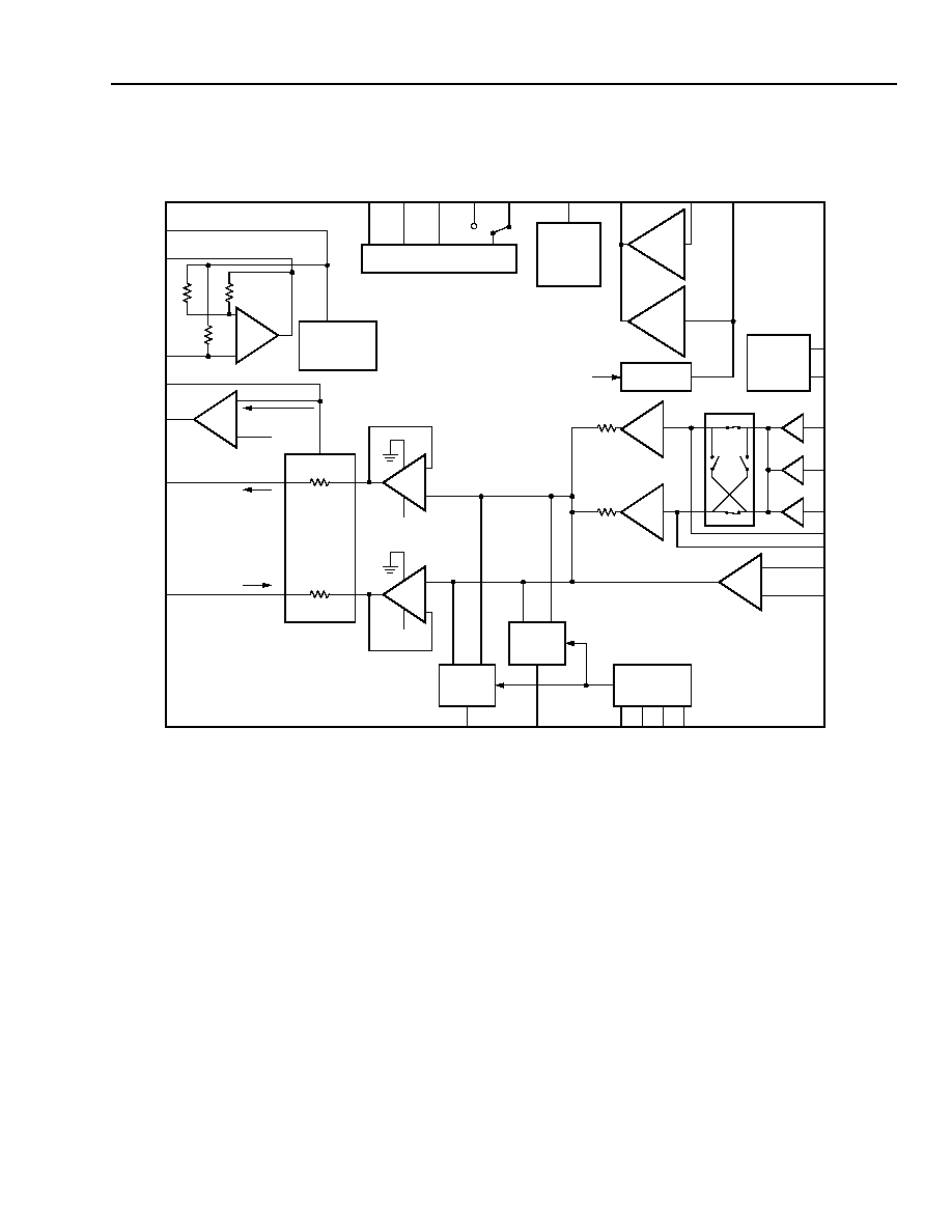
Architecture Diagram
12-3530.g (F)
Figure 1. Architecture Diagram
V
REF
VITR
TXI
ITR
VTX
PT
PR
ICM
TRGDET
CF2
OVH
CF1
FB2
FB1
POWER
AGND
V
CC
BGND V
BAT2
V
BAT1
V
PROG
NSTAT
RTFLT
DCOUT
1.5 V
BAND-GAP
REFERENCE
AAC
B = 20
OUT
(ITR/306)
TIP/RING
CURRENT
SENSE
+1
ITR
ITR
RFT
18
RFR
18
V
REG
�1
V
REG
RINGING
27.5x
PPM
2x
PARALLEL
DATA
INTERFACE
RING
IN
PPM
IN
BR
B0
B1
B2
X1
X1
RCVN
RCVP
CURRENT
LIMIT
AND
INRUSH
CONTROL
RING
LOOP
RECTIFIER
VITR
COMMON-
MODE
CURRENT
DETECTOR
TRIP
CLOSURE
V
REF
�
+
9215A GAIN = 4
+
�
+
�
�
+
GAIN
AX
9215G GAIN = 1
ac INTERFACE
Data Sheet
September 2001
Short-Loop Sine Wave Ringing SLIC
L9215A/G
8
Agere Systems Inc.
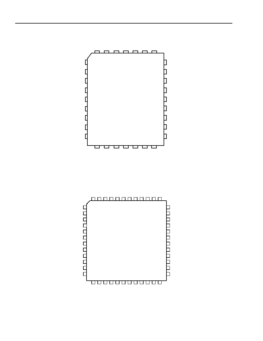
Pin Information
Figure 2. 32-Pin PLCC Diagram
Figure 3. 48-Pin MLCC Diagram
1
4
30
5
13
21
29
14
20
3
2
31
32
28
27
26
25
24
23
22
15
16
17
18
19
12
11
10
9
8
7
6
V
RE
F
AG
N
D
V
CC
V
BA
T
1
V
BA
T
2
BG
N
D
TR
G
D
ET
RTFLT
CF1
CF2
V
PROG
DCOUT
OVH
PPMIN
RING
IN
RCVN
RC
V
P
VI
T
R
NC
NS
T
A
T
TXI
VTX
IT
R
ICM
FB1
FB2
PT
PR
B2
B1
B0
BR
L9215A/G
32-PIN PLCC
1
3
4
6
7
8
9
10
11
12
2
48
46
45
44
43
42
41
40
38
37
47
13
16
17
18
19
20
21
22
23
24
14
36
33
32
31
30
29
28
27
26
25
35
B2
PT
FB1
PPM
IN
RING
INN
PR
RC
V
N
NS
T
A
T
RC
V
P
TXI
ITR
FB2
TR
G
D
ET
V
RE
F
V
BA
T
2
VITR
34
VTX
39
15
5
OVH
V
PROG
CF2
RTFLT
V
BA
T
1
IC
M
B1
BR
35
L9215A/G
48-PIN MLCC
DCOUT
CF1
B0
BG
ND
NC
NC
NC
NC
NC
NC
NC
NC
NC
NC
NC
NC
NC
NC
NC
NC
Vc
c
AG
ND
NC

Data Sheet
September 2001
Short-Loop Sine Wave Ringing SLIC
L9215A/G
Agere Systems Inc.
9
Pin Information
(continued)
Table 1. Pin Descriptions
32-Pin
PLCC
48-Pin
MLCC
Symbol Type
Name/Function
1
43
NSTAT
O
Loop Closure Detector Output--Ring Trip Detector Output. When
low, this logic output indicates that an off-hook condition exists or ring-
ing is tripped.
2
3, 4, 8, 11,
14, 17, 18,
21, 27, 28,
30, 32, 37,
39, 42, 44, 46
NC
--
No Connection.
3
45
VITR
O
Transmit ac Output Voltage. Output of internal AAC amplifier. This
output is a voltage that is directly proportional to the differential ac tip/
ring current.
4
47
RCVP
I
Receive ac Signal Input (Noninverting). This high-impedance input
controls to ac differential voltage on tip and ring. This node is a floating
input.
5
48
RCVN
I
Receive ac Signal Input (Inverting). This high-impedance input con-
trols to ac differential voltage on tip and ring. This node is a floating
input.
6
1
RING
IN
I
Power Ring Signal Input. ac-couple to a sine wave or lower crest fac-
tor low-voltage ring signal. The input here is amplified to provide the
full-power ring signal at tip and ring. This signal may be applied contin-
uously, even during nonringing states.
7
2
PPM
IN
I
Receive PPM Signal Input. ac-couple to a 12 kHz or 16 kHz PPM sig-
nal. The input here is amplified to provide the differential PPM voltage
on tip and ring. This signal may be applied continuously, even during
non-PPM modes.
8
5
OVH
I
Overhead Voltage Program Input. Connect a voltage source to this
point to program the overhead voltage. Voltage source may be external
or derived via a resistor divider from V
REF
. A programmable external
voltage source may be used to provide software control of the over-
head voltage. If a resistor or voltage source is not connected, the over-
head voltage will default to a nominal 6.0 V. If the default overhead is
desired, connect this pin to ground.
9
6
DCOUT
O
dc Output Voltage. This output is a voltage that is directly proportional
to the absolute value of the differential tip/ring current. This is used to
set ring trip threshold.
10
7
V
PROG
I
Current-Limit Program Input. Connect a voltage source to this point
to program the dc current limit. Voltage source may be external or
derived via a resistor divider from V
REF
. A programmable external volt-
age source may be used to provide software control of the current limit.
11
9
CF2
--
Filter Capacitor. Connect a capacitor from this node to ground.
12
10
CF1
--
Filter Capacitor. Connect a capacitor from this node to CF2.
13
12
RTFLT
--
Ring Trip Filter. Connect this lead to DCOUT via a resistor and to
AGND with a capacitor to filter the ring trip circuit to prevent spurious
responses. A single-pole filter is needed.
14
13
V
REF
O
SLIC Internal Reference Voltage. Output of internal 1.5 V reference
voltage.

Data Sheet
September 2001
Short-Loop Sine Wave Ringing SLIC
L9215A/G
10
Agere Systems Inc.
Pin Information
(continued)
Table 1. Pin Descriptions (continued)
32-Pin
PLCC
48-Pin
MLCC
Symbol Type
Name/Function
15
15
AGND
GND Analog Signal Ground.
16
16
V
CC
PWR Analog Power Supply. User choice of 5 V or 3.3 V nominal power or sup-
ply.
17
19
V
BAT1
PWR Battery Supply 1. High-voltage battery.
18
20
V
BAT2
PWR Battery Supply 2. Lower-voltage battery.
19
22
BGND
GND Battery Ground. Ground return for the battery supplies.
20
23
TRGDET
O
Tip/Ring Ground Detect. When high, this open collector output indicates
the presence of a ring ground or a tip ground. This supervision output may
be used in ground key or common-mode fault detection applications.
21
24
ICM
I
Common-Mode Current Sense. To program tip or ring ground sense
threshold, connect a resistor to V
CC
and connect a capacitor to AGND to fil-
ter 50/60 Hz. If unused, the pin is connected to ground.
22
25
FB2
--
Polarity Reversal Slowdown Capacitor. Connect a capacitor from this
node for controlling rate of battery reversal. If ramped battery reversal is
not desired, this pin is left open.
23
26
FB1
--
Polarity Reversal Slowdown Capacitor. Connect a capacitor from this
node for controlling rate of battery reversal. If ramped battery reversal is
not desired, this pin is left open.
24
29
PT
I/O
Protected Tip. The output drive of the tip amplifier and input to the loop
sensing circuit. Connect to loop through overvoltage and overcurrent pro-
tection.
25
31
PR
I/O
Protected Ring. The output drive of the ring amplifier and input to the loop
sensing circuit. Connect to loop through overvoltage and overcurrent pro-
tection.
26
33
B2
I
u
State Control Input. These pins have an internal 60 k
pull-up.
27
34
B1
28
35
B0
29
36
BR
30
38
ITR
I
Transmit Gain. Input to AX amplifier. Connect a resistor from this node to
VTX to set transmit gain. Gain shaping for termination impedance with a
COMBO I codec is also achieved with a network from this node to VTX.
31
40
VTX
O
ac Output Voltage. Output of internal AX amplifier. The voltage at this pin
is directly proportional to the differential tip/ring current.
32
41
TXI
I
ac/dc Separation. Input to internal AAC amplifier. Connect a 0.1
�
F capac-
itor from this pin to VTX.

Data Sheet
September 2001
Short-Loop Sine Wave Ringing SLIC
L9215A/G
Agere Systems Inc.
11
Operating States
Table 2. Control States
Table 3. Supervision Coding
B0
B1
B2
BR
State
1
1
0
1
Forward active
1
1
0
0
Forward active with PPM
1
0
0
1
Reverse active
1
0
0
0
Reverse active with PPM
1
1
1
1
On-hook transmission forward battery (in this state, the device will power up)
1
1
1
0
On-hook transmission with PPM forward battery
1
0
1
1
On-hook transmission reverse battery
1
0
1
0
On-hook transmission with PPM reverse battery
0
1
1
1
Scan
0
0
0
1
Disconnect
0
1
1
0
Ring
NSTAT
TRGDET
0 = off-hook or ring trip or TSD.
1 = on-hook and no ring trip and no
TSD or DISCONNECT state.
0 = no ring or tip ground
1 = ring or tip ground

Data Sheet
September 2001
Short-Loop Sine Wave Ringing SLIC
L9215A/G
12
Agere Systems Inc.
State Definitions
Forward Active
s
Pin PT is positive with respect to PR.
s
V
BAT2
is applied to tip/ring drive amplifiers.
s
Loop closure and common-mode detect are active.
s
Ring trip detector is turned off to conserve power.
s
PPM input is off.
s
Overhead is set to nominal 6.0 V for undistorted
transmission of 3.14 dBm into 900
and may be
increased via OVH.
Reverse Active
s
Pin PR is positive with respect to PT.
s
V
BAT2
is applied to tip/ring drive amplifiers.
s
Loop closure and common-mode detect are active.
s
Ring trip detector is turned off to conserve power.
s
PPM input is off.
s
Overhead is set to nominal 6.0 V for undistorted
transmission of 3.14 dBm into 900
and may be
increased via OVH.
Forward Active with PPM
s
Pin PT is positive with respect to PR.
s
V
BAT2
is applied to tip/ring drive amplifiers.
s
Loop closure and common-mode detect are active.
s
Ring trip detector is turned off to conserve power.
s
PPM input is on.
s
Overhead is set to nominal 6.0 V for undistorted
transmission of 3.14 dBm into 900
and may be
increased via OVH to accommodate higher-voltage
meter pulse signals.
Reverse Active with PPM
s
Pin PR is positive with respect to PT.
s
V
BAT2
is applied to tip/ring drive amplifiers.
s
Loop closure and common-mode detect are active.
s
Ring trip detector is turned off to conserve power.
s
PPM input is on.
s
Overhead is set to nominal 6.0 V for undistorted
transmission of 3.14 dBm into 900
and may be
increased via OVH to accommodate higher-voltage
meter pulse signals.
Scan
s
Except for loop closure, all circuits (including ring trip
and common-mode detector) are powered down.
s
On-hook transmission is disabled.
s
Pin PT is positive with respect to PR and V
BAT1
is
applied to tip/ring.
s
The tip-to-ring on-hook differential voltage will be
typ-
ically
between �44 V and �51 V with a �70 V primary
battery.
On-Hook Transmission
--
Forward Battery
s
Pin PT is positive with respect to PR.
s
V
BAT1
is applied to tip/ring drive amplifiers.
s
Supervision circuits, loop closure, and common-
mode detect are active.
s
Ring trip detector is turned off to conserve power.
s
On-hook transmission is allowed.
s
The tip-to-ring on-hook differential voltage will be
between �41 V and �49 V with a �70 V primary bat-
tery.
s
PPM is off.

Data Sheet
September 2001
Short-Loop Sine Wave Ringing SLIC
L9215A/G
Agere Systems Inc.
13
State Definitions
(continued)
On-Hook Transmission with PPM
--
Forward
Battery
s
Pin PT is positive with respect to PR.
s
V
BAT1
is applied to tip/ring drive amplifiers.
s
Supervision circuits, loop closure, and common-
mode detect are active.
s
Ring trip detector is turned off to conserve power.
s
On-hook transmission is allowed.
s
The tip-to-ring on-hook differential voltage will be
between �41 V and �49 V with a �70 V primary bat-
tery.
s
PPM is on.
On-Hook Transmission
--
Reverse Battery
s
Pin PR is positive with respect to PT.
s
V
BAT1
is applied to tip/ring drive amplifiers.
s
Supervision circuits, loop closure, and common-
mode detect are active.
s
Ring trip detector is turned off to conserve power.
s
On-hook transmission is allowed.
s
The tip-to-ring on-hook differential voltage will be
between �41 V and �49 V with a �70 V primary bat-
tery.
s
PPM is off.
On-Hook Transmission with PPM
--
Reverse
Battery
s
Pin PR is positive with respect to PT.
s
V
BAT1
is applied to tip/ring drive amplifiers.
s
Supervision circuits, loop closure, and common-
mode detect are active.
s
Ring trip detector is turned off to conserve power.
s
On-hook transmission is allowed.
s
The tip-to-ring on-hook differential voltage will be
between �41 V and �49 V with a �70 V primary bat-
tery.
s
PPM is on.
Disconnect
s
The tip/ring amplifiers and all supervision are turned
off.
s
The SLIC goes into a high-impedance state.
s
NSTAT is forced high (on-hook).
Ring
s
Power ring signal is applied to tip and ring.
s
Input waveform at RING
IN
is amplified.
s
Ring trip supervision and common-mode current
supervision are active; loop closure is inactive.
s
Overhead voltage is reduced to typically 4 V, regard-
less of programming on OVH, and current limit set at
V
PROG
is disabled.
s
Current is limited by saturation current of the amplifi-
ers themselves, typically 100 mA at 125 �C.
Thermal Shutdown
s
Not controlled via truth table inputs.
s
NSTAT is forced low (off-hook) during this state
s
This mode is caused by excessive heating of the
device, such as may be encountered in an extended
power cross situation.

Data Sheet
September 2001
Short-Loop Sine Wave Ringing SLIC
L9215A/G
14
Agere Systems Inc.
Absolute Maximum Ratings
(@ T
A
= 25 �C)
Stresses in excess of the absolute maximum ratings can cause permanent damage to the device. These are abso-
lute stress ratings only. Functional operation of the device is not implied at these or any other conditions in excess
of those given in the operational sections of the data sheet. Exposure to absolute maximum ratings for extended
periods can adversely affect device reliability.
Note: The IC can be damaged unless all ground connections are applied before, and removed after, all other connections. Furthermore, when
powering the device, the user must guarantee that no external potential creates a voltage on any pin of the device that exceeds the
device ratings. For example, inductance in a supply lead could resonate with the supply filter capacitor to cause a destructive overvoltage.
Table 4. Recommended Operating Characteristics
Table 5. Thermal Characteristics
1. This parameter is not tested in production. It is guaranteed by design and device characterization.
2. Airflow, PCB board layers, and other factors can greatly affect this parameter.
Parameter
Symbol
Min
Typ
Max
Unit
dc Supply (V
CC
) --
�0.5
--
7.0
V
Battery Supply (V
BAT1
)
--
--
--
�80
V
Battery Supply (V
BAT2
)
--
--
--
V
BAT1
V
Logic Input Voltage
--
�0.5
--
V
CC
+ 0.5
V
Logic Output Voltage
--
�0.5
--
V
CC
+ 0.5
V
Operating Temperature Range
--
�40
--
125
�C
Storage Temperature Range
--
�40
--
150
�C
Relative Humidity Range
--
5
--
95
%
Ground Potential Difference (BGND to AGND)
--
--
--
�1
V
PT or PR Fault Voltage (dc)
V
PT
, V
PR
V
BAT
� 5
--
3
V
PT or PR Fault Voltage (10 x 1000
�
s)
V
PT
, V
PR
V
BAT
� 15
--
15
V
Parameter
Min
Typ
Max
Unit
5 V dc Supplies (V
CC
)
--
5.0
5.25
V
3 V dc Supplies (V
CC
)
3.13
3.3
--
V
High Office Battery Supply (V
BAT1
)
�60
�70
�75
V
Auxiliary Office Battery Supply (V
BAT2
)
�12
--
V
BAT1
V
Operating
Temperature
Range
�40 25
85
�C
Parameter
Min
Typ
Max
Unit
Thermal Protection Shutdown (T
jc
)
150
165
--
�
C
32-pin PLCC Thermal Resistance Junction to Ambient (
JA
)
1, 2
:
Natural Convection 2S2P Board
Natural Convection 2S0P Board
Wind Tunnel 100 Linear Feet per Minute (LFPM) 2S2P Board
Wind Tunnel 100 Linear Feet per Minute (LFPM) 2S0P Board
--
--
--
--
35.5
50.5
31.5
42.5
--
--
--
--
�
C/W
�
C/W
�
C/W
�
C/W
48-pin MLCC Thermal Resistance Junction to Ambient (
JA
)
1, 2
--
38
--
�
C/W

Data Sheet
September 2001
Short-Loop Sine Wave Ringing SLIC
L9215A/G
Agere Systems Inc.
15
Electrical Characteristics
Table 6
.
Environmental Characteristics
1. Not to exceed 26 grams of water per kilogram of dry air.
Table 7. 5 V Supply Currents
V
BAT1
= �70 V, V
BAT2
= �21 V, V
CC
= 5 V.
Table 8. 5 V Powering
V
BAT1
= �70 V, V
BAT2
= �21 V, V
CC
= 5 V.
Parameter
Min
Typ
Max
Unit
Temperature Range
�40
--
85
�C
Humidity Range
1
5
--
95
1
%RH
Parameter
Min
Typ
Max
Unit
Supply Currents (scan state; no loop current):
I
VCC
I
VBAT1
I
VBAT2
--
--
--
4.30
0.24
3
4.80
0.35
6
mA
mA
�
A
Supply Currents (forward/reverse active; no loop current, with or without PPM,
V
BAT2
applied):
I
VCC
I
VBAT1
I
VBAT2
--
--
--
5.95
25
1.2
7.0
85
1.40
mA
�
A
mA
Supply Currents (on-hook transmission mode; no loop current, with or without
PPM, V
BAT1
applied):
I
VCC
I
VBAT1
I
VBAT2
--
--
--
6.0
1.5
1.5
7.0
1.9
6
mA
mA
�
A
Supply Currents (disconnect mode):
I
VCC
I
VBAT1
I
VBAT2
--
--
--
2.7
15
3.5
3.75
110
25
mA
�
A
�
A
Supply Currents (ring mode; no load):
I
VCC
I
VBAT1
I
VBAT2
--
--
--
5.9
1.8
2
6.5
2.2
6
mA
mA
�
A
Parameter
Min
Typ
Max
Unit
Power Dissipation (scan state; no loop current)
--
38
46
mW
Power Dissipation (forward/reverse active; no loop current, with or without PPM)
--
57
64
mW
Power Dissipation (on-hook transmission mode; no loop current, with or without
PPM, V
BAT1
applied)
--
135
165
mW
Power Dissipation (disconnect mode)
--
14
23
mW
Power Dissipation (ring mode; no load)
--
156
184
mW

Data Sheet
September 2001
Short-Loop Sine Wave Ringing SLIC
L9215A/G
16
Agere Systems Inc.
Electrical Characteristics
(continued)
Table 9. 3.3 V Supply Currents
V
BAT1
= �70 V, V
BAT2
= �21 V, V
CC
= 3.3 V.
Table 10. 3.3 V Powering
V
BAT1
= �70 V, V
BAT2
= �21 V, V
CC
= 3.3 V.
Parameter
Min
Typ
Max
Unit
Supply Currents (scan state; no loop current):
I
VCC
I
VBAT1
I
VBAT2
--
--
--
3.2
0.24
3
3.6
0.35
6
mA
mA
�
A
Supply Currents (forward/reverse active; no loop current, with/without PPM,
V
BAT2
applied):
I
VCC
I
VBAT1
I
VBAT2
--
--
--
4.8
25
1.2
5.7
85
1.4
mA
�
A
mA
Supply Currents (on-hook transmission mode; no loop current, with/without
PPM, V
BAT1
applied):
I
VCC
I
VBAT1
I
VBAT2
--
--
--
4.9
1.5
1.5
5.7
1.9
6
mA
mA
�
A
Supply Currents (disconnect mode):
I
VCC
I
VBAT1
I
VBAT2
--
--
--
1.8
8
2
2.5
110
25
mA
�
A
�
A
Supply Currents (ring mode; no loop current):
I
VCC
I
VBAT1
I
VBAT2
--
--
--
4.70
1.8
2
5.4
2.2
6
mA
mA
�
A
Parameter
Min
Typ
Max
Unit
Power Dissipation (scan state; no loop current)
--
27
36.5
mW
Power Dissipation (forward/reverse active; no loop current, with/without PPM,
V
BAT2
applied)
--
42
53
mW
Power Dissipation (on-hook transmission mode; no loop current, with/without
PPM, V
BAT1
applied)
--
121
151
mW
Power Dissipation (disconnect mode)
--
6.5
15
mW
Power Dissipation (ring mode; no loop current)
--
141
172
mW

Data Sheet
September 2001
Short-Loop Sine Wave Ringing SLIC
L9215A/G
Agere Systems Inc.
17
Electrical Characteristics
(continued)
Table 11. 2-Wire Port
Parameter
Min
Typ
Max
Unit
Tip or Ring Drive Current = dc + Longitudinal + Signal Currents + PPM
105
--
--
mAp
Tip or Ring Drive Current = Ringing + Longitudinal
65
--
--
mAp
Signal Current
10
--
--
mArms
Longitudinal Current Capability per Wire (Longitudinal current is indepen-
dent of dc loop current.)
8.5
15
--
mArms
PPM Signal Current = 1.25 V
MAX
into 200
ac
6.25
--
--
mArms
Ringing Current (R
LOAD
= 1386
+ 40
�
F)
29
--
--
mArms
Ringing Current Limit (R
LOAD
= 100
)
--
--
50
mAp
dc Loop Current--I
LIM
(R
LOOP
= 100
):
Programming Range (V
CC
= 5 V)
Programming Range (V
CC
= 3.3 V)
Voltage at V
PROG
15
15
0.194
--
--
--
70
45
1.01
mA
mA
V
dc Current Variation (current limit 22 mA to 28 mA)
--
--
�8
%
dc Current Variation (current limit 70 mA)
--
--
�10
%
dc Feed Resistance (does not include protection resistors)
--
50
--
Open Loop Voltages:
Scan Mode:
|V
BAT1
| > 51 V |V
TIP
| � |V
RING
|
PR to Battery Ground
PT to Battery Ground
OHT Mode:
|V
BAT1
| > 51 V (V
OH
= 0 V) |V
TIP
| � |V
RING
|
PR to Battery Ground
PT to Battery Ground
Active Mode (V
OH
= 0 V):
|PT � PR| � |V
BAT2
|
Ring Mode:
|PT � PR| � |V
BAT1
|
44
--
--
41
--
--
5.65
--
51
--
--
49
--
--
6.0
4.0
--
56.5
56.5
--
56.5
56.5
6.5
--
V
V
V
V
V
V

Data Sheet
September 2001
Short-Loop Sine Wave Ringing SLIC
L9215A/G
18
Agere Systems Inc.
Electrical Characteristics
(continued)
Table 11. 2-Wire Port (continued)
Table 12. Analog Pin Characteristics
Parameter
Min
Typ
Max
Unit
Loop Closure Threshold:
Active/On-hook Transmission Modes
Scan Mode
--
--
10.5
11.5
--
--
mA
mA
Loop Closure Threshold Hysteresis:
V
CC
= 5 V
V
CC
= 3.3 V
--
--
2
1
--
--
mA
mA
Ground Key:
Differential Detector Threshold
Detection
5
50
8
--
10
--
mA
ms
Longitudinal to Metallic Balance at PT/PR
Test Method: Q552 (11/96) Section 2.1.2 and
IEEE
�
455:
300 Hz to 600 Hz
600 Hz to 3.4 kHz
52
52
--
--
--
--
dB
dB
Metallic to Longitudinal (harm) Balance:
200 Hz to 1000 Hz
100 Hz to 4000 Hz
40
40
--
--
--
--
dB
dB
PSRR 500 Hz--3000 Hz:
V
BAT1
, V
BAT2
V
CC
(5 V operation)
45
35
--
--
--
--
dB
dB
Parameter
Min
Typ
Max
Unit
TXI (input impedance)
--
100
--
k
Output Offset (VTX)
Output Offset (VITR)
Output Drive Current (VTX)
Output Drive Current (VITR)
Output Voltage Swing:
Maximum (VTX, VITR)
Minimum (VTX)
Minimum (VITR)
Output Short-circuit Current
Output Load Resistance
Output Load Capacitance
--
--
�300
�10
AGND
AGND + 0.25
AGND + 0.35
--
10
--
--
--
--
--
--
--
--
--
--
20
�10
�100
--
--
V
CC
V
CC
� 0.5
V
CC
� 0.4
�50
--
--
mV
mV
�
A
�
A
V
V
V
mA
k
pF
RCVN and RCVP:
Input Voltage Range (V
CC
= 5 V)
Input Voltage Range (V
CC
= 3.3 V)
Input Bias Current
0
0
--
--
--
0.05
V
CC
� 0.5
V
CC
� 0.3
--
V
V
�
A
Differential PT/PR Current Sense (DCOUT):
Gain (PT/PR to DCOUT)
Offset Voltage at I
LOOP
= 0
--
�20
67
--
--
20
V/A
mV

Data Sheet
September 2001
Short-Loop Sine Wave Ringing SLIC
L9215A/G
Agere Systems Inc.
19
Electrical Characteristics
(continued)
Table 13. ac Feed Characteristics
1. Set externally either by discrete external components or a third- or fourth-generation codec. Any complex impedance R1 + R2 || C between
150
and 1400
can be synthesized.
2. This parameter is not tested in production. It is guaranteed by design and device characterization.
3. VITR transconductance depends on the resistor from ITR to VTX. This gain assumes an ideal 4750
, the recommended value. Positive cur-
rent is defined as the differential current flowing from PT to PR.
Parameter
Min
Typ
Max
Unit
ac Termination Impedance
1
150
600
1400
Total Harmonic Distortion (200 Hz--4 kHz)
2
:
Off-hook
On-hook
--
--
--
--
0.3
1.0
%
%
Transmit Gain (f = 1004 Hz, 1020 Hz, current limit)
3
:
PT/PR Current to VITR
300 � 3%
300
300 + 3%
V/A
Receive Gain, f = 1004 Hz, 1020 Hz Open Loop:
RCVP or RCVN to PT--PR (gain of 8 option, L9215A)
RCVP or RCVN to PT--PR (gain of 2 option, L9215G)
7.76
1.94
8
2
8.24
2.06
--
--
Gain vs. Frequency (transmit and receive)
2
600
Termination,
1004 Hz, 1020 Hz Reference:
200 Hz--300 Hz
300 Hz--3.4 kHz
3.4 kHz--20 kHz
20 kHz--266 kHz
�0.3
�0.05
�3.0
--
0
0
0
--
0.05
0.05
0.05
2.0
dB
dB
dB
dB
Gain vs. Level (transmit and receive)
2
0 dBV Reference:
�55 dB to +3.0 dB
�0.05
0
0.05
dB
Idle-channel Noise (tip/ring) 600
Termination:
Psophometric
C-Message
3 kHz Flat
--
--
--
�82
8
--
�77
13
20
dBmp
dBrnC
dBrn
Idle-channel Noise (VTX) 600
Termination:
Psophometric
C-Message
3 kHz Flat
--
--
--
�82
8
--
�77
13
20
dBmp
dBrnC
dBrn

Data Sheet
September 2001
Short-Loop Sine Wave Ringing SLIC
L9215A/G
20
Agere Systems Inc.
Electrical Characteristics
(continued)
Table 14. Logic Inputs and Outputs (V
CC
= 5 V)
Table 15. Logic Inputs and Outputs (V
CC
= 3.3 V)
Parameter
Symbol
Min
Typ
Max
Unit
Input Voltages:
Low Level
High Level
V
IL
V
IH
�0.5
2.0
0.4
2.4
0.7
V
CC
V
V
Input Current:
Low Level (V
CC
= 5.25 V, V
I
= 0.4 V)
High Level (V
CC
= 5.25 V, V
I
= 2.4 V)
I
IL
I
IH
--
--
--
--
�50
�50
�
A
�
A
Output Voltages (open collector with internal pull-up resistor):
Low Level (V
CC
= 4.75 V, I
OL
= 200
�
A)
High Level (V
CC
= 4.75 V, I
OH
= �20
�
A)
V
OL
V
OH
0
2.4
0.2
--
0.4
V
CC
V
V
Parameter
Symbol
Min
Typ
Max
Unit
Input Voltages:
Low Level
High Level
V
IL
V
IH
�0.5
2.0
0.2
2.5
0.5
V
CC
V
V
Input Current:
Low Level (V
CC
= 3.46 V, V
I
= 0.4 V)
High Level (V
CC
= 3.46 V, V
I
= 2.4 V)
I
IL
I
IH
--
--
--
--
�50
�50
�
A
�
A
Output Voltages (open collector with internal pull-up resistor):
Low Level (V
CC
= 3.13 V, I
OL
= 200
�
A)
High Level (V
CC
= 3.13 V, I
OH
= �5
�
A)
V
OL
V
OH
0
2.2
0.2
--
0.5
V
CC
V
V

Data Sheet
September 2001
Short-Loop Sine Wave Ringing SLIC
L9215A/G
Agere Systems Inc.
21
Electrical Characteristics
(continued)
Table 16. Ringing Specifications
Table 17. Ring Trip
Ringing will not be tripped by the following loads:
s
10 k
resistor in parallel with a 6 �F capacitor applied across tip and ring. Ring frequency = 17 Hz to 23 Hz.
s
100
resistor in series with a 2 �F capacitor applied across tip and ring. Ring frequency = 17 Hz to 23 Hz.
Table 18. PPM
*
PPM signal should be ac coupled through 10 nF.
Parameter
Min
Typ
Max
Unit
RING
IN
(This input is ac coupled through 0.47 �F.):
Input Voltage Swing
Input Impedance
0
--
--
100
V
CC
--
V
k
Ring Signal Isolation:
PT/PR to VITR
Ring Mode
--
60
--
dB
Ring Signal Isolation:
RING
IN
to PT/PR
Nonring Mode
--
80
--
dB
Ringing Voltage (5 REN 1380
+ 40 �F load, 100
loop, 2 x 50
protection
resistors, �70 V battery)
40
--
--
Vrms
Ringing Voltage (3 REN 2310
+ 24 �F load, 250
loop, 2 x 50
protection
resistors, �70 V battery)
40
--
--
Vrms
Ring Signal Distortion:
5 REN 1380
, 40 �F Load, 100
Loop
3 REN 2310
, 24 �F Load, 250
Loop
--
--
3
3
--
--
%
%
Differential Gain:
RING
IN
to PT/PR--No Load
--
55
--
--
Parameter Min
Typ
Max
Unit
Ring Trip (NSTAT = 0): Loop Resistance (total)
100
--
600
Ring Trip (NSTAT = 1): Loop Resistance (total)
--
--
10
k
Trip Time (f = 20 Hz)
--
--
100
ms
Parameter Min
Typ
Max
Unit
PPM Source*:
Frequency (f1)
Frequency (f2)
Input Signal
11.88
15.80
0
12
16
1.1
12.12
16.20
1.25
kHz
kHz
Vrms
Input Impedance
--
50
--
k
Signal Gain (2.2 Vrms maximum at PT/PR)
5.5
6
6.5
dB
Isolation
--
60
--
dB
Harmonic Distortion
--
--
5
%
Data Sheet
September 2001
Short-Loop Sine Wave Ringing SLIC
L9215A/G
22
Agere Systems Inc.
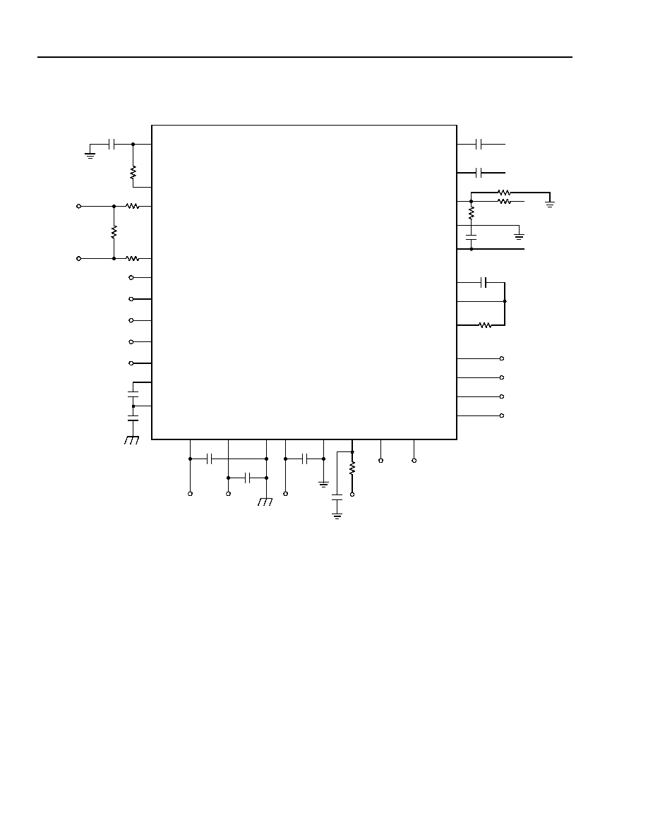
Test Configurations
12-3531.E (F)
Figure 4. Basic Test Circuit
V
BAT2
V
BAT1
BGND V
CC
AGND
ICM TRGDET
0.1
�
F
0.1
�
F
0.1
�
F
RTFLT
DCOUT
PR
PT
OVH
V
PROG
V
REF
0.1
�
F
383 k
30
30
CF1
CF2
BR
B0
B1
B2
0.1
�
F
10 nF
RING
IN
PPM
IN
VITR
RCVP
RCVN
ITR
VTX
TXI
V
BAT2
V
BAT1
V
CC
0.47
�
F
R
LOOP
100
/600
TIP
RING
FB2
FB1
0.1
�
F
L9215
NSTAT
BR
B0
B1
B2
4750
0.1
�
F
VITR
RCV
RING
IN
PPM
IN
82.3 k
0.1
�
F
60.4 k
0.1
�
F
26.7 k
69.8 k
RCV
V
CC
BASIC TEST
CIRCUIT
L9215
BASIC TEST
CIRCUIT
Data Sheet
September 2001
Short-Loop Sine Wave Ringing SLIC
L9215A/G
Agere Systems Inc.
23
Test Configurations
(continued)
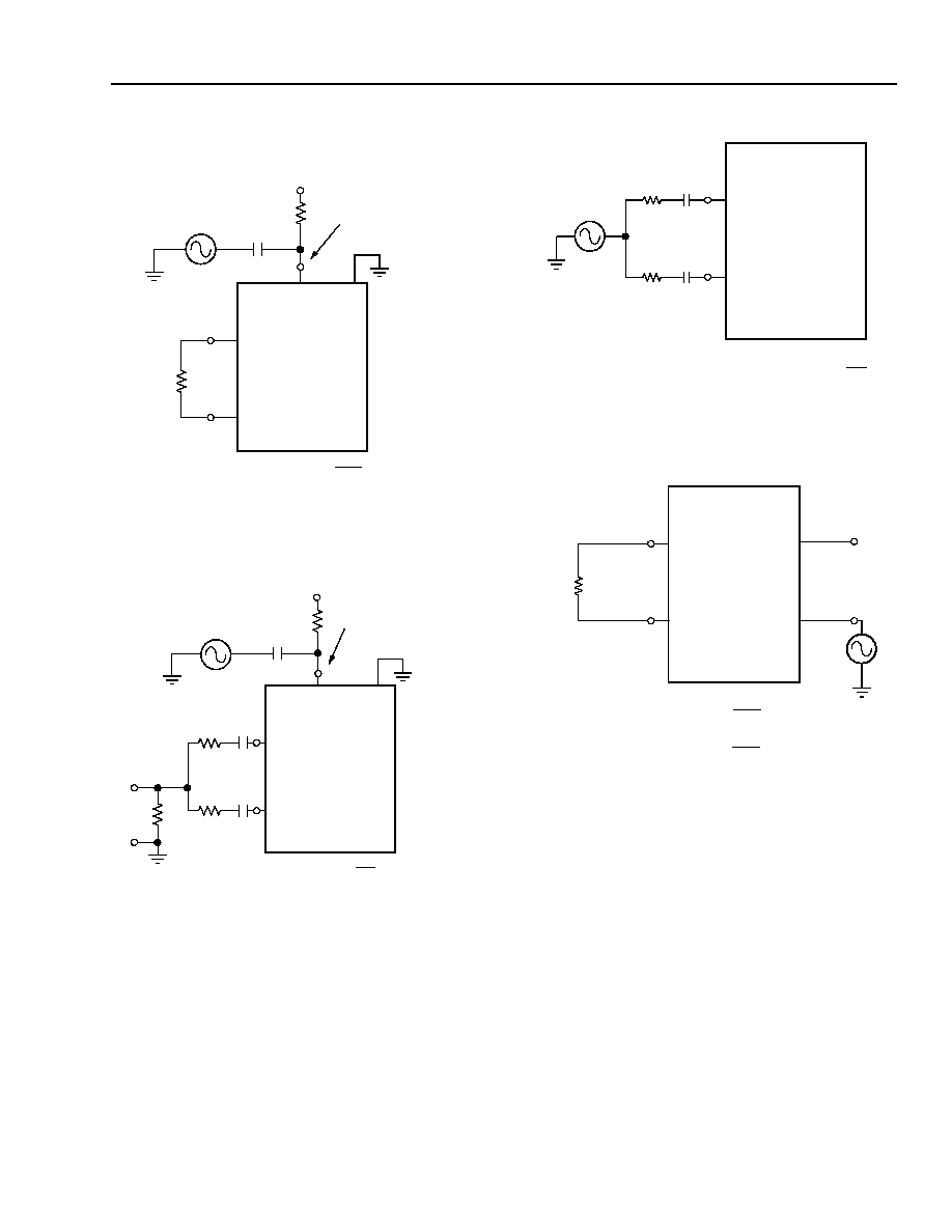
12-2582.c (F)
Figure 5. Metallic PSRR
12-2583.b (F)
Figure 6. Longitudinal PSRR
12-2584.c (F)
Figure 7. Longitudinal Balance
12-2587.G (F)
Figure 8. ac Gains
V
S
4.7
�
F
100
V
BAT
OR
V
CC
DISCONNECT
V
T/R
V
BAT
OR
V
CC
TIP
RING
BASIC
TEST CIRCUIT
+
�
PSRR = 20log
V
S
V
T/R
600
BYPASS CAPACITOR
V
S
4.7
�
F
100
V
BAT
OR
V
CC
DISCONNECT
BYPASS CAPACITOR
56.3
V
BAT
OR V
CC
TIP
RING
BASIC
TEST CIRCUIT
PSRR = 20log
V
S
V
M
67.5
10
�
F
10
�
F
67.5
V
M
+
�
TIP
RING
BASIC
TEST CIRCUIT
LONGITUDINAL BALANCE = 20log
V
S
V
M
368
100
�
F
100
�
F
368
V
M
+
�
V
S
PT
PR
BASIC
TEST CIRCUIT
600
V
T/R
+
�
G
XMT
=
V
XMT
V
T/R
G
RCV
=
V
T/R
V
RCV
RCV
V
S
VITR
RCV

Data Sheet
September 2001
Short-Loop Sine Wave Ringing SLIC
L9215A/G
24
Agere Systems Inc.
Applications
Power Control
Under normal device operating conditions, power dissi-
pation on the device must be controlled to prevent the
device temperature from rising above the thermal shut-
down and causing the device to shut down. Power dis-
sipation is highest with higher battery voltages, higher
current limit, and under shorter dc loop conditions.
Additionally, higher ambient temperature will also
reduce thermal margin.
To support required power ringing voltages, this device
is meant to operate with a high-voltage primary battery
(�65 V to �75 V typically). Thus, power control is nor-
mally achieved by use of the battery switch and an aux-
iliary lower absolute voltage battery. Operating
temperature range, maximum current limit, maximum
battery voltage, minimum dc loop length and protection
resistors values, airflow, and number of PC board lay-
ers will influence the overall thermal performance. The
following example illustrates typical thermal design
considerations.
The thermal resistance of the 32-pin PLCC package is
typically 50.5
�
C/W, which is representative of the natu-
ral airflow as seen in a typical switch cabinet with a
two-layer board.
The L9215 will enter thermal shutdown at a minimum
temperature of 150
�
C. The thermal design should
ensure that the SLIC does not reach this temperature
under normal operating conditions.
For this example, assume a maximum ambient operat-
ing temperature of 85
�
C, a maximum current limit of
30 mA, a maximum battery of �70 V, and an auxiliary
battery of �21 V. Assume a (worst-case) minimum dc
loop of 20
of wire resistance, 30
protection resis-
tors, and 200
for the handset. Additionally, include
the effects of parameter tolerance.
1. T
TSD
� T
AMBIENT(max)
= allowed thermal rise.
150 �C � 85 �C = 65 �C.
2. Allowed thermal rise = package thermal
impedance
�
SLIC power dissipation.
65 �C = 50.5 �C/W
�
SLIC power dissipation
SLIC power dissipation (P
D
) = 1.29 W.
Thus, if the total power dissipated in the SLIC is less
than 1.29 W, it will not enter the thermal shutdown
state. Total SLIC power is calculated as:
Total P
D
= maximum battery
�
maximum current
limit + SLIC quiescent power.
For the L9215, the worst-case SLIC on-hook active
power is 76.4 mW. Thus,
Total off-hook power = (I
LOOP
)(current-limit
tolerance)*(V
BATAPPLIED
) + SLIC on-hook power
Total off-hook power = (0.030 A)(1.08) * (21) +
76.4 mW
Total off-hook power = 756.8 mW
The power dissipated in the SLIC is the total power dis-
sipation less the power that is dissipated in the loop.
SLIC P
D
= total power � loop power
Loop off-hook power = (I
LOOP
* 1.08)
2
�
(R
LOOP(dc)
min + 2R
HANDSET
)
Loop off-hook power = (0.030 A)(1.08)
2
�
(20
+
60
+ 200
)
Loop off-hook power = 293.9 mW
SLIC off-hook power = Total off-hook power � loop
off-hook power
SLIC off-hook power = 756.8 mW � 293.9 mW
SLIC off-hook power = 462.9 mW < 1.29 W
Thus, under the worst-case normal operating condi-
tions of this example, the thermal design, using the
auxiliary, is adequate to ensure the device is not driven
into thermal shutdown under worst-case operating con-
ditions.
dc Loop Current Limit
In the active modes, dc current limit is programmable
via an applied voltage source at the device's V
PROG
control input. The voltage source may be an external
voltage source or derived via a resistor divider network
from the V
REF
SLIC output or an external voltage
source. A programmable external voltage source may
be used to provide software control of the loop current
limit. The loop current limit (I
LIM
) is related to the V
PROG
voltage at the onset of current limit by:
I
LIM
(mA) = 67 (mA/V) * V
PROG
(V)
Note that there is a 12.5 k
slope to the I/V character-
istic in the current-limit region; thus, once in current
limit, the actual loop current will increase slightly, as
loop length decreases.

Data Sheet
September 2001
Short-Loop Sine Wave Ringing SLIC
L9215A/G
Agere Systems Inc.
25
Applications
(continued)
dc Loop Current Limit
(continued)
Note that the overall current-limit accuracy achieved
will not only be affected by the specified accuracy of
the internal SLIC current-limit circuit (accuracy associ-
ated with the 67 term), but also by the accuracy of the
voltage source and the accuracy of any external resis-
tor divider network used and voltage offsets due to the
specified input bias current. Tolerance of the current
limit is �8%. If a resistor divider from V
REF
is used, it is
recommended that the sum of the two resistors be
greater than 100 k
.
The above equations describe the active mode steady-
state current-limit response. There will be a transient
response of the current-limit circuit upon an on- to off-
hook transition. Typical active mode transient current-
limit response is given in Table 19.
Table 19. Typical Active Mode On- to Off-Hook Tip/
Ring Current-Limit Transient Response
Overhead Voltage
Active Mode
Overhead is programmable in the active mode via an
applied voltage source at the device's OVH control
input. The voltage source may be an external voltage
source or derived via a resistor divider network from
the V
REF
SLIC output or an external voltage source. A
programmable external voltage source may be used to
provide software control of the overhead voltage. The
overhead voltage (V
OH
) is related to the OVH voltage
by:
V
OH
= 6.0 V + 5 * V
OVH
(V)
Overall accuracy is determined by the accuracy of the
voltage source and the accuracy of any external resis-
tor divider network used and voltage offsets due to the
specified input bias current. If a resistor divider from
V
REF
is used, a lower magnitude resistor will give a
more accurate result due to a lower offset associated
with the input bias current; however, lower value resis-
tors will also draw more power from V
REF
.
Note that a default overhead voltage of 6.0 V is
achieved by shorting input pin OVH to analog ground.
The default overhead provides sufficient headroom for
an on-hook transmission of a 3.14 dBm signal into
900
.
Overhead voltage may need to be increased to accom-
modate on-hook transmission of higher-voltage sig-
nals, such as meter pulse. The following example is
meant to illustrate the design procedure that can be fol-
lowed.
Assume we need on-hook transmission of a 1.0 Vrms
meter pulse into 200
. Further, assume 50
protec-
tion resistors are used.
V
OH
= 6.0 V + (1+ [2 * Rp]/200) * Vpeak
V
OH
= 6.0 + (1+ [2 * 50]/200) * 1 (1.414)
V
OH
= 8.121 V
Parameter
Value
Unit
dc Loop Current:
Active Mode
R
LOOP
= 100
On- to Off-hook
Transition t < 5 ms
I
LIM
+ 60
mA
dc Loop Current:
Active Mode
R
LOOP
= 100
On- to Off-hook
Transition t < 50 ms
I
LIM
+ 20
mA
dc Loop Current:
Active Mode
R
LOOP
= 100
On- to Off-hook
Transition t < 300 ms
I
LIM
mA

Data Sheet
September 2001
Short-Loop Sine Wave Ringing SLIC
L9215A/G
26
Agere Systems Inc.
Applications
(continued)
Overhead Voltage
(continued)
Active Mode (continued)
Adding 0.5 V for tolerance, the overhead needs to be
increased to (8.121 V + 0.5 V) = 8.621 V to allow for an
undistorted on-hook transmission of a 1 Vrms meter
pulse into 200
. This is done by applying voltage to
pin V
OH
.
V
OH
(V) = 6.0 V + 5 * V
OVH
(V)
8.621 V = 6 V + 5 * V
OVH
V
OVH
= 0.5242 V
Thus, a nominal 0.5242 V is applied to pin V
OVH
to
increase the overhead.
Scan Mode
If the magnitude of the primary battery is greater than
51 V, the magnitude of the open loop tip-to-ring open
loop voltage is clamped typically between 44 V and
51 V. If the magnitude of the primary battery is less
than a nominal 51 V, the overhead voltage will track the
magnitude of the battery voltage, i.e., the magnitude of
the open circuit tip-to-ring voltage will be 4 V to 6 V less
than battery. In the scan mode, overhead is unaffected
by V
OVH
.
On-Hook Transmission Mode
If the magnitude of the primary battery is greater than
51 V, the magnitude of the open loop tip-to-ring open
loop voltage is clamped typically between 41 V and
49 V. If the magnitude of the primary battery is less
than a nominal 51 V, the overhead voltage will track the
magnitude of the battery voltage, i.e., the magnitude of
the open circuit tip-to-ring voltage will be 6 V to 8 V less
than battery. In the scan mode, overhead is unaffected
by V
OVH
.
Ring Mode
In the ring mode, to maximize ringing loop length, the
overhead is decreased to the saturation of the tip ring
drive amplifiers, a nominal 4 V. The tip-to-ground volt-
age is 1 V, and the ring to V
BAT1
voltage is 3 V. In the
ring mode, overhead is unaffected by V
OVH
.
During the ring mode, to conserve power the receive
input at RCVN/RCVP is deactivated. During the ring
mode, to conserve power, the ACC amplifier in the
transmit direction at VITR is deactivated. However, if
the AX amplifier at VTX is active during the ring mode,
differential ring current may be sensed at VTX during
the ring mode.
Loop Range
The dc loop range is calculated using:
R
L
=
� 2R
P
� R
DC
V
BAT2
is typically applied under off-hook conditions for
power conservation and SLIC thermal considerations.
The L9215 is intended for short-loop applications and,
therefore, will always be in current limit during off-hook
conditions. However, note that the ringing loop length
rather than the dc loop length, will be the factor to
determine operating loop length.
Battery Reversal Rate
The rate of battery reverse is controlled or ramped by
capacitors FB1 and FB2. A chart showing FB1 and FB2
values versus typical ramp time is given below. Leave
FB1 and FB2 open if it is not desired to ramp the rate of
battery reversal.
Table 20. FB1 and FB2 Values vs. Typical Ramp
Time
C
FB1
and C
FB2
Transition
Time
0.01
�
F
20 ms
0.1
�
F
220 ms
0.22
�
F
440 ms
0.47
�
F
900 ms
1.0
�
F
1.8 s
1.22
�
F
2.25 s
1.3
�
F
2.5 s
1.4
�
F
2.7 s
1.6
�
F
3.2 s
V
BAT2
V
OH
�
I
LIMIT
-------------------------------------

Data Sheet
September 2001
Short-Loop Sine Wave Ringing SLIC
L9215A/G
Agere Systems Inc.
27
Supervision
The L9215 offers the loop closure and ring trip supervi-
sion functions. Internal to the device, the outputs of
these detectors are multiplexed into a single package
output, NSTAT. Additionally, a common-mode current
detector for tip or ring ground detection is included for
ground key applications.
Loop Closure
The loop closure has a fixed typical 10.5 mA on- to off-
hook threshold in the active mode and a fixed 11.5 mA
on- to off-hook threshold from the scan mode. In either
case, there is a 2 mA hysteresis with V
CC
= 5 V and a
1 mA hysteresis with V
CC
= 3.3 V.
Ring Trip
The ring trip detector requires only a single-pole filter at
the input, minimizing external components. An R/C
combination of 383 k
and 0.1
�
F, for a filter pole at
5.15 Hz, is recommended.
The ring trip threshold is internally fixed as a function of
battery voltage and is given by:
RT (mA) = 67 * {(0.0045 * V
BAT1
) + 0.317}
where:
RT is ring trip current in mA.
V
BAT1
is the magnitude of the ring battery in V.
There is a 6 mA to 8 mA hysteresis.
Tip or Ring Ground Detector
In the ground key or ground start applications, a com-
mon-mode current detector is used to indicate either a
tip- or ring-ground has occurred (ground key) or an off-
hook has occurred (ground start). The detection thresh-
old is set by connecting a resistor from ICM to V
CC
.
170 x V
CC
/R
ICM
(k
) = I
TH
(mA)
Additionally, a filter capacitor across R
ICM
will set the
time constant of the detector. No hysteresis is associ-
ated with this detector.
Power Ring
The device offers a ring mode, in which a balanced
power ring signal is provided to the tip/ring pair. During
the ring mode, a user-supplied low-voltage ring signal
is input to the device's RING
IN
input. This signal is
amplified to produce the balanced power ring signal.
The user may supply a sine wave input, PWM input, or
a square wave to produce sinusoidal or trapezoidal
ringing at tip and ring.
Various crest factors are shown below for illustrative
purposes.
12-3346a (F)
Note: Slew rate = 5.65 V/ms; trise = tfall = 23 ms; pwidth = 2 ms;
period = 50 ms.
Figure 9. Ringing Waveform Crest Factor = 1.6
12-3347a (F)
Note: Slew rate = 10.83 V/ms; trise = tfall = 12 ms; pwidth = 13 ms;
period = 50 ms.
Figure 10. Ringing Waveform Crest Factor = 1.2
Voltage applied to the load may be increased by using
a filtered square wave input to produce a lower crest
factor trapezoidal power ring signal at tip and ring.
TIME (s)
�80
�60
�40
�20
0
20
40
60
80
0.00
0.02 0.06
0.04 0.08
0.10
0.12
0.14
0.16
0.18
0.20
VO
L
T
S
(V
)
TIME (s)
�80
�60
�40
�20
0
20
40
60
80
0.00
0.02 0.06
0.04 0.08
0.10
0.12
0.14
0.16
0.18
0.20
VO
L
T
S (
V
)
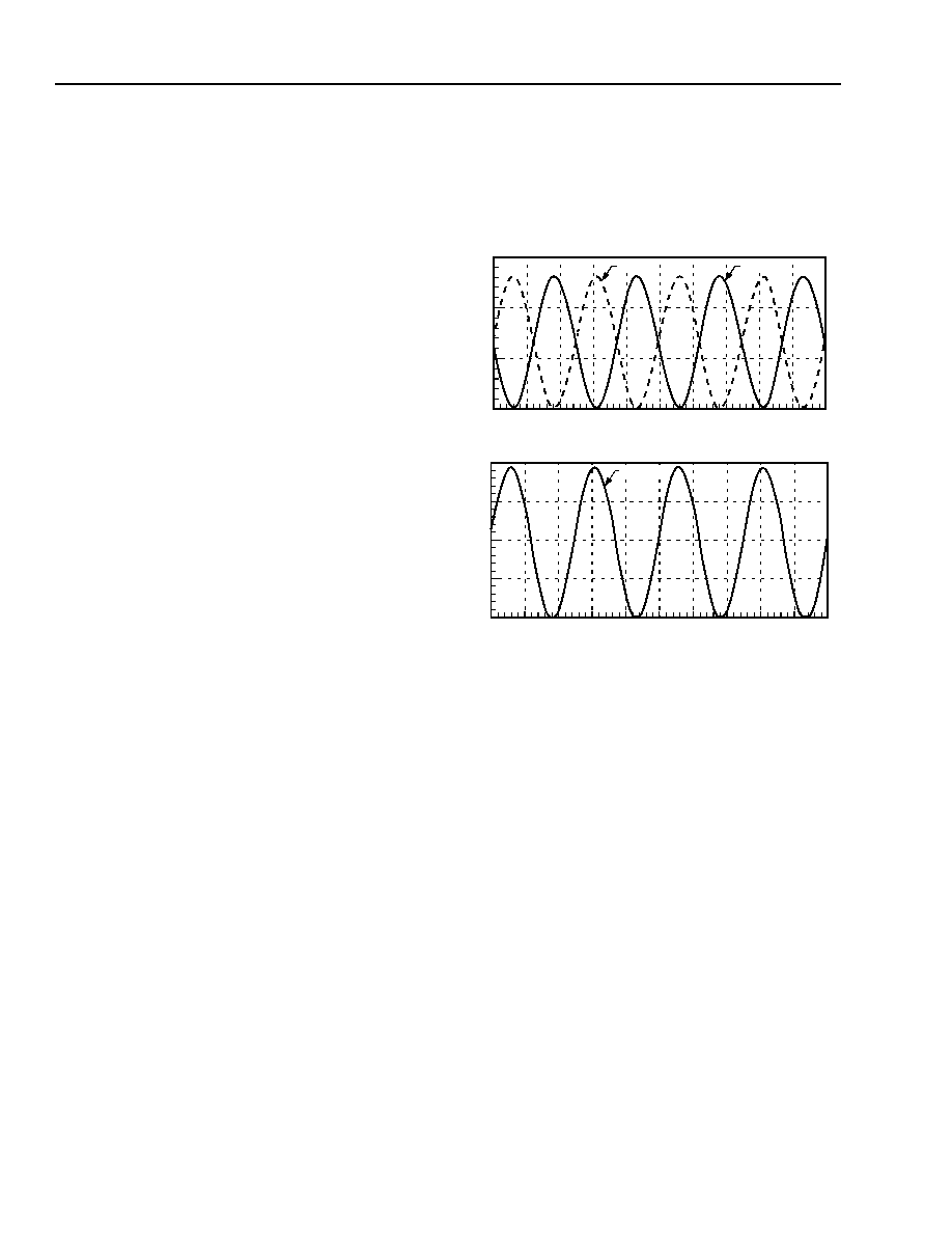
Data Sheet
September 2001
Short-Loop Sine Wave Ringing SLIC
L9215A/G
28
Agere Systems Inc.
Supervision
(continued)
Power Ring
(continued)
Sine Wave Input Signal and Sine Wave Power Ring
Signal Output
The low-voltage sine wave input is applied to the L9215
at pin RING
IN
. This signal should be ac-coupled
through 0.47
�
F. During the ring mode, the signal at
RING
IN
is amplified and presented to the subscriber
loop. The differential gain from RING
IN
to tip and ring is
a nominal 55.
When the device enters the ring mode, the tip/ring
overhead set at OVH and the scan clamp circuit is dis-
abled, allowing the voltage magnitude of the power ring
signal to be maximized. Additionally, in the ring mode,
the loop current limit is increased 2.5X the value set by
the V
PROG
voltage.
The magnitude of the power ring voltage will be a func-
tion of the gain of the ring amplifier, the high-voltage
battery, and the input signal at RING
IN
. The input range
of the signal at RING
IN
is 0 V to Vcc. As the input volt-
age at RING
IN
is increased, the magnitude of the power
ring voltage at tip and ring will increase linearly, per the
differential gain of 55, until the tip and ring drive amplifi-
ers begin to saturate. Once the tip and ring amplifiers
reach saturation, further increases of the input signal
will cause clipping distortion of the power ring signal at
tip and ring. The ring signal will appear balanced on tip
and ring. That is, the power ring signal is applied to
both tip and ring, with the signal on tip 180
�
out of
phase from the signal on ring.
Figure 11 shows typical operation of the ring mode,
prior to saturation of the tip and ring drive amplifiers. A
�70 V battery is used with a 100
loop and a 1 REN
load. The input signal is 1 V through a 0.47
�
F capaci-
tor at RING
IN
, (the input circuit is shown in Figure 12).
This produces a voltage swing from �34 V to �60 V on
ring and from �8 V to �34 V on tip, as shown in Figure
11. Thus, the total voltage swing is 52 V (60 V to 8 V)
for a 1 V input, which is approximately the differential
gain of the device. Note that the tip and ring power ring
signals will swing around V
BATTERY
divided by two. In
this case, there is a �70 V battery so tip and ring swing
around �34 V.
12-3573F
12-3574F
Figure 11. Ring Mode Typical Operation
0
�60
0.60
0.62
0.64
0.66
0.68
0.70
0.72
0.74
0.76
0.78
TIME
0.80
�20
�40
VRING
VTIP
1.0
�1.0
0.60
0.62
0.64
0.66
0.68
0.70
0.72
0.74
0.76
0.78
TIME
0.80
0.5
0.0
�0.5
VRINGIN
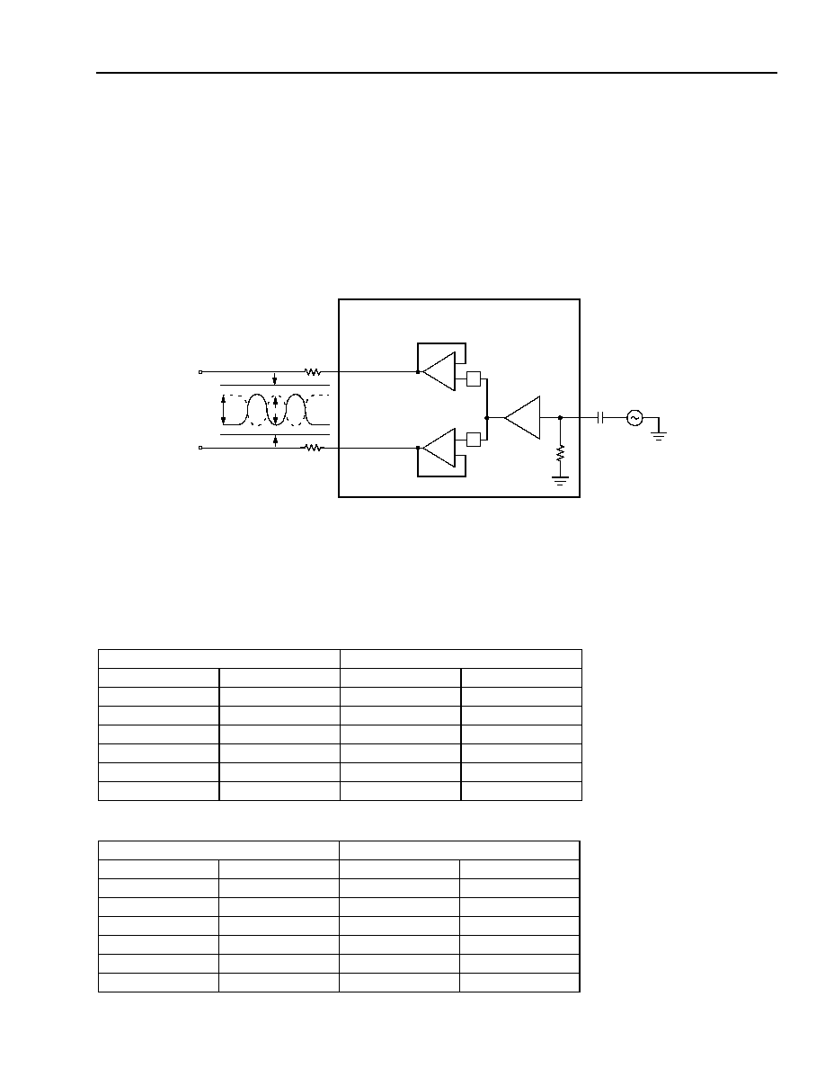
Data Sheet
September 2001
Short-Loop Sine Wave Ringing SLIC
L9215A/G
Agere Systems Inc.
29
Supervision
(continued)
Power Ring
(continued)
Sine Wave Input Signal and Sine Wave Power Ring Signal Output (continued)
It is recommended that the input level at RING
IN
be adjusted so that the power ring signal at tip and ring is just at
the edge or slightly clipping. This gives maximum power transfer with minimal distortion of the sine wave. The tip
side will saturate at a nominal 1 V above ground. The ring side will saturate at a nominal 3 V above battery. The
input circuit for a sine wave along with waveforms to illustrate the tip and ring saturation is shown in Figure 12.
12-3532.H(F)
Figure 12. RING
IN
Operation
The point at which clipping of the power ring signal begins at tip and ring is a function of the battery voltage, the
input capacitor at RING
IN
, and the input signal at RING
IN
and Vcc. Typical characteristic conditions showing the
onset of clipping are given below.
Table 21. Onset of Power Ringing Clipping V
CC
= 5 V, Cinput = 0.47
�
F
Table 22. Onset of Power Ringing Clipping V
CC
= 3.1 V, Cinput = 0.47
�
F
Input T/R
V
BAT1
(V)
Vrms (mV)
Vrms (V)
Gain
�70.15
891
46.88
52.62
�68.06
858
45.11
52.58
�66.00
833
43.69
52.45
�64.08
814
42.57
52.30
�62.04
789
41.21
52.23
�60.05
747
39.11
52.36
Input T/R
V
BAT1
(V)
Vrms (mV)
Vrms (V)
Gain
�70.12
894
47.15
52.74
�68.07
855
45.11
52.76
�66.06
824
43.38
52.65
�64.01
799
41.95
52.5
�62.00
780
40.79
52.29
�60.00
749
39.09
52.19
GND
V
BAT
PT
+1
TR
27.5x
RING
IN
0.47
�
F
INPUT
L9215
V
TIP
V
RING
�1
3 V
100 k
1 V
V
BAT
= �75 V
71 V
Data Sheet
September 2001
Short-Loop Sine Wave Ringing SLIC
L9215A/G
30
Agere Systems Inc.
Supervision
(continued)
Power Ring
(continued)
Sine Wave Input Signal and Sine Wave Power Ring Signal Output (continued)
During nonring modes, the sinusoidal ringing waveform may be left on at RING
IN
. Via the state table, the ring signal
will be removed from tip and ring even if the low-voltage input is still present at RING
IN
. There are certain timing
considerations that should be made with respect to state changes which are detailed in the
Switching Behavior of
L9215 Ringing SLIC
Application Note.
PWM Input Signal and Sine Wave Power Ring Signal Output
A pulse-width modulated (PWM) signal may be used to provide the ringing input to RING
IN
. The signal is applied
through a low-pass filter and ac-coupled into RING
IN
as shown below. This approach gives a sine wave output at
tip and ring.
12-3578bF
Figure 13. L9215/16 Ringing Input Circuit Selection Table for Square Wave and PWM Inputs
Table 23. Signal and Component Selection Chart
V
BAT
V
CC
Input
R1
C1
C2
CF
Typical 5 REN Ringing Voltage RMS
70 V
5 V
5 V Square
12 k
1
�
F
0.47
�
F
1.3
48 V
70 V
3 V
3 V Square
7 k
1
�
F
0.47
�
F
1.3
49 V
70 V
5 V
10 kHz PWM 5 V
10 k
0.22
�
F
0.47
�
F
sine
42 V
70 V
3 V
10 kHz PWM 3 V
10 k
0.22
�
F
0.47
�
F
sine
42 V
70 V
5 V
90 kHz PWM 5 V
7 k
0.1
�
F
0.47
�
F
sine
42 V
70 V
3 V
90 kHz PWM 3 V
7 k
0.1
�
F
0.47
�
F
sine
42 V
85 V
5 V
5 V Square
10 k
1
�
F
0.47
�
F
1.3
59 V
85 V
3 V
3 V Square
7 k
1
�
F
0.47
�
F
1.3
51 V
85 V
5 V
10 kHz PWM 5 V
10 k
0.22
�
F
0.47
�
F
sine
51 V
85 V
3 V
10 kHz PWM 3 V
4 k
0.22
�
F
0.47
�
F
sine
47 V
85 V
5 V
90 kHz PWM 5 V
4 k
0.1
�
F
0.47
�
F
sine
51 V
85 V
3 V
90 kHz PWM 3 V
4 k
0.1
�
F
0.47
�
F
sine
49 V
INPUT
R
1
C
1
C
2
RING
IN
L9215/16

Data Sheet
September 2001
Short-Loop Sine Wave Ringing SLIC
L9215A/G
Agere Systems Inc.
31
Supervision
(continued)
Power Ring
(continued)
PWM Input Signal and Sine Wave Power Ring Sig-
nal Output (continued)
Modulation waveforms showing PWM are in Figure 14
below.
Figure 14. Modulation Waveforms
5 V V
CC
Operation
A PWM signal was generated with an
HP
TM
8116
Function Generator modulated with a 20 Hz signal. The
optimal frequency used was 10 kHz. THE PWM signal
amplitude was 5.0 V (0 V to 5 V). This signal is shown
in Figure 15.
12-3575F
Figure 15. 5 V PWM Signal Amplitude
This input produced 44.96 Vrms ringing signal on
tip/ring under open loop conditions and 42.0 Vrms was
delivered to 5 REN load. The ringing output on ring,
with V
CC
= 5 V, is shown in Figure 16.
1660
Notes:
The modulating 20 Hz signal THD was measured at 1.3 %.
The tip/ring 20 Hz signal THD was measured at 1 %.
V
BAT1
= �70.6 V, V
BAT2
= �26.5 V, V
CC
= 5.019 V.
PWM input 10 kHz, 5.0 Vp-p.
R
1
= 10 k
, C
1
= 0.22
�
F, C
2
= 0.47
�
F.
Figure 16. Ringing Output on RING, with V
CC
= 5 V
12-3381(F)
A. Upper = Pwm Signal Centered at 10 kHz
Lower = Modulation Signal
12-3380(F)
B. Same as A but Expanded
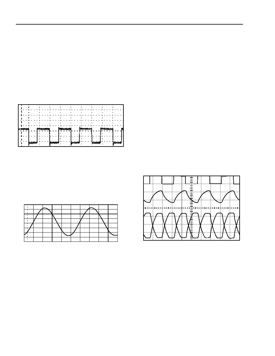
Data Sheet
September 2001
Short-Loop Sine Wave Ringing SLIC
L9215A/G
32
Agere Systems Inc.
Supervision
(continued)
Power Ring
(continued)
3.3 V V
CC
Operation
A PWM signal was generated with an
HP
8116 Func-
tion Generator modulated with a 20 Hz signal. The opti-
mal frequency used was 10 kHz. The PWM signal
amplitude was 3.10 V (0 V to 3.10 V). This input signal
is shown in Figure 17.
12-3571F
Figure 17. 3.3 V PWM Signal Amplitude
This produced 44.96 Vrms ringing signal on tip/ring
under open-loop conditions and 42.0 Vrms was deliv-
ered to 5 REN load. The ringing output on ring, with
V
CC
= 3.1 V is shown in Figure 18.
1660
Notes:
The modulating 20 Hz signal THD was measured at 1.3 %.
The tip/ring 20 Hz signal THD was measured at 1 %.
V
BAT1
= �70.6 V, V
BAT2
= �26.5 V, V
CC
= 3.10 V.
PWM input 10 kHz, 3.1 Vp-p.
R
1
= 10 k
, C
1
= 0.22
�
F, C
2
= 0.47
�
F.
Figure 18. Ringing Output on RING, with V
CC
= 3.1 V
During nonring modes, the PWM waveform may be left
on at RING
IN
. Via the state table, the ring signal will be
removed from tip and ring even if the low-voltage input
is still present at RING
IN
. There are certain timing con-
sideration that should be made with respect to state
changes which are detailed in the
Switching Behavior
of L9215 Ringing SLIC
Application Note.
Square Wave Input Signal and Trapezoidal Power
Ring Signal Output
A low-voltage square wave signal may be used to pro-
vide the ringing input to RING
IN
. The signal is applied
through a low-pass filter and ac-coupled into RING
IN
as
shown in Figure 13 and Table 23. This approach gives
a trapezoidal wave output at tip and ring.
Using this approach, a trapezoidal waveform can be
achieved at tip and ring. This has the advantage of
increasing the power transfer to the load for a given
battery voltage, thus increasing the effective ringing
loop length as compared to a sine wave. The actual
crest factor achieved is a function of the magnitude of
the battery, the magnitude of the input voltage, fre-
quency, and R
1
.
12-3572F
Notes:
CH1 = CMOS Input (5 V) at RING
IN
.
CH2 = Filtered input at RING
IN
.
CH3 = Tip.
CH4 = Ring.
R
1
= 14 k
, C
1
= 1.0
�
F, C
2
= 0.47
�
F.
V
BAT1
= �70 V, Vrms
= 51 V, V
p-p
= 67 V, frequency = 20 Hz, crest
factor = 1.3.
Figure 19. Square Wave Input Signal and Trapezoi-
dal Power Ring Signal Output
CH1
CH2
CH3
CH4
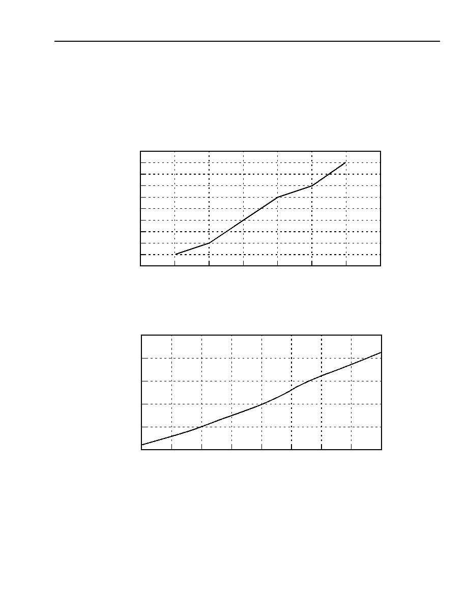
Data Sheet
September 2001
Short-Loop Sine Wave Ringing SLIC
L9215A/G
Agere Systems Inc.
33
Supervision
(continued)
Power Ring
(continued)
Square Wave Input Signal and Trapezoidal Power Ring Signal Output (continued)
The following charts are meant to give some guidance to the relationship between crest factor, battery voltage, and
R
1
value.
12-3576F
Figure 20. Crest Factor vs. Battery Voltage
12-3577F
Figure 21. Crest Factor vs. R (k
)
During nonring modes, the square wave input may be left on or removed from RING
IN
. Via the state table, the ring
signal will be removed from tip and ring even if the low-voltage input is still present at RING
IN
. However, removing
the waveform has certain advantages in terms of the timing of state. These advantages are detailed in the
Switch-
ing Behavior of L9215 Ringing SLIC
Application Note.
1.36
58
BAT V
CF
60
62
64
66
68
70
72
1.35
1.34
1.33
1.32
1.31
1.3
1.29
1.28
1.27
1.26
1.5
1.45
10
R (k
)
CF
1.4
1.35
1.3
1.25
10.5
11
11.5
12
12.5
13
13.5
14

Data Sheet
September 2001
Short-Loop Sine Wave Ringing SLIC
L9215A/G
34
Agere Systems Inc.
Periodic Pulse Metering (PPM)
Periodic pulse metering (PPM), also referred to as tele-
tax (TTX), is input to the PPM
IN
input of the L9215.
Upon application of appropriate logic control, this sig-
nal is presented to the tip/ring subscriber loop. The
state of the L9215 should be changed while applying
PPM signals during the quiet interval of the PPM
cadence. The L9215 assumes that a shaped PPM sig-
nal is applied to the PPM
IN
input.
PPM input signals may be a maximum 1.25 V at
PPM
IN
. The gain from PPM
IN
to tip/ring is 6 dB. Thus,
for 1.0 Vrms at tip and ring, apply a 0.50 Vrms signal at
PPM
IN
. The PPM signal should be ac coupled to
PPM
IN
through a 10 nF capacitor.
When applied to tip and ring, the PPM signal will also
be returned through the SLIC and will appear at the
SLIC VITR output. The concern is that this high-voltage
signal can overload an internal SLIC amplifier or the
codec input and cause distortion of the (desired) ac
signal. Because the L9215 is intended for short dc
loops, the assumption is that low meter pulse signals
are sufficient. The maximum allowed PPM current at
the 200
ac meter pulse load to avoid saturation of the
device's internal AAC amplifier is 3 mArms. This signal
level is sufficient to provide a minimum 200 mVrms to
the 200
PPM load under maximum specified dc loop
conditions. Above 3 mArms PPM current, external
meter pulse rejection may be required. If on-hook
transmission of PPM is required, sufficient overhead to
accommodate on-hook transmission must be pro-
grammed by the user at the OVH input.
ac Applications
ac Parameters
There are four key ac design parameters. Termination
impedance is the impedance looking into the 2-wire
port of the line card. It is set to match the impedance of
the telephone loop in order to minimize echo return to
the telephone set. Transmit gain is measured from the
2-wire port to the PCM highway, while receive gain is
done from the PCM highway to the transmit port.
Transmit and receive gains may be specified in terms
of an actual gain, or in terms of a transmission level
point (TLP), that is the actual ac transmission level in
dBm. Finally, the hybrid balance network cancels the
unwanted amount of the receive signal that appears at
the transmit port.
Codec Types
At this point in the design, the codec needs to be
selected. The interface network between the SLIC and
codec can then be designed. Below is a brief codec
feature summary.
First-Generation Codecs
These perform the basic filtering, A/D (transmit), D/A
(receive), and
�
-law/A-law companding. They all have
an op amp in front of the A/D converter for transmit
gain setting and hybrid balance (cancellation at the
summing node). Depending on the type, some have
differential analog input stages, differential analog out-
put stages, 5 V only or
�
5 V operation, and
�
-law/A-law
selectability. These are available in single and quad
designs. This type of codec requires continuous time
analog filtering via external resistor/capacitor networks
to set the ac design parameters. An example of this
type of codec is the Agere T7504 quad 5 V only codec.
This type of codec tends to be the most economical in
terms of piece part price, but tends to require more
external components than a third-generation codec.
Further ac parameters are fixed by the external R/C
network so software control of ac parameters is diffi-
cult.
Third-Generation Codecs
This class of devices includes all ac parameters set
digitally under microprocessor control. Depending on
the device, it may or may not have data control latches.
Additional functionality sometimes offered includes
tone plant generation and reception, PPM generation,
test algorithms, and echo cancellation. Again, this type
of codec may be 3.3 V, 5 V only, or
�
5 V operation, sin-
gle quad or 16 channel, and
�
-law/A-law or 16-bit linear
coding selectable. Examples of this type of codec are
the Agere T8535/6 (5 V only, quad, standard features),
T8537/8 (3.3 V only, quad, standard features), T8533/4
(5 V only, quad with echo cancellation), and the
T8531/32 (5 V only 16 channel).
ac Interface Network
The ac interface network between the L9215 and the
codec will vary depending on the codec selected. With
a first-generation codec, the interface between the
L9215 and codec actually sets the ac parameters. With
a third-generation codec, all ac parameters are set dig-
itally, internal to the codec; thus, the interface between

Data Sheet
September 2001
Short-Loop Sine Wave Ringing SLIC
L9215A/G
Agere Systems Inc.
35
ac Applications
(continued)
ac Interface Network
(continued)
the L9215 and this type of codec is designed to avoid
overload at the codec input in the transmit direction
and to optimize signal to noise ratio (S/N) in the receive
direction.
Because the design requirements are very different
with a first- or third-generation codec, the L9215 is
offered with two different receive gains. Each receive
gain was chosen to optimize, in terms of external com-
ponents required, the ac interface between the L9215
and codec.
With a first-generation codec, the termination imped-
ance is set by providing gain shaping through a feed-
back network from the SLIC VITR output to the SLIC
RCVN/RCVP inputs. The L9215 provides a transcon-
ductance from T/R to VITR in the transmit direction and
a single-ended to differential gain from either RCVN or
RCVP to T/R in the receive direction. Assuming a short
from VITR to RCVN or RCVP, the maximum imped-
ance that is seen looking into the SLIC is the product of
the SLIC transconductance times the SLIC receive
gain, plus the protection resistors. The various speci-
fied termination impedance can range over the voice-
band as low as 300
up to over 1000
. Thus, if the
SLIC gains are too low, it will be impossible to synthe-
size the higher termination impedances. Further, the
termination that is achieved will be far less than what is
calculated by assuming a short for SLIC output to SLIC
input. In the receive direction, in order to control echo,
the gain is typically a loss, which requires a loss net-
work at the SLIC RCVN/RCVP inputs, which will
reduce the amount of gain that is available for termina-
tion impedance. For this reason, a high-gain SLIC is
required with a first-generation codec.
With a third-generation codec, the line card designer
has different concerns. To design the ac interface, the
designer must first decide upon all termination imped-
ance, hybrid balances, and transmission-level point
(TLP) requirements that the line card must meet. In the
transmit direction, the only concern is that the SLIC
does not provide a signal that is too hot and overloads
the codec input. Thus, for the highest TLP that is being
designed to, given the SLIC gain, the designer, as a
function of voiceband frequency, must ensure the
codec is not overloaded. With a given TLP and a given
SLIC gain, if the signal will cause a codec overload, the
designer must insert some sort of loss, typically a resis-
tor divider, between the SLIC output and codec input.
Note also that some third-generation codecs require
the designer to provide an inherent resistive termina-
tion via external networks. The codec will then provide
gain shaping, as a function of frequency, to meet the
return loss requirements. This feedback will increase
the signal at the codec input and increase the likeli-
hood that a resistor divider is needed in the transmit
direction. Further stability issues may add external
components or excessive ground plane requirements
to the design.
In the receive direction, the issue is to optimize the
S/N. Again, the designer must consider all the consid-
ered TLPs. The idea is, for all desired TLPs, to run the
codec at or as close as possible to its maximum output
signal, to optimize the S/N. Remember, noise floor is
constant, so the hotter the signal from the codec, the
better the S/N. The problem is if the codec is feeding a
high-gain SLIC, either an external resistor divider is
needed to knock the gain down to meet the TLP
requirements, or the codec is not operated near maxi-
mum signal levels, thus compromising the S/N.
Thus, it appears that the solution is to have a SLIC with
a low gain, especially in the receive direction. This will
allow the codec to operate near its maximum output
signal (to optimize S/N), without an external resistor
divider (to minimize cost).
To meet the unique requirements of both type of
codecs, the L9215 offers two receive gain choices.
These receive gains are mask-programmable at the
factory and are offered as two different code variations.
For interface with a first-generation codec, the L9215 is
offered with a receive gain of 8. For interface with a
third-generation codec, the L9215 is offered with a
receive gain of 2. In either case, the transconductance
in the transmit direction or the transmit gain is 300
.
This selection of receive gain gives the designer the
flexibility to maximize performance and minimize exter-
nal components, regardless of the type of codec cho-
sen.
Design Examples
First-Generation Codec ac Interface Network--
Resistive Termination
The following reference circuit shows the complete
SLIC schematic for interface to the Agere T7504 first-
generation codec for a resistive termination imped-
ance. For this example, the ac interface was designed
for a 600
resistive termination and hybrid balance
with transmit gain and receive gain set to 0 dBm. For
illustration purposes, no PPM injection was assumed in
this example. This implies use of the default overhead
voltage and no components for meter pulse rejection.
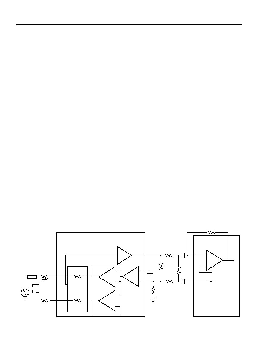
Data Sheet
September 2001
Short-Loop Sine Wave Ringing SLIC
L9215A/G
36
Agere Systems Inc.
ac Applications
(continued)
Design Examples
(continued)
First-Generation Codec ac Interface Network--
Resistive Termination (continued)
This is a lower feature application example and uses
single battery operation, fixed overhead, current limit,
and loop closure threshold.
Resistor R
GN
is optional. It compensates for any mis-
match of input bias voltage at the RCVN/RCVP inputs.
If it is not used, there may be a slight offset at tip and
ring due to mismatch of input bias voltage at the
RCVN/RCVP inputs. It is very common to simply tie
RCVN directly to ground in this particular mode of oper-
ation. If used, to calculate RGN, the impedance from
RCVN to ac ground should equal the impedance from
RCVP to ac ground.
Example 1, Real Termination
The following design equations refer to the circuit in
Figure 22. Use these to synthesize real termination
impedance.
Termination Impedance:
z
T
=
Receive Gain:
Transmit Gain:
Hybrid Balance:
h
bal
= 20log
h
bal
= 20log
To optimize the hybrid balance, the sum of the currents
at the VFX input of the codec op amp should be set to
0. The expression for ZHB becomes the following:
V
T/R
I
T/R
�
------------
z
T
50
2
+
R
P
2400
1
R
T 1
R
G P
---------
R
T 1
R
R CV
------------
+
+
-----------------------------------
+
=
g
rcv
V
T/R
V
FR
------------
=
g
rcv
8
1
R
R CV
R
T 1
-----------
R
R C V
R
G P
------------
+
+
1
Z
T
Z
T/R
---------
+
------------------------------------------------------------------
=
g
tx
V
GSX
V
T/R
-----------
=
g
t x
R
X
�
R
T 2
---------
300
Z
T/R
---------
�
=
R
X
R
HB
------------
g
tx
�
g
rcv
�
V
GSX
V
F R
---------------
R
H B
k
( )
R
X
g
tx
g
rcv
�
-------------------
=
12-2554.V (F)
Figure 22. ac Equivalent Circuit
R
P
Z
T
+
�
R
P
V
T/R
I
T/R
V
S
Z
T/R
+
�
RING
A
V
= �1
A
V
= 1
VITR
CURRENT
SENSE
TIP
+
�
R
T1
R
RCV
R
HB1
R
T2
RCVN
RCVP
R
X
VGSX
VF
X
IN
V
FR
1/4 T7504 CODEC
R
GP
+2.4 V
�0.300 V/mA
A
V
= 4
L9215
VF
X
IP
18
18
+
�
+
�
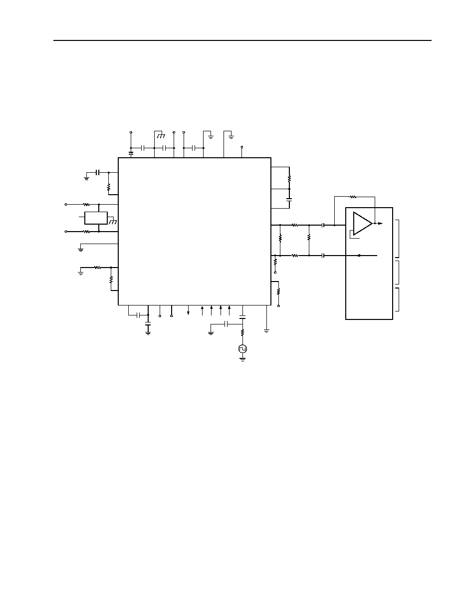
Data Sheet
September 2001
Short-Loop Sine Wave Ringing SLIC
L9215A/G
Agere Systems Inc.
37
ac Applications
(continued)
Design Examples
(continued)
Example 1, Real Termination (continued)
Figure 23. Agere T7504 First-Generation Codec Resistive Termination; Nonmeter Pulse Application
V
BAT1
BGND V
BAT2
V
CC
AGND
ICM
TRGDET
ground key
not used
C
BAT1
0.1
�
F
C
BAT2
0.1
�
F
C
CC
0.1
�
F
RTFLT
DCOUT
PR
PT
V
REF
C
RT
0.1
�
F
R
RT
383 k
AGERE
L7591
V
BAT1
FUSIBLE OR PTC
30
30
R
VREF
80.6 k
CF1
CF2
rate of battery
reversal not
ramped
FB1 FB2 NSTAT BR B2 B1 B0
C
F1
0.22
�
F
C
F2
0.1
�
F
RING
IN
PPM
IN
VITR
RCVP
RCVN
ITR
VTX
TXI
R
GX
4750
V
BAT1
D
BAT1
V
BAT2
V
CC
C
TX
0.1
�
F
C
2
0.47
�
F
not
used
1/4 T7504
CODEC
R
T6
C
C1
R
X
GSX
+2.4 V
R
HB1
VFXIN
R
RCV
R
T3
R
GP
C
C2
V
FRO
DX
DR
FSE
FSEP
MCLK
ASEL
CONTROL
INPUTS
SYNC
AND
PCM
HIGHWAY
CLOCK
R
N2
�
+
49.9 k
100 k
100 k
60.4 k
0.1
�
F
17.65 k
26.7 k
69.8 k
0.1 �F
L9215A
V
PROG
(I
LIMIT
= 25 mA)
23.7 k
R
VPROG
FUSIBLE OR PTC
OVH (DEFAULT OVERHEAD)
V
REF
V
REF
R
1
12 k
C
1
1.0
�
F

Data Sheet
September 2001
Short-Loop Sine Wave Ringing SLIC
L9215A/G
38
Agere Systems Inc.
ac Applications
(continued)
Design Examples
(continued)
Example 1, Real Termination (continued)
Table 24. Parts List L9215; Agere T7504 First-Generation Codec Resistive Termination; Nonmeter Pulse
Application
Notes:
Termination impedance = 600
.
Hybrid balance = 600
.
T x = 0 dBm Rx = 0 dBm.
Name
Value
Tolerance
Rating
Function
Fault Protection
R
PT
30
1%
Fusible or PTC Protection resistor.
R
PR
30
1%
Fusible or PTC Protection resistor.
Protector
Agere L7591
--
--
Secondary protection.
Power Supply
C
BAT1
0.1
�
F
20%
100 V
V
BAT
filter capacitor.
C
BAT2
0.1
�
F
20%
50 V
V
BAT
filter capacitor. |V
BAT2
| < |V
BAT1
|.
D
BAT1
1N4004
--
--
Reverse current.
C
CC
0.1
�
F
20%
10 V
V
CC
filter capacitor.
C
F1
0.22
�
F
20%
100 V
Filter capacitor.
C
F2
0.1
�
F
20%
100 V
Filter capacitor.
dc Profile
R
VPROG
23.7 k
1%
1/16 W
With R
VREF
fixes dc current limit.
R
VREF
80.6 k
1%
1/16 W
With R
VPROG
fixes dc current limit.
Ring/Ring Trip
C
1
1.0
�
F
20%
10 V
Ring filter for square wave.
C
2
0.47
�
F
20%
10 V
ac-couple input ring signal.
R
1
12 k
1%
1/16 W
Ring filter for square wave.
C
RT
0.1
�
F
20%
10 V
Ring trip filter capacitor.
R
RT
383 k
1%
1/16 W
Ring trip filter resistor.
ac Interface
R
GX
4750
1%
1/16 W
Sets T/R to VITR transconductance.
C
TX
0.1
�
F
20%
10 V
ac/dc separation.
C
C1
0.1
�
F
20%
10 V
dc blocking capacitor.
C
C2
0.1
�
F
20%
10 V
dc blocking capacitor.
R
T3
69.8 k
1%
1/16 W
With R
GP
and R
RCV
, sets termination
impedance and receive gain.
R
T6
49.9 k
1%
1/16 W
With R
X
, sets transmit gain.
R
X
100 k
1%
1/16 W
With R
T6
, sets transmit gain.
R
HB1
100 k
1%
1/16 W
With R
X
, sets hybrid balance.
R
RCV
60.4 k
1%
1/16 W
With R
GP
and R
T3
, sets termination
impedance and receive gain.
R
GP
26.7 k
1%
1/16 W
With R
RCV
and R
T3
, sets termination
impedance and receive gain.
R
GN
Optional
17.6 k
1%
1/16 W
Optional. Compensates for input off-
set at RCVN/RCVP.
Data Sheet
September 2001
Short-Loop Sine Wave Ringing SLIC
L9215A/G
Agere Systems Inc.
39
ac Applications
(continued)
Design Examples
(continued)
First-Generation Codec ac Interface Network--
Complex Termination
The following reference circuit shows the complete
SLIC schematic for interface to the Agere T7504 first-
generation codec for the German complex termination
impedance. For this example, the ac interface was
designed for a 220
+ (820
|| 115 nF) complex ter-
mination and hybrid balance with transmit gain and
receive gain set to 0 dBm. For illustration purposes,
1 Vrms PPM injection was assumed in this example.
This implies the overhead voltage is increased to
7.24 V and no meter pulse rejection is required. Also,
this example illustrates the device using fixed overhead
and current limit.
Complex Termination Impedance Design Example
The gain shaping necessary for a complex termination
impedance may be done by shaping across the AX
amplifier at nodes ITR and VTX.
Complex termination is specified in the form:
5-6396(F)
To work with this application, convert termination to the
form:
5-6398(F)
where:
R
1
� = R
1
+ R
2
R
2
� =
(R
1
+ R
2
)
C� =
C
ac Interface Using First-Generation Codec
R
GX
/R
TGS
/C
GS
(Z
TG
): these components give gain shap-
ing to get good gain flatness. These components are a
scaled version of the specified complex termination
impedance.
Note for pure (600
) resistive terminations, compo-
nents R
TGS
and C
GS
are not used. Resistor R
GX
is used
and is still 4750
.
R
X
/R
T6
: with other components set, the transmit gain
(for complex and resistive terminations) R
X
and R
T6
are
varied to give specified transmit gain.
R
T3
/R
RCV
/R
GP
: for both complex and resistive termina-
tions, the ratio of these resistors sets the receive gain.
For resistive terminations, the ratio of these resistors
sets the return loss characteristic. For complex termi-
nations, the ratio of these resistors sets the low-fre-
quency return loss characteristic.
C
N
/R
N1
/R
N2
: for complex terminations, these compo-
nents provide high-frequency compensation to the
return loss characteristic.
For resistive terminations, these components are not
used and RCVN is connected to ground via a resistor.
R
HB
: sets hybrid balance for all terminations.
Set Z
TG
--Gain Shaping
Z
TG
= R
GX
|| R
TGS
+ C
GS
which is a scaled version of
Z
T/R
(the specified termination resistance) in the
R
1
� || R
2
� + C� form.
R
GX
must be 4750
to set SLIC transconductance to
300 V/A.
R
GX
= 4750
At dc, C
GS
and C� are open.
R
GX
= M x R
1
�
where M is the scale factor.
M =
It can be shown:
R
TGS
= M x R
2
�
and
C
TGS
=
R
2
C
R
1
R
1
�
C�
R
2
�
R
1
R
2
-------
R
2
R
1
R
2
+
---------------------
2
4750
R
1
--------------
C
M
------
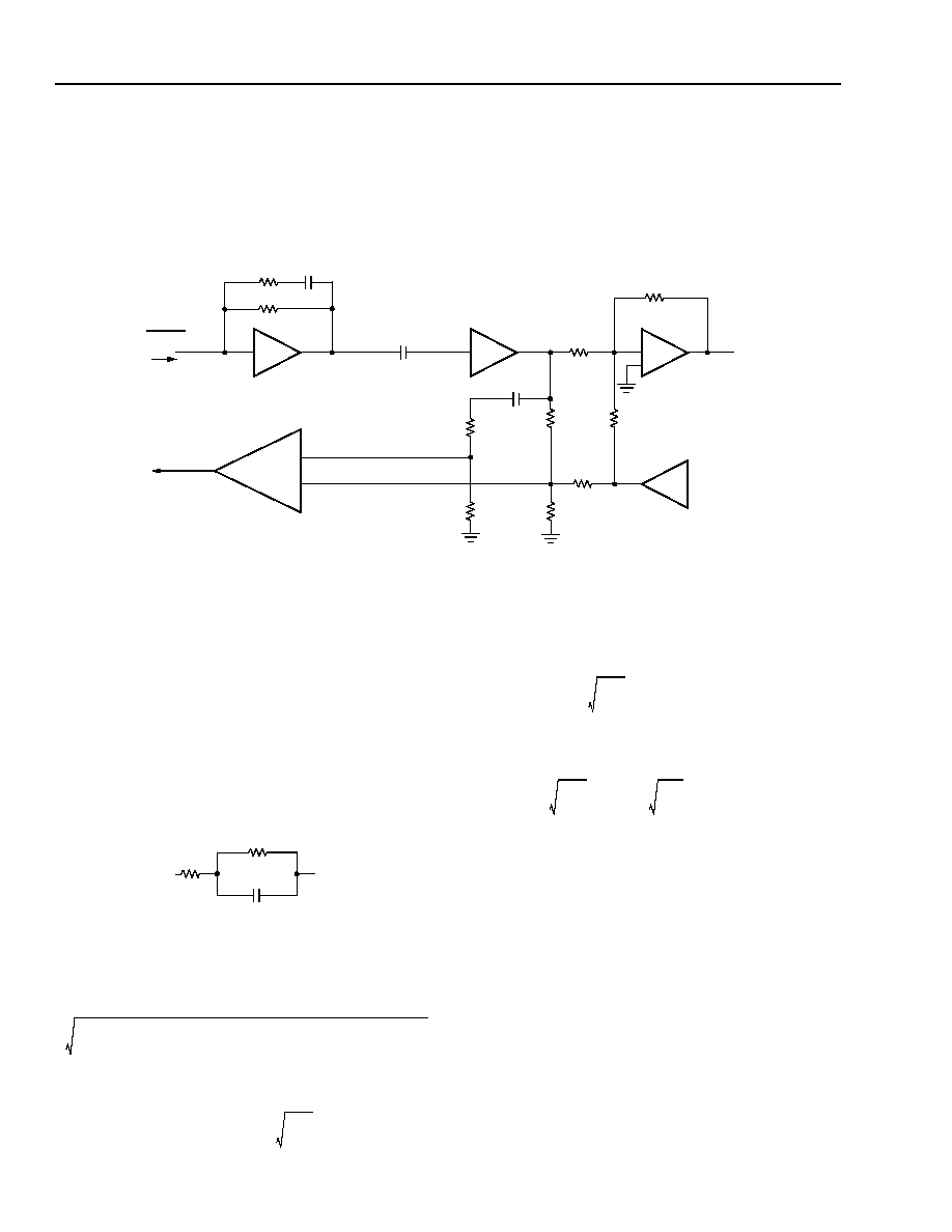
Data Sheet
September 2001
Short-Loop Sine Wave Ringing SLIC
L9215A/G
40
Agere Systems Inc.
ac Applications
(continued)
Design Examples
(continued)
Set Z
TG
--Gain Shaping (continued)
5-6400.P (F)
Figure 24. Interface Circuit Using First-Generation Codec (Blocking Capacitors Not Shown)
0.1
�
F
R
TGS
V
TX
R
GX
= 4750
T
XI
V
ITR
R
T6
R
x
R
T3
R
HB
CODEC
OUTPUT
DRIVE
AMP
CODEC
OP AMP
�
+
20
C
N
R
N1
R
N2
R
GP
R
RCV
�I
T/R
318.25
C
GS
RCVN
RCVP
Transmit Gain
Transmit gain will be specified as a gain from T/R to
PCM, T
X
(dB). Since PCM is referenced to 600
and
assumed to be 0 dB, and in the case of T/R being refer-
enced to some complex impedance other than 600
resistive, the effects of the impedance transformation
must be taken into account.
Again, specified complex termination impedance at T/R
is of the form:
5-6396(F)
First, calculate the equivalent resistance of this network
at the midband frequency of 1000 Hz.
R
EQ
=
Using R
EQ
, calculate the desired transmit gain, taking
into account the impedance transformation:
T
X
(dB) = T
X (specified[dB])
+ 20log
T
X (specified[dB])
is the specified transmit gain. 600
is the
impedance at the PCM, and R
EQ
is the impedance at
tip and ring. 20log
represents the power
loss/gain due to the impedance transformation.
Note in the case of a 600
pure resistive termination
at T/R 20log
= 20log
= 0.
Thus, there is no power loss/gain due to impedance
transformation and T
X
(dB) = T
X (specified[dB])
.
Finally, convert T
X
(dB) to a ratio, g
TX
:
T
X
(dB) = 20log g
TX
The ratio of R
X
/R
T6
is used to set the transmit gain:
= g
TX
�
�
with a quad Agere codec
such as T7504:
R
X
< 200 k
R
2
C
R
1
2
f
(
)
2
C
12
R
1
R
22
R
1
R
2
+
+
1
2
f
(
)
2
R
22
C
12
+
-----------------------------------------------------------------------------
2
2
f
R
22
C
1
1
2
f
(
)
2
R
22
C
12
+
---------------------------------------------------
2
+
600
R
EQ
-----------
600
R
EQ
-----------
600
R
EQ
-----------
600
600
----------
R
X
R
T6
----------
318.25
20
------------------
1
M
-----

Data Sheet
September 2001
Short-Loop Sine Wave Ringing SLIC
L9215A/G
Agere Systems Inc.
41
ac Applications
(continued)
Design Examples
(continued)
Receive Gain
Ratios of R
RCV
, R
T3
, and R
GP
will set both the low-fre-
quency termination and receive gain for the complex
case. In the complex case, additional high-frequency
compensation, via C
N
, R
N1
, and R
N2
, is needed for the
return loss characteristic. For resistive termination, C
N
,
R
N1
, and R
N2
are not used and RCVN is tied to ground
via a resistor.
Determine the receive gain, g
RCV
, taking into account
the impedance transformation in a manner similar to
transmit gain.
R
X
(dB) = R
X (specified[dB])
+ 20log
R
X
(dB) = 20log g
RCV
Then:
g
RCV
=
and low-frequency termination
Z
TER(low)
=
+ 2R
P
+ 50
Z
TER(low)
is the specified termination impedance assum-
ing low frequency (C or C� is open).
R
P
is the series protection resistor.
50
is the typical internal feed resistance.
These two equations are best solved using a computer
spreadsheet.
Next, solve for the high-frequency return loss compen-
sation circuit, C
N
, R
N1
, and R
N2
:
C
N
R
N2
=
C
G
R
TGP
R
N1
= R
N2
There is an input offset voltage associated with nodes
RCVN and RCVP. To minimize the effect of mismatch
of this voltage at T/R, the equivalent resistance to ac
ground at RCVN should be approximately equal to that
at RCVP. Refer to Figure 25 (with dc blocking capaci-
tors). To meet this requirement, R
N2
= R
GP
|| R
T3
.
Hybrid Balance
Set the hybrid cancellation via R
HB
.
R
HB
=
If a 5 V only codec such as the Agere T7504 is used,
dc blocking capacitors must be added as shown in
Figure 25. This is because the codec is referenced to
2.5 V and the SLIC to ground--with the ac coupling, a
dc bias at T/R is eliminated and power associated with
this bias is not consumed.
Typically, values of 0.1 �F to 0.47 �F capacitors are
used for dc blocking. The addition of blocking capaci-
tors will cause a shift in the return loss and hybrid bal-
ance frequency response toward higher frequencies,
degrading the lower-frequency response. The lower
the value of the blocking capacitor, the more pro-
nounced the effect is, but the cost of the capacitor is
lower. It may be necessary to scale resistor values
higher to compensate for the low-frequency response.
This effect is best evaluated via simulation. A
PSPICE
�
model for the L9215 is available.
Design equation calculations seldom yield standard
component values. Conversion from the calculated
value to standard value may have an effect on the ac
parameters. This effect should be evaluated and opti-
mized via simulation.
R
EQ
600
-----------
4
1
R
RCV
R
T3
---------------
R
RCV
R
GP
---------------
+
+
------------------------------------------------
2400
1
R
T3
R
GP
------------
R
T3
R
RCV
---------------
+
+
--------------------------------------------
2R
P
2400
-------------
2400
2R
P
-------------
R
T GS
R
T GP
--------------
1
�
R
X
g
RCV
g
TX
�
-------------------------------
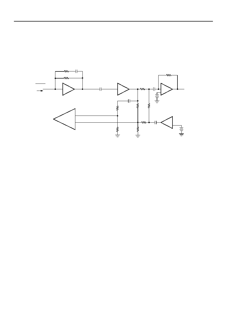
Data Sheet
September 2001
Short-Loop Sine Wave Ringing SLIC
L9215A/G
42
Agere Systems Inc.
ac Applications
(continued)
Design Examples
(continued)
Blocking Capacitors
5-6401.M (F)
Figure 25. ac Interface Using First-Generation Codec (Including Blocking Capacitors) for Complex Termi-
nation Impedance
0.1
�
F
R
TGS
VTX
R
GX
= 4750
TXI
VITR
R
T6
R
x
R
T3
R
HB
CODEC
OUTPUT
DRIVE
AMP
CODEC
OP AMP
�
+
20
C
N
R
N1
R
N2
R
GP
R
RCV
�I
T/R
318.25
C
GS
C
B1
2.5 V
C
B2
RCVN
RCVP

Data Sheet
September 2001
Short-Loop Sine Wave Ringing SLIC
L9215A/G
Agere Systems Inc.
43
ac Applications
(continued)
Design Examples
(continued)
Blocking Capacitors (continued)
Figure 26. Agere T7504 First-Generation Codec Complex Termination; Meter Pulse Application
V
BAT1
BGND
V
BAT2
V
CC
AGND
ICM
TRGDET
ground key
not used
C
BAT1
0.1
�
F
C
BAT2
0.1
�
F
C
CC
0.1
�
F
RTFLT
DCOUT
PR
PT
C
RT
0.1
�
F
R
RT
383 k
AGERE
L7591
V
BAT1
FUSIBLE
30
rate of battery
reversal not
ramped
PPM
0.5 V
RMS
C
PPM
10 nF
VITR
RCVP
RCVN
ITR
VTX
TXI
R
GX
4750
R
TGS
1.74 k
C
GS
12 nF
V
BAT1
D
BAT1
V
BAT2
V
CC
C
TX
0.1
�
F
1/4 T7504
CODEC
R
T6
R
X
GSX
+2.4 V
R
HB1
VFXIN
R
T3
R
RCV
C
N
R
GP
VFRO
DX
DR
FSE
FSEP
MCLK
ASEL
CONTRO
INPUTS
SYNC
AND
PCM
HIGHWAY
CLOCK
R
N2
�
+
30
C
C2
L9215A
C
C1
CF1
CF2 FB1 FB2 NSTAT BR B2 B1 B0
C
F1
0.22
�
F
C
F2
0.1
�
F
RING
IN
PPM
IN
C
RING
0.47
�
F
FROM/TO CONTROL
RING
FUSIBLE
47.5 k
54.9 k
127
R
N1
k
59.0 k
49.9 k
113 k
120 pF
0.1
�
F
0.1
�
F
40.6 k
OVH
V
PROG
(I
LIMIT
= 25 mA)
V
REF
R
OVH
10 k
R
VREF
80.6 k
R
VPROG
20 k
OR PTC
OR PTC
V
REF
V
REF
115 k

Data Sheet
September 2001
Short-Loop Sine Wave Ringing SLIC
L9215A/G
44
Agere Systems Inc.
Applications
(continued)
Design Examples
(continued)
Blocking Capacitors (continued)
Table 25. Parts List L9215; Agere T7504 First-Generation Codec Complex Termination; Meter Pulse
Application
Termination impedance = 220
+ (820
|| 115 nF), hybrid balance = 220
+ (820
|| 115 nF) Tx = 0 dBm,
Rx = 0 dBm.
Name
Value
Tolerance
Rating
Function
Fault Protection
R
PT
30
1%
Fusible or PTC Protection resistor.
R
PR
30
1%
Fusible or PTC Protection resistor.
Protector
Agere
L7591
--
--
Secondary protection.
Power Supply
C
BAT1
0.1
�
F
20%
100 V
V
BAT
filter capacitor.
C
BAT2
0.1
�
F
20%
50 V
V
BAT
filter capacitor. |V
BAT2
| < |V
BAT1
|.
D
BAT1
1N4004
--
--
Reverse current.
C
CC
0.1
�
F
20%
10 V
V
CC
filter capacitor.
C
F1
0.22
�
F
20%
100 V
Filter capacitor.
C
F2
0.1
�
F
20%
100 V
Filter capacitor.
dc Profile
R
VPROG
20 k
1%
1/16 W
With R
VREF
fixes dc current limit.
R
VOVH
10 k
1%
1/16 W
With R
VREF
fixes overhead voltage.
R
VREF
80.6 k
1%
1/16 W
With R
VPROG
fixes dc current limit/overhead.
Ring/Ring Trip
C
RING
0.47
�
F
20%
10 V
ac-couple input ring signal.
C
RT
0.1
�
F
20%
10 V
Ring trip filter capacitor.
R
RT
383 k
1%
1/16 W
Ring trip filter resistor.
PPM
C
PPM
10 nF
20%
10 V
ac-couple PPM input.
ac Interface
R
GX
4750
1%
1/16 W
Sets T/R to VITR transconductance.
R
TGS
1.74 k
1%
1/16 W
Gain shaping for complex termination.
C
GS
12 nF
5%
10 V
Gain shaping for complex termination.
C
TX
0.1
�
F
20%
10 V
ac/dc separation.
C
C1
0.1
�
F
20%
10 V
dc blocking capacitor.
C
C2
0.1
�
F
20%
10 V
dc blocking capacitor.
R
T3
49.9 k
1%
1/16 W
With R
GP
and R
RCV
, sets termination impedance and receive
gain.
R
T6
40.2 k
1%
1/16 W
With R
X
, sets transmit gain.
R
X
115 k
1%
1/16 W
With R
T6
, sets transmit gain.
R
HB1
113 k
1%
1/16 W
With R
X
, sets hybrid balance.
R
RCV
59.0 k
1%
1/16 W
With R
GP
and R
T3
, sets termination impedance and receive gain.
R
GP
54.9 k
1%
1/16 W
With R
RCV
and R
T3
, sets termination impedance and receive
gain.
C
N
120 pF
20%
10 V
High frequency compensation.
R
N1
127 k
1%
1/16 W
High frequency compensation.
R
N2
47.5 k
1%
1/16 W
High frequency compensation, compensate for dc offset at
RCVP/RCVN.
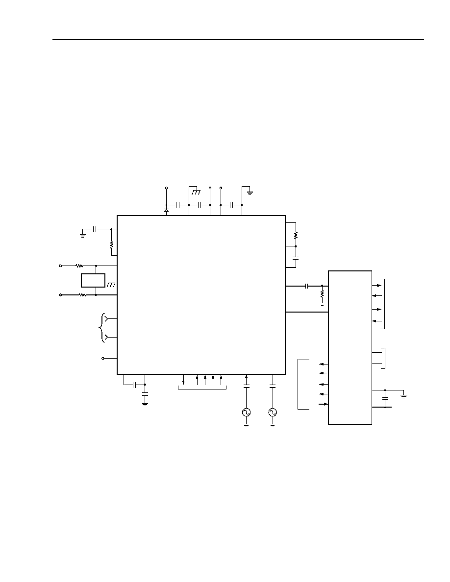
Data Sheet
September 2001
Short-Loop Sine Wave Ringing SLIC
L9215A/G
Agere Systems Inc.
45
ac Applications
(continued)
Design Examples
(continued)
Third-Generation Codec ac Interface Network--Complex Termination
The following reference circuit shows the complete SLIC schematic for interface to the Agere T8536 third-genera-
tion codec. All ac parameters are programmed by the T8536. Note this codec differentiates itself in that no external
components are required in the ac interface to provide a dc termination impedance or for stability. For illustration
purposes, 0.5 Vrms PPM injection was assumed in this example and no meter pulse rejection is used. Also, this
example illustrates the device using programmable overhead and current limit. Please see the T8535/6 data sheet
for information on coefficient programming.
Figure 27. Third-Generation Codec ac Interface Network; Complex Termination
V
BAT1
BGND
V
BAT2
V
CC
AGND
C
BAT1
0.1
�
F
C
BAT2
0.1
�
F
C
CC
0.1
�
F
RTFLT
DCOUT
PR
PT
OVH
V
PROG
V
REF
C
RT
0.1
�
F
R
RT
383
k
AGERE
L7591
V
BAT2
FUSIBLE OR PTC
50
50
CF1
CF2
NSTAT BR B2 B1 B0
C
F1
0.22
�
F
C
F2
0.1
�
F
PPM
0.5 Vrms
C
PPM
10 nF
RING
IN
PPM
IN
VITR
RCVP
RCVN
ITR
VTX
TXI
R
GX
4750
V
BAT1
D
BAT1
V
BAT2
V
CC
C
TX
0.1
�
F
C
RING
0.47
�
F
CONTROL
VOLTAGE
C
C1
PCM
HIGHWAY
DX0
DR0
DX1
DR1
FS
BCLK
DGND
V
DD
SYNC
AND
V
DD
VFXI
VFROP
VFRON
SLIC4a
SLIC3a
SLIC2a
SLIC1a
SLIC0a
CLOCK
L9215G
FROM/TO T8536
CONTROL LATCHES
B2
B1
BR
NSTAT
B0
0.1
�
F
FUSIBLE OR PTC
1/4
R
CIN
20
M
T8536/8

Data Sheet
September 2001
Short-Loop Sine Wave Ringing SLIC
L9215A/G
46
Agere Systems Inc.
ac Applications
(continued)
Design Examples
(continued)
Third-Generation Codec ac Interface Network--Complex Termination (continued)
Table 26. Parts List L9215; Agere T8536 Third-Generation Codec Meter Pulse Application ac and dc
Parameters; Fully Programmable
* For loop stability, increase to 50
minimum if synthesizing 900
or 900
+ 2.16
�
F termination impedance.
Name
Value
Tolerance
Rating
Function
Fault Protection
R
PT
50
1%
Fusible or PTC Protection resistor*.
R
PR
50
1%
Fusible or PTC Protection resistor*.
Protector
Agere L7591
--
--
Secondary protection.
Power Supply
C
BAT1
0.1
�
F
20%
100 V
V
BAT
filter capacitor.
C
BAT2
0.1
�
F
20%
50 V
V
BAT
filter capacitor. |V
BAT2
| < |V
BAT1
|.
D
BAT1
1N4004
--
--
Reverse current.
C
CC
0.1
�
F
20%
10 V
V
CC
filter capacitor.
C
F1
0.22
�
F
20%
100 V
Filter capacitor.
C
F2
0.1
�
F
20%
100 V
Filter capacitor.
Ring/Ring Trip
C
RING
0.47
�
F
20%
10 V
ac-couple input ring signal.
C
RT
0.1
�
F
20%
10 V
Ring trip filter capacitor.
R
RT
383 k
1%
1/16 W
Ring trip filter resistor.
PPM
C
PPM
10 nF
20%
10 V
ac-couple PPM input.
ac Interface
R
GX
4750
1%
1/16 W
Sets T/R to VITR transconductance.
R
CIN
20 M
5%
1/16 W
dc Bias
C
TX
0.1
�
F
20%
10 V
ac/dc separation.
C
C1
0.1
�
F
20%
10 V
dc blocking capacitor.
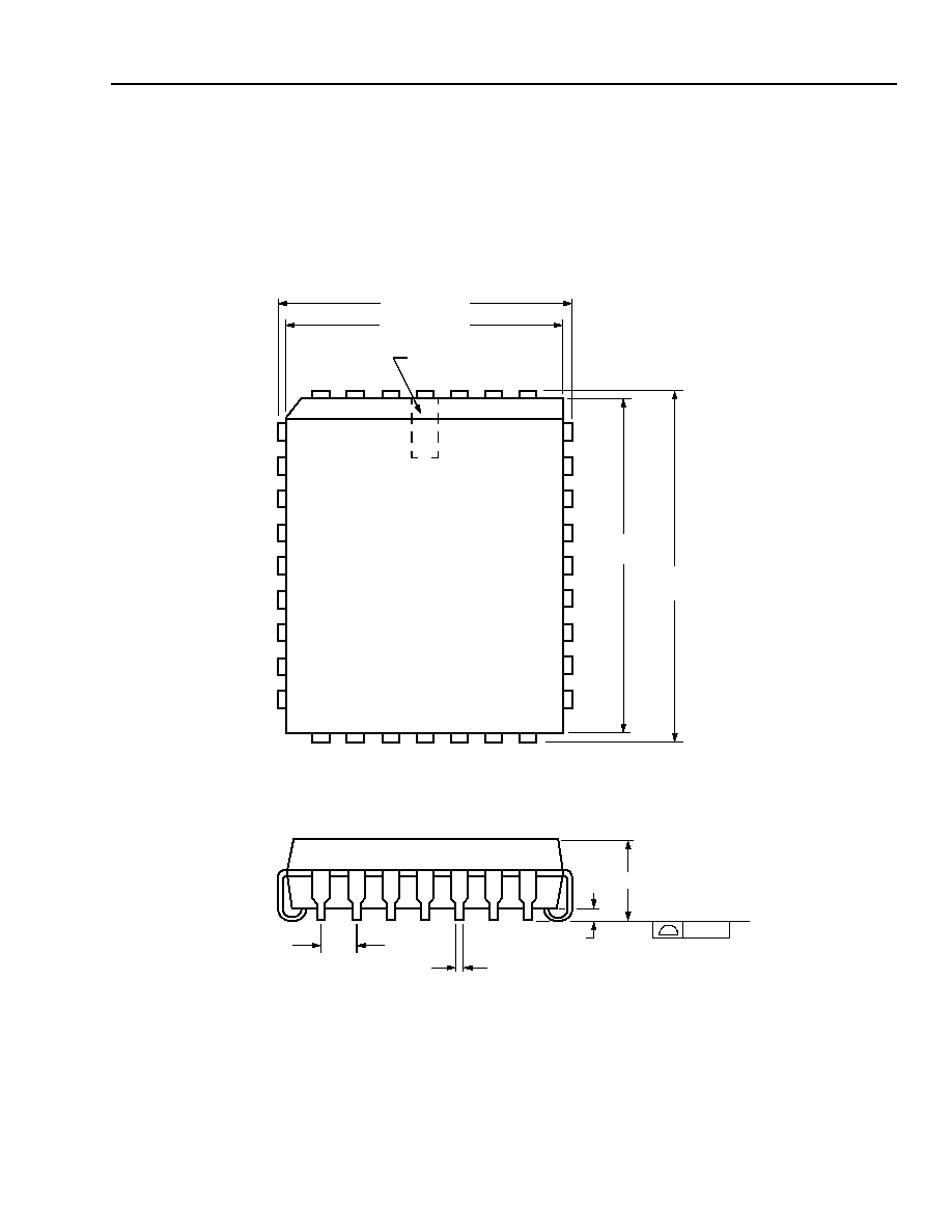
Data Sheet
September 2001
Short-Loop Sine Wave Ringing SLIC
L9215A/G
Agere Systems Inc.
47
Outline Diagrams
32-Pin PLCC
Dimensions are in millimeters.
Note: The dimensions in this outline diagram are intended for informational purposes only. For detailed schemat-
ics to assist your design efforts, please contact your Agere Sales Representative.
5-3813F
0.10
SEATING PLANE
0.38 MIN
TYP
1.27 TYP
0.330/0.533
1
4
30
5
13
21
29
14
20
12.446
�
0.127
11.430
�
0.076
PIN #1 IDENTIFIER
ZONE
14.986
�
0.127
13.970
�
0.076
3.175/3.556
Data Sheet
September 2001
Short-Loop Sine Wave Ringing SLIC
L9215A/G
48
Agere Systems Inc.
Outline Diagrams
(continued)
48-Pin MLCC
Dimensions are in millimeters.
Notes: The dimensions in this outline diagram are intended for informational purposes only. For detailed schemat-
ics to assist your design efforts, please contact your Agere Sales Representative.
The exposed pad on the bottom of the package will be at V
BAT1
potential.
0195mod
PIN #1
IDENTIFIER ZONE
1
7.00
6.75
SEATING PLANE
0.08
0.65/0.80
0.20 REF
DETAIL A
7.00
5.10
� 0.15
3
3.50
3.375
6.75
0.00/0.05
SECTION C�C
11 SPACES @
0.50 = 5.50
0.50 BSC
0.18/0.30
0.30/0.45
0.01/0.05
1.00 MAX
12�
0.18/0.30
0.24/0.60
0.24/0.60
2
1
3
2
0.50 BSC
DETAIL A
C
C
VIEW FOR EVEN TERMINAL/SIDE
C
L
EXPOSED PAD
Data Sheet
September 2001
Short-Loop Sine Wave Ringing SLIC
L9215A/G
Agere Systems Inc.
49
Outline Diagrams
(continued)
48-Pin MLCC, JEDEC MO-220 VKKD-2
Dimensions are in millimeters.
Notes: The dimensions in this outline diagram are intended for informational purposes only. For detailed schemat-
ics to assist your design efforts, please contact your Agere Sales Representative.
The exposed pad on the bottom of the package will be at V
BAT1
potential.
INDEX AREA
7.00
3.50
SEATING PLANE
0.08
0.20 REF
DETAIL A
7.00
5.00/5.25
3.50
11 SPACES @
0.50 = 5.50
0.50 BSC
0.18/0.30
0.02/0.05
1.00 MAX
0.23
0.30/0.50
1
3
2
(7.00/2 x 7.00/2)
PIN #1
IDENTIFIER ZONE
TOP VIEW
SIDE VIEW
DETAIL B
0.23
0.18
0.18
BOTTOM VIEW
2.50/2.625
EXPOSED PAD
DETAIL B
0.50 BSC
DETAIL A
VIEW FOR EVEN TERMINAL/SIDE
C
L

Data Sheet
September 2001
Short-Loop Sine Wave Ringing SLIC
L9215A/G
Agere Systems Inc. reserves the right to make changes to the product(s) or information contained herein without notice. No liab ility is assumed as a result of their use or application.
Copyright � 2001 Agere Systems Inc.
All Rights Reserved
September 2001
DS01-299ALC (Replaces DS01-104ALC)
For additional information, contact your Agere Systems Account Manager or the following:
INTERNET:
http://www.agere.com
E-MAIL:
docmaster@agere.com
N. AMERICA:
Agere Systems Inc., 555 Union Boulevard, Room 30L-15P-BA, Allentown, PA 18109-3286
1-800-372-2447, FAX 610-712-4106 (In CANADA: 1-800-553-2448, FAX 610-712-4106)
ASIA:
Agere Systems Hong Kong Ltd., Suites 3201 & 3210-12, 32/F, Tower 2, The Gateway, Harbour City, Kowloon
Tel. (852) 3129-2000, FAX (852) 3129-2020
CHINA: (86) 21-5047-1212 (Shanghai), (86) 10-6522-5566 (Beijing), (86) 755-695-7224 (Shenzhen)
JAPAN: (81) 3-5421-1600 (Tokyo), KOREA: (82) 2-767-1850 (Seoul), SINGAPORE: (65) 778-8833, TAIWAN: (886) 2-2725-5858 (Taipei)
EUROPE:
Tel. (44) 7000 624624, FAX (44) 1344 488 045
Ordering Information
IEEE
is a registered trademark of The Institute of Electrical and Electronics Engineers, Inc.
PSPICE
is a registered trademark of MicroSim Corporation.
Telcordia Technologies
is a trademark of Bell Communications Research, Inc.
HP
is a trademark of Hewlett-Packard Company.
Device Part No.
Description
Package
Comcode
LUCL9215AAU-D
SLIC Gain = 8
32-Pin PLCC Dry Bag
108327214
LUCL9215AAU-DT
SLIC Gain = 8
32-Pin PLCC Tape & Reel
108327222
LUCL9215GAU-D
SLIC Gain = 2
32-Pin PLCC Dry Bag
108417932
LUCL9215GAU-DT
SLIC Gain = 2
32-Pin PLCC Tape & Reel
108417940
LUCL9215ARG-D
SLIC Gain = 8
48-Pin MLCC Dry Bag
108955451
LUCL9215GRG-D
SLIC Gain = 2
48-Pin MLCC Dry Bag
108955444