
Data Sheet
November 2001
L9217A/G Low-Cost Line Interface
with Reverse Battery and PPM
Features
s
Basic forward/reverse battery SLIC functionality at
a low cost
s
Pin compatible with Agere Systems Inc. L9218/
L9219 SLIC
s
Low active power (typical 154 mW during on-hook
transmission)
s
Low-power scan mode for low-power, on-hook
power dissipation (57 mW typical)
s
Distortion-free, on-hook transmission
s
Convenient operating states:
-- Forward powerup
-- Reverse powerup
-- Low-power scan
-- Disconnect (high impedance)
-- PPM operational states
s
Minimal external components required
s
Two gain options to optimize the codec interface
s
Adjustable supervision functions:
-- Off-hook detector with hysteresis
-- Ring trip detector
s
Adjustable loop current limit
s
Adjustable overhead voltage
s
Ramped rate of battery reversal
s
Periodic pulse metering (PPM) compatible
s
Thermal protection with thermal shutdown indica-
tion
Description
This general-purpose electronic subscriber loop
interface circuit (SLIC) is optimized for low cost, while
still providing a satisfactory set of features. This part
is a pin-for-pin replacement for the Agere L9218/
L9219 SLIC.
The L9217 requires a 5 V power supply and single
battery to operate. This device offers forward and
reverse battery operation. The rate of battery rever-
sal may be ramped to meet international require-
ments. Additionally, a low-power scan mode, wherein
all circuitry except the off-hook supervision is shut
down to conserve power, is available.
The dc current limit may be programmed via a single
external resistor. Both the loop supervision and ring
trip supervision functions are offered with user-
controlled thresholds via external resistors. Over-
head is adequate for 3.14 dBm into 900
of on-hook
transmission.
The device is periodic pulse metering (PPM) compat-
ible, offering a convenient point for meter pulse injec-
tion and filter point for rejection of the meter pulse
signal. In the PPM active modes, overhead voltage is
automatically increased to accommodate on-hook
transmission of meter pulse signals. The level that
the overhead is increased to is set by a single exter-
nal resistor. In this way, the L9217 can accommodate
high-voltage meter pulse signals.
The L9217 is offered with a receive gain that is opti-
mized to interface to a first-generation type codec
(L9217A). It is also offered with a gain option that is
optimized to interface to a third- or fourth-generation
type codec (L9217G). In both cases, minimizing
external components is required at this interface.
Data control is via a parallel data control scheme.
The device is available in a 28-pin PLCC package. It
is built by using a 90 V complementary bipolar
(CBIC) process.

2
Agere Systems Inc.
Data Sheet
November 2001
with Reverse Battery and PPM
L9217A/G Low-Cost Line Interface
Features ......................................................................1
Description...................................................................1
Pin Information ............................................................4
Functional Description .................................................6
Absolute Maximum Ratings (at TA = 25
∞
C) ................7
Recommended Operating Conditions .........................7
Electrical Characteristics .............................................8
Ring Trip Requirements ..........................................12
Test Configurations ...................................................13
Applications ...............................................................15
dc Applications........................................................19
Battery Feed.........................................................19
Overhead Voltage ................................................19
Rate of Battery Reversal ......................................20
Loop Range..........................................................20
Off-Hook Detection...............................................20
Ring Trip Detection...............................................21
Longitudinal Balance...............................................21
Periodic Pulse Metering (PPM)...............................22
ac Design ................................................................23
Codec Types ........................................................23
ac Interface Network ............................................23
Receive Interface .................................................23
Example 1: Real Termination (First-
Generation Codec) ...............................................24
Example 2: Complex Termination (First-
Generation Codec) ...............................................26
Power Derating .......................................................28
Pin-for-Pin Compatibility with L9218/L9219 ............28
PCB Layout Information ............................................28
Outline Diagram.........................................................29
28-Pin PLCC ...........................................................29
Ordering Information..................................................30
Figures
Page
Figure 1.
Functional Diagram...................................3
Figure 2.
28-Pin PLCC.............................................4
Figure 3.
Ring Trip Circuits ....................................12
Figure 4.
L9217 Basic Test Circuit.........................13
Figure 5.
Metallic PSRR.........................................13
Figure 6.
Longitudinal PSRR .................................13
Figure 7.
Longitudinal Balance ..............................14
Figure 8.
RFI Rejection ..........................................14
Figure 9.
Longitudinal Impedance..........................14
Figure 10. ac Gains..................................................14
Figure 11. Basic Loop Start Application
Circuit Using T7504-Type Codec............15
Figure 12. Basic Loop Start Application
Circuit Using T8536-Type Codec............17
Figure 13. Loop Current vs. Loop Voltage .............. 19
Figure 14. Off-Hook Detection Circuit ..................... 20
Figure 15. Ring Trip Equivalent Circuit
and Equivalent Application .................... 21
Figure 16. ac Equivalent Circuit .............................. 24
Figure 17. Interface Circuit Using First-
Generation Codec (±5 V Codec) ........... 27
Figure 18. Interface Circuit Using First-
Generation Codec (5 V Only Codec) ..... 27
Tables
Page
Table 1.
Pin Descriptions ..................................... 4
Table 2.
Input State Coding .................................. 6
Table 3.
Supervision Coding ................................. 6
Table 4.
Power Supply .......................................... 8
Table 5.
2-Wire Port .............................................. 9
Table 6.
Analog Pin Characteristics .................... 10
Table 7.
PPM ...................................................... 10
Table 8.
ac Feed Characteristics ........................ 11
Table 9.
Logic Inputs and Outputs ...................... 12
Table 10.
Parts List for Loop Start Application
Circuit Using T7504-Type Codec .......... 16
Table 11.
900 W Termination, 850 W + 50 nF
Hybrid First-Generation Codec Design
Parameters ........................................... 17
Table 12.
Parts List for Loop Start Application
Circuit Using T8536-Type Codec .......... 18
Table 13.
FB1/FB2 Values vs. Typical Ramp
Time ...................................................... 20
Table of Contents
Contents
Page
Figures
Page
Agere Systems Inc.
3
Data Sheet
November 2001
with Reverse Battery and PPM
L9217A/G Low-Cost Line Interface
Description
(continued)
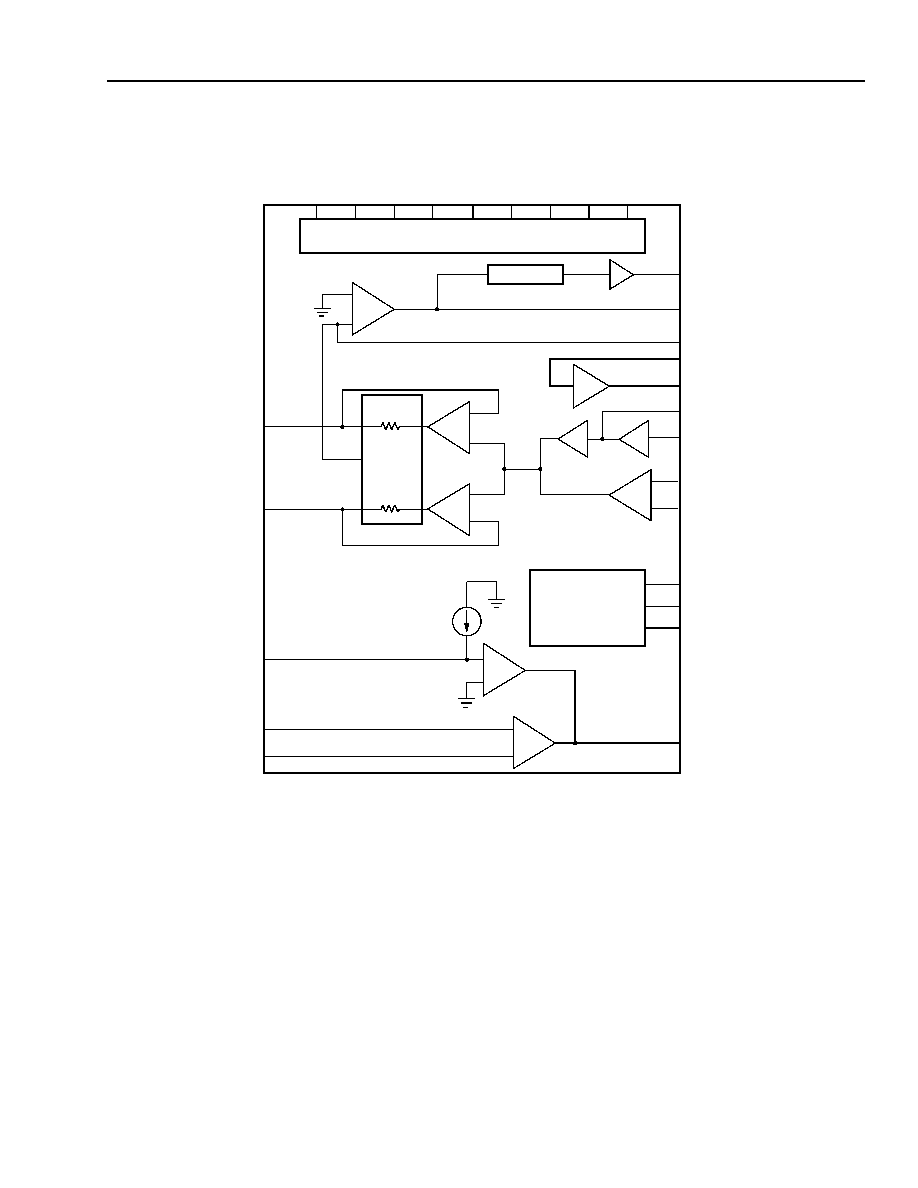
Figure 1. Functional Diagram
≠
+
≠
+
+
≠
A = 1
A = ≠1
POWER CONDITIONING AND REFERENCE
BG
N
D
AG
ND
I
PR
O
G
V
CC
CF
2
PT
PR
RTSN
RTSP
LCTH
RING TRIP DETECTOR
LOOP CLOSURE DETECTOR
BATTERY FEED
STATE CONTROL
B0
RCVP
RCVN
B1
NSTAT
FB2
+
+
≠
≠
TIP/RING
CURRENT
SENSE
B2
A VERSION GAIN = 3.93
G VERSION GAIN = 1
FORWARD AND REVERSE BATTERY
DCOUT
VTX
TG
TXI
VITR
≠
+
AX
RECTIFIER
3
AAC
= 9.66
= 41 V/A
CF
1
FB
1
PPMOUT
PPMIN
OV
H
= 5
PPM
12-3557 (F)
4
Agere Systems Inc.
Data Sheet
November 2001
with Reverse Battery and PPM
L9217A/G Low-Cost Line Interface
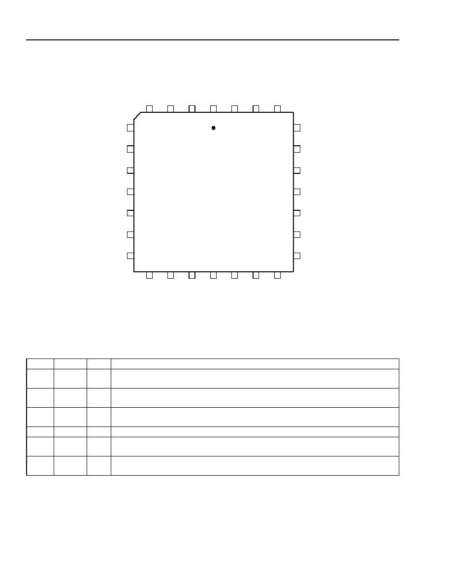
Pin Information
Figure 2. 28-Pin PLCC
Table 1. Pin Descriptions
PLCC Symbol
Type
Description
1
I
PROG
I
Current-Limit Program Input. A resistor to DCOUT sets the dc current limit of the
device.
2
FB2
--
Polarity Reversal Slowdown. Connect a capacitor to ground to control the rate of bat-
tery reversal.
3
FB1
--
Polarity Reversal Slowdown. Connect a capacitor to ground to control the rate of bat-
tery reversal.
4
V
CC
--
5 V Power Supply.
5
RCVP
I
Receive ac Signal Input (Noninverting). This high-impedance input controls the ac
differential voltage on tip and ring.
6
RCVN
I
Receive ac Signal Input (Inverting). This high-impedance input controls the ac differ-
ential voltage on tip and ring.
VTX
TXI
VITR
NSTAT
PPMIN
RTSP
RCVN
DCOUT
V
BAT
PR
5
6
7
8
9
10
11
4
2
1
28
27
3
12
14
15
16
17
18
13
25
24
23
22
21
20
19
I
PR
O
G
B0
CF1
PT
BG
ND
B1
B2
AG
ND
28-PIN PLCC
LCTH
RCVP
CF2
RTSN
OV
H
PPM
O
U
T
FB
2
FB
1
V
CC
26
TG
28-PIN PLCC
12-3558 (F).c

Agere Systems Inc.
5
Data Sheet
November 2001
with Reverse Battery and PPM
L9217A/G Low-Cost Line Interface
Pin Information
(continued)
Table 1. Pin Descriptions (continued)
PLCC
Symbol
Type
Description
7
LCTH
I
Loop Closure Threshold Input. Connect a resistor to DCOUT to set off-hook
threshold.
8
DCOUT
O
dc Output Voltage. This output is a voltage that is directly proportional to the abso-
lute value of the differential tip/ring current.
9
V
BAT
--
Battery Supply. Negative high-voltage power supply.
10
PR
I/O
Protected Ring. The output of the ring driver amplifier and input to loop sensing cir-
cuitry. Connect to the loop through overvoltage protection.
11
CF2
--
Filter Capacitor 2. Connect a 0.1
µ
F capacitor from this pin to AGND.
12
CF1
--
Filter Capacitor 1. Connect a 0.47
µ
F capacitor from this pin to pin CF2.
13
B2
I
State Control Input. B0, B1, and B2 determine the state of the SLIC. See Table 2.
Pin B2 has internal pull-down.
14
B1
I
State Control Input. B0, B1, and B2 determine the state of the SLIC. See Table 2.
Pin B1 has internal pull-down.
15
B0
I
State Control Input. B0, B1, and B2 determine the state of the SLIC. See Table 2.
Pin B0 has internal pull-down.
16
AGND
--
Analog Signal Ground.
17
BGND
--
Battery Ground. Ground return for the battery supply.
18
PT
I/O
Protected Tip. The output of the tip driver amplifier and input to loop sensing cir-
cuitry. Connect to loop through overvoltage protection.
19
RTSN
I
Ring Trip Sense Negative. Connect this pin to the ringing generator signal through a
high-value resistor.
20
RTSP
I
Ring Trip Sense Positive. Connect this pin to the ring relay and the ringer series
resistor through a high-value resistor.
21
PPMIN
I
Receive PPM Signal Input. This high-impedance input controls the PPM differential
voltage on tip and ring. The PPM signal may be present at this pin at all times: how-
ever, PPM will only be transmitted to tip and ring if the appropriate PPM state is cho-
sen. ac couple the PPM signal to this node.
22
NSTAT
O
Ring Trip Detector Output/Loop Detector Output. When low, this logic output indi-
cates that ringing is tripped or that an off-hook condition exists.
23
VITR
O
ac Output Voltage. The voltage at this point is directly proportional to the differential
tip/ring current.
24
TXI
I
ac/dc Separation. Connect a 0.1
µ
F capacitor from this point to VTX.
25
VTX
O
ac Output Voltage. This output is a voltage that is directly proportional to the differ-
ential tip/ring current.
26
TG
--
Transmit Gain. Connect an 8.06 k
from TG to VTX to set the transmit gain of the
SLIC.
27
OVH
I
PPM Overhead. Connect a resistor from this node to ground to set the overhead volt-
age during PPM high overhead modes.
28
PPMOUT
O
PPM Signal Output. Connect a resistor from this node to TG for hybrid cancellation
of the periodic pulse metering (PPM) signal.

6
Agere Systems Inc.
Data Sheet
November 2001
with Reverse Battery and PPM
L9217A/G Low-Cost Line Interface
Functional Description
Table 2. Input State Coding
Table 3. Supervision Coding
B0
B1
B2
State/Definition
1
1
1
Powerup, Forward Battery, Normal Overhead. Normal talk and battery feed state. Pin PT is
positive with respect to PR. On-hook transmission is enabled. PPM is not active. Overhead is un-
affected by resistor OVH and is adequate for 3.14 dBm overload into 900
.
1
0
1
Powerup, Reverse Battery, Normal Overhead. Normal talk and battery feed state. Pin PT is
negative with respect to PR. On-hook transmission is enabled. PPM is not active. Overhead is un-
affected by resistor OVH and is adequate for 3.14 dBm overload into 900
.
1
1
0
Powerup, Forward Battery, High Overhead. Normal talk and battery feed state. Pin PT is posi-
tive with respect to PR. On-hook transmission is enabled. PPM is not active. Overhead is in-
creased via resistor OVH.
1
0
0
Powerup, Reverse Battery, High Overhead. Normal talk and battery feed state. Pin PT is neg-
ative with respect to PR. On-hook transmission is enabled. PPM is not active. Overhead is in-
creased via resistor OVH.
0
1
1
Low-Power Scan. Except for off-hook detection, all circuits are shut down to conserve power. Pin
PT is positive with respect to pin PR. On-hook transmission is disabled.
0
0
1
Disconnect.
The tip and ring amplifiers are turned off, and the SLIC goes to a high-impedance
state (>100 k
). Supervision outputs read on hook. Device will power up in this state.
0
0
0
Powerup, Reverse Battery, High Overhead with PPM. Normal talk and battery feed state. Pin
PT is negative with respect to PR. On-hook transmission is enabled. PPM is active. Overhead is
increased via resistor OVH.
0
1
0
Powerup, Forward Battery, High Overhead with PPM. Normal talk and battery feed state. Pin
PT is positive with respect to PR. On-hook transmission is enabled. PPM is active. Overhead is
increased via resistor OVH.
NSTAT
0 = off-hook or ring trip.
1 = on-hook and no ring trip.

Agere Systems Inc.
7
Data Sheet
November 2001
with Reverse Battery and PPM
L9217A/G Low-Cost Line Interface
Absolute Maximum Ratings
(at T
A
= 25
∞
C)
Stresses in excess of the absolute maximum ratings can cause permanent damage to the device. These are abso-
lute stress ratings only. Functional operation of the device is not implied at these or any other conditions in excess
of those given in the operational sections of the data sheet. Exposure to absolute maximum ratings for extended
periods can adversely affect device reliability.
Note: The IC can be damaged unless all ground connections are applied before, and removed after, all other connections. Furthermore, when
powering the device, the user must guarantee that no external potential creates a voltage on any pin of the device that exceeds the
device ratings. Some of the known examples of conditions that cause such potentials during powerup are the following:
1. An inductor connected to tip and ring can force an overvoltage on V
BAT
through the protection devices if the V
BAT
connection chatters.
2. Inductance in the V
BAT
lead could resonate with the V
BAT
filter capacitor to cause a destructive overvoltage.
Recommended Operating Conditions
Parameter
Symbol
Min
Typ
Max
Unit
5 V Power Supply
V
CC
--
--
7.0
V
Battery (Talking) Supply
V
BAT
--
--
≠75
V
Logic Input Voltage
--
≠0.5
--
7.0
V
Analog Input Voltage
--
≠7.0
--
7.0
V
Maximum Junction Temperature
T
J
150
--
--
∞C
Storage Temperature Range
T
stg
≠40
--
125
∞C
Relative Humidity Range
R
H
5
--
95
%
Ground Potential Difference (BGND to AGND)
--
--
±
3
--
V
PT or PR Fault Voltage (dc)
V
PT
, V
PR
V
BAT
≠ 5
--
3
V
PT or PR Fault Voltage (10 x 1000
µ
s)
V
PT
, V
PR
V
BAT
≠ 15
--
15
V
Current into Ring Trip Inputs
I
RTSP
, I
RTSN
--
±
240
--
µ
A
Parameter
Min
Typ
Max
Unit
Ambient Temperature
≠40
--
85
∞C
V
CC
Supply Voltage
4.75
5.0
5.25
V
V
BAT
Supply Voltage
≠24
≠48
≠70
V

8
Agere Systems Inc.
Data Sheet
November 2001
with Reverse Battery and PPM
L9217A/G Low-Cost Line Interface
Electrical Characteristics
Minimum and maximum values are testing requirements in the temperature range of 25 ∞C to 85 ∞C and battery
range of ≠24 V to ≠70 V. These minimum and maximum values are guaranteed to ≠40 ∞C based on component
simulations and design verification of samples, but devices are not tested to ≠40 ∞C in production. The test circuit
shown in Figure 4 is used, unless otherwise noted. Positive currents flow into the device.
Typical values are characteristics of the device design at 25 ∞C based on engineering evaluations and are not part
of the test requirements. Supply values used for typical characterization are V
CC
= 5.0 V, V
BAT
= ≠48 V, unless oth-
erwise noted.
Table 4. Power Supply
1. This parameter is not tested in production. It is guaranteed by design and device characterization.
2. Airflow, PCB board layers, and other factors can greatly affect this parameter.
Parameter
Min
Typ
Max
Unit
Power Supply--Powerup, No Loop Current:
I
CC
I
BAT
(V
BAT
= ≠48 V)
Power Dissipation (V
BAT
= ≠48 V)
--
--
--
5.2
≠2.66
154
6.5
≠2.95
175
mA
mA
mW
Power Supply--Scan, No Loop Current:
I
CC
I
BAT
(V
BAT
= ≠48 V)
Power Dissipation (V
BAT
= ≠48 V)
--
--
--
3.4
≠0.9
57
4.3
≠1
70
mA
mA
mW
Power Supply--Disconnect, No Loop Current:
I
CC
I
BAT
(V
BAT
= ≠48 V)
Power Dissipation (V
BAT
= ≠48 V)
--
--
--
1.9
≠0.1
14
--
--
--
mA
mA
mW
Power Supply Rejection 500 Hz to 3 kHz
(See Figures 5, 6, 16, and 17.)
1
:
V
CC
V
BAT
30
36
--
--
--
--
dB
dB
Thermal Protection Shutdown (T
jc
)
1
150
165
--
∞
C
Thermal Resistance Still Air, Junction to Ambient (
JA
)
1, 2
:
Natural Convection 2S2P Board
Natural Convection 2S0P Board
Wind Tunnel 100 Linear Feet per Minute (LFPM) 2S2P Board
Wind Tunnel 100 Linear Feet per Minute (LFPM) 2S0P Board
--
--
--
--
30
43
27
36
--
--
--
--
∞
C/W
∞
C/W
∞
C/W
∞
C/W

Agere Systems Inc.
9
Data Sheet
November 2001
with Reverse Battery and PPM
L9217A/G Low-Cost Line Interface
Electrical Characteristics
(continued)
Table 5. 2-Wire Port
1. The longitudinal current is independent of dc loop current.
2. Current-limit I
LIM
is programmed by a resistor, R
PROG
, from pin I
PROG
to DCOUT. I
LIM
is specified at the loop resistance where current limiting
begins (see Figure 13).
3. This parameter is not tested in production. It is guaranteed by design and device characterization.
4. Specification is reduced to |V
BAT1
+ 10.5 V| minimum when V
BAT1
= ≠70 V at 85
∞
C.
5. Longitudinal balance of circuit card will depend on loop series protection resistor matching and magnitude. More information is available in
the Applications section of this document.
Parameter
Min
Typ
Max
Unit
Tip or Ring Drive Current = dc + Longitudinal + Signal
Currents
80
--
--
mA
Signal Current
15
--
--
mArms
Longitudinal Current Capability per Wire
1
8.5
15
--
mArms
dc Loop Current Limit
2
:
Allowed Range Including Tolerance
3
Accuracy (R
LOOP
= 100
, V
BAT
= ≠48 V)
15
--
--
±
5
45
--
mA
%
Powerup Open Loop Voltage Levels (PPMOFF):
Common-mode Voltage
Differential Voltage V
BAT
= ≠48 V
4
(Gain = 2)
Differential Voltage V
BAT
= ≠48 V
4
(Gain = 7.86)
--
|V
BAT
+ 7.5|
|V
BAT
+ 8.0|
V
BAT
/2
|V
BAT
+ 6.5|
|V
BAT
+ 6.5|
--
|V
BAT
+ 5.9|
|V
BAT
+ 5.9|
V
V
V
Powerup Open Loop Voltage Levels (PPMON)
Minimum Programmed Overhead:
Differential Voltage V
BAT
= ≠48 V
(Gain = 7.86)
--
--
|V
BAT
+ 18.67|
V
Disconnect State:
Leakage
--
10
150
µ
A
dc Feed Resistance (for I
LOOP
below regulation level)
(does not include protection resistor)
--
72
100
Loop Resistance Range (≠3.17 dBm overload into
900
; not including protection):
I
LOOP
= 20 mA at V
BAT
= ≠48 V
1800
--
--
Longitudinal to Metallic Balance--
IEEE
Æ
Std. 455
(See Figure 7.)
5
:
200 Hz to 3400 Hz
58
61
--
dB
Metallic to Longitudinal Balance (open loop):
200 Hz to 4 kHz
40
--
--
dB
RFI Rejection (See Figure 8.)
3
, 0.5 Vrms, 50
Source,
30% AM Mod 1 kHz:
500 kHz to 100 MHz
--
--
--
≠55
--
≠45
--
dBV

10
Agere Systems Inc.
Data Sheet
November 2001
with Reverse Battery and PPM
L9217A/G Low-Cost Line Interface
Electrical Characteristics
(continued)
Table 6. Analog Pin Characteristics
1. Loop closure threshold is programmed by resistor R
LCTH
from pin LCTH to pin DCOUT. The programming equation or relationship between
off-hook threshold and resistor value is different for active mode versus scan mode (see Applications section for more details).
2. This parameter is not tested in production. It is guaranteed by design and device characterization.
3. I
N
is the sourcing current at RTSN. Guaranteed if I
N
is within 5
µ
A to 30
µ
A.
Table 7. PPM
* PPM signal should be ac-coupled into PPMIN.
Parameter
Min
Typ
Max
Unit
Differential PT/PR Current Sense (DCOUT):
Gain (PT/PR to DCOUT)
Offset Voltage at I
LOOP
= 0
121
≠100
125
--
129
100
V/A
mV
Loop Closure Detector Threshold (R
LCTH
= 22.1 k
)
1
:
On- to Off-hook Threshold (scan mode)
Off- to On-hook Threshold (active mode)
8.8
6.0
--
--
13.6
10.2
mA
mA
Ring Trip Comparator:
Input Offset Voltage
2
Internal Voltage Source
Current at Input RTSP
3
--
≠9.1
I
N
≠ 0.5
±10
≠8.6
I
N
--
≠8.1
I
N
+ 0.5
mV
V
µ
A
RCVN, RCVP:
Input Bias Current
Input Resistance
--
--
≠0.2
1
≠1
--
µ
A
M
Parameter
Min
Typ
Max
Unit
PPM Source*:
Frequency (f1)
Frequency (f2)
Input Signal
11.88
15.80
0
12
16
--
12.12
16.20
0.525
kHz
kHz
Vrms
Signal Gain (from PPMIN to amplifier outputs)
9
10
11
--
Harmonic Distortion
--
5
--
%
Isolation
50
--
--
dB

Agere Systems Inc.
11
Data Sheet
November 2001
with Reverse Battery and PPM
L9217A/G Low-Cost Line Interface
Electrical Characteristics
(continued)
Table 8. ac Feed Characteristics
1. With a first-generation codec, this parameter is set by external components. Any complex impedance R
1
+ R2 || C between 150
and
1300
can be synthesized. With a third-generation codec, this parameter is set by a codec or by a combination of a codec and an external
network.
2. This parameter is not tested in production. It is guaranteed by design and device characterization.
3. Use this gain option with an Agere first-generation or third-generation codec.
4. Use this gain option with an Agere third-generation codec.
Parameter
Min
Typ
Max
Unit
ac Termination Impedance
1
150
--
1300
Longitudinal Impedance at PT/PR
2
--
0
--
Total Harmonic Distortion--200 Hz to 4 kHz
2
:
Off-hook
On-hook
--
--
--
--
0.3
1.0
%
%
Transmit Gain, f = 1 kHz (PT/PR to VITR) (current limit)
≠391
≠403
≠415
V/A
L9217A, Open Loop:
Receive + Gain, f = 1 kHz (RCVP to PT/PR)
3
Receive ≠ Gain, f = 1 kHz (RCVN to PT/PR)
3
L9217G, Open Loop:
Receive + Gain, f = 1 kHz (RCVP to PT/PR)
4
Receive ≠ Gain, f = 1 kHz (RCVN to PT/PR)
4
7.62
≠7.62
1.94
≠1.94
7.86
≠7.86
2.00
≠2.00
8.09
≠8.09
2.06
≠2.06
--
--
--
--
Gain vs. Frequency (transmit and receive)
(600
termination; reference 1 kHz
2
):
200 Hz to 300 Hz
300 Hz to 3.4 kHz
3.4 kHz to 16 kHz
16 kHz to 266 kHz
≠1.00
≠0.3
≠3.0
--
0.0
0.0
≠0.1
--
0.05
0.05
0.3
2.5
dB
dB
dB
dB
Gain vs. Level (transmit and receive)(reference 0 dBV
2
):
≠55 dB to +3 dB
≠0.05
0
0.05
dB
2-Wire Idle-channel Noise (600
termination):
Psophometric
2
C-message
3 kHz Flat
2
--
--
--
≠87
2
10
≠77
12
20
dBmp
dBrnC
dBrn
Transmit Idle-channel Noise:
Psophometric
2
C-message
3 kHz Flat
2
--
--
--
≠82
7
15
≠77
12
20
dBmp
dBrnC
dBrn
12
12
Agere Systems Inc.
Data Sheet
November 2001
with Reverse Battery and PPM
L9217A/G Low-Cost Line Interface
Electrical Characteristics
(continued)
Table 9. Logic Inputs and Outputs
All outputs are open collectors with internal, 30 k
pull-up resistor. Input pins have internal pull-down or some
method to power up in the disconnect state.
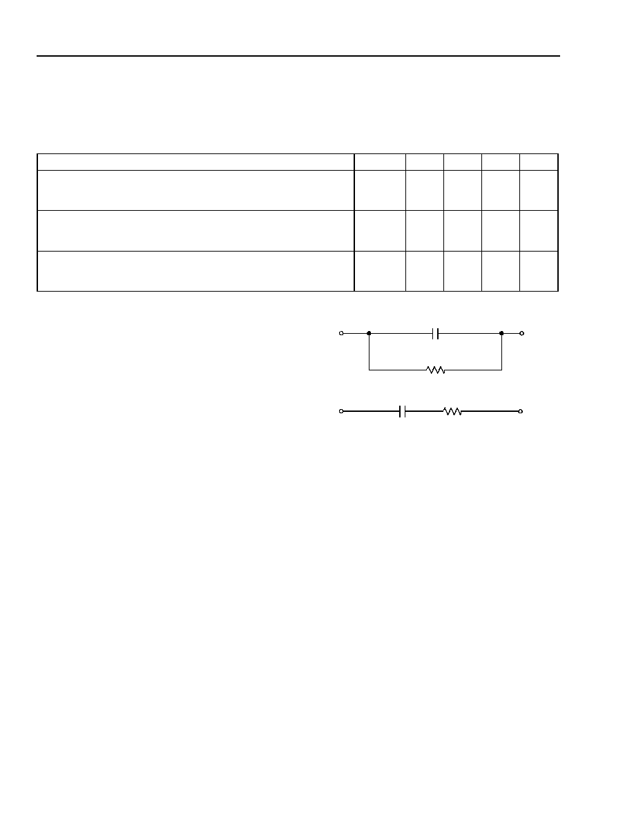
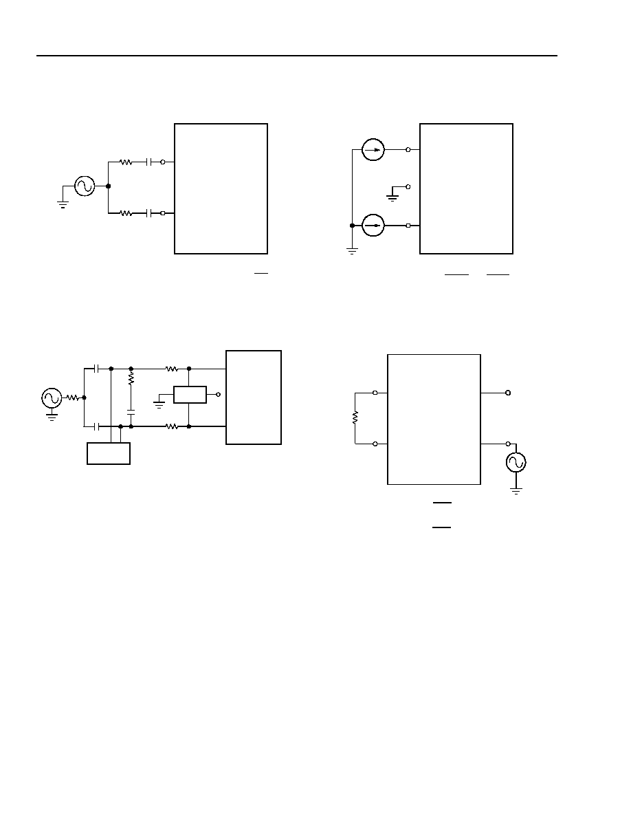
Ring Trip Requirements
s
Ringing signal:
-- Voltage, minimum 35 Vrms, maximum 100 Vrms.
-- Frequency, 17 Hz to 33 Hz.
-- Crest factor, 1.2 to 1.6.
s
Ring trip:
--
100 ms (typical).
s
Pretrip:
-- The circuits in Figure 3 will not cause ring trip.
Figure 3. Ring Trip Circuits
Parameter
Symbol
Min
Typ
Max
Unit
Input Voltages:
Low Level (permissible range)
High Level (permissible range)
V
IL
V
IH
≠0.5
2.0
0.4
2.4
0.7
V
CC
V
V
Input Currents:
Low Level (V
CC
= 5.25 V, V
I
= 0.4 V)
High Level (V
CC
= 5.25 V, V
I
= 2.4 V)
I
IL
I
IH
0
10
4
24
10
50
µ
A
µ
A
Output Voltages (open collector with internal pull-up resistor):
Low Level (V
CC
= 4.75 V, I
OL
= 200
µ
A)
High Level (V
CC
= 4.75 V, I
OH
= ≠20
µ
A)
V
OL
V
OH
0
2.4
0.2
--
0.4
V
CC
V
V
RING
RING
100
10 k
TIP
TIP
2
µ
F
8
µ
F
12-2572 (F).f
Agere Systems Inc.
13
Data Sheet
November 2001
with Reverse Battery and PPM
L9217A/G Low-Cost Line Interface
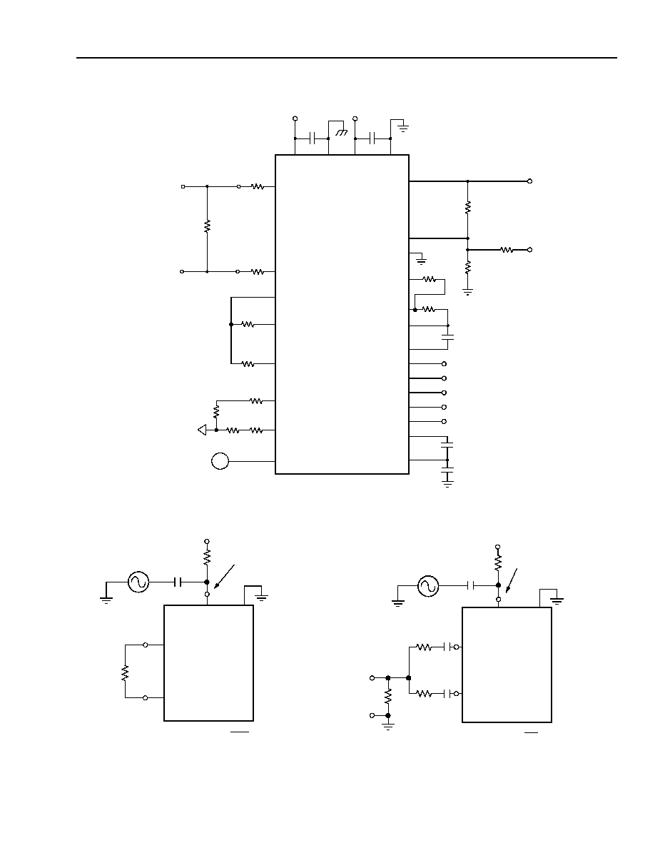
Test Configurations
Figure 4. L9217 Basic Test Circuit
Figure 5. Metallic PSRR
Figure 6. Longitudinal PSRR
V
BAT
V
CC
0.1
µ
F
0.1
µ
F
0.47
µ
F
0.1
µ
F
R
LOOP
43.2 k
22.1 k
B1
NSTAT
V
BAT
BGND V
CC
AGND
I
PROG
LCTH
RTSP
RTSN
VITR
RCVP
B0
CF1
CF2
L9217
SLIC
TG
8.06 k
100
/600
2 M
274 k
2 M
402
V
BAT
50
50
RING
TIP
XMT
75 k
RCV
RCVN
46 k
19.4 k
DCOUT
B2
VTX
TXI
0.1
µ
F
PPMIN
OVH
V
PPMOUT
6.19 k
12-3559 (F).Em
V
S
4.7
µ
F
100
V
BAT
OR
V
CC
DISCONNECT
V
T/R
V
BAT
OR
V
CC
TIP
RING
BASIC
TEST CIRCUIT
+
≠
PSRR = 20log
V
S
V
T/R
900
BYPASS CAPACITOR
12-2582 (F).b
V
S
4.7
µ
F
100
V
BAT
OR
V
CC
DISCONNECT
BYPASS CAPACITOR
56.3
V
BAT
OR V
CC
TIP
RING
BASIC
TEST CIRCUIT
PSRR = 20log
V
S
V
M
67.5
10
µ
F
10
µ
F
67.5
V
M
+
≠
12-2583 (F).b
14
Agere Systems Inc.
Data Sheet
November 2001
with Reverse Battery and PPM
L9217A/G Low-Cost Line Interface
Test Configurations
(continued)
Figure 7. Longitudinal Balance
V
S
= 0.5 Vrms 30% AM 1 kHz modulation,
f = 500 kHz--1 MHz
device in powerup mode, 600
termination.
Figure 8. RFI Rejection
Figure 9. Longitudinal Impedance
Figure 10. ac Gains
TIP
RING
BASIC
TEST CIRCUIT
LONGITUDINAL BALANCE = 20 log
V
S
V
M
368
100
µ
F
100
µ
F
368
V
M
+
≠
V
S
12-2584 (F).c
BASIC TEST
CIRCUIT
TIP
RING
V
BAT
0.01
µ
F
0.01
µ
F
600
2.15
µ
F
82.5
82.5
HP
Æ
4935A
TIMS
50
1
2
4
6, 7
L7591
V
S
5-6756 (F).bm
TIP
RING
BASIC
TEST CIRCUIT
+
≠
+
≠
I
LONG
I
LONG
V
PT
V
PR
Z
LONG
=
OR
V
PT
I
LONG
V
PR
I
LONG
12-2585 (F).a
TIP
RING
BASIC
TEST CIRCUIT
600
V
T/R
+
≠
G
XMT
=
V
XMT
V
T/R
G
RCV
=
V
T/R
V
RCV
XMT
RCV
V
S
12-2587 (F).e
Agere Systems Inc.
15
Data Sheet
November 2001
with Reverse Battery and PPM
L9217A/G Low-Cost Line Interface
Applications
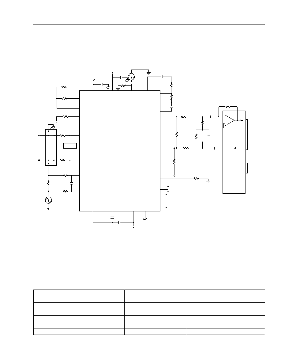
A basic loop start reference circuit, using bused ringing with the L9217 SLIC and the T7504 first-generation codec,
is shown in Figure 11. This circuit is designed for a 900
termination impedance and an 850
+
50 nF transhy-
brid. Transmit gain is set at 0 dBm and receive gain is set at ≠7 dBm.
*
Placeholder for potential resistor to form filter against PPM generator noise if necessary.
Figure 11. Basic Loop Start Application Circuit Using T7504-Type Codec
Table 10 shows the design parameters of the application circuit shown in Figure 11. Components that are adjusted
to program these values are also shown.
Table 10. 900
Termination, 850
+
50 nF Hybrid First-Generation Codec Design Parameters
Design Parameter
Parameter Value
Components Adjusted
Loop Closure Threshold
10 mA
R
LCTH
dc Loop Current Limit
20 mA
R
PROG
ac Termination Impedance
900
R
T1
, R
GP
, R
RCV,
R
GP1
Hybrid Balance Line Impedance
850
+
50 nF
C
HB
, R
HB
, R
HB1
Transmit Gain
0 dBm
R
T2
, R
X,
R
N1,
R
N2,
C
N
Receive Gain
≠7 dBm
R
RCV
, R
GP
, R
T1
2797 (F)
R
PR O G
35.7 k
R
LC TH
22 .1 k
R
PT
50
L7591
R
P R
P T
18
1
7
LC TH
8
D C O U T
50
P R
10
R TS P
20
R
T S1
402
R TS N
19
R
TS N
3.32 M
V
R IN G
V
BA T
C F2
11
C F1
12
C
F 1
0.47
µ
F
A G N D
16
B G N D
17
I
P RO G
V
B AT
9
C
B AT
0.1
µ
F
R C V P
R C V N
5
6
R
G P
R
T1
33.2 k
R
T 2
45.3 k
R
R C V
63.4 k
R
HB 1
97.6 k
R
X
86.6 k
G S X
V F
R
O
D X
D R
FSX
FSR
MCLK
1/4 T7504
CODEC
PCM
HIGHWAY
CONTROL
AND
CLOCK
≠
+
L 9 2 1 7
S L IC
C
R TS 1
0.015
µ
F
R
TS P
2.94 M
C
F2
0.1
µ
F
V
B AT
+ 2.4 V
C
B2
0.47
µ
F
22
SUPERVISION
B 1
B 0
14
15
CONTROL
INPUTS
N S T A T
B 2 13
V IT R
23
T X I
24
V TX
25
TG
26
C
B
0.1
µ
F
R
G P1
8.06 k
TIP
R IN G
E M R
C
B 1
0.47
µ
F
R
HB
86.6 k
C
HB
0.47 n F
14.7 k
C
PP M
0.01
µ
F
P P M IN
R
P PM
6.19 k
R
G N
9.76 k
P P M IN
P P M O U T
28
21
OUTPUT
V
C C
4
C
C C
0.1
µ
F
V
C C
R
O VH
49.9 k
27
O V H (for 2.5 V rm s P P M )
LC A S
C
H Y
4.7 nF
O PEN
R
FLT
*

16
Agere Systems Inc.
Data Sheet
November 2001
with Reverse Battery and PPM
L9217A/G Low-Cost Line Interface
Applications
(continued)
Table 11. Parts List for Loop Start Application Circuit Using T7504-Type Codec
Name
Value
Function
Integrated Circuits
SLIC
L9217
Subscriber loop interface circuit (SLIC).
Protector
Agere L7591
Secondary protection.
Ringing Relay
Agere L7581/2/3 or EMR
Switches ringing signals.
Codec
T7504
First-generation codec.
Overvoltage Protection
R
PT
50
, Fusible
Protection resistor.
R
PR
50
, Fusible
Protection resistor.
Power Supply
C
BAT1
0.1
µ
F, 20%, 100 V
V
BAT
filter capacitor.
C
CC
0.1
µ
F, 20%, 10 V
V
CC
filter capacitor.
C
F1
0.47
µ
F, 20%, 100 V
With C
F2
, improves idle-channel noise.
C
F2
0.1
µ
F, 20%, 100 V
With C
F1
, improves idle-channel noise.
dc Characteristics
R
PROG
35.7 k
, 1%, 1/16 W
Set low current limit.
ac Characteristics
C
B1
0.47
µ
F, 20%, 10 V
ac/dc separation capacitor.
C
B2
0.47
µ
F, 20%, 10 V
ac/dc separation capacitor.
C
B
0.1
µ
F, 20%, 10 V
dc blocking capacitor.
R
T1
33.2 k
, 1%, 1/16 W
With R
GP
and R
RCV
, sets ac termination impedance.
R
RCV
63.4 k
, 1%, 1/16 W
With R
GP
and R
T1
, sets receive gain.
R
GP
14.7 k
, 1%, 1/16 W
With R
T1
and R
RCV
, sets ac termination impedance
and receive gain.
R
T2
45.3 k
, 1%, 1/16 W
With R
X
, sets transmit gain in codec.
R
X
86.6 k
, 1%, 1/16 W
With R
T2
, sets transmit gain in codec.
R
HB1
97.6 k
, 1%, 1/16 W
Sets hybrid balance.
C
HB
0.47 nF, 10%, 10 V
With R
GS
provides gain shaping for hybrid.
R
HB
86.6 k
, 1%, 1/16 W
With C
GS
provides gain shaping for hybrid.
R
GP1
8.06 k
, 1%, 1/16 W
Sets dc transmit gain of SLIC.
R
GN
9.76 k
,
1%, 1/16 W
dc offset.
Meter Pulse
C
HY
4.7 nF, 20%, 10 V
Meter pulse rejection.
C
PPM
0.01
µ
F, 20%, 10 V
Meter pulse injection.
R
PPM
6.19 k
,
1%, 1/16 W
Meter pulse rejection.
R
OVH
49.9 k
,
1%, 1/16 W
Increases PPM overhead mode.
Supervision
R
LCTH
22.1 k
, 1%, 1/16 W
Sets loop closure (off-hook) threshold.
R
TS1
402
, 5%, 2 W
Ringing source series resistor.
C
RTS1
0.015
µ
F, 20%, 10 V
With R
TSN
, R
TSP
, forms filter pole.
R
TSN
3.32 M
, 1%, 1/16 W
With R
TSP
, sets threshold.
R
TSP
2.94 M
, 1%, 1/16 W
With C
RTS1
, R
TSN
, sets threshold.
Agere Systems Inc.
17
Data Sheet
November 2001
with Reverse Battery and PPM
L9217A/G Low-Cost Line Interface
Applications
(continued)
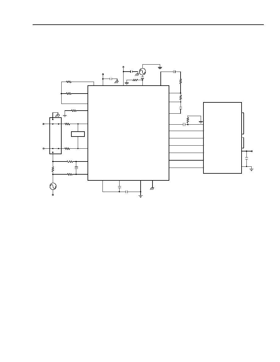
A basic loop start reference circuit, using bused ringing with the L9217 SLIC and the T8536 third-generation codec,
is shown in Figure 12.
*
Placeholder for potential resistor to form filter against PPM generator noise if necessary.
Figure 12. Basic Loop Start Application Circuit Using T8536-Type Codec
R
PROG
35.7 k
R
LCTH
22.1 k
R
PT
50
L7591
R
PR
PT
18
1
7
LCTH
8
DCOUT
50
PR
10
RTSP
20
R
TS1
510
RTSN
19
R
TSN
3.4 M
V
RING
V
BAT
CF2
11
CF1
12
C
F1
0.47
µ
F
AGND
16
BGND
17
L9217
SLIC
C
RTS1
0.015
µ
F
R
TSP
2.94 M
C
F2
0.1
µ
F
RCVN
NSTAT
6
DR2
FS
BCLK
1/4 T8536
PCM
HIGHWAY
CONTROL
AND
CLOCK
B0
B1
15
14
RCVP
5
VF
R
ON
VF
X
I
VF
R
OP
SLIC0a
SLIC3a
SLIC2a
DGND
DX1
DX2
DR1
C
VDD
0.1
µ
F
V
DD
CODEC
B2
13
SLIC4a
22
VITR
23
TIP
RING
EMR
TXI
24
VTX
25
TG
26
C
B
0.1
µ
F
R
GP1
8.06 k
C
B1
0.1
µ
F
TXI
I
PROG
R
PPM
6.19 k
C
PPM
0.01
µ
F
PPMIN
PPMIN
PPMOUT
28
21
V
BAT
9
C
BAT
0.1
µ
F
V
BAT
V
CC
4
C
CC
0.1
µ
F
V
CC
R
OVH
61.9 k
27
OVH (for 3.5 Vrms PPM)
R
CIN
20 M
LCAS
C
HY
4.7 nF
OPEN
R
FLT
*
2798 (F)

18
Agere Systems Inc.
Data Sheet
November 2001
with Reverse Battery and PPM
L9217A/G Low-Cost Line Interface
Applications
(continued)
Table 12. Parts List for Loop Start Application Circuit Using T8536-Type Codec
Name
Value
Function
Integrated Circuits
SLIC
L9217
Subscriber loop interface circuit (SLIC).
Protector
Agere L7591
Secondary protection.
Ringing Relay
Agere L7581/2/3 or EMR
Switches ringing signals.
Codec
T8536
Third-generation codec.
Overvoltage Protection
R
PT
50
, Fusible
Protection resistor.
R
PR
50
, Fusible
Protection resistor.
Power Supply
C
BAT1
0.1
µ
F, 20%, 100 V
V
BAT
filter capacitor.
C
CC
0.1
µ
F, 20%, 10 V
V
CC
filter capacitor.
C
F1
0.47
µ
F, 20%, 100 V
With C
F2
, improves idle-channel noise.
C
F2
0.1
µ
F, 20%, 100 V
With C
F1
, improves idle-channel noise.
dc Characteristics
R
PROG
35.7 k
, 1%, 1/16 W
Set low current limit.
ac Characteristics
C
B1
0.1
µ
F, 20%, 10 V
ac/dc separation capacitor.
C
B
0.1
µ
F, 20%, 10 V
dc blocking capacitor.
R
GP1
8.06 k
, 1%, 1/16 W
Sets dc transmit gain of SLIC.
R
CIN
20 M
, 5%, 1/16 W
dc bias.
Supervision
R
LCTH
22.1 k
, 1%, 1/16 W
Sets loop closure (off-hook) threshold.
R
TS1
510
, 5%, 2 W
Ringing source series resistor.
C
RTS1
0.015
µ
F, 20%, 10 V
With R
TSN
and R
TSP
, forms second 2 Hz filter pole.
R
TSN
3.4 M
, 1%, 1/16 W
With R
TSP
, sets threshold.
R
TSP
2.94 M
, 1%, 1/16 W
With R
TSN
, sets threshold.
Meter Pulse
C
HY
4.7 nF, 20%, 10 V
Meter pulse rejection.
C
PPM
0.01
µ
F, 20%, 10 V
Meter pulse injection.
R
PPM
6.19 k
,
1%, 1/16 W
Meter pulse rejection.
R
OVH
61.9 k
,
1%, 1/16 W
Increases PPM overhead mode.

Agere Systems Inc.
19
Data Sheet
November 2001
with Reverse Battery and PPM
L9217A/G Low-Cost Line Interface
Applications
(continued)
dc Applications
Battery Feed
The dc feed characteristic can be described by:
where:
I
L
= dc loop current.
V
T/R
= dc loop voltage.
|
V
BAT
|
= battery voltage magnitude.
V
OH
= overhead voltage. This is the difference between
the battery voltage and the open loop tip/ring
voltage.
R
L
= loop resistance, not including protection resistors.
R
P
= protection resistor value.
R
dc
= SLIC internal dc feed resistance.
Note: V
BAT
= ≠48 V; I
LIM
= 22 mA; R
dc1
= 115
.
Figure 13. Loop Current vs. Loop Voltage
Starting from the on-hook condition and going through
to a short circuit, the curve passes through the follow-
ing two regions:
Region 1: On-hook and low-loop currents. The slope
corresponds to the dc resistance of the SLIC, R
dc1
(default is 72
typical). The open circuit voltage is
the battery voltage minus the overhead voltage of the
device, V
OH
(default is 6.5 V typical). These values are
suitable for most applications but can be adjusted if
needed.
Region 2: Current limit. The dc current is limited to a
starting value determined by external resistor R
PROG
,
an internal current source, and the gain from tip/ring to
pin VITR. Current limit with a 100
load is set by the
following equation:
0.637 R
PROG
(k
) + 2 mA = I
LIM
x (mA)
Overhead Voltage
In order to drive an on-hook ac signal, the SLIC must
set up the tip and ring voltage to a value less than the
battery voltage. The amount that the open loop voltage
is decreased relative to the battery is referred to as the
overhead voltage. This is expressed as the following
equation:
V
OH
= |V
BAT
| ≠ (V
PT
≠ V
PR
)
Without this buffer voltage, amplifier saturation will
occur and the signal will be clipped. In modes without
PPM, the L9217 is set to allow undistorted on-hook
transmission of a 3.17 dBm signal into a 900
loop
impedance. A minimum 11.1 V overhead is needed to
pass 3.5 Vrms meter pulse.
In high overhead and PPM modes, overhead is auto-
matically increased to accommodate on-hook trans-
mission of meter pulse signals. The increase in
overhead is set by a resistor from pin OVH to ground.
This is expressed as the following equation:
V
OVH
(V) = 6.37 + 0.09535 x R
OVH
(k
)
I
L
V
B AT
V
O H
≠
R
L
2R
P
R
d c
+
+
----------------------------------
=
V
T/R
V
B A T
V
O H
≠
(
)
R
◊
L
R
L
2R
P
R
d c
+
+
---------------------------------------------
=
0
10
20
50
0
20
30
40
50
LOOP VOLTAGE (V)
30
40
10
LOOP CURRE
NT
(m
A)
1
12.5 k
≠1
R
dc1
I
LIM
TESTED
I
LIM
ONSET
12-3050 (F).i
20
20
Agere Systems Inc.
Data Sheet
November 2001
with Reverse Battery and PPM
L9217A/G Low-Cost Line Interface
Applications
(continued)
dc Applications
(continued)
Rate of Battery Reversal
The rate of battery reversal is controlled or ramped by
capacitors FB1 and FB2. A chart showing FB1/FB2 val-
ues versus typical ramp rate is given below. Leave
FB1/FB2 open if it is not desired to ramp the rate of
battery reversal.
Table 13. FB1/FB2 Values vs. Typical Ramp Time
Loop Range
The equation below can be rearranged to provide the
loop range for a required loop current:
Off-Hook Detection
The loop closure detection threshold is set by resistor
R
LCTH
. The supervision output bit NSTAT is high in an
on-hook condition. The off-hook comparator goes low
during an off-hook condition:
Figure 14. Off-Hook Detection Circuit
C
FB1
/C
FB2
Transition Time
0.01
µ
F
20 ms
0.1
µ
F
220 ms
0.22
µ
F
440 ms
0.47
µ
F
900 ms
1.0
µ
F
1.8 s
1.22
µ
F
2.25 s
1.3
µ
F
2.5 s
1.4
µ
F
2.7 s
1.6
µ
F
3.2 s
R
L
V
B A T
V
O H
≠
I
L
----------------------------
2R
P
≠
R
D C
≠
=
I
TR
(mA) = 0.4167 R
LTCH
(k
) ≠1.9 mA
ACTIVE off-hook to on-hook
I
TR
(mA) = 0.4167 R
LTCH
(k
) + 2.7 mA
SCAN on-hook to off-hook
R
L
ITR
R
P
R
P
RING
≠
+
≠
+
DCOUT
R
LCTH
LCTH
NSTAT
TIP
0.125 V/mA
0.05 mA
12-2553 (F)
Agere Systems Inc.
21
Data Sheet
November 2001
with Reverse Battery and PPM
L9217A/G Low-Cost Line Interface
Applications
(continued)
dc Applications
(continued)
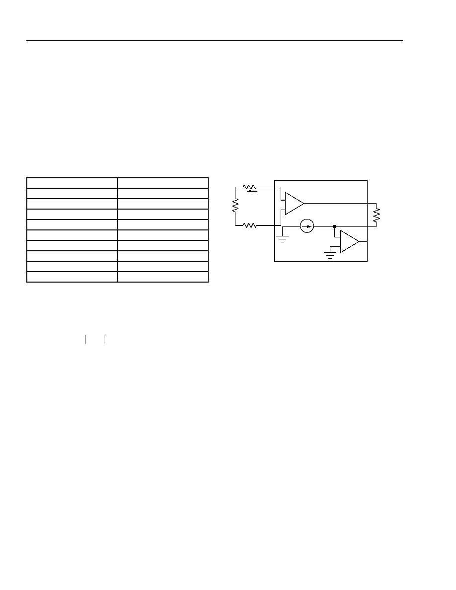
Ring Trip Detection
The ring trip circuit is a comparator that has a special input section optimized for this application. The equivalent
circuit is shown in Figure 15, along with its use in an application using unbalanced, battery-backed ringing.
Figure 15. Ring Trip Equivalent Circuit and Equivalent Application
Ring trip detection threshold is given by the following equation:
I
TH
(mA) =
Longitudinal Balance
The SLIC is graded to certain longitudinal balance specifications. The numbers are guaranteed by testing (Figure 5
and Figure 8). However, for specific applications, the longitudinal balance may also be determined by termination
impedance, protection resistance, and especially by the mismatch between protection resistors at tip and ring. This
can be illustrated by the following equation:
LB = 20 x log
where:
LB: longitudinal balance.
RP: protection resistor value in
.
ZT: magnitude of the termination impedance in
.
: protection resistor mismatch in
.
: SLIC internal tip/ring sensing mismatch.
The
can be calculated using the above equation with these exceptions:
=
0, ZT = 600
,
RP = 100
,
and the
longitudinal balance specification on a specific code.
Now with
available, the equation will predict the actual longitudinal balance for RP, ZT, and
.
Be aware that ZT may vary with frequency for complex impedance applications.
+
≠
R
TSP
R
LOOP
15 k
8.6 V
I
P
= I
N
R
TSN
3.32 M
/
3.40 M
C
RTS1
0.015
µ
F
PHONE
HOOK SWITCH
RC PHONE
V
RING
V
BAT
NSTAT
R
TSP
I
N
R
TSN
≠
+
2.94 M
R
S
402
/
510
2799 (F)
RTSN M
(
)
0.015 RTSP M
(
)
≠
+
[
]
V
BAT
8.6
≠
[
]
◊
1000
◊
RTSN M
(
)
0.015
+
[
]
R
S
◊
-------------------------------------------------------------------------------------------------------------------------------------------------------------------------
368
RP
+
(
)
368
ZT RP
≠
+
(
)
◊
368
2
ZT 2
≠
RP
◊
[
]
◊
+
◊
(
)
◊
-------------------------------------------------------------------------------------------

22
Agere Systems Inc.
Data Sheet
November 2001
with Reverse Battery and PPM
L9217A/G Low-Cost Line Interface
Applications
(continued)
Periodic Pulse Metering (PPM)
Periodic pulse metering (PPM), also referred to as
TTX, is input to the PPMIN input of the L9217. Upon
application of appropriate logic control, this signal is
presented to the tip/ring subscriber loop. The state of
the L9217 may be changed while applying PPM sig-
nals. The L9217 assumes that a shaped PPM signal is
applied to the PPMIN input.
Sufficient drive current is available in the tip and ring
drive amplifiers to support 3.5 Vrms PPM signals into a
200
load with a 45 mA dc current limit.
PPM signals are input to a separate PPMIN input. This
input is controlled via the logic table. PPMIN is off dur-
ing all states except the forward/reverse PPM active
state. Thus, PPM signals may be present at all times,
even during non-PPM active times. To apply PPM to
tip/ring, from a normal overhead state first switch to a
high overhead state without PPM; the overhead volt-
age at tip/ring will increase to 7 V to 13 V. The ramp up
time of the overhead increase is on the order of hun-
dreds of milliseconds. Thus, wait 1 s before applying
the PPM signal by going to a PPM active high over-
head state. Once in a high overhead, there is no timing
requirement in switching in and out of a PPM active
mode. Without the initial 1 s delay, AT/AR will get into
saturation and PPM signal at T/R will get distorted, pro-
ducing crosstalk in the handset.
PPM input signals may be a maximum 0.525 Vrms at
PPMIN. The gain from PPMIN tip/ring is 10. Thus, for
2.5 Vrms at tip and ring, apply a 0.375 Vrms signal at
PPMIN. The PPM signal should be ac coupled to
PPMIN through a 0.01
µ
F capacitor.
When applied to tip and ring, the PPM signal will also
be returned through the SLIC and will appear at the
SLIC VITR output. The concern is that this high-voltage
signal can overload the codec input and cause distor-
tion of the (desired) ac signal. Therefore, some sort of
PPM rejection scheme must be employed, see Figure
1. The L9217 outputs on the PPMOUT pin, which is the
output of the PPM input amplifier. Connecting a resis-
tor, R
PPM,
from PPMOUT to node TG will provide a path
for a hybrid reject of the returned meter pulse signal.
The return path from tip and ring to VITR for the PPM
signal is through the internal AX amplifier. TG is the
input to this amplifier. Through R
PPM
, by applying a
PPM signal equal in magnitude, but 180 degrees out of
phase to the returned PPM signal at TG, the PPM sig-
nal is cancelled, preventing overload at the codec
input. Even if the cancellation is not perfect, the idea is
to reduce the PPM signal so as not to overload the
codec. Codecs typically have a low-pass filter at their
input to reject any residual meter pulse signal.
The value of R
PPM
is selected by:
R
PPM
=
[{(V
PPMIN
x
10)/(R
PPMLOAD
+
R
DC
+
2R
P
)}/201.2]
≠1
For undistorted transmission of meter pulse signals,
increase the overhead as described in the Overhead
Voltage section of this data sheet.

Agere Systems Inc.
23
Data Sheet
November 2001
with Reverse Battery and PPM
L9217A/G Low-Cost Line Interface
Applications
(continued)
ac Design
Codec Types
At this point in the design, the codec needs to be
selected. The interface network between the SLIC and
codec can then be designed. There are four key ac
design parameters. Termination impedance is the
impedance looking into the 2-wire port of the line card.
It is set to match the impedance of the telephone loop
in order to minimize echo return to the telephone set.
Transmit gain is measured from the 2-wire port to the
PCM highway, while receive gain is done from the PCM
highway to the transmit port. Finally, the hybrid balance
network cancels the unwanted amount of the receive
signal that appears at the transmit port.
Below is a brief codec feature summary.
First-Generation Codecs. These perform the basic fil-
tering, A/D (transmit), D/A (receive), and
µ
-law/A-law
companding. They all have an op amp in front of the
A/D converter for transmit gain setting and hybrid bal-
ance (cancellation at the summing node). Depending
on the type, some have differential analog input stages,
differential analog output stages, 5 V only or
±
5 V oper-
ation, and
µ
-law/A-law selectability. These are avail-
able in single and quad designs. This type of codec
requires continuous time analog filtering via external
resistor/capacitor networks to set the ac design param-
eters. An example of this type of codec is the Agere
T7504 quad 5 V only codec.
This type of codec tends to be the most economical in
terms of piece part price, but tends to require more
external components than a third-generation codec.
Furthermore, ac parameters are fixed by the external
R/C network, so software control of ac parameters is
difficult.
Third-Generation Codecs. This class of devices
includes all ac parameters set digitally under micropro-
cessor control. Depending on the device, it may or may
not have data control latches. Additional functionality
sometimes offered includes tone plant generation and
reception, TTX generation, test algorithms, and echo
cancellation. Again, this type of codec may be 5 V
only or
±
5 V operation, single quad or 16-channel, and
µ
-law/A-law or 16-bit linear coding selectable. Exam-
ples of this type of codec are the Agere T8535/6 (5 V
only, quad, standard features), T8533/4 (5 V only, quad
with echo cancellation), and the T8531/36 (5 V only
16-channel with self-test).
ac Interface Network
The ac interface network between the L9217 and the
codec will vary depending on the codec selected. With
a first-generation codec, the interface between the
L9217 and codec actually sets the ac parameters. With
a third-generation codec, all ac parameters are set dig-
itally, internal to the codec; thus, the interface between
the L9217 and this type of codec is designed to avoid
overload at the codec input in the transmit direction,
and to optimize signal-to-noise ratio (S/N) in the
receive direction.
Receive Interface
Because the design requirements are very different
with a first- or third-generation codec, the L9217 is
offered with two different receive gains. Each receive
gain was chosen to optimize, in terms of external com-
ponents required, the ac interface between the L9217
and the codec.
With a first-generation codec, the termination imped-
ance is set by providing gain shaping through a feed-
back network from the SLIC VITR output to the SLIC
RCVN/RCVP inputs. The L9217 provides a transcon-
ductance from T/R to VITR in the transmit direction and
a single ended to differential gain in the receive direc-
tion from either RCVN or RCVP to T/R. Assuming a
short from VITR to RCVN or RCVP, the maximum
impedance that is seen looking into the SLIC is the
product of the SLIC transconductance times the SLIC
receive gain, plus the protection resistors. The various
specified termination impedance can range over the
voice band as low as 300
up to over 1000
. Thus, if
the SLIC gains are too low, it will be impossible to syn-
thesize the higher termination impedances. Further-
more, the termination that is achieved will be far less
than what is calculated by assuming a short for SLIC
output to SLIC input. In the receive direction, in order to
control echo, the gain is typically a loss, which requires
a loss network at the SLIC RCVN/RCVP inputs, which
will reduce the amount of gain that is available for ter-
mination impedance. For this reason a high-gain SLIC
is required with a first-generation codec.

24
24
Agere Systems Inc.
Data Sheet
November 2001
with Reverse Battery and PPM
L9217A/G Low-Cost Line Interface
Applications
(continued)
ac Design
(continued)
Receive Interface (continued)
With a third-generation codec, the line card designer
has different concerns. To design the ac interface, the
designer must first decide upon all termination imped-
ance, hybrid balances, and transmission level points
(TLP) requirements that the line card must meet. In the
transmit direction, the only concern is that the SLIC
does not provide a signal that is too hot and overloads
the codec input. Thus, for the highest TLP that is being
designed to, given the SLIC gain, the designer, as a
function of voice band frequency, must ensure that the
codec is not overloaded. With a given TLP and a given
SLIC gain (if the signal will cause a codec overload),
the designer must insert some sort of loss, typically a
resistor divider, between the SLIC output and codec
input.
In the receive direction, the issue is to optimize S/N.
Again, the designer must consider all the considered
TLPs. The idea is, for all desired TLPs, to run the
codec at or as close as possible to its maximum output
signal, to optimize the S/N. Remember noise floor is
constant, so the hotter the signal from the codec, the
better the
S/N. The problem is, if the codec is feeding a high-gain
SLIC, either an external resistor divider is needed to
knock the gain down to meet the TLP requirements, or
the codec is not operating near maximum signal levels,
thus compromising the S/N.
It appears the solution is to have a SLIC with a low
gain, especially in the receive direction. This will allow
the codec to operate near its maximum output signal
(to optimize S/N), without an external resistor divider
(to minimize cost).
Note also that some third-generation codecs require
the designer to provide an inherent resistive termina-
tion via external networks. The codec will then provide
gain shaping, as a function of frequency to meet the
return loss requirements. Further stability issues may
add external components or excessive ground plane
requirements to the design.
To meet the unique requirements of both types of
codecs, the L9217 offers two receive gain choices.
These receive gains are mask programmable at the
factory and are offered as two different code variations.
For interface with a first-generation codec, the L9217A
is offered with a receive gain of 7.86. For interface with
a third-generation codec, the L9217G is offered with a
receive gain of 2. In either case, the transconductance
in the transmit direction, or the transmit gain is 403
.
Example 1: Real Termination (First-Generation Codec)
ac equivalent circuits for real termination using a T7504 codec is shown in Figure 15.
Figure 16. ac Equivalent Circuit
R
P
Z
T
+
≠
R
P
V
T/R
I
T/R
V
S
Z
T/R
+
≠
RING
A
V
= ≠1
A
V
= 1
VITR
≠
+
+
≠
CURRENT
SENSE
TIP
+
≠
R
T1
R
RCV
R
HB1
R
T2
RCVN
RCVP
R
X
VGSX
VF
X
IN
VFR
1/4 T7504 CODEC
R
G
2.4 V
≠0.403 V/mA
A
V
=
L9217 SLIC
VF
X
IP
3.93
12-3581 (F).Cm

Agere Systems Inc.
25
Data Sheet
November 2001
with Reverse Battery and PPM
L9217A/G Low-Cost Line Interface
Applications
(continued)
ac Design
(continued)
Example 1: Real Termination (First-Generation Codec) (continued)
The following design equations refer to the circuit in Figure 16. Use these to synthesize real termination imped-
ance.
Termination Impedance:
Z
T
=
Receive Gain:
g
rcv
=
g
rcv
=
Transmit Gain:
g
tx
=
g
tx
=
x
Hybrid Balance:
h
bal
= 20log
To optimize the hybrid balance, the sum of the currents at the VFX input of the codec op amp should be set to 0.
The following expressions assume the test network is the same as the termination impedance:
R
HB
=
h
bal
= 20log
V
T R
/
I
T R
/
≠
--------------
Z
T
2R
P
3168
1
R
T 3
R
G P
---------
R
T 3
R
R C V
------------
+
+
-----------------------------------
+
=
V
T R
/
V
fr
--------------
7.86
1
R
RCV
R
T3
---------------
R
RCV
R
GP
---------------
+
+
1
Z
T
Z
T/R
-------------
+
-------------------------------------------------------------------------------------
V
GSX
V
T R
/
---------------
R
X
R
T6
----------
403
Z
T
-----------
V
GSX
V
T R
/
---------------
R
X
g
tx
g
rcv
◊
-------------------------
R
X
R
HB
------------
g
tx
≠
g
rcv
◊

26
Agere Systems Inc.
Data Sheet
November 2001
with Reverse Battery and PPM
L9217A/G Low-Cost Line Interface
Applications
(continued)
ac Design
(continued)
Example 2: Complex Termination (First-Generation Codec)
Below are design equations for complex termination (see Figure 17 and Figure 18).
R
TGP
|| R
TGS
R
TGP
|| R
TGS
g
tx
=
g
rcv =
h
bal
= 20log
where:
Z
T/R
= R
1
+ R
2
|| C
Z
TG
= R
TGP
|| (R
TGS
+ C
G
)
R
TGP
= 8.06 k
R
TGS
=
R
TGP
C
G
=
x C
and
C
N
R
N2
=
C
G
R
TGP
R
N1
= R
N2
The equations above do not include the blocking capacitors.
R
T 1
2R
P
7.86
201.2
------------
1
1
R
T 3
R
G P
---------
R
T 3
R
R C V
------------
+
+
-----------------------------------
1
1
R
N 1
R
N 2
--------
+
------------------
≠
∑
+
=
R
T 2
7.86
201.2
------------
R
T G P
R
T G S
/
1
R
T 3
R
G P
---------
R
T 3
R
R C V
------------
+
+
-----------------------------------
1
1
R
N 1
R
N 2
--------
+
------------------
+
+
=
1
C
T
-------
7.86
201.2
----------------
1
C
N1
-----------
R
N2
R
N1
R
N2
+
(
)
2
-------------------------------------
R
TGP
R
TGS
||
1
C
TG
-----------
R
TGP
R
TGP
R
TGS
+
-------------------------------------
2
∑
∑
1
1
R
T3
R
GP
------------
R
T3
R
RCV
---------------
+
+
----------------------------------------------
1
1
R
N1
R
N2
-----------
+
---------------------
≠
+
=
R
X
R
T6
----------
1
201.2
----------------
Z
TG
Z
T
-----------
7.86
1
R
RCV
R
T3
---------------
R
RCV
R
GP
---------------
+
+
------------------------------------------------
1
1
Z
T
Z
T R
/
-------------
+
------------------------
◊
R
X
R
HB
------------
g
tx
≠
g
rcv
◊
R
1
R
2
-------
R
2
2
R
TGP
R
1
R
2
+
(
)
------------------------------------------
2R
P
3167
-------------
3167
2R
P
-------------
R
T GS
R
T GP
--------------
1
≠
Agere Systems Inc.
27
Data Sheet
November 2001
with Reverse Battery and PPM
L9217A/G Low-Cost Line Interface
Applications
(continued)
ac Design
(continued)
Example 2: Complex Termination (First-Generation Codec) (continued)
Figure 17. Interface Circuit Using First-Generation Codec (±5 V Codec)
Figure 18. Interface Circuit Using First-Generation Codec (5 V Only Codec)
R
TGS
R
TGP
= 8.06 k
R
T6
R
X
R
T3
CODEC
OP AMP
≠
+
C
N
R
N1
R
N2
R
GP
R
RCV
R
CVN
R
CVP
≠I
T/R
201.2
C
GS
C
B1
R
TGS
R
T6
R
T3
CODEC
OUTPUT
DRIVE
AMP
CODEC
OP AMP
≠
+
C
N
R
N1
R
RCV
RCVN
RCVP
≠I
T/R
C
GS
AX
5-6401 (F).l
R
TGS
C
B1
R
TGP
= 8.06 k
R
T6
R
x
R
T3
CODEC
OUTPUT
DRIVE
AMP
CODEC
OP AMP
≠
+
C
N
R
N1
R
N2
R
GP
R
RCV
RCVN
RCVP
≠I
T/R
201.2
C
G
AX
≠2.4 V
C
B2
5-6400 (F).o

28
Agere Systems Inc.
Data Sheet
November 2001
with Reverse Battery and PPM
L9217A/G Low-Cost Line Interface
Applications
(continued)
Power Derating
Operating temperature range, maximum current limit,
maximum battery voltage, minimum dc loop, and pro-
tection resistor values will influence the overall thermal
performance. This section shows the relevant design
equations and considerations in evaluating the SLIC
thermal performance.
Consider the L9217 SLIC in a 28-pin PLCC package.
The thermal resistance on a 2-layer board with natural
convection is 43 ∞C/W.
The SLIC will enter the thermal shutdown state at a
minimum of 150
∞C. The thermal shutdown design
should ensure that the SLIC temperature does not
reach 150
∞
C under normal operating conditions.
Assume a maximum ambient operating temperature of
85 ∞C, a design current limit of 25 mA, and a maximum
battery of ≠52 V. Furthermore, assume a (worst-case)
minimum dc loop of 200
, and that 50
protection
resistors are used at both tip and ring.
1. T
TSD
≠ T
AMBIENT(max)
= allowed thermal rise.
150 ∞C ≠ 85 ∞C = 65 ∞C
2. Allowed thermal rise = package thermal
impedance
∑
SLIC power dissipation.
65 ∞C = 43 ∞C/W
∑
SLIC power dissipation
SLIC power dissipation (P
DISS
) = 1.51 W
Thus, if the total power dissipated in the SLIC is less
than 1.51 W, it will not enter the thermal shutdown
state. Total SLIC power is calculated as:
Total P
DISS
= Maximum battery
∑
maximum
current limit (including effects of accuracy)
+ SLIC quiescent power
For the L9217, SLIC quiescent power (P
Q
) is maximum
at 0.175 W. Thus,
Total P
DISS
= (≠52 V
∑
[25 mA
∑
1.08])
+ 0.175 W
Total P
DISS
= 1.404 W + 0.175 W
Total P
DISS
= 1.579 W
The power dissipated in the SLIC is the total power dis-
sipation minus the power that is dissipated in the loop.
SLIC P
DISS
= Total power ≠ loop power
Loop power = (I
LIM
)
2
∑
(R
dcLOOP
min + 2R
P
)
Loop power = (25 mA
∑
1.08)
2
∑
(200
+ 100
)
Loop power = 0.219 W
SLIC power = 1.579 W ≠ 0.219 W = 1.36
SLIC power = 1.36 W < 1.51 W
Thus, in this example, the thermal design ensures that
the SLIC will not enter the thermal shutdown state.
Pin-for-Pin Compatibility with L9218/L9219
The L9217 can be a pin-for-pin replacement for the
L9218/L9219. The exceptions are as follows: L9217
has three logic control inputs: B0, B1, and B2. The
L9218 has only two logic control inputs: B0 and B1. Pin
13 in L9218 is NC, so a connection between the con-
troller and pin 13 will not affect L9218 operation. In
L9217, pin 28 is PPMOUT, pin 21 is PPMIN, and pin 27
is OVH. In L9218/9, pin 28 is NC, pin 21 is NC, and pin
27 is TSD
PCB
Layout Information
Make the leads to BGND and V
BAT
as wide as possible
for thermal and electrical reasons. Also, maximize the
amount of PCB copper in the area of (and specifically
on) the leads connected to this device for the lowest
operating temperature.
When powering the device, make certain that no exter-
nal potential creates a voltage on any pin of the device
that exceeds the device ratings. In this application,
some of the conditions that cause such potentials dur-
ing powerup are the following:
1. An inductor connected to PT and PR (this can force
an overvoltage on V
BAT
through the protection
devices if the V
BAT
connection chatters).
2. Inductance in the V
BAT
lead (this could resonate
with the V
BAT
filter capacitor to cause a destructive
overvoltage).
This device is normally used on a circuit card that is
subjected to hot plug-in, meaning the card is plugged
into a biased backplane connector. In order to prevent
damage to the IC, all ground connections must be
applied before, and removed after, all other connec-
tions.
Agere Systems Inc.
29
Data Sheet
November 2001
with Reverse Battery and PPM
L9217A/G Low-Cost Line Interface
Outline Diagram
28-Pin PLCC
Dimensions are in millimeters.
1.27 TYP
0.330/0.533
0.10
SEATING PLANE
0.51 MIN
TYP
4.572
MAX
12
18
11
5
4
1
26
25
19
12.446
±
0.127
PIN #1 IDENTIFIER
ZONE
11.506
±
0.076
11.506
±
0.076
12.446
±
0.127
5-2506 (F) r.8

Data Sheet
November 2001
with Reverse Battery and PPM
L9217A/G Low-Cost Line Interface
Agere Systems Inc. reserves the right to make changes to the product(s) or information contained herein without notice. No liability is assumed as a result of their use or application.
Copyright © 2001 Agere Systems Inc.
All Rights Reserved
November 2001
DS02-038ALC (Replaces DS02-002ALC)
For additional information, contact your Agere Systems Account Manager or the following:
INTERNET:
http://www.agere.com
E-MAIL:
docmaster@agere.com
N. AMERICA:
Agere Systems Inc., 555 Union Boulevard, Room 30L-15P-BA, Allentown, PA 18109-3286
1-800-372-2447, FAX 610-712-4106 (In CANADA: 1-800-553-2448, FAX 610-712-4106)
ASIA:
Agere Systems Hong Kong Ltd., Suites 3201 & 3210-12, 32/F, Tower 2, The Gateway, Harbour City, Kowloon
Tel. (852) 3129-2000, FAX (852) 3129-2020
CHINA: (86) 21-5047-1212 (Shanghai), (86) 10-6522-5566 (Beijing), (86) 755-695-7224 (Shenzhen)
JAPAN: (81) 3-5421-1600 (Tokyo), KOREA: (82) 2-767-1850 (Seoul), SINGAPORE: (65) 778-8833, TAIWAN: (886) 2-2725-5858 (Taipei)
EUROPE:
Tel. (44) 7000 624624, FAX (44) 1344 488 045
Ordering Information
IEEE
is a registered trademark of The Institute of Electrical and Electronics Engineers, Inc.
HP
is a registered trademark of Hewlett-Packard Company.
Device
Package
Comcode
LUCL9217AAR-DT
28-Pin PLCC
(Tape & Reel, Dry-bagged)
Gain of 8
108760737
LUCL9217AAR-D
28-Pin PLCC
(Dry-bagged)
Gain of 8
108760729
LUCL9217GAR-DT
28-Pin PLCC
(Tape & Reel, Dry-bagged)
Gain of 2
108760760
LUCL9217GAR-D
28-Pin PLCC
(Dry-bagged)
Gain of 2
108760752