 | ÐлекÑÑоннÑй компоненÑ: LUCL9500 | СкаÑаÑÑ:  PDF PDF  ZIP ZIP |
Äîêóìåíòàöèÿ è îïèñàíèÿ www.docs.chipfind.ru

Preliminary
Data Sheet
September 2001
L9500A
High-Voltage Ringing SLIC for VoIP Applications
L9500A Introduction
The Agere Systems Inc. L9500A is a subscriber line
interface circuit that is optimized for short-loop,
power-sensitive applications. This device provides
the complete set of line interface functionality (includ-
ing power ringing) needed to interface to a subscriber
loop. This device has the capability to operate with a
V
CC
supply of 3.3 V or 5 V and is designed to mini-
mize external components required at all device
interfaces. This device is optimized to interface to
data over cable service interface specification (DOC-
SIS) compliant cable modem gateway, multi-media
adaptor, and residential gateway products, such as
the
Broadcom
®
BCM3351, BCM3352, BCM6352,
and BCM1101 and equivalent products.
Features
s
Differential ringing and codec interface
s
Onboard ringing generation
s
Three ringing input options:
-- Sine wave
-- PWM
-- Logic level square wave
s
Flexible V
CC
options:
-- 5 V or 3.3 V V
CC
-- No 5 V required
s
Battery switch to minimize off-hook power
s
Eight operating states:
-- Scan mode for minimal power dissipation
-- Forward and reverse battery active
-- On-hook transmission states
-- Ground start
-- Ring mode
-- Disconnect mode
s
Ultralow on-hook power:
-- 27 mW scan mode
-- 38 mW active mode
s
Loop start, ring trip, and ground start detection
s
Software-controllable dual current limit option
s
28-pin PLCC package
s
48-pin MLCC package
Applications
s
Interface to
Broadcom
:
-- BCM3351 Cable Modem
-- BCM3352 Cable Modem
-- BCM6352 Integrated Multi-Media Adaptor
-- BCM1101 Residential Gateway
s
Cable Modem
s
Voice over Internet Protocol (VoIP)
s
Voice over DSL
s
Remote Subscriber Units
s
Broadband Wireless
s
Short Loop Access
Description
This device is optimized to provide battery feed, ring-
ing, and supervision on short-loop plain old tele-
phone service (POTS) loops.
This device provides power ring to the subscriber
loop through amplification of a low-voltage input. It
provides forward and reverse battery feed states, on-
hook transmission, a low-power scan state, ground
start (tip open), and a forward disconnect state.
The device requires a V
CC
and battery to operate.
V
CC
may be either a 5 V or a 3.3 V supply. The ring-
ing signal is derived from the high-voltage battery. A
battery switch is included to allow for use of a lower-
voltage battery in the off-hook mode, thus minimizing
short-loop off-hook power.
Ring mode overhead is collapsed, allowing rail-to-rail
operation. In this manner, the L9500 can operate
from a lower 75 V battery to minimize critical power
consumption and at the same time extend subscriber
ringing loop lengths to 500
and beyond.
Loop closure, ring trip, and ground start detection is
available. The loop closure detector has a fixed
threshold with hysteresis. The ring trip detector
requires a single-pole filter, thus minimizing external
components required.
The dc current limit is set and fixed by a logic-control-
lable pin. Ground or open applied to this pin sets the
current limit at the low or high value.
The device is offered with differential ringing and
receive input, making it ideal for direct interface to
DOCSIS compliant cable modem gateway products.

Preliminary Data Sheet
September 2001
High-Voltage Ringing SLIC for VoIP Applications
L9500A
2
Agere Systems Inc.
Table of Contents
Contents
Page
L9500A Introduction ..................................................................................................................................................1
Features ..................................................................................................................................................................1
Applications.............................................................................................................................................................1
Description ..............................................................................................................................................................1
Features ....................................................................................................................................................................4
Description.................................................................................................................................................................4
Architecture Diagram .................................................................................................................................................6
Pin Information ..........................................................................................................................................................7
Operating States........................................................................................................................................................9
State Definitions ......................................................................................................................................................10
Forward Active ......................................................................................................................................................10
Reverse Active ......................................................................................................................................................10
Scan ......................................................................................................................................................................10
On-Hook Transmission--Forward Battery ............................................................................................................10
On-Hook Transmission--Reverse Battery ............................................................................................................10
Disconnect ............................................................................................................................................................10
Ring.......................................................................................................................................................................10
Ground Start .........................................................................................................................................................10
Thermal Shutdown ................................................................................................................................................10
Absolute Maximum Ratings (@ T
A
= 25 °C) ............................................................................................................11
Electrical Characteristics .........................................................................................................................................12
Test Configurations .................................................................................................................................................19
Applications .............................................................................................................................................................21
Power Control .......................................................................................................................................................21
dc Loop Current Limit............................................................................................................................................22
Overhead Voltage .................................................................................................................................................22
Active Mode .......................................................................................................................................................22
Scan Mode .........................................................................................................................................................22
On-Hook Transmission Mode.............................................................................................................................22
Ring Mode ..........................................................................................................................................................22
Loop Range ..........................................................................................................................................................22
Battery Reversal Rate ...........................................................................................................................................23
Supervision ...........................................................................................................................................................23
Loop Closure.........................................................................................................................................................23
Ring Trip ...............................................................................................................................................................23
Ground Start .........................................................................................................................................................23
Power Ring ...........................................................................................................................................................24
Sine Wave Input Signal and Sine Wave Power Ring Signal Output ..................................................................24
ac Applications ........................................................................................................................................................25
ac Parameters.......................................................................................................................................................25
Design Examples ..................................................................................................................................................26
First-Generation Codec ac Interface Network--Resistive Termination..............................................................26
Broadcom
3352 Interface Network........................................................................................................ .............26
Outline Diagrams.....................................................................................................................................................28
28-Pin PLCC .........................................................................................................................................................28
48-Pin MLCC ........................................................................................................................................................29
48-Pin MLCC, JEDEC MO-220 VKKD-2...............................................................................................................30
Ordering Information ...............................................................................................................................................31

Preliminary Data Sheet
September 2001
High-Voltage Ringing SLIC for VoIP Applications
L9500A
Agere Systems Inc.
3
Table of Contents
Figures
Page
Figure 1. Architecture Diagram ................................................................................................................................6
Figure 2. 28-pin PLCC Diagram ...............................................................................................................................7
Figure 3. 48-pin MLF Diagram .................................................................................................................................7
Figure 4. Basic Test Circuit .................................................................................................................................... 19
Figure 5. Metallic PSRR ......................................................................................................................................... 20
Figure 6. Longitudinal PSRR .................................................................................................................................. 20
Figure 7. Longitudinal Balance ............................................................................................................................... 20
Figure 8. ac Gains .................................................................................................................................................. 20
Figure 9. Ringing Waveform Crest Factor = 1.6 ..................................................................................................... 24
Figure 10. Ringing Waveform Crest Factor = 1.2 ................................................................................................... 24
Figure 11. RING
IN
Operation .................................................................................................................................. 25
Figure 12. Reference Schematic with
Broadcom
BCM Embedded Codec Devices and Agere
L9500 SLIC ........................................................................................................................................... 26
Tables
Page
Table 1. Pin Descriptions ........................................................................................................................................8
Table 2. Control States .............................................................................................................................................9
Table 3. Supervision Coding .....................................................................................................................................9
Table 4. Recommended Operating Characteristics .............................................................................................. 11
Table 5. Thermal Characteristics ............................................................................................................................11
Table 6. Environmental ........................................................................................................................................... 12
Table 7. 5 V Supply Currents .................................................................................................................................. 12
Table 8. 5 V Powering .............................................................................................................................................12
Table 9. 3.3 V Supply Currents .............................................................................................................................. 13
Table 10. 3.3 V Powering ....................................................................................................................................... 13
Table 11. 2-Wire Port .............................................................................................................................................14
Table 12. Analog Pin Characteristics .................................................................................................................... 15
Table 13. ac Feed Characteristics ........................................................................................................................ 16
Table 14. Logic Inputs and Outputs (V
CC
= 5 V) ................................................................................................... 17
Table 15. Logic Inputs and Outputs (V
CC
= 3.3 V) ................................................................................................ 17
Table 16. Ground Start ........................................................................................................................................... 17
Table 17. Ringing Specifications ............................................................................................................................18
Table 18. Ring Trip ................................................................................................................................................. 18
Table 19. Typical Active Mode On- to Off-Hook Tip/Ring Current-Limit Transient Response ............................... 22
Table 20. FB1 and FB2 Values vs. Typical Ramp Time ........................................................................................ 23
Table 21. Parts List L9500; Agere L9500 and
Broadcom
BCM3352 (per
Broadcom
BCM93552SV Application
Board--SLIC Daughter Boad Components); Fully Programmable ........................................................ 27

Preliminary Data Sheet
September 2001
High-Voltage Ringing SLIC for VoIP Applications
L9500A
4
Agere Systems Inc.
Features
s
On board balanced ringing generation:
-- No ring relay
-- No bulk ring generator required
-- 15 Hz to 70 Hz ring frequency supported
-- Sine wave input-sine wave output
-- PWM input-sine wave output
-- Square wave input-trapezoidal output
s
Power supplies requirements:
-- V
CC
talk battery and ringing battery required
-- No 5 V supply required
-- No high-voltage positive supply required
s
Flexible Vcc options:
-- 5 V or 3.3 V V
CC
operation
-- 5 V or 3.3 V V
CC
interchangeable and transparent
to users
s
Battery switch via logic control:
-- Minimize off-hook power dissipation
s
Minimal external components required
s
Eight operating states:
-- Forward active, V
BAT2
applied
-- Polarity reversal active, V
BAT2
applied
-- On-hook transmission, V
BAT1
applied
-- On-hook transmission polarity reversal, V
BAT1
applied
-- Ground start
-- Scan
-- Forward disconnect
-- Ring mode
s
Unlatched parallel data control interface
s
Ultralow SLIC power:
-- Scan 38 mW (V
CC
= 5 V)
-- Forward/reverse active 54 mW (V
CC
= 5 V)
-- Scan 27 mW (V
CC
= 3.3 V)
-- Forward/reverse active 41 mW (V
CC
= 3.3 V)
s
Supervision:
-- Loop start, fixed threshold with hysteresis
-- Ring trip, single-pole ring trip filtering, fixed thresh-
old as a function of battery voltage
-- Ground start fixed threshold with hysteresis
s
Adjustable current limit:
-- 25 mA or 40 mA via ground or open to control
input
s
Overhead voltage:
-- Clamped typically <51 V differentially
-- Clamped maximum <56.5 V single-ended
s
Thermal shutdown protection with hysteresis
s
Device interfaces:
-- Differential receive interface
-- Singled-ended transmit interface
-- Differential ring input
s
Package options:
-- 28-pin PLCC
-- 48-pin MLCC
s
90 V CBIC-S technology
Description
The L9500 is designed to provide battery feed, ringing,
and supervision functions on short plain old telephone
service (POTS) loops. This device is designed for
ultralow power in all operating states.
The L9500 offers 8 operating states. The device
assumes use of a lower-voltage talk battery, a higher-
voltage ringing battery, and a V
CC
supply.
The L9500 requires only a positive V
CC
supply. No
5 V supply is needed. The L9500 can operate with a
V
CC
of either 5 V or 3.3 V, allowing for greater user flex-
ibility. The choice of V
CC
voltage is transparent to the
user; the device will function with either supply voltage
connected.
Two batteries are used:
1. A high-voltage ring battery (V
BAT1
).
V
BAT1
is a maximum 75 V. V
BAT1
is used for power
ring signal amplification and for scan, on-hook
transmission, and ground start modes. This supply
is current limited to approximately the maximum
power ringing current, typically 50 mA.
2. A lower-voltage talk battery (V
BAT2
).
V
BAT2
is used for active mode powering.

Preliminary Data Sheet
September 2001
High-Voltage Ringing SLIC for VoIP Applications
L9500A
Agere Systems Inc.
5
Description
(continued)
Forward and reverse battery active modes are used for
off-hook conditions. Since this device is designed for
short-loop applications, the lower-voltage V
BAT2
is
applied during the forward and reverse active states
.
Battery reversal is quiet, without breaking the ac path.
Rate of battery reversal may be ramped to control
switching time.
The magnitude of the overhead voltage in the forward
and reverse active modes has a typical default value of
7.0 V, allowing for an on-hook transmission of an undis-
torted signal of 3.14 dBm into 900
. Additionally, this
allows sufficient overhead for 500 mV of meter pulse if
desired. This overhead is fixed. The ring trip detector is
turned off during active modes to conserve power.
Because on-hook transmission is not allowed in the
scan mode, an on-hook transmission mode is defined.
This mode is functionally similar to the active mode,
except the tip ring voltage is derived from the higher
V
BAT1
rather than V
BAT2
.
In the on-hook transmission modes with a primary bat-
tery whose magnitude is greater than a nominal
51 V, the magnitude of the tip-to-ground and ring-to-
ground voltage is clamped at less than 56.5 V.
To minimize on-hook power, a low-power scan mode is
available. In this mode, all functions except off-hook
supervision are turned off to conserve power. On-hook
transmission is not allowed in the scan mode.
In the scan mode with a primary battery whose magni-
tude is greater than a nominal 51 V, the magnitude of
the tip-to-ground and ring-to-ground voltage is clamped
at less than 56.5 V.
A forward disconnect mode is provided, where all cir-
cuits are turned off and power is denied to the loop.
The device offers a ring mode, in which a power ring
signal is provided to the tip/ring pair. During the ring
mode, a user-supplied, low-voltage ring signal is differ-
entially input to the device's RING
IN
input. This signal is
amplified to produce the power ring signal. This signal
may be a sine wave or filtered square wave to produce
a sine wave on trapezoidal output. Ring trip detector
and common-mode current detector are active during
the ring mode.
With maximum V
BAT1
and a sine wave input, the L9500
has sufficient power to ring a 5 REN (1386
+ 40
µ
F)
ringing load into 500
of physical resistance.
This feature eliminates the need for a separate external
ring relay, associated external circuitry, and a bulk ring-
ing generator. See the Applications section of this data
sheet for more information.
Both the ring trip and loop closure supervision func-
tions are included. The loop closure has a fixed typical
10.5 mA on- to off-hook threshold in the active mode
and a fixed 11.5 mA on- to off-hook threshold from the
scan mode. In either case, there is a 2 mA hysteresis.
The ring trip detector requires only a single-pole filter at
the input, minimizing external components. The ring
trip threshold at a given battery voltage is fixed. Typical
ring trip threshold is 42.5 mA for a 70 V V
BAT1.
The device offers a ground start mode. In this mode the
tip drive amplifier is turned off. The device presents a
high impedance (>100 k
) to PT and a current limited
battery (V
BAT1
) to PR. V
BAT1
is clamped to less than
56.5 V in this mode at PR. The NSTAT loop current
detctor is used for ring ground detection. In the ground
start mode, since the loop current is common mode,
the loop closure threshold is reduced in half, thus main-
taining loop supervision at specified levels.
Upon reaching the thermal shutdown temperature, the
device will enter an all off mode. Upon cooling, the
device will re-enter the state it was in prior to thermal
shutdown. Hysteresis is built in to prevent oscillation.
Data control is via a parallel unlatched control scheme.
The dc current limit is fixed to either 25 mA or 40 mA
depending if ground or open is applied to the V
PROG
current limit programming pin. Programming accuracy
is ±8%.
Circuitry is added to the L9500 to minimize the inrush
of current from the V
CC
supply and to the battery supply
during an on- to off-hook transition, thus saving in
power supply design cost. See the Applications section
of this data sheet for more information.
The L9500 uses a voltage feed-current sense architec-
ture; thus the transmit gain is a transconductance. The
L9500 transconductance is set via a single external
resistor, and this device is designed for optimal perfor-
mance with a transconductance set at 300 V/A. This
interface is single ended. The L9500 offers a differen-
tial receive interface with a gain of 8.
The L9500 is internally referenced to 1.5 V. This refer-
ence voltage is output at the V
REF
output of the device.
The SLIC output VITR is also referenced to 1.5 V. The
SLIC inputs RCVP/RCVN
are floating inputs.
The L9500 is packaged in a 28-pin PLCC or a 48-pin
MLCC package.
Preliminary Data Sheet
September 2001
High-Voltage Ringing SLIC for VoIP Applications
L9500A
6
Agere Systems Inc.
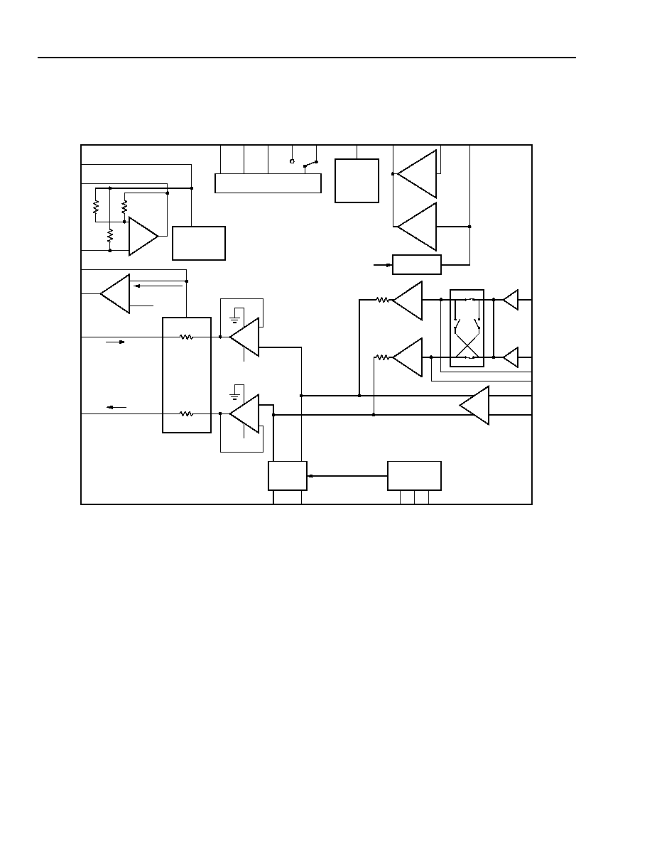
Architecture Diagram
12-3530.F (F)
Figure 1. Architecture Diagram
V
REF
VITR
TXI
ITR
VTX
PR
PT
CF2
CF1
FB2
FB1
POWER
AGND
V
CC
BGND
V
BAT2
V
BAT1
V
PROG
NSTAT
RTFLT
DCOUT
1.5 V
BAND-GAP
REFERENCE
AAC
B = 20
OUT
(ITR/306)
TIP/RING
CURRENT
SENSE
+1
RFT
18
RFR
18
V
REG
1
V
REG
RINGING
35x
PARALLEL
DATA
INTERFACE
RING
INN
B0
B1
B2
X1
X1
RCVN
RCVP
CURRENT
LIMIT
AND
INRUSH
CONTROL
RING
LOOP
RECTIFIER
VITR
TRIP
CLOSURE
V
REF
+
+
+
+
GAIN
AX
ac INTERFACE
RING
INP
GAIN = 4

Preliminary Data Sheet
September 2001
High-Voltage Ringing SLIC for VoIP Applications
L9500A
Agere Systems Inc.
7
Pin Information
12-3558e
Figure 2. 28-pin PLCC Diagram
12-3361.b
Figure 3. 48-pin MLF Diagram
B0
B1
B2
PR
PT
FB1
RING
INP
CF2
CF1
RTFLT
5
6
7
8
9
10
11
4
2
1
28
27
3
12
14
15
16
17
18
13
25
24
23
22
21
20
19
NST
A
T
V
BAT
2
AG
ND
V
PR
O
G
NC
V
BAT
1
V
CC
BG
ND
L9500
DCOUT
RING
INN
V
REF
FB2
VTX
TXI
VIT
R
RCVP
RCVN
26
IT
R
28-PIN PLCC
PINOUT
1
3
4
6
7
8
9
10
11
12
2
48
46
45
44
43
42
41
40
38
37
47
13
16
17
18
19
20
21
22
23
24
14
36
33
32
31
30
29
28
27
26
25
35
B2
PT
FB1
RING
INP
AGN
D
RING
INN
PR
RC
V
N
NS
T
A
T
RC
V
P
TX
I
IT
R
FB2
BGN
D
V
RE
F
V
BA
T
2
VIT
R
34
VT
X
39
15
5
DCOUT
CF2
CF1
RTFLT
V
CC
V
BA
T
1
V
PR
O
G
B1
B0
35
L9500
48-PIN MLCC
PINOUT
NC
NC
NC
NC
NC
NC
NC
NC
NC
NC
NC
NC
NC
NC
NC
NC
NC
NC
NC
NC
NC

Preliminary Data Sheet
September 2001
High-Voltage Ringing SLIC for VoIP Applications
L9500A
8
Agere Systems Inc.
Pin Information
(continued)
Table 1. Pin Descriptions
28-Pin
PLCC
48-Pin
MLCC
Symbol Type
Name/Function
1
43
NSTAT
O
Loop Closure Detector Output--Ring Trip Detector Output.
When low, this logic output indicates that an off-hook condition
exists or ringing is tripped or a ring ground has occurred.
2
45
VITR
O
Transmit ac Output Voltage. Output of internal AAC amplifier.
This output is a voltage that is directly proportional to the differ-
ential ac tip/ring current.
3
47
RCVP
I
Receive ac Signal Input (Noninverting). This high-impedance
input controls to ac differential voltage on tip and ring. This node
is a floating input.
4
48
RCVN
I
Receive ac Signal Input (Inverting). This high-impedance
input controls to ac differential voltage on tip and ring. This node
is a floating input.
5
1
RING
INN
I
Power Ring Signal Input. Couple to a sine wave or lower crest
factor low-voltage ring signal. The input here is amplified to pro-
vide the full power ring signal at tip and ring. This signal may be
applied continuously, even during nonringing states.
6
2
RING
INP
I
Power Ring Signal Input. Couple to a sine wave or lower crest
factor low-voltage ring signal. The input here is amplified to pro-
vide the full power ring signal at tip and ring. This signal may be
applied continuously, even during nonringing states.
7
6
DCOUT
O
dc Output Voltage. This output is a voltage that is directly pro-
portional to the absolute value of the differential tip/ring current.
This is used to set ring trip threshold.
8
8
CF2
--
Filter Capacitor. Connect a capacitor from this node to ground.
9
10
CF1
--
Filter Capacitor. Connect a capacitor from this node to CF2.
10
12
RTFLT
--
Ring Trip Filter. Connect this lead to DCOUT via a resistor and
to AGND with a capacitor to filter the ring trip circuit to prevent
spurious responses. A single-pole filter is needed.
11
13
V
REF
O
SLIC Internal Reference Voltage. Output of internal 1.5 V ref-
erence voltage.
12
15
AGND
GND
Analog Signal Ground.
13
16
V
CC
PWR
Analog Power Supply. User choice of 5 V or 3.3 V nominal
power or supply.
14
19
V
BAT1
PWR
Battery Supply 1. High-voltage battery.
15
21
V
BAT2
PWR
Battery Supply 2. Lower-voltage battery.
16
23
BGND
GND
Battery Ground. Ground return for the battery supplies.
17
3, 4, 5, 7, 9, 11,
14, 17, 18, 20,
22, 27, 29, 30,
32, 36, 37, 40,
42, 44, 46
NC
--
No Connection.
18
24
V
PROG
I
Current-Limit Program Input. Connect ground to this pin to set
current limit to 25 mA; leave this pin open to set current limit to
40 mA.

Preliminary Data Sheet
September 2001
High-Voltage Ringing SLIC for VoIP Applications
L9500A
Agere Systems Inc.
9
Pin Information
(continued)
Table 1. Pin Descriptions (continued)
Operating States
Table 2. Control States
Table 3. Supervision Coding
28-Pin
PLCC
48-Pin
MLCC
Symbol Type
Name/Function
19
25
FB2
--
Polarity Reversal Slowdown Capacitor. Connect a capacitor
from this node for controlling rate of battery reversal. If ramped bat-
tery reversal is not desired, this pin is left open.
20
26
FB1
--
Polarity Reversal Slowdown Capacitor. Connect a capacitor
from this node for controlling rate of battery reversal. If ramped bat-
tery reversal is not desired, this pin is left open.
21
28
PT
I/O
Protected Tip. The output drive of the tip amplifier and input to the
loop sensing circuit. Connect to loop through overvoltage and
overcurrent protection.
22
31
PR
I/O
Protected Ring. The output drive of the ring amplifier and input to
the loop sensing circuit. Connect to loop through overvoltage and
overcurrent protection.
23
33
B2
I
u
State Control Input. These pins have an internal 100 k
pull-up.
24
34
B1
I
u
State Control Input. These pins have an internal 100 k
pull-up.
25
35
B0
I
u
State Control Input. These pins have an internal 100 k
pull-up.
26
38
ITR
I
Transmit Gain. Input to AX amplifier. Connect a 4.75 k
resistor
from this node to VTX to set transmit gain. Gain shaping for termi-
nation impedance with a first generation codec is also achieved
with a network from this node to VTX.
27
39
VTX
O
ac Output Voltage. Output of internal AX amplifier. The voltage at
this pin is directly proportional to the differential tip/ring current.
28
41
TXI
I
ac/dc Separation. Input to internal AAC amplifier. Connect a
0.1
µ
F capacitor from this pin to VTX.
B0
B1
B2
State
0
0
1
Forward active
0
1
1
Reverse active
0
0
0
On-hook transmission forward battery
0
1
0
On-hook transmission reverse battery
1
1
0
Ground start
1
0
0
Scan
1
1
1
Disconnect--device will power up in this state
1
0
1
Ring
NSTAT
0 = off-hook or ring trip or thermal shutdown or ring ground.
1 = on-hook and no ring trip and no thermal shutdown and no ring ground.

Preliminary Data Sheet
September 2001
High-Voltage Ringing SLIC for VoIP Applications
L9500A
10
Agere Systems Inc.
State Definitions
Forward Active
s
Pin PT is positive with respect to PR.
s
V
BAT2
is applied to tip/ring drive amplifiers.
s
Loop closure and common-mode detect are active.
s
Ring trip detector is turned off to conserve power.
s
Overhead is set to nominal 6.0 V for undistorted
transmission of 3.14 dBm into 900
.
Reverse Active
s
Pin PR is positive with respect to PT.
s
V
BAT2
is applied to tip/ring drive amplifiers.
s
Loop closure and common-mode detect are active.
s
Ring trip detector is turned off to conserve power.
s
Overhead is set to nominal 6.0 V for undistorted
transmission of 3.14 dBm into 900
.
Scan
s
Except for loop closure, all circuits (including ring trip
and common-mode detector) are powered down.
s
On-hook transmission is disabled.
s
Pin PT is positive with respect to PR, and V
BAT1
is
applied to tip/ring.
s
The tip to ring on-hook differential voltage will be typ-
ically between 44 V and 51 V with a 70 V primary
battery.
On-Hook Transmission
--
Forward Battery
s
Pin PT is positive with respect to PR.
s
V
BAT1
is applied to tip/ring drive amplifiers.
s
Supervision circuits, loop closure, and common-
mode detect are active.
s
Ring trip detector is turned off to conserve power.
s
On-hook transmission is allowed.
s
The tip-to-ring on-hook differential voltage will be typ-
ically between 41 V and 49 V with a 70 V primary
battery.
On-Hook Transmission
--
Reverse Battery
s
Pin PR is positive with respect to PT.
s
V
BAT1
is applied to tip/ring drive amplifiers.
s
Supervision circuits, loop closure, and common-
mode detect are active.
s
Ring trip detector is turned off to conserve power.
s
On-hook transmission is allowed.
s
The tip-to-ring on-hook differential voltage will be typ-
ically between 41 V and 49 V with a 70 V primary
battery.
Disconnect
s
The tip/ring amplifiers and all supervision are turned
off.
s
The SLIC goes into a high-impedance state.
s
NSTAT is forced high (on-hook).
s
Device will power up in this state.
Ring
s
Power ring signal is applied to tip and ring.
s
Input waveform at RING
IN
is amplified.
s
Ring trip supervision and common-mode current
supervision are active; loop closure is inactive.
s
Overhead voltage is reduced to typically 4 V.
s
Current is limited by saturation current of the amplifi-
ers themselves, typically 100 mA at 125 °C.
Ground Start
s
Tip drive amplifer is turned off.
s
Device presents a high impedance (>100 k
) to pin
PT.
s
Device presents a clamped (<56.5 V) current-limited
battery (V
BAT1
) to PR.
s
Output pin RGDET indicates current flowing in the
ring lead.
Thermal Shutdown
s
Not controlled via truth table inputs.
s
This mode is caused by excessive heating of the
device, such as may be encountered in an extended
power-cross situation. NSTAT output is forced low or
off hook during a thermal shutdown event.

Preliminary Data Sheet
September 2001
High-Voltage Ringing SLIC for VoIP Applications
L9500A
Agere Systems Inc.
11
Absolute Maximum Ratings
(@ T
A
= 25 °C)
Stresses in excess of the absolute maximum ratings can cause permanent damage to the device. These are abso-
lute stress ratings only. Functional operation of the device is not implied at these or any other conditions in excess
of those given in the operational sections of the data sheet. Exposure to absolute maximum ratings for extended
periods can adversely affect device reliability.
Note: The IC can be damaged unless all ground connections are applied before, and removed after, all other connections. Furthermore, when
powering the device, the user must guarantee that no external potential creates a voltage on any pin of the device that exceeds the
device ratings. For example, inductance in a supply lead could resonate with the supply filter capacitor to cause a destructive overvolt-
age.
Table 4. Recommended Operating Characteristics
Table 5. Thermal Characteristics
1. This parameter is not tested in production. It is guaranteed by design and device characterization.
2. Airflow, PCB board layers, and other factors can greatly affect this parameter.
Parameter
Symbol
Min
Max
Unit
dc Supply (V
CC
) --
0.5
7.0
V
Battery Supply (V
BAT1
)
--
--
80
V
Battery Supply (V
BAT2
)
--
--
V
BAT1
V
Logic Input Voltage
--
0.5
V
CC
+ 0.5
V
Logic Output Voltage
--
0.5
V
CC
+ 0.5
V
Operating Temperature Range
--
40
125
°C
Storage Temperature Range
--
40
150
°C
Relative Humidity Range
--
5
95
%
PT or PR Fault Voltage (dc)
V
PT
, V
PR
V
BAT
5
3
V
PT or PR Fault Voltage (10 x 1000
µ
s)
V
PT
, V
PR
V
BAT
15
15
V
Ground Potential Difference (BGND to AGND)
--
--
±1
V
Parameter
Min
Typ
Max
Unit
5 V dc Supplies (V
CC
)
--
5.0
5.25
V
3 V dc Supplies (V
CC
)
3.13
3.3
--
V
High Office Battery Supply (V
BAT1
)
60
70
75
V
Auxiliary Office Battery Supply (V
BAT2
)
12
--
V
BAT1
V
Operating Temperature Range
40
25
85
°C
Parameter
Min
Typ
Max
Unit
Thermal Protection Shutdown (T
jc
)
150
165
--
°
C
28 PLCC Thermal Resistance Junction to Ambient (
JA
)
1, 2
:
Natural Convection 2S2P Board
Natural Convection 2S0P Board
Wind Tunnel 100 Linear Feet per Minute (LFPM) 2S2P Board
Wind Tunnel 100 Linear Feet per Minute (LFPM) 2S0P Board
--
--
--
--
35.5
50.5
31.5
42.5
--
--
--
--
°
C/W
°
C/W
°
C/W
°
C/W
48 MLF Thermal Resistance Junction to Ambient (
JA
)
1, 2
:
--
38
--
°
C/W

Preliminary Data Sheet
September 2001
High-Voltage Ringing SLIC for VoIP Applications
L9500A
12
Agere Systems Inc.
Electrical Characteristics
Table 6. Environmental
1. Not to exceed 26 grams of water per kilogram of dry air.
Table 7. 5 V Supply Currents
V
BAT1
= 70 V, V
BAT2
= 21 V, V
CC
= 5 V.
Table 8. 5 V Powering
V
BAT1
= 70 V, V
BAT2
= 21 V, V
CC
= 5 V.
Parameter
Min
Typ
Max
Unit
Temperature Range
40
--
85
°C
Humidity Range
1
5
--
95
1
%RH
Parameter
Min
Typ
Max
Unit
Supply Currents (scan state; no loop current):
I
VCC
I
VBAT1
I
VBAT2
--
--
--
4.30
0.24
3
4.80
0.35
6
mA
mA
µ
A
Supply Currents (forward/reverse active; no loop current, with or without PPM,
V
BAT2
applied):
I
VCC
I
VBAT1
I
VBAT2
--
--
--
5.95
25
1.2
7.0
85
1.40
mA
µ
A
mA
Supply Currents (on-hook transmission mode; no loop current, with or without
PPM, V
BAT1
applied):
I
VCC
I
VBAT1
I
VBAT2
--
--
--
6.0
1.5
1.5
7.0
1.9
6
mA
mA
µ
A
Supply Currents (disconnect mode):
I
VCC
I
VBAT1
I
VBAT2
--
--
--
2.7
15
3.5
3.75
110
25
mA
µ
A
µ
A
Supply Currents (ground start mode, no loop current):
I
VCC
I
VBAT1
I
VBAT2
--
--
--
4.0
0.24
2
--
--
--
mA
mA
µ
A
Supply Currents (ring mode; no load):
I
VCC
I
VBAT1
I
VBAT2
--
--
--
5.9
1.8
2
6.5
2.2
6
mA
mA
µ
A
Parameter
Min
Typ
Max
Unit
Power Dissipation (scan state; no loop current)
--
38
46
mW
Power Dissipation (forward/reverse active; no loop current, V
BAT2
applied)
--
57
64
mW
Power Dissipation (on-hook transmission mode; no loop current, V
BAT1
applied)
--
135
165
mW
Power Dissipation (disconnect mode)
--
14
23
mW
Power Dissipation (ground start mode)
--
37
--
mW
Power Dissipation (ring mode; no load)
--
156
184
mW

Preliminary Data Sheet
September 2001
High-Voltage Ringing SLIC for VoIP Applications
L9500A
Agere Systems Inc.
13
Electrical Characteristics
(continued)
Table 9. 3.3 V Supply Currents
V
BAT1
= 70 V, V
BAT2
= 21 V, V
CC
= 3.3 V.
Table 10. 3.3 V Powering
V
BAT1
= 70 V, V
BAT2
= 21 V, V
CC
= 3.3 V.
Parameter
Min
Typ
Max
Unit
Supply Currents (scan state; no loop current):
I
VCC
I
VBAT1
I
VBAT2
--
--
--
3.2
0.24
3
3.6
0.35
6
mA
mA
µ
A
Supply Currents (forward/reverse active; no loop current, V
BAT2
applied):
I
VCC
I
VBAT1
I
VBAT2
--
--
--
4.8
25
1.2
5.7
85
1.4
mA
µ
A
mA
Supply Currents (on-hook transmission mode; no loop current, V
BAT1
applied):
I
VCC
I
VBAT1
I
VBAT2
--
--
--
4.9
1.5
1.5
5.7
1.9
6
mA
mA
µ
A
Supply Currents (disconnect mode):
I
VCC
I
VBAT1
I
VBAT2
--
--
--
1.8
8
2
2.5
110
25
mA
µ
A
µ
A
Supply Currents (ground start mode, no loop current):
I
VCC
I
VBAT1
I
VBAT2
--
--
--
3.1
0.24
2
--
--
--
mA
mA
µ
A
Supply Currents (ring mode; no load):
I
VCC
I
VBAT1
I
VBAT2
--
--
--
4.70
1.8
2
5.4
2.2
6
mA
mA
µ
A
Parameter
Min
Typ
Max
Unit
Power Dissipation (scan state; no loop current)
--
27
36.5
mW
Power Dissipation (forward/reverse active; no loop current, V
BAT2
applied)
--
42
53
mW
Power Dissipation (on-hook transmission mode; no loop current, V
BAT1
applied)
--
121
151
mW
Power Dissipation (disconnect mode)
--
6.5
15
mW
Power Dissipation (ground start mode)
--
27
--
mW
Power Dissipation (ring mode; no loop current)
--
141
172
mW

Preliminary Data Sheet
September 2001
High-Voltage Ringing SLIC for VoIP Applications
L9500A
14
Agere Systems Inc.
Electrical Characteristics
(continued)
Table 11. 2-Wire Port
Parameter
Min
Typ
Max
Unit
Tip or Ring Drive Current = dc + Longitudinal + Signal Currents
105
--
--
mAp
Tip or Ring Drive Current = Ringing + Longitudinal
65
--
--
mAp
Signal Current
10
--
--
mArms
Longitudinal Current Capability per Wire (Longitudinal current is indepen-
dent of dc loop current.)
8.5
15
--
mArms
Ringing Current (R
LOAD
= 1386
+ 40
µ
F)
29
--
--
mArms
Ringing Current Limit (R
LOAD
= 100
)
--
--
50
mAp
dc Loop Current--I
LIM
(V
BAT2
applied, R
LOOP
= 100
):
V
PROG
= 0
V
PROG
= Open
--
--
25
40
--
--
mA
mA
dc Current Variation
--
--
±8
%
dc Feed Resistance (does not include protection resistors)
--
50
--
Open Loop Voltages:
Scan Mode:
|V
BAT1
| > 51 V |V
TIP
| |V
RING
|
PR to Battery Ground
PT to Battery Ground
OHT Mode:
|V
BAT1
| > 51 V |V
TIP
| |V
RING
|
PR to Battery Ground
PT to Battery Ground
Active Mode:
|PT PR| |V
BAT2
|
Ring Mode:
|PT PR| |V
BAT1
|
44
--
--
41
--
--
5.75
--
51
--
--
49
--
--
6.25
4
--
56.5
56.5
--
56.5
56.5
7.75
--
V
V
V
V
V
V
V
V

Preliminary Data Sheet
September 2001
High-Voltage Ringing SLIC for VoIP Applications
L9500A
Agere Systems Inc.
15
Electrical Characteristics
(continued)
Table 11. 2-Wire Port (continued)
Table 12. Analog Pin Characteristics
Parameter
Min
Typ
Max
Unit
Loop Closure Threshold:
Active/On-hook Transmission Modes
Scan Mode
--
--
10.5
11.5
--
--
mA
mA
Loop Closure Threshold Hysteresis:
V
CC
= 5 V
V
CC
= 3.3 V
--
--
2
2
--
--
mA
mA
Longitudinal to Metallic Balance at PT/PR
Test Method: Q552 (11/96) Section 2.1.2 and
IEEE
®
455:
300 Hz to 600 Hz
600 Hz to 3.4 kHz
52
52
--
--
--
--
dB
dB
Metallic to Longitudinal (harm) Balance:
200 Hz to 1000 Hz
100 Hz to 4000 Hz
40
40
--
--
--
--
dB
dB
PSRR 500 Hz--3000 Hz:
V
BAT1
, V
BAT2
V
CC
(5 V operation)
45
35
--
--
--
--
dB
dB
Parameter
Min
Typ
Max
Unit
TXI (input impedance)
--
100
--
k
Output Offset (VTX)
Output Offset (VITR)
Output Drive Current (VTX)
Output Drive Current (VITR)
Output Voltage Swing:
Maximum (VTX, VITR)
Minimum (VTX)
Minimum (VITR)
Output Short-circuit Current
Output Load Resistance
Output Load Capacitance
--
--
±300
±10
AGND
AGND + 0.25
AGND + 0.35
--
10
--
--
--
--
--
--
--
--
--
--
20
±10
100
--
--
V
CC
V
CC
0.5
V
CC
0.4
±50
--
--
mV
mV
µ
A
µ
A
V
V
V
mA
k
pF
RCVN and RCVP:
Input Voltage Range (V
CC
= 5 V)
Input Voltage Range (V
CC
= 3.3 V)
Input Bias Current
0
0
--
--
--
0.05
V
CC
0.5
V
CC
0.3
--
V
V
µ
A
Differential PT/PR Current Sense (DCOUT):
Gain (PT/PR to DCOUT)
Offset Voltage at I
LOOP
= 0
--
10
67
--
--
10
V/A
mV

Preliminary Data Sheet
September 2001
High-Voltage Ringing SLIC for VoIP Applications
L9500A
16
Agere Systems Inc.
Electrical Characteristics
(continued)
Table 13. ac Feed Characteristics
1. Set externally either by discrete external components or a third- or fourth-generation codec. Any complex impedance R1 + R2 || C between
150
and 1400
can be synthesized.
2. This parameter is not tested in production. It is guaranteed by design and device characterization.
3. VITR transconductance depends on the resistor from ITR to VITR. This gain assumes an ideal 4750
, the recommended value. Positive cur-
rent is defined as the differential current flowing from PT to PR.
Parameter
Min
Typ
Max
Unit
ac Termination Impedance
1
150
600
1400
Total Harmonic Distortion (200 Hz--4 kHz)
2
:
Off-hook
On-hook
--
--
--
--
0.3
1.0
%
%
Transmit Gain (f = 1004 Hz, 1020 Hz)
3
:
PT/PR Current to VITR
300 3%
300
300 + 3%
V/A
Receive Gain, f = 1004 Hz, 1020 Hz Open Loop
RCVP or RCVN to PT--PR
7.76
8
8.24
--
Gain vs. Frequency (transmit and receive)
2
600
Termination,
1004 Hz, 1020 Hz reference:
200 Hz--300 Hz
300 Hz--3.4 kHz
3.4 kHz--20 kHz
20 kHz--266 kHz
0.3
0.05
3.0
--
0
0
0
--
0.05
0.05
0.05
2.0
dB
dB
dB
dB
Gain vs. Level (transmit and receive)
2
0 dBV Reference:
55 dB to +3.0 dB
0.05
0
0.05
dB
Idle-channel Noise (tip/ring) 600
Termination:
Psophometric
C-Message
3 kHz Flat
--
--
--
82
8
--
77
13
20
dBmp
dBrnC
dBrn
Idle-channel Noise (VTX) 600
Termination:
Psophometric
C-Message
3 kHz Flat
--
--
--
82
8
--
77
13
20
dBmp
dBrnC
dBrn

Preliminary Data Sheet
September 2001
High-Voltage Ringing SLIC for VoIP Applications
L9500A
Agere Systems Inc.
17
Electrical Characteristics
(continued)
Table 14. Logic Inputs and Outputs (V
CC
= 5 V)
Table 15. Logic Inputs and Outputs (V
CC
= 3.3 V)
Table 16. Ground Start
Parameter
Symbol
Min
Typ
Max
Unit
Input Voltages:
Low Level
High Level
V
IL
V
IH
0.5
2.0
0.4
2.4
0.7
V
CC
V
V
Input Current:
Low Level (V
CC
= 5.25 V, V
I
= 0.4 V)
High Level (V
CC
= 5.25 V, V
I
= 2.4 V)
I
IL
I
IH
--
--
--
--
±100
±75
µ
A
µ
A
Output Voltages (open collector with internal pull-up resistor):
Low Level (V
CC
= 4.75 V, I
OL
= 360
µ
A)
High Level (V
CC
= 4.75 V, I
OH
= 20
µ
A)
V
OL
V
OH
0
2.4
0.2
--
0.4
V
CC
V
V
Parameter
Symbol
Min
Typ
Max
Unit
Input Voltages:
Low Level
High Level
V
IL
V
IH
0.5
2.0
0.2
2.5
0.5
V
CC
V
V
Input Current:
Low Level (V
CC
= 3.46 V, V
I
= 0.4 V)
High Level (V
CC
= 3.46 V, V
I
= 2.4 V)
I
IL
I
IH
--
--
--
--
±50
±50
µ
A
µ
A
Output Voltages (open collector with internal 60 k
pull-up resistor):
Low Level (V
CC
= 3.13 V, I
OL
= 360
µ
A)
High Level (V
CC
= 3.13 V, I
OH
= 5
µ
A)
V
OL
V
OH
0
2.2
0.2
--
0.5
V
CC
V
V
Parameter
Min
Typ
Max
Unit
Tip Open Mode--Tip Input Impedance
150
--
--
k
Threshold
--
13
--
mA
Hysteresis:
V
CC
= 5 V
V
CC
= 3.3 V
--
--
2
2
--
--
mA
mA

Preliminary Data Sheet
September 2001
High-Voltage Ringing SLIC for VoIP Applications
L9500A
18
Agere Systems Inc.
Electrical Characteristics
(continued)
Table 17. Ringing Specifications
Table 18. Ring Trip
Ringing will not be tripped by the following loads:
s
10 k
resistor in parallel with a 6 µF capacitor applied across tip and ring. Ring frequency = 17 Hz to 23 Hz.
s
100
resistor in series with a 2 µF capacitor applied across tip and ring. Ring frequency = 17 Hz to 23 Hz.
Parameter
Min
Typ
Max
Unit
RING
INN/P
:
Input Voltage Swing
Input Impedance
0
--
--
100
V
CC
--
V
k
Ring Signal Isolation:
PT/PR to VTX
Ring Mode
--
60
--
dB
Ring Signal Isolation:
RING
IN
to PT/PR
Nonring Mode
--
80
--
dB
Ring Signal Distortion:
5 REN 1380
, 40 µF Load, 100
Loop
--
3
--
%
Differential Gain:
RING
INN/P
to PT/PR--VRING
INN/P
=
0.7 Vp, V
BAT1
= 70 V, R
LOAD
= 1400
115
128
140
--
Parameter Min
Typ
Max
Unit
Ring Trip (NSTAT = 0):
Loop Resistance (total) V
BAT1
applied
100
--
600
Ring Trip (NSTAT = 1):
Loop Resistance (total) V
BAT1
applied
--
--
10
k
Trip Time (f = 20 Hz)
--
--
100
ms
Hysteresis
--
7
--
mA

Preliminary Data Sheet
September 2001
High-Voltage Ringing SLIC for VoIP Applications
L9500A
Agere Systems Inc.
19
Test Configurations
Figure 4. Basic Test Circuit
V
BAT2
V
BAT1
BGND V
CC
AGND
0.1
µ
F
0.1
µ
F
0.1
µ
F
RTFLT
DCOUT
PR
PT
V
PROG
V
REF
0.1
µ
F
383 k
30
30
CF1
CF2
B0
B1
B2
0.1
µ
F
RING
INN
RING
INP
VITR
RCVP
RCVN
ITR
VTX
TXI
V
BAT2
V
BAT1
V
CC
R
LOOP
100
/600
TIP
RING
FB2
FB1
0.1
µ
F
L9500
NSTAT
B0
B1
B2
4750
0.1
µ
F
VITR
RCV
RING
IN
RING
IN
60.4 k
0.1
µ
F
26.7 k
69.8 k
RCV
BASIC
TEST
CIRCUIT

Preliminary Data Sheet
September 2001
High-Voltage Ringing SLIC for VoIP Applications
L9500A
20
Agere Systems Inc.
Test Configurations
(continued)
12-2582.c (F)
Figure 5. Metallic PSRR
12-2583.b (F)
Figure 6. Longitudinal PSRR
12-2584.c (F)
Figure 7. Longitudinal Balance
12-2587.G (F)
Figure 8. ac Gains
V
S
4.7
µ
F
100
V
BAT
OR
V
CC
DISCONNECT
V
T/R
V
BAT
OR
V
CC
TIP
RING
BASIC
TEST CIRCUIT
+
PSRR = 20log
V
S
V
T/R
600
BYPASS CAPACITOR
V
S
4.7
µ
F
100
V
BAT
OR
V
CC
DISCONNECT
BYPASS CAPACITOR
56.3
V
BAT
OR V
CC
TIP
RING
BASIC
TEST CIRCUIT
PSRR = 20log
V
S
V
M
67.5
10
µ
F
10
µ
F
67.5
V
M
+
TIP
RING
BASIC
TEST CIRCUIT
LONGITUDINAL BALANCE = 20log
V
S
V
M
368
100
µ
F
100
µ
F
368
V
M
+
V
S
PT
PR
BASIC
TEST CIRCUIT
600
V
T/R
+
G
XMT
=
V
XMT
V
T/R
G
RCV
=
V
T/R
V
RCV
RCV
V
S
VITR
RCV

Preliminary Data Sheet
September 2001
High-Voltage Ringing SLIC for VoIP Applications
L9500A
Agere Systems Inc.
21
Applications
Power Control
Under normal device operating conditions, power dissi-
pation on the device must be controlled to prevent the
device temperature from rising above the thermal shut-
down and causing the device to shut down. Power dis-
sipation is highest with higher battery voltages, higher
current limit, and under shorter dc loop conditions.
Additionally, higher ambient temperature will also
reduce thermal margin.
To support required power ringing voltages, this device
is meant to operate with a high-voltage primary battery
(65 V to 75 V typically). Thus, power control is nor-
mally achieved by use of the battery switch and an aux-
iliary lower absolute voltage battery. Operating
temperature range, maximum current limit, maximum
battery voltage, minimum dc loop length and protection
resistors values, airflow, and number of PC board lay-
ers will influence the overall thermal performance. The
following example illustrates typical thermal design
considerations.
The thermal resistance of the 28-pin PLCC package is
typically 35.5
°
C/W, which is representative of the natu-
ral airflow as seen in a typical switch cabinet with a
multilayer board.
The L9500 will enter thermal shutdown at a typical tem-
perature of 150
°
C. The thermal design should ensure
that the SLIC does not reach this temperature under
normal operating conditions.
For this example, assume a maximum ambient operat-
ing temperature of 85
°
C, a designed current limit of
30 mA, a maximum battery of 75 V, and an auxiliary
battery of 21 V. Assume a (worst-case) minimum dc
loop of 20
of wire resistance, 30
protection resis-
tors, and 200
for the handset. Additionally, include
the effects of parameter tolerance.
1. T
TSD
T
AMBIENT(max)
= allowed thermal rise.
150°C 85 °C = 65 °C.
2. Allowed thermal rise = package thermal
impedance
·
SLIC power dissipation.
65 °C = 35.5°C/W
·
SLIC power dissipation
SLIC power dissipation (P
D
) = 1.83 W.
Thus, if the total power dissipated in the SLIC is less
than 1.83 W, it will not enter the thermal shutdown
state. Total SLIC power is calculated as:
Total P
D
= maximum battery
·
maximum current
limit + SLIC quiescent power.
For the L9500A, the worst-case SLIC on-hook active
power is 64 mW. Thus,
Total off-hook power = (I
LOOP
)(current-limit
tolerance) * (V
BATAPPLIED
) + SLIC on-hook power
Total off-hook power = (0.030 A)(1.08) * (21) +
75 mW
Total off-hook power = 744.4 mW
The power dissipated in the SLIC is the total power dis-
sipation less the power that is dissipated in the loop.
SLIC P
D
= Total power loop power
Loop off-hook power = (I
LOOP
* 1.08)
2
·
(R
LOOP(dc)
min + 2R
PROTECTION
+ R
HANDSET
)
Loop off-hook power = ((0.030 A)(1.08))
2
·
(20
+
60
+ 200
)
Loop off-hook power = 293.9 mW
SLIC off-hook power = Total off-hook power loop
off-hook power
SLIC off-hook power = 744.4 mW 293.9 mW
SLIC off-hook power = 450.5 mW < 1.83 W
Thus, under the worst-case normal operating condi-
tions of this example, the thermal design, using the
auxiliary, is adequate to ensure the device is not driven
into thermal shutdown under worst-case operating con-
ditions.

Preliminary Data Sheet
September 2001
High-Voltage Ringing SLIC for VoIP Applications
L9500A
22
Agere Systems Inc.
Applications
(continued)
dc Loop Current Limit
Current limit may be chosen from two discrete values,
25 mA or 40 mA, depending on if V
PROG
is grounded
(25 mA) or left floating (40 mA). Note that there is a
12.5 k
slope to the I/V characteristic in the current-
limit region; thus, once in current limit, the actual loop
current will increase slightly, as loop length decreases.
The above describes the active mode steady-state cur-
rent-limit response. There will be a transient response
of the current-limit circuit upon an on- to off-hook transi-
tion. Typical active mode transient current-limit
response is given in Table 19.
Table 19. Typical Active Mode On- to Off-Hook Tip/
Ring Current-Limit Transient Response
Overhead Voltage
Active Mode
Overhead is fixed to a nominal 7.0 V, which is adequate
for an on-hook transmission of 3.14 dBm into 900
with additional head room for a 500 mV PPM signal.
Scan Mode
If the magnitude of the primary battery is greater than
51 V, the magnitude of the open loop tip-to-ring open
loop voltage is clamped typically between 44 V and
51 V. If the magnitude of the primary battery is less
than a nominal 51 V, the overhead voltage will track the
magnitude of the battery voltage, i.e., the magnitude of
the open circuit tip-to-ring voltage will be 4 V to 6 V less
than battery. In the scan mode, overhead is unaffected
by V
OVH
.
On-Hook Transmission Mode
If the magnitude of the primary battery is greater than
51 V, the magnitude of the open loop tip-to-ring open
loop voltage is clamped typically between 41 V and
49 V. If the magnitude of the primary battery is less
than a nominal 51 V, the overhead voltage will track the
magnitude of the battery voltage, i.e., the magnitude of
the open circuit tip-to-ring voltage will be 6 V to 8 V less
than battery. In the scan mode, overhead is unaffected
by V
OVH
.
Ring Mode
In the ring mode, to maximize ringing loop length, the
overhead is decreased to the saturation of the tip ring
drive amplifiers, a nominal 4 V. The tip to ground volt-
age is 1 V, and the ring to V
BAT1
voltage is 3 V. In the
ring mode, overhead is unaffected by V
OVH
.
During the ring mode, to conserve power, the receive
input at RCVN/RCVP is deactivated. During the ring
mode, to conserve power, the ACC amplifier in the
transmit direction at VITR is deactivated. However, the
AX amplifier at VTX is active during the ring mode; dif-
ferential ring current may be sensed at VTX during the
ring mode.
Loop Range
The dc loop range is calculated using:
R
L
=
2R
P
R
DC
V
BAT2
is typically applied under off-hook conditions for
power conservation and SLIC thermal considerations.
The L9500 is intended for short-loop applications and,
therefore, will always be in current limit during off-hook
conditions. However, note that the ringing loop length
rather than the dc loop length will be the factor to deter-
mine operating loop length.
Parameter
Value
Unit
dc Loop Current:
Active Mode
R
LOOP
= 100
On- to Off-hook
Transition t < 5 ms
I
LIM
+ 60
mA
dc Loop Current:
Active Mode
R
LOOP
= 100
On- to Off-hook
Transition t < 50 ms
I
LIM
+ 20
mA
dc Loop Current:
Active Mode
R
LOOP
= 100
On- to Off-hook
Transition t < 300 ms
I
LIM
mA
V
BAT2
V
OH
I
L IMI T
-------------------------------------

Preliminary Data Sheet
September 2001
High-Voltage Ringing SLIC for VoIP Applications
L9500A
Agere Systems Inc.
23
Applications
(continued)
Battery Reversal Rate
The rate of battery reverse is controlled or ramped by
capacitors FB1 and FB2. A chart showing FB1 and FB2
values vs. typical ramp time is given below. Leave FB1
and FB2 open if it is not desired to ramp the rate of bat-
tery reversal.
Table 20. FB1 and FB2 Values vs. Typical Ramp
Time
Supervision
The L9500 offers the loop closure and ring trip supervi-
sion functions. Internal to the device, the outputs of
these detectors are multiplexed into a single package
output (NSTAT). The ring trip detector is valid on
NSTAT during the ring mode and loop closure detector
is valid on NSTAT during active and on-hook transmis-
sion modes. Additionally, common-mode current is
detected for ground start applications. This status is
output onto NSTAT and is valid during ground start
mode.
Loop Closure
The loop closure has a fixed typical 10.5 mA on- to off-
hook threshold in the active mode and a fixed 11.5 mA
on- to off-hook threshold from the scan mode. In either
case, there is a 2 mA hysteresis with V
CC
= 5 V and a
2 mA hysteresis with V
CC
= 3.3 V.
Ring Trip
The ring trip detector requires only a single-pole filter at
the input, minimizing external components. An R/C
combination of 383 k
and 0.1
µ
F, for a filter pole at
5.15 Hz, is recommended.
The ring trip threshold is internally fixed as a function of
battery voltage and is given by:
RT (mA) = 67 * {(0.0045 * V
BAT1
) + 0.317}
where:
RT is ring trip current in mA.
V
BAT1
is the magnitude of the ring battery in V.
There is a 6 mA to 8 mA hysteresis.
Ground Start
In the ground start applications, the loop closure detec-
tor detector is also used to indicate that ring-ground
has occurred. During ground start mode, loop current
will be common mode, rather than differential as in loop
start mode. Thus, in ground start the threshold of the
loop closure detector is reduced by one half the thresh-
old seen in the loop start mode.This ouput is seen at
the NSTAT output pin.
C
FB1
and C
FB2
Transition
Time
0.01
µ
F
20 ms
0.1
µ
F
220 ms
0.22
µ
F
440 ms
0.47
µ
F
900 ms
1.0
µ
F
1.8 s
1.22
µ
F
2.25 s
1.3
µ
F
2.5 s
1.4
µ
F
2.7 s
1.6
µ
F
3.2 s

Preliminary Data Sheet
September 2001
High-Voltage Ringing SLIC for VoIP Applications
L9500A
24
Agere Systems Inc.
Applications
(continued)
Power Ring
The device offers a ring mode, in which a balanced
power ring signal is provided to the tip/ring pair. During
the ring mode, a user-supplied low-voltage ring signal
is input to the device's RING
IN
input. This signal is
amplified to produce the balanced power ring signal.
The user may supply a sine wave input, PWM input, or
a square wave to produce sinusoidal or trapezoidal
ringing at tip and ring.
Various crest factors are shown below for illustrative
purposes.
12-3346a (F)
Note: Slew rate = 5.65 V/ms; trise = tfall = 23 ms; pwidth = 2 ms;
period = 50 ms.
Figure 9. Ringing Waveform Crest Factor = 1.6
12-3347a (F)
Note: Slew rate = 10.83 V/ms; trise = tfall = 12 ms; pwidth = 13 ms;
period = 50 ms.
Figure 10. Ringing Waveform Crest Factor = 1.2
Sine Wave Input Signal and Sine Wave Power Ring
Signal Output
The low-voltage sine wave input is applied differentially
or single ended to the L9500 at pins RING
INP
and
RING
INN
. During the ring mode, the signals at pins
RING
INP
and RING
INN
are amplified and presented to
the subscriber loop. The differential gain from RING
IN
to tip and ring is a nominal 70.
When the device enters the ring mode, the tip/ring
overhead set at OVH and the scan clamp circuit are
disabled, allowing the voltage magnitude of the power
ring signal to be maximized. Additionally, in the ring
mode, the loop current limit is increased 2.5X the value
set by the V
PROG
voltage.
The magnitude of the power ring voltage will be a func-
tion of the gain of the ring amplifier, the high-voltage
battery, and the input signal at RING
IN
. The input range
of the signal at RING
IN
is 0 V to Vcc. As the input volt-
age at RING
IN
is increased, the magnitude of the power
ring voltage at tip and ring will increase linearly, per the
gain of 70, until the tip and ring drive amplifiers begin to
saturate. Once the tip and ring amplifiers reach satura-
tion, further increases of the input signal will cause clip-
ping distortion of the power ring signal at tip and ring.
The ring signal will appear balanced on tip and ring.
That is, the power ring signal is applied to both tip and
ring, with the signal on tip 180
°
out of phase from the
signal on ring.
It is recommended that the input level at RING
IN
be
adjusted so that the power ring signal at tip and ring is
just at the edge or slightly clipping. This gives maxi-
mum power transfer with minimal distortion of the sine
wave. The tip side will saturate at a nominal 1 V above
ground. The ring side will saturate at a nominal 3 V
above battery. The input circuit for a sine wave along
with waveforms to illustrate the tip and ring saturation
is shown in Figure 9.
The point at which clipping of the power ring signal
begins at tip and ring is a function of the battery volt-
age, the input capacitor at RING
IN
, and the input signal
at RING
IN
and Vcc. During nonring modes, the sinusoi-
dal ringing waveform may be left on at RING
IN
. Via the
state table, the ring signal will be removed from tip and
ring even if the low-voltage input is still present at
RING
IN
.
TIME (s)
80
60
40
20
0
20
40
60
80
0.00
0.02 0.06
0.04 0.08
0.10
0.12
0.14
0.16
0.18
0.20
VO
L
T
S (V)
TIME (s)
80
60
40
20
0
20
40
60
80
0.00
0.02 0.06
0.04 0.08
0.10
0.12
0.14
0.16
0.18
0.20
VO
L
T
S (V)

Preliminary Data Sheet
September 2001
High-Voltage Ringing SLIC for VoIP Applications
L9500A
Agere Systems Inc.
25
Applications
(continued)
Figure 11. RING
IN
Operation
ac Applications
ac Parameters
There are four key ac design parameters. Termination impedance is the impedance looking into the 2-wire port of
the line card. It is set to match the impedance of the telephone loop in order to minimize echo return to the tele-
phone set. Transmit gain is measured from the 2-wire port to the PCM highway, while receive gain is done from
the PCM highway to the transmit port. Transmit and receive gains may be specified in terms of an actual gain, or in
terms of a transmission level point (TLP), that is the actual ac transmission level in dBm. Finally, the hybrid bal-
ance network cancels the unwanted amount of the receive signal that appears at the CODEC input.
GND
V
BAT
PT
+1
PR
35x
RING
INP
L9500
V
TIP
V
RING
1
3.0 V
1.0 V
V
BAT
= 75 V
71 V
RING
INN

Preliminary Data Sheet
September 2001
High-Voltage Ringing SLIC for VoIP Applications
L9500A
26
Agere Systems Inc.
ac Applications
(continued)
Design Examples
Broadcom
3352 Interface Network
The following reference circuit shows the complete SLIC schematic for interface to the
Broadcom
BCM3352 as
designed on the
Broadcom
BCM93352SV application reference design and board.
Figure 12. Reference Schematic with
Broadcom
BCM Embedded Codec Devices and Agere L9500 SLIC
V
BAT1
BGND
V
BAT2
AGND
V
CC
C
BAT1
0.1
µ
F
C
BAT2
0.1
µ
F
C
CC
0.1
µ
F
RTFLT
DCOUT
PR
PT
TXI
ITR
C
RT
0.1
µ
F
R
RT
383
k
AGERE
L7591
V
BAT1
FUSIBLE OR PTC
50
50
CF1
CF2
NSTAT B2
B1
B0
C
F1
0.22
µ
F
C
F2
0.1
µ
F
V
REF
RCVN
VITR
RCVP
V
BAT1
D
BAT1
V
BAT2
C
9
D2
CM
LEVEL
VRXP
L9500
FUSIBLE OR PTC
BROADCOM
V
PROG
C
TX
R
GX
4750
VTX
0.47
µ
F
D0
DET
D1
RING
INP
RING
INN
C
9
68 nF
C
10
68 nF
C
3
3.3 nF
C
2
3.3 nF
VRXN
R
ING
REFP
R
ING
REFN
R
4
78.7 k
R
7
54.9 k
FERRITE BEAD
600
V
DDCORE
V
DDI/O
R
3
V
CC
= 3.3
V
VCM
C
4
V
REF
_IO
C
5
150 pF
R
1
20 k
0.1
µ
F
C
C1
C
1
3.3 nF
VTXN
VTXP
BCM3351
R
2
20 k
C
6
150 pF
C
7
150 pF
R
5
174 k
R
6
88.7 k
R
8
88.7 k
R
DET
10 k
V
CC
BCM3352
BCM6352
BCM1101

Preliminary Data Sheet
September 2001
High-Voltage Ringing SLIC for VoIP Applications
L9500A
Agere Systems Inc.
27
ac Applications
(continued)
Design Examples
(continued)
Table 21. Parts List L9500; Agere L9500 and
Broadcom
BCM3352 (per
Broadcom
BCM93552SV Application
Board--SLIC Daughter Boad Components); Fully Programmable
Name
Value
Tolerance
Rating
Function
Fault Protection
R
PT
50
1%
Fusible or PTC Protection resistor.
R
PR
50
1%
Fusible or PTC Protection resistor.
Protector
Agere L7591
--
--
Secondary protection.
Power Supply
C
BAT1
0.1
µ
F
20%
100 V
V
BAT
filter capacitor.
C
BAT2
0.1
µ
F
20%
50 V
V
BAT
filter capacitor. |V
BAT2
| < |V
BAT1
|.
D
BAT1
1N4004
--
--
Reverse current.
C
CC
0.47
µ
F
20%
10 V
Ceramic bypass capacitor.
Ferrite
Bead
600
,
Murata
®
BLM11A601SPB
--
--
Filtering.
C
F1
0.22
µ
F
20%
100 V
Filter capacitor.
C
F2
0.1
µ
F
20%
100 V
Filter capacitor.
Ring Trip
C
RT
0.1
µ
F
20%
10 V
Ring trip filter capacitor.
R
RT
383 k
1%
1/16 W
Ring trip filter resistor.
ac Interface
R
GX
4750
1%
1/16 W
Sets T/R to VITR transconductance.
C
TX
0.47
µ
F
20%
10 V
ac/dc separation.
C
C1
0.1
µ
F
20%
10 V
dc blocking capacitor.
R
4
78.7 k
1%
1/16 W
ac interface.
R
5
174 k
1%
1/16 W
ac interface.
R
6
88.7 k
1%
1/16 W
ac interface.
R
7
54.9 k
1%
1/16 W
ac interface.
R
8
88.7 k
1%
1/16 W
ac interface.
R
DET
10 k
1%
1/16 W
Control.

Preliminary Data Sheet
September 2001
High-Voltage Ringing SLIC for VoIP Applications
L9500A
28
Agere Systems Inc.
Outline Diagrams
28-Pin PLCC
Dimensions are in millimeters.
5-2506r.8(F)
1.27 TYP
0.330/0.533
0.10
SEATING PLANE
0.51 MIN
TYP
4.572
MAX
12
18
11
5
4
1
26
25
19
12.446
±
0.127
PIN #1 IDENTIFIER
ZONE
11.506
±
0.076
11.506
±
0.076
12.446
±
0.127

Preliminary Data Sheet
September 2001
High-Voltage Ringing SLIC for VoIP Applications
L9500A
Agere Systems Inc.
29
Outline Diagrams
(continued)
48-Pin MLCC
Dimensions are in millimeters.
Notes: The dimensions in this outline diagram are intended for informational purposes only. For detailed schemat-
ics to assist your design efforts, please contact your Agere Sales Representative.
The exposed pad on the bottom of the package will be at V
BAT1
potential.
0195mod
PIN #1
IDENTIFIER ZONE
1
7.00
6.75
SEATING PLANE
0.08
0.65/0.80
0.20 REF
DETAIL A
7.00
5.10
± 0.15
3
3.50
3.375
6.75
0.00/0.05
SECTION CC
11 SPACES @
0.50 = 5.50
0.50 BSC
0.18/0.30
0.30/0.45
0.01/0.05
1.00 MAX
12°
0.18/0.30
0.24/0.60
0.24/0.60
2
1
3
2
0.50 BSC
DETAIL A
C
C
VIEW FOR EVEN TERMINAL/SIDE
C
L
EXPOSED PAD

Preliminary Data Sheet
September 2001
High-Voltage Ringing SLIC for VoIP Applications
L9500A
30
Agere Systems Inc.
Outline Diagrams
(continued)
48-Pin MLCC, JEDEC MO-220 VKKD-2
Dimensions are in millimeters.
Notes: The dimensions in this outline diagram are intended for informational purposes only. For detailed schemat-
ics to assist your design efforts, please contact your Agere Sales Representative.
The exposed pad on the bottom of the package will be at V
BAT1
potential.
0195a
INDEX AREA
7.00
3.50
SEATING PLANE
0.08
0.20 REF
DETAIL A
7.00
5.00/5.25
3.50
11 SPACES @
0.50 = 5.50
0.50 BSC
0.18/0.30
0.02/0.05
1.00 MAX
0.23
0.30/0.50
1
3
2
(7.00/2 x 7.00/2)
PIN #1
IDENTIFIER ZONE
TOP VIEW
SIDE VIEW
DETAIL B
0.23
0.18
0.18
BOTTOM VIEW
2.50/2.625
EXPOSED PAD
DETAIL B
0.50 BSC
DETAIL A
VIEW FOR EVEN TERMINAL/SIDE
C
L

Preliminary Data Sheet
September 2001
High-Voltage Ringing SLIC for VoIP Applications
L9500A
Agere Systems Inc.
31
Ordering Information
Device Part Number
Description
Package
Comcode
LUCL9500AGF-D
SLIC
28-Pin PLCC, dry-bagged
108955501
LUCL9500AGF-DT
SLIC
28-Pin PLCC, dry-bagged, tape and reel
108955519
LUCL9500ARG-D
SLIC
48-Pin MLF, dry-bagged
108955485

Agere Systems Inc. reserves the right to make changes to the product(s) or information contained herein without notice. No liability is assumed as a result of their use or application.
Copyright © 2001 Agere Systems Inc.
All Rights Reserved
September 2001
DS01-303ALC (Replaces DS01-081ALC)
For additional information, contact your Agere Systems Account Manager or the following:
INTERNET:
http://www.agere.com
E-MAIL:
docmaster@agere.com
N. AMERICA:
Agere Systems Inc., 555 Union Boulevard, Room 30L-15P-BA, Allentown, PA 18109-3286
1-800-372-2447, FAX 610-712-4106 (In CANADA: 1-800-553-2448, FAX 610-712-4106)
ASIA:
Agere Systems Hong Kong Ltd., Suites 3201 & 3210-12, 32/F, Tower 2, The Gateway, Harbour City, Kowloon
Tel. (852) 3129-2000, FAX (852) 3129-2020
CHINA: (86) 21-5047-1212 (Shanghai), (86) 10-6522-5566 (Beijing), (86) 755-695-7224 (Shenzhen)
JAPAN: (81) 3-5421-1600 (Tokyo), KOREA: (82) 2-767-1850 (Seoul), SINGAPORE: (65) 778-8833, TAIWAN: (886) 2-2725-5858 (Taipei)
EUROPE:
Tel. (44) 7000 624624, FAX (44) 1344 488 045
Broadcom
is a registered trademark of Broadcom Corporation.
IEEE
is a registered trademark of The Institute of Electrical and Electronics Engineers, Inc.
Murata
is a registered trademark of Murata Manufacturing Company LTD.
Document Outline