Document Outline
- Features
- System-Level Features
- Description
- Architecture
- Programmable Logic Cells
- Programmable Logic Cells (continued)
- Programmable Input/Output Cells
- High-Level Routing Resources
- Clock Distribution Network
- Special Function Blocks
- Microprocessor Interface (MPI)
- Programmable Clock Manager (PCM)
- FPGA States of Operation
- FPGA Configuration Modes
- Absolute Maximum Ratings
- Electrical Characteristics
- Timing Characteristics
- Input/Output Buffer Measurement Conditions
- Output Buffer Characteristics
- Estimating Power Dissipation
- Pin Information
- Package Thermal Characteristics
- Package Coplanarity
- Package Parasitics
- Package Outline Diagrams
- Ordering Information
- Index
- List of Tables
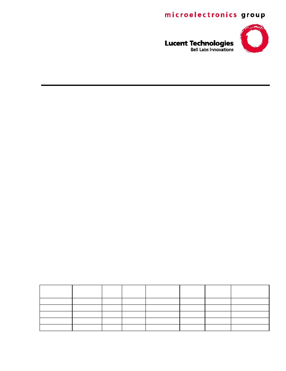
- Table 1 . ORCA Series 3 (3C and 3T) FPGAs
- Table 2 . ORCA Series 3 System Performance
- Table 3 . Look-Up Table Operating Modes
- Table 4 . Control Input Functionality
- Table 5 . Ripple Mode Equality Comparator Functions and Outputs
- Table 6 . SLIC Modes
- Table 7 . Configuration RAM Controlled Latch/ Flip-Flop Operation
- Table 8 . Inter-PLC Routing Resources
- Table 9 . PIO Options
- Table 10 . PIO Logic Options
- Table 11 . PIO Register Control Signals
- Table 12 . Readback Options
- Table 13 . Boundary-Scan Instructions
- Table 14 . Boundary-Scan ID Code
- Table 15 . TAP Controller Input/Outputs
- Table 16 . PowerPC/MPI Configuration
- Table 17 . i960/MPI Configuration
- Table 18 . MPI Internal Interface Signals
- Table 19 . MPI Setup and Control Registers
- Table 20 . MPI Setup and Control Registers Descriptions
- Table 21 . MPI Control Register 2
- Table 22 . Status Register
- Table 23 . Device ID Code
- Table 24 . Series 3 Family and Device ID Values
- Table 25 . ORCA Series 3 Device ID Descriptions
- Table 26 . PCM Registers
- Table 27 . DLL Mode Delay/1x Duty Cycle Programming Values
- Table 28 . DLL Mode Delay/2x Duty Cycle Programming Values
- Table 29 . PCM Oscillator Frequency Range 3Txxx
- Table 30 . PCM Oscillator Frequency Range 3Cxx
- Table 31 . PCM Control Registers
- Table 32 . Configuration Frame Format and Contents
- Table 33 . Configuration Frame Size
- Table 34 . Configuration Modes
- Table 35 . Absolute Maximum Ratings
- Table 36 . Recommended Operating Conditions
- Table 37 . Electrical Characteristics
- Table 38 . Derating for Commercial Devices (OR3Cxx)
- Table 39 . Derating for Industrial Devices (OR3Cxx)
- Table 40 . Derating for Commercial/Industrial Devices (OR3Txxx)
- Table 41 . Combinatorial PFU Timing Characteristics �
- Table 42 . Sequential PFU Timing Characteristics
- Table 43 . Ripple Mode PFU Timing Characteristics
- Table 44 . Synchronous Memory Write Characteristics
- Table 45 . Synchronous Memory Read Characteristics
- Table 46 . PFU Output MUX and Direct Routing Timing Characteristics
- Table 47 . Supplemental Logic and Interconnect Cell (SLIC) Timing Characteristics
- Table 48 . Programmable I/O (PIO) Timing Characteristics
- Table 49 . Microprocessor Interface (MPI) Timing Characteristics
- Table 50 . Programmable Clock Manager (PCM) Timing Characteristics (Preliminary Information)
- Table 51 . Boundary-Scan Timing Characteristics
- Table 52 . ExpressCLK (ECLK) and Fast Clock (FCLK) Timing Characteristics
- Table 53 . General-Purpose Clock Timing Characteristics (Internally Generated Clock)
- Table 54 . OR3Cxx ExpressCLK to Output Delay (Pin-to-Pin)
- Table 55 . OR3Cxx Fast Clock (FCLK) to Output Delay (Pin-to-Pin)
- Table 56 . OR3Cxx General System Clock (SCLK) to Output Delay (Pin-to-Pin)
- Table 57 . OR3C/Txxx Input to ExpressCLK (ECLK) Fast-Capture Setup/Hold Time (Pin-to-Pin)
- Table 58 . OR3C/Txxx Input to Fast Clock Setup/Hold Time (Pin-to-Pin)
- Table 59 . OR3C/Txxx Input to General System Clock (SCLK) Setup/Hold Time (Pin-to-Pin)
- Table 60 . General Configuration Mode Timing Characteristics
- Table 61 . Master Serial Configuration Mode Timing Characteristics
- Table 62 . Master Parallel Configuration Mode Timing Characteristics
- Table 63 . Asynchronous Peripheral Configuration Mode Timing Characteristics
- Table 64 . Slave Serial Configuration Mode Timing Characteristics
- Table 65 . Slave Parallel Configuration Mode Timing Characteristics
- Table 66 . Readback Timing Characteristics
- Table 67. Pin Descriptions�
- Table 68 . ORCA I/Os Summary
- Table 69 . Series 3 ExpressCLK Pins
- Table 70 . OR3T20, OR3T30, OR3C/T55, OR3C/T80, and OR3T125 208-Pin SQFP/SQFP2 Pinout
- Table 71. OR3T20, OR3T30, OR3C/T55, OR3C/T80, and OR3T125 240-Pin SQFP/SQFP2 Pinout
- Table 72. OR3T20, OR3T30, and OR3C/T55 256-Pin PBGA Pinout
- Table 73 . OR3T20, OR3T30, OR3C/T55, OR3C/T80, and OR3T125 352-Pin PBGA Pinout
- Table 74. OR3C/T80 and OR3T125 432-Pin EBGA Pinout
- Table 75. OR3T125 600-Pin EBGA Pinout
- Table 76 . Plastic Package Thermal Characteristics for the ORCA Series1
- Table 77 . Package Coplanarity
- Table 78 . Package Parasitics
- Table 79 . Voltage Options
- Table 80 . Temperature Options
- Table 81 . Package Options
- Table 82 . ORCA Series 3 Package Matrix
- Table 83 . Speed Grade Options
- List of Figures
- Figure 1 . OR3C/T55 Array
- Figure 2 . PFU Ports
- Figure 3 . Simplified PFU Diagram
- Figure 4 . Simplified F4 and F5 Logic Modes
- Figure 5 . Softwired LUT Topology Examples
- Figure 6 . Ripple Mode
- Figure 7 . Counter Submode
- Figure 8 . Multiplier Submode
- Figure 9 . Memory Mode
- Figure 10 . Memory Mode Expansion ExampleÑ128 x 8 RAM
- Figure 11 . SLIC All Modes Diagram
- Figure 12 . Buffer Mode
- Figure 13 . Buffer-Buffer-Decoder Mode
- Figure 14 . Buffer-Decoder-Buffer Mode
- Figure 15 . Buffer-Decoder-Decoder Mode
- Figure 16 . Decoder Mode
- Figure 17 . Latch/FF Set/Reset Configurations
- Figure 18 . Configurable Interconnect Point
- Figure 19 . Single PLC View of Inter-PLC Route Segments
- Figure 20 . Multiple PLC View of Inter-PLC Routing
- Figure 21 . PLC Architecture
- Figure 22 . OR3C/Txxx Programmable Input/Output (PIO) Image from ORCA Foundry
- Figure 23 . Fast-Capture Latch and Timing
- Figure 24 . PIO Input Demultiplexing
- Figure 25 . Output Multiplexing (OUT1OUT2 Mode)
- Figure 26 . Output Multiplexing (OUT2OUTREG Mode)
- Figure 27 . PIC Architecture
- Figure 28 . Interquad Routing
- Figure 29 . hIQ Block Detail
- Figure 30 . Top (TMID) Routing
- Figure 31 . PFU Clock Sources
- Figure 32 . ORCA Series 3 System Clock Distribution Overview
- Figure 33 . PIC System Clock Spine Generation
- Figure 34 . ExpressCLK and Fast Clock Distribution
- Figure 35 . Top CLKCNTRL Function Block
- Figure 36 . Printed-Circuit Board with Boundary- Scan Circuitry
- Figure 37 . Boundary-Scan Interface
- Figure 38 . ORCA Series Boundary-Scan Circuitry Functional Diagram
- Figure 39 . TAP Controller State Transition Diagram
- Figure 40 . Boundary-Scan Cell
- Figure 41 . Instruction Register Scan Timing Diagram
- Figure 42 . MPI Block Diagram
- Figure 43 . PowerPC/MPI
- Figure 44 . i960/MPI
- Figure 45 . PCM Block Diagram
- Figure 46 . PCM Functional Block Diagram
- Figure 47 . ExpressCLK Delay Minimization Using the PCM
- Figure 48 . Clock Phase Adjustment Using the PCM
- Figure 49 . FPGA States of Operation
- Figure 50 . Initialization/Configuration/Start-Up Waveforms
- Figure 51 . Start-Up Waveforms
- Figure 52 . Serial Configuration Data FormatÑAutoincrement Mode
- Figure 53 . Serial Configuration Data FormatÑExplicit Mode
- Figure 54 . Master Parallel Configuration Schematic
- Figure 55 . Master Serial Configuration Schematic
- Figure 56 . Asynchronous Peripheral Configuration
- Figure 57 . PowerPC/MPI Configuration Schematic
- Figure 58 . i960/MPI Configuration Schematic
- Figure 59 . Configuration Through MPI
- Figure 60 . Readback Through MPI
- Figure 61 . Slave Serial Configuration Schematic
- Figure 62 . Slave Parallel Configuration Schematic
- Figure 63 . Daisy-Chain Configuration Schematic
- Figure 64 . Combinatorial PFU Timing
- Figure 65 . Synchronous Memory Write Characteristics
- Figure 66 . Synchronous Memory Read Cycle
- Figure 67 . MPI PowerPC User Space Read Timing
- Figure 68 . MPI PowerPC User Space Write Timing
- Figure 69 . MPI PowerPC Internal Read Timing
- Figure 70 . MPI PowerPC Internal Write Timing
- Figure 71 . MPI i960 User Space Read Timing
- Figure 72 . MPI i960 User Space Write Timing
- Figure 73 . MPI i960 Internal Read Timing
- Figure 74 . MPI i960 Internal Write Timing
- Figure 75 . Boundary-Scan Timing Diagram
- Figure 76 . ExpressCLK to Output Delay
- Figure 77 . Fast Clock to Output Delay
- Figure 78 . System Clock to Output Delay
- Figure 79 . Input to ExpressCLK Setup/Hold Time
- Figure 80 . Input to Fast Clock Setup/Hold Time
- Figure 81 . Input to System Clock Setup/Hold Time
- Figure 82 . General Configuration Mode Timing Diagram
- Figure 83 . Master Serial Configuration Mode Timing Diagram
- Figure 84 . Master Parallel Configuration Mode Timing Diagram
- Figure 85 . Asynchronous Peripheral Configuration Mode Timing Diagram
- Figure 86 . Slave Serial Configuration Mode Timing Diagram
- Figure 87 . Slave Parallel Configuration Mode Timing Diagram
- Figure 88 . Readback Timing Diagram
- Figure 89 . ac Test Loads
- Figure 90 . Output Buffer Delays
- Figure 91 . Input Buffer Delays
- Figure 92 . Sinklim (TJ = 25 ∞C, VDD = 5.0 V)
- Figure 93 . Slewlim (TJ = 25 ∞C, VDD = 5.0 V)
- Figure 94 . Fast (TJ = 25 ∞C, VDD = 5.0 V)
- Figure 95 . Sinklim (TJ = 125 ∞C, VDD = 4.5 V)
- Figure 96 . Slewlim (TJ = 125 ∞C, VDD = 4.5 V)
- Figure 97 . Fast (TJ = 125 ∞C, VDD = 4.5 V)
- Figure 98 . Sinklim (TJ = 25 ∞C, VDD = 3.3 V)
- Figure 99 . Slewlim (TJ = 25 ∞C, VDD = 3.3 V)
- Figure 100 . Fast (TJ = 25 ∞C, VDD = 3.3 V)
- Figure 101 . Sinklim (TJ = 125 ∞C, VDD = 3.0 V)
- Figure 102 . Slewlim (TJ = 125 ∞C, VDD = 3.0 V)
- Figure 103 . Fast (TJ = 125 ∞C, VDD = 3.0 V)
- Figure 104 . Package Parasitics
- Contact Us
Data Sheet
June 1999
ORCA
Æ
Series 3C and 3T
Field-Programmable Gate Arrays
Features
s
High-performance, cost-effective, 0.35 µm (OR3C) and
0.3 µm (OR3T) 4-level metal technology, (4- or 5-input
look-up table delay of 1.1 ns with -7 speed grade in
0.3 µm).
s
Same basic architecture as lower-voltage, advanced
process technology Series 3 architectures. (See
ORCA
Series 3L FPGA documentation.)
s
Up to 186,000 usable gates.
s
Up to 452 user I/Os. (OR3Txxx I/Os are 5 V tolerant to
allow interconnection to both 3.3 V and 5 V devices,
selectable on a per-pin basis.)
s
Pin selectable I/O clamping diodes provide 5 V or 3.3 V
PCI compliance and 5 V tolerance on OR3Txxx devices.
s
Twin-quad programmable function unit (PFU) architec-
ture with eight 16-bit look-up tables (LUTs) per PFU,
organized in two nibbles for use in nibble- or byte-wide
functions. Allows for mixed arithmetic and logic functions
in a single PFU.
s
Nine user registers per PFU, one following each LUT,
plus one extra. All have programmable clock enable and
local set/reset, plus a global set/reset that can be dis-
abled per PFU.
s
Flexible input structure (FINS) of the PFUs provides a
routability enhancement for LUTs with shared inputs and
the logic flexibility of LUTs with independent inputs.
s
Fast-carry logic and routing to adjacent PFUs for nibble-,
byte-wide, or longer arithmetic functions, with the option
to register the PFU carry-out.
s
Softwired LUTs (SWL) allow fast cascading of up to
three levels of LUT logic in a single PFU for up to 40%
speed improvement.
s
Supplemental logic and interconnect cell (SLIC) provides
3-statable buffers, up to 10-bit decoder, and
PAL*-like
AND-OR with optional INVERT in each programmable
logic cell (PLC), with over 50% speed improvement typi-
cal.
s
Abundant hierarchical routing resources based on rout-
ing two data nibbles and two control lines per set provide
for faster place and route implementations and less rout-
ing delay.
s
TTL or CMOS input levels programmable per pin for the
OR3Cxx (5.0 V) devices.
s
Individually programmable drive capability:
12 mA sink/6 mA source or 6 mA sink/3 mA source.
s
Built-in boundary scan (
IEEE
1149.1 JTAG) and
TS_ALL testability function to 3-state all I/O pins.
s
Enhanced system clock routing for low skew, high-speed
clocks originating on-chip or at any I/O.
s
Up to four ExpressCLK inputs allow extremely fast clock-
ing of signals on- and off-chip plus access to internal
general clock routing.
s
StopCLK feature to glitchlessly stop/start ExpressCLKs
independently by user command.
s
Programmable I/O (PIO) has:
-- Fast-capture input latch and input flip-flop (FF) latch
for reduced input setup time and zero hold time.
-- Capability to (de)multiplex I/O signals.
-- Fast access to SLIC for decodes and
PAL-like
functions.
-- Output FF and two-signal function generator to
reduce CLK to output propagation delay.
-- Fast open-drain dive capability
-- Capability to register 3-state enable signal.
s
Baseline FPGA family used in Series 3+ FPSCs (field
programmable system chips) which combine FPGA logic
and standard cell logic on one device.
*
PAL
is a trademark of Advanced Micro Devices, Inc.
IEEE
is a registered trademark of The Institute of Electrical and
Electronics Engineers, Inc.
Table 1.
ORCA
Series 3 (3C and 3T) FPGAs
The system gate counts range from a logic-only gate count to a gate count assuming 30% of the PFUs/SLICs being used as RAMs.
The logic-only gate count includes each PFU/SLIC (counted as 108 gates per PFU/SLIC), including 12 gates per LUT/FF pair (eight per
PFU), and 12 gates per SLIC/FF pair (one per PFU). Each of the four PIOs per PIC is counted as 16 gates (two FFs, fast-capture latch,
output logic, CLK drivers, and I/O buffers). PFUs used as RAM are counted at four gates per bit, with each PFU capable of implementing
a 32 x 4 RAM (or 512 gates) per PFU.
Device
System
Gates
LUTs
Registers
Max User RAM
User I/Os
Array Size
Process
Technology
OR3T20
36K
1152
1872
18K
196
12 x 12
0.3 µm/4 LM
OR3T30
48K
1568
2436
25K
228
14 x 14
0.3 µm/4 LM
OR3C/3T55
80K
2592
3780
42K
292
18 x 18
0.3 µm/4 LM
OR3C/3T80
116K
3872
5412
62K
356
22 x 22
0.3 µm/4 LM
OR3T125
186K
6272
8400
100K
452
28 x 28
0.3 µm/4 LM

Table of Contents
Contents
Page
Contents
Page
2
Lucent Technologies Inc.
Data Sheet
June 1999
ORCA Series 3C and 3T FPGAs
Features ......................................................................1
System-Level Features................................................6
Description...................................................................7
FPGA Overview ........................................................7
PLC Logic ..................................................................7
PIC Logic ...................................................................8
System Features .......................................................8
Routing ......................................................................8
Configuration .............................................................8
ORCA
Foundry Development System ......................9
Architecture .................................................................9
Programmable Logic Cells ........................................11
Programmable Function Unit ..................................11
Look-Up Table Operating Modes ............................13
Supplemental Logic and Interconnect Cell (SLIC) ..21
PLC Latches/Flip-Flops ...........................................25
PLC Routing Resources ..........................................27
PLC Architectural Description .................................34
Programmable Input/Output Cells .............................36
5 V Tolerant I/O .......................................................37
PCI Compliant I/O ...................................................37
Inputs ......................................................................38
Outputs ....................................................................41
PIC Routing Resources ...........................................44
PIC Architectural Description ..................................45
High-Level Routing Resources..................................47
Interquad Routing ....................................................47
Programmable Corner Cell Routing ........................48
PIC Interquad (MID) Routing ...................................49
Clock Distribution Network ........................................50
PFU Clock Sources .................................................50
Clock Distribution in the PLC Array .........................51
Clock Sources to the PLC Array .............................52
Clocks in the PICs ...................................................52
ExpressCLK Inputs .................................................53
Selecting Clock Input Pins ......................................53
Special Function Blocks ............................................54
Single Function Blocks ............................................54
Boundary Scan ........................................................57
Microprocessor Interface (MPI) .................................64
PowerPC
System ....................................................65
i960
System ............................................................66
MPI Interface to FPGA ............................................67
MPI Setup and Control ............................................68
Programmable Clock Manager (PCM) ......................72
PCM Registers ........................................................73
Delay-Locked Loop (DLL) Mode .............................75
Phase-Locked Loop (PLL) Mode ............................76
PCM/FPGA Internal Interface .................................79
PCM Operation .......................................................79
PCM Detailed Programming ...................................80
PCM Applications ....................................................83
PCM Cautions ........................................................ 84
FPGA States of Operation ........................................ 85
Initialization ............................................................. 85
Configuration .......................................................... 86
Start-Up .................................................................. 87
Reconfiguration ...................................................... 88
Partial Reconfiguration ........................................... 88
Other Configuration Options ................................... 88
Configuration Data Format ...................................... 89
Using
ORCA
Foundry to Generate
Configuration RAM Data ....................................... 89
Configuration Data Frame ...................................... 89
Bit Stream Error Checking ...................................... 91
FPGA Configuration Modes...................................... 92
Master Parallel Mode ............................................. 92
Master Serial Mode ................................................ 93
Asynchronous Peripheral Mode ............................. 94
Microprocessor Interface (MPI) Mode .................... 94
Slave Serial Mode .................................................. 97
Slave Parallel Mode ............................................... 97
Daisy-Chaining ....................................................... 98
Daisy-Chaining with Boundary Scan ...................... 99
Absolute Maximum Ratings.................................... 100
Recommended Operating Conditions .................. 100
Electrical Characteristics ........................................ 101
Timing Characteristics ............................................ 103
Description ........................................................... 103
PFU Timing ......................................................... 104
PLC Timing ........................................................... 111
SLIC Timing .......................................................... 111
PIO Timing ........................................................... 112
Special Function Blocks Timing ........................... 115
Clock Timing ......................................................... 123
Configuration Timing ............................................ 133
Readback Timing ................................................. 142
Input/Output Buffer Measurement Conditions ........ 143
Output Buffer Characteristics ................................. 144
OR3Cxx ................................................................ 144
OR3Txxx .............................................................. 145
Estimating Power Dissipation ................................. 146
OR3Cxx ................................................................ 146
OR3Txxx (Preliminary Information) ...................... 147
Pin Information ....................................................... 149
Pin Descriptions ................................................... 149
Package Compatibility .......................................... 153
Compatibility with OR2C/TxxA Series .................. 154
Package Thermal Characteristics........................... 194
JA ....................................................................... 194
JC ...................................................................... 194
JC ...................................................................... 194
JB ...................................................................... 194
FPGA Maximum Junction Temperature ............... 195

Table of Contents
Contents
Page
Contents
Page
Lucent Technologies Inc.
3
ORCA Series 3C and 3T FPGAs
June 1999
Data Sheet
Package Coplanarity ...............................................196
Package Parasitics ..................................................196
Package Outline Diagrams......................................197
Terms and Definitions ...........................................197
208-Pin SQFP .......................................................198
208-Pin SQFP2 .....................................................199
240-Pin SQFP .......................................................200
240-Pin SQFP2 .....................................................201
256-Pin PBGA .......................................................202
352-Pin PBGA .......................................................203
432-Pin EBGA .......................................................204
600-Pin EBGA .......................................................205
Ordering Information................................................206
Index........................................................................207
Tables
Table 1.
ORCA
Series 3 (3C and 3T) FPGAs ............ 2
Table 2.
ORCA
Series 3 System Performance .......... 6
Table 3. Look-Up Table Operating Modes ............... 13
Table 4. Control Input Functionality .......................... 14
Table 5. Ripple Mode Equality Comparator
Functions and Outputs ............................................ 18
Table 6. SLIC Modes ................................................ 21
Table 7. Configuration RAM Controlled
Latch/Flip-Flop Operation ........................................ 25
Table 8. Inter-PLC Routing Resources ..................... 31
Table 9. PIO Options ................................................ 37
Table 10. PIO Logic Options .................................... 43
Table 11. PIO Register Control Signals .................... 43
Table 12. Readback Options .................................... 54
Table 13. Boundary-Scan Instructions ..................... 58
Table 14. Boundary-Scan ID Code ........................... 59
Table 15. TAP Controller Input/Outputs ................... 61
Table 16.
PowerPC
/MPI Configuration ..................... 65
Table 17.
i960
/MPI Configuration ............................. 66
Table 18. MPI Internal Interface Signals .................. 67
Table 19. MPI Setup and Control Registers ............. 68
Table 20. MPI Setup and Control Registers
Description ............................................................... 68
Table 21. MPI Control Register 2 ............................. 69
Table 22. Status Register ......................................... 70
Table 23. Device ID Code ........................................ 71
Table 24. Series 3 Family and Device ID Values ..... 71
Table 25.
ORCA
Series 3 Device ID Descriptions .... 71
Table 26. PCM Registers ......................................... 73
Table 27. DLL Mode Delay/1x Duty Cycle
Programming Values ............................................... 75
Table 28. DLL Mode Delay/2x Duty Cycle
Programming Values ............................................... 76
Table 29. PCM Oscillator Frequency Range 3Txxx . 78
Table 30. PCM Oscillator Frequency Range 3Cxx ... 78
Table 31. PCM Control Registers ............................. 80
Table 32. Configuration Frame Format and
Contents .................................................................. 90
Table 33. Configuration Frame Size ......................... 91
Table 34. Configuration Modes ................................ 92
Table 35. Absolute Maximum Ratings .................... 100
Table 36. Recommended Operating Conditions .... 100
Table 37. Electrical Characteristics ........................ 101
Table 38. Derating for Commercial Devices
(OR3Cxx) .............................................................. 103
Table 39. Derating for Industrial Devices (OR3Cxx) 103
Table 40. Derating for Commercial/Industrial
Devices (OR3Txxx) ............................................... 103
Table 41. Combinatorial PFU Timing
Characteristics ....................................................... 104
Table 42. Sequential PFU Timing Characteristics .. 106
Table 43. Ripple Mode PFU Timing
Characteristics ....................................................... 107
Table 44. Synchronous Memory Write
Characteristics ....................................................... 109
Table 45. Synchronous Memory Read
Characteristics ....................................................... 110
Table 46. PFU Output MUX and Direct Routing
Timing Characteristics ........................................... 111
Table 47. Supplemental Logic and Interconnect
Cell (SLIC) Timing Characteristics ........................ 111
Table 48. Programmable I/O (PIO) Timing
Characteristics ....................................................... 112
Table 49. Microprocessor Interface (MPI) Timing
Characteristics ....................................................... 115
Table 50. Programmable Clock Manager (PCM)
Timing Characteristics (Preliminary Information) .. 121
Table 51. Boundary-Scan Timing Characteristics .. 122
Table 52. ExpressCLK (ECLK) and Fast Clock
(FCLK) Timing Characteristics .............................. 123
Table 53. General-Purpose Clock Timing
Characteristics (Internally Generated Clock) .........124
Table 54. OR3Cxx ExpressCLK to Output Delay
(Pin-to-Pin) ............................................................ 125
Table 55. OR3Cxx Fast Clock (FCLK) to Output
Delay (Pin-to-Pin) .................................................. 126
Table 56. OR3Cxx General System Clock (SCLK)
to Output Delay (Pin-to-Pin) .................................. 127
Table 57. OR3C/Txxx Input to ExpressCLK (ECLK)
Fast-Capture Setup/Hold Time (Pin-to-Pin) .......... 128
Table 58. OR3C/Txxx Input to Fast Clock
Setup/Hold Time (Pin-to-Pin) ................................ 130
Table 59. OR3C/Txxx Input to General System
Clock (SCLK) Setup/Hold Time (Pin-to-Pin) .......... 132
Table 60. General Configuration Mode Timing
Characteristics ....................................................... 133
Table 61. Master Serial Configuration Mode Timing

Table of Contents
Contents
Page
Contents
Page
4
Lucent Technologies Inc.
Data Sheet
June 1999
ORCA Series 3C and 3T FPGAs
Characteristics ...................................................... 136
Table 62. Master Parallel Configuration Mode Timing
Characteristics ...................................................... 137
Table 63. Asynchronous Peripheral Configuration Mode
Timing Characteristics ........................................... 138
Table 64. Slave Serial Configuration Mode Timing
Characteristics ...................................................... 139
Table 65. Slave Parallel Configuration Mode
Timing Characteristics ........................................... 140
Table 66. Readback Timing Characteristics ........... 142
Table 67. Pin Descriptions ...................................... 149
Table 68.
ORCA
I/Os Summary ............................. 153
Table 69. Series 3 ExpressCLK Pins ..................... 154
Table 70. OR3T20, OR3T30, OR3C/T55,
OR3C/T80, and OR3T125 208-Pin
SQFP/SQFP2 Pinout ............................................ 155
Table 71. OR3T20, OR3T30, OR3C/T55,
OR3C/T80, and OR3T125 240-Pin
SQFP/SQFP2 Pinout ............................................ 161
Table 72. OR3T20, OR3T30, and OR3C/T55
256-Pin PBGA Pinout ............................................ 168
Table 73. OR3T20, OR3T30, OR3C/T55,
OR3C/T80, and OR3T125 352-Pin PBGA Pinout . 172
Table 74. OR3C/T80 and OR3T125 432-Pin
EBGA Pinout ......................................................... 182
Table 75. OR3T125 600-Pin EBGA Pinout ............ 187
Table 76. Plastic Package Thermal
Characteristics for the
ORCA
Series ..................... 195
Table 77. Package Coplanarity .............................. 196
Table 78. Package Parasitics ................................. 196
Table 79. Voltage Options ...................................... 206
Table 80. Temperature Options ............................. 206
Table 81. Package Options .................................... 206
Table 82.
ORCA
Series 3 Package Matrix ............. 206
Table 83. Speed Grade Options ............................. 206
Figures
Figure 1. OR3C/T55 Array ........................................ 10
Figure 2. PFU Ports .................................................. 11
Figure 3. Simplified PFU Diagram ............................ 12
Figure 4. Simplified F4 and F5 Logic Modes ............ 14
Figure 5. Softwired LUT Topology Examples ........... 15
Figure 6. Ripple Mode .............................................. 16
Figure 7. Counter Submode ..................................... 17
Figure 8. Multiplier Submode .................................... 18
Figure 9. Memory Mode ........................................... 19
Figure 10. Memory Mode Expansion Example--
128 x 8 RAM ........................................................... 20
Figure 11. SLIC All Modes Diagram ......................... 22
Figure 12. Buffer Mode ............................................. 22
Figure 13. Buffer-Buffer-Decoder Mode ................... 23
Figure 14. Buffer-Decoder-Buffer Mode ................... 23
Figure 15. Buffer-Decoder-Decoder Mode ............... 24
Figure 16. Decoder Mode ......................................... 24
Figure 17. Latch/FF Set/Reset Configurations ......... 26
Figure 18. Configurable Interconnect Point .............. 27
Figure 19. Single PLC View of Inter-PLC Route
Segments ................................................................ 28
Figure 20. Multiple PLC View of Inter-PLC Routing . 32
Figure 21. PLC Architecture .....................................35
Figure 22. OR3C/Txxx Programmable Input/Output
(PIO) Image from
ORCA
Foundry ........................... 36
Figure 23. Fast-Capture Latch and Timing ............... 39
Figure 24. PIO Input Demultiplexing ......................... 40
Figure 25. Output Multiplexing (OUT1OUT2 Mode) . 42
Figure 26. Output Multiplexing
(OUT2OUTREG Mode) ........................................... 42
Figure 27. PIC Architecture ...................................... 46
Figure 28. Interquad Routing .................................... 47
Figure 29. hIQ Block Detail ....................................... 48
Figure 30. Top (TMID) Routing ................................. 49
Figure 31. PFU Clock Sources ................................. 50
Figure 32.
ORCA
Series 3 System Clock
Distribution Overview .............................................. 51
Figure 33. PIC System Clock Spine Generation ...... 52
Figure 34. ExpressCLK and Fast Clock Distribution 53
Figure 35. Top CLKCNTRL Function Block .............. 56
Figure 36. Printed-Circuit Board with Boundary-
Scan Circuitry .......................................................... 57
Figure 37. Boundary-Scan Interface ......................... 58
Figure 38.
ORCA
Series Boundary-Scan Circuitry
Functional Diagram ................................................. 60
Figure 39. TAP Controller State Transition Diagram 61
Figure 40. Boundary-Scan Cell ................................ 62
Figure 41. Instruction Register Scan Timing
Diagram ................................................................... 63
Figure 42. MPI Block Diagram .................................. 64
Figure 43.
PowerPC
/MPI .......................................... 65
Figure 44.
i960
/MPI ..................................................66
Figure 45. PCM Block Diagram ................................ 72
Figure 46. PCM Functional Block Diagram .............. 74
Figure 47. ExpressCLK Delay Minimization Using
the PCM .................................................................. 76
Figure 48. Clock Phase Adjustment Using the PCM 83
Figure 49. FPGA States of Operation ....................... 85
Figure 50. Initialization/Configuration/Start-Up
Waveforms .............................................................. 86
Figure 51. Start-Up Waveforms ................................ 88
Figure 52. Serial Configuration Data Format--
Autoincrement Mode ............................................... 90
Figure 53. Serial Configuration Data Format--

Table of Contents
Contents
Page
Contents
Page
Lucent Technologies Inc.
5
ORCA Series 3C and 3T FPGAs
June 1999
Data Sheet
Explicit Mode ........................................................... 90
Figure 54. Master Parallel Configuration Schematic 92
Figure 55. Master Serial Configuration Schematic ... 93
Figure 56. Asynchronous Peripheral Configuration .. 94
Figure 57.
PowerPC
/MPI Configuration Schematic .. 95
Figure 58.
i960
/MPI Configuration Schematic .......... 95
Figure 59. Configuration Through MPI ..................... 95
Figure 60. Readback Through MPI .......................... 96
Figure 61. Slave Serial Configuration Schematic ..... 97
Figure 62. Slave Parallel Configuration Schematic .. 97
Figure 63. Daisy-Chain Configuration Schematic ..... 98
Figure 64. Combinatorial PFU Timing .................... 105
Figure 65. Synchronous Memory Write
Characteristics ...................................................... 109
Figure 66. Synchronous Memory Read Cycle ........ 110
Figure 67. MPI
PowerPC
User Space Read Timing 117
Figure 68. MPI
PowerPC
User Space Write Timing 117
Figure 69. MPI
PowerPC
Internal Read Timing ..... 118
Figure 70. MPI
PowerPC
Internal Write Timing ...... 118
Figure 71. MPI
i960
User Space Read Timing ....... 119
Figure 72. MPI
i960
User Space Write Timing ....... 119
Figure 73. MPI
i960
Internal Read Timing .............. 120
Figure 74. MPI
i960
Internal Write Timing .............. 120
Figure 75. Boundary-Scan Timing Diagram ........... 122
Figure 76. ExpressCLK to Output Delay ................ 125
Figure 77. Fast Clock to Output Delay ................... 126
Figure 78. System Clock to Output Delay .............. 127
Figure 79. Input to ExpressCLK Setup/Hold Time .. 129
Figure 80. Input to Fast Clock Setup/Hold Time ..... 131
Figure 81. Input to System Clock Setup/Hold Time 132
Figure 82. General Configuration Mode Timing
Diagram ................................................................. 135
Figure 83. Master Serial Configuration Mode
Timing Diagram ..................................................... 136
Figure 84. Master Parallel Configuration Mode
Timing Diagram ..................................................... 137
Figure 85. Asynchronous Peripheral Configuration
Mode Timing Diagram ........................................... 138
Figure 86. Slave Serial Configuration Mode
Timing Diagram ..................................................... 139
Figure 87. Slave Parallel Configuration Mode
Timing Diagram ..................................................... 140
Figure 88. Readback Timing Diagram .................... 142
Figure 89. ac Test Loads ........................................ 143
Figure 90. Output Buffer Delays .............................143
Figure 91. Input Buffer Delays ................................ 143
Figure 92. Sinklim (T
J
= 25 ∞C, V
DD
= 5.0 V) .......... 144
Figure 93. Slewlim (T
J
= 25 ∞C, V
DD
= 5.0 V) .........144
Figure 94. Fast (T
J
∞C, V
DD
= 5.0 V) ......................144
Figure 95. Sinklim (T
J
= 125 ∞C, V
DD
= 4.5 V) ........ 144
Figure 96. Slewlim (T
J
= 125 ∞C, V
DD
= 4.5 V) ....... 144
Figure 97. Fast (T
J
= 125 ∞C, V
DD
= 4.5 V) ............ 144
Figure 98. Sinklim (T
J
= 25 ∞C, V
DD
= 3.3 V) .......... 145
Figure 99. Slewlim (T
J
= 25 ∞C, V
DD
= 3.3 V) .........145
Figure 100. Fast (T
J
= 25 ∞C, V
DD
= 3.3 V) ............ 145
Figure 101. Sinklim (T
J
= 125 ∞C, V
DD
= 3.0 V) ...... 145
Figure 102. Slewlim (T
J
= 125 ∞C, V
DD
= 3.0 V) ..... 145
Figure 103. Fast (T
J
= 125 ∞C, V
DD
= 3.0 V) .......... 145
Figure 104. Package Parasitics .............................. 196

6
6
Lucent Technologies Inc.
Data Sheet
June 1999
ORCA Series 3C and 3T FPGAs
System-Level Features
System-level features reduce glue logic requirements
and make a system on a chip possible. These features
in the
ORCA
Series 3 include:
s
Full PCI local bus compliance.
s
Dual-use microprocessor interface (MPI) can be
used for configuration, readback, device control, and
device status, as well as for a general-purpose inter-
face to the FPGA. Glueless interface to
i960
* and
PowerPC
processors with user-configurable
address space provided.
s
Parallel readback of configuration data capability with
the built-in microprocessor interface.
s
Programmable clock manager (PCM) adjusts clock
phase and duty cycle for input clock rates from
5 MHz to 120 MHz. The PCM may be combined with
FPGA logic to create complex functions, such as dig-
ital phase-locked loops (DPLL), frequency counters,
and frequency synthesizers or clock doublers. Two
PCMs are provided per device.
s
True, internal, 3-state, bidirectional buses with simple
control provided by the SLIC.
s
32 x 4 RAM per PFU, configurable as single- or dual-
port at >176 MHz. Create large, fast RAM/ROM
blocks (128 x 8 in only eight PFUs) using the SLIC
decoders as bank drivers.
*
i960
is a registered trademark of Intel Corporation.
PowerPC
is a registered trademark of International Business
Machines Corporation.
Table 2.
ORCA
Series 3 System Performance
1. Implemented using 8 x 1 multiplier mode (unpipelined), register-to-register, two 8-bit inputs, one 16-bit output.
2. Implemented using two 32 x 12 ROMs and one 12-bit adder, one 8-bit input, one fixed operand, one 16-bit output.
3. Implemented using 8 x 1 multiplier mode (fully pipelined), two 8-bit inputs, one 16-bit output (7 of 15 PFUs contain only pipelining registers).
4. Implemented using 32 x 4 RAM mode with read data on 3-state buffer to bidirectional read/write bus.
5. Implemented using 32 x 4 dual-port RAM mode.
6. Implemented in one partially occupied SLIC with decoded output set up to CE in same PLC.
7. Implemented in five partially occupied SLICs.
Parameter
# PFUs
Speed
Unit
-4
-5
-6
-7
16-bit Loadable Up/Down Counter
2
78
102
131
168
MHz
16-bit Accumulator
2
78
102
131
168
MHz
8 x 8 Parallel Multiplier:
Multiplier Mode, Unpipelined
1
ROM Mode, Unpipelined
2
Multiplier Mode, Pipelined
3
11.5
8
15
19
51
76
25
66
104
30
80
127
38
102
166
MHz
MHz
MHz
32 x 16 RAM (synchronous):
Single-port, 3-state Bus
4
Dual-port
5
4
4
97
127
127
166
151
203
192
253
MHz
MHz
128 x 8 RAM (synchronous):
Single-port, 3-state Bus
4
Dual-port
5
8
8
88
88
116
116
139
139
176
176
MHz
MHz
8-bit Address Decode (internal):
Using Softwired LUTs
Using SLICs
6
0.25
0
4.87
2.35
3.66
1.82
2.58
1.23
2.03
0.99
ns
ns
32-bit Address Decode (internal):
Using Softwired LUTs
Using SLICs
7
2
0
16.06
6.91
12.07
5.41
9.01
4.21
7.03
3.37
ns
ns
36-bit Parity Check (internal)
2
16.06
12.07
9.01
7.03
ns

Lucent Technologies Inc.
7
Data Sheet
June 1999
ORCA Series 3C and 3T FPGAs
Description
FPGA Overview
The
ORCA
Series 3 FPGAs are a new generation of
SRAM-based FPGAs built on the successful OR2C/
TxxA FPGA Series from Lucent Technologies Micro-
electronics Group, with enhancements and innovations
geared toward today's high-speed designs and tomor-
row's systems on a single chip. Designed from the start
to be synthesis friendly and to reduce place and route
times while maintaining the complete routability of the
ORCA
2C/2T devices, Series 3 more than doubles the
logic available in each logic block and incorporates sys-
tem-level features that can further reduce logic require-
ments and increase system speed.
ORCA
Series 3
devices contain many new patented enhancements
and are offered in a variety of packages, speed grades,
and temperature ranges.
The
ORCA
Series 3 FPGAs consist of three basic ele-
ments: programmable logic cells (PLCs), programma-
ble input/output cells (PICs), and system-level features.
An array of PLCs is surrounded by PICs. Each PLC
contains a programmable function unit (PFU), a sup-
plemental logic and interconnect cell (SLIC), local rout-
ing resources, and configuration RAM. Most of the
FPGA logic is performed in the PFU, but decoders,
PAL
-like functions, and 3-state buffering can be per-
formed in the SLIC. The PICs provide device inputs
and outputs and can be used to register signals and to
perform input demultiplexing, output multiplexing, and
other functions on two output signals. Some of the sys-
tem-level functions include the new microprocessor
interface (MPI) and the programmable clock manager
(PCM).
PLC Logic
Each PFU within a PLC contains eight 4-input (16-bit)
look-up tables (LUTs), eight latches/flip-flops (FFs),
and one additional flip-flop that may be used indepen-
dently or with arithmetic functions.
The PFU is organized in a twin-quad fashion: two sets
of four LUTs and FFs that can be controlled indepen-
dently. LUTs may also be combined for use in arith-
metic functions using fast-carry chain logic in either
4-bit or 8-bit modes. The carry-out of either mode may
be registered in the ninth FF for pipelining. Each PFU
may also be configured as a synchronous 32 x 4 sin-
gle- or dual-port RAM or ROM. The FFs (or latches)
may obtain input from LUT outputs or directly from
invertible PFU inputs, or they can be tied high or tied
low. The FFs also have programmable clock polarity,
clock enables, and local set/reset.
The SLIC is connected to PLC routing resources and to
the outputs of the PFU. It contains 3-state, bidirectional
buffers and logic to perform up to a 10-bit AND function
for decoding, or an AND-OR with optional INVERT
(AOI) to perform
PAL
-like functions. The 3-state drivers
in the SLIC and their direct connections to the PFU out-
puts make fast, true 3-state buses possible within the
FPGA, reducing required routing and allowing for real-
world system performance.

8
8
Lucent Technologies Inc.
Data Sheet
June 1999
ORCA Series 3C and 3T FPGAs
Description
(continued)
PIC Logic
Series 3 PIC addresses the demand for ever-increas-
ing system clock speeds. Each PIC contains four pro-
grammable inputs/outputs (PIOs) and routing
resources. On the input side, each PIO contains a fast-
capture latch that is clocked by an ExpressCLK. This
latch is followed by a latch/FF that is clocked by a sys-
tem clock from the internal general clock routing. The
combination provides for very low setup requirements
and zero hold times for signals coming on-chip. It may
also be used to demultiplex an input signal, such as a
multiplexed address/data signal, and register the sig-
nals without explicitly building a demultiplexer. Two
input signals are available to the PLC array from each
PIO, and the
ORCA
2C/2T capability to use any input
pin as a clock or other global input is maintained.
On the output side of each PIO, two outputs from the
PLC array can be routed to each output flip-flop, and
logic can be associated with each I/O pad. The output
logic associated with each pad allows for multiplexing
of output signals and other functions of two output sig-
nals.
The output FF in combination with output signal multi-
plexing, is particularly useful for registering address
signals to be multiplexed with data, allowing a full clock
cycle for the data to propagate to the output. The I/O
buffer associated with each pad is very similar to the
ORCA
2C/2T Series buffer with a new, fast, open-drain
option for ease of use on system buses.
System Features
Series 3 also provides system-level functionality by
means of its dual-use microprocessor interface and its
innovative programmable clock manager. These func-
tional blocks allow for easy glueless system interfacing
and the capability to adjust to varying conditions in
today's high-speed systems.
Routing
The abundant routing resources of the
ORCA
Series 3
FPGAs are organized to route signals individually or as
buses with related control signals. Clocks are routed on
a low-skew, high-speed distribution network and may
be sourced from PLC logic, externally from any I/O
pad, or from the very fast ExpressCLK pins. Express-
CLKs may be glitchlessly and independently enabled
and disabled with a programmable control signal using
the new StopCLK feature. The improved PIC routing
resources are now similar to the patented intra-PLC
routing resources and provide great flexibility in moving
signals to and from the PIOs. This flexibility translates
into an improved capability to route designs at the
required speeds when the I/O signals have been locked
to specific pins.
Configuration
The FPGA's functionality is determined by internal
configuration RAM. The FPGA's internal initialization/
configuration circuitry loads the configuration data at
powerup or under system control. The RAM is loaded
by using one of several configuration modes. The con-
figuration data resides externally in an EEPROM or any
other storage media. Serial EEPROMs provide a sim-
ple, low pin count method for configuring FPGAs. A
new, easy method for configuring the devices is
through the microprocessor interface.

Lucent Technologies Inc.
9
Data Sheet
June 1999
ORCA Series 3C and 3T FPGAs
Description
(continued)
ORCA
Foundry Development System
The
ORCA
Foundry Development System is used to
process a design from a netlist to a configured FPGA.
This system is used to map a design onto the
ORCA
architecture and then place and route it using
ORCA
Foundry's timing-driven tools. The development system
also includes interfaces to, and libraries for, other popu-
lar CAE tools for design entry, synthesis, simulation,
and timing analysis.
The
ORCA
Foundry Development System interfaces to
front-end design entry tools and provides the tools to
produce a configured FPGA. In the design flow, the
user defines the functionality of the FPGA at two points
in the design flow: at design entry and at the bit stream
generation stage.
Following design entry, the development system's map,
place, and route tools translate the netlist into a routed
FPGA. A static timing analysis tool is provided to deter-
mine device speed and a back-annotated netlist can be
created to allow simulation. Timing and simulation out-
put files from
ORCA
Foundry are also compatible with
many third-party analysis tools. Its bit stream generator
is then used to generate the configuration data which is
loaded into the FPGA's internal configuration RAM.
When using the bit stream generator, the user selects
options that affect the functionality of the FPGA. Com-
bined with the front-end tools,
ORCA
Foundry pro-
duces configuration data that implements the various
logic and routing options discussed in this data sheet.
Architecture
The
ORCA
Series 3 FPGA comprises three basic ele-
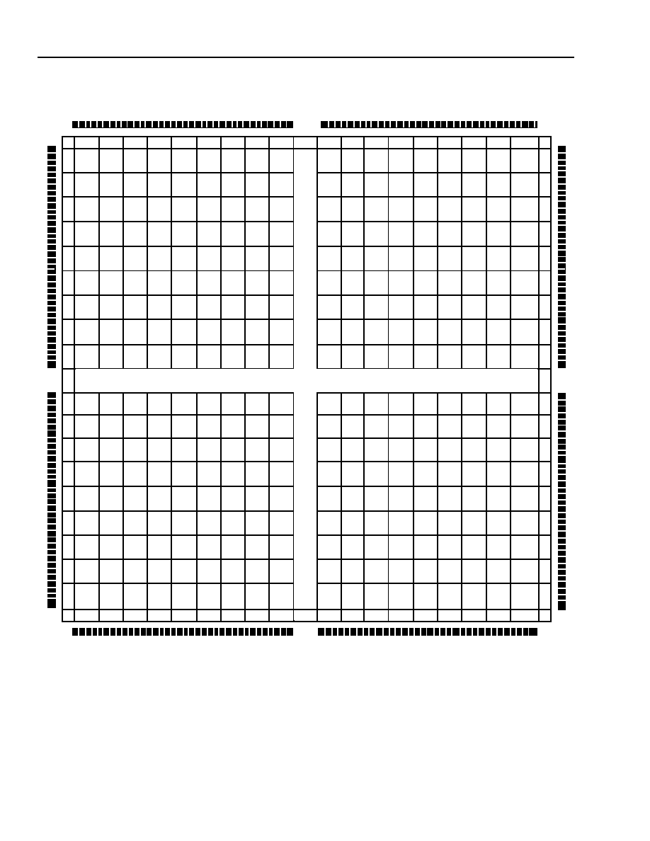
ments: PLCs, PICs, and system-level functions. Figure
1 shows an array of programmable logic cells (PLCs)
surrounded by programmable input/output cells (PICs).
Also shown are the interquad routing blocks (hIQ, vIQ)
present in Series 3. System-level functions (located in
the corners of the array) and the routing resources and
configuration RAM are not shown in Figure 1.
The OR3C/T55 array in Figure 1 has PLCs arranged in
an array of 18 rows and 18 columns. The location of a
PLC is indicated by its row and column so that a PLC in
the second row and the third column is R2C3. PICs are
located on all four sides of the FPGA between the
PLCs and the device edge. PICs are indicated using
PT and PB to designate PICs on the top and bottom
sides of the array, respectively, and PL and PR to des-
ignate PICs along the left and right sides of the array,
respectively. The position of a PIC on an edge of the
array is indicated by a number, counting from left to
right for PT and PB and top to bottom for PL and PR
PICs.
Each PIC contains routing resources and four program-
mable I/Os (PIOs). Each PIO contains the necessary
I/O buffers to interface to bond pads. PIOs in Series 3
FPGAs also contain input and output FFs, fast open-
drain capability on output buffers, special output logic
functions, and signal multiplexing/demultiplexing capa-
bilities.
PLCs comprise a programmable function unit (PFU), a
supplemental logic and interconnect cell (SLIC), and
routing resources. The PFU is the main logic element
of the PLC, containing elements for both combinatorial
and sequential logic. Combinatorial logic is done in
look-up tables (LUTs) located in the PFU. The PFU can
be used in different modes to meet different logic
requirements. The LUT's twin-quad architecture pro-
vides a configurable medium-/large-grain architecture
that can be used to implement from one to eight inde-
pendent combinatorial logic functions or a large num-
ber of complex logic functions using multiple LUTs. The
flexibility of the LUT to handle wide input functions, as
well as multiple smaller input functions, maximizes the
gate count per PFU while increasing system speed.
The LUTs can be programmed to operate in one of
three modes: combinatorial, ripple, or memory. In com-
binatorial mode, the LUTs can realize any 4- or 5-input
logic function and many multilevel logic functions using
ORCA
's softwired LUT (SWL) connections. In ripple
mode, the high-speed carry logic is used for arithmetic
functions, comparator functions, or enhanced data path
functions. In memory mode, the LUTs can be used as a
32 x 4 synchronous read/write or read-only memory, in
either single- or dual-port mode.
10
Lucent Technologies Inc.
Data Sheet
June 1999
ORCA Series 3C and 3T FPGAs
Architecture
(continued)
5-4489(F)
Figure 1. OR3C/T55 Array
VI
P
L
9
P
L
8
P
L
7
P
L
6
PL
5
P
L
4
PL
3
P
L
2
PL
1
P
L13
P
L12
P
L11
PR
1
2
PR
1
1
PR
9
PR
8
PR
7
PR
6
PR
5
PR
4
PR
3
PR
2
PR
1
PR
1
3
P
R
1
8
PR
1
7
PR
1
6
PR
1
5
PR
1
4
RM
I
D
PR
1
0
PT1
PT2
PT3
PT4
PT5
PT6
PT7
PT8
PT9
PT11
PT12
R1C1
R1C2
R1C3
R1C4
R1C5
R1C6
R1C7
R1C8
R1C9
R1C10
R1C18
R1C17
R1C16
R1C15
R1C14
R1C13
R1C12
R1C11
PT13
PT14
PT15
PT16
PT17
PT18
PB1
PB2
PB3
PB4
PB5
PB6
PB7
PB8
PB9
PB10
PB11
PB12
PL
1
8
PL
1
7
PL
1
6
PL
1
5
PL
1
4
PB13
PB14
PB15
PB16
PB17
PB18
P
L10
BMID
PT10
vIQ
R2C1
R2C2
R2C3
R2C4
R2C5
R2C6
R2C7
R2C8
R2C9
R2C10
R3C1
R3C2
R3C3
R3C4
R3C5
R3C6
R3C7
R3C8
R3C9
R3C10
R4C1
R4C2
R4C3
R4C4
R4C5
R4C6
R4C7
R4C8
R4C9
R4C10
R5C1
R5C2
R5C3
R5C4
R5C5
R5C6
R5C7
R5C8
R5C9
R5C10
R6C1
R6C2
R6C3
R6C4
R6C5
R6C6
R6C7
R6C8
R6C9
R6C10
R7C1
R7C2
R7C3
R7C4
R7C5
R7C6
R7C7
R7C8
R7C9
R7C10
R8C1
R8C2
R8C3
R8C4
R8C5
R8C6
R8C7
R8C8
R8C9
R8C10
R9C1
R9C2
R9C3
R9C4
R9C5
R9C6
R9C7
R9C8
R9C9
R9C10
R10C1 R10C2 R10C3
R10C4 R10C5 R10C6
R10C7 R10C8 R10C9
R10C10
R2C18
R2C17
R2C16
R2C15
R2C14
R2C13
R2C12
R2C11
R3C18
R3C17
R13C16
R3C15
R3C14
R3C13
R3C12
R3C11
R4C18
R4C17
R4C16
R4C15
R4C14
R4C13
R4C12
R4C11
R5C18
R5C17
R5C16
R5C15
R5C14
R5C13
R5C12
R5C11
R6C18
R6C17
R6C16
R6C15
R6C14
R6C13
R6C12
R6C11
R7C18
R7C17
R7C16
R7C15
R7C14
R7C13
R7C12
R7C11
R8C18
R8C17
R8C16
R8C15
R8C14
R8C13
R8C12
R8C11
R9C18
R9C17
R9C16
R9C15
R9C14
R9C13
R9C12
R9C11
R10C18
R10C17
R10C16
R10C15
R10C14
R10C13
R10C12
R10C11
R18C18
R18C17
R18C16
R18C15
R18C14
R18C13
R18C12
R18C11
R17C18
R17C17
R17C16
R17C15
R17C14
R17C13
R17C12
R17C11
R16C18
R16C17
R16C16
R16C15
R16C14
R16C13
R16C12
R16C11
R15C18
R15C17
R15C16
R15C15
R15C14
R15C13
R15C12
R15C11
R14C18
R14C17
R14C16
R14C15
R14C14
R14C13
R14C12
R14C11
R13C18
R13C17
R13C16
R13C15
R13C14
R13C13
R13C12
R13C11
R12C18
R12C17
R12C16
R12C15
R12C14
R12C13
R12C12
R12C11
R11C18
R11C17
R11C16
R11C15
R11C14
R11C13
R11C12
R11C11
R18C10
R18C9
R18C8
R18C7
R18C6
R18C5
R18C4
R18C3
R18C2
R18C1
R17C10
R17C9
R17C8
R17C7
R17C6
R17C5
R17C4
R17C3
R17C2
R17C1
R16C10
R16C9
R16C8
R16C7
R16C6
R16C5
R16C4
R16C3
R16C2
R16C1
R15C10
R15C9
R15C8
R15C7
R15C6
R15C5
R15C4
R15C3
R15C2
R15C1
R14C10
R14C9
R14C8
R14C7
R14C6
R14C5
R14C4
R14C3
R14C2
R14C1
R13C10
R13C9
R13C8
R13C7
R13C6
R13C5
R13C4
R13C3
R13C2
R13C1
R12C10
R12C9
R12C8
R12C7
R12C6
R12C5
R12C4
R12C3
R12C2
R12C1
R11C10
R11C9
R11C8
R11C7
R11C6
R11C5
R11C4
R11C3
R11C2
R11C1
hIQ
TMID
LM
I
D
Lucent Technologies Inc.
11
Data Sheet
June 1999
ORCA Series 3C and 3T FPGAs
Programmable Logic Cells
The programmable logic cell (PLC) consists of a pro-
grammable function unit (PFU), a supplemental logic
and interconnect cell (SLIC), and routing resources. All
PLCs in the array are functionally identical with only
minor differences in routing connectivity for improved
routability. The PFU, which contains eight 4-input LUTs,
eight latches/FFs, and one FF for logic implementation,
is discussed in the next section, followed by discus-
sions of the SLIC and PLC routing resources.
Programmable Function Unit
The PFUs are used for logic. Each PFU has 50 external
inputs and 18 outputs and can operate in several
modes. The functionality of the inputs and outputs
depends on the operating mode.
The PFU uses 36 data input lines for the LUTs, eight
data input lines for the latches/FFs, five control inputs
(ASWE, CLK, CE, LSR, SEL), and a carry input (CIN)
for fast arithmetic functions and general-purpose data
input for the ninth FF. There are eight combinatorial data
outputs (one from each LUT), eight latched/registered
outputs (one from each latch/FF), a carry-out (COUT),
and a registered carry-out (REGCOUT) that comes from
the ninth FF. The carry-out signals are used principally
for fast arithmetic functions.
Figure 2 and Figure 3 show high-level and detailed
views of the ports in the PFU, respectively. The eight
sets of LUT inputs are labeled as K
0
through K
7
with
each of the four inputs to each LUT having a suffix of
_x, where x is a number from 0 to 3. There are four F5
inputs labeled A through D. These inputs are used for a
fifth LUT input for 5-input LUTs or as a selector for multi-
plexing two 4-input LUTs. The eight direct data inputs to
the latches/FFs are labeled as DIN[7:0]. Registered LUT
outputs are shown as Q
[7:0], and combinatorial LUT
outputs are labeled as F
[7:0].
The PFU implements combinatorial logic in the LUTs
and sequential logic in the latches/FFs. The LUTs are
static random access memory (SRAM) and can be used
for read/write or read-only memory.
Each latch/FF can accept data from its associated LUT.
Alternatively, the latches/FFs can accept direct data
from DIN[7:0], eliminating the LUT delay if no combina-
torial function is needed. Additionally, the CIN input can
be used as a direct data source for the ninth FF. The
LUT outputs can bypass the latches/FFs, which reduces
the delay out of the PFU. It is possible to use the LUTs
and latches/FFs more or less independently, allowing,
for instance, a comparator function in the LUTs simulta-
neously with a shift register in the FFs.
5-5752(F)
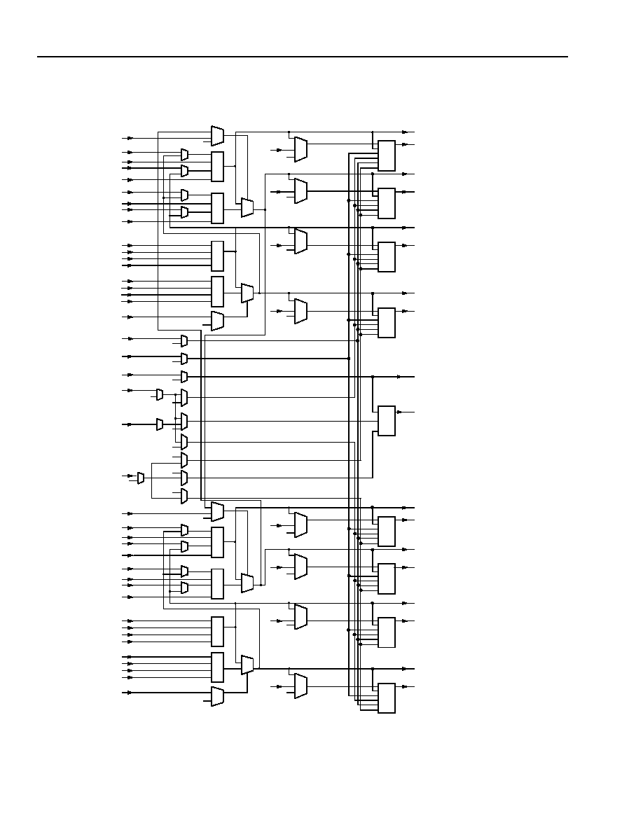
Figure 2. PFU Ports
The PFU can be configured to operate in four modes:
logic mode, half-logic mode, ripple mode, and memory
(RAM/ROM) mode. In addition, ripple mode has four
submodes and RAM mode can be used in either a
single- or dual-port memory fashion. These submodes
of operation are discussed in the following sections.
5-5752(F)
F5D
K
7
_0
K
7
_1
K
7
_2
K
7
_3
K
6
_0
K
6
_1
K
6
_2
K
6
_3
K
5
_0
K
5
_1
K
5
_2
K
5
_3
K
4
_0
K
4
_1
K
4
_2
K
4
_3
F5C
DIN7
DIN6
DIN5
DIN4
DIN3
DIN2
DIN1
DIN0
CIN
F5B
K
3
_0
K
3
_1
K
3
_2
K
3
_3
K
2
_0
K
2
_1
K
2
_2
K
2
_3
K
1
_0
K
1
_1
K
1
_2
K
1
_3
K
0
_0
K
0
_1
K
0
_2
K
0
_3
F5A
LSR
CLK
CE
SEL
ASWE
PROGRAMMABLE
FUNCTION UNIT
(PFU)
Q7
Q6
Q5
Q4
Q3
Q2
Q1
Q0
COUT
REGCOUT
F7
F6
F5
F4
F3
F2
F1
F0
12
Lucent Technologies Inc.
Data Sheet
June 1999
ORCA Series 3C and 3T FPGAs
Programmable Logic Cells
(continued)
5-5743(F)
Note: All multiplexers without select inputs are configuration selector multiplexers.
Figure 3. Simplified PFU Diagram
SEL
CIN
D
CE
CK
S/R
FF8
REGCOUT
COUT
1
ASWE
LSR
K7_3
K6_0
K6_1
K6_2
K6_3
K5_0
K5_1
K5_2
F5D
K7_0
K7_1
K7_2
K5_3
K4_0
K4_1
K4_2
K4_3
F5C
CLK
A
B
C
D
A
B
C
D
A
B
C
D
K4
K5
K6
K7
DIN7
DIN6
DIN5
DIN4
REG5
D0
D1
CE
CK
S/R
DSEL
Q5
F5
REG6
D0
D1
CE
CK
S/R
DSEL
Q6
F6
REG7
D0
D1
CE
CK
S/R
DSEL
Q7
F7
REG4
D0
D1
CE
CK
S/R
DSEL
Q4
F4
A
B
C
D
F5MODE45
K3_3
K2_0
K2_1
K2_2
K2_3
K1_0
K1_1
K1_2
F5B
K3_0
K3_1
K3_2
K1_3
K0_0
K0_1
K0_2
K0_3
F5A
A
B
C
D
A
B
C
D
A
B
C
D
K0
K1
K2
K3
DIN3
DIN2
DIN1
DIN0
REG1
D0
D1
CE
CK
S/R
DSEL
Q1
F1
REG2
D0
D1
CE
CK
S/R
DSEL
Q2
F2
REG3
D0
D1
CE
CK
S/R
DSEL
Q3
F3
REG0
D0
D1
CE
CK
S/R
DSEL
Q0
F0
A
B
C
D
F5MODE01
F5MODE67
F5MODE23
0
0
0
0
0
0
0
0
0
0
0
0
CE
0
0
0
1
1
1
0
0
0
0
1
0
1
0
1
0
1
0

Lucent Technologies Inc.
13
Data Sheet
June 1999
ORCA Series 3C and 3T FPGAs
Programmable Logic Cells
(continued)
Look-Up Table Operating Modes
The operating mode affects the functionality of the PFU input and output ports and internal PFU routing. For exam-
ple, in some operating modes, the DIN[7:0] inputs are direct data inputs to the PFU latches/FFs. In memory mode,
the same DIN[7:0] inputs are used as a 4-bit write data input bus and a 4-bit write address input bus into LUT
memory.
Table 3 lists the basic operating modes of the LUT. Figure 4--Figure 10 show block diagrams of the LUT operating
modes. The accompanying descriptions demonstrate each mode's use for generating logic.
PFU Control Inputs
Each PFU has five routable control inputs and an active-low, asynchronous global set/reset (GSRN) signal that
affects all latches and FFs in the device. The five control inputs are CLK, LSR, CE, ASWE, and SEL, and their
functionality for each logic mode of the PFU (discussed subsequently) is shown in Table 4. The clock signal to the
PFU is CLK, CE stands for clock enable, which is its primary function. LSR is the local set/reset signal that can be
configured as synchronous or asynchronous. The selection of set or reset is made for each latch/FF and is not a
function of the signal itself. ASWE stands for add/subtract/write enable, which are its functions, along with being an
optional clock enable, and SEL is used to dynamically select between direct PFU input and LUT output data as the
input to the latches/FFs.
All of the control signals can be disabled and/or inverted via the configuration logic. A disabled clock enable indi-
cates that the clock is always enabled. A disabled LSR indicates that the latch/FF never sets/resets (except from
GSRN). A disabled SEL input indicates that DIN[7:0] PFU inputs are routed to the latches/FFs. For logic and ripple
modes of the PFU, the LSR, CE, and ASWE (as a clock enable) inputs can be disabled individually for each nibble
(latch/FF[3:0], latch/FF[7:4]) and for the ninth FF.
Table 3. Look-Up Table Operating Modes
Mode
Function
Logic
4- and 5-input LUTs; softwired LUTs; latches/FFs with direct input or LUT input; CIN as direct input to
ninth FF or as pass through to COUT.
Half Logic/
Half Ripple
Upper four LUTs and latches/FFs in logic mode; lower four LUTs and latches/FFs in ripple mode; CIN
and ninth FF for logic or ripple functions.
Ripple
All LUTs combined to perform ripple-through data functions. Eight LUT registers available for direct-in
use or to register ripple output. Ninth FF dedicated to ripple out, if used. The submodes of ripple mode
are adder/subtractor, counter, multiplier, and comparator.
Memory
All LUTs and latches/FFs used to create a 32 x 4 synchronous dual-port RAM. Can be used as single-
port or as ROM.
14
Lucent Technologies Inc.
Data Sheet
June 1999
ORCA Series 3C and 3T FPGAs
Programmable Logic Cells
(continued)
Table 4. Control Input Functionality
Mode
CLK
LSR
CE
ASWE
SEL
Logic
CLK to all latches/
FFs
LSR to all latches/
FFs, enabled per nib-
ble and for ninth FF
CE to all latches/FFs,
selectable per nibble
and for ninth FF
CE to all latches/FFs,
selectable per nibble
and for ninth FF
Select between LUT
input and direct input
for eight latches/FFs
Half Logic/
Half Ripple
CLK to all latches/
FFs
LSR to all latches/FF,
enabled per nibble
and for ninth FF
CE to all latches/FFs,
selectable per nibble
and for ninth FF
Ripple logic control
input
Select between LUT
input and direct input
for eight latches/FFs
Ripple
CLK to all latches/
FFs
LSR to all latches/
FFs, enabled per nib-
ble and for ninth FF
CE to all latches/FFs,
selectable per nibble
and for ninth FF
Ripple logic control
input
Select between LUT
input and direct input
for eight latches/FFs
Memory
(RAM)
CLK to RAM
Port enable 2
Port enable 1
Write enable
Not used
Memory
(ROM)
Optional for sync.
outputs
Not used
Not used
Not used
Not used
Logic Mode
The PFU diagram of Figure 3 represents the logic
mode of operation. In logic mode, the eight LUTs are
used individually or in flexible groups to implement user
logic functions. The latches/FFs may be used in con-
junction with the LUTs or separately with the direct
PFU data inputs. There are three basic submodes of
LUT operation in PFU logic mode: F4 mode, F5 mode,
and softwired LUT (SWL) mode. Combinations of these
submodes are possible in each PFU.
F4 mode, shown simplified in Figure 4, illustrates the
uses of the basic 4-input LUTs in the PFU. The output
of an F4 LUT can be passed out of the PFU, captured
at the LUTs associated latch/FF, or multiplexed with the
adjacent F4 LUT output using one of the F5[A:D] inputs
to the PFU. Only adjacent LUT pairs (K
0
and K
1
, K
2
and K
3
, K
4
and K
5
, K
6
and K
7
) can be multiplexed, and
the output always goes to the even-numbered output of
the pair.
The F5 submode of the LUT operation, shown simpli-
fied in Figure 4, indicates the use of 5-input LUTs to
implement logic. 5-input LUTs are created from two
4-input LUTs and a multiplexer. The F5 LUT is the
same as the multiplexing of two F4 LUTs described
previously with the constraint that the inputs to the F4
LUTs be the same. The F5[A:D] input is then used as
the fifth LUT input. The equations for the two F4 LUTs
will differ by the assumed value for the F5[A:D] input,
one F4 LUT assuming that the F5[A:D] input is zero,
and the other assuming it is a one. The selection of the
appropriate F4 LUT output in the F5 MUX by the
F5[A:D] signal creates a 5-input LUT. Any combination
of F4 and F5 LUTs is allowed per PFU using the eight
16-bit LUTs. Examples are eight F4 LUTs, four F5
LUTs, and a combination of four F4 plus two F5 LUTs.
5-5970(F)
Figure 4. Simplified F4 and F5 Logic Modes
K
7
F7
K
7
F6
K
6
F5D
K
6
F6
K
5
F5
K
5
F4
K
4
F5C
K
4
F4
K
3
F3
K
3
F2
K
2
F5B
K
2
F2
K
1
F1
K
1
F0
K
0
F5A
K
0
F0
K
7
/K
6
F6
K
5
/K
4
F4
K
3
/K
2
F2
K
1
/K
0
F0
F5 MODE
MULTIPLEXED F4 MODE
F4 MODE
Lucent Technologies Inc.
15
Data Sheet
June 1999
ORCA Series 3C and 3T FPGAs
Programmable Logic Cells
(continued)
Softwired LUT submode uses F4 and F5 LUTs and internal PFU feedback routing to generate complex logic func-
tions up to three LUT-levels deep. Figure 3 shows multiplexers between the K
Z
[3:0] inputs to the PFU and the
LUTs. These multiplexers can be independently configured to route certain LUT outputs to the input of other LUTs.
In this manner, very complex logic functions, some of up to 21 inputs, can be implemented in a single PFU at
greatly enhanced speeds.
Figure 5 shows several softwired LUT topologies. In this figure, each circle represents either an F4 or F5 LUT. It is
important to note that an LUT output that is fed back for softwired use is still available to be registered or output
from the PFU. This means, for instance, that a logic equation that is needed by itself and as a term in a larger
equation need only be generated once and PLC routing resources will not be required to use it in the larger equa-
tion.
Figure 5. Softwired LUT Topology Examples
5-5753(F)
F4
KEY:
F5
4-INPUT LUT
5-INPUT LUT
5-5754(F)
F4
F4
F4
F4
F4
F4
F4
F4
FOUR 7-INPUT FUNCTIONS IN ONE PFU
F5
F5
F5
F5
TWO 9-INPUT FUNCTIONS IN ONE PFU
F5
F5
F5
F5
ONE 17-INPUT FUNCTION IN ONE PFU
F5
F5
F4
ONE 21-INPUT FUNCTION IN ONE PFU
F4
F4
F4
F4
F4
F4
F4
TWO OF FOUR 10-INPUT FUNCTIONS IN ONE PFU
F4
F4
F4
F4
3
ONE OF TWO 12-INPUT FUNCTIONS IN ONE PFU
16
16
Lucent Technologies Inc.
Data Sheet
June 1999
ORCA Series 3C and 3T FPGAs
Programmable Logic Cells
(continued)
Half-Logic Mode
Series 3 FPGAs are based upon a twin-quad architec-
ture in the PFUs. The byte-wide nature (eight LUTs,
eight latches/FFs) may just as easily be viewed as two
nibbles (two sets of four LUTs, four latches/FFs). The
two nibbles of the PFU are organized so that any nib-
ble-wide feature (excluding some softwired LUT topolo-
gies) can be swapped with any other nibble-wide
feature in another PFU. This provides for very flexible
use of logic and for extremely flexible routing. The half-
logic mode of the PFU takes advantage of the twin-
quad architecture and allows half of a PFU, K
[7:4]
and
associated latches/FFs, to be used in logic mode while
the other half of the PFU, K
[3:0]
and associated latches/
FFs, is used in ripple mode. In half-logic mode, the
ninth FF may be used as a general-purpose FF or as a
register in the ripple mode carry chain.
Ripple Mode
The PFU LUTs can be combined to do byte-wide ripple
functions with high-speed carry logic. Each LUT has a
dedicated carry-out net to route the carry to/from any
adjacent LUT. Using the internal carry circuits, fast
arithmetic, counter, and comparison functions can be
implemented in one PFU. Similarly, each PFU has
carry-in (CIN, FCIN) and carry-out (COUT, FCOUT)
ports for fast-carry routing between adjacent PFUs.
The ripple mode is generally used in operations on two
data buses. A single PFU can support an 8-bit ripple
function. Data buses of 4 bits and less can use the
nibble-wide ripple chain that is available in half-logic
mode. This nibble-wide ripple chain is also useful for
longer ripple chains where the length modulo 8 is four
or less. For example, a 12-bit adder (12 modulo 8 = 4)
can be implemented in one PFU in ripple mode (8 bits)
and one PFU in half-logic mode (4 bits), freeing half of
a PFU for general logic mode functions.
Each LUT has two operands and a ripple (generally
carry) input, and provides a result and ripple (generally
carry) output. A single bit is rippled from the previous
LUT and is used as input into the current LUT. For LUT
K
0
, the ripple input is from the PFU CIN or FCIN port.
The CIN/FCIN data can come from either the fast-carry
routing (FCIN) or the PFU input (CIN), or it can be tied
to logic 1 or logic 0.
In the following discussions, the notations LUT K
7
/K
3
and F[7:0]/F[3:0]
are used to denote the LUT that pro-
vides the carry-out and the data outputs for full PFU
ripple operation (K
7
, F[7:0]) and half-logic ripple
operation (K
3
, F[3:0]), respectively. The ripple mode
diagram in Figure 6 shows full PFU ripple operation,
with half-logic ripple connections shown as dashed
lines.
The result output and ripple output are calculated by
using generate/propagate circuitry. In ripple mode, the
two operands are input into K
Z
[1] and K
Z
[0] of each
LUT. The result bits, one per LUT, are F[7:0]/F[3:0]
(see
Figure 6). The ripple output from LUT K
7
/K
3
can be
routed on dedicated carry circuitry into any of four adja-
cent PLCs, and it can be placed on the PFU COUT/
FCOUT outputs. This allows the PLCs to be cascaded
in the ripple mode so that nibble-wide ripple functions
can be expanded easily to any length.
Result outputs and the carry-out may optionally be reg-
istered within the PFU. The capability to register the
ripple results, including the carry output, provides for
improved counter performance and simplified pipelin-
ing in arithmetic functions.
Figure 6. Ripple Mode
5-5755(F)
F7
K
7
[1]
K
7
[0]
K
7
D
Q
C
C
D Q
Q7
REGCOUT
COUT
F6
K
6
[1]
K
6
[0]
K
6
D
Q
Q6
F4
K
4
[1]
K
4
[0]
K
4
D
Q
Q4
F3
K
3
[1]
K
3
[0]
K
3
D
Q
Q3
F2
K
2
[1]
K
2
[0]
K
2
D
Q
Q2
F1
K
1
[1]
K
1
[0]
K
1
D
Q
Q1
F5
K
5
[1]
K
5
[0]
K
5
D
Q
Q5
F0
K
0
[1]
K
0
[0]
K
0
D
Q
Q0
CIN/FCIN
FCOUT
Lucent Technologies Inc.
17
Data Sheet
June 1999
ORCA Series 3C and 3T FPGAs
Programmable Logic Cells
(continued)
The ripple mode can be used in one of four submodes.
The first of these is adder-subtractor submode. In
this submode, each LUT generates three separate out-
puts. One of the three outputs selects whether the
carry-in is to be propagated to the carry-out of the cur-
rent LUT or if the carry-out needs to be generated. If
the carry-out needs to be generated, this is provided by
the second LUT output. The result of this selection is
placed on the carry-out signal, which is connected to
the next LUT carry-in or the COUT/FCOUT signal, if it
is the last LUT (K
7
/K
3
). Both of these outputs can be
any equation created from K
Z
[1] and K
Z
[0], but in this
case, they have been set to the propagate and gener-
ate functions.
The third LUT output creates the result bit for each LUT
output connected to F[7:0]/F[3:0]. If an adder/subtrac-
tor is needed, the control signal to select addition or
subtraction is input on ASWE, with a logic 0 indicating
subtraction and a logic 1 indicating addition. The result
bit is created in one-half of the LUT from a single bit
from each input bus K
Z
[1:0], along with the ripple input
bit.
The second submode is the counter submode (see
Figure 7). The present count, which may be initialized
via the PFU DIN inputs to the latches/FFs, is supplied
to input K
Z
[0], and then output F[7:0]/F[3:0] will either
be incremented by one for an up counter or decre-
mented by one for a down counter. If an up/down
counter is needed, the control signal to select the direc-
tion (up or down) is input on ASWE with a logic 1 indi-
cating an up counter and a logic 0 indicating a down
counter. Generally, the latches/FFs in the same PFU
are used to hold the present count value.
Figure 7. Counter Submode
5-5756(F)
F7
K
7
[0]
K
7
D
Q
C
C
D
Q
Q7
REGCOUT
COUT
F6
K
6
[0]
K
6
D
Q
Q6
F4
K
4
[0]
K
4
D
Q
Q4
F3
K
3
[0]
K
3
D
Q
Q3
F2
K
2
[0]
K
2
D
Q
Q2
F1
K
1
[0]
K
1
D
Q
Q1
F5
K
5
[0]
K
5
D
Q
Q5
F0
K
0
[0]
K
0
D
Q
Q0
CIN/FCIN
FCOUT
18
18
Lucent Technologies Inc.
Data Sheet
June 1999
ORCA Series 3C and 3T FPGAs
Programmable Logic Cells
(continued)
In the third submode, multiplier submode, a single
PFU can affect an 8 x 1 bit (4 x 1 for half-ripple mode)
multiply and sum with a partial product (see Figure 8).
The multiplier bit is input at ASWE, and the multiplicand
bits are input at K
Z
[1], where K
7
[1] is the most signifi-
cant bit (MSB). K
Z
[0] contains the partial product (or
other input to be summed) from a previous stage. If
ASWE is logical 1, the multiplicand is added to the par-
tial product. If ASWE is logical 0, 0 is added to the par-
tial product, which is the same as passing the partial
product. CIN/FCIN can bring the carry-in from the less
significant PFUs if the multiplicand is wider than 8 bits,
and COUT/FCOUT holds any carry-out from the multi-
plication, which may then be used as part of the prod-
uct or routed to another PFU in multiplier mode for
multiplicand width expansion.
Ripple mode's fourth submode features equality
comparators. The functions that are explicitly available
are A
>
B, A
B, and A
<
B, where the value for A is
input on K
Z
[0], and the value for B is input on K
Z
[1]. A
value of 1 on the carry-out signals valid argument. For
example, a carry-out equal to 1 in AB submode indi-
cates that the value on K
Z
[0] is greater than or equal to
the value on K
Z
[1]. Conversely, the functions A < B, A +
B, and A > B are available using the same functions but
with a 0 output expected. For example, A
>
B with a 0
output indicates A < B. Table 5 shows each function
and the output expected.
If larger than 8 bits, the carry-out signal can be cas-
caded using fast-carry logic to the carry-in of any adja-
cent PFU. The use of this submode could be shown
using Figure 6, except that the CIN/FCIN input for the
least significant PFU is controlled via configuration.
Key: C = configuration data.
Figure 8. Multiplier Submode
Table 5. Ripple Mode Equality Comparator
Functions and Outputs
Equality
Function
ORCA
Foundry
Submode
True, if
Carry-Out Is:
A
>
B
A
>
B
1
A
<
B
A
<
B
1
A
B
A
B
1
A < B
A
>
B
0
A > B
A
<
B
0
A = B
A
B
0
5-5757(F)
K
7
[1]
K
7
[0]
+
D Q
C
C
D Q
1
0
0
K
7
ASWE
K
4
[1]
K
4
[0]
+
D Q
1
0
0
K
4
K
3
[1]
K
3
[0]
+
D Q
1
0
0
K
3
K
2
[1]
K
2
[0]
+
D Q
1
0
0
K
2
K
1
[1]
K
1
[0]
+
D Q
1
0
0
K
1
K
6
[1]
K
6
[0]
+
D Q
1
0
0
K
6
K
5
[1]
K
5
[0]
+
D Q
1
0
0
K
5
K
0
[1]
K
0
[0]
+
D Q
1
0
0
K
0
F7
Q7
REGCOUT
COUT
F6
Q6
F4
Q4
F3
Q3
F2
Q2
F1
Q1
F5
Q5
F0
Q0
Lucent Technologies Inc.
19
Data Sheet
June 1999
ORCA Series 3C and 3T FPGAs
Programmable Logic Cells
(continued)
Memory Mode
The Series 3 PFU can be used to implement a 32 x 4 (128-bit) synchronous, dual-port random access memory
(RAM). A block diagram of a PFU in memory mode is shown in Figure 9. This RAM can also be configured to work
as a single-port memory and because initial values can be loaded into the RAM during configuration, it can also be
used as a read-only memory (ROM).
Figure 9. Memory Mode
The PFU memory mode uses all LUTs and latches/FFs including the ninth FF in its implementation as shown in
Figure 9. The read address is input at the K
Z
[3:0] and F5[A:D] inputs where K
Z
[0] is the LSB and F5[A:D] is the
MSB, and the write address is input on CIN (MSB) and DIN[7, 5, 3, 1], with DIN[1] being the LSB. Write data is
input on DIN[6, 4, 2, 0], where DIN[6] is the MSB, and read data is available combinatorially on F[6, 4, 2, 0] and
registered on Q[6, 4, 2, 0] with F[6] and Q[6] being the MSB. The write enable signal is input at ASWE, and two
write port enables are input on CE and LSR. The PFU CLK signal is used to synchronously write the data. The
polarities of the clock, write enable, and port enables are all programmable. Write-port enables may be disabled if
they are not to be used.
5-5969(F)
Q6
Q4
Q2
Q0
D
5
Q
CIN(WA4)
K
Z
[3:0]
4
F5[A:D]
D Q
DIN7(WA3)
D Q
DIN5(WA2)
D Q
DIN3(WA1)
D Q
DIN1(WA0)
D Q
DIN6(WD3)
D Q
DIN4(WD2)
D Q
DIN2(WD1)
D Q
DIN0(WD0)
D Q
ASWE(WREN)
EN
S/R
CE(WPE1)
LSR(WPE2)
CLK
4
WRITE
WRITE
READ
READ
4
F6
F4
F2
F0
D Q
D Q
D Q
D Q
WRITE
RAM CLOCK
ADDRESS[4:0]
ADDRESS[4:0]
DATA[3:0]
DATA[3:0]
ENABLE
20
20
Lucent Technologies Inc.
Data Sheet
June 1999
ORCA Series 3C and 3T FPGAs
Programmable Logic Cells
(continued)
Data is written to the write data, write address, and
write enable registers on the active edge of the clock,
but data is not written into the RAM until the next clock
edge one-half cycle later. The read port is actually
asynchronous, providing the user with read data very
quickly after setting the read address, but timing is also
provided so that the read port may be treated as fully
synchronous for write then read applications. If the
read and write address lines are tied together (main-
taining MSB to MSB, etc.), then the dual-port RAM
operates as a synchronous single-port RAM. If the
write enable is disabled, and an initial memory contents
is provided at configuration time, the memory acts as a
ROM (the write data and write address ports and write
port enables are not used).
Wider memories can be created by operating two or
more memory mode PFUs in parallel, all with the same
address and control signals, but each with a different
nibble of data. To increase memory word depth above
32, two or more PLCs can be used. Figure 10 shows a
128 x 8 dual-port RAM that is implemented in eight
PLCs. This figure demonstrates data path width expan-
sion by placing two memories in parallel to achieve an
8-bit data path. Depth expansion is applied to achieve
128 words deep using the 32-word deep PFU memo-
ries. In addition to the PFU in each PLC, the SLIC
(described in the next section) in each PLC is used for
read address decodes and 3-state drivers. The 128 x 8
RAM shown could be made to operate as a single-port
RAM by tying (bit-for-bit) the read and write addresses.
To achieve depth expansion, one or two of the write
address bits (generally the MSBs) are routed to the
write port enables as in Figure 10. For 2 bits, the bits
select which 32-word bank of RAM of the four available
from a decode of two WPE inputs is to be written. Simi-
larly, 2 bits of the read address are decoded in the
SLIC and are used to control the 3-state buffers
through which the read data passes. The write data
bus is common, with separate nibbles for width expan-
sion, across all PLCs, and the read data bus is com-
mon (again, with separate nibbles) to all PLCs at the
output of the 3-state buffers.
Figure 10 also shows a new optional capability to pro-
vide a read enable for RAMs/ROMs in Series 3 using
the SLIC cell. The read enable will 3-state the read
data bus when inactive, allowing the write data and
read data buses to be tied together if desired.
Figure 10. Memory Mode Expansion Example--128 x 8 RAM
5-5749(F)
RD[7:0]
WE
WA[6:0]
RA[6:0]
CLK
WA
RA
WPE0
WPE1
WE
WD[7:4]
5
5
4
PLC
8
WD[7:0]
8
7
7
WA
RA
WPE0
WPE1
WE
RD[3:0]
WD[3:0]
5
5
4
PLC
RD[7:4]
WA
RA
WPE0
WPE1
WE
WD[7:4]
5
5
4
PLC
WA
RA
WPE0
WPE1
WE
RD[3:0]
WD[3:0]
5
5
4
PLC
RD[7:4]
RE
4
4
4
4
PFU
PFU
PFU
PFU
SLIC
SLIC
SLIC
SLIC

Lucent Technologies Inc.
21
Data Sheet
June 1999
ORCA Series 3C and 3T FPGAs
Programmable Logic Cells
(continued)
Supplemental Logic and Interconnect Cell
(SLIC)
Each PLC contains a supplemental logic and intercon-
nect cell (SLIC) embedded within the PLC routing, out-
side of the PFU. As its name indicates, the SLIC
performs both logic and interconnect (routing) func-
tions. Its main features are 3-statable, bidirectional buff-
ers, and a
PAL
-like decoder capability. Figure 11 shows
a diagram of a SLIC with all of its features shown. All
modes of the SLIC are not available at one time.
Each SLIC contains ten bidirectional (BIDI) buffers,
each buffer capable of driving left and/or right out of the
SLIC. These BIDI buffers are twin-quad in nature and
are segregated into two groups of four (nibbles) and a
third group of two for control. Each of these groups of
BIDIs can drive from the left (BLI[9:0]) to the right
(BRO[9:0]), the right (BRI[9:0]) to the left (BLO[9:0]), or
from the central input (I[9:0]) to the left and/or right.
This central input comes directly from the PFU outputs
(O[9:0]). Each of the BIDIs in the nibble-wide groups
also has a 3-state buffer capability, but not the third
group.
There is one 3-state control (TRI) for each SLIC, with
the capability to invert or disable the 3-state control for
each group of four BIDIs. Separate 3-state control for
each nibble-wide group is achievable by using the
SLIC's decoder (DEC) output, driven by the group of
two BIDIs, to control the 3-state of one BIDI nibble
while using the TRI signal to control the 3-state of the
other BIDI nibble. Figure 12 and Figure 13 show the
SLIC in buffer mode with available 3-state control from
the TRI and DEC signals. If the entire SLIC is acting in
a buffer capacity, the DEC output may be used to gen-
erate a constant logic 1 (VHI) or logic 0 (VLO) signal for
general use.
The SLIC may also be used to generate
PAL
-like AND-
OR with optional INVERT (AOI) functions or a decoder
of up to 10 bits. Each group of buffers can feed into an
AND gate (4-input AND for the nibble groups and 2-
input AND for the other two buffers). These AND gates
then feed into a 3-input gate that can be configured as
either an AND gate or an OR gate. The output of the 3-
input gate is invertible and is output at the DEC output
of the SLIC. Figure 16 shows the SLIC in full decoder
mode.
The functionality of the SLIC is parsed by the two
nibble-wide groups and the 2-bit buffer group. Each of
these groups may operate independently as BIDI buff-
ers (with or without 3-state capability for the nibble-
wide groups) or as a
PAL
/decoder.
As discussed in the memory mode section, if the SLIC
is placed into one of the modes where it contains both
buffers and a decode or AOI function (e.g.,
BUF_BUF_DEC mode), the DEC output can be gated
with the 3-state input signal. This allows up to a 6-input
decode (e.g., BUF_DEC_DEC mode) plus the 3-state
input to control the enable/disable of up to four buffers
per SLIC. Figure 12--Figure 16 show several configu-
rations of the SLIC, while Table 6 shows all of the possi-
ble modes.
Table 6. SLIC Modes
Mode
#
Mode
BUF
[3:0]
BUF
[7:4]
BUF
[9:8]
1
BUFFER
Buffer
Buffer
Buffer
2
BUF_BUF_DEC
Buffer
Buffer
Decoder
3
BUF_DEC_BUF
Buffer
Decoder
Buffer
4
BUF_DEC_DEC
Buffer
Decoder Decoder
5
DEC_BUF_BUF
Decoder
Buffer
Buffer
6
DEC_BUF_DEC Decoder
Buffer
Decoder
7
DEC_DEC_BUF
Decoder Decoder
Buffer
8
DECODER
Decoder Decoder Decoder
22
22
Lucent Technologies Inc.
Data Sheet
June 1999
ORCA Series 3C and 3T FPGAs
Programmable Logic Cells
(continued)
Figure 11. SLIC All Modes Diagram
Figure 12. Buffer Mode
5-5744(F)
BRI9
I9
BLI9
BRI8
I8
BLI8
BRI7
I7
BLI7
BRI6
I6
BLI6
BRI5
I5
BLI5
BRI4
I4
BLI4
BRI3
I3
BLI3
BRI2
I2
BLI2
BRI1
I1
BLI1
BRI0
I0
BLI0
BL09
BR09
BL08
BR08
BL07
BR07
BL06
BR06
BL05
BR05
BL04
BR04
BL03
BR03
BL02
BR02
BL01
BR01
BL00
BR00
DEC
DEC
0/1
0/1
TRI
0/1
0/1
HIGH Z WHEN LOW
5-5745(F)
BRI9
I9
BLI9
BRI8
I8
BLI8
BRI7
I7
BLI7
BRI6
I6
BLI6
BRI5
I5
BLI5
BRI4
I4
BLI4
BRI3
I3
BLI3
BRI2
I2
BLI2
BRI1
I1
BLI1
BRI0
I0
BLI0
BL09
BR09
BL08
BR08
BL07
BR07
BL06
BR06
BL05
BR05
BL04
BR04
BL03
BR03
BL02
BR02
BL01
BR01
BL00
BR00
TRI
0/1
0/1
1
0
DEC
THIS CAN BE USED
A VHI OR VLO
HIGH Z WHEN LOW
TO GENERATE
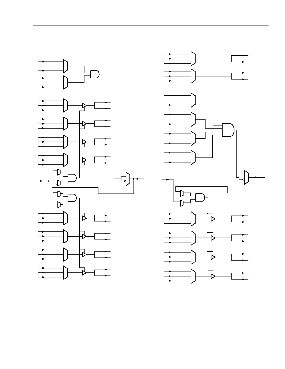
Lucent Technologies Inc.
23
Data Sheet
June 1999
ORCA Series 3C and 3T FPGAs
Programmable Logic Cells
(continued)
Figure 13. Buffer-Buffer-Decoder Mode
Figure 14. Buffer-Decoder-Buffer Mode
5-5746(F)
BRI9
BLI9
BRI8
BLI8
BRI7
I7
BLI7
BRI6
I6
BLI6
BRI5
I5
BLI5
BRI4
I4
BLI4
BRI3
I3
BLI3
BRI2
I2
BLI2
BRI1
I1
BLI1
BRI0
I0
BLI0
BL07
BR07
BL06
BR06
BL05
BR05
BL04
BR04
BL03
BR03
BL02
BR02
BL01
BR01
BL00
BR00
TRI
DEC
1
1
1
1
HIGH Z
WHEN LOW
HIGH Z
WHEN LOW
5-5747(F)
BRI7
BLI7
BRI6
BLI6
BRI5
BLI5
BRI4
BLI4
BRI3
I3
BLI3
BRI2
I2
BLI2
BRI1
I1
BLI1
BRI0
I0
BLI0
BL03
BR03
BL02
BR02
BL01
BR01
BL00
BR00
TRI
DEC
BRI9
I9
BLI9
BRI8
I8
BLI8
BL09
BR09
BL08
BR08
1
1
HIGH Z WHEN LOW
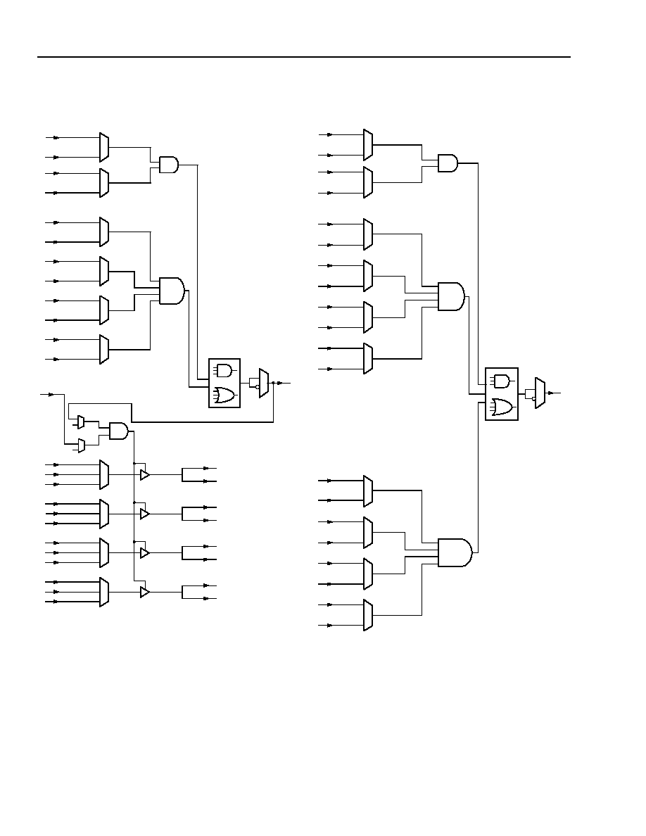
24
24
Lucent Technologies Inc.
Data Sheet
June 1999
ORCA Series 3C and 3T FPGAs
Programmable Logic Cells
(continued)
Figure 15. Buffer-Decoder-Decoder Mode
Figure 16. Decoder Mode
5-5750(F)
BRI7
BLI7
BRI6
BLI6
BRI5
BLI5
BRI4
BLI4
BRI3
I3
BLI3
BRI2
I2
BLI2
BRI1
I1
BLI1
BRI0
I0
BLI0
BL03
BR03
BL02
BR02
BL01
BR01
BL00
BR00
TRI
DEC
BRI9
BLI9
BRI8
BLI8
1
1
HIGH Z WHEN LOW
5-5748(F)
BRI7
BLI7
BRI6
BLI6
BRI5
BLI5
BRI4
BLI4
BRI3
BLI3
BRI2
BLI2
BRI1
BLI1
BRI0
BLI0
DEC
BRI9
BLI9
BRI8
BLI8

Lucent Technologies Inc.
25
Data Sheet
June 1999
ORCA Series 3C and 3T FPGAs
Programmable Logic Cells
(continued)
PLC Latches/Flip-Flops
The eight general-purpose latches/FFs in the PFU can
be used in a variety of configurations. In some cases,
the configuration options apply to all eight latches/FFs in
the PFU and
some apply to the latches/FFs on a nibble-
wide basis where the ninth FF is considered indepen-
dently. For other options, each latch/FF is independently
programmable. In addition, the ninth FF can be used for
a variety of functions.
Table 7 summarizes these latch/FF options. The
latches/FFs can be configured as either positive- or
negative-level sensitive latches, or positive or negative
edge-triggered flip-flops (the ninth register can only be
FF). All latches/FFs in a given PFU share the same
clock, and the clock to these latches/FFs can be
inverted. The input into each latch/FF is from either the
corresponding LUT output (F[7:0]) or the direct data
input (DIN[7:0]). The latch/FF input can also be tied to
logic 1 or to logic 0, which is the default.
* Not available for FF[8].
The eight latches/FFs in a PFU share the clock (CLK)
and options for clock enable (CE), local set/reset (LSR),
and front-end data select (SEL) inputs. When CE is dis-
abled, each latch/FF retains its previous value when
clocked. The clock enable, LSR, and SEL inputs can be
inverted to be active-low.
The set/reset operation of the latch/FF is controlled by
two parameters: reset mode and set/reset value. When
the global set/reset (
GSRN) and local set/reset (LSR)
signals are not asserted, the latch/FF operates normally.
The reset mode is used to select a synchronous or
asynchronous LSR operation. If synchronous, LSR has
the option to be enabled only if clock enable (CE or
ASWE) is active or for LSR to have priority over the
clock enable input, thereby setting/resetting the FF inde-
pendent of the state of the clock enable. The clock
enable is supported on FFs, not latches. It is imple-
mented by using a 2-input multiplexer on the FF input,
with one input being the previous state of the FF and the
other input being the new data applied to the FF. The
select of this 2-input multiplexer is clock enable (CE or
ASWE), which selects either the new data or the previ-
ous state. When the clock enable is inactive, the FF out-
put does not change when the clock edge arrives.
Table 7. Configuration RAM Controlled Latch/
Flip-Flop Operation
Function Options
Common to All Latches/FFs in PFU
LSR Operation
Asynchronous or synchronous
Clock Polarity
Noninverted or inverted
Front-end Select*
Direct (DIN[7:0]) or from LUT (F[7:0])
LSR Priority
Either LSR or CE has priority
Latch/FF Mode
Latch or flip-flop
Enable GSRN
GSRN enabled or has no effect on
PFU latches/FFs
Set Individually in Each Latch/FF in PFU
Set/Reset Mode
Set or reset
By Group (Latch/FF[3:0], Latch/FF[7:4], and FF[8])
Clock Enable
CE or ASWE or none
LSR Control
LSR or none
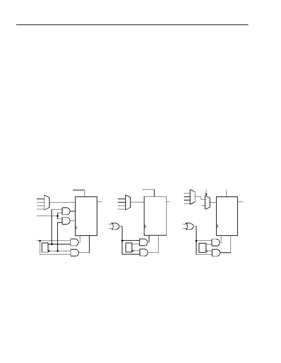
26
26
Lucent Technologies Inc.
Data Sheet
June 1999
ORCA Series 3C and 3T FPGAs
Programmable Logic Cells
(continued)
The GSRN signal is only asynchronous, and it sets/
resets all latches/FFs in the FPGA based upon the set/
reset configuration bit for each latch/FF. The set/reset
value determines whether GSRN and LSR are set or
reset inputs. The set/reset value is independent for
each latch/FF. A new option is available to disable the
GSRN function per PFU after initial device configura-
tion.
The latch/FF can be configured to have a data front-
end select. Two data inputs are possible in the front-
end select mode, with the SEL signal used to select
which data input is used. The data input into each
latch/FF is from the output of its associated LUT, F[7:0],
or direct from DIN[7:0], bypassing the LUT. In the front-
end data select mode, both signals are available to the
latches/FFs.
If either or both of these inputs is unused or is unavail-
able, the latch/FF data input can be tied to a logic 0 or
logic 1 instead (the default is logic 0).
The latches/FFs can be configured in three basic
modes:
1. Local synchronous set/reset: the input into the
PFU's LSR port is used to synchronously set or
reset each latch/FF.
2. Local asynchronous set/reset: the input into LSR
asynchronously sets or resets each latch/FF.
3. Latch/FF with front-end select, LSR either synchro-
nous or asynchronous: the data select signal
selects the input into the latches/FFs between the
LUT output and direct data in.
For all three modes, each latch/FF can be indepen-
dently programmed as either set or reset. Figure 17
provides the logic functionality of the front-end select,
global set/reset, and local set/reset operations.
The ninth PFU FF, which is generally associated with
registering the carry-out signal in ripple mode func-
tions, can be used as a general-purpose FF. It is only
an FF and is not capable of being configured as a latch.
Because the ninth FF is not associated with an LUT,
there is no front-end data select. The data input to the
ninth FF is limited to the CIN input, logic 1, logic 0, or
the carry-out in ripple and half-logic modes.
Key: C = configuration data.
Figure 17. Latch/FF Set/Reset Configurations
DIN
LOGIC 0
LOGIC 1
F
CE
D
s_set
s_reset
CLK
SET RESET
Q
LSR
GSRN
CD
CE/ASWE
D
CLK
SET RESET
LSR
CD
CE
CE/ASWE
D
CLK
SET RESET
CD
CE
CE/ASWE
DIN
SEL
GSRN
DIN
LOGIC 0
LOGIC 1
F
DIN
LOGIC 0
LOGIC 1
F
LSR
GSRN
Q
Q
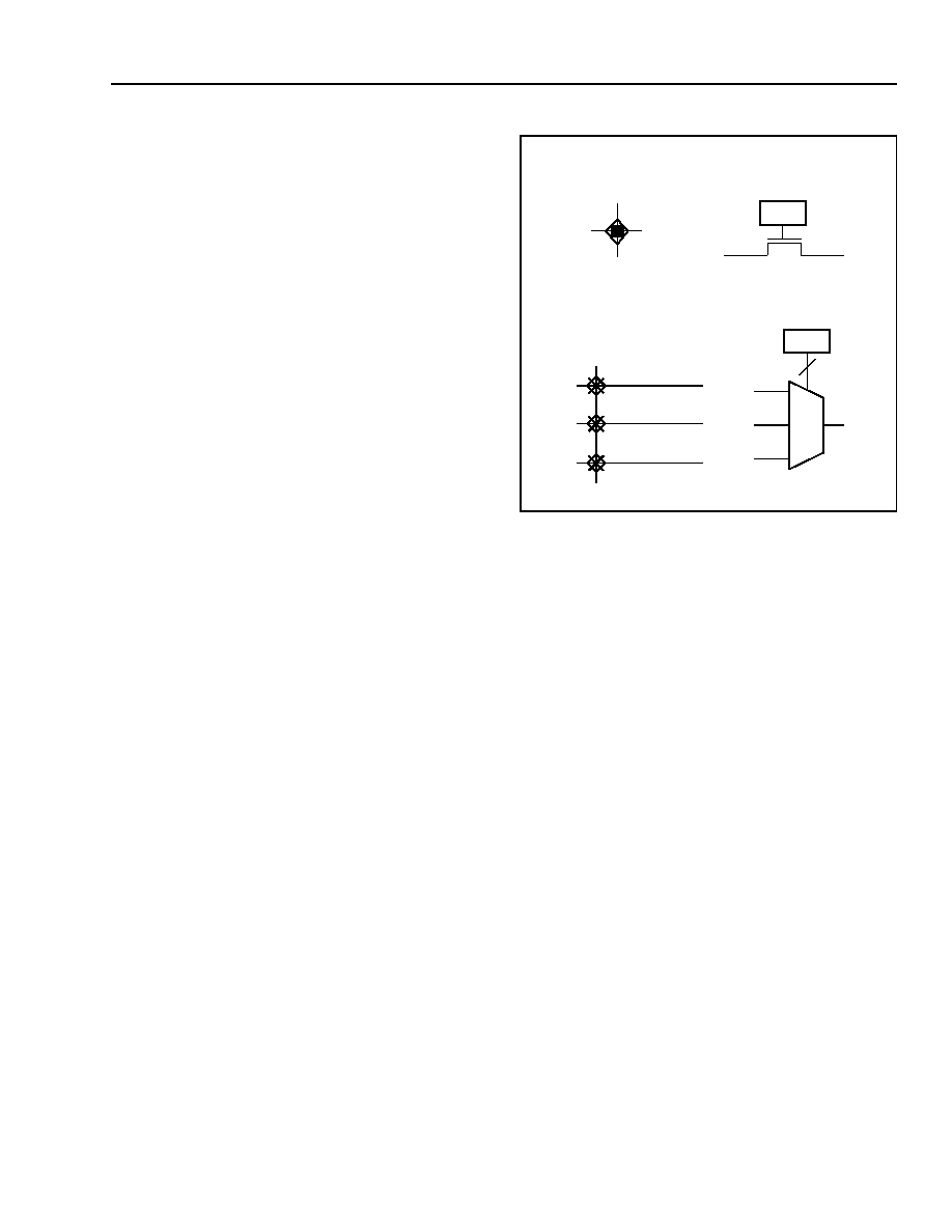
Lucent Technologies Inc.
27
Data Sheet
June 1999
ORCA Series 3C and 3T FPGAs
Programmable Logic Cells
(continued)
PLC Routing Resources
Generally, the
ORCA
Foundry
Development System is
used to automatically route interconnections. Interac-
tive routing with the
ORCA
Foundry design editor
(EPIC) is also available for design optimization. To use
EPIC for interactive layout, an understanding of the
routing resources is needed and is provided in this sec-
tion.
The routing resources consist of switching circuitry and
metal interconnect segments. Generally, the metal lines
which carry the signals are designated as routing seg-
ments. The switching circuitry connects the routing
segments, providing one or more of three basic func-
tions: signal switching, amplification, and isolation. A
net running from a PFU or PIC output (source) to a
PLC or PIC input (destination) consists of one or more
routing segments, connected by switching circuitry
called configurable interconnect points (CIPs).
The following sections discuss PLC, PIC, and interquad
routing resources. This section discusses the PLC
switching circuitry, intra-PLC routing, inter-PLC routing,
and clock distribution.
Configurable Interconnect Points
The process of connecting routing segments uses
three basic types of switching circuits: two types of con-
figurable interconnect points (CIPs) and bidirectional
buffers (BIDIs). The basic element in CIPs is one or
more pass transistors, each controlled by a configura-
tion RAM bit. The two types of CIPs are the mutually
exclusive (or multiplexed) CIP and the independent CIP.
A mutually exclusive set of CIPs contains two or more
CIPs, only one of which can be on at a time. An inde-
pendent CIP has no such restrictions and can be on
independent of the state of other CIPs. Figure 18
shows an example of both types of CIPs.
Key: C = configuration data.
5-5973(C)
Figure 18. Configurable Interconnect Point
3-Statable Bidirectional Buffers
Bidirectional buffers, previously described in the SLIC
section of the programmable logic cell discussion, pro-
vide isolation as well as amplification for signals routed
a long distance. Bidirectional buffers are also used to
route signals diagonally in the PLC (described later in
the subsection entitled Intra-PLC Routing), and BIDIs
can be used to indirectly route signals through the
switching routing (xSW) segments. Any number from
zero to ten BIDIs can be used in a given PLC.
MULTIPLEXED CIP
A
B
C
O
A
B
C
O
CD
INDEPENDENT CIP
A
B
CD
B
A
=
2
28
Lucent Technologies Inc.
Data Sheet
June 1999
ORCA Series 3C and 3T FPGAs
Programmable Logic Cells
(continued)
General Routing Structure
Routing resources in Series 3 FPGAs generally consist of routing segments in groups of ten, with varying lengths
and connectivity to logic and other routing resources. The varying lengths of routing segments provides a hierarchy
of routing capability from chip-length routes to routes within a PLC. The hierarchical nature of the routing provides
the
ORCA
Foundry development tools with the necessary resources to route a design completely and to optimize
the routing for system speed while reducing the overall power required by the device.
Within each group of ten routing segments there is an equivalency of connectivity between pairs of segments.
These pairs are segments: [0, 4] and [1, 5] and [2, 6] and [3, 7] and [8, 9]. The equivalency in connectivity ensures
that signals on either segment in a pair have the same capability to get to a given destination. This, in turn, allows
for signal distribution from a source to varying destinations without using special routing. It also provides for routing
flexibility by ensuring that one segment position will not become so congested as to preclude routing a bus or group
of signals and allows easy connectivity from either of the twin quads in a source PFU to either of the twin quads in
any destination PFU.
Having ten segments in a group is significant in that it provides for routing a byte of data and two control signals or
parity. Due to the equivalent pairs of segments, this can also be viewed as routing two nibbles each with a control
signal. Figure 19 is an overview of the routing for a single PLC.
5-5766(F)
Figure 19. Single PLC View of Inter-PLC Route Segments
2 OF 5
LINE-BY-LINE
FINS
PFU
OUTPUT
SLIC
SWITCHING
SUR[9:0]
BL[
9:
0]
vxL
[9
:0
]
vx5
[9
:0
]
v
x
1L[
9:
0]
SU
L[
9
:
0]
vx1
R[9
:0
]
FC
LC
K
VC
K
vxH
[9
:0
]
BL[
9:
0]
hxH[9:0]
hx1U[9:0]
hCK
FC
SLL[9:0]
hx1B[9:0]
hx5[9:0]
hxL[9:0]
BR[9:0]
SUL[9:0]
BL[9:0]
FC
SUL[9:0]
BR[9:0]
LCK
SLL[9:0]
FC
SLR[9:0]
5
2
5
2
5
2
KEY: CONFIGURABLE SIGNAL LINE BREAKS

Lucent Technologies Inc.
29
Data Sheet
June 1999
ORCA Series 3C and 3T FPGAs
Programmable Logic Cells
(continued)
Intra-PLC Routing
The function of the intra-PLC routing resources is to
connect the PFU's input and output ports to the routing
resources used for entry to and exit from the PLC. This
routing provides PFU feedback, corner turning, or
switching from one type of routing resource to another.
Flexible Input Structure (FINS)
The flexible input switching structure (FINS) in each
PLC of the
ORCA
Series 3 provides for the flexibility of
a crossbar switch from the routing resources to the
PFU inputs while taking advantage of the routability of
shared inputs. Connectivity between the PLC routing
resources and the PFU inputs is provided in two
stages. The primary FINS switch has 50 inputs that
connect the PLC routing to the 35 inputs on the sec-
ondary switch. The outputs of the second switch con-
nect to the 50 PFU inputs. The switches are
implemented to provide connectivity for bused signals
and individual connections.
PFU Output Switching
The PFU outputs are switched onto PLC routing
resources via the PFU output multiplexer (OMUX). The
PFU output switching segments from the output multi-
plexer provide ten connections to the PLC routing out
of 18 possible PFU outputs (F[7:0], Q[7:0], DOUT,
REGCOUT). These output switching segments con-
nect segment for segment to the SUR, SUL, SLR, and
SLL switching segments described below (e.g., O4
connects only to SUR4, not SUR5). The output switch-
ing segments also feed directly into the SLIC on a seg-
ment-by-segment basis. This connectivity is also
described below.
Switching Routing Segments (xSW)
There are four sets of switching routing segments in
each PLC. Each set consists of ten switching elements:
SUL[9:0], SUR[9:0], SLL[9:0], and SLR[9:0], tradition-
ally labeled for the upper-left, upper-right, lower-left,
and lower-right sections of the PFUs, respectively. The
xSW routing segments connect to the PFU inputs and
outputs as well as the BIDI routing segments, to be
described later. They also connect to both the horizon-
tal and vertical x1 and x5 routing segments (inter-PLC
routing resources, described later) in their specific cor-
ner. xSW segments can be used for fast connections
between adjacent PLCs or PICs without requiring the
use of inter-PLC routing resources. This capability not
only increases signal speed on adjacent PLC routing,
but also reduces routing congestion on the principal
inter-PLC routing resources. The SLL and SUR seg-
ments combine to provide connectivity to the PLCs to
the left and right of the current PLC; the SLR and SUL
segments combine to provide connectivity to the PLCs
above and below the current PLC.
Fast routes on switching segments to diagonally adja-
cent PLCs/PICs are possible using the BIDI routing
segments (discussed below) and the SLL and SLR
switching segments. The BR BIDI routing segments
combine with the SUL switching segments of the PLC
below and to the right of the current PLC to connect to
that PLC. The BL BIDI routing segments combine with
the SLL switching segments of the PLC above and to
the right of the current PLC to connect to that PLC.
These fast diagonal connections provide a great
amount of flexibility in routing congested areas of logic
and in shifting data on a per-PLC basis such as per-
forming implicit multiplications/divisions in routing
between functional logic elements.
Switching routing segments are also the chief means
by which signals are transferred between the inter-PLC
routing resources and the PFU. Each set of switching
segments has connectivity to the x1 routing segments,
and there is varying connectivity to the x5, xH, and xL
inter-PLC routing segments. Detailed information on
switching segment/inter-PLC routing connectivity is
provided later in this section in the Inter-PLC Routing
Resources subsection.

30
30
Lucent Technologies Inc.
Data Sheet
June 1999
ORCA Series 3C and 3T FPGAs
Programmable Logic Cells
(continued)
BIDI Routing and SLIC Connectivity
The SLIC is connected to the rest of the PLC by the
bidirectional (BIDI) routing segments and the PFU out-
put switching segments coming from the PFU output
multiplexer. The BIDI routing segments (xBID) are
labeled as BL for BIDI-left and BR for BIDI-right. Each
set of BR and BL xBID segments is composed of ten
bidirectional lines (note that these lines are diagramed
as ten input lines to the SLIC and ten output lines from
the SLIC that can be used in a mutually exclusive fash-
ion). Because the SLIC is connected directly to the out-
puts of the PFU, it provides great flexibility in routing via
the xBID segments. The PFU routing segments, O[9:0],
only connect to their respective line in the SLL, SUL,
SUR, and SLR switching segment groups. That is, O9
only connects to SLL9, SUL9, SUR9, and SLR9. The
BIDI lines provide the capability to connect to the other
member of the routing set. That means, for example,
that O9 can be routed to BR8 or BL8. This connectivity
can be used as a means to distribute or gather signals
on intra-PLC routing without disturbing inter-PLC
resources. As described in the Switching Routing Seg-
ments subsection, the BIDI routing segments are also
used for routes to a diagonally adjacent PFU.
In addition to the intra-PLC connections, the xBID and
output switching segments also have connectivity to
the x1, x5, and xL inter-PLC routing resources, provid-
ing an alternate routing path rather than using PLC
xSW segments. These connections also provide a path
to the 3-state buffers in the SLIC without encumbering
the xSW segments. In this manner, buffering or 3-state
control can be added to inter-PLC routing without dis-
turbing local functionality within a PFU.
Control Signal and Fast-Carry Routing
PFU control signal and the fast-carry routing are per-
formed using the FINS structure and several dedicated
routing paths. The fast-carry (FC) routing resources
consist of a dedicated bidirectional segment between
each orthogonal pair of PLCs. This means that a fast-
carry can go to or come from each PLC to the right or
left, above or below the subject PLC. The FINS struc-
ture is used to control the switching of these fast-carry
paths between the fast-carry input (FCIN) and fast-
carry output (FCOUT) ports of the PFU.
The PFU control inputs (CE, SEL, LSR, ASWE) and
CIN can be reached via the FINS by two special routing
segments, E1 and E2. The E1 routing segment pro-
vides connectivity between all of the xBID routing seg-
ments and the FINS. It is unidirectional from the BIDI
routing to the FINS. E1 also provides connectivity to the
PFU clock input via FINS for a local clock signal. The
E2 segment connects the SLIC DEC output to the FINS
and to a group of CIPS that provide bidirectional con-
nectivity with all of the BIDI routing segments. This
allows the DEC signal to be used in the PFU and/or
routed on the BIDI segments. It also allows signals to
be routed to the PFU on the xBID segments if the SLIC
DEC output is not used.
There is also a dedicated routing segment from the
FINS
to the SLIC TRI input used for BIDI buffer 3-state
control.
Lucent Technologies Inc.
31
Data Sheet
June 1999
ORCA Series 3C and 3T FPGAs
Programmable Logic Cells
(continued)
Inter-PLC Routing Resources
The inter-PLC routing is used to route signals between
PLCs. The routing segments occur in groups of ten,
and differ in the numbers of PLCs spanned. The x1
routing segments span one PLC, the x5 routing seg-
ments span five PLCs, the xH routing segments span
one-half the width (height) of the PLC array, and the xL
routing segments span the width (height) of the PLC
array. All types of routing segments run in both horizon-
tal and vertical directions.
Table 8 shows the groups of inter-PLC routing seg-
ments in each PLC. In the table, there are two rows/col-
umns for x1 lines. They are differentiated by a T for top,
B for bottom, L for left, and R for right. In the
ORCA
Foundry design editor representation, the horizontal x1
routing segments are located above and below the
PFU. The two groups of vertical segments are located
on the left side of the PFU. The xL and x5 routing seg-
ments only run below and to the left of the PFU, while
the xH segments only run above and to the right of the
PFU. The indexes specify individual routing segments
within a group. For example, the vx5[2] segment runs
vertically to the left of the PFU, spans five PLCs, and is
the third line in the 10-bit wide group.
PLCs are arranged like tiles on the
ORCA
device.
Breaks in routing occur at the middle of the tile (e.g., x1
lines break in the middle of each PLC) and run across
tiles until the next break.
Figure 20 provides a global view of inter-PLC routing
resources across multiple PLCs.
x1 Routing Segments. There are a total of 40 x1 rout-
ing segments per PLC: 20 vertical and 20 horizontal.
Each of these are subdivided into two, 10-bit wide
buses: hx1T[9:0], hx1B[9:0], vx1L[9:0], and vx1R[9:0].
An x1 segment is one PLC long. If a signal net is longer
than one PLC, an x1 segment can be lengthened to n
times its length by turning on n ≠ 1 CIPs. A signal is
routed onto an x1 route segment via the switching rout-
ing segments or BIDI routing segments which also
allows the x1 route segment to be connected to other
inter-PLC segments of different lengths. Corner turning
between x1 segments is provided through direct con-
nections, xSW segments, and xBID segments.
x5 Routing Segments. There are two sets of ten x5
routing segments per PLC. One set (vx5[9:0]) runs ver-
tically, and the other (hx5[9:0]) runs horizontally. Each
x5 segment traverses five PLCs before it is broken by a
CIP. Two x5 segments in each group break in each
PLC. The two that break are in an equivalent pair; for
example, x5[0] and x5[4]. The x5 segments that break
shift by one at the next PLC. For example, if hx5[0] and
hx5[4] are broken at the current PLC, hx5[1] and hx5[5]
will be broken at the PLC to the right of the current
PLC. There are direct connections to the BIDI routing
segments in the PLC at which the x5 segments break,
on both sides of the break. Signal corner turning is
enabled by CIPs in each PLC that allow the broken x5
segments to directly connect to the broken x5 seg-
ments that run in the orthogonal direction. x5 corner
turning can also be accomplished via the xSW and
xBID segments in a PLC. In addition, the x5 segments
are connected to the FINS and PFU outputs on a bit-
by-bit basis by the xSW segments. x5 segments can be
connected for signal runs in multiples of five PLCs, or
they can be combined with x1 and xH routing segments
for runs of varying distances.
Table 8. Inter-PLC Routing Resources
Horizontal
Routing
Segments
Vertical
Routing
Segments
Distance
Spanned
hx1U[9:0]
vx1R[9:0]
One PLC
hx1B[9:0]
vx1L[9:0]
One PLC
hx5[9:0]
vx5[9:0]
Five PLCs
hx5[9:0]
vx5[9:0]
Five PLCs
hxL[9:0]
vxL[9:0]
PLC Array
hxH[9:0]
vxH[9:0]
1/2 PLC Array
hCLK
vCLK
PLC Array
32
Lucent Technologies Inc.
Data Sheet
June 1999
ORCA Series 3C and 3T FPGAs
Programmable Logic Cells
(continued)
5-5767(F)
Figure 20. Multiple PLC View of Inter-PLC Routing
PFU
PFU
PFU
PFU
PFU
PFU
PFU
PFU
PFU
hxH[9:0]
hx1[9:0]
hCLK
hx1[9:0]
hx5[9:0]
hxL[9:0]
hxH[9:0]
hx1[9:0]
hCLK
hx1[9:0]
hx5[9:0]
hxL[9:0]
hx1[9:0]
hx5[9:0]
hxL[9:0]
hxH[9:0]
hx1[9:0]
hCLK
vx1L[
9:0]
vx5[9
:0]
vCLK
vxH[9:0
]
vx1[9
:0]
vxL[9
:0]
vx5[9
:0]
vCLK
vxH[9:0
]
vxL[9
:0]
vx5[9
:0]
vx1[9
:0]
vCLK
vxH[9:0
]
vx1[9
:0]
vx1[9
:0]
vx1[9
:0]
vx1[9:0
]
10
2
2
10
2
10
2
10
2
10
2
10
2
10
2
10
2
10
2
10
10
2
10
2
10
2
10
2
10
2
10
2
10
2
10
2
SLIC
SLIC
SLIC
SLIC
SLIC
SLIC
SLIC
SLIC
SLIC
PLC BOUNDARY
2 OF 10
LINE-BY-LINE
10
2
KEY: CONFIGURABLE SIGNAL-LINE BREAKS:

Lucent Technologies Inc.
33
Data Sheet
June 1999
ORCA Series 3C and 3T FPGAs
Programmable Logic Cells
(continued)
xL Routing Lines. The xL routing lines run vertically
and horizontally the height and width of the array,
respectively. There are a total of 20 xL routing lines per
PLC: ten horizontal (hxL[9:0]) and ten vertical
(vxL[9:0]). Each of the xL lines connects to the PIC
routing at either end. The xL lines are intended prima-
rily for global signals that must travel long distances
and require minimum delay and/or skew, such as
clocks or 3-state buses.
Each xL line (also called a long line) drives a buffer in
each PLC that can drive onto the horizontal and verti-
cal local clock routing segments (lCLK) in the PLC.
Also, two out of each group of ten xL segments in each
PLC can be driven by a buffer attached to a clock spine
(described later) allowing local distribution of global
clock signals. More general-purpose connections to the
long lines can be made through the xBID segments in a
PLC. Each long line is connected to an xBID segment
on a bit-by-bit basis. These BIDI connections allow cor-
ner turning from horizontal to vertical long lines, and
connection between long lines and x1 or x5 segments.
xH Routing Segments. Ten by-half (xH) routing seg-
ments run horizontally (hxH[9:0]) and ten xH routing
segments run vertically (vxH[9:0]) in each row and col-
umn in the array. These routing segments travel a dis-
tance of one-half the PLC array before being broken in
the middle of the array in the interquad area (discussed
later). They also connect at the periphery of the FPGA
to the PICs, like the xL lines. xH routing segments con-
nect to the PLCs only by switching segments. They are
intended for fast signal interconnect.
Clock (and Global CE and LSR) Routing Segments.
For a very fast and low-skew clock (or other global sig-
nal tree), clock routing segments run the entire height
and width of the PLC array. There are two clock routing
segments per PLC: one horizontal (hCLK) and one ver-
tical (vCLK). The source for these clock routing seg-
ments can be any of the I/O buffers in the PIC, the
Series 3 ExpressCLK inputs, user logic, or the pro-
grammable clock manager (PCM). The horizontal clock
routing segments (hCLK) are alternately driven by the
left and right PICs. The vertical clock routing segments
(vCLK) are alternately driven by the top and bottom
PICs.
The clock routing segments are designed to be a clock
spine. In each PLC, there is a fast connection available
from the clock segment to a long-line driver (described
earlier). With this connection, one of the clock routing
segments in each PLC can be used to drive one of the
ten xL routing segments perpendicular to it, which, in
turn, creates a clock spine tree. This feature is dis-
cussed in detail in the Clock Distribution Network sec-
tion.
Special connectivity is provided in each PLC to connect
the clock enable signals (CE and ASWE) and the LSR
signal to the clock network for fast global control signal
distribution. CE and ASWE have a special connection
to the horizontal clock spine, and LSR has a special
connection to the vertical clock spine. This allows both
signals to be routed globally within the same PLC, if
desired; however, this will consume some of the
resources available for clock signal routing.
If using these spines, the clock enable signal must
come from the right or left edge of the device, and the
LSR signal must come from the top or bottom of the
device due to their horizontal and vertical connectivity,
respectively, to the clock network.
Minimizing Routing Delay
The CIP is an active element used to connect two rout-
ing segments. As an active element, it adds signifi-
cantly to the resistance and capacitance of a routing
network (net), thus increasing the net's delay. The
advantage of the x1 segment over an x5 segment is
routing flexibility. A net from one PLC to the next is eas-
ily routed by using x1 routing segments. As more CIPs
are added to a net, the delay increases. To increase
speed, routes that are greater than two PLCs away are
routed on the x5 routing segments because a CIP is
located only in every fifth PLC. A net that spans eight
PLCs requires seven x1 routing segments and six
CIPs. Using x5 routing segments, the same net uses
two routing segments and one CIP.

34
34
Lucent Technologies Inc.
Data Sheet
June 1999
ORCA Series 3C and 3T FPGAs
Programmable Logic Cells
(continued)
PLC Architectural Description
Figure 21 is an architectural drawing of the PLC (as
seen in
ORCA
Foundry) that reflects the PFU, the rout-
ing segments, and the CIPs. A discussion of each of
the letters in the drawing follows.
A. These are switching routing segments (xSW) that
give the router flexibility. In general switching theory,
the more levels of indirection there are in the routing,
the more routable the network is. The xSW seg-
ments can also connect to the xSW lines in adjacent
PLCs.
B. These CIPs connect the x1 routing. These are
located in the middle of the PLC to allow the block to
connect to either the left end of the horizontal x1
segment from the right or the right end of the hori-
zontal x1 segment from the left, or both. By symme-
try, the same principle is used in the vertical
direction.
C. This set of CIPs is used to connect the x1 and x5
nets to the xSW segments or to other x1 and x5
nets. The CIPs on the major diagonal allow data to
be transmitted on a bit-by-bit basis from x1 nets to
the xSW segments and between the x1 and x5 nets.
D. This structure is the supplemental logic and inter-
connect cell, or SLIC. It contains 3-statable bidirec-
tional buffers and logic for building decoders and
AND-OR-INVERT type structures.
E. These are the primary and secondary elements of
the flexible input structure or FINS. FINS is a switch
matrix that provides high connectivity while retaining
routing capability. FINS also includes feedback
paths for softwired LUT implementation.
F. This is the PFU output switch matrix. It is a complex
switch network which, like the FINS at the input, pro-
vides high connectivity and maintains routability.
G. This set of CIPs allows an xBID segment to transfer
a signal to/from xSW segments on each side. The
BIDIs can access the PFU through the xSW seg-
ments. These CIPs allow data to be routed through
the BIDIs for amplification or 3-state control and
continue to another PLC. They also provide an alter-
native routing resource to improve routability.
H. These CIPs are used to transfer data from/to the
xBID segments to/from the x1 and xL routing seg-
ments. These CIPs have been optimized to allow
the BIDI buffers to drive the loads usually seen
when using each type of routing segment.
I. Clock input to PFU.
J. These are the ten switched output routing segments
from the PFU. They connect to the PLC switching
segments and are input to the SLIC.
K. These lines deliver the auxiliary signals clock enable
(CE), local set/reset (LSR), front-end select (SEL),
add/subtract/write enable (ASWE), as well as the
carry signals (CIN and FCIN) to the latches/FFs.
L. This is the local clock buffer. Any of the horizontal
and vertical xL lines can drive the clock input of the
PLC latches/FFs. The clock routing segments
(vCLK and hCLK) and multiplexers/drivers are used
to connect to the xL routing segments for low-skew,
low-delay global signals.
M. These routing segments are used to route the fast-
carry signal to/from the neighboring four PLCs. The
carry-out (COUT) and registered carry-out (REG-
COUT) can also be routed out of the PFU.
N. This is the E2 control routing segment. It runs from
the SLIC DEC output to the FINS and also provides
connectivity to all xBID segments.
O. The xH routing segments run one-half the length
(width) of the array before being broken by a CIP.
P. These CIPs connect the xH segments to the xSW
segments.
Q. The xBID segments are used to connect the SLIC to
the xSW segments, x1 segments, x5 segments, and
xL lines, as well as providing for diagonal PLC to
PLC connections.
R. These CIPs provide connections from the xBID seg-
ments to the E1/E2 routing segments that feed PFU
control inputs CE, LSR, CIN, ASWE, SEL, and the
clock input. Alternatively, these CIPs connect the
BIDI lines to the decoder (DEC) output of the SLIC,
for routing the DEC signal.
S. These are clock spines (vCLK and hCLK) with the
multiplexers and drivers to connect to the xL routing
segments.
T. These CIPs connect xBID segments to switching
segments in diagonally and orthogonally adjacent
PFUs.
U. These CIPs connect xSW segments to the PFU out-
put segments.
V. These CIPS connect xSW segments in orthogonally
adjacent PFUs.
W.This is the SLIC 3-state control routing segment
from the FINS to the SLIC 3-state control.
X. This is the E1 control routing segment. It provides a
PFU input path from all xBID segments.
Y. These CIPs are used to select which xBID segments
are connected to the E1/E2 signal as described in
(R).
Lucent Technologies Inc.
35
Data Sheet
June 1999
ORCA Series 3C and 3T FPGAs
Programmable Logic Cells
(continued)
5-5758(F)
Figure 21. PLC Architecture
H
S
M
G
R
L
H
H
D
R
SLIC
OUTPUT
SWITCHING
PFU
P
R
I
M
ARY
F
I
N
S
SE
CON
DAR
Y F
I
N
S
B
W
Y
A
B
P
M
O
Q
M
O
F
P
V
K
J
U
U
U
X
A
B
H
B
G
C
H
Q
Q
T
M
S
Q
Q
L
H
T
E
E
N
Q
C
C
C
A
C
C
C
A
A
A
A
C
A
A
C
C
C
C
A
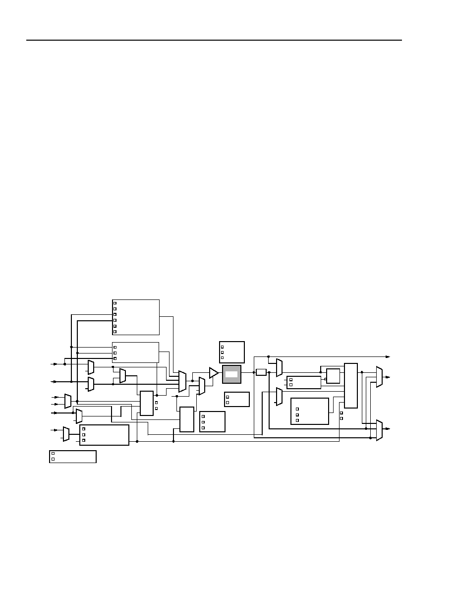
36
36
Lucent Technologies Inc.
Data Sheet
June 1999
ORCA Series 3C and 3T FPGAs
Programmable Input/Output Cells
The programmable input/output cells (PICs) are
located along the perimeter of the device. The PIC's
name is represented by a two-letter designation to indi-
cate on which side of the device it is located followed by
a number to indicate in which row or column it is
located. The first letter, P, designates that the cell is a
PIC and not a PLC. The second letter indicates the side
of the array where the PIC is located. The four sides
are left (L), right (R), top (T), and bottom (B). The indi-
vidual I/O pad is indicated by a single letter (either A, B,
C, or D) placed at the end of the PIC name. As an
example, PL10A indicates a pad located on the left
side of the array in the tenth row.
Each PIC interfaces to four bond pads and contains the
necessary routing resources to provide an interface
between I/O pads and the PLCs. Each PIC is com-
posed of four programmable I/Os (PIOs) and significant
routing resources. Each PIO contains input buffers,
output buffers, routing resources, latches/FFs, and
logic and can be configured as an input, output, or
bidirectional I/O.
PICs in the Series 3 FPGAs have significant local rout-
ing resources, similar to routing in the PLCs. This new
routing increases the ability to fix user pinouts prior to
placement and routing of a design and still maintain
routability. The flexibility provided by the routing also
provides for increased signal speed due to a greater
variety of signal paths possible.
Included in the PIC routing is a fast path from the input
pins to the SLICs in each of the three adjacent PLCs
(one orthogonal and two diagonal). This feature allows
for input signals to be very quickly processed by the
SLIC decoder function and used on-chip or sent back
off of the FPGA. Also new to the Series 3 PIOs are
latches and FFs and options for using fast, dedicated
clocks called ExpressCLKs. These features will all be
discussed in subsequent sections.
A diagram of a single PIO (one of four in a PIC) is
shown in Figure 22. Table 9 provides an overview of the
programmable functions in an I/O cell.
5-5805(F).c
Figure 22. OR3C/Txxx Programmable Input/Output (PIO) Image from
ORCA
Foundry
IN2
IN1
D0
D1
CK
SP
SD
LSR
INREGMODE
LATCHFF
LATCH
FF
D
CK
NORMAL
INVERTED
RESET
SET
LEVEL MODE
TTL
CMOS
UP
DOWN
NONE
PULL-MODE
BUFFER
TS
FAST
SLEW
SINK
RESET
SET
LSR
SP
CK
D
OUT1
OUT2
ECLK
SCLK
CE
CE_OVER_LSR
LSR_OVER_CE
ASYNC
LSR
ENABLE_GSR
DISABLE_GSR
OUT1OUTREG
OUT2OUTREG
OUT1OUT2
NOR
XOR
XNOR
AND
NAND
OR
PIO LOGIC
CLKIN
0
0
1
0
PAD
Q
Q
1
PD
TO
RO
U
TIN
G
Q
1
ECLK
SCLK
PMUX
F
R
O
M
ROU
T
IN
G
MODE
LSR
CK
D0 Q

Lucent Technologies Inc.
37
Data Sheet
June 1999
ORCA Series 3C and 3T FPGAs
Programmable Input/Output Cells
(continued)
5 V Tolerant I/O
The I/O on the OR3Txxx Series devices allow intercon-
nection to both 3.3 V and 5 V devices (selectable on a
per-pin basis).
The OR3Txxx devices will drive the pin to the 3.3 V lev-
els when the output buffer is enabled. If the other
device being driven by the OR3Txxx device has TTL-
compatible inputs, then the device will not dissipate
much input buffer power. This is because the OR3Txxx
output is being driven to a higher level than the TTL
level required. If the other device has a CMOS-compat-
ible input, the amount of input buffer power will also be
small. Both of these power values are dependent upon
the input buffer characteristics of the other device when
driven at the OR3Txxx output buffer voltage levels.
The OR3Txxx device has internal programmable pull-
ups on the I/O buffers. These pull-up voltages are
always referenced to V
DD
and are always sufficient to
pull the input buffer of the OR3Txxx device to a high
state. The pin on the OR3Txxx device will be at a level
1.0 V below V
DD
(minimum of 2.0 V with a minimum
V
DD
of 3.0 V). This voltage is sufficient to pull the exter-
nal pin up to a 3.3 V CMOS high input level (1.8 V, min)
or a TTL high input level (2.0 V, min) in a 5 V tolerant
system. Therefore, in a 5 V tolerant system using 5 V
CMOS parts, care must be taken to evaluate the use of
these pull-ups to pull the pin of the OR3Txxx device to
a typical 5 V CMOS high input level (2.2 V, min).
PCI Compliant I/O
The I/O on the OR3Txxx Series devices allows compli-
ance with PCI Local Bus (Rev. 2.2) 5 V and 3.3 V sig-
naling environments. The signaling environment used
for each input buffer can be selected on a per-pin basis.
The selection provides the appropriate I/O clamping
diodes for PCI compliance. Choosing an IBT input
buffer will provide PCI compliance in OR3Txxx devices.
OR3Cxx devices have PCI Local Bus compliant I/Os for
5 V signaling.
Table 9. PIO Options
Input
Option
Input Level
TTL, OR3Cxx only
CMOS, OR3Cxx or OR3Txxx
3.3 V PCI Compliant, OR3Txxx
5 V PCI Compliant, OR3Txxx
Input Speed
Fast, Delayed
Float Value
Pull-up, Pull-down, None
Register Mode
Latch, FF, Fast Zero Hold FF,
None (direct input)
Clock Sense
Inverted, Noninverted
Input Selection
Input 1, Input 2, Clock Input
Output
Option
Output Drive
Current
12 mA/6 mA or 6 mA/3 mA
Output Function
Normal, Fast Open Drain
Output Speed
Fast, Slewlim, Sinklim
Output Source
FF Direct-out, General Routing
Output Sense
Active-high, Active-low
3-State Sense
Active-high, Active-low (3-state)
FF Clocking
ExpressCLK
, System Clock
Clock Sense
Inverted, Noninverted
Logic Options
See Table 10.
I/O Controls
Option
Clock Enable
Active-high, Active-low,
Always Enabled
Set/Reset Level
Active-high, Active-low,
No Local Reset
Set/Reset Type
Synchronous, Asynchronous
Set/Reset Priority
CE over LSR, LSR over CE
GSR Control
Enable GSR, Disable GSR

38
38
Lucent Technologies Inc.
Data Sheet
June 1999
ORCA Series 3C and 3T FPGAs
Programmable Input/Output Cells
(continued)
Inputs
As outlined earlier in Table 9, there are six major
options on the PIO inputs that can be selected in the
ORCA
Foundry tools. For OR3Cxx devices, the inputs
and bidirectional buffers can be configured as either
TTL or CMOS compatible. OR3Txxx devices support
CMOS levels only for input or bidirectional buffers, have
5 V tolerant I/Os as previously explained, but can
optionally be selected on a pin-by-pin basis to be PCI
bus 3.3 V signaling compliant (PCI bus 5 V signaling
compliance occurs in 5 V tolerant operation). The
default buffer upon powerup for the unused sites is 5 V
tolerant/5 V PCI compliant. Consult the
ORCA
macro
library, Series 3 I/O cells, for the appropriate buffers.
Inputs may have a pull-up or pull-down resistor
selected on an input for signal stabilization and power
management. Input signals in a PIO can be passed to
PIC routing on any of three paths, two general signal
paths into PIC routing, and/or a fast route into the clock
routing system.
There is also a programmable delay available on the
input. When enabled, this delay affects the IN1 and IN2
signals of each PIO, but not the clock input. The delay
allows any signal to have a guaranteed zero hold time
when input. This feature is discussed subsequently.
Inputs should have transition times of less than 500 ns
and should not be left floating. If any pin is not used, it
is 3-stated with an internal pull-up resistor enabled
automatically after configuration.
Warning: During configuration, all OR3Txxx inputs
have internal pull-ups enabled. If these inputs are
driven to 5 V, they will draw substantial current
(
5 mA). This is due to the fact that the inputs are
pulled up to 3 V.
Floating inputs increase power consumption, produce
oscillations, and increase system noise. The OR3Cxx
inputs have a typical hysteresis of approximately 280
mV (200 mV for the OR3Txxx) to reduce sensitivity to
input noise. The PIC contains input circuitry which pro-
vides protection against latch-up and electrostatic dis-
charge.
The other features of the PIO inputs relate to the new
latch/FF structure in the input path. As shown in
Figure 23, the input is optionally passed to a register or
latch/register pair. These structures can operate in the
modes listed in Table 9. In latch mode, the input signal
is fed to a latch that is clocked by a system clock signal.
The clock may be inverted or noninverted from its
sense in the PIC routing. There is also a local set/reset
signal to the latch from the PIC routing. The senses of
these signals are also programmable as well as the
capability to enable or disable the global set/reset sig-
nal and select the set/reset priority. The same control
signals may also be used to control the input latch/FF
when it is configured as a FF instead of a latch, with the
addition of another control signal used as a clock
enable.
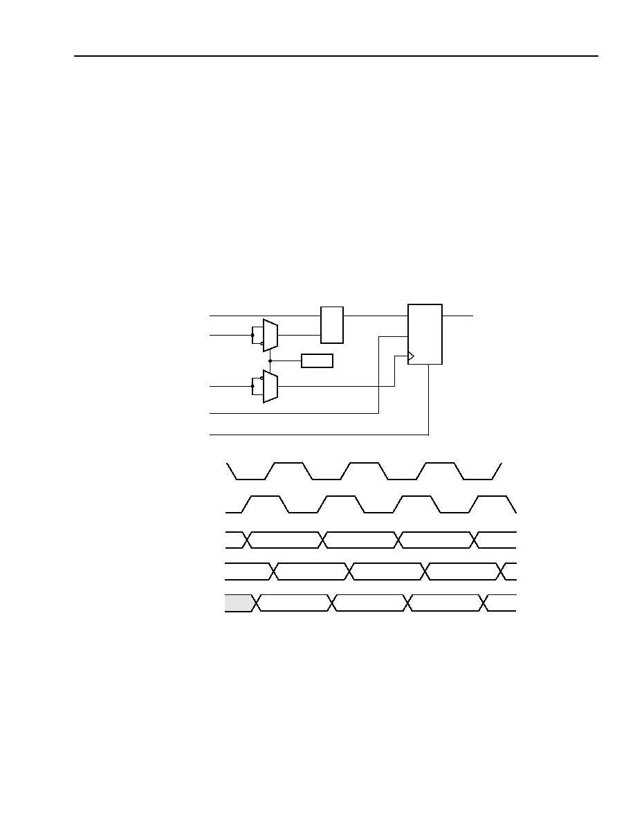
Lucent Technologies Inc.
39
Data Sheet
June 1999
ORCA Series 3C and 3T FPGAs
Programmable Input/Output Cells
(continued)
Zero-Hold Input
There are two options for zero-hold input capture in the PIO. If input delay mode is selected to delay the signal from
the input pin, data can be either registered or latched with guaranteed zero-hold time in the PIO using a system
clock.
To guarantee zero hold, the system clock spine structure must be used for clocking, as will be discussed later. The
fast zero-hold mode of the PIO input takes advantage of the latch/FF combination and sources the input FF data
from a dedicated latch that is clocked by the ExpressCLK from the PIC. The ExpressCLK is a clock from a dedi-
cated input pin designed for fast, low-skew operation at the I/Os and is described more fully in the Clock Distribu-
tion Network and PIC Interquad (MID) Routing sections that follow. The combination of ExpressCLK latch and
system clock FF guarantees a zero-hold capture of input data in the PIO FF, while at the same time reducing input
setup time. Figure 23 shows a schematic of the fast-capture latch/FF and a sample timing diagram.
5-5974(F)
Note: CE and LSR signals not shown.
Figure 23. Fast-Capture Latch and Timing
D Q
INPUT DATA
LATCH
CLK
O
I
EXPRESSCLK
O
I
SYSTEM CLK
CD = 1
CLOCK ENABLE
LOCAL SET/RESET
D
Q
FF
S/R
CE
DATA OUT
TO PIC ROUTING
EXPRESSCLK
SYSTEM CLK
INPUT DATA
Q
LATCH
Q
FF
B
A
C
D
E
B
A
C
D
E
A
B
C
D
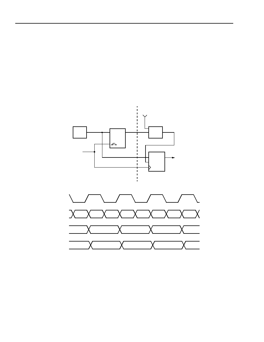
40
Lucent Technologies Inc.
Data Sheet
June 1999
ORCA Series 3C and 3T FPGAs
Programmable Input/Output Cells
(continued)
Input Demultiplexing
The combination of input register capability and the two inputs, IN1 and IN2, from each PIO to the internal routing
provides for input signal demultiplexing without any additional resources. Figure 24 shows the input configuration
and general timing for demultiplexing a multiplexed address and data signal. The PIO input signal is sent to both
the input latch and directly to IN2. The signal is latched on the falling edge of the clock and output to routing at IN1.
The address and data are then both available at the rising edge of the system clock. These signals may be regis-
tered or otherwise processed in the PLCs at that clock edge. Figure 24 also shows the possible use of the SLIC
decoder to perform an address decode to enable which registers are to receive the input data. Although the timing
shown is for using the input register as a latch, it may also be used in the same way as an FF. Also note that the sig-
nals found in PIO inputs IN1 and IN2 can be interchanged.
5-5798(F)
Figure 24. PIO Input Demultiplexing
DEC
D
Q
PAD
PIO
D
Q
CE
SLIC
OTHER ADDRESS
LINES
SCLK
IN1
IN2
SCLK
PIO LATCH
PLC FF
ADDR1
ADDR2
ADDR3
ADDR4
ADDR5
DATA1
DATA2
DATA3
DATA4
DATA1
DATA2
DATA3
ADDR2
ADDR3
ADDR4
ADDR5
DATA0
DATA4
OUTPUT
OUTPUT
PIO INPUT
PLC

Lucent Technologies Inc.
41
Data Sheet
June 1999
ORCA Series 3C and 3T FPGAs
Programmable Input/Output Cells
(continued)
Outputs
The PIC's output drivers have programmable drive
capability and slew rates. Three propagation delays
(fast, slewlim, sinklim) are available on output drivers.
The sinklim mode has the longest propagation delay
and is used to minimize system noise and minimize
power consumption. The fast and slewlim modes allow
critical timing to be met.
The drive current is 12 mA sink/6 mA source for the
slewlim and fast output speed selections and
6 mA sink/3 mA source for the sinklim output. Two adja-
cent outputs can be interconnected to increase the out-
put sink/source current to 24 mA/12 mA.
All outputs that are not speed critical should be config-
ured as sinklim to minimize power and noise. The num-
ber of outputs that switch simultaneously in the same
direction should be limited to minimize ground bounce.
To minimize ground bounce problems, locate heavily
loaded output buffers near the ground pads. Ground
bounce is generally a function of the driving circuits,
traces on the printed-circuit board, and loads and is
best determined with a circuit simulation.
At powerup, the output drivers are in slewlim mode,
and the input buffers are configured as TTL-level com-
patible (CMOS for OR3Txxx) with a pull-up. If an output
is not to be driven in the selected configuration mode, it
is 3-stated.
The output buffer signal can be inverted, and the
3-state control signal can be made active-high, active-
low, or always enabled. In addition, this 3-state signal
can be registered or nonregistered. Additionally, there
is a fast, open-drain output option that directly connects
the output signal to the 3-state control, allowing the out-
put buffer to either drive to a logic 0 or 3-state, but
never to drive to a logic 1. Because there is no explicit
route required to create the open-drain output, its
response is very fast. Like the input side of the PIO,
there are two output connections from PIC routing to
the output side of the PIO, OUT1, and OUT2. These
connections provide for flexible routing and can be
used in data manipulation in the PIO as described in
subsequent paragraphs.
An FF has been added to the output path of the PIO.
The register has a local set/reset and clock enable. The
LSR has the option to be synchronous or asynchro-
nous and have priority set as clock enable over LSR or
LSR over clock enable. Clocking to the output FF can
come from either the system clock or the ExpressCLK
associated with the PIC. The input to the FF can come
from either OUT1 or OUT2, or it can be tied to V
DD
or
GND. Additionally, the input to the FF can be inverted.
Output Multiplexing
The Series 3 PIO output FF can be combined with the
new PIO logic block to perform output data multiplexing
with no PLC resources required. The PIO logic block
has three multiplexing modes: OUT1OUTREG,
OUT2OUTREG, and OUT1OUT2. OUT1OUTREG and
OUT2OUTREG are equivalent except that either OUT1
or OUT2 is MUXed with the FF, where the FF data is
output on the clock phase after the active edge. The
simplest multiplexing mode is OUT1OUT2. In this
mode, the signal at OUT1 is output to the pad while the
clock is low, and the signal on OUT2 is output to the
pad when the clock is high. Figure 25 shows a simple
schematic of a PIO in OUT1OUT2 mode and a general
timing diagram for multiplexing an address and data
signal.
Often an address will be used to generate or read a
data sample from memory with the goal of multiplexing
the data onto a single line. In this case, the address
often precedes the data by one clock cycle.
OUT1OUTREG and OUT2OUTREG modes of the PIO
logic can be used to address this situation.
Because OUT1OUTREG mode is equivalent to
OUT2OUTREG, only OUT2OUTREG mode is
described here. Figure 26 shows a simple PIO sche-
matic in OUT2OUTREG mode and general timing for
multiplexing data with a leading address. The address
signal on OUT1 is registered in the PIO FF. This delays
the address so that it aligns with the data signal. The
PIO logic block then sends the OUTREG signal
(address) to the pad when the clock is high and the
OUT2 signal (data) to the pad when the clock is low,
resulting in an aligned, multiplexed signal.
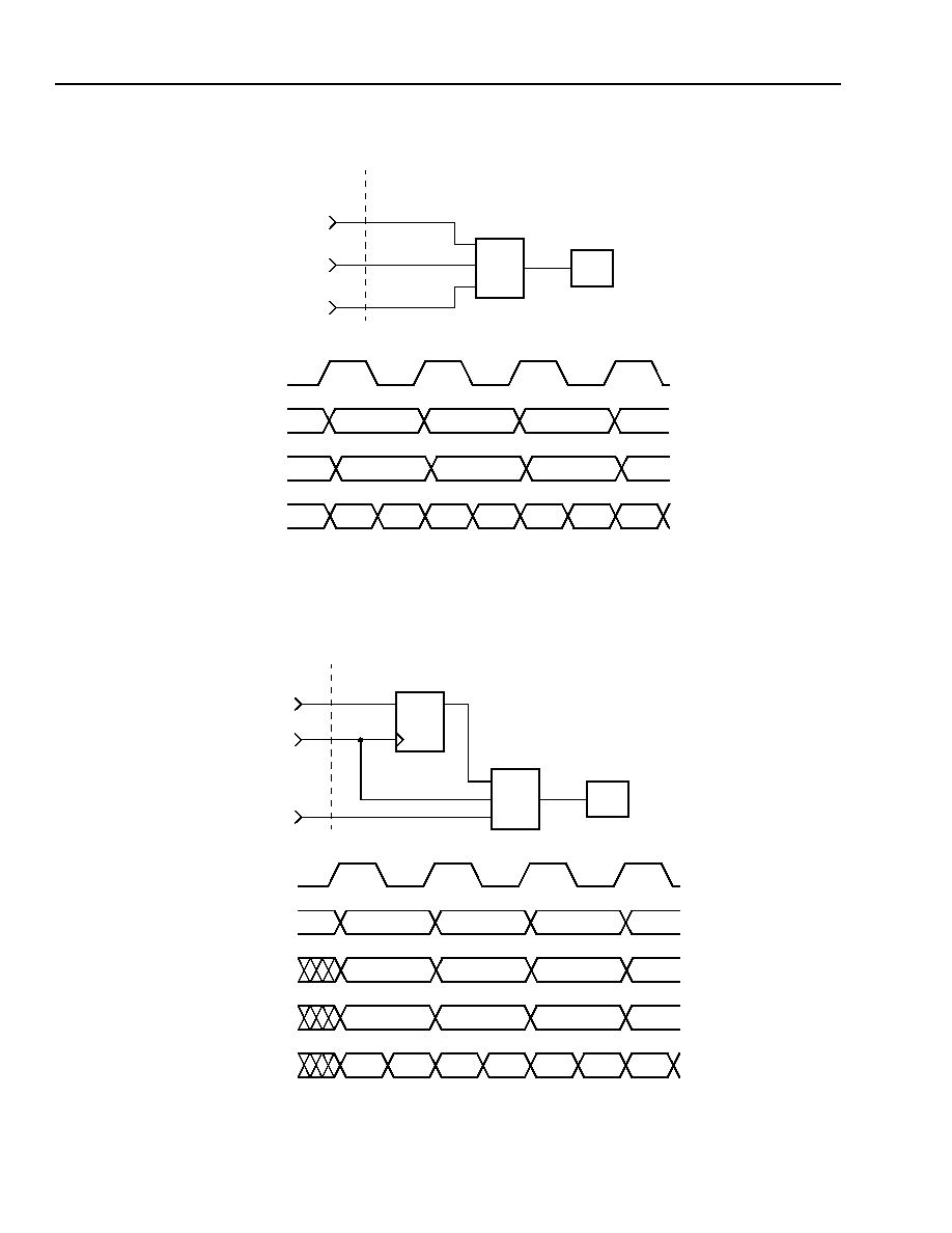
42
Lucent Technologies Inc.
Data Sheet
June 1999
ORCA Series 3C and 3T FPGAs
Programmable Input/Output Cells
(continued)
NOTE: PIO LOGIC MODE, OUT1OUT2
5-5799(F)
Figure 25. Output Multiplexing (OUT1OUT2 Mode)
NOTE: PIO LOGIC MODE, OUT1OUT2
5-5797(F)
Figure 26. Output Multiplexing (OUT2OUTREG Mode)
CLK
ADDR1
ADDR2
ADDR3
ADDR4
ADDR5
DATA2
DATA3
DATA4
DATA5
ADDR1
ADDR2
ADDR3
DATA1
DATA2
DATA3
DATA4
DATA1
ADDR4
OUT1
OUT2
PIC OUTPUT
PLC
ADDRESS
PAD
PIO
LOGIC
OUT1
OUT2
CLK
FROM
ROUTING
DATA
FROM
ROUTING
PIC
PLC
D
Q
CLK
PAD
P/O
LOGIC
OUT1
OUT2
PIC
DATA
CLK
REG ADDRESS
DATA
ADDR1
ADDR2
ADDR3
ADDR4
DATA1
DATA2
DATA3
DATA4
DATA1
DATA2
ADDR1
ADDR2
ADDR3
ADDR4
DATA3
PAD
ADDR ADDR1
ADDR2
ADDR3
ADDR4
ADDR5
FROM
ROUTING
ADDRESS
FROM
ROUTING

Lucent Technologies Inc.
43
Data Sheet
June 1999
ORCA Series 3C and 3T FPGAs
Programmable Input/Output Cells
(continued)
PIO Logic Function Generator
The PIO logic block can also generate logic functions
based on the signals on the OUT2 and CLK ports of
the PIO. The functions are AND, NAND, OR, NOR,
XOR, and XNOR. Table 10 is provided as a summary
of the PIO logic options.
PIO Register Control Signals
As discussed in the Inputs and Outputs subsections,
the PIO latches/FFs have various clock, clock enable
(CE), local set/reset (LSR), and global set/reset
(GSRN) controls. Table 11 provides a summary of
these control signals and their effect on the PIO
latches/FFs. Note that all control signals are optionally
invertible.
Table 10. PIO Logic Options
Option
Description
OUT1OUTREG
Data at OUT1 output when clock
low, data at FF out when clock
high.
OUT2OUTREG
Data at OUT2 output when clock
low, data at FF out when clock
high.
OUT1OUT2
Data at OUT1 output when clock
low, data at OUT2 when clock
high.
AND
Output logical AND of signals on
OUT2 and clock.
NAND
Output logical NAND of signals
on OUT2 and clock.
OR
Output logical OR of signals on
OUT2 and clock.
NOR
Output logical NOR of signals on
OUT2 and clock.
XOR
Output logical XOR of signals on
OUT2 and clock.
XNOR
Output logical XNOR of signals
on OUT2 and clock.
Table 11. PIO Register Control Signals
Control Signal
Effect/Functionality
ExpressCLK
Clocks input fast-capture latch;
optionally clocks output FF, or
3-state FF.
System Clock
(SCLK)
Clocks input latch/FF; optionally
clocks output FF, or 3-state FF.
Clock Enable
(CE)
Optionally enables/disables input
FF (not available for input latch
mode); optionally enables/dis-
ables output FF; separate CE
inversion capability for input and
output.
Local Set/Reset
(LSR)
Option to disable; affects input
latch/FF, output FF, and 3-state
FF if enabled.
Global Set/Reset
(GSRN)
Option to enable or disable per
PIO after initial configuration.
Set/Reset Mode
The input latch/FF, output FF, and
3-state FF are individually set or
reset by both the LSR and GSRN
inputs.

44
44
Lucent Technologies Inc.
Data Sheet
June 1999
ORCA Series 3C and 3T FPGAs
Programmable Input/Output Cells
(continued)
PIC Routing Resources
The PIC routing borrows many of the concepts and
constructs from the PLC routing. It is designed to be
able to gather an 8-bit bidirectional bus from any eight
consecutive I/O pads and route them to either or both
of the two adjacent PLCs. The eight I/O bits do not
need to start at a PIC boundary; that is, they may start
at one of the middle two PIOs in a PIC and span three
PICs.
Substantial routing has been added to the PIC to off-
load PLC routing from being used to move signals
around the PLC array perimeter. This saves PLC rout-
ing for logic purposes and provides greater flexibility for
locking design pinouts prior to final placement and rout-
ing of the device, or allowing a change in the pinout late
in the design cycle. The PIC routing has also been
increased substantially to allow routing to the complex
PIO cells that now allow multiple inputs and outputs per
device pin, along with new sequential control signals,
such as clock enable, LSR, and clock.
PICs are grouped in pairs for purposes of discussing
PIC routing. On the sides of a device, the PICs in a pair
are referred to as top and bottom. On the top or bottom
of a device, the PICs in a pair are referred to as left or
right. For example, on the top edge of the device, the
leftmost PIC, PT1, is the left PIC of a pair, and PIC PT2
is the right PIC of that pair. The next PIC to the right,
PT3, is the left PIC of the next pair, and so on.
The need for PIC pairs stems from the routing of
switching segments and PLC half- and long-line driv-
ers. As described below, the connectivity for these
types of routing is grouped across pairs of PICs to pro-
vide complete and fast routing of I/O signals between a
given PIC and the three adjacent PLCs: one orthogonal
and two diagonal.
PIC routing segments use the same terminology as
PLC routing segments, but are prefixed with a p to dis-
tinguish them as belonging to the PICs.
PIC Switching Segments. Each PIC has two groups
of switching segments (pSW), each group having eight
lines with connectivity to the PIOs in groups of four.
One set of switching segments connects to the PIC to
the left (above), and the other set connects to the
switching segments of the PIC to the right (below). This
means of connectivity between PICs using staggered
connections of groups of switching segments allows a
given PIC to route signals to both adjacent PICs and all
adjacent PLCs efficiently. This provides single signal
routing flexibility and routing of multiple buses on
groups of I/Os without tying up global routing
resources.
px1 Routing Segments. There are five px1 routing
segments in each PIC that run parallel to the edge of
the chip on which the PIC resides, each broken by a
CIP in each PIC. The px1 segments have connectivity
to the pSW segments and to the x1 routing segments
of the two adjacent PLCs.
px2 Routing Segments. There are five px2 routing
segments in each PIC that run parallel to the edge of
the chip on which the PIC resides. To provide greater
routing flexibility, the CIPs that break the px2 segments
every two PICs are staggered across the two PICs in a
pair. One PIC of the pair has break CIPs on the even-
numbered px2 segments, and the other has them on
the odd-numbered px2 segments. The px2 segments
have connectivity to the pSW segments and to the x1
routing segments of the two adjacent PLCs.
px5 Routing Segments. There are ten px5 routing
segments in each PIC that run parallel to the edge of
the chip on which the PIC resides. Two of the ten seg-
ments are broken in each PIC so that each segment is
broken every five PICs. All ten px5 segments break at
the corners of the chip, allowing independent px5 rout-
ing on each edge of the chip. The px5 routing seg-
ments connect to the pSW segments and the x5 and
xH routing segments of the two adjacent PLCs.
pxH Routing Segments. Each PIC contains eight pxH
routing segments that run parallel to the edge of the
chip on which the PIC resides. The pxH segments have
connectivity with the xL, xH, and one set of xBID rout-
ing segments in the immediately adjacent PLC.
pxL Routing Segments. There are ten pxL routing
segments in each PIC that run parallel to the edge of
the chip on which the PIC resides. Each of the xL lines
makes a connection to an xL line from the adjacent
PLC. PIC long lines (xL) can be used for global signal
distribution just as PLC xL lines can.

Lucent Technologies Inc.
45
Data Sheet
June 1999
ORCA Series 3C and 3T FPGAs
Programmable Input/Output Cells
(continued)
PIC Architectural Description
The PIC architecture as seen in
ORCA
Foundry is
shown in Figure 27. The figure is the left PIC of a PIC
pair on the top edge of a Series 3 array. Both PICs in a
pair are similar, with the differences mainly lying in the
connections between the PIC switching segments
(pSW), the IN2 connections across PIC boundaries,
and the system clock spine driver residing in only one
PIC of a pair.
A. This is a programmable input/output (PIO). There
are four PIOs per PIC. The PIOs contain the PIC
logic and I/O buffers.
B. This is the PIC output switching block. It connects
the PIC switching segments and local clock lines to
the PIO output and control signals.
C. This is the system clock spine switching block and
buffer. There is only one system clock spine per pair
of PICs. Its inputs can come from the PIC switching
segments or any of the eight PIO inputs in a PIC
pair.
D. PIC switching segments (pSW). These routing seg-
ments are used to interconnect routing resources
within the PIC and to a lesser degree, between
PICs.
E. px1 routing segments. The PIC x1 routing seg-
ments traverse one PIC and break at a CIP in the
middle of each PIC.
F. px2 routing segments. The PICs have routing that
traverses two PICs between breaks. The breaks are
staggered among the five px2 segments.
G. px5 routing segments. Each of the ten PIC x5 rout-
ing segments traverses five PICs in between breaks
at a CIP. Two px5 segments break in each PIC.
H. pxH routing segments. The eight PIC xH routing
segments traverse half of the array and break at
CIPs in the interquad routing region that is in the
middle of the array.
I.
(Not used intentionally for clarity.)
J. pxL routing segments. The PIC long lines run the
entire length of the side of the array.
K. x5 routing segments from the adjacent PLC routing.
L. xL routing segments from the adjacent PLC routing.
M. x1 routing segments from the adjacent PLC routing.
N. Switching segments from the adjacent PLC routing.
O. xH routing segments from the adjacent PLC routing.
P. BIDI routing segments from the adjacent PLC rout-
ing.
Q. These are the IN2 routing segments. There is one
IN2 line from each PIO, and all eight IN2 lines from
each PIC pair are present in both PICs of a pair.
R. These CIPs connect the IN1 and IN2 routing seg-
ments from the PIOs to the PIC switching seg-
ments.
S. These CIPs break the PIC switching segments at
the interface between a PIC pair.
T. These CIPs connect adjacent PLC routing
resources to the PIC switching segments.
U. These CIPs connect inter-PIC routing with the PIC
switching segments.
V. These CIPs break the px1, px2, and px5 routing at
the middle of a PIC. The px2 and px5 CIP place-
ment varies depending on the PLC.
W. These mutually exclusive buffers can drive one long
line signal onto a PIC local clock routing segment.
X. These mutually exclusive buffers can select a
source from one of the local system clock routes to
drive the PIO 3-state control signal.
Y. These are the four local system clock routing seg-
ments. Two come from connections within the PIC,
one from the other PIC in the pair, and one from the
adjacent PLC.
Z. These mutually exclusive buffers allow a signal on
the PIC switching segments to be routed to a sys-
tem clock spine or to a PIO system clock.
AA. ExpressCLK routing line.
AB. System clock spine.
AC. These various groups of CIPs connect routing
resources from the adjacent PLC to the inter-PIC
routing resources.
AD. These buffers provide connectivity between the
PLC xL (xH) lines and the PIC xL (xH) lines or
connectivity between one of the IN2 routing seg-
ments and the PIC and/or PLC xL (xH) routing
segments.
AE. These mutually exclusive buffers and CIPs provide
connectivity to the PLC xL and xH lines from one
of the IN2 input segments.
AF. These buffers allow the IN2 signals to drive onto
the BIDI routing of the adjacent PLC, or the BIDI
routing of the adjacent PLC, and the PIC switching
segments and/or PIC half lines may be connected.
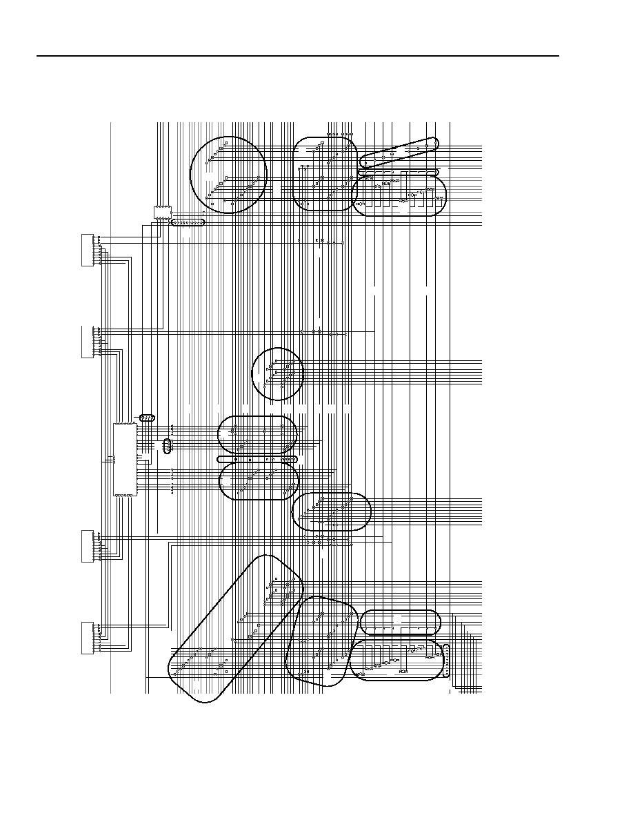
46
Lucent Technologies Inc.
Data Sheet
June 1999
ORCA Series 3C and 3T FPGAs
Programmable Input/Output Cells
(continued)
5-5823(F)
Figure 27. PIC Architecture
AA
AA
AA
B
Y
D
D
D
D
E
F
H
J
Z
X
AC
G
AE
AD
T
W
R
T
V
U
U
AC
J
Q
Q
R
R
C
P
O
N
M
AD
M
K
L
K
S
AF
W
T
H
AE
AC
AB
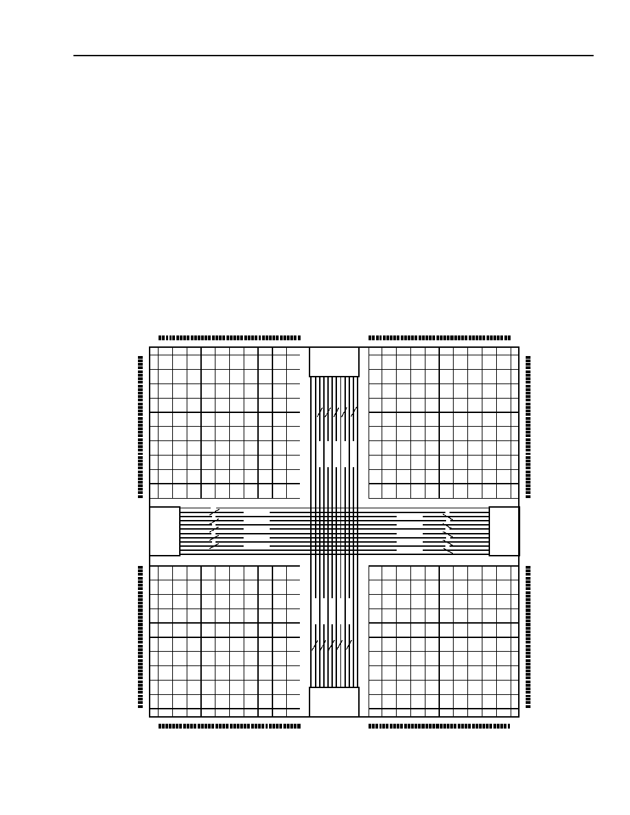
Lucent Technologies Inc.
47
Data Sheet
June 1999
ORCA Series 3C and 3T FPGAs
High-Level Routing Resources
The high-level routing resources in the
ORCA
Series 3 devices are interquad routing, corner cell routing, and PIC
interquad routing. These resources and their related structures are discussed in the following subsections.
Interquad Routing
In the
ORCA
Series 3 devices, the PLC array is split into four equal quadrants. In between these quadrants, routing
has been added to route signals between the quadrants and distribute clocks. In addition to general routing, there
are four specialized clock routing spines. The general routing is discussed below, followed by the special clock rout-
ing.
One of the main purposes of interquad routing is to distribute internally generated signals, such as clocks and con-
trol signals. There are two types of interquad blocks: vertical and horizontal. Vertical interquad blocks (vIQ) run
between quadrants on the left and right, while horizontal interquad blocks (hIQ) run between top and bottom quad-
rants. Interquad lines begin and end in the MID cells that are discussed later. Since hIQ and vIQ blocks have the
same logic, only the hIQ block is described below. The interquad routing connects to x5 and xH segments. It does
not affect other local routing (xsw, x1, fast carry), so local routing is the same, whether PLC-PLC connections cross
quadrants or not. Figure 28 presents a (not to scale) view of interquad routing.
5-4538(F)
Figure 28. Interquad Routing
TMID
BMID
5
5
5
5
vIQ2
[4:0]
vIQ4
[4:0]
vIQ6
[4:0]
vIQ8[4
:0]
vIQ0[4
:0]
vIQ3
[4:0]
vIQ5
[4:0]
vIQ7
[4:0]
vIQ9[4
:0]
vIQ1[4
:0]
5
5
5
5
5
5
LMID
RMID
hIQ7[4:0]
hIQ5[4:0]
hIQ3[4:0]
hIQ1[4:0]
hIQ9[4:0]
hIQ6[4:0]
hIQ4[4:0]
hIQ2[4:0]
hIQ0[4:0]
hIQ8[4:0]
5
5
5
5
5
5
5
5
5
5
FAST CLOCK R
FAST CLOCK L
F
A
S
T
CL
OCK
T
F
AST
CL
O
C
K B

48
48
Lucent Technologies Inc.
Data Sheet
June 1999
ORCA Series 3C and 3T FPGAs
High-Level Routing Resources
(continued)
Figure 29 shows the connections from the interquad
routing to the inter-PLC routing for a block of the hori-
zontal interquad. The vertical interquad has similar
connections. The connections shown in Figure 29 are
made with PLCs located above and below the routing
shown in the figure. The interquad routing segments,
prefixed IH for interquad horizontal, are in ten groups of
five lines. Any one line from each group can be routed
to one of the xH segments from the top of the device
(left for vertical interquad), one of the xH segments
from the bottom of the device (right for vertical inter-
quad), and one of the x5 segments crossing the inter-
quad.
Figure 28 shows four fast middle clock (fast clock) sig-
nals with the suffixes T (top), B (bottom), R (right), and
L (left), respectively. Figure 29 also shows the fast
clock R and fast clock L lines; these are dedicated
interquad clock spines. They originate in the CLKCN-
TRL special function blocks in the middle of each edge
of the device, with the name referencing the edge of
origin. For example, fast clock R originates in the
CLKCNTRL block on the right edge of a device. Fast
clock spines traverse the entire PLC array but do not
connect to the PICs on the edge of the device opposite
to the source. Each fast clock line connects to two of
the xL lines in each PLC that run orthogonally to the
fast clock. These connections allow the fast clock lines
to generate a clock tree that can reach any PLC in the
device. Fast clocks and other clock resources are dis-
cussed in the Clock Distribution Network section.
Programmable Corner Cell Routing
Programmable Routing
The programmable corner cell (PCC) contains the cir-
cuitry to connect the routing of the two PICs in each
corner of the device. The PIC px1 and px2 segments
and eight PIC switching segments are directly con-
nected together from one PIC to another. The px5 lines
are all broken with CIPs and the PIC pxL and pxH
segments are connected from one block to another
through programmable buffers.
Corner Cell Special Functions
In addition to routing functions, special-purpose func-
tions are located in each FPGA corner. The upper-left
PCC contains connections to the boundary-scan logic
and microprocessor interface. The upper-right PCC
contains connections to the readback logic, connectiv-
ity to the global 3-state signal (TS_ALL), and a pro-
grammable clock manager. The lower-left PCC
contains connections to the internal oscillator and a
programmable clock manager. The lower-right PCC
contains connections to the start-up and global reset
logic. These functions are all more completely
described in the Special Function Blocks section of this
data sheet.
5-5821(F)
Figure 29. hIQ Block Detail
IH 0[4:0]
IH 1[4:0]
IH 2[4:0]
IH 3[4:0]
IH 4[4:0]
F A S T C LO C K R
IH 5[4:0]
IH 6[4:0]
IH 7[4:0]
IH 8[4:0]
IH 9[4:0]
F A S T C LO C K L
B L[9:0] vxL[9:0] vx5[9:0] vx1[9:0]
S U L[9:0]
vx1[9:0]
vxH [9:0] B L[9:0]
F A S T
vck
C A R R Y
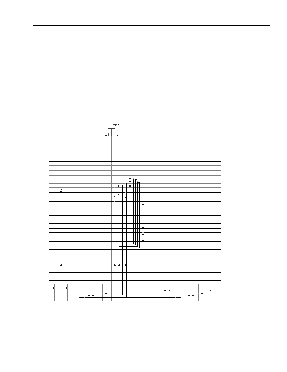
Lucent Technologies Inc.
49
Data Sheet
June 1999
ORCA Series 3C and 3T FPGAs
High-Level Routing Resources
(continued)
PIC Interquad (MID) Routing
There is also connectivity between the PICs in each
quadrant, as well as a clock control (CLKCNTRL) mod-
ule (discussed in the Special Function Blocks section)
between the PIC routing and the interquad routing.
These blocks are called LMID (left), TMID (top), RMID
(right), and BMID (bottom). The TMID routing is shown
in Figure 30. As with the hIQ and vIQ blocks, the only
connectivity to the PIC routing is to the global pxH and
px5 segments.
The pxH segments from the one quadrant can be con-
nected through a CIP to its counterpart in the opposite
quadrant, providing a path that spans the array of
PICs. Since a passive CIP is used to connect the two
pxH segments, a 3-state signal can be routed on the
two pxH segments in the opposite quadrants, and then
connected through this CIP. As with the hIQ and vIQ
blocks, CIPs and buffers allow nibble-wide connections
between the interquad segments, the xH segments,
and the x5 segments.
5-5822(F)
Figure 30. Top (TMID) Routing
EXPRESSCLK RIGHT
PIC LOCAL CLOCKS
PIC LOCAL CLOCKS
pxL[9:0]
pxH[7:0]
px5[9:0]
px1[4:0]
pSW[7:4]
pSW[3:0]
pSW[7:4]
pSW[3:0]
px2[4:0]
1v
9x
L
[
4]
1v
8x
L
[
3]
I
v
7x
L
[
2]
FA
S
T
CL
O
C
K
I
v
7x
L
[
0]
I
v
6x
L
[
3]
I
v
6x
L
[
1]
I
v
5x
L
[
2]
I
v
5x
L
[
0]
I
v
4x
L
[
3]
I
v
3x
L
[
3]
I
v
3x
L
[
1]
I
v
2x
L
[
2]
I
v
2x
L
[
0]
I
v
1x
L
[
3]
I
v
1x
L
[
1]
1v
0x
L
[
2]
1v
0x
L
[
0]
Iv4
xL
1
]
in2[A:D] FROM LEFT
in[A:D] FROM RIGHT
CORNER ExpressCLK
FROM RIGHT
FROM LEFT
EXPRESSCLK LEFT
SHUTOFF
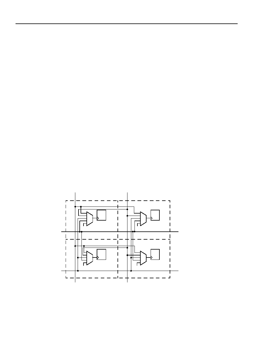
50
50
Lucent Technologies Inc.
Data Sheet
June 1999
ORCA Series 3C and 3T FPGAs
Clock Distribution Network
The Series 3 FPGAs provide three types of high-
speed, low-skew clock distributions: system clock, fast
middle clock (fast clock), and ExpressCLK. Because of
the great variety of sources and distribution for clock
signals in the
ORCA
Series 3, the clock mechanisms
will be described here from the inside out. The clock
connections to the PFU will be described, followed by
clock distribution to the PLC array, clock sources to the
PLC array, and finally ending with clock sources and
distribution in the PICs. The ExpressCLK inputs are
new, dedicated clock inputs in Series 3 FPGAs. They
are mentioned in several of the clock network descrip-
tions and are described fully later in this section.
PFU Clock Sources
Within a PLC there are five sources for the clock signal
of the latches/FFs in the PFU. Two of the signals are
generated off of the long lines (xL) within the PLC: one
from the set of vertical long lines and one from the set
of horizontal long lines. For each of these signals, any
one of the ten long lines of each set, vertical or horizon-
tal, can generate the clock signal. Two of the five PFU
clock sources come from neighboring PLCs. One clock
is generated from the PLC to the left or right of the cur-
rent PLC, and one is generated from the PLC above or
below the current PLC. The selection decision as to
where these signals come from, above/below and left/
right, is based on the position of the PLC in the array
and has to do with the alternating nature of the source
of the system clock spines (discussed later). The last of
the five clock sources is also generated within the PLC.
The E1 control signal, described in the PLC Routing
Resources section, can drive the PFU clock. The E1
signal can come from any xBID routing resource in the
PLC. The selection and switching of clock signals in a
PLC is performed in the FINS. Figure 31 shows the
PFU clock sources for a set of four adjacent PLCs.
Global Control Signals
The four clock signals in each PLC that are generated
from the long lines (xL) in the current PLC or an adja-
cent PLC can also be used to drive the PFU clock
enable (CE), local set/reset (LSR) and add/subtract/
write enable (ASWE) signals. The clock signals gener-
ated from vertical long lines can drive CE and ASWE,
and the clocks generated from horizontal long lines can
drive LSR. This allows for low-skew global distribution
of two of these three control signals with the clock rout-
ing while still allowing a global clock route to occur.
5-6054(F)
Figure 31. PFU Clock Sources
PFU
PLC
PFU
PLC
PFU
PLC
PFU
PLC
E1
E1
E1
E1
hxL[9:0]
hxL[9:0]
vxL[9:0]
vxL[9:0]
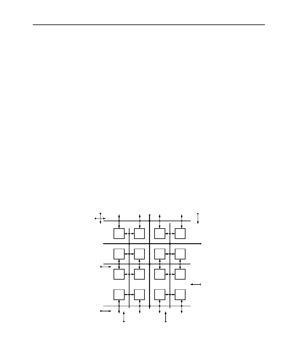
Lucent Technologies Inc.
51
Data Sheet
June 1999
ORCA Series 3C and 3T FPGAs
Clock Distribution Network
(continued)
Clock Distribution in the PLC Array
System Clock (SCLK)
The clock distribution network, or clock spine network,
within the PLC array is designed to minimize clock skew
while maximizing clock flexibility. Clock flexibility is
expressed in two ways: the ease with which a single
clock is routed to the entire array, and the capability to
provide multiple clocks to the PLC array.
There is one horizontal and one vertical clock spine
passing through each PLC. The horizontal clock spine
is sourced from the PIC in the same row on either the
left- or right-hand side of the array, with the source side
(left or right) alternating for each row. The vertical clock
spines are similarly sourced from the PICs alternating
from the top or bottom of a column. Each clock spine is
capable of driving one of the ten xL routing segments
that run orthogonal to it within each PLC. Full connec-
tivity to all PFUs is maintained due to the connectivity
from the xL lines to the PFU clock signals described in
the previous section; however, only an xL line in every
other row (column) needs to be driven to allow the
given clock signal to be distributed to every PFU.
Figure 32 is a high-level diagram of the Series 3 system
clock spine network with sample xL line
connections for a 4 x 4 array of PLCs.
The clock spine structure previously described pro-
vides for complete distribution of a clock from any I/O
pin to the entire PLC array by means of a single clock
spine and long lines (xL). This distribution system also
provides a means to have many different clocks routed
to many different and dispersed locations in the PLC
array. Each spine can carry a different clock signal, so
for the OR3C/T55 (which has an 18 x 18 array of PLCs,
implying nine clock spines per side), 36 input clock sig-
nals can be supported using the system clock network.
Fast Clock
Fast clocks are high-speed, low-skew clock spines that
originate from the CLKCNTRL special function blocks
(described later). There are four fast clock spines--one
originating on the middle of each edge of the array. The
spines run in the interquad region of the PLC array
from their source side of the device to the last row or
column on the opposite side of the device. The fast
clocks connect to two long lines, xL[8] and xL[9], that
run orthogonal to the spine direction in each PLC.
These long lines can then be connected to the PFU
clock input in the same manner as the general system
clocks, and, like the system clock connections, xL lines
are only needed in every other row (column) to distrib-
ute a clock to every PFU. The limited number of long-
line connections and the low skew of the CLKCNTRL
source combine to make the fast clocks a very robust,
low-skew clock source.
5-5801(F).a
Figure 32.
ORCA
Series 3 System Clock Distribution Overview
(xL)
HORIZONTAL
(xL)
UNUSED
(xL)
(xL)
UNUSED
SCLK SPINE
(xL)
UNUSED
SCLK SPINE
VERTICAL
SCLK SPINE
SCLK SPINE
SCLK SPINE
UNUSED
SCLK SPINE
UNUSED
SCLK SPINE
UNUSED
SCLK SPINE
UNUSED
SCLK SPINE
UNUSED
SCLK SPINE
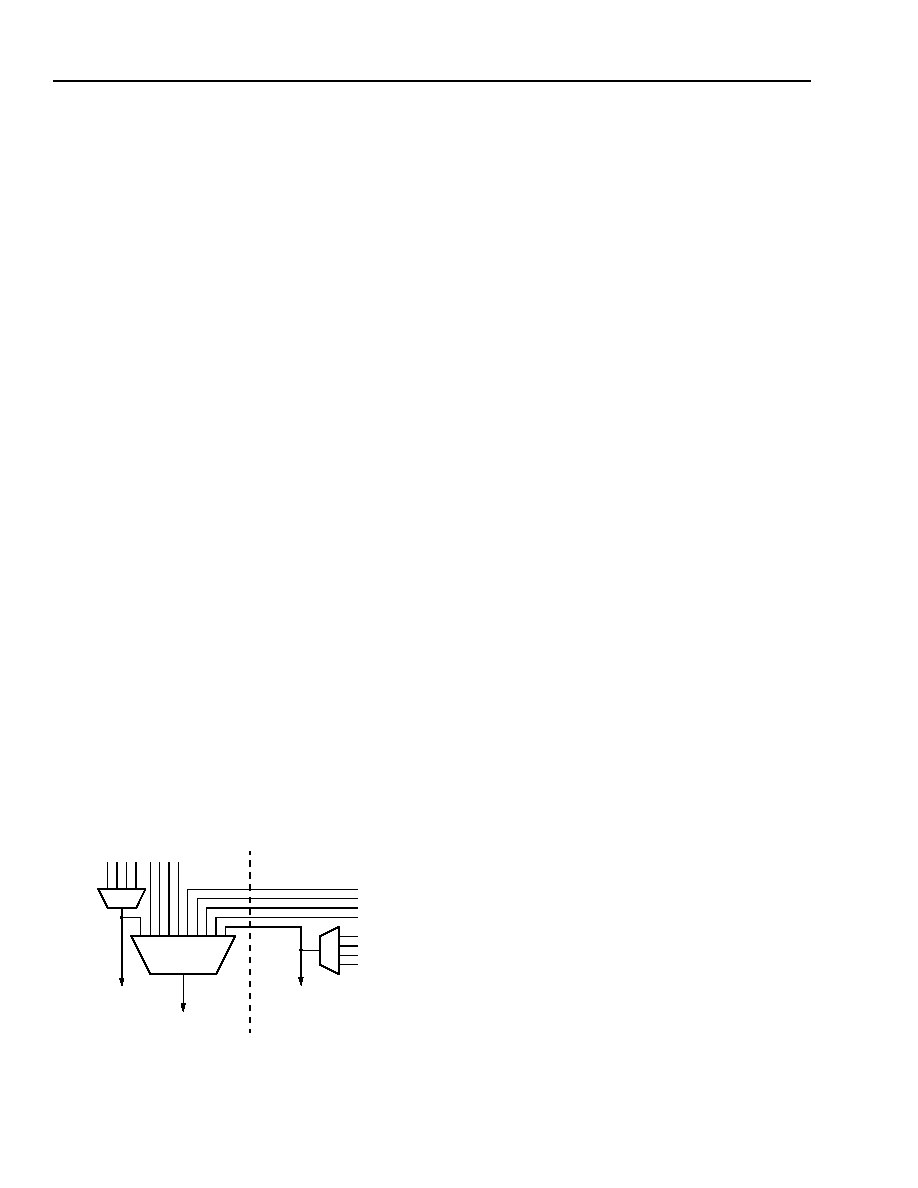
52
52
Lucent Technologies Inc.
Data Sheet
June 1999
ORCA Series 3C and 3T FPGAs
Clock Distribution Network
(continued)
Clock Sources to the PLC Array
The source of a clock that is globally available to the
PLC array can be from any user I/O pad, any of the
ExpressCLK
pads, or an internally generated source.
System Clock
As described in the Programmable Input/Output Cells
section, PICs are grouped in adjacent pairs. Any one of
the eight pads in a PIC pair can drive a clock spine in a
row or column. For PIC pairs on the top of the chip, the
column associated with the left PIC has the clock
spine, for pairs on the bottom, the right PIC column has
the spine. The top PIC of the pair sources the spine
from the left side of the array, and the bottom PIC of the
pair sources the spine from the right side of the array.
Clock delay and skew are minimized by having a single
clock buffer per pair of PICs. The clock spine for each
pair can also be driven by one of the four PIC switching
segments (pSW) in each PIC of the pair. This allows a
signal generated in the PLC array to be routed onto the
global clock spine network. The system clock output of
the programmable clock manager (PCM) may also be
routed to the global system clock spines via the pSW
segments. Figure 33 shows the clock spine multiplex-
ing structure for a pair of PICs on the top of the array.
Fast Clock
The fast clock spines are sourced to the PLC array
from each side of the device by the ExpressCLK pads
via the CLKCNTRL function block (described in the
Special Function Blocks section). The ExpressCLK and
fast clock source from the pads is shown in Figure 34
and will be described further in the ExpressCLK Inputs
subsection.
5-5800(F)
Figure 33. PIC System Clock Spine Generation
Clocks in the PICs
Because the Series 3 FPGAs have latches and FFs in
the I/Os, it is necessary to have clock signal distribution
to the PIOs as well as in the PLC array. The system
clock, the fast clock, and the ExpressCLK are available
for PIO clocking.
PIC System Clock
There are five local system clock lines in each PIC.
Much like the sources for a clock in the PFU, two of the
local PIC clocks are generated within the PIC from long
lines. One is generated from the set of ten PIC long
lines (pxL) that runs parallel to the PICs on a side, and
the other is generated from the set of ten long lines (xL)
from the PLC array that terminate in the PIC. Another
local PIC system clock route comes from the set of ten
xL lines in the adjacent PLC that is parallel to the side
of the array on which the PIC resides. The fourth local
PIC system clock route comes from the set of ten long
lines (xL) from the PLC array that terminate in the adja-
cent PIC that is not part of the same PIC pair. Much like
the E1 signals in the PLCs that are used to distribute a
local clock to the PFU source, the fifth local clock line in
each PIC comes from local pSW signals. This clock
signal for each PIC is shown in Figure 33. One of these
five local PIC system clocks is selected for the system
clock signal in the PIO. It is used as the PIO system
clock for both input and output clocking as selected
within the PIO. All PIOs in a PIC share the same sys-
tem clock.
PIC ExpressCLK
The ExpressCLK signal used at the PIC latches/FFs
comes from the CLKCNTRL function block that resides
in the middle of the side on which the PIC resides. A
single signal comes from the CLKCNTRL and is driven
by separate buffers onto two ExpressCLK long wires.
One of these ExpressCLK signals goes to the PICs on
the right of (above) the CLKCNTRL block, and the
other ExpressCLK signal goes to the PICs on the left of
(below) the CLKCNTRL block on that side.
PAD A
PAD B
PAD C
PAD D
pSW[4]
pSW[5]
pSW[6]
pSW[7]
PA
D
A
PA
D
B
PAD
C
PA
D
D
pS
W
[
4]
pS
W
[
5]
pS
W
[
6]
pS
W
[
7]
SPINE
TO LOCAL CLOCKS
TO LOCAL CLOCKS
TPICL
TPICR
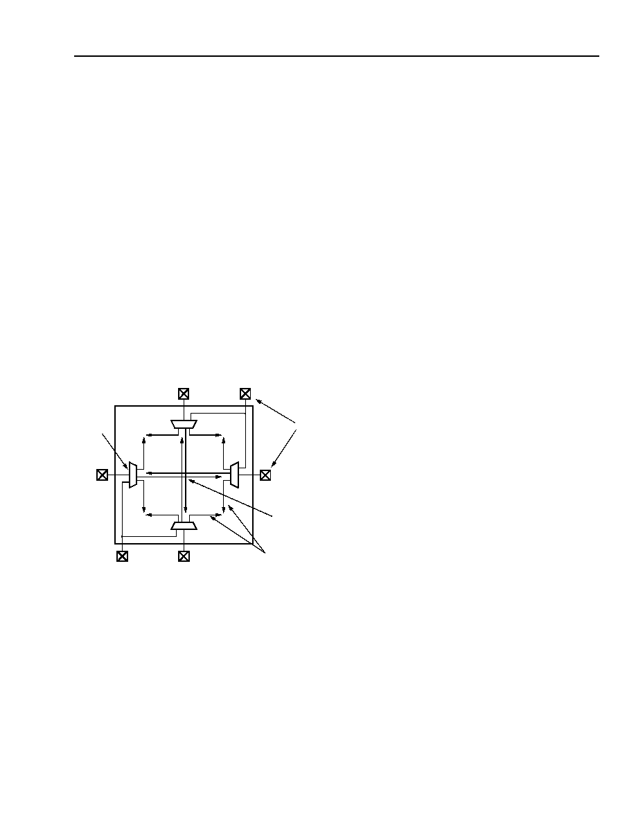
Lucent Technologies Inc.
53
Data Sheet
June 1999
ORCA Series 3C and 3T FPGAs
Clock Distribution Network
(continued)
ExpressCLK Inputs
There are four dedicated ExpressCLK pads on each
Series 3 device: one in the middle of each side. Two
other user I/O pads can also be used as corner
ExpressCLK
inputs, one on the lower-left corner, and
one on the upper-right corner. The corner ExpressCLK
pads feed the ExpressCLK to the two sides of the array
that are adjacent to that corner, always driving the
same signal in both directions. The ExpressCLK route
from the middle pad and from the corner pad associ-
ated with that side are multiplexed and can be glitch-
lessly stopped/started under user control using the
StopCLK
feature of the CLKCNTRL function block
(described under Special Function Blocks) on that side.
The ExpressCLK output of the programmable clock
manager (PCM) is programmably connected to the cor-
ner ExpressCLK routes. PCM blocks are found in the
same corners as the corner ExpressCLK signals and
are described in the Special Function Blocks section.
The ExpressCLK structure is shown in Figure 34 (PCM
blocks are not shown).
5-5802(F)
Note: All multiplexers are set during configuration.
Figure 34. ExpressCLK and Fast Clock Distribution
Selecting Clock Input Pins
Any user I/O pin on an
ORCA
FPGA can be used as a
fast, low-skew system clock input. Since the four dedi-
cated ExpressCLK inputs can only be used to distribute
global signals into the FPGA, these pins should be
selected first as clock pins. Within the interquad region
of the device, these clocks sourced by the ExpressCLK
inputs are called fast clocks. Choosing the next clock
pin is completely arbitrary, but using a pin that is near
the center of an edge of the device will provide the low-
est skew system clock network. The pin-to-pin timing
numbers in the Timing Characteristics section assume
that the clock pin is in one of the PICs at the center of
any side of the device next to an ExpressCLK pad. For
actual timing characteristics for a given clock pin, use
the timing analyzer results from
ORCA
Foundry.
To select subsequent clock pins, certain rules should
be followed. As discussed in the Programmable Input/
Output Cells section, PICs are grouped into adjacent
pairs. Each of these pairs contains eight I/Os, but only
one of the eight I/Os in a PIC pair can be routed directly
onto a system clock spine. Therefore, to achieve top
performance, the next clock input chosen should not be
one of the pins from a PIC pair previously used for a
clock input. If it is necessary to have a second input in
the same PIC pair route onto global system clock rout-
ing, the input can be routed to a free clock spine using
the PIC switching segment (pSW) connections to the
clock spine network at some small sacrifice in speed.
Alternatively, if global distribution of the secondary
clock is not required, the signal can be routed on long
lines (xL) and input to the PFU clock input without
using a clock spine.
Another rule for choosing clock pins has to do with the
alternating nature of clock spine connections to the xL
and pxL routing segments. Starting at the left side of
the device, the first vertical clock spine from the top
connects to hxL[0] (horizontal xL[0]), and the first verti-
cal clock spine from the bottom connects to hxL[5] in all
PLC rows. The next vertical clock spine from the top
connects to hxL[1], and the next one from the bottom
connects to hxL[6]. This progression continues across
the device, and after a spine connects to hxL[9], the
next spine connects to hxL[0] again. Similar connec-
tions are made from horizontal clock spines to vxL (ver-
tical xL) lines from the top to the bottom of the device.
Because the
ORCA
Series 3 clock routing only
requires the use of an xL line in every other row or col-
umn, even two inputs chosen 20 PLCs apart on the
same xL line will not conflict, but it is always better to
avoid these choices, if possible. The fast clock spines
in the interquad routing region also connect to xL[8]
and xL[9] for each set of xL lines, so it is better to avoid
user I/Os that connect to xL[8] or xL[9] when a fast
clock is used that might share one of these connec-
tions. Another reason to use the fast clock spines is
that since they use only the xL[9:8] lines, they will not
conflict with internal data buses which typically use
xL[7:0]. For more details on clock selection, refer to
application notes on clock distribution in
ORCA
Series
3 devices.
EX PR ES SC LKS TO PIO s
FAST C LO C KS
E XPR ES SC LK PAD S
C LKC N TR L
B LOC K
54
54
Lucent Technologies Inc.
Data Sheet
June 1999
ORCA Series 3C and 3T FPGAs
Special Function Blocks
Special function blocks in the Series 3 provide extra
capabilities beyond general FPGA operation. These
blocks reside in the corners and MIDs (middle inter-
quad areas) of the FPGA array.
Single Function Blocks
Most of the special function blocks perform a specific
dedicated function. These functions are data/configura-
tion readback control, global 3-state control (TS_ALL),
internal oscillator generation, global set/reset (GSRN),
and start-up logic.
Readback Logic
The readback logic is located in the upper right corner
of the FPGA and can be enabled via a bit stream option
or by instantiation of a library readback component.
Readback is used to read back the configuration data
and, optionally, the state of the PFU outputs. A read-
back operation can be done while the FPGA is in nor-
mal system operation. The readback operation cannot
be daisy-chained. To use readback, the user selects
options in the bit stream generator in the
ORCA
Foundry Development System.
Table 12 provides readback options selected in the bit
stream generator tool. The table provides the number
of times that the configuration data can be read back.
This is intended primarily to give the user control over
the security of the FPGA's configuration program. The
user can prohibit readback (0), allow a single readback
(1), or allow unrestricted readback (U).
Readback can be performed via the Series 3 micropro-
cessor interface (MPI) or by using dedicated FPGA
readback controls. If the MPI is enabled, readback via
the dedicated FPGA readback logic is disabled. Read-
back using the MPI is discussed in the Microprocessor
Interface (MPI) section.
The pins used for dedicated readback are readback
data (RD_DATA), read configuration (
RD_CFG
), and
configuration clock (CCLK). A readback operation is ini-
tiated by a high-to-low transition on
RD_CFG
. The
RD_CFG
input must remain low during the readback
operation. The readback operation can be restarted at
frame 0 by driving the
RD_CFG
pin high, applying at
least two rising edges of CCLK, and then driving
RD_CFG
low again. One bit of data is shifted out on
RD_DATA at the rising edge of CCLK. The first start bit
of the readback frame is transmitted out several cycles
after the first rising edge of CCLK after
RD_CFG
is input
low (see the Readback Timing Characteristics table in
the Timing Characteristics section). To be certain of the
start of the readback frame, the data can be monitored
for the 01 frame start bit pair.
Readback can be initiated at an address other than
frame 0 via the new microprocessor interface (MPI)
control registers (see the Microprocessor Interface
(MPI) section for more information). In all cases, read-
back is performed at sequential addresses from the
start address.
It should be noted that the RD_DATA output pin is also
used as the dedicated boundary-scan output pin, TDO.
If this pin is being used as TDO, the RD_DATA output
from readback can be routed internally to any other pin
desired. The
RD_CFG
input pin is also used to control
the global 3-state (TS_ALL) function. Before and during
configuration, the TS_ALL signal is always driven by
the
RD_CFG
input and readback is disabled. After con-
figuration, the selection as to whether this input drives
the readback or global 3-state function is determined
by a set of bit stream options. If used as the
RD_CFG
input for readback, the internal TS_ALL input can be
routed internally to be driven by any input pin.
Table 12. Readback Options
Option
Function
0
Prohibit Readback
1
Allow One Readback Only
U
Allow Unrestricted Number of Readbacks

Lucent Technologies Inc.
55
Data Sheet
June 1999
ORCA Series 3C and 3T FPGAs
Special Function Blocks
(continued)
The readback frame contains the configuration data
and the state of the internal logic. During readback, the
value of all registered PFU and PIC outputs can be
captured. The following options are allowed when
doing a capture of the PFU outputs.
1. Do not capture data (the data written to the RAMs,
usually 0, will be read back).
2. Capture data upon entering readback.
3. Capture data based upon a configurable signal
internal to the FPGA. If this signal is tied to
logic 0, capture RAMs are written continuously.
4. Capture data on either options 2 or 3 above.
The readback frame has an identical format to that of
the configuration data frame, which is discussed later in
the Configuration Data Format section. If LUT memory
is not used as RAM and there is no data capture, the
readback data (not just the format) will be identical to
the configuration data for the same frame. This eases a
bitwise comparison between the configuration and
readback data. The configuration header, including the
length count field, is not part of the readback frame.
The readback frame contains bits in locations not used
in the configuration. These locations need to be
masked out when comparing the configuration and
readback frames. The development system optionally
provides a readback bit stream to compare to readback
data from the FPGA. Also note that if any of the LUTs
are used as RAM and new data is written to them,
these bits will not have the same values as the original
configuration data frame either.
Global 3-State Control (TS_ALL)
To increase the testability of the
ORCA
Series FPGAs,
the global 3-state function (TS_ALL) disables the
device. The TS_ALL signal is driven from either an
external pin or an internal signal. Before and during
configuration, the TS_ALL signal is driven by the input
pad
RD_CFG
. After configuration, the TS_ALL signal
can be disabled, driven from the
RD_CFG
input pad, or
driven by a general routing signal in the upper right cor-
ner. Before configuration, TS_ALL is active-low; after
configuration, the sense of TS_ALL can be inverted.
The following occur when TS_ALL is activated:
1. All of the user I/O output buffers are 3-stated, the
user I/O input buffers are pulled up (with the pull-
down disabled), and the input buffers are configured
with TTL input thresholds (OR3Cxx only).
2. The TDO/RD_DATA output buffer is 3-stated.
3. The
RD_CFG
,
RESET
, and
PRGM
input buffers remain
active with a pull-up.
4. The DONE output buffer is 3-stated, and the input
buffer is pulled up.
Internal Oscillator
The internal oscillator resides in the lower left corner of
the FPGA array. It has output clock frequencies of
1.25 MHz and 10 MHz. The internal oscillator is the
source of the internal CCLK used for configuration. It
may also be used after configuration as a general-
purpose clock signal.
Global Set/Reset (GSRN)
The GSRN logic resides in the lower right corner of the
FPGA. GSRN is an invertible, default, active-low signal
that is used to reset all of the user-accessible latches/
FFs on the device. GSRN is automatically asserted at
powerup and during configuration of the device.
The timing of the release of GSRN at the end of config-
uration can be programmed in the start-up logic
described below. Following configuration, GSRN may
be connected to the
RESET
pin via dedicated routing, or
it may be connected to any signal via normal routing.
Within each PFU and PIO, individual FFs and latches
can be programmed to either be set or reset when
GSRN is asserted. A new option in Series 3 allows indi-
vidual PFUs and PIOs to turn off the GSRN signal to its
latches/FFs after configuration.
The
RESET
input pad has a special relationship to
GSRN. During configuration, the
RESET
input pad
always initiates a configuration abort, as described in
the FPGA States of Operation section. After configura-
tion, the global set/reset signal (GSRN) can either be
disabled (the default), directly connected to the
RESET
input pad, or sourced by a lower-right corner signal. If
the
RESET
input pad is not used as a global reset after
configuration, this pad can be used as a normal input
pad.
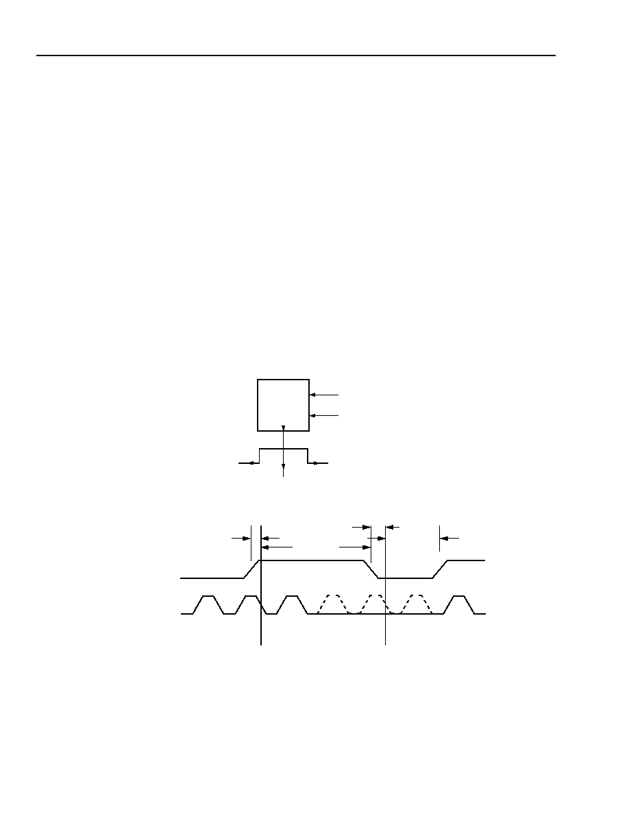
56
56
Lucent Technologies Inc.
Data Sheet
June 1999
ORCA Series 3C and 3T FPGAs
Special Function Blocks
(continued)
Start-Up Logic
The start-up logic block is located in the lower right cor-
ner of the FPGA. This block can be configured to coor-
dinate the relative timing of the release of GSRN, the
activation of all user I/Os, and the assertion of the
DONE signal at the end of configuration. If a start-up
clock is used to time these events, the start-up clock
can come from CCLK, or it can be routed into the start-
up block using lower right corner routing resources.
These signals are described in the Start-Up subsection
of the FPGA States of Operation section.
Clock Control (CLKCNTRL) and StopCLK
There is one CLKCNTRL block in the MID section of
the interquad routing on each side of the FPGA. This
block is used to selectively distribute the fast clock to
the PLC array and the left (top) and right (bottom)
ExpressCLKs (ECKL and ECKR) to the side of the
array on which the CLKCNTRL block resides.
The source clock for the CLKCNTRL block comes
either from the ExpressCLK pad at the middle of the
side of the FPGA or from the corner ExpressCLK route
that comes from the corner ExpressCLK pad (at the
lower left or upper right of the device, whichever is
closer). The programmable clock manager ExpressCLK
output can also be sourced to this corner routing for
distribution at the two closest CLKCNTRL blocks.
Each CLKCNTRL block also features an invertible
StopCLK
shutoff input that is available from local rout-
ing. This feature may be used to glitchlessly stop and
start the clock at the three outputs of each CLKCNTRL
block and has the option of doing so on either the rising
or falling edge of the clock. When the clock is halted
based on its rising edge, it stops and stays at V
DD
.
When it is stopped based on its falling edge, it stops
and stays at GND. If the StopCLK shutoff signal meets
the CLKCNTRL setup and hold times, the clock is
stopped on the second clock cycle after the shutoff sig-
nal. A diagram of the bottom CLKCNTRL block and
StopCLK
timing is shown in Figure 35.
5-5981(F)
Notes:
CLKCNTRL output clocks are ExpressCLK left and right and fast clock.
Clock shutoff shown active-high acting on clock falling edge.
Figure 35. Top CLKCNTRL Function Block
CORNER EXPRESSCLK
CLOCK SHUTOFF
EXPRESSCLK RIGHT
EXPRESSCLK LEFT
FAST CLOCK
CLOCK SHUTOFF
OFF_SET
OFF_HLD
OFF_SET
OFF_HLD
CLKCNTRL OUTPUT
CLOCKS
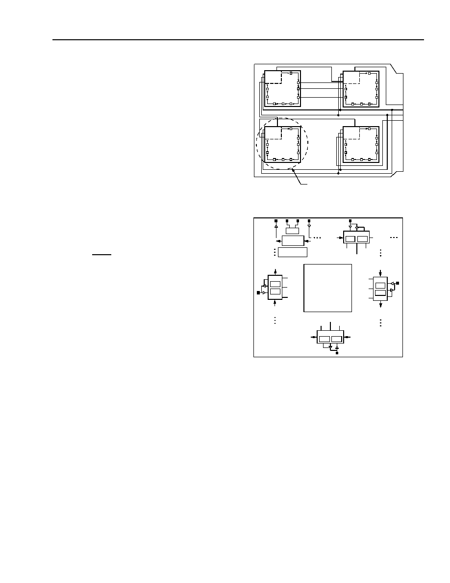
Lucent Technologies Inc.
57
Data Sheet
June 1999
ORCA Series 3C and 3T FPGAs
Special Function Blocks
(continued)
Boundary Scan
The increasing complexity of integrated circuits (ICs)
and IC packages has increased the difficulty of testing
printed-circuit boards (PCBs). To address this testing
problem, the
IEEE
standard 1149.1/D1 (
IEEE
Standard
Test Access Port and Boundary-Scan Architecture) is
implemented in the
ORCA
series of FPGAs. It allows
users to efficiently test the interconnection between
integrated circuits on a PCB as well as test the inte-
grated circuit itself. The
IEEE
1149.1/D1 standard is a
well-defined protocol that ensures interoperability
among boundary-scan (BSCAN) equipped devices
from different vendors.
The
IEEE
1149.1/D1 standard defines a test access
port (TAP) that consists of a four-pin interface with an
optional reset pin for boundary-scan testing of inte-
grated circuits in a system. The
ORCA
Series FPGA
provides four interface pins: test data in (TDI), test
mode select (TMS), test clock (TCK), and test data out
(TDO). The
PRGM
pin used to reconfigure the device
also resets the boundary-scan logic.
The user test host serially loads test commands and
test data into the FPGA through these pins to drive out-
puts and examine inputs. In the configuration shown in
Figure 36, where boundary scan is used to test ICs,
test data is transmitted serially into TDI of the first
BSCAN device (U1), through TDO/TDI connections
between BSCAN devices (U2 and U3), and out TDO of
the last BSCAN device (U4). In this configuration, the
TMS and TCK signals are routed to all boundary-scan
ICs in parallel so that all boundary-scan components
operate in the same state. In other configurations, mul-
tiple scan paths are used instead of a single ring. When
multiple scan paths are used, each ring is indepen-
dently controlled by its own TMS and TCK signals.
Figure 37 provides a system interface for components
used in the boundary-scan testing of PCBs. The three
major components shown are the test host, boundary-
scan support circuit, and the devices under test
(DUTs). The DUTs shown here are
ORCA
Series
FPGAs with dedicated boundary-scan circuitry. The
test host is normally one of the following: automatic test
equipment (ATE), a workstation, a PC, or a micropro-
cessor.
5-5972(F)
Key: BSC = boundary-scan cell, BDC = bidirectional data cell,
and DCC = data control cell.
Figure 36. Printed-Circuit Board with Boundary-
Scan Circuitry
TDI
TMS
TCK
TDO
TDI
TDO
TMS
TCK
U2
net a
net b
net c
PLC
ARRAY
BDC
BSC
p_in
p_ts
SCAN
OUT
SCAN
IN
PR[ij]
DCC
p_out
BDC
BSC
p_in
p_out
p_ts
PL[ij]
DCC
SCAN
IN
SCAN
OUT
BDC
DCC
BSC
p_in
p_out
p_ts
SCAN
OUT
PB[ij]
SCAN
IN
TDO TCK TMS TDI
TAPC
BYPASS
REGISTER
INSTRUCTION
REGISTER
BDC
DCC
BSC
p_in
p_out
p_ts
SCAN
OUT
SCAN
IN
PT[ij]
SEE ENLARGED VIEW BELOW
s
TDI
TDO
TMS
TCK
U3
TDI
TDO
TMS
TCK
U4
TDI
TDO
TMS
TCK
U2
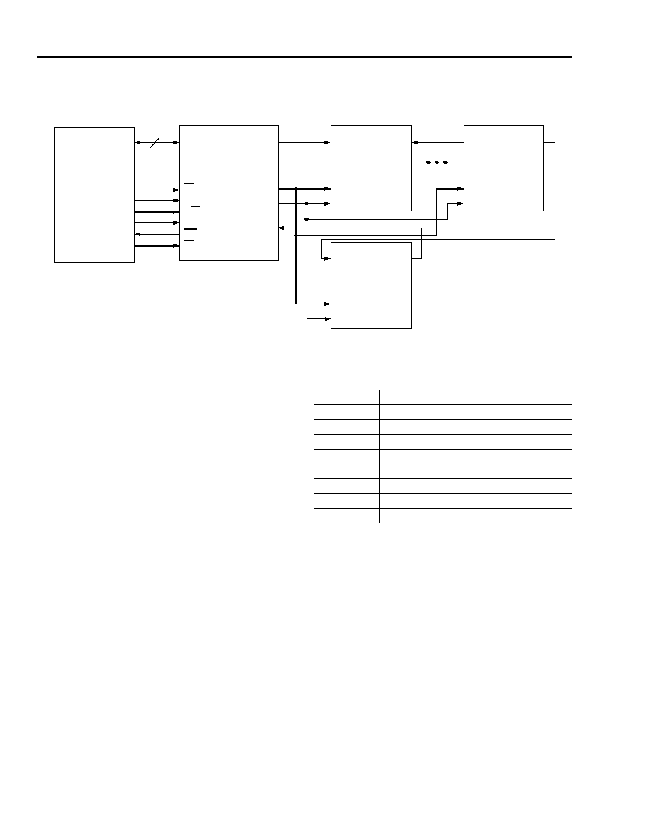
58
Lucent Technologies Inc.
Data Sheet
June 1999
ORCA Series 3C and 3T FPGAs
Special Function Blocks
(continued)
5-6765(F)
Figure 37. Boundary-Scan Interface
D[7:0]
INTR
MICRO-
PROCESSOR
D[7:0]
CE
RA
R/W
DAV
INT
SP
TMS0
TCK
TDI
TDO
TDI
TMS
TCK
TDO
ORCA
SERIES
FPGA
TDI
ORCA
SERIES
FPGA
TMS
TCK
TDO
TDI
TMS
TCK
TDO
ORCA
SERIES
FPGA
LUCENT
BOUNDARY-
SCAN
MASTER
(BSM)
(DUT)
(DUT)
(DUT)
The boundary-scan support circuit shown in Figure 37
is the 497AA Boundary-Scan Master (BSM). The BSM
off-loads tasks from the test host to increase test
throughput. To interface between the test host and the
DUTs, the BSM has a general microprocessor interface
and provides parallel-to-serial/serial-to-parallel conver-
sion, as well as three 8K data buffers. The BSM also
increases test throughput with a dedicated automatic
test-pattern generator and with compression of the test
response with a signature analysis register. The PC-
based boundary-scan test card/software allows a user
to quickly prototype a boundary-scan test setup.
Boundary-Scan Instructions
The
ORCA
Series boundary-scan circuitry is used for
three mandatory
IEEE
1149.1/D1 tests (EXTEST,
SAMPLE/PRELOAD, BYPASS), the optional
IEEE
1149.1/D1 IDCODE instruction, and five
ORCA
-defined
instructions. The 3-bit wide instruction register sup-
ports the nine instructions listed in Table 13, where the
use of PSR1 or USERCODE is selectable by a bit
stream option.
Table 13. Boundary-Scan Instructions
Code
Instruction
000
EXTEST
001
PLC Scan Ring 1 (PSR1)/USERCODE
010
RAM Write (RAM_W)
011
IDCODE
100
SAMPLE/PRELOAD
101
PLC Scan Ring 2 (PSR2)
110
RAM Read (RAM_R)
111
BYPASS

Lucent Technologies Inc.
59
Data Sheet
June 1999
ORCA Series 3C and 3T FPGAs
Special Function Blocks
(continued)
The external test (EXTEST) instruction allows the inter-
connections between ICs in a system to be tested for
opens and stuck-at faults. If an EXTEST instruction is
performed for the system shown in Figure 36, the con-
nections between U1 and U2 (shown by nets a, b, and
c) can be tested by driving a value onto the given nets
from one device and then determining whether the
same value is seen at the other device. This is deter-
mined by shifting 2 bits of data for each pin (one for the
output value and one for the 3-state value) through the
BSR until each one aligns to the appropriate pin. Then,
based upon the value of the 3-state signal, either the
I/O pad is driven to the value given in the BSR, or the
BSR is updated with the input value from the I/O pad,
which allows it to be shifted out TDO.
The SAMPLE/PRELOAD instruction is useful for sys-
tem debugging and fault diagnosis by allowing the data
at the FPGA's I/Os to be observed during normal
operation or written during test operation. The data for
all of the I/Os is captured simultaneously into the BSR,
allowing them to be shifted-out TDO to the test host.
Since each I/O buffer in the PICs is bidirectional, two
pieces of data are captured for each I/O pad: the value
at the I/O pad and the value of the 3-state control sig-
nal. For preload operation, data is written from the BSR
to all of the I/Os simultaneously.
There are five
ORCA
-defined instructions. The PLC
scan rings 1 and 2 (PSR1, PSR2) allow user-defined
internal scan paths using the PLC latches/FFs. The
RAM_Write Enable (RAM_W) instruction allows the
user to serially configure the FPGA through TDI. The
RAM_Read Enable (RAM_R) allows the user to read
back RAM contents on TDO after configuration. The
IDCODE instruction allows the user to capture a 32-bit
identification code that is unique to each device and
serially output it at TDO. The IDCODE format is shown
in Table 14.
Table 14. Boundary-Scan ID Code
* PLC array size of FPGA, reverse bit order.
Note: Table assumes version 0.
Device
Version
(4 bits)
Part*
(10 bits)
Family
(6 bits)
Manufacturer
(11 bits)
LSB
(1 bit)
OR3T20
0000
0011000000 110000
00000011101
1
OR3T30
0000
0111000000 110000
00000011101
1
OR3C/T55
0000
0100100000 110000
00000011101
1
OR3C/T80
0000
0110100000 110000
00000011101
1
OR3T125
0000
0011100000 110000
00000011101
1
OR3T165
0000
0000010000 110000
00000011101
1
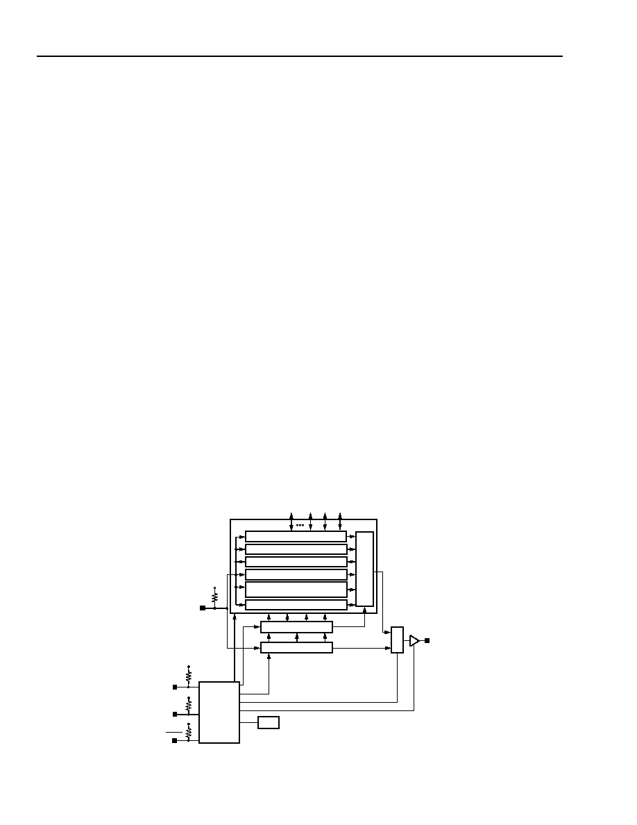
60
60
Lucent Technologies Inc.
Data Sheet
June 1999
ORCA Series 3C and 3T FPGAs
Special Function Blocks
(continued)
ORCA
Boundary-Scan Circuitry
The
ORCA
Series boundary-scan circuitry includes a
test access port controller (TAPC), instruction register
(IR), boundary-scan register (BSR), and bypass regis-
ter. It also includes circuitry to support the four pre-
defined instructions.
Figure 38 shows a functional diagram of the boundary-
scan circuitry that is implemented in the
ORCA
Series.
The input pins' (TMS, TCK, and TDI) locations vary
depending on the part, and the output pin is the dedi-
cated TDO/RD_DATA output pad. Test data in (TDI) is
the serial input data. Test mode select (TMS) controls
the boundary-scan test access port controller (TAPC).
Test clock (TCK) is the test clock on the board.
The BSR is a series connection of boundary-scan cells
(BSCs) around the periphery of the IC. Each I/O pad on
the FPGA, except for CCLK, DONE, and the boundary-
scan pins (TCK, TDI, TMS, and TDO), is included in
the BSR. The first BSC in the BSR (connected to TDI)
is located in the first PIC I/O pad on the left of the top
side of the FPGA (PTA PIC). The BSR proceeds clock-
wise around the top, right, bottom, and left sides of the
array. The last BSC in the BSR (connected to TDO) is
located on the top of the left side of the array (PL1D).
The bypass instruction uses a single FF, which resyn-
chronizes test data that is not part of the current scan
operation. In a bypass instruction, test data received on
TDI is shifted out of the bypass register to TDO. Since
the BSR (which requires a two FF delay for each pad)
is bypassed, test throughput is increased when devices
that are not part of a test operation are bypassed.
The boundary-scan logic is enabled before and during
configuration. After configuration, a configuration
option determines whether or not boundary-scan logic
is used.
The 32-bit boundary-scan identification register con-
tains the manufacturer's ID number, unique part num-
ber, and version (as described earlier). The
identification register is the default source for data on
TDO after RESET if the TAP controller selects the shift-
data-register (SHIFT-DR) instruction. If boundary scan
is not used, TMS, TDI, and TCK become user I/Os,
and TDO is 3-stated or used in the readback operation.
An optional USERCODE is available if the boundary-
scan PSR1 instruction is not used. The selection
between PSR1 and USERCODE is a configuration
option and can be performed in
ORCA
Foundry. The
USERCODE is an 11-bit value that the user can set
during device configuration and can be written to and
read from the FPGA via the boundary-scan logic. The
USERCODE value replaces the manufacturer field of
the boundary-scan ID code when the USERCODE
instruction is issued, allowing users to have configured
devices identified in a user-defined manner. The manu-
facturer ID field remains available when the IDCODE
instruction is issued.
5-5768(F)
Figure 38.
ORCA
Series Boundary-Scan Circuitry Functional Diagram
TAP
CONTROLLER
TMS
TCK
BOUNDARY-SCAN REGISTER
PSR2 REGISTER (PLCs)
BYPASS REGISTER
DATA
MUX
INSTRUCTION DECODER
INSTRUCTION REGISTER
M
U
X
RESET
CLOCK IR
SHIFT-IR
UPDATE-IR
PUR
TDO
SELECT
ENABLE
RESET
CLOCK DR
SHIFT-DR
UPDATE-DR
TDI
DATA REGISTERS
PSR1 REGISTER (PLCs)
CONFIGURATION REGISTER
(RAM_R, RAM_W)
PRGM
I/O BUFFERS
V
DD
V
DD
V
DD
V
DD
IDCODE REGISTER
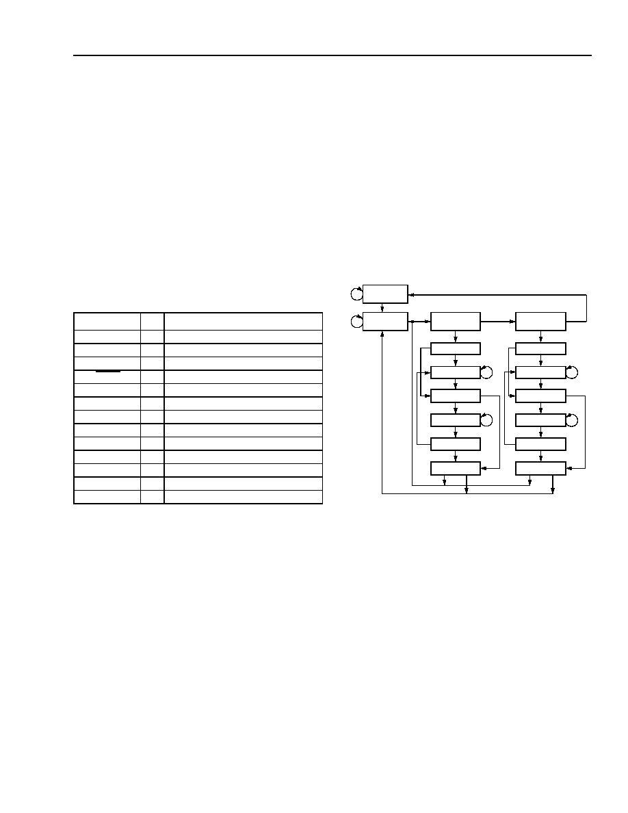
Lucent Technologies Inc.
61
Data Sheet
June 1999
ORCA Series 3C and 3T FPGAs
Special Function Blocks
(continued)
ORCA
Series TAP Controller (TAPC)
The
ORCA
Series TAP controller (TAPC) is a 1149.1/
D1 compatible test access port controller. The 16 JTAG
state assignments from the
IEEE
1149.1/D1 specifica-
tion are used. The TAPC is controlled by TCK and
TMS. The TAPC states are used for loading the IR to
allow three basic functions in testing: providing test
stimuli (Update-DR), test execution (Run-Test/Idle),
and obtaining test responses (Capture-DR). The TAPC
allows the test host to shift in and out both instructions
and test data/results. The inputs and outputs of the
TAPC are provided in the table below. The outputs are
primarily the control signals to the instruction register
and the data register.
Table 15. TAP Controller Input/Outputs
The TAPC generates control signals that allow capture,
shift, and update operations on the instruction and data
registers. In the capture operation, data is loaded into
the register. In the shift operation, the captured data is
shifted out while new data is shifted in. In the update
operation, either the instruction register is loaded for
instruction decode, or the boundary-scan register is
updated for control of outputs.
The test host generates a test by providing input into
the
ORCA
Series TMS input synchronous with TCK.
This sequences the TAPC through states in order to
perform the desired function on the instruction register
or a data register. Figure 39 provides a diagram of the
state transitions for the TAPC. The next state is deter-
mined by the TMS input value.
5-5370(F)
Figure 39. TAP Controller State Transition Diagram
Symbol
I/O
Function
TMS
I
Test Mode Select
TCK
I
Test Clock
PUR
I
Powerup Reset
PRGM
I
BSCAN Reset
TRESET
O
Test Logic Reset
Select
O
Select IR (High); Select-DR (Low)
Enable
O
Test Data Out Enable
Capture-DR
O
Capture/Parallel Load-DR
Capture-IR
O
Capture/Parallel Load-IR
Shift-DR
O
Shift Data Register
Shift-IR
O
Shift Instruction Register
Update-DR
O
Update/Parallel Load-DR
Update-IR
O
Update/Parallel Load-IR
SELECT-
DR-SCAN
CAPTURE-DR
SHIFT-DR
EXIT1-DR
PAUSE-DR
EXIT2-DR
UPDATE-DR
1
1
0
0
1
0
RUN-TEST/
IDLE
1
TEST-LOGIC-
RESET
SELECT-
IR-SCAN
CAPTURE-IR
SHIFT-IR
EXIT1-IR
PAUSE-IR
EXIT2-IR
UPDATE-IR
1
1
0
1
0
0
0
0
0
1
0
1
1
1
0
1
1
0
0
0
0
1
1
1
0
62
62
Lucent Technologies Inc.
Data Sheet
June 1999
ORCA Series 3C and 3T FPGAs
Special Function Blocks
(continued)
Boundary-Scan Cells
Figure 40 is a diagram of the boundary-scan cell (BSC)
in the
ORCA
series PICs. There are four BSCs in each
PIC: one for each pad, except as noted above. The
BSCs are connected serially to form the BSR. The
BSC controls the functionality of the in, out, and 3-state
signals for each pad.
The BSC allows the I/O to function in either the normal
or test mode. Normal mode is defined as when an out-
put buffer receives input from the PLC array and pro-
vides output at the pad or when an input buffer
provides input from the pad to the PLC array. In the test
mode, the BSC executes a boundary-scan operation,
such as shifting in scan data from an upstream BSC in
the BSR, providing test stimuli to the pad, capturing
test data at the pad, etc.
The primary functions of the BSC are shifting scan data
serially in the BSR and observing input (p_in), output
(p_out), and 3-state (p_ts) signals at the pads. The
BSC consists of two circuits: the bidirectional data cell
is used to access the input and output data, and the
direction control cell is used to access the 3-state
value. Both cells consist of a flip-flop used to shift scan
data which feeds a flip-flop to control the I/O buffer. The
bidirectional data cell is connected serially to the direc-
tion control cell to form a boundary-scan shift register.
The TAPC signals (capture, update, shiftn, treset, and
TCK) and the MODE signal control the operation of the
BSC. The bidirectional data cell is also controlled by
the high out/low in (HOLI) signal generated by the
direction control cell. When HOLI is low, the bidirec-
tional data cell receives input buffer data into the BSC.
When HOLI is high, the BSC is loaded with functional
data from the PLC.
The MODE signal is generated from the decode of the
instruction register. When the MODE signal is high
(EXTEST), the scan data is propagated to the output
buffer. When the MODE signal is low (BYPASS or
SAMPLE), functional data from the FPGA's internal
logic is propagated to the output buffer.
The boundary-scan description language (BSDL) is
provided for each device in the
ORCA
Series of FPGAs
on the
ORCA
Foundry CD. The BSDL is generated
from a device profile, pinout, and other boundary-scan
information.
5-2844(F
Figure 40. Boundary-Scan Cell
D
Q
D
Q
D
Q
D
Q
SCAN IN
p_out
HOLI
BIDIRECTIONAL DATA CELL
I/O BUFFER
DIRECTION CONTROL CELL
MODE
UPDATE/TCK
SCAN OUT
TCK
SHIFTN/CAPTURE
p_ts
p_in
PAD_IN
PAD_TS
PAD_OUT
0
1
0
1
0
1
0
1
0
1
Lucent Technologies Inc.
63
Data Sheet
June 1999
ORCA Series 3C and 3T FPGAs
Special Function Blocks
(continued)
Boundary-Scan Timing
To ensure race-free operation, data changes on specific clock edges. The TMS and TDI inputs are clocked in on
the rising edge of TCK, while changes on TDO occur on the falling edge of TCK. In the execution of an EXTEST
instruction, parallel data is output from the BSR to the FPGA pads on the falling edge of TCK. The maximum fre-
quency allowed for TCK is 10 MHz.
Figure 41 shows timing waveforms for an instruction scan operation. The diagram shows the use of TMS to
sequence the TAPC through states. The test host (or BSM) changes data on the falling edge of TCK, and it is
clocked into the DUT on the rising edge.
5-5971(F)
Figure 41. Instruction Register Scan Timing Diagram
TCK
TMS
TDI
RUN-
T
E
ST/
I
DLE
RU
N-TEST/I
DLE
EX
IT
1-
I
R
EX
IT
2-
I
R
UP
DATE
-I
R
S
E
LE
CT-DR-S
C
AN
CA
PTURE
-I
R
S
E
LE
CT-I
R-
SCA
N
T
E
ST
-LO
G
I
C-R
ESE
T
SHI
FT-
I
R
P
A
US
E-I
R
SHI
FT-
I
R
EX
IT
1-
I
R
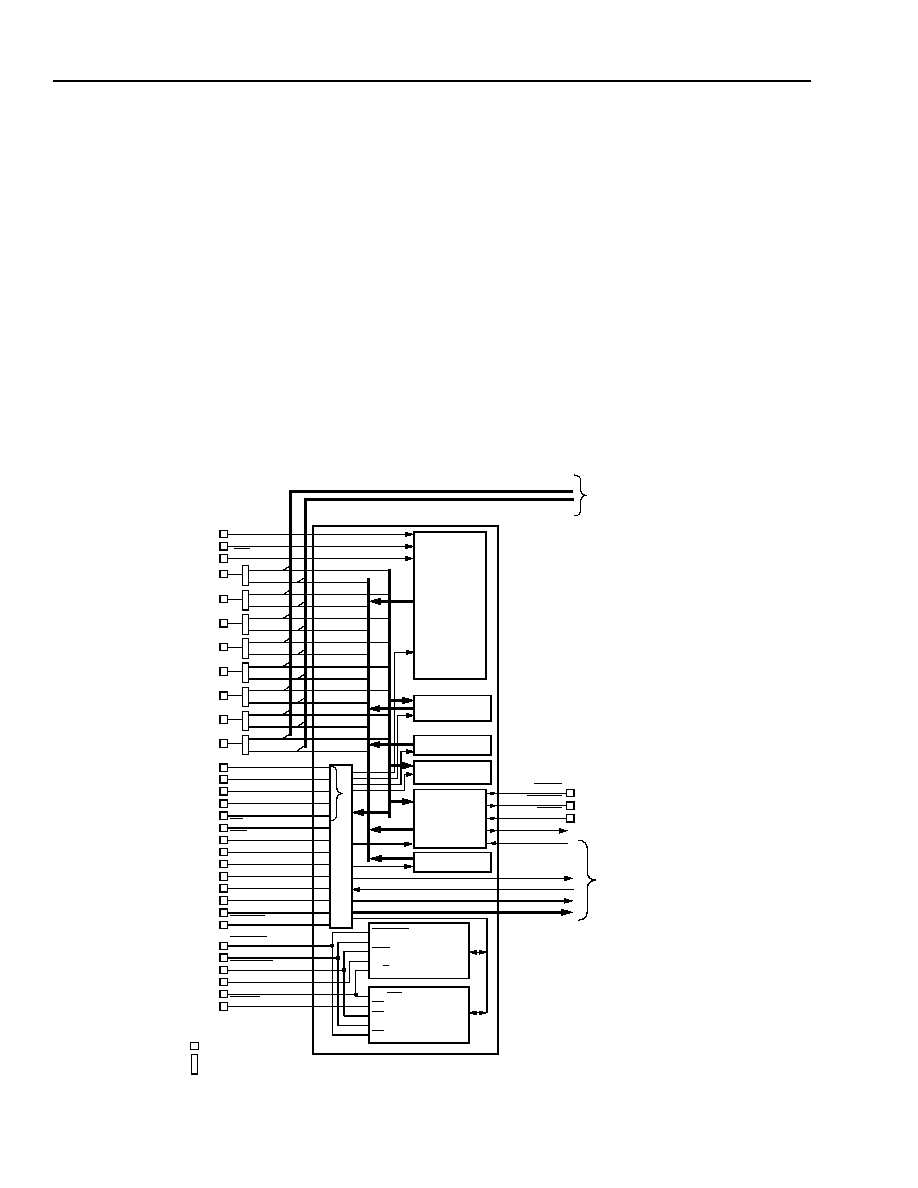
64
64
Lucent Technologies Inc.
Data Sheet
June 1999
ORCA Series 3C and 3T FPGAs
Microprocessor Interface (MPI)
The Series 3 FPGAs have a dedicated synchronous
microprocessor interface function block (see
Figure 42). The MPI is programmable to operate with
PowerPC
MPC800 series microprocessors and
Intel
*
i960
* J core processors; see Table 16 and Table 17,
respectively, for compatible processors. The MPI imple-
ments an 8-bit interface to the host processor (
Pow-
erPC
or
i960
) that can be used for configuration and
readback of the FPGA as well as for user-defined data
processing and general monitoring of FPGA function.
In addition to dedicated-function registers, the micro-
processor interface allows for the control of up to 16
user registers (RAM or flip-flops) in the FPGA logic. A
synchronous/asynchronous handshake procedure is
used to control transactions with user logic in the FPGA
array. There is also capability for the FPGA logic to
interrupt the host processor either by a hard interrupt or
by having the host processor poll the microprocessor
interface.
The control portion of the microprocessor interface is
available following powerup of the FPGA if the mode
pins specify MPI mode, even if the FPGA is not yet con-
figured. The mode pin (M[2:0]) settings can be found in
the FPGA Configuration Modes section of this data
sheet, and the setup and use of the MPI for configura-
tion is discussed in the MPI Setup and Control subsec-
tion. For postconfiguration use, the MPI must be
included in the configuration bit stream by using an MPI
library element in your design from the
ORCA
macro
library, or by setting the MP_USER bit of the MPI con-
figuration control register prior to the start of configura-
tion (MPI registers are discussed later).
*
Intel
and
i960
are registered trademarks of Intel Corporation.
5-5806(F)
Figure 42. MPI Block Diagram
DONE
RD_DATA
INIT
D7
D7IN
D7OUT
D6
D6IN
D6OUT
D5
D5IN
D5OUT
D4
D4IN
D4OUT
D3
D3IN
D3OUT
D2
D2IN
D2OUT
D1
D1IN
D1OUT
D0
D0IN
D0OUT
ORCA 3C/Txxx MPI
STATUS
REGISTER
SCRATCHPAD
REGISTER
READBACK
DATA REGISTER
READBACK
ADDR REGISTER
CONTROL
REGISTERS
PART ID
REGISTERS
RESET
RD_CFG
PRGM
GSR
IRQ
TO GSR BLOCK
TO FPGA
ROUTING
USER_START
USER_END
WR_CTRL
A[3:0]
RDYRCV
CLK
ADS
ALE
W/R
i960 LOGIC
RD/WR
BT
TS
CLKOUT
TA
POWERPC LOGIC
DE
CODE
/
C
ONT
R
OL
PO
W
E
R
P
C
ONL
Y
A4
A3
A2
A1
A0
RD
CS0
CS1
CCLK
M3
M2
M1
M0
MPI_IRQ
MPI_ACK
MPI_CLK
MPI_STRB
MPI_ALE
MPI_RW
MPI_B1
TO FPGA
ROUTING
D[7:0]IN
D[7:0]OUT
DEVICE PAD
I/O BUFFER
Lucent Technologies Inc.
65
Data Sheet
June 1999
ORCA Series 3C and 3T FPGAs
Microprocessor Interface (MPI)
(continued)
PowerPC System
In Figure 43, the
ORCA
FPGA is a memory-mapped
peripheral to the
PowerPC
processor. The
PowerPC
interface uses separate address and data buses and
has several control lines. The
ORCA
chip select lines,
CS0
and CS1, are each connected to an address line
coming from the
PowerPC
. In this manner, the FPGA is
capable of a transaction with the
PowerPC
whenever
the address line connected to
CS0
is low, the address
line for CS1 is high, and there is a valid address on
PowerPC
address lines A[27:31]. Other forms of selec-
tion are possible by using the FPGA chip selects in a
different way. For example,
PowerPC
address bits
A[0:26] could be decoded to select
CS0
and CS1, or if
the FPGA is the only peripheral to the
PowerPC
, CS0
and CS1 could be tied low and high, respectively, to
cause them to always be selected. If the MPI is not
used for FPGA configuration, decoding logic can be
implemented internal or external to the FPGA. If logic
internal to the FPGA is used, the chip selects must be
routed out on an output pin and then connected exter-
nally to
CS0
and/or CS1. If the MPI is to be used for
configuration, any decode logic used must be imple-
mented external to the FPGA since the FPGA logic has
not been configured yet.
5-5761(F)
Note: FPGA shown as a memory-mapped peripheral using
CS0
and
CS1. Other decoding schemes are possible using
CS0
and/or
CS1.
Figure 43.
PowerPC
/MPI
The basic flow of a transaction on the
PowerPC
/MPI
interface is given below. Pin descriptions are shown in
Table 16 and timing is shown in the Timing Characteris-
tics section of this data sheet. For both read and write
transactions, the address, chip select, and read/write
(read high, write low) signals are set up at the FPGA
pins by the
PowerPC
. The
PowerPC
then asserts its
transfer start signal (
TS
) low. Data is available to the
MPI
during a write at the rising clock edge after the
clock cycle during which
TS
is low. The transfer is
acknowledged to the
PowerPC
by the low asser tion of
the
TA
signal. The MPI
PowerPC
interface does not
support burst transfers, so the burst inhibit signal,
BI
, is
also asserted low during the transfer acknowledge . The
same process applies to a read from the MPI except
that the read data is expected at the FPGA data pins by
the
PowerPC
at the rising edge of the clock when
TA
is
low. The MPI only drives
TA
low for one clock cycle.
Interrupt requests can be sent to the
PowerPC
asyn-
chronously to the read/write process. Interrupt requests
are sourced by the user-logic in the FPGA. The MPI will
assert the request to the
PowerPC
as a direct interrupt
signal and/or a pollable bit in the MPI status register
(discussed in the MPI Setup and Control section). The
MPI
will continue to assert the interrupt request until
the user-logic deasserts its interrupt request signal.
Table 16.
PowerPC
/MPI Configuration
DOUT
CCLK
D[7:0]
A[4:0]
MPI_CLK
MPI_RW
MPI_ACK
MPI_BI
MPI_IRQ
MPI_STRB
CS0
CS1
HDC
LDC
D[7:0]
A[27:31]
CLKOUT
RD/WR
TA
BI
IRQx
TS
A26
A25
TO DAISY-
CHAINED
DEVICES
POWERPC
ORCA
8
FPGA
SERIES 3
DONE
INIT
PowerPC
Signal
ORCA Pin
Name
MPI
I/O
Function
D[0:7]
D[7:0]
I/O
8-bit data bus
A[27:31]
A[4:0]
I
5-bit
MPI
address
bus
TS
RD/MPI_STRB
I
Transfer start signal
--
CS0
I
Active-low
MPI
select
--
CS1
I
Active-high
MPI
select
CLKOUT
A7/MPI_CLK
I
PowerPC interface
clock
RD/
WR
A8/MPI_RW
I
Read (high)/write
(low) signal
TA
A9/
MPI_ACK
O
Active-low transfer
acknowledge signal
BI
A10/
MPI_BI
O
Active-low burst
transfer inhibit
signal
Any of
IRQ
[7:0]
A11/
MPI_IRQ
O
Active-low interrupt
request signal
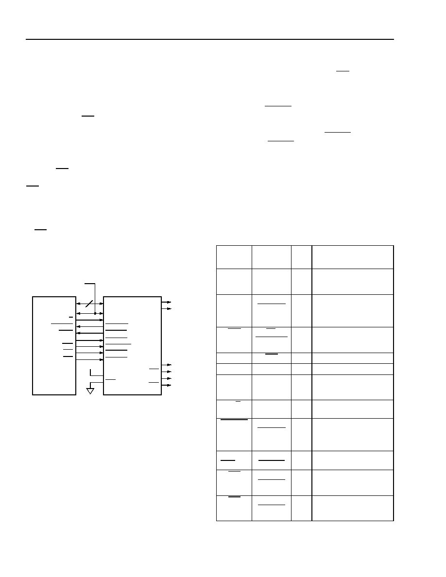
66
66
Lucent Technologies Inc.
Data Sheet
June 1999
ORCA Series 3C and 3T FPGAs
Microprocessor Interface (MPI)
(continued)
i960 System
Figure 44 shows a schematic for connecting the
ORCA
MPI
to supported
i960
processors. In the figure, the
FPGA is shown as the only peripheral, with the FPGA
chip select lines,
CS0
and CS1, tied low and high,
respectively. The
i960
address and data are multi-
plexed onto the same bus. This precludes memory
mapping of the FPGA in the
i960
memory space of a
multiperipheral system without some form of address
latching to capture and hold the address signals to
drive the
CS0
and/or CS1 signals. Multiple address sig-
nals could also be decoded and latched to drive the
CS0
and/or CS1 signals. If the MPI is not used for
FPGA configuration, decoding/latching logic can be
implemented internal or external to the FPGA. If logic
internal to the FPGA is used, the chip selects must be
routed out an output pin and then connected externally
to
CS0
and/or CS1. If the MPI is to be used for configu-
ration, any decode/latch logic used must be imple-
mented external to the FPGA since the FPGA logic has
not been configured yet.
5-5762(F)
Note: FPGA shown as only system peripheral with fixed-chip select
signals. For multiperipheral systems, address decoding and/
or latching can be used to implement chip selects.
Figure 44.
i960
/MPI
The basic flow of a transaction on the
i960
/MPI inter-
face is given below. Pin descriptions are shown in
Table 17, and timing is shown in the
ORCA
Timing
Characteristics section of this data sheet. For both read
and write transactions, the address latch enable (ALE)
is set up by the
i960
at the FPGA to the falling edge of
the clock. The address, byte enables, chip selects, and
read/write (read low, write high) signals are normally
set up at the FPGA pins by the
i960
at the next rising
edge of the clock. At this same rising clock edge, the
i960
asserts its address/data strobe (
ADS
) low. Data is
available to the MPI during a write at the rising clock
edge of the following clock cycle. The transfer is
acknowledged to the
i960
by the low assertion of the
ready/recover (
RDYRCV
) signal. The same process
applies to a read from the MPI except that the read
data is expected at the FPGA data pins by the
i960
at
the rising edge of the clock when
RDYRCV
is low. The
MPI
only drives
RDYRCV
low for one clock cycle.
Interrupts can be sent to the
i960
asynchronously to
the read/write process. Interrupt requests are sourced
by the user-logic in the FPGA. The MPI will assert the
request to the
i960
as a direct interrupt signal and/or a
pollable bit in the MPI status register (discussed in the
MPI
Setup and Control section). The MPI will continue
to assert the interrupt request until the user-logic deas-
serts its interrupt request signal.
Table 17.
i960
/MPI Configuration
DOUT
CCLK
D[7:0]
MPI_CLK
MPI_RW
MPI_ACK
MPI_IRQ
MPI_ALE
MPI_BE1
HDC
LDC
TO DAISY-
CHAINED
DEVICES
ORCA
8
FPGA
SERIES 3
DONE
INIT
AD[7:0]
CLKIN
W/R
RDYRCV
XINTx
ALE
BE1
i960
CS1
CS0
i960 SYSTEM CLOCK
V
DD
MPI_BE0
BE0
MPI_STRB
ADS
i960
Signal
ORCA
Pin
Name
MPI
I/O
Function
AD[7:0]
D[7:0]
I/O
Multiplexed 5-bit address/
8-bit data bus. The
address appears on D[4:0].
ALE
RDY/RCLK/
MPI_ALE
I
Address latch enable used
to capture address from
AD[4:0] on falling edge of
clock.
ADS
RD
/
MPI_STRB
I
Address/data strobe to
indicate start of transac-
tion.
--
CS0
I
Active-low
MPI
select.
--
CS1
I
Active-high
MPI
select.
System
Clock
A7/
MPI_CLK
I
i960 system clock. This
clock is sourced by the
system and not the
i960.
W/
R
A8/MPI_RW
I
Write (high)/read (low)
signal.
RDYRCV
A9/
MPI_ACK
O
Active-low ready/recover
signal indicating acknowl-
edgment of the transac-
tion.
Any of
XINT
[7:0]
A11/
MPI_IRQ
O
Active-low interrupt
request signal.
BE0
A0/
MPI_BE0
I
Byte-enable 0 used as
address bit 0 in
i960 8-bit
mode.
BE1
A1/
MPI_BE1
I
Byte-enable 1 used as
address bit 1 in
i960 8-bit
mode.
Lucent Technologies Inc.
67
Data Sheet
June 1999
ORCA Series 3C and 3T FPGAs
Microprocessor Interface (MPI)
(continued)
MPI Interface to FPGA
The MPI interfaces to the user-programmable FPGA
logic using a 4-bit address, read/write control signal,
interrupt request signal, and user start and user end
handshake signals. Timing numbers are provided so
that the user-logic data transfers can be performed syn-
chronously with the host processor (
PowerPC
or
i960
)
interface clock or asynchronously. Table 18 shows the
internal interface signals between the MPI and the
FPGA user-programmable logic. All of the signals are
connected to the MPI in the upper-left corner of the
device except for the D[7:0] and CLK signals that come
directly from the I/O pin.
The 4-bit addressing from the MPI to the PLCs allows
for up to 16 locations to be addressed by the host pro-
cessor. The user address space of the MPI does not
address any hard register. Rather, the user is free to
construct registers from FFs, latches, or RAM that can
be selected by the addressing. Alternately, the decoded
address signals may be used as control signals for
other functions such as state machines or timers.
The transaction sequence between the MPI and the
user-logic is as follows. When the host processor ini-
tiates a transaction as discussed in the preceding sec-
tions, the MPI outputs the 4-bit user address (UA[3:0])
and the read/write control signal (
URDWR
, which is
read-high, write-low regardless of host processor), and
then asserts the user start signal, USTART. During a
write from the host processor, the user logic can accept
data written by the host processor from the D[7:0] pins
once the USTART signal is asserted. The user logic
ends a transaction by asserting an active-high user
end (UEND) signal to the MPI.
The MPI will insert wait-states in the host processor
bus cycles, holding the host processor until the user-
logic completes its task and returns a UEND signal,
upon which the MPI generates an acknowledge signal.
If the host processor is reading from the FPGA, the
user logic must have the read data available on the
D[7:0] pins of the FPGA when the UEND signal is
asserted. If the user logic is fast or if the MPI user
address is being decoded for use as a control signal,
the MPI transaction time can be minimized by routing
the USTART signal directly to the UEND input of the
MPI
. The timing section of this data sheet contains a
parameter table with delay, setup, and hold timing
requirements to operate the user-logic either synchro-
nously or asynchronously with the MPI host interface
clock.
The user-logic may also assert an active-low interrupt
request (
UIRQ
) to the MPI, which, in turn, asserts an
interrupt to the host processor. Assertion of an inter-
rupt request is asynchronous to the host processor
clock and any read or write transaction occurring in the
MPI
. The user-logic is responsible for providing any
required interrupt vectors for the host processor, and
the user-logic must deassert the interrupt request once
serviced. If the interrupt request is not deasserted in
the user logic, it will continue to be asserted to the host
processor via the MPI_IRQ pin.
Table 18. MPI Internal Interface Signals
Signal
MPI
I/O
Function
UA[3:0]
O
User Logic Address. Addresses up to 16 unique user registers or use as control
signals.
URDWRN
O
User Logic Read/Write Control Signal. High indicates a read from user logic by
the host processor, low indicates a write to user-logic by the host processor.
USTART
O
Active-High User Start Signal. Indicates the start of an MPI transaction between
the host processor and the user logic.
UEND
I
Active-High User End Signal. Indicates that the user-logic is finished with the
current MPI transaction.
UIRQ
I
Active-Low Interrupt. Sends request from the user-logic to the host processor.
D[7:0]
FPGA I/O
User Data. Eight data bits come directly from the FPGA pins--not through the
MPI
.
MPI_CLK
FPGA I
MPI
Clock. The MPI clock is sourced by the host processor and comes directly
from the FPGA pin--not through the MPI.
68
Lucent Technologies Inc.
Data Sheet
June 1999
ORCA Series 3C and 3T FPGAs
Microprocessor Interface (MPI)
(continued)
MPI
Setup and Control
The MPI has a series of addressable registers that provide MPI control and status, configuration and readback data
transfer, FPGA device identification, and a dedicated user scratchpad register. All registers are 8 bits wide. The
address map for these registers and the user-logic address space are shown in Table 19, followed by descriptions
of the register and bit functions. Note that for all registers, the most significant bit is bit 7, and the least significant bit
is bit 0.
Table 19. MPI Setup and Control Registers
Control Register 1
The MPI control register 1 is a read/write register. The host processor writes a control byte to configure the MPI. It
is readable by the host processor to verify the status of control bits previously written.
Table 20. MPI Setup and Control Registers Descriptions
Address
(Hex)
Register
00
Control Register 1.
01
Control Register 2.
02
Scratchpad Register.
03
Status Register.
04
Configuration/Readback Data Register.
05
Readback Address Register 1 (bits [7:0]).
06
Readback Address Register 2 (bits [15:8]).
07
Device ID Register 1 (bits [7:0]).
08
Device ID Register 2 (bits [15:8]).
09
Device ID Register 3 (bits [23:16]).
0A
Device ID Register 4 (bits [31:24]).
0B--0F
Reserved.
10--1F
User-definable Address Space.
Bit #
Description
Bit 0
GSR Input. Setting this bit to a 1 invokes a global set/reset on the FPGA. The host processor must
return this bit to a 0 to remove the GSR signal. GSR does not affect the registers at MPI addresses 0
through F hexadecimal or any configuration registers. Default state = 0.
Bit 1
Reserved.
Bit 2
Reserved.
Bit 3
Reserved.
Bit 4
Reserved.
Bit 5
RD_CFG
Input. Changing this bit to a 0 after configuration will initiate readback. The host processor
must return this bit to a 1 to remove the
RD_CFG
signal. Since this bit works exactly like the
RD_CFG
input pin, please see the FPGA pin descriptions for more information on this signal. Default state = 1.
Bit 6
Reserved.
Bit 7
PRGM
Input. Setting this bit to a 0 causes the FPGA to begin configuration and resets the boundary-
scan circuitry. The host processor must return this bit to a 1 to remove the
PRGM
signal. Since this bit
works exactly like the
PRGM
input pin (except that it does not reset the MPI), please see the FPGA pin
descriptions for more information on this signal. Default state = 1.
Lucent Technologies Inc.
69
Data Sheet
June 1999
ORCA Series 3C and 3T FPGAs
Microprocessor Interface (MPI)
(continued)
Scratchpad Register
The MPI scratchpad register is an 8-bit read/write register with no defined operation. It may be used for any user-
defined function.
Control Register 2
The MPI control register 2 is a read/write register. The host processor writes a control byte to configure the MPI. It
is readable by the host processor to verify the status of control bits it had previously written.
Table 21. MPI Control Register 2
Bit #
Bit Name
Description
Bit 0
EN_IRQ_CFG
Enable
IRQ
for Configuration Data Request in Daisy-Chain Configuration
Mode. Setting this bit to a 1 prior to configuration enables the
IRQ
signal to go active
when new data is requested for configuration writes or is available for configuration
reads to/from the configuration data register. A 0 clears the
IRQ
enable. This bit is
only valid for daisy-chain configuration. Default = 0.
Bit 1
EN_IRQ_ERR
Enable
IRQ
for Bit Stream Error. Setting this bit to a 1 prior to configuration
enables the
IRQ
signal to go active on the occurrence of a bit stream error during
configuration. A 0 clears the
IRQ
enable. This bit only has effect while in configura-
tion mode. Default = 0.
Bit 2
EN_IRQ_USR
Enable
IRQ
from the User FPGA Space. Setting this bit to a 1 allows user-defined
circuitry in the FPGA to generate an interrupt to the host processor by sourcing a
logic low on the
UIRQ
signal in the user logic. Default = 0.
Bit 3
MP_DAISY
MPI
Daisy-Chain Output Enable. Setting this bit to a 1 enables daisy-chain output
of the configuration data. See the Configuration section of this data sheet for daisy-
chain configuration details. Default = 0.
Bit 4
MP_HOLD_BUS Enable Bus Holding During Daisy-Chain Configuration Mode. Setting this bit to
a 1 will cause the MPI to wait until the FPGA configuration logic has serialized a
byte of configuration data before acknowledging the transaction. The data is only
serialized if the MP_DAISY (bit 3 above) control bit is set to 1. If MP_HOLD_BUS is
set to 0, the MPI will immediately acknowledge a configuration data byte transfer.
Immediate acknowledgment allows the host processor to perform other tasks during
FPGA configuration by polling the MPI status register (or by interrupt) and only write
configuration data when the FPGA is ready. Default = 0.
Bit 5
MP_USER
MPI
User Mode Enable. Setting this bit to a 1 will enable the MPI for user mode
operation. MP_USER must be set prior to the FPGA DONE signal going high during
configuration. The MPI may also be enabled for user operation via the configuration
bit stream. Default = 0.
Bit 6
Reserved
--
Bit 7
Reserved
--
70
Lucent Technologies Inc.
Data Sheet
June 1999
ORCA Series 3C and 3T FPGAs
Microprocessor Interface (MPI)
(continued)
Status Register
The microprocessor interface status register is a read-only register, providing information to the host processor.
Table 22. Status Register
Configuration Data Register
The MPI configuration data register is a writable register in configuration mode and a readable register in readback
mode. For FPGA configuration, this is where the configuration data bytes are sequentially written by the host pro-
cessor. Similarly, for readback mode, the MPI provides the readback data bytes in this register for the host proces-
sor.
Readback Address Register 1
The MPI readback address register 1 is a writable register used to accept the least significant address byte
(bits [7:0]) of the configuration data location to be read back.
Readback Address Register 2
The MPI readback address register 2 is a writable register used to accept the most significant address byte
(bits [15:8]) of the configuration data location to be read back.
Bit #
Description
Bit 0
Reserved.
Bit 1
Data Ready. Set by the MPI, a 1 on this bit during configuration alerts the host processor that the FPGA
is ready for another byte of configuration data. During byte-wide readback, the MPI sets this bit to a 1 to
tell the host processor that a byte of configuration data is available for reading. This bit is cleared by a
host processor access (read or write) to the configuration data register.
Bit 2
IRQ
Pending. The MPI sets this bit to 1 to indicate to the host processor that the FPGA has a pending
interrupt request. This bit may be used for the host processor to poll for interrupts if the
MPI_IRQ
pin out-
put of the FPGA has been masked at the host processor. This bit is set to 0 when the status register is
read. Interrupt requests from the FPGA user space must be cleared in FPGA user logic in addition to
reading this bit.
Bits
[4:3]
Bit Stream Error Flags. Bits 3 and 4 are set by the MPI to indicate any error during FPGA configura-
tion. See bit 2 of control register 2 for the capability to alert the host processor of an error via the
IRQ
signal during configuration. In the truth table below, bit 3 is the LSB (bit on right). These bits are cleared
to 0 when
PRGM
goes active:
00 = No error
01 = ID error
10 = Checksum error
11 = Stop-bit/alignment error
Bit 5
Reserved.
Bit 6
INIT.
This bit reflects the binary value of the FPGA
INIT
pin.
Bit 7
DONE. This bit reflects the binary value of the FPGA DONE pin.
Lucent Technologies Inc.
71
Data Sheet
June 1999
ORCA Series 3C and 3T FPGAs
Microprocessor Interface (MPI)
(continued)
Device ID Registers
The MPI device ID is broken into four registers holding 1 byte each. The device ID that is available through the MPI
is the same as the boundary-scan ID code, except that the device ID in the MPI has a reverse bit order. There is no
means to overwrite any of the device ID as can be done with the boundary-scan ID, but the MPI scratchpad register
can be used as a personalization register. The format for the entire device ID is shown below followed by family and
device values and the partitioning of the device ID into the four device ID registers.
Table 23. Device ID Code
* PLC array size of FPGA.
Table 24 shows the family and device values for all parts covered by this data sheet.
Table 24. Series 3 Family and Device ID Values
Table 25 describes the device IDs for all parts covered by this data sheet as they are partitioned into the four regis-
ters found in the MPI.
Table 25.
ORCA
Series 3 Device ID Descriptions
Version
Part*
Family
Manufacturer
MSB
4 bits
10 bits
6 bits
11 bits
1 bit
Example: (First version of Lucent's OR3C55)
0000 0100100000 110000 00000011101 1
Part Name
Family ID
(Hex)
Device ID
(Hex)
OR3T20
03
0C
OR3T30
03
0E
OR3C/T55
03
12
OR3C/T80
03
16
OR3T125
03
1C
Device ID Register 1
Bit 0
Logic 1. This bit is always a one.
Bits [7:1]
0011101, the 7 least significant bits of the Lucent Technologies manufacturer ID.
Device ID Register 2
Bits [3:0]
0000, the 4 most significant bits of the Lucent Technologies manufacturer ID.
Bits [7:4]
The 4 least significant bits of the 10-bit part number.
Device ID Register 3
Bits [5:0]
The 6 most significant bits of the 10-bit part number.
Bits [7:6]
The 2 least significant bits of the device family code.
Device ID Register 4
Bits [3:0]
The 4 most significant bits of the device family code.
Bits [7:4]
The 4-bit device version code.
72
72
Lucent Technologies Inc.
Data Sheet
June 1999
ORCA Series 3C and 3T FPGAs
Programmable Clock Manager (PCM)
The
ORCA
programmable clock manager (PCM) is a
special function block that is used to modify or condi-
tion clock signals for optimum system performance.
Some of the functions that can be performed with the
PCM
are clock skew reduction (both internal and board
level), duty-cycle adjustment, clock delay reduction,
clock phase adjustment, and clock frequency multipli-
cation/division. Due to the different capabilities required
by customer application, each PCM contains both a
PLL (phase-locked loop) and a DLL (delayed-locked
loop) mode. By using PLC logic resources in conjunc-
tion with the PCM, many other functions, such as fre-
quency synthesis, are possible.
There are two PCMs on each Series 3 device, one in
the lower left corner and one in the upper right corner.
Each can drive two different, but interrelated clock net-
works inside the FPGA. Each PCM can take a clock
input from the ExpressCLK pad in its corner or from
general routing resources. There are also two input
sources that provide feedback to the PCM from the
PLC array. One of these is a dedicated corner Express-
CLK
feedback, and the other is from general routing.
Each PCM sources two clock outputs, one to the corner
ExpressCLK
that feeds the CLKCNTRL blocks on the
two sides adjacent to the PCM, and one to the system
clock spine network through general routing. Figure 45
shows a high-level block diagram of the PCM.
Functionality of the PCM is programmed during opera-
tion through a read/write interface internal to the FPGA
array or via the configuration bit stream. The internal
FPGA interface comprises write enable and read
enable signals, a 3-bit address bus, an 8-bit input (to
the PCM) data bus, and an 8-bit output data bus. There
is also a PCM output signal, LOCK, that indicates a sta-
ble output clock state. These signals are used to pro-
gram a series of registers to configure the PCM
functional core for the desired functionality.
Operation of the PCM is divided into two modes, delay-
locked loop (DLL) and phase-locked loop (PLL). Some
operations can be performed by either mode and some
are specific to a particular mode. These will be
described in each individual mode section. In general,
DLL mode is preferable to PLL mode for the same func-
tion because it is less sensitive to input clock noise.
In the discussions that follow, the duty cycle is the per-
cent of the clock period during which the output clock is
high.
5-5828(F)
Figure 45. PCM Block Diagram
USER CONTROL SIGNALS
PCM-FPGA
INTERFACE
PCM CORE
FUNCTIONS
CORNER EXPRESSCLK IN
GENERAL CLOCKIN
FEEDBACK
ExpressCLK
FEEDBACK CLOCK
FROM ROUTING
EXPRESSCLK OUT
SYSTEM CLOCK OUT
(FROM GENERAL ROUTING)
(TO GENERAL ROUTING)

Lucent Technologies Inc.
73
Data Sheet
June 1999
ORCA Series 3C and 3T FPGAs
Programmable Clock Manager (PCM)
(continued)
PCM Registers
The PCM contains eight user-programmable registers used for configuring the PCM's functionality. Table 26 shows
the mapping of the registers and their functions. See Figure 46 for more information on the location of PCM ele-
ments that are discussed in the table. The PCM registers are referenced in the discussions that follow. Detailed
explanations of all register bits are supplied following the functional description of the PCM.
Table 26. PCM Registers
Address
Function
0
Divider 0 Programming. Programmable divider, DIV0, value and DIV0 reset bit. DIV0 can
divide the input clock to the PCM or can be bypassed.
1
Divider 1 Programming. Programmable divider, DIV1, value and DIV1 reset bit. DIV1 can
divide the feedback clock input to the PCM or can be bypassed. Valid only in PLL mode.
2
Divider 2 Programming. Programmable divider, DIV2, value and DIV2 reset bit. DIV2 can
divide the output of the tapped delay line or can be bypassed and is only valid for the
ExpressCLK
output.
3
DLL 2x Duty-Cycle Programming. DLL mode clock doubler (2x) duty-cycle selection.
4
DLL 1x Duty-Cycle Programming. Depending on the settings in other registers, this regis-
ter is for:
a. PLL mode phase/delay selection;
b. DLL mode 1x duty cycle selection; and
c. DLL mode programmable delay.
5
Mode Programming. DLL/PLL mode selection, DLL 1x/2x clock selection, phase detector
feedback selection.
6
Clock Source Status/Output Clock Selection Programming. Input clock selection, feed-
back clock selection, ExpressCLK output source selection, system clock output source selec-
tion.
7
PCM Control Programming. PCM power, reset, and configuration control.
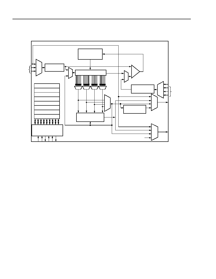
74
Lucent Technologies Inc.
Data Sheet
June 1999
ORCA Series 3C and 3T FPGAs
Programmable Clock Manager (PCM)
(continued)
5-5829(F)
Figure 46. PCM Functional Block Diagram
EXPRESSCLK
FROM
PROGRAMMABLE
DIVIDER
DIV0
REGISTER 7
REGISTER 6
REGISTER 5
REGISTER 4
REGISTER 3
REGISTER 2
REGISTER 1
REGISTER 0
FPGA-PCM INTERFACE
COMBINATORIAL
LOGIC
PROGRAMMABLE
DIVIDER
DIV2
0
1
2
3
S4
0
1
2
3
S10
0
SYSTEM CLOCK
OUTPUT
EXPRESSCLK
OUTPUT
FROM
EXPRESSCLK
FEEDBACK
FEEDBACK
CLOCK
PROGRAMMABLE
DIVIDER
DIV1
0
1
S2
PHASE
DETECTOR
PROGRAMMABLE DELAY
LINES (32 TAPS)
CHARGE PUMP
AND
LOW-PASS FILTER
1
0
S4
1...7
S5
1...7
1...7
1...7
S6
S7
S8
0
1
2
3
S4
0
1
2
3
S3
PCM
INPUT
CLOCK
DAT
A
_
I
N[7
:
0
]
A
D
DR_IN[2
:0]
DA
T
A
_
O
UT
[7
:0
]
WE
RE
LO
C
K
PAD
ROUTING
0
1
2
3
S0
ROUTING

Lucent Technologies Inc.
75
Data Sheet
June 1999
ORCA Series 3C and 3T FPGAs
Programmable Clock Manager (PCM)
(continued)
Delay-Locked Loop (DLL) Mode
DLL mode is used for implementing a delayed clock
(phase adjustment), clock doubling, and duty cycle
adjustment. All DLL functions stem from a delay line
with 32 taps. The delayed input clock is pulled from var-
ious taps and processed to implement the desired
result. There is no feedback clock in DLL mode, provid-
ing a very stable output and a fast lock time for the out-
put clock.
DLL mode is selected by setting bit 0 in PCM register
five to a 0. The settings for the various submodes of
DLL mode are described in the following paragraphs.
Divider DIV0 may be used with any of the DLL modes
to divide the input clock by an integer factor of 1 to 8
prior to implementation of the DLL process.
Delayed Clock
A delayed version of the input clock can be constructed
in DLL mode. The output clock can be delayed by
increments of 1/32 of the input clock period. Express
CLK and system CLK outputs in delay modes are
selected by setting register six, bits [5:4] to 10 or 11 for
ExpressCLK
output, and/or bits [7:6] to 10 for system
clock output. The delay value is entered in register four.
See register four programming details for more infor-
mation. Delay values are also shown in the second col-
umn of Table 27.
Note that when register six, bits [5:4] are set to 11, the
ExpressCLK
output is divided by an integer factor from
1 to 8 while the system clock cannot be divided. The
ExpressCLK
divider is provided so that the I/O clocking
provided by the ExpressCLK can operate slower than
the internal system clock. This allows for very fast inter-
nal processing while maintaining slower interface
speeds off-chip for improved noise and power perfor-
mance or to interoperate with slower devices in the sys-
tem. The divisor of the ExpressCLK frequency is
selected in register two. See the register two program-
ming details for more information.
1x Clock Duty-Cycle Adjustment
A duty-cycle adjusted replica of the input clock can be
constructed in DLL mode. The duty cycle can be
adjusted in 1/32 (3.125%) increments of the input clock
period. DLL 1x clock mode is selected by setting bit 4
of register five to a 1, and output clock source selection
is selected by setting register six, bits [5:4] to 01 for
ExpressCLK
output, and/or bits [7:6] to 01 for system
clock output. The duty-cycle percentage value is
entered in register four. See register four programming
details for more information. Duty cycle values are also
shown in the third column of Table 27.
Table 27. DLL Mode Delay/1x Duty Cycle
Programming Values
Register 4 [7:0]
7 6 5 4 3 2 1 0
Delay
(CLK_IN/32)
Duty Cycle
(% of CLK_IN)
0 0 X X X 0 0 0
1
3.125
0 0 X X X 0 0 1
2
6.250
0 0 X X X 0 1 0
3
9.375
0 0 X X X 0 1 1
4
12.500
0 0 X X X 1 0 0
5
15.625
0 0 X X X 1 0 1
6
18.750
0 0 X X X 1 1 0
7
21.875
0 0 X X X 1 1 1
8
25.000
0 1 X X X 0 0 0
9
28.125
0 1 X X X 0 0 1
10
31.250
0 1 X X X 0 1 0
11
34.375
0 1 X X X 0 1 1
12
37.500
0 1 X X X 1 0 0
13
40.625
0 1 X X X 1 0 1
14
43.750
0 1 X X X 1 1 0
15
46.875
0 1 1 1 1 X X X
16
50.000
1 0 0 0 0 X X X
17
53.125
1 0 0 0 1 X X X
18
56.250
1 0 0 1 0 X X X
19
59.375
1 0 0 1 1 X X X
20
62.500
1 0 1 0 0 X X X
21
65.625
1 0 1 0 1 X X X
22
68.750
1 0 1 1 0 X X X
23
71.875
1 0 1 1 1 X X X
24
75.000
1 1 0 0 0 X X X
25
78.125
1 1 0 0 1 X X X
26
81.250
1 1 0 1 0 X X X
27
84.375
1 1 0 1 1 X X X
28
87.500
1 1 1 0 0 X X X
29
90.625
1 1 1 0 1 X X X
30
93.750
1 1 1 1 0 X X X
31
96.875
76
76
Lucent Technologies Inc.
Data Sheet
June 1999
ORCA Series 3C and 3T FPGAs
Programmable Clock Manager (PCM)
(continued)
2x Clock Duty-Cycle Adjustment
A doubled-frequency, duty-cycle adjusted version of the
input clock can be constructed in DLL mode. The first
clock cycle of the 2x clock output occurs when the input
clock is high, and the second cycle occurs when the
input clock is low. The duty cycle can be adjusted in
1/32 (6.25%) increments of the input clock period.
Additionally, each of the two doubled-clock cycles that
occurs in a single input clock cycle may be adjusted to
have different duty cycles. DLL 2x clock mode is
selected by setting bit 4 of register five to a 1, and by
setting register six, bits [5:4] to 01 for ExpressCLK out-
put, and/or bits [7:6] to 01 for system clock output. The
duty-cycle percentage value is entered in register
three. See register three programming details for more
information. Duty-cycle values where both cycles of the
doubled clock have the same duty cycle are also shown
in Table 28.
Table 28. DLL Mode Delay/2x Duty Cycle
Programming Values
Phase-Locked Loop (PLL) Mode
The PLL mode of the PCM is used for clock multiplica-
tion (1/8x to 64x) and clock delay minimization func-
tions. PLL functions make use of the PCM dividers and
use feedback signals, often from the FPGA array. The
use of feedback is discussed with each PLL submode.
PLL mode is selected by setting bit 0 of register five to
1.
Clock Delay Minimization
PLL mode can be used to minimize the effects of the
input buffer and input routing delay on the clock signal.
PLL mode causes a feedback clock signal to align in
phase with the input clock (refer back to the block dia-
gram in Figure 45) so that the delay between them is
effectively eliminated.
There is a dedicated feedback path from an adjacent
middle CLKCNTRL block to the PCM. Using the corner
ExpressCLK
pad as the input to the PCM and using this
dedicated feedback path, the clock from the Express-
CLK
output of the PCM, as viewed at the CLKCNTRL
block, will be phase-aligned with the ExpressCLK input
to the PCM. These relationships are diagrammed in
Figure 47.
A feedback clock can also be input to the PCM from
general routing. This allows for compensating for delay
between the PCM input and a point in the general rout-
ing. The use of this routed-feedback path is not gener-
ally recommended. Because compensation is based
on the programmable routing, the amount of clock
delay compensation can vary between FPGA lots and
fabrication processes, and will vary each time that the
feedback line is routed using different resources. Con-
tact Lucent Technologies for application notes regard-
ing the use of routed-feedback delay compensation.
5-5980(F)
Figure 47. ExpressCLK Delay Minimization
Using the PCM
Register 3 [7:0]
7 6 5 4 3 2 1 0
Duty Cycle
(%)
0 0 0 0 0 0 0 0
6.25
0 0 0 0 1 0 0 1
12.50
0 0 0 1 0 0 1 0
18.75
0 0 0 1 1 0 1 1
25.00
0 0 1 0 0 1 0 0
31.25
0 0 1 0 1 1 0 1
37.50
0 0 1 1 0 1 1 0
43.75
0 0 1 1 1 1 1 1
50.00
1 1 0 0 0 0 0 0
56.25
1 1 0 0 1 0 0 1
62.50
1 1 0 1 0 0 1 0
68.75
1 1 0 1 1 0 1 1
75.00
1 1 1 0 0 1 0 0
81.25
1 1 1 0 1 1 0 1
87.50
1 1 1 1 0 1 1 0
93.75
CORNER
CLKCNTRL
CLKCNTRL
DELAY
DELAY IS COMPENSATED
INPUT
OUTPUT WITHOUT
USING PCM
OUTPUT
EXPRESSCLK
EXPRESSCLK
USING PCM
EXPRESSCLK
COMPENSATION EQUALS DELAY

Lucent Technologies Inc.
77
Data Sheet
June 1999
ORCA Series 3C and 3T FPGAs
Programmable Clock Manager (PCM)
(continued)
Clock Multiplication
An output clock that is a multiple (not necessarily an
integer multiple) of the input clock can be generated in
PLL mode. The multiplication ratio is programmed in
the division registers DIV0, DIV1, and DIV2. Note that
DIV2 applies only to the ExpressCLK output of the
PCM
and any reference to DIV2 is implicitly 1 for the
system clock output of the PCM. The clock multiplica-
tion formulas when using ExpressCLK feedback are:
Where the values of DIV0, DIV1, and DIV2 range from
1 to 8.
The ExpressCLK multiplication range of output clock
frequencies is, therefore, from 1/8x up to 8x, with the
system clock range up to 8x the ExpressCLK frequency
or 64x the input clock frequency. If system clock feed-
back is used, the formulas are:
The divider values, DIV0, DIV1, and DIV2 are pro-
grammed in registers zero, one, and two, respectively.
The multiplied output is selected by setting register six,
bits [5:4] to 10 or 11 for ExpressCLK output and/or bits
[7:6] to 10 for system clock output. Note that when reg-
ister six, bits [5:4] are set to 11, the ExpressCLK output
is divided by DIV2, while the system clock cannot be
divided. The ExpressCLK divider is provided so that the
I/O clocking provided by the ExpressCLK can operate
slower than the internal system clock. This allows for
very fast internal processing while maintaining slower
interface speeds off-chip for improved noise and power
performance or to interoperate with slower devices in
the system.
It is also necessary to configure the internal PCM oscil-
lator for operation in the proper frequency range.
Table 29 and Table 30 show the settings required for
register four for a given frequency range for Series 3C
and 3T devices. In addition, the acquisition time is
shown for each frequency range. This is the time that is
required for the PCM to acquire LOCK. The PCM oscil-
lator frequency range is chosen based on the desired
output frequency at the system clock output. If using
the ExpressCLK output, the equivalent system clock
frequency can be selected by multiplying the expected
ExpressCLK
output frequency by the value for DIV2.
Choose the nominal frequency from the table that is
closest to the desired frequency, and use that value to
program register four. Minor adjustments to match the
exact input frequency are then performed automatically
by the PCM.
F
ExpressCLK_OUT
= F
INPUT_CLOCK
∑
DIV1
DIV0
F
SYSTEM_CLOCK_OUT
= F
ExpressCLK_OUT
∑
DIV2
F
SYSTEM_CLOCK_OUT
= F
INPUT_CLOCK
∑
DIV1
DIV0
F
ExpressCLK_OUT
= F
SYSTEM_CLOCK
/
DIV2

78
78
Lucent Technologies Inc.
Data Sheet
June 1999
ORCA Series 3C and 3T FPGAs
Programmable Clock Manager (PCM)
(continued)
Table 29. PCM Oscillator Frequency Range 3Txxx
Note: Use of settings in the first three rows is not recommended.
X means don't care.
Table 30. PCM Oscillator Frequency Range 3Cxx
Note: Use of settings in the first three rows is not recommended.
X means don't care.
Register 4
76543210
Min
(MHz)
System
Clock
Output
Frequency
(MHz)
NOM
Max
(MHz)
T
Acquisition
(µs)
00XXX010
17.00
58.50
100.00
36.00
00XXX011
16.10
52.50
89.00
37.00
00XXX100
15.17
49.00
82.80
38.00
00XXX101
14.25
45.00
76.50
39.00
00XXX110
13.33
41.50
70.30
40.00
00XXX111
12.40
38.00
64.00
41.00
01XXX000
12.20
36.75
61.30
43.75
01XXX001
12.10
35.00
58.00
46.50
01XXX010
11.90
33.00
54.30
49.25
01XXX011
11.70
31.30
51.00
52.00
01XXX100
11.10
30.00
49.40
54.75
01XXX101
10.50
29.15
47.80
57.50
01XXX110
10.00
28.10
46.20
60.25
01XXX111
9.40
27.00
44.60
63.00
10000XXX
9.20
26.25
43.30
65.40
10001XXX
9.00
25.65
42.30
67.80
10010XXX
8.80
25.00
41.30
70.10
10011XXX
8.60
24.45
40.30
72.50
10100XXX
8.40
23.70
39.00
74.90
10101XXX
8.10
22.90
37.70
77.30
10110XXX
7.90
22.20
36.50
79.60
10111XXX
7.70
21.50
35.20
82.00
11000XXX
7.60
20.80
34.00
84.30
11001XXX
7.45
20.10
32.80
86.50
11010XXX
7.30
19.45
31.60
88.80
11011XXX
7.20
18.85
30.50
91.00
11100XXX
6.60
18.30
30.00
93.30
11101XXX
6.00
17.70
29.40
95.50
11110XXX
5.50
17.10
28.60
97.80
11111XXX
5.00
16.50
28.00
100.00
Register 4
76543210
Min
(MHz)
System
Clock
Output
Frequency
(MHz)
NOM
Max
(MHz)
T
Acquisition
(µs)
00XXX010 10.50
73.00
135.00
36.00
00XXX011 10.00
68.00
126.00
37.00
00XXX100
9.50
63.00
117.00
38.00
00XXX101
9.10
58.50
108.00
39.00
00XXX110
8.60
53.80
99.00
40.00
00XXX111
8.10
49.00
90.00
41.00
01XXX000
7.80
47.70
87.50
43.80
01XXX001
7.60
46.30
85.00
46.50
01XXX010
7.30
45.00
82.50
49.30
01XXX011
7.10
43.60
80.00
52.00
01XXX100
6.80
42.10
77.50
55.00
01XXX101
6.50
40.75
75.00
57.50
01XXX110
6.30
39.40
72.50
60.30
01XXX111
6.00
38.00
70.00
63.00
10000XXX
5.90
37.40
68.80
65.40
10001XXX
5.90
36.70
67.50
67.80
10010XXX
5.80
36.00
66.30
70.10
10011XXX
5.80
35.40
65.00
72.50
10100XXX
5.70
35.00
63.80
74.90
10101XXX
5.60
34.10
62.50
77.30
10110XXX
5.60
33.50
61.30
79.60
10111XXX
5.50
32.80
60.00
82.00
11000XXX
5.40
32.10
58.80
84.30
11001XXX
5.40
31.50
57.50
86.50
11010XXX
5.30
30.70
56.30
88.80
11011XXX
5.30
30.10
55.00
91.00
11100XXX
5.20
29.50
53.80
93.30
11101XXX
5.10
28.80
52.50
95.50
11110XXX
5.10
28.20
51.30
97.80
11111XXX
5.00
27.50
50.00
100.00

Lucent Technologies Inc.
79
Data Sheet
June 1999
ORCA Series 3C and 3T FPGAs
Programmable Clock Manager (PCM)
(continued)
PCM/FPGA Internal Interface
Writing and reading the PCM registers is done through
a simple asynchronous interface that connects with the
FPGA routing resources. Reads from the PCM by the
FPGA logic are accomplished by setting up the 3-bit
address, A[2:0], and then applying an active-high read
enable (RE) pulse. The read data will be available as
long as RE is held high. The address may be changed
while RE is high, to read other addresses. When RE
goes low, the data output bus is 3-stated.
Writes to the PCM by the FPGA logic are performed by
applying the write data to the data input bus of the
PCM
, applying the 3-bit address to write to, and assert-
ing the write enable (WE) signal high. Data will be writ-
ten by the high-going transition of the WE pulse.
The read enable (RE) and write enable (WE) signals
may not be active at the same time. For detailed timing
information and specifications, see the Timing Charac-
teristics section of this data sheet.
The LOCK signal output from the PCM to the FPGA
routing indicates a stable output clock signal from the
PCM
. The LOCK signal is high when the PCM output
clock parameters fall within the programmed values
and the PCM specifications for jitter. Due to phase cor-
rections that occur internal to the PCM, the LOCK sig-
nal might occasionally pulse low when the output clock
is out of specification for only one or two clock cycles
(high jitter due to temperature, voltage fluctuation, etc.)
To accommodate these pulses, it is suggested that the
user integrate the LOCK signal over a period suitable to
their application to achieve the desired usage of the
LOCK signal.
The LOCK signal will also pulse high and low during
the acquisition time as the output clock stabilizes. True
LOCK is only achieved when the LOCK signal is a solid
high. Again, it is suggested that the user integrate the
LOCK signal over a time period suitable to the subject
application.
PCM Operation
Several features are available for the control of the
PCM
's overall operation. The PCM may be programma-
bly enabled/disabled via bit 0 of register 7. When dis-
abled, the analog power supply of the PCM is turned
off, conserving power and eliminating the possibility of
inducing noise into the system power buses. Individual
bits (register 7, bits [2:1]) are provided to reset the DLL
and PLL functions of the PCM. These resets affect only
the logic generating the DLL or PLL function; they do
not reset the divider values (DIV0, DIV1, DIV2) or reg-
isters [7:0]. The global set/reset (GSRN) is also pro-
grammably controlled via register 7, bit 7. If register 7,
bit 7 is set to 1, GSRN will have no effect on the PCM
logic, allowing the clock to operate during a global
set/reset. This function allows the FPGA to be reset
without affecting a clock that is sent off-chip and used
elsewhere in the system. Bit 6 of register 7 affects the
functionality of the PCM during configuration. If set to 1,
this bit enables the PCM to operate during configura-
tion, after the PCM has been configured. The PCM
functionality is programmed via the bit stream. If regis-
ter 7, bit 6 is 0, the PCM cannot function and its power
supply is disabled until after the configuration DONE
signal goes high.
When the PCM is powered up via register 7, bit 0, there
is a wake-up time associated with its operation. Follow-
ing the wake-up time, the PCM will begin to fully func-
tion, and, following an acquisition time during which the
output clock may be unstable, the PCM will be in
steady-state operation. There is also a shutdown time
associated with powering off the PCM. The output
clock will be unstable during this period. Waveforms
and timing parameters can be found in the Timing
Characteristics section of this data sheet.

80
Lucent Technologies Inc.
Data Sheet
June 1999
ORCA Series 3C and 3T FPGAs
Programmable Clock Manager (PCM)
(continued)
PCM Detailed Programming
Descriptions of bit fields and individual control bits in the PCM control registers are provided in Table 31. Refer to
Figure 46 for more information on the location of the PCM elements that are discussed. In the following discussion,
the duty cycle is in the percentage of the clock period where the clock is high.
Table 31
.
PCM Control Registers
Bit #
Function
Register 0--Divider 0 Programming
Bits [3:0]
4-Bit Divider, DIV0, Value. This value enables the input clock to immediately be divided by a
value from 1 to 8. A 0 value (the default) indicates that DIV0 is bypassed (no division). Bypass
incurs less delay than dividing by 1. Hexadecimal values greater than 8 for bits [3:0] yield their
modulo 8 value. For example, if bits [3:0] are 1001 (9 hex), the result is divide by 1 (remainder
9/8 = 1).
Bits [6:4]
Reserved.
Bit 7
DIV 0 Reset Bit. DIV0 may not be reset by GSRN depending on the value of register 7, bit 7.
This bit may be set to 1 to reset DIV0 to its default value. Bit 0 must be set to 0 (the default) to
remove the reset.
Register 1--Divider 1 Programming
Bits [3:0]
4-Bit Divider, DIV1, Value. This value enables the feedback clock to be divided by a value from
1 to 8. A 0 value (the default) indicates that DIV1 is bypassed (no division). Bypass incurs less
delay than dividing by 1. Hexadecimal values greater than 8 for bits [3:0] yield their modulo 8
value. For example, if bits [3:0] are 1001 (9 hex), the result is divide by 1 (remainder 9/8 = 1).
Bits [6:4]
Reserved.
Bit 7
DIV1 Reset Bit. DIV1 may not be reset by GSRN, depending on the value of register 7, bit 7.
This bit may be set to 1 to reset DIV1 to its default value. Bit 0 must be set to 0 (the default) to
remove the reset.
Register 2--Divider 2 Programming
Bits [3:0]
4-Bit Divider, DIV2, Value. This value enables the tapped delay line output clock driven onto
ExpressCLK
to be divided by a value from 1 to 8. A 0 value (the default) indicates that DIV2 is
bypassed (no division). Bypass incurs less delay than dividing by 1. Hexadecimal values greater
than 8 for bits [3:0] yield their modulo 8 value. For example, if bits [3:0] are 1001 (9 hex), the
result is divide by 1 (remainder 9/8 = 1).
Bits [6:4]
Reserved.
Bit 7
DIV2 Reset Bit. DIV2 may not be reset by GSRN, depending on the value of register 7, bit 7.
This bit may be set to 1 to reset DIV2 to its default value. Bit 7 must be set to 0 (the default) to
remove the reset.
Register 3--DLL 2x Duty-Cycle Programming
Bits [2:0]
Duty-cycle selection for the doubled clock period associated with the input clock high. The duty
cycle is (value of bit 6) * 50% + ((value of bits [2:0]) + 1) * 6.25%. See the description for bit 6.
Bits [5:3]
Duty-cycle selection for the doubled clock period associated with the input clock low. The duty
cycle is (value of bit 7) * 50% + ((value of bits [2:0]) + 1) * 6.25%. See the description for bit 7.
Bit 6
Master duty-cycle control for the first clock period of the doubled clock: 0 = less than or equal to
50%, 1 = greater than 50%.
Bit 7
Master duty-cycle control for the second clock period of the doubled clock: 0 = less than or equal
to 50%, 1 = greater than 50%. Example: Both clock periods having a 62.5% duty cycle, bits [7:0]
are 11 001 001.

Lucent Technologies Inc.
81
Data Sheet
June 1999
ORCA Series 3C and 3T FPGAs
Programmable Clock Manager (PCM)
(continued)
Table 31. PCM Control Registers (continued)
Bit #
Function
Register 4--DLL 1x Duty-Cycle Programming
Bits [2:0]
Duty-Cycle/Delay Selection for Duty Cycle/Delays Less Than or Equal to 50%. The duty-
cycle/delay is (value of bits [7:6]) * 25% + ((value of bits [2:0]) + 1) * 3.125%. See the description
for bits [7:6].
Bits [5:3]
Duty-Cycle/Delay Selection for Duty Cycle/Delays Greater Than 50%. The duty-cycle/delay
is (value of bits [7:6]) * 25% + ((value of bits [5:3]) + 1) * 3.125%. See the description for bits [7:6].
Bits [7:6]
Master Duty Cycle Control:
00: duty cycle 3.125% to 25%
01: duty cycle 28.125% to 50%
10: duty cycle 53.125% to 75%
11: duty cycle 78.125% to 96.875%
Example: A 40.625% duty cycle, bits [7:0] are 01 XXX 100, where X is a don't care because the
duty cycle is not greater than 50%.
Example: The PCM output clock should be delayed 96.875% (31/32) of the input clock period.
Bits [7:0] are 11110XXX, which is 78.125% from bits [7:6] and 18.75% from bits [5:3]. Bits [2:0]
are don't care (X) because the delay is greater than 50%.
Register 5--Mode Programming
Bit 0
DLL/PLL Mode Selection Bit. 0 = DLL, 1 = PLL. Default is DLL mode.
Bit 1
Reserved.
Bit 2
PLL Phase Detector Feedback Input Selection Bit. 0 = feedback signal from routing/
ExpressCLK
, 1 = feedback from programmable delay line output. Default is 0. Has no effect in
DLL mode.
Bit 3
Reserved.
Bit 4
1x/2x Clock Selection Bit for DLL Mode. 0 = 1x clock output, 1 = 2x clock output. Default is 1x
clock output. Has no effect in PLL mode.
Bits [7:5]
Reserved.

82
Lucent Technologies Inc.
Data Sheet
June 1999
ORCA Series 3C and 3T FPGAs
Programmable Clock Manager (PCM)
(continued)
Table 31. PCM Control Registers (continued)
Bit #
Function
Bits [5:4]
ExpressCLK
Output Source Selector. Default is 00.
00: PCM input clock, bypass path through PCM
01: DLL output
10: tapped delay line output
11: divided (DIV2) delay line output
Bits [7:6]
System Clock Output Source Selector. Default is 00.
00: PCM input clock, bypass path through PCM
01: DLL output
10: tapped delay line output
11: reserved
Register 7--PCM Control Programming
Bit 0
PCM Analog Power Supply Switch. 1 = power supply on, 0 = power supply off.
Bit 1
PCM Reset. A value of 1 resets all PCM logic for PLL and DLL modes.
Bit 2
DLL Reset. A value of 1 resets the clock generation logic for DLL mode. No dividers or user reg-
isters are affected.
Bits [5:3]
Reserved.
Bit 6
PCM Configuration Operation Enable Bit. 0 = normal configuration operation. During configu-
ration (DONE = 0), the PCM analog power supply will be off, the PCM output data bus is 3-stated,
and the LOCK signal is asserted to logic 0. The PCM will power up when DONE = 1.
1 = PCM operation during configuration. The PCM may be powered up (see bit 0) and begin
operation, or continue operation. The setup of the PCM can be performed via the configuration
bit stream.
Bit 7
PCM GSRN Enable Bit. 0 = normal GSRN operation. 1 = GSRN has no effect on PCM logic, so
clock processing will not be interrupted by a chip reset. Default is 0.
Lucent Technologies Inc.
83
Data Sheet
June 1999
ORCA Series 3C and 3T FPGAs
Programmable Clock Manager (PCM)
(continued)
PCM Applications
The applications discussed below are only a small
sampling of the possible uses for the PCM. Check the
Lucent Technologies
ORCA
FPGA Internet website
(listed at the end of this data sheet) for additional appli-
cation notes.
Clock Phase Adjustment
The PCM may be used to adjust the phase of the input
clock. The result is an output clock which has its active
edge either preceding or following the active edge of
the input clock. Clock phase adjustment is accom-
plished in DLL mode by delaying the clock. This is dis-
cussed in the Delay-Locked Loop (DLL) Mode section.
Examples of using the delayed clock as an early or late
phase-adjusted clock are outlined in the following para-
graphs.
An output clock that precedes the input clock can be
used to compensate for clock delay that is largely due
to excessive loading. The preceding output clock is
really not early relative to the input clock, but is delayed
almost a full cycle. This is shown in Figure 48A. The
amount of delay that is being compensated for, plus
clock setup time and some margin, is the amount less
than one full clock cycle that the output clock is delayed
from the input clock.
In some systems, it is desirable to operate logic from
several clocks that operate at different phases. This
technique is often used in microprocessor-based sys-
tems to transfer and process data synchronously
between functional areas, but without incurring exces-
sive delays. Figure 48B shows an input clock and an
output clock operating 180∞ out of phase. It also shows
a version of the input clock that was shifted approxi-
mately 180∞ using logic gates to create an inverter.
Note that the inverted clock is really shifted more than
180∞ due to the propagation delay of the inverter. The
PCM
output clock does not suffer from this delay. Addi-
tionally, the 180∞ shifted PCM output could be shifted
by some smaller amount to effect an early 180∞ shifted
clock that also accounts for loading effects.
In terms of degrees of phase shift, the phase of a clock
is adjustable in DLL mode with resolution relative to the
delay increment (see Table 27):
Phase Adjustment = (Delay)* 11.25,
Delay
<
16
Phase Adjustment = ((Delay)* 11.25) ≠ 360,
Delay > 16
5-5979(F)
Figure 48. Clock Phase Adjustment Using the PCM
INPUT CLOCK
OUTPUT CLOCK
INPUT CLOCK
PCM OUTPUT CLOCK
INVERTED INPUT CLOCK
A. Generating an Early Clock
B. Multiphase Clock Generation Using the DLL
UNINTENDED PHASE
SHIFT DUE TO
INVERTER DELAY
DLL DELAY
DLL DELAY
CLOCK DELAY AND SETUP
BEING COMPENSATED

84
84
Lucent Technologies Inc.
Data Sheet
June 1999
ORCA Series 3C and 3T FPGAs
Programmable Clock Manager (PCM)
(continued)
High-Speed Internal Processing with Slow I/Os
The PCM PLL mode provides two outputs, one sent to
the global system clock routing of the FPGA and the
other to the ExpressCLK(s) that serve the FPGA I/Os.
The ExpressCLK output of the PCM has a divide capa-
bility (DIV2) that the system clock output does not. This
feature allows an input clock to be multiplied up to a
higher frequency for high-speed internal processing,
and also allows the ExpressCLK output to be divided
down to a lower frequency to accommodate off-FPGA
data transfers. For example, a 10 MHz input clock may
be multiplied (see Clock Multiplication in the Phase-
Locked Loop (PLL) Mode subsection) to 25 MHz (DIV0
= 4, DIV1 = 5, DIV2 = 2) and output to the FPGA
ExpressCLK
. This allows the I/Os of the circuit to run at
25 MHz ((2 * 5)/4 * 10 MHz). The system clock will run
at DIV2 times the ExpressCLK rate, which is 2 times
25 MHz, or 50 MHz. This setup allows for internal pro-
cessing to occur at twice the rate of on/off device I/O
transfers.
PCM Cautions
Cautions do apply when using the PCM. There are a
number of configurations that are possible in the PCM
that are theoretically valid, but may not produce viable
results. This section describes some of those situa-
tions, and should leave the user with an understanding
of the types of pitfalls that must be avoided when modi-
fying clock signals.
Resultant signals from the PCM must meet the FPGA
timing specifications. It is possible to specify pulses by
using duty-cycle adjustments that are too narrow to
function in the FPGA. For instance, if a 40 MHz clock is
doubled to 80 MHz and a 6.25% duty cycle is selected,
the result will be a 780 ps pulse that repeats every
12.5 ns. This pulse falls outside of the clock pulse width
specification and is not valid.
Using divider DIV2, it is possible to specify a clock mul-
tiplication factor of 64 between the input clock and the
output system clock. As mentioned above, the resultant
frequency must meet all FPGA timing specifications.
The input clock must also meet the minimum specifica-
tions. An input clock rate that is below the PCM clock
minimum cannot be used even if the multiplied output is
within the allowable range.
The use of the PCM to tweak a clock signal to eliminate
a particular problem, such as a single setup time viola-
tion, is discouraged. A small shift in delay, duty cycle, or
phase to correct a single-point problem is in essence
an asynchronous patch to a synchronous system, mak-
ing the system less stable. This type of local problem,
as opposed to a global clock control issue like device-
wide clock delay, can usually be eliminated through
more robust design practices. If this type of change is
made, the designer must be aware that depending on
the extent of the change made, the design may fail to
operate correctly in a different speed grade or voltage
grade (e.g., 3C vs. 3T), or even in a different production
lot of the same device.
Divider DIV2 is available in DLL mode for the Express-
CLK
output, but its use is not recommended with duty-
cycle adjusted clocks.
Lucent Technologies Inc.
85
Data Sheet
June 1999
ORCA Series 3C and 3T FPGAs
FPGA States of Operation
Prior to becoming operational, the FPGA goes through
a sequence of states, including initialization, configura-
tion, and start-up. Figure 49 outlines these three FPGA
states.
Figure 49. FPGA States of Operation
Initialization
Upon powerup, the device goes through an initialization
process. First, an internal power-on-reset circuit is trig-
gered when power is applied. When V
DD
reaches the
voltage at which portions of the FPGA begin to operate
(2.5 V to 3 V for the OR3Cxx, 2.2 V to 2.7 V for the
OR3Txxx), the I/Os are configured based on the con-
figuration mode, as determined by the mode select
inputs M[2:0]. A time-out delay is initiated when V
DD
reaches between 3.0 V and 4.0 V (OR3Cxx) or 2.7 V to
3.0 V (OR3Txxx) to allow the power supply voltage to
stabilize. The
INIT
and DONE outputs are low. At pow-
erup, if V
DD
does not rise from 2.0 V to V
DD
in less than
25 ms, the user should delay configuration by inputting
a low into
INIT
,
PRGM
, or
RESET
until V
DD
is greater
than the recommended minimum operating voltage
(4.75 V for OR3Cxx commercial devices and 3.0 V for
OR3Txxx devices).
At the end of initialization, the default configuration
option is that the configuration RAM is written to a low
state. This prevents shorts prior to configuration. As a
configuration option, after the first configuration (i.e., at
reconfiguration), the user can reconfigure without
clearing the internal configuration RAM first. The
active-low, open-drain initialization signal
INIT
is
released and must be pulled high by an external resis-
tor when initialization is complete. To synchronize the
configuration of multiple FPGAs, one or more
INIT
pins
should be wire-ANDed. If
INIT
is held low by one or
more FPGAs or an external device, the FPGA remains
in the initialization state.
INIT
can be used to signal that
the FPGAs are not yet initialized. After
INIT
goes high
for two internal clock cycles, the mode lines (M[3:0])
are sampled, and the FPGA enters the configuration
state.
The high during configuration (HDC), low during config-
uration (
LDC
), and DONE signals are active outputs in
the FPGA's initialization and configuration states. HDC,
LDC
, and DONE can be used to provide control of
external logic signals such as reset, bus enable, or
PROM enable during configuration. For parallel master
configuration modes, these signals provide PROM
enable control and allow the data pins to be shared
with user logic signals.
5-4529(F)
≠ ACTIVE I/O
≠ RELEASE INTERNAL RESET
≠ DONE GOES HIGH
START-UP
INITIALIZATION
CONFIGURATION
RESET
OR
PRGM
LOW
PRGM
LOW
≠ CLEAR CONFIGURATION
≠ INIT LOW, HDC HIGH, LDC LOW
OPERATION
POWERUP
≠ POWER-ON TIME DELAY
≠ M[3:0] MODE IS SELECTED
≠ CONFIGURATION DATA FRAME
≠ INIT HIGH, HDC HIGH, LDC LOW
≠ DOUT ACTIVE
YES
NO
NO
RESET,
INIT,
OR
PRGM
LOW
BIT
ERROR
YES
WRITTEN
MEMORY
86
86
Lucent Technologies Inc.
Data Sheet
June 1999
ORCA Series 3C and 3T FPGAs
FPGA States of Operation
(continued)
If configuration has begun, an assertion of
RESET
or
PRGM
initiates an abort, returning the FPGA to the ini-
tialization state. The
PRGM
and
RESET
pins must be
pulled back high before the FPGA will enter the config-
uration state. During the start-up and operating states,
only the assertion of
PRGM
causes a reconfiguration.
In the master configuration modes, the FPGA is the
source of configuration clock (CCLK). In this mode, the
initialization state is extended to ensure that, in daisy-
chain operation, all daisy-chained slave devices are
ready. Independent of differences in clock rates, master
mode devices remain in the initialization state an addi-
tional six internal clock cycles after
INIT
goes high.
When configuration is initiated, a counter in the FPGA
is set to 0 and begins to count configuration clock
cycles applied to the FPGA. As each configuration data
frame is supplied to the FPGA, it is internally assem-
bled into data words. Each data word is loaded into the
internal configuration memory. The configuration load-
ing process is complete when the internal length count
equals the loaded length count in the length count field,
and the required end of configuration frame is written.
All OR3Cxx I/Os operate as TTL inputs during configu-
ration (OR3Txxx I/Os are CMOS-only). All I/Os that are
not used during the configuration process are
3-stated with internal pull-ups.
Warning: During configuration, all OR3Txxx inputs
have internal pull-ups enabled. If these inputs are
driven to 5V, they will draw substantial current (
5 ma).
This is due to the fact that the inputs are pulled up to
3V.
During configuration, the PIC and PLC latches/FFs are
held set/reset and the internal BIDI buffers are 3-
stated. The combinatorial logic begins to function as
the FPGA is configured. Figure 50 shows the general
waveform of the initialization, configuration, and start-
up states.
Configuration
The
ORCA
Series FPGA functionality is determined by
the state of internal configuration RAM. This configura-
tion RAM can be loaded in a number of different
modes. In these configuration modes, the FPGA can
act as a master or a slave of other devices in the sys-
tem. The decision as to which configuration mode to
use is a system design issue. Configuration is dis-
cussed in detail, including the configuration data format
and the configuration modes used to load the configu-
ration data in the FPGA, following a description of the
start-up state.
5-4482(F)
Figure 50. Initialization/Configuration/Start-Up Waveforms
V
DD
M[3:0]
CCLK
HDC
LDC
DONE
USER I/O
INTERNAL
RESET
(gsrn)
CONFIGURATION
OPERATION
INITIALIZATION
START-UP
RESET
PRGM
INIT

Lucent Technologies Inc.
87
Data Sheet
June 1999
ORCA Series 3C and 3T FPGAs
FPGA States of Operation
(continued)
Start-Up
After configuration, the FPGA enters the start-up
phase. This phase is the transition between the config-
uration and operational states and begins when the
number of CCLKs received after
INIT
goes high is equal
to the value of the length count field in the configuration
frame and when the end of configuration frame has
been written. The system design issue in the start-up
phase is to ensure the user I/Os become active without
inadvertently activating devices in the system or caus-
ing bus contention. A second system design concern is
the timing of the release of global set/reset of the PLC
latches/FFs.
There are configuration options that control the relative
timing of three events: DONE going high, release of the
set/reset of internal FFs, and user I/Os becoming
active. Figure 51 shows the start-up timing for
ORCA
FPGAs. The system designer determines the relative
timing of the I/Os becoming active, DONE going high,
and the release of the set/reset of internal FFs. In the
ORCA
Series FPGA, the three events can occur in any
arbitrary sequence. This means that they can occur
before or after each other, or they can occur simulta-
neously.
There are four main start-up modes: CCLK_NOSYNC,
CCLK_SYNC, UCLK_NOSYNC, and UCLK_SYNC.
The only difference between the modes starting with
CCLK and those starting with UCLK is that for the
UCLK modes, a user clock must be supplied to the
start-up logic. The timing of start-up events is then
based upon this user clock, rather than CCLK. The dif-
ference between the SYNC and NOSYNC modes is
that for SYNC mode, the timing of two of the start-up
events, release of the set/reset of internal FFs, and the
I/Os becoming active is triggered by the rise of the
external DONE pin followed by a variable number of ris-
ing clock edges (either CCLK or UCLK). For the
NOSYNC mode, the timing of these two events is
based only on either CCLK or UCLK.
DONE is an open-drain bidirectional pin that may
include an optional (enabled by default) pull-up resistor
to accommodate wired ANDing. The open-drain DONE
signals from multiple FPGAs can be tied together
(ANDed) with a pull-up (internal or external) and used
as an active-high ready signal, an active-low PROM
enable, or a reset to other portions of the system.
When used in SYNC mode, these ANDed DONE pins
can be used to synchronize the other two start-up
events, since they can all be synchronized to the same
external signal. This signal will not rise until all FPGAs
release their DONE pins, allowing the signal to be
pulled high.
The default for
ORCA
is the CCLK_SYNC synchro-
nized start-up mode where DONE is released on the
first CCLK rising edge, C1 (see Figure 51). Since this is
a synchronized start-up mode, the open-drain DONE
signal can be held low externally to stop the occurrence
of the other two start-up events. Once the DONE pin
has been released and pulled up to a high level, the
other two start-up events can be programmed individu-
ally to either happen immediately or after up to four ris-
ing edges of CCLK (Di, Di + 1, Di + 2, Di + 3, Di + 4).
The default is for both events to happen immediately
after DONE is released and pulled high.
A commonly used design technique is to release
DONE one or more clock cycles before allowing the I/O
to become active. This allows other configuration
devices, such as PROMs, to be disconnected using the
DONE signal so that there is no bus contention when
the I/Os become active. In addition to controlling the
FPGA during start-up, other start-up techniques that
avoid contention include using isolation devices
between the FPGA and other circuits in the system,
reassigning I/O locations, and maintaining I/Os as 3-
stated outputs until contentions are resolved.
Each of these start-up options can be selected during
bit stream generation in
ORCA
Foundry, using
Advanced Options. For more information, please see
the
ORCA
Foundry documentation.
88
88
Lucent Technologies Inc.
Data Sheet
June 1999
ORCA Series 3C and 3T FPGAs
FPGA States of Operation
(continued)
Note: F = finished, no more CLKs required.
5-2761(F)
Figure 51. Start-Up Waveforms
Reconfiguration
To reconfigure the FPGA when the device is operating
in the system, a low pulse is input into
PRGM
. The con-
figuration data in the FPGA is cleared, and the I/Os not
used for configuration are 3-stated. The FPGA then
samples the mode select inputs and begins reconfigu-
ration. When reconfiguration is complete, DONE is
released, allowing it to be pulled high.
Partial Reconfiguration
All
ORCA
device families have been designed to allow
a partial reconfiguration of the FPGA at any time. This
is done by setting a bit stream option in the previous
configuration sequence that tells the FPGA to not reset
all of the configuration RAM during a reconfiguration.
Then only the configuration frames that are to be modi-
fied need to be rewritten, thereby reducing the configu-
ration time.
Other bit stream options are also available that allow
one portion of the FPGA to remain in operation while a
partial reconfiguration is being done. If this is done, the
user must be careful to not cause contention between
the two configurations (the bit stream resident in the
FPGA and the partial reconfiguration bit stream) as the
second reconfiguration bit stream is being loaded.
Other Configuration Options
There are many other configuration options available to
the user that can be set during bit stream generation in
ORCA
Foundry. These include options to enable
boundary scan and/or the microprocessor interface
(MPI) and/or the programmable clock manager (PCM),
readback options, and options to control and use the
internal oscillator after configuration.
Other useful options that affect the next configuration
(not the current configuration process) include options
to disable the global set/reset during configuration, dis-
able the 3-state of I/Os during configuration, and dis-
able the reset of internal RAMs during configuration to
allow for partial configurations (see above). For more
information on how to set these and other configuration
options, please see the
ORCA
Foundry documenta-
tion.
Di
C1
C2
C3
C4
F
C1
C2
C3
C4
C1
C2
C3
C4
C1, C2, C3, OR C4
Di + 1
Di
Di + 2
Di + 3
Di + 4
Di + 1
Di
Di + 2
Di + 3
Di + 4
CCLK_SYNC
DONE IN
U1
U2
U3
U4
F
U1
U2
U3
U4
U1
U2
U3
U4
UCLK_NOSYNC
Di + 1
Di
Di + 2
Di + 3
Di + 4
Di + 1
Di + 2
Di + 3
UCLK_SYNC
UCLK PERIOD
SYNCHRONIZATION UNCERTAINTY
DONE IN
F
C1
C1
U1, U2, U3, OR U4
DONE
I/O
GSRN
ACTIVE
DONE
I/O
GSRN
ACTIVE
DONE
I/O
GSRN
ACTIVE
DONE
I/O
GSRN
ACTIVE
UCLK
F
CCLK_NOSYNC

Lucent Technologies Inc.
89
Data Sheet
June 1999
ORCA Series 3C and 3T FPGAs
Configuration Data Format
The
ORCA
Foundry Development System interfaces
with front-end design entry tools and provides tools to
produce a fully configured FPGA. This section dis-
cusses using the
ORCA
Foundry Development System
to generate configuration RAM data and then provides
the details of the configuration frame format.
The
ORCA
OR3Cxx and OR3Txxx Series FPGAs are
bit stream compatible.
Using
ORCA Foundry
to Generate
Configuration RAM Data
The configuration data bit stream defines the I/O func-
tionality, logic, and interconnections within the FPGA.
The bit stream is generated by the development sys-
tem. The bit stream created by the bit stream genera-
tion tool is a series of 1s and 0s used to write the FPGA
configuration RAM. It can be loaded into the FPGA
using one of the configuration modes discussed later.
In the bit stream generator, the designer selects
options that affect the FPGA's functionality. Using the
output of the bit stream generator, circuit_name.bit,
the development system's download tool can load the
configuration data into the
ORCA
series FPGA evalua-
tion board from a PC or workstation.
Alternatively, a user can program a PROM (such as a
Serial ROM or a standard EPROM) and load the FPGA
from the PROM. The development system's PROM
programming tool produces a file in .mks or .exo for-
mat.
Configuration Data Frame
Configuration data can be presented to the FPGA in
two frame formats: autoincrement and explicit. A
detailed description of the frame formats is shown in
Figure 52, Figure 53, and Table 32. The two modes are
similar except that autoincrement mode uses assumed
address incrementation to reduce the bit stream size,
and explicit mode requires an address for each data
frame. In both cases, the header frame begins with a
series of 1s and a preamble of 0010, followed by a
24-bit length count field representing the total number
of configuration clocks needed to complete the loading
of the FPGAs.
Following the header frame is a mandatory ID frame.
(Note that the ID frame was optional in the
ORCA
2C
and 2C/TxxA Series.)
The ID frame contains data used to determine if the bit
stream is being loaded to the correct type of
ORCA
FPGA (i.e., a bit stream generated for an OR3C55 is
being sent to an OR3C55). Error checking is always
enabled for Series 3 devices, through the use of an
8-bit checksum. One bit in the ID frame also selects
between the autoincrement and explicit address modes
for this load of the configuration data.
A configuration data frame follows the ID frame. A data
frame starts with a 01-start bit pair and ends with
enough 1-stop bits to reach a byte boundary. If using
autoincrement configuration mode, subsequent data
frames can follow. If using explicit mode, one or more
address frames must follow each data frame, telling the
FPGA at what addresses the preceding data frame is
to be stored (each data frame can be sent to multiple
addresses).
Following all data and address frames is the postam-
ble. The format of the postamble is the same as an
address frame with the highest possible address value
with the checksum set to all ones.
90
Lucent Technologies Inc.
Data Sheet
June 1999
ORCA Series 3C and 3T FPGAs
Configuration Data Format
(continued)
5-5759(F)
Figure 52. Serial Configuration Data Format--Autoincrement Mode
5-5760(F)
Figure 53. Serial Configuration Data Format--Explicit Mode
Table 32. Configuration Frame Format and Contents
* In MPI configuration mode, the number of stop bits = 32.
Note: For slave parallel mode, the byte containing the preamble must be 11110010. The number of leading header dummy bits must
be (n
*
8) + 4, where n is any nonnegative integer and the number of trailing dummy bits must be (n
*
8), where n is any positive
integer. The number of stop bits/frame for slave parallel mode must be (x
*
8), where x is a positive integer. Note also that the bit
stream generator tool supplies a bit stream that is compatible with all configuration modes, including slave parallel mode.
Header
11110010
Preamble
24-bit Length Count
Configuration frame length.
11111111
Trailing header--8 bits.
ID Frame
0101 1111 1111 1111
ID frame header.
Configuration Mode
00 = autoincrement, 01 = explicit.
Reserved [41:0]
Reserved bits set to 0.
ID
20-bit part ID.
Checksum
8-bit checksum.
11111111
Eight stop bits (high) to separate frames.
Configuration
Data
Frame
(repeated for each
data frame)
01
Data frame header.
Data Bits
Number of data bits depends upon device.
Alignment Bits = 0
String of 0 bits added to bit stream to make frame header, plus data
bits reach a byte boundary.
Checksum
8-bit checksum.
11111111
Eight stop bits (high) to separate frames.
Configuration
Address
Frame
00
Address frame header.
14 Address Bits
14-bit address of location to start data storage.
Checksum
8-bit checksum.
11111111
Eight stop bits (high) to separate frames.
Postamble
00
Postamble header.
11111111 111111
Dummy address.
1111111111111111
16 stop bits.*
CONFIGURATION DATA
CONFIGURATION DATA
1 0
0 1
0 1
PREAMBLE LENGTH
ID FRAME
CONFIGURATION
CONFIGURATION
POSTAMBLE
CONFIGURATION HEADER
0 0
0 0
COUNT
DATA FRAME 1
DATA FRAME 2
PREAMBLE LENGTH
ID FRAME
CONFIGURATION CONFIGURATION
POSTAMBLE
CONFIGURATION HEADER
ADDRESS
ADDRESS
0 0
COUNT
DATA FRAME 1
DATA FRAME 2
FRAME 2
FRAME 1
CONFIGURATION DATA
CONFIGURATION DATA
1 0
0 1
0 1
0 0
0 0
0 0

Lucent Technologies Inc.
91
Data Sheet
June 1999
ORCA Series 3C and 3T FPGAs
Configuration Data Format
(continued)
The length and number of data frames and information on the PROM size for the Series 3 FPGAs are given in
Table 33.
Table 33. Configuration Frame Size
Bit Stream Error Checking
There are three different types of bit stream error checking performed in the
ORCA
Series 3 FPGAs:
ID frame, frame alignment, and CRC checking.
The ID data frame is sent to a dedicated location in the FPGA. This ID frame contains a unique code for the device
for which it was generated. This device code is compared to the internal code of the FPGA. Any differences are
flagged as an ID error. This frame is automatically created by the bit stream generation program in
ORCA
Foundry.
Each data and address frame in the FPGA begins with a frame start pair of bits and ends with eight stop bits set to
1. If any of the previous stop bits were a 0 when a frame start pair is encountered, it is flagged as a frame align-
ment error.
Error checking is also done on the FPGA for each frame by means of a checksum byte. If an error is found on eval-
uation of the checksum byte, then a checksum/parity error is flagged. The checksum is the XOR of all the data
bytes, from the start of frame up to and including the bytes before the checksum. It applies to the ID, address, and
data frames.
When any of the three possible errors occur, the FPGA is forced into an idle state, forcing INIT low. The FPGA will
remain in this state until either the
RESET
or
PRGM
pins are asserted.
If using either of the MPI modes to configure the FPGA, the specific type of bit stream error is written to one of the
MPI
registers by the FPGA configuration logic. The
PGRM
bit of the MPI control register can also be used to reset
out of the error condition and restart configuration.
Devices
OR3T20
OR3T30
OR3C/T55
OR3C/T80
OR3T125
# of Frames
856
984
1240
1496
1880
Data Bits/Frame
202
232
292
352
442
Configuration Data (# of frames x # of data
bits/frame)
172,912
228,288
362,080
526,592
830,960
Maximum Total # Bits/Frame (align bits, 01
frame start, 8-bit checksum, 8 stop bits)
224
256
312
376
464
Maximum Configuration Data (# bits/frame
x # of frames)
191,744
251,904
386,880
562,496
872,320
Maximum PROM Size (bits)
(add configuration header and postamble)
191,912
252,072
387,048
562,664
872,488
92
92
Lucent Technologies Inc.
Data Sheet
June 1999
ORCA Series 3C and 3T FPGAs
FPGA Configuration Modes
There are eight methods for configuring the FPGA.
Seven of the configuration modes are selected on the
M0, M1, and M2 inputs. The eighth configuration mode
is accessed through the boundary-scan interface. A
fourth input, M3, is used to select the frequency of the
internal oscillator, which is the source for CCLK in
some configuration modes. The nominal frequencies of
the internal oscillator are 1.25 MHz and 10 MHz. The
1.25 MHz frequency is selected when the M3 input is
unconnected or driven to a high state.
There are three basic FPGA configuration modes:
master, slave, and peripheral. The configuration data
can be transmitted to the FPGA serially or in parallel
bytes. As a master, the FPGA provides the control sig-
nals out to strobe data in. As a slave device, a clock is
generated externally and provided into the CCLK input.
In the three peripheral modes, the FPGA acts as a
microprocessor peripheral. Table 34 lists the functions
of the configuration mode pins. Note that two configura-
tion modes previously available on the OR2Cxx and
OR2C/TxxA devices (master parallel down and syn-
chronous peripheral) have been removed for Series 3
devices.
Table 34. Configuration Modes
*
Motorola
is a registered trademark of Motorola, Inc.
Master Parallel Mode
The master parallel configuration mode is generally
used to interface to industry-standard, byte-wide mem-
ory, such as the 2764 and larger EPROMs. Figure 54
provides the connections for master parallel mode. The
FPGA outputs an 18-bit address on A[17:0] to memory
and reads 1 byte of configuration data on the rising
edge of RCLK. The parallel bytes are internally serial-
ized starting with the least significant bit, D0. D[7:0] of
the FPGA can be connected to D[7:0] of the micropro-
cessor only if a standard prom file format is used. If a
.bit or .rbt file is used from
ORCA
Foundry, then the
user must mirror the bytes in the .bit or .rbt file OR
leave the .bit or .rbt file unchanged and connect D[7:0]
of the FPGA to D[0:7] of the microprocessor.
Figure 54. Master Parallel Configuration Schematic
In master parallel mode, the starting memory address
is 00000 Hex, and the FPGA increments the address
for each byte loaded.
One master mode FPGA can interface to the memory
and provide configuration data on DOUT to additional
FPGAs in a daisy-chain. The configuration data on
DOUT is provided synchronously with the falling edge
of CCLK. The frequency of the CCLK output is eight
times that of RCLK.
M2
M1
M0
CCLK
Configuration
Mode
Data
0
0
0
Output
Master Serial
Serial
0
0
1
Input
Slave Parallel
Parallel
0
1
0
Output
Microprocessor:
Motorola
*
Pow-
erPC
Parallel
0
1
1
Output
Microprocessor:
Intel i960
Parallel
1
0
0
Output
Master Parallel
Parallel
1
0
1
Output
Async Peripheral
Parallel
1
1
0
Reserved
1
1
1
Input
Slave Serial
Serial
EPROM
A[17:0]
DONE
M2
M1
M0
HDC
ORCA
SERIES
FPGA
RCLK
LDC
V
DD
D[7:0]
DOUT
CCLK
TO DAISY-
CHAINED
DEVICES
V
DD
OR GND
PRGM
PROGRAM
A[17:0]
D[7:0]
OE
CE
Lucent Technologies Inc.
93
Data Sheet
June 1999
ORCA Series 3C and 3T FPGAs
FPGA Configuration Modes
(continued)
Master Serial Mode
In the master serial mode, the FPGA loads the configu-
ration data from an external serial ROM. The configura-
tion data is either loaded automatically at start-up or on
a
PRGM
command to reconfigure. The ATT1700A
Series Serial PROMs can be used to configure the
FPGA in the master serial mode. This provides a sim-
ple 4-pin interface in a compact package.
Configuration in the master serial mode can be done at
powerup and/or upon a configure command. The sys-
tem or the FPGA must activate the serial ROM's
RESET
/OE and
CE
inputs. At powerup, the FPGA and
serial ROM each contain internal power-on reset cir-
cuitry that allows the FPGA to be configured without
the system providing an external signal. The power-on
reset circuitry causes the serial ROM's internal address
pointer to be reset. After powerup, the FPGA automati-
cally enters its initialization phase.
The serial ROM/FPGA interface used depends on such
factors as the availability of a system reset pulse, avail-
ability of an intelligent host to generate a configure
command, whether a single serial ROM is used or mul-
tiple serial ROMs are cascaded, whether the serial
ROM contains a single or multiple configuration pro-
grams, etc. Because of differing system requirements
and capabilities, a single FPGA/serial ROM interface is
generally not appropriate for all applications.
Data is read in the FPGA sequentially from the serial
ROM. The DATA output from the serial ROM is con-
nected directly into the DIN input of the FPGA. The
CCLK output from the FPGA is connected to the CLK
input of the serial ROM. During the configuration pro-
cess, CCLK clocks one data bit on each rising edge.
Since the data and clock are direct connects, the
FPGA/serial ROM design task is to use the system or
FPGA to enable the
RESET
/OE and
CE
of the serial
ROM(s). There are several methods for enabling the
serial ROM's
RESET
/OE and
CE
inputs. The serial
ROM's
RESET
/OE is programmable to function with
RESET active-high and
OE
active-low or
RESET
active-
low and OE active-high.
In Figure 55, serial ROMs are cascaded to configure
multiple daisy-chained FPGAs. The host generates a
500 ns low pulse into the FPGA's
PRGM
input. The
FPGA's
INIT
input is connected to the serial ROMs'
RESET
/OE input, which has been programmed to
function with
RESET
active-low and OE active-high.
The FPGA DONE is routed to the
CE
pin. The low on
DONE enables the serial ROMs. At the completion of
configuration, the high on the FPGA's DONE disables
the serial ROM.
Serial ROMs can also be cascaded to support the con-
figuration of multiple FPGAs or to load a single FPGA
when configuration data requirements exceed the
capacity of a single serial ROM. After the last bit from
the first serial ROM is read, the serial ROM outputs
CEO
low and 3-states the DATA output. The next serial
ROM recognizes the low on
CE
input and outputs con-
figuration data on the DATA output. After configuration
is complete, the FPGA's DONE output into
CE
disables
the serial ROMs.
This FPGA/serial ROM interface is not used in applica-
tions in which a serial ROM stores multiple configura-
tion programs. In these applications, the next
configuration program to be loaded is stored at the
ROM location that follows the last address for the previ-
ous configuration program. The reason the interface in
Figure 55 will not work in this application is that the low
output on the
INIT
signal would reset the serial ROM
address pointer, causing the first configuration to be
reloaded.
In some applications, there can be contention on the
FPGA's DIN pin. During configuration, DIN receives
configuration data, and after configuration, it is a user
I/O. If there is contention, an early DONE at start-up
(selected in
ORCA
Foundry) may correct the problem.
An alternative is to use
LDC
to drive the serial ROM's
CE
pin. In order to reduce noise, it is generally better to
run the master serial configuration at 1.25 MHz (M3 pin
tied high), rather than 10 MHz, if possible.
Figure 55. Master Serial Configuration Schematic
ATT1700A
DIN
M2
M1
M0
ORCA
SERIES
FPGA
CCLK
DOUT
TO DAISY-
CHAINED
DEVICES
DATA
CLK
CE
CEO
ATT1700A
DATA
CLK
RESET/OE
CEO
CE
TO MORE
SERIAL ROMs
AS NEEDED
DONE
INIT
PROGRAM
RESET/OE
PRGM
5-4456.1(F)
94
94
Lucent Technologies Inc.
Data Sheet
June 1999
ORCA Series 3C and 3T FPGAs
FPGA Configuration Modes
(continued)
Asynchronous Peripheral Mode
Figure 56 shows the connections needed for the asyn-
chronous peripheral mode. In this mode, the FPGA
system interface is similar to that of a microprocessor-
peripheral interface. The microprocessor generates the
control signals to write an 8-bit byte into the FPGA. The
FPGA control inputs include active-low
CS0
and active-
high CS1 chip selects and
WR
and
RD
inputs. The chip
selects can be cycled or maintained at a static level
during the configuration cycle. Each byte of data is writ-
ten into the FPGA's D[7:0] input pins. D[7:0] of the
FPGA can be connected to D[7:0] of the microproces-
sor only if a standard prom file format is used. If a .bit or
.rbt file is used from
ORCA
Foundry, then the user must
mirror the bytes in the .bit or .rbt file OR leave the .bit or
.rbt file unchanged and connect D[7:0] of the FPGA to
D[0:7] of the microprocessor.
The FPGA provides an RDY/
BUSY
status output to indi-
cate that another byte can be loaded. A low on RDY/
BUSY
indicates that the double-buffered hold/shift reg-
isters are not ready to receive data, and this pin must
be monitored to go high before another byte of data
can be written. The shortest time RDY/
BUSY
is low
occurs when a byte is loaded into the hold register and
the shift register is empty, in which case the byte is
immediately transferred to the shift register. The long-
est time for RDY/
BUSY
to remain low occurs when a
byte is loaded into the holding register and the shift
register has just started shifting configuration data into
configuration RAM.
The RDY/
BUSY
status is also available on the D7 pin by
enabling the chip selects, setting
WR
high, and apply-
ing
RD
low, where the
RD
input provides an output
enable for the D7 pin when
RD
is low. The D[6:0] pins
are not enabled to drive when
RD
is low and, therefore,
only act as input pins in asynchronous peripheral
mode. Optionally, the user can ignore the RDY/
BUSY
status and simply wait until the maximum time it would
take for the RDY/
BUSY
line to go high, indicating the
FPGA is ready for more data, before writing the next
data byte.
Figure 56. Asynchronous Peripheral Configuration
Microprocessor Interface
(MPI)
Mode
The built-in MPI in Series 3 FPGAs is designed for use
in configuring the FPGA. Figure 57 and Figure 58 show
the glueless interface for FPGA configuration and read-
back from the
PowerPC
and
i960
processors, respec-
tively. When enabled by the mode pins, the MPI
handles all configuration/readback control and hand-
shaking with the host processor. For single FPGA con-
figuration, the host sets the configuration control
register
PRGM
bit to zero then back to a one and, after
reading that the
INIT
signal is high in the MPI status
register, transfers data 8 bits at a time to the FPGA's
D[7:0] input pins.
If configuring multiple FPGAs through daisy-chain
operation is desired, the MP_DAISY bit must be set in
the configuration control register of the MPI. Because
of the latency involved in a daisy-chain configuration,
the MP_HOLD_BUS bit may be set to zero rather than
one for daisy-chain operation. This allows the MPI to
acknowledge the data transfer before the configuration
information has been serialized and transferred on the
FPGA daisy-chain. The early acknowledgment frees
the host processor to perform other system tasks. Con-
figuring with the MP_HOLD_BUS bit at zero requires
that the host microprocessor poll the RDY/
BUSY
bit of
the MPI status register and/or use the MPI interrupt
capability to confirm the readiness of the MPI for more
configuration data.
MICRO-
PROCESSOR
D[7:0]
CS1
M2
M1
M0
HDC
ORCA
SERIES
FPGA
8
LDC
V
DD
DONE
CS0
DOUT
CCLK
TO DAISY-
CHAINED
DEVICES
BUS
CONTROLLER
ADDRESS
DECODE LOGIC
RD
WR
RDY/BUSY
INIT
PRGM
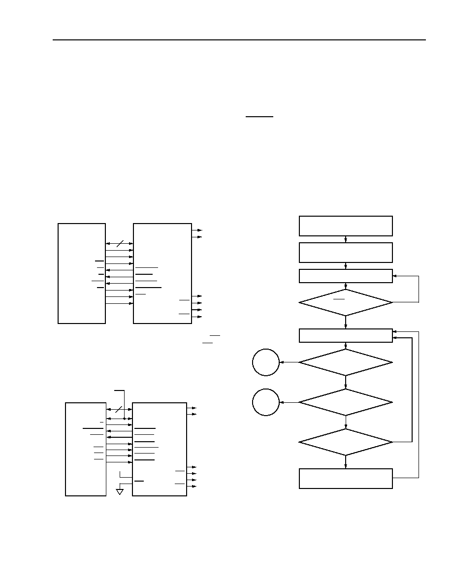
Lucent Technologies Inc.
95
Data Sheet
June 1999
ORCA Series 3C and 3T FPGAs
FPGA Configuration Modes
(continued)
There are two options for using the host interrupt
request in configuration mode. The configuration con-
trol register offers control bits to enable the interrupt on
either a bit stream error or to notify the host processor
when the FPGA is ready for more configuration data.
The MPI status register may be used in conjunction
with, or in place of, the interrupt request options. The
status register contains a 2-bit field to indicate the bit
stream error status. As previously mentioned, there is
also a bit to indicate the MPI's readiness to receive
another byte of configuration data. A flow chart of the
MPI
configuration process is shown in Figure 59. The
MPI
status and configuration register bit maps can be
found in the Special Function Blocks section and MPI
configuration timing information is available in the Tim-
ing Characteristics section of this data sheet.
5-5761(F)
Note: FPGA shown as a memory-mapped peripheral using
CS0
and
CS1. Other decoding schemes are possible using
CS0
and/or
CS1.
Figure 57.
PowerPC
/MPI Configuration Schematic
5-5762(F)
Note: FPGA shown as only system peripheral with fixed chip select
signals. For multiperipheral systems, address decoding and/
or latching can be used to implement chip selects.
Figure 58.
i960
/MPI Configuration Schematic
Configuration readback can also be performed via the
MPI
when it is in user mode. The MPI is enabled in user
mode by setting the MP_USER bit to 1 in the configura-
tion control register prior to the start of configuration or
through a configuration option. To perform readback,
the host processor writes the 14-bit readback start
address to the readback address registers and sets the
RD_CFG
bit to 0 in the configuration control register.
Readback data is returned 8 bits at a time to the read-
back data register and is valid when the DATA_RDY bit
of the status register is 1. There is no error checking
during readback. A flow chart of the MPI readback
operation is shown in Figure 60. The RD_DATA pin
used for dedicated FPGA readback is invalid during
MPI
readback.
5-5763(F)
Figure 59. Configuration Through MPI
DOUT
CCLK
D[7:0]
A[4:0]
MPI_CLK
MPI_RW
MPI_ACK
MPI_BI
MPI_IRQ
MPI_STRB
CS0
CS1
HDC
LDC
D[7:0]
A[27:31]
CLKOUT
RD/WR
TA
BI
IRQx
TS
A26
A25
TO DAISY-
CHAINED
DEVICES
POWERPC
ORCA
8
FPGA
SERIES 3
DONE
INIT
DOUT
CCLK
D[7:0]
MPI_CLK
MPI_RW
MPI_ACK
MPI_IRQ
MPI_ALE
MPI_BE1
HDC
LDC
TO DAISY-
CHAINED
DEVICES
ORCA
8
FPGA
SERIES 3
DONE
INIT
AD[7:0]
CLKIN
W/R
RDYRCV
XINTx
ALE
BE1
i960
CS1
CS0
i960 SYSTEM CLOCK
V
DD
MPI_BE0
BE0
MPI_STRB
ADS
POWER ON WITH
WRITE CONFIGURATION
READ STATUS REGISTER
INIT = 1?
NO
READ STATUS REGISTER
BIT STREAM ERROR?
DATA_RDY = 1?
WRITE DATA TO
DONE = 1?
DONE
ERROR
YES
YES
YES
NO
NO
YES
NO
VALID M[3:0]
CONTROL REGISTER BITS
CONFIGURATION DATA REG
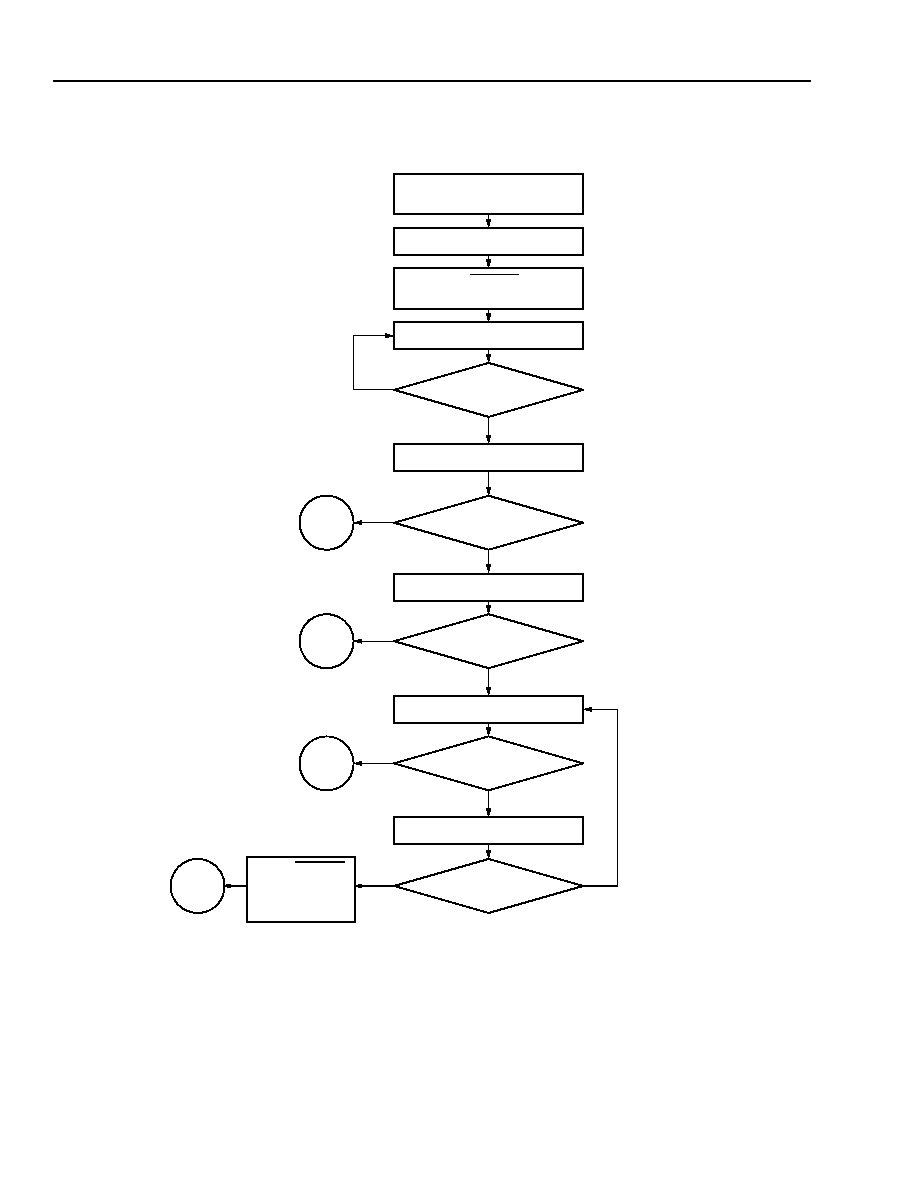
96
Lucent Technologies Inc.
Data Sheet
June 1999
ORCA Series 3C and 3T FPGAs
FPGA Configuration Modes
(continued)
5-5764(F)
Figure 60. Readback Through MPI
ENABLE MICROPROCESSOR
SET READBACK ADDRESS
WRITE RD_CFG TO 0
DATA_RDY = 1?
READ DATA REGISTER
START OF FRAME
DATA = 0xFF?
YES
YES
READ STATUS REGISTER
IN CONTROL REGISTER 1
INTERFACE IN USER MODE
READ DATA REGISTER
FOUND?
READ UNTIL END OF FRAME
FINISHED
READBACK?
YES
YES
WRITE RD_CFG
CONTROL
STOP
NO
NO
ERROR
NO
ERROR
NO
READ DATA REGISTER
DATA = 0xFF?
YES
NO
ERROR
TO 1 IN
REGISTER 1
Lucent Technologies Inc.
97
Data Sheet
June 1999
ORCA Series 3C and 3T FPGAs
FPGA Configuration Modes
(continued)
Slave Serial Mode
The slave serial mode is primarily used when multiple
FPGAs are configured in a daisy-chain (see the Daisy-
Chaining section). It is also used on the FPGA evalua-
tion board that interfaces to the download cable. A
device in the slave serial mode can be used as the lead
device in a daisy-chain. Figure 61 shows the connec-
tions for the slave serial configuration mode.
The configuration data is provided into the FPGA's DIN
input synchronous with the configuration clock CCLK
input. After the FPGA has loaded its configuration data,
it retransmits the incoming configuration data on
DOUT. CCLK is routed into all slave serial mode
devices in parallel.
Multiple slave FPGAs can be loaded with identical con-
figurations simultaneously. This is done by loading the
configuration data into the DIN inputs in parallel.
5-4485(F)
Figure 61. Slave Serial Configuration Schematic
Slave Parallel Mode
The slave parallel mode is essentially the same as the
slave serial mode except that 8 bits of data are input on
pins D[7:0] for each CCLK cycle. Due to 8 bits of data
being input per CCLK cycle, the DOUT pin does not
contain a valid bit stream for slave parallel mode. As a
result, the lead device cannot be used in the slave
parallel mode in a daisy-chain configuration.
Figure 62 is a schematic of the connections for the
slave parallel configuration mode.
WR
and
CS0
are
active-low chip select signals, and CS1 is an active-
high chip select signal. These chip selects allow the
user to configure multiple FPGAs in slave parallel
mode using an 8-bit data bus common to all of the
FPGAs. These chip selects can then be used to select
the FPGA(s) to be configured with a given bit stream.
The chip selects must be active for each valid CCLK
cycle until the device has been completely pro-
grammed. They can be inactive between cycles but
must meet the setup and hold times for each valid pos-
itive CCLK. D[7:0] of the FPGA can be connected to
D[7:0] of the microprocessor only if a standard prom
file format is used. If a .bit or .rbt file is used from
ORCA
Foundry, then the user must mirror the bytes in
the .bit or .rbt file OR leave the .bit or .rbt file
unchanged and connect D[7:0] of the FPGA to D[0:7]
of the microprocessor.
5-4487(F)
Figure 62. Slave Parallel Configuration Schematic
MICRO-
PROCESSOR
OR
DOWNLOAD
CABLE
M2
M1
M0
HDC
SERIES
FPGA
LDC
V
DD
CCLK
PRGM
DOUT
TO DAISY-
CHAINED
DEVICES
DONE
DIN
INIT
ORCA
MICRO-
PROCESSOR
OR
SYSTEM
D[7:0]
DONE
CCLK
CS1
M2
M1
M0
HDC
LDC
8
V
DD
INIT
PRGM
CS0
WR
SERIES
FPGA
ORCA
98
98
Lucent Technologies Inc.
Data Sheet
June 1999
ORCA Series 3C and 3T FPGAs
FPGA Configuration Modes
(continued)
Daisy-Chaining
Multiple FPGAs can be configured by using a daisy-
chain of the FPGAs. Daisy-chaining uses a lead FPGA
and one or more FPGAs configured in slave serial
mode. The lead FPGA can be configured in any mode
except slave parallel mode. (Daisy-chaining is available
with the boundary-scan ram_w instruction discussed
later.)
All daisy-chained FPGAs are connected in series.
Each FPGA reads and shifts the preamble and length
count in on positive CCLK and out on negative CCLK
edges.
An upstream FPGA that has received the preamble
and length count outputs a high on DOUT until it has
received the appropriate number of data frames so that
downstream FPGAs do not receive frame start bit
pairs. After loading and retransmitting the preamble
and length count to a daisy-chain of slave devices, the
lead device loads its configuration data frames.
The loading of configuration data continues after the
lead device has received its configuration data if its
internal frame bit counter has not reached the length
count. When the configuration RAM is full and the num-
ber of bits received is less than the length count field,
the FPGA shifts any additional data out on DOUT.
The configuration data is read into DIN of slave devices
on the positive edge of CCLK, and shifted out DOUT
on the negative edge of CCLK. Figure 63 shows the
connections for loading multiple FPGAs in a daisy-
chain configuration.
The generation of CCLK for the daisy-chained devices
that are in slave serial mode differs depending on the
configuration mode of the lead device. A master paral-
lel mode device uses its internal timing generator to
produce an internal CCLK at eight times its memory
address rate (RCLK). The asynchronous peripheral
mode device outputs eight CCLKs for each write cycle.
If the lead device is configured in slave mode, CCLK
must be routed to the lead device and to all of the
daisy-chained devices.
5-4488(F
Figure 63. Daisy-Chain Configuration Schematic
As seen in Figure 63, the
INIT
pins for all of the FPGAs are connected together. This is required to guarantee that
powerup and initialization will work correctly. In general, the DONE pins for all of the FPGAs are also connected
together as shown to guarantee that all of the FPGAs enter the start-up state simultaneously. This may not be
required, depending upon the start-up sequence desired.
V
DD
EPROM
PROGRAM
D[7:0]
OE
CE
A[17:0]
A[17:0]
D[7:0]
DONE
M2
M1
M0
DONE
HDC
LDC
RCLK
CCLK
DOUT
DIN
DOUT
DIN
CCLK
DONE
DOUT
INIT
INIT
INIT
CCLK
V
DD
V
DD
OR
GND
PRGM
PRGM
M2
M1
M0
PRGM
M2
M1
M0
V
DD
V
DD
HDC
LDC
RCLK
HDC
LDC
RCLK
V
DD
ORCA
SERIES
FPGA
SLAVE #2
ORCA
SERIES
FPGA
MASTER
ORCA
SERIES
FPGA
SLAVE #1

Lucent Technologies Inc.
99
Data Sheet
June 1999
ORCA Series 3C and 3T FPGAs
FPGA Configuration Modes
(continued)
Daisy-Chaining with Boundary Scan
Multiple FPGAs can be configured through the JTAG ports by using a daisy-chain of the FPGAs. This daisy-chain-
ing operation is available upon initial configuration after powerup, after a power-on reset, after pulling the program
pin to reset the chip, or during a reconfiguration if the EN_JTAG RAM has been set.
All daisy-chained FPGAs are connected in series. Each FPGA reads and shifts the preamble and length count in
on the positive TCK and out on the negative TCK edges.
An upstream FPGA that has received the preamble and length count outputs a high on TDO until it has received
the appropriate number of data frames so that downstream FPGAs do not receive frame start bit pairs. After load-
ing and retransmitting the preamble and length count to a daisy-chain of downstream devices, the lead device
loads its configuration data frames.
The loading of configuration data continues after the lead device had received its configuration read into TDI of
downstream devices on the positive edge of TCK, and shifted out TDO on the negative edge of TCK. Figure 63
shows the connections for loading multiple FPGAs in a JTAG daisy-chain configuration.
100
Lucent Technologies Inc.
Data Sheet
June 1999
ORCA Series 3C and 3T FPGAs
Absolute Maximum Ratings
Stresses in excess of the absolute maximum ratings can cause permanent damage to the device. These are abso-
lute stress ratings only. Functional operation of the device is not implied at these or any other conditions in excess
of those given in the operations sections of this data sheet. Exposure to absolute maximum ratings for extended
periods can adversely affect device reliability.
The
ORCA
Series FPGAs include circuitry designed to protect the chips from damaging substrate injection cur-
rents and to prevent accumulations of static charge. Nevertheless, conventional precautions should be observed
during storage, handling, and use to avoid exposure to excessive electrical stress.
Table 35. Absolute Maximum Ratings
Recommended Operating Conditions
Table 36. Recommended Operating Conditions
Note: The maximum recommended junction temperature (T
J
) during operation is 125 ∞C.
Parameter
Symbol
Min
Max
Unit
Storage Temperature
T
stg
≠65
150
∞C
Supply Voltage with Respect to Ground
V
DD
≠0.5
7.0
V
Input Signal with Respect to Ground
--
≠0.5
V
DD
+ 0.3
V
Signal Applied to High-impedance Output
--
≠0.5
V
DD
+ 0.3
V
Maximum Package Body Temperature
--
--
220
∞C
Mode
OR3Cxx
OR3Txxx
Temperature
Range
(Ambient)
Supply Voltage
(V
DD
)
Temperature
Range
(Ambient)
Supply Voltage
(V
DD
)
Commercial
0 ∞C to 70 ∞C
5 V ± 5%
0 ∞C to 70 ∞C
3.0 V to 3.6 V
Industrial
≠40 ∞C to +85 ∞C
5 V ± 10%
≠40 ∞C to +85 ∞C
3.0 V to 3.6 V

Lucent Technologies Inc.
101
Data Sheet
June 1999
ORCA Series 3C and 3T FPGAs
Electrical Characteristics
Table 37. Electrical Characteristics
OR3Cxx Commercial: V
DD
= 5.0 V ± 5%, 0 ∞C
<
T
A
<
70 ∞C; Industrial: V
DD
= 5.0 V ± 10%, ≠40 ∞C
<
T
A
<
+85 ∞C.
OR3Txxx Commercial: V
DD
= 3.0 V to 3.6 V, 0 ∞C
<
T
A
<
70 ∞C; Industrial: V
DD
= 3.0 V to 3.6 V, ≠40 ∞C
<
T
A
<
+85 ∞C
.
Parameter
Sym-
bol
Test Conditions
OR3Cxx
OR3Txxx
Unit
Min
Max
Min
Max
Input Voltage:
High
Low
V
IH
V
IL
Input configured as CMOS
(includes OR3Txxx)
50%
V
DD
GND ≠ 0.5
V
DD
+ 0.5
20%
V
DD
50%
V
DD
GND ≠ 0.5
V
DD
+ 0.5
30%
V
DD
V
V
Input Voltage:
High
Low
V
IH
V
IL
OR3Txxx 5 V Tolerant
--
--
--
--
50%
V
DD
GND ≠ 0.5
5.8 V
30%
V
DD
V
V
Input Voltage:
High
Low
V
IH
V
IL
Input configured as TTL
(not valid for OR3Txxx)
2.0
≠0.5
V
DD
+
0.3
0.8
--
--
--
--
V
V
Output Voltage:
High
Low
V
OH
V
OL
V
DD
= min, I
OH
= 6 mA or 3 mA
V
DD
= min, I
OL
= 12 mA or 6 mA
2.4
--
--
0.4
2.4
--
--
0.4
V
V
Input Leakage Current
I
L
V
DD
= max, V
IN
= V
SS
or V
DD
≠10
10
≠10
10
µA
Standby Current:
OR3T20
OR3T30
OR3C/T55
OR3C/T80
OR3T125
I
DDSB
OR3Cxx (T
A
= 25 ∞C,
V
DD
= 5.0 V)
OR3Txxx (T
A
= 25 ∞C,
V
DD
= 3.3 V)
internal oscillator running, no out-
put loads, inputs V
DD
or GND
(after configuration)
--
--
--
--
--
--
--
4.06
4.56
--
--
--
--
--
--
4.70
4.90
5.30
5.80
6.70
mA
mA
mA
mA
mA
Standby Current:
OR3T20
OR3T30
OR3C/T55
OR3C/T80
OR3T125
I
DDSB
OR3Cxx (T
A
= 25 ∞C,
V
DD
= 5.0 V)
OR3Txxx (T
A
= 25 ∞C,
V
DD
= 3.3 V)
internal oscillator stopped, no
output loads, inputs V
DD
or GND
(after configuration)
--
--
--
--
--
--
--
3.05
3.42
--
--
--
--
--
--
3.52
3.68
3.98
4.35
5.02
mA
mA
mA
mA
mA
Powerup Current:
OR3T20
OR3T30
OR3C/T55
OR3C/T80
OR3T125
Ipp
Power supply current @ approxi-
mately 1 V, within a recommended
power supply ramp rate of
1 ms--200 ms
--
--
3.2
5.4
--
--
--
--
--
--
1.2
1.6
2.7
4.0
6.5
--
--
--
--
--
mA
mA
mA
mA
mA
Data Retention Voltage
V
DR
T
A
= 25 ∞C
2.3
--
2.3
--
V
Input Capacitance
C
IN
OR3Cxx (T
A
= 25 ∞C,
V
DD
= 5.0 V)
OR3Txxx (T
A
= 25 ∞C,
V
DD
= 3.3 V)
Test frequency = 1 MHz
--
9
--
8
pF
Output Capacitance
C
OUT
OR3Cxx (T
A
= 25 ∞C,
V
DD
= 5.0 V)
OR3Txxx (T
A
= 25 ∞C,
V
DD
= 3.3 V)
Test frequency = 1 MHz
--
9
--
8
pF

102
Lucent Technologies Inc.
Data Sheet
June 1999
ORCA Series 3C and 3T FPGAs
Electrical Characteristics
(continued)
Table 37. Electrical Characteristics (continued)
OR3Cxx Commercial: V
DD
= 5.0 V ± 5%, 0 ∞C
<
T
A
<
70 ∞C; Industrial: V
DD
= 5.0 V ± 10%, ≠40 ∞C
<
T
A
<
+85 ∞C.
OR3Txxx Commercial: V
DD
= 3.0 V to 3.6 V, 0 ∞C
<
T
A
<
70 ∞C; Industrial: V
DD
= 3.0 V to 3.6 V, ≠40 ∞C
<
T
A
<
+85 ∞C.
* On the OR3Txxx devices, the pull-up resistor will externally pull the pin to a level 1.0 V below V
DD
.
Note: For 3T devices driven to 5 V.
Parameter
Symbol
Test Conditions
OR3Cxx
OR3Txxx
Unit
Min
Max
Min
Max
DONE Pull-up
Resistor*
R
DONE
--
100
--
100
--
k
M[3:0] Pull-up
Resistors*
R
M
--
100
--
100
--
k
I/O Pad Static Pull-up
Current*
I
PU
OR3Cxx (V
DD
= 5.25 V,
V
IN
= V
SS
, T
A
= 0 ∞C)
OR3Txxx (V
DD
= 3.6 V,
V
IN
= V
SS
, T
A
= 0 ∞C)
14.4
50.9
14.4
50.9
µA
I/O Pad Static
Pull-down Current
I
PD
OR3Cxx (V
DD
= 5.25 V,
V
IN
= V
SS
, T
A
= 0 ∞C)
OR3Txxx (V
DD
= 3.6 V,
V
IN
= V
SS
, T
A
= 0 ∞C)
26
103
26
103
µA
I/O Pad Pull-up
Resistor*
R
PU
V
DD
= all, V
IN
= V
SS
, T
A
= 0 ∞C
100
--
100
--
k
I/O Pad Pull-down
Resistor
R
PD
V
DD
= all, V
IN
= V
DD
, T
A
= 0 ∞C
50
--
50
--
k
Lucent Technologies Inc.
103
Data Sheet
June 1999
ORCA Series 3C and 3T FPGAs
Timing Characteristics
Description
To define speed grades, the
ORCA
Series part number
designation (see Ordering Information) uses a single-
digit number to designate a speed grade. This number
is not related to any single ac parameter. Higher num-
bers indicate a faster set of timing parameters. The
actual speed sorting is based on testing the delay in a
path consisting of an input buffer, combinatorial delay
through all PLCs in a row, and an output buffer. Other
tests are then done to verify other delay parameters,
such as routing delays, setup times to FFs, etc.
The most accurate timing characteristics are reported
by the timing analyzer in the
ORCA
Foundry Develop-
ment System. A timing report provided by the develop-
ment system after layout divides path delays into logic
and routing delays. The timing analyzer can also pro-
vide logic delays prior to layout. While this allows rout-
ing budget estimates, there is wide variance in routing
delays associated with different layouts.
The logic timing parameters noted in the Electrical
Characteristics section of this data sheet are the same
as those in the design tools. In the PFU timing given in
Table 41--Table 48, symbol names are generally a
concatenation of the PFU operating mode (as defined
in Table 3) and the parameter type. The setup, hold,
and propagation delay parameters, defined below, are
designated in the symbol name by the SET, HLD, and
DEL characters, respectively.
The values given for the parameters are the same as
those used during production testing and speed bin-
ning of the devices. The junction temperature and sup-
ply voltage used to characterize the devices are listed
in the delay tables. Actual delays at nominal tempera-
ture and voltage for best-case processes can be much
better than the values given.
It should be noted that the junction temperature used in
the tables is generally 85 ∞C. The junction temperature
for the FPGA depends on the power dissipated by the
device, the package thermal characteristics (
JA
), and
the ambient temperature, as calculated in the following
equation and as discussed further in the Package
Thermal Characteristics section:
T
Jmax =
T
Amax
+ (P ∑
JA
) ∞C
Note: The user must determine this junction tempera-
ture to see if the delays from
ORCA
Foundry
should be derated based on the following derat-
ing tables.
Table 38 and Table 39 provide approximate power sup-
ply and junction temperature derating for OR3Cxx com-
mercial and industrial devices. Table 40 provides the
same information for the OR3Txxx devices (both com-
mercial and industrial). The delay values in this data
sheet and reported by
ORCA
Foundry are shown as
1.00 in the tables. The method for determining the
maximum junction temperature is defined in the Pack-
age Thermal Characteristics section. Taken cumula-
tively, the range of parameter values for best-case vs.
worst-case processing, supply voltage, and junction
temperature can approach 3 to 1.
Table 38. Derating for Commercial Devices
(OR3Cxx)
Table 39. Derating for Industrial Devices (OR3Cxx)
Table 40. Derating for Commercial/Industrial
Devices (OR3Txxx)
Note: The derating tables shown above are for a typical critical path
that contains 33% logic delay and 66% routing delay. Since the
routing delay derates at a higher rate than the logic delay, paths
with more than 66% routing delay will derate at a higher rate
than shown in the table. The approximate derating values vs.
temperature are 0.26% per ∞C for logic delay and 0.45% per ∞C
for routing delay. The approximate derating values vs. voltage
are 0.13% per mV for both logic and routing delays at 25 ∞C.
T
J
(∞C)
Power Supply Voltage
4.75 V
5.0 V
5.25 V
0
0.81
0.79
0.77
25
0.85
0.83
0.81
85
1.00
0.97
0.95
100
1.05
1.02
1.00
125
1.12
1.09
1.07
T
J
(∞C)
Power Supply Voltage
4.5 V
4.75 V
5.0 V
5.25 V
5.5 V
≠40
0.71
0.70
0.68
0.66
0.65
0
0.80
0.78
0.76
0.74
0.73
25
0.84
0.82
0.80
0.78
0.77
85
1.00
0.97
0.94
0.93
0.91
100
1.05
1.01
0.99
0.97
0.95
125
1.12
1.09
1.06
1.04
1.02
T
J
(∞C)
Power Supply Voltage
3.0 V
3.3 V
3.6 V
≠40
0.73
0.66
0.61
0
0.82
0.73
0.68
25
0.87
0.78
0.72
85
1.00
0.90
0.83
100
1.04
0.94
0.87
125
1.10
1.00
0.92
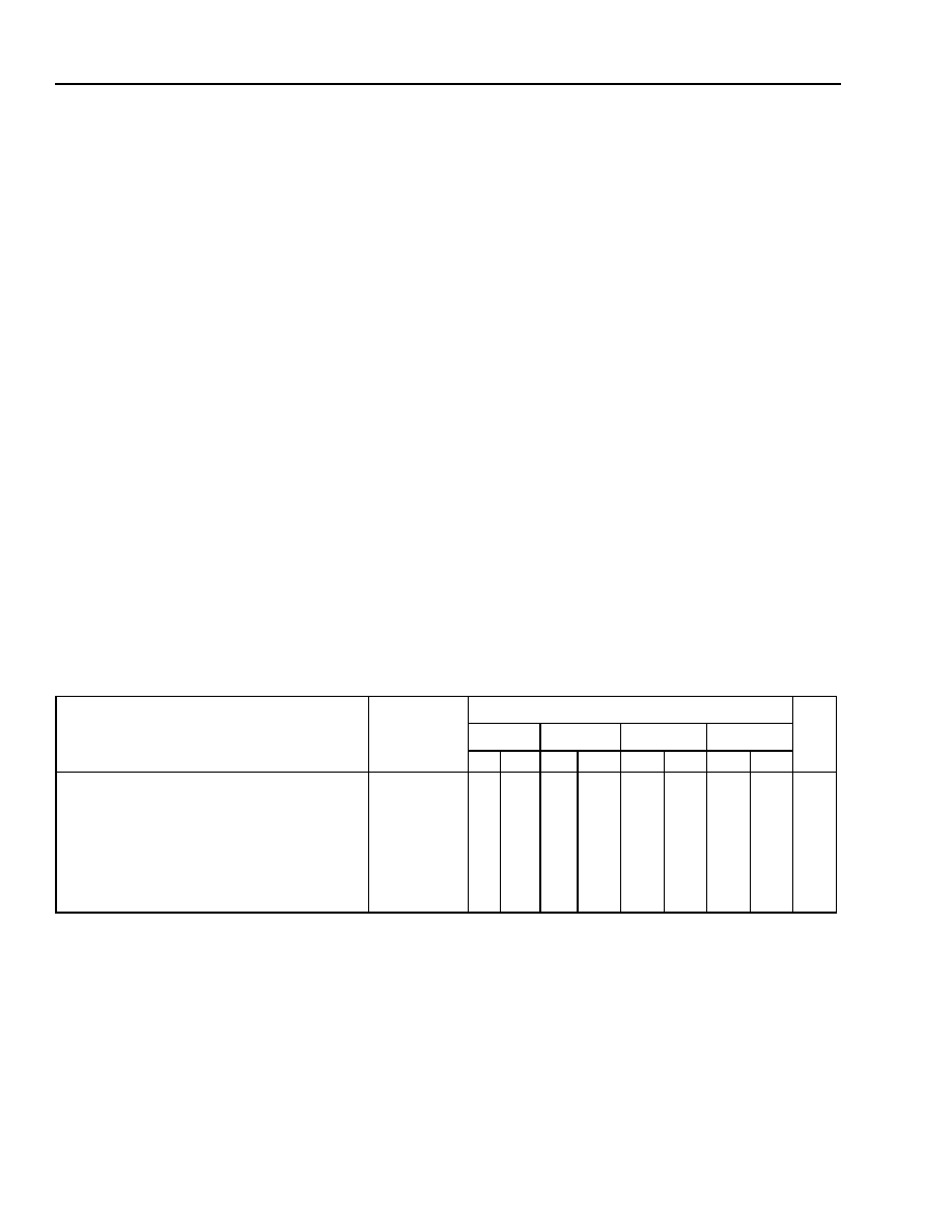
104
104
Lucent Technologies Inc.
Data Sheet
June 1999
ORCA Series 3C and 3T FPGAs
Timing Characteristics
(continued)
In addition to supply voltage, process variation, and
operating temperature, circuit and process improve-
ments of the
ORCA
Series FPGAs over time will result
in significant improvement of the actual performance
over those listed for a speed grade. Even though lower
speed grades may still be available, the distribution of
yield to timing parameters may be several speed
grades higher than that designated on a product brand.
Design practices need to consider best-case timing
parameters (e.g., delays = 0), as well as worst-case
timing.
The routing delays are a function of fan-out and the
capacitance associated with the CIPs and metal inter-
connect in the path. The number of logic elements that
can be driven (fan-out) by PFUs is unlimited, although
the delay to reach a valid logic level can exceed timing
requirements. It is difficult to make accurate routing
delay estimates prior to design compilation based on
fan-out. This is because the CAE software may delete
redundant logic inserted by the designer to reduce fan-
out, and/or it may also automatically reduce fan-out by
net splitting.
The waveform test points are given in the Input/Output
Buffer Measurement Conditions section of this data
sheet. The timing parameters given in the electrical
characteristics tables in this data sheet follow industry
practices, and the values they reflect are described
below.
Propagation Delay--The time between the specified
reference points. The delays provided are the worst
case of the tphh and tpll delays for noninverting func-
tions, tplh and tphl for inverting functions, and tphz and
tplz for 3-state enable.
Setup Time--The interval immediately preceding the
transition of a clock or latch enable signal, during which
the data must be stable to ensure it is recognized as
the intended value.
Hold Time--The interval immediately following the
transition of a clock or latch enable signal, during which
the data must be held stable to ensure it is recognized
as the intended value.
3-State Enable--The time from when a 3-state control
signal becomes active and the output pad reaches the
high-impedance state.
PFU Timing
* Four-input variables' (K
Z
[3:0]) path delays are valid for LUTs in both F4 (four-input LUT) and F5 (five-input LUT) modes.
Table 41. Combinatorial PFU Timing Characteristics
OR3Cxx Commercial: V
DD
= 5.0 V ± 5%, 0 ∞C
<
T
A
<
70 ∞C; Industrial: V
DD
= 5.0 V ± 10%, ≠40 ∞C
<
T
A
<
+85 ∞C.
OR3Txxx Commercial: V
DD
= 3.0 V to 3.6 V, 0 ∞C
<
T
A
<
70 ∞C; Industrial: V
DD
= 3.0 V to 3.6 V, ≠40 ∞C
<
T
A
<
+85 ∞C.
Parameter
Symbol
Speed
Unit
-4
-5
-6
-7
Min Max Min
Max
Min
Max
Min
Max
Combinatorial Delays (T
J
= +85 ∞C, V
DD
= min):
Four-input Variables (Kz[3:0] to F[z])*
Five-input Variables (F5[A:D] to F[0, 2, 4, 6])
Two-level LUT Delay (Kz[3:0] to F w/feedbk)*
Two-level LUT Delay (F5[A:D] to F w/feedbk)
Three-level LUT Delay (Kz[3:0] to F w/feedbk)*
Three-level LUT Delay (F5[A:D] to F w/feedbk)
C
IN
to C
OUT
Delay (logic mode)
F4_DEL
F5_DEL
SWL2_DEL
SWL2F5_DEL
SWL3_DEL
SWL3F5_DEL
CO_DEL
--
--
--
--
--
--
--
2.34
2.11
4.87
4.69
6.93
6.89
3.47
--
--
--
--
--
--
--
1.80
1.57
3.66
3.51
5.15
5.08
2.65
--
--
--
--
--
--
--
1.32
1.23
2.58
2.48
3.63
3.54
1.79
--
--
--
--
--
--
--
1.05
0.99
2.03
1.94
2.82
2.75
1.43
ns
ns
ns
ns
ns
ns
ns
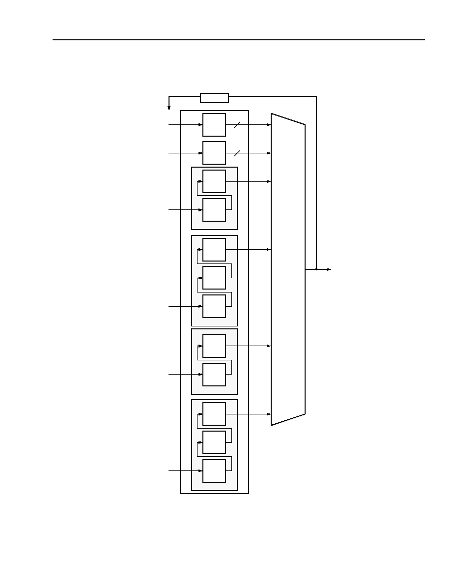
Lucent Technologies Inc.
105
Data Sheet
June 1999
ORCA Series 3C and 3T FPGAs
Timing Characteristics
(continued)
Note: See Table 46 for an explanation of FDBK_DEL and OMUX_DEL.
5-5751(F)
Figure 64. Combinatorial PFU Timing
F4_DEL
LUT
F4_DEL/
F5_DEL
LUT
F5≠DEL
LUT
F4_DEL/
LUT
F4_DEL/
F5_DEL
LUT
F4_DEL/
F5_DEL
LUT
F4_DEL/
LUT
F4_DEL/
F5_DEL
LUT
F4_DEL/
F5_DEL
LUT
F4_DEL/
F5_DEL
LUT
F4_DEL/
F5_DEL
LUT
F4_DEL/
F5_DEL
LUT
K
Z
[3:0]
K
Z
[3:0], F5[A:D]
K
Z
[3:0]
K
Z
[3:0]
F5[A:D]
F5[A:D]
F[7:0]
F[6, 4,
F[7:0]
F[7:0]
F[7:0]
F[7:0]
FDBK≠DEL
O[9:0]
SWL2_DEL
SWL3_DEL
SWL2F5_DEL
SWL3F5_DEL
PFU
8
4
OMUX_DEL
2, 0]
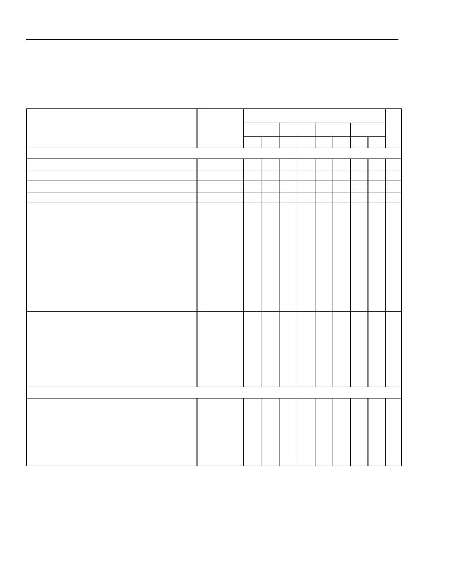
106
Lucent Technologies Inc.
Data Sheet
June 1999
ORCA Series 3C and 3T FPGAs
Timing Characteristics
(continued)
Table 42. Sequential PFU Timing Characteristics
OR3Cxx Commercial: V
DD
= 5.0 V ± 5%, 0 ∞C
<
T
A
<
70 ∞C; Industrial: V
DD
= 5.0 V ± 10%, ≠40 ∞C
<
T
A
<
+85 ∞C.
OR3Txxx Commercial: V
DD
= 3.0 V to 3.6 V, 0 ∞C
<
T
A
<
70 ∞C; Industrial: V
DD
= 3.0 V to 3.6 V, ≠40 ∞C
<
T
A
<
+85 ∞C
.
Parameter
Symbol
Speed
Unit
-4
-5
-6
-7
Min Max
Min Max Min Max Min Max
Input Requirements
Clock Low Time
CLKL_MPW
3.36
--
2.07
--
0.94
--
0.72
--
ns
Clock High Time
CLKH_MPW
1.61
--
1.06
--
0.54
--
0.45
--
ns
Global S/R Pulse Width (GSRN)
GSR_MPW
3.36
--
2.07
--
0.94
--
0.72
--
ns
Local S/R Pulse Width
LSR_MPW
3.36
--
2.07
--
0.94
--
0.72
--
ns
Combinatorial Setup Times (T
J
= +85 ∞C, V
DD
= min):
Four-input Variables to Clock (Kz[3:0] to CLK)*
Five-input Variables to Clock (F5[A:D] to CLK)
Data In to Clock (DIN[7:0] to CLK)
Carry-in to Clock, DIRECT to REGCOUT (CIN to CLK)
Clock Enable to Clock (CE to CLK)
Clock Enable to Clock (ASWE to CLK)
Local Set/Reset to Clock (SYNC) (LSR to CLK)
Data Select to Clock (SEL to CLK)
Two-level LUT to Clock (Kz[3:0] to CLK w/feedbk)*
Two-level LUT to Clock (F5[A:D] to CLK w/feedbk)
Three-level LUT to Clock (Kz[3:0] to CLK w/feedbk)*
Three-level LUT to Clock (F5[A:D] to CLK w/feedbk)
F4_SET
F5_SET
DIN_SET
CINDIR_SET
CE1_SET
CE2_SET
LSR_SET
SEL_SET
SWL2_SET
SWL2F5_SET
SWL3_SET
SWL3F5_SET
1.99
1.79
0.47
1.25
2.86
1.68
1.86
1.37
3.98
4.06
6.49
6.39
--
--
--
--
--
--
--
--
--
--
--
--
1.47
1.33
0.32
0.99
2.15
1.30
1.36
1.00
2.99
2.97
4.81
4.73
--
--
--
--
--
--
--
--
--
--
--
--
1.08
1.03
0.18
0.71
1.80
0.95
0.86
0.92
2.13
2.29
3.42
3.34
--
--
--
--
--
--
--
--
--
--
--
--
0.85
0.81
0.16
0.58
1.37
0.77
0.68
0.70
1.63
1.68
2.64
2.57
--
--
--
--
--
--
--
--
--
--
--
--
ns
ns
ns
ns
ns
ns
ns
ns
ns
ns
ns
ns
Combinatorial Hold Times (T
J
= all, V
DD
= all):
Data In (DIN[7:0] from CLK)
Carry-in from Clock, DIRECT to REGCOUT (CIN from
CLK)
Clock Enable (CE from CLK)
Clock Enable from Clock (ASWE from CLK)
Local Set/Reset from Clock (sync) (LSR from CLK)
Data Select from Clock (SEL from CLK)
All Others
DIN_HLD
CINDIR_HLD
CE1_HLD
CE2_HLD
LSR_HLD
SEL_HLD
--
0.00
0.00
0.00
0.00
0.00
0.00
0.00
--
--
--
--
--
--
--
0.00
0.00
0.00
0.00
0.00
0.00
0.00
--
--
--
--
--
--
--
0.00
0.00
0.00
0.00
0.00
0.00
0.00
--
--
--
--
--
--
--
0.00
0.00
0.00
0.00
0.00
0.00
0.00
--
--
--
--
--
--
--
ns
ns
ns
ns
ns
ns
ns
Output Characteristics
Sequential Delays (T
J
= +85 ∞C, V
DD
= min):
Local S/R (async) to PFU Out (LSR to Q[7:0], REG-
COUT)
Global S/R to PFU Out (GSRN to Q[7:0], REGCOUT)
Clock to PFU Out--Register (CLK to Q[7:0], REG-
COUT)
Clock to PFU Out--Latch (CLK to Q[7:0])
Transparent Latch (DIN[7:0] to Q[7:0])
LSR_DEL
GSR_DEL
REG_DEL
LTCH_DEL
LTCHD_DEL
--
--
--
--
--
7.02
5.21
2.38
2.51
2.73
--
--
--
--
--
5.29
3.90
1.75
1.88
2.10
--
--
--
--
--
3.64
2.55
1.26
1.21
1.38
--
--
--
--
--
2.90
2.00
0.97
0.96
1.12
ns
ns
ns
ns
ns
* Four-input variables' (K
Z
[3:0]) setup times are valid for LUTs in both F4 (four-input LUT) and F5 (five-input LUT) modes.
Note: The table shows worst-case delays.
ORCA
Foundry reports the delays for individual paths within a group of paths representing the same
timing parameter and may accurately report delays that are less than those listed.

Lucent Technologies Inc.
107
Data Sheet
June 1999
ORCA Series 3C and 3T FPGAs
Timing Characteristics
(continued)
Table 43. Ripple Mode PFU Timing Characteristics
OR3Cxx Commercial: V
DD
= 5.0 V ± 5%, 0 ∞C
<
T
A
<
70 ∞C; Industrial: V
DD
= 5.0 V ± 10%, ≠40 ∞C
<
T
A
<
+85 ∞C.
OR3Txxx Commercial: V
DD
= 3.0 V to 3.6 V, 0 ∞C
<
T
A
<
70 ∞C; Industrial: V
DD
= 3.0 V to 3.6 V, ≠40 ∞C
<
T
A
<
+85 ∞C
.
Parameter
(T
J
= +85 ∞C, V
DD
= min)
Symbol
Speed
Unit
-4
-5
-6
-7
Min Max Min Max Min Max Min Max
Full Ripple Setup Times (byte wide):
Operands to Clock (Kz[1:0] to CLK)
Bitwise Operands to Clock (Kz[1:0] to CLK at F[z])
Fast Carry-in to Clock (FCIN to CLK)
Carry-in to Clock (CIN to CLK)
Add/Subtract to Clock (ASWE to CLK)
Operands to Clock (Kz[1:0] to CLK at REGCOUT)
Fast Carry-in to Clock (FCIN to CLK at REGCOUT)
Carry-in to Clock (CIN to CLK at REGCOUT)
Add/Subtract to Clock (ASWE to CLK at REGCOUT)
RIP_SET
FRIP_SET
FCIN_SET
CIN_SET
AS_SET
RIPRC_SET
FCINRC_SET
CINRC_SET
ASRC_SET
3.50
1.99
2.55
3.80
8.82
2.09
2.29
3.09
8.14
--
--
--
--
--
--
--
--
--
2.50
1.47
1.87
2.79
6.18
1.61
1.76
2.36
5.73
--
--
--
--
--
--
--
--
--
1.96
1.08
1.34
1.97
4.68
1.19
1.28
1.73
4.54
--
--
--
--
--
--
--
--
--
1.48
0.85
1.04
1.56
3.50
0.93
1.02
1.35
3.39
--
--
--
--
--
--
--
--
--
ns
ns
ns
ns
ns
ns
ns
ns
ns
Full Ripple Hold Times (T
J
= all, V
DD
= all):
Fast Carry-in from Clock (FCIN from CLK at REG-
COUT)
All Others
FCINRC_HLD
GENERIC_HLD
0.00
0.00
--
--
0.00
0.00
--
--
0.00
0.00
--
--
0.00
0.00
--
--
ns
ns
Half Ripple Setup Times (nibble wide):
Operands to Clock (Kz[1:0] to CLK)
Bitwise Operands to Clock (Kz[1:0] to CLK at F[z])
Fast Carry-in to Clock (FCIN to CLK)
Carry-in to Clock (CIN to CLK)
Add/Subtract to Clock (ASWE to CLK)
Operands to Clock (Kz[1:0] to CLK at REGCOUT)
Fast Carry-in to Clock (FCIN to CLK at REGCOUT)
Carry-in to Clock (CIN to CLK at REGCOUT)
Add/Subtract to Clock (ASWE to CLK at REGCOUT)
HRIP_SET
HFRIP_SET
HFCIN_SET
HCIN_SET
HAS_SET
HRIPRC_SET
HFCINRC_SET
HCINRC_SET
HASRC_SET
3.91
1.99
2.55
3.80
8.82
3.03
2.29
3.09
8.14
--
--
--
--
--
--
--
--
--
2.81
1.47
1.87
2.79
6.18
2.31
1.76
2.36
5.73
--
--
--
--
--
--
--
--
--
2.21
1.08
1.34
1.97
4.68
1.68
1.28
1.73
4.54
--
--
--
--
--
--
--
--
--
1.66
0.85
1.04
1.56
3.50
1.32
1.02
1.35
3.39
--
--
--
--
--
--
--
--
--
ns
ns
ns
ns
ns
ns
ns
ns
ns
Half Ripple Hold Times (T
J
= all, V
DD
= all):
Fast Carry-in from Clock (HFCIN from CLK at REG-
COUT)
All Others
HFCINRC_HLD
GENERIC_HLD
0.00
0.00
--
--
0.00
0.00
--
--
0.00
0.00
--
--
0.00
0.00
--
--
ns
ns
Note: The table shows worst-case delay for the ripple chain.
ORCA
Foundry reports the delay for individual paths within the ripple chain that
will be less than or equal to those listed above.

108
Lucent Technologies Inc.
Data Sheet
June 1999
ORCA Series 3C and 3T FPGAs
Timing Characteristics
(continued)
Table 43. Ripple Mode PFU Timing Characteristics (continued)
OR3Cxx Commercial: V
DD
= 5.0 V ± 5%, 0 ∞C
<
T
A
<
70 ∞C; Industrial: V
DD
= 5.0 V ± 10%, ≠40 ∞C
<
T
A
<
+85 ∞C.
OR3Txxx Commercial: V
DD
= 3.0 V to 3.6 V, 0 ∞C
<
T
A
<
70 ∞C; Industrial: V
DD
= 3.0 V to 3.6 V, ≠40 ∞C
<
T
A
<
+85 ∞C
.
Parameter
(T
J
= +85 ∞C, V
DD
= min)
Symbol
Speed
Unit
-4
-5
-6
-7
Min
Max
Min Max
Min
Max
Min
Max
Full Ripple Delays (byte wide):
Operands to Carry-out (Kz[1:0] to COUT)
Operands to Carry-out (Kz[1:0] to FCOUT)
Operands to PFU Out (Kz[1:0] to F[7:0])
Bitwise Operands to PFU Out (Kz[1:0] to F[z])
Fast Carry-in to Carry-out (FCIN to COUT)
Fast Carry-in to Fast
Carry-out (FCIN to FCOUT)
Carry-in to Carry-out (CIN to COUT)
Carry-in to Fast Carry-out (CIN to FCOUT)
Fast Carry-in PFU Out (FCIN to F[7:0])
Carry-in PFU Out (CIN to F[7:0])
Add/Subtract to Carry-out (ASWE to COUT)
Add/Subtract to Carry-out (ASWE to FCOUT)
Add/Subtract to PFU Out (ASWE to F[7:0])
RIPCO_DEL
RIPFCO_DEL
RIP_DEL
FRIP_DEL
FCINCO_DEL
FCINFCO_DEL
CINCO_DEL
CINFCO_DEL
FCIN_DEL
CIN_DEL
ASCO_DEL
ASFCO_DEL
AS_DEL
--
--
--
--
--
--
--
--
--
--
--
--
--
5.32
5.30
7.37
2.34
2.59
2.57
3.47
3.46
6.03
6.91
8.28
8.11
10.66
--
--
--
--
--
--
--
--
--
--
--
--
--
4.11
4.10
5.60
1.80
1.99
1.98
2.65
2.64
4.55
5.21
5.89
5.78
7.55
--
--
--
--
--
--
--
--
--
--
--
--
--
2.98
2.98
4.18
1.32
1.43
1.41
1.79
1.78
3.21
3.53
4.58
4.48
5.85
--
--
--
--
--
--
--
--
--
--
--
--
--
2.32
2.32
3.10
1.05
1.14
1.13
1.43
1.43
2.51
3.05
3.45
3.38
4.38
ns
ns
ns
ns
ns
ns
ns
ns
ns
ns
ns
ns
ns
Half Ripple Delays (nibble wide):
Operands to Carry-out (Kz[1:0] to COUT)
Operands to Fast Carry-out (Kz[1:0] to FCOUT)
Operands to PFU Out (Kz[1:0] to F[3:0])
Bitwise Operands to PFU Out (Kz[1:0] to F[z])
Fast Carry-in to Carry-out (FCIN to COUT)
Fast Carry-in to Fast Carry-out (FCIN to FCOUT)
Carry-in to Carry-out (CIN to COUT)
Carry-in to Carry-out (CIN to FCOUT)
Fast Carry-in PFU Out (FCIN to F[3:0])
Carry-in PFU Out (CIN to F[3:0])
Add/Subtract to Carry-out (ASWE to COUT)
Add/Subtract to Carry-out (ASWE to FCOUT)
Add/Subtract to PFU Out (ASWE to F[3:0])
HRIPCO_DEL
HRIPFCO_DEL
HRIP_DEL
HFRIP_DEL
HFCINCO_DEL
HFCINFCO_DEL
HCINCO_DEL
HCINFCO_DEL
HFCIN_DEL
HCIN_DEL
HASCO_DEL
HASFCO_DEL
HAS_DEL
--
--
--
--
--
--
--
--
--
--
--
--
--
5.32
5.30
5.50
2.34
2.59
2.57
3.47
3.46
3.76
4.65
8.28
8.11
9.12
--
--
--
--
--
--
--
--
--
--
--
--
--
4.11
4.10
4.07
1.80
1.99
1.98
2.65
2.64
2.84
3.50
5.89
5.78
6.49
--
--
--
--
--
--
--
--
--
--
--
--
--
2.98
2.98
3.20
1.32
1.43
1.41
1.79
1.78
2.01
2.33
4.58
4.48
4.86
--
--
--
--
--
--
--
--
--
--
--
--
--
2.32
2.32
2.40
1.05
1.14
1.13
1.43
1.43
1.58
2.12
3.45
3.38
3.69
ns
ns
ns
ns
ns
ns
ns
ns
ns
ns
ns
ns
ns
Note: The table shows worst-case delay for the ripple chain.
ORCA
Foundry reports the delay for individual paths within the ripple chain that will
be less than or equal to those listed above.
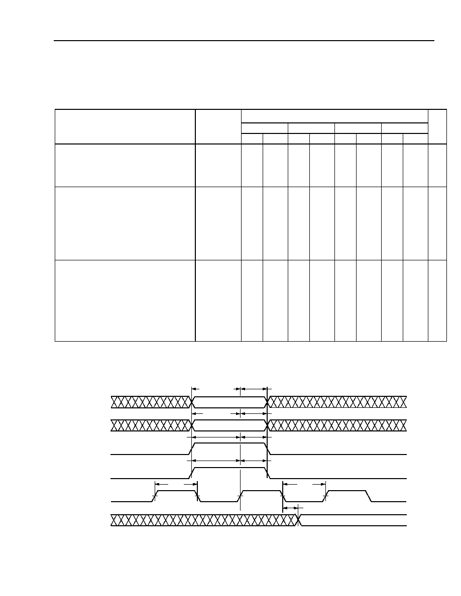
Lucent Technologies Inc.
109
Data Sheet
June 1999
ORCA Series 3C and 3T FPGAs
Timing Characteristics
(continued)
Table 44. Synchronous Memory Write Characteristics
OR3Cxx Commercial: V
DD
= 5.0 V ± 5%, 0 ∞C
<
T
A
<
70 ∞C; Industrial: V
DD
= 5.0 V ± 10%, ≠40 ∞C
<
T
A
<
+85 ∞C.
OR3Txxx Commercial: V
DD
= 3.0 V to 3.6 V, 0 ∞C
<
T
A
<
70 ∞C; Industrial: V
DD
= 3.0 V to 3.6 V, ≠40 ∞C
<
T
A
<
+85 ∞C.
* The RAM is written on the inactive clock edge following the active edge that latches the address, data, and control signals.
Note: The table shows worst-case delays.
ORCA
Foundry reports the delays for individual paths within a group of paths representing the same
timing parameter and may accurately report delays that are less than those listed.
5-4621(F)
Figure 65. Synchronous Memory Write Characteristics
Parameter
Symbol
Speed
Unit
-4
-5
-6
-7
Min
Max
Min
Max
Min
Max
Min
Max
Write Operation for RAM Mode:
Maximum Frequency
Clock Low Time
Clock High Time
Clock to Data Valid (CLK to F[6, 4, 2, 0])*
SMCLK_FRQ
SMCLKL_MPW
SMCLKH_MPW
MEM_DEL
--
2.34
3.79
--
151.00
--
--
10.00
--
1.80
2.77
--
197.00
--
--
7.14
--
1.32
2.13
--
254.00
--
--
5.00
--
1.05
1.62
--
315.00
4.08
MHz
ns
ns
ns
Write Operation Setup Time:
Address to Clock (CIN to CLK)
Address to Clock (DIN[7, 5, 3, 1] to CLK)
Data to Clock (DIN[6, 4, 2, 0] to CLK)
Write Enable (WREN) to Clock (ASWE to CLK)
Write-port Enable 0 (WPE0) to Clock (CE to
CLK)
Write-port Enable 1 (WPE1) to Clock (LSR to
CLK)
WA4_SET
WA_SET
WD_SET
WE_SET
WPE0_SET
WPE1_SET
1.25
0.72
0.02
0.18
2.25
2.79
--
--
--
--
--
--
0.99
0.52
0.06
0.16
1.69
2.13
--
--
--
--
--
--
0.71
0.35
0.00
0.14
1.16
1.58
--
--
--
--
--
--
0.58
0.28
0.00
0.12
0.84
1.31
--
--
--
--
--
--
ns
ns
ns
ns
ns
ns
Write Operation Hold Time:
Address from Clock (CIN from CLK)
Address from Clock (DIN[7, 5, 3, 1] from CLK)
Data from Clock (DIN[6, 4, 2, 0] from CLK)
Write Enable (WREN) from Clock (ASWE from
CLK)
Write-port Enable 0 (WPE0) from Clock (CE
from CLK)
Write-port Enable 1 (WPE1) from Clock (LSR
from CLK)
WA4_HLD
WA_HLD
WD_HLD
WE_HLD
WPE0_HLD
WPE1_HLD
0.00
0.00
0.59
0.03
0.00
0.00
--
--
--
--
--
--
0.00
0.00
0.42
0.00
0.00
0.00
--
--
--
--
--
--
0.00
0.00
0.40
0.08
0.00
0.00
--
--
--
--
--
--
0.00
0.00
0.32
0.06
0.00
0.00
--
--
--
--
--
--
ns
ns
ns
ns
ns
ns
CK
F[6, 4, 2, 0]
CIN, DIN[7, 5, 3, 1]
DIN[6, 4, 2, 0]
MEM_DEL
WA4_SET
ASWE (WREN)
CE (WPE0),
T
SCH
T
SCL
WA4_HLD
WD_SET
WD_HLD
WE_SET
WE_HLD
WPE0_SET
WPE0_HLD
WA_SET
WA_HLD
WPE1_SET
WPE1_HLD
LSR (WPE1)
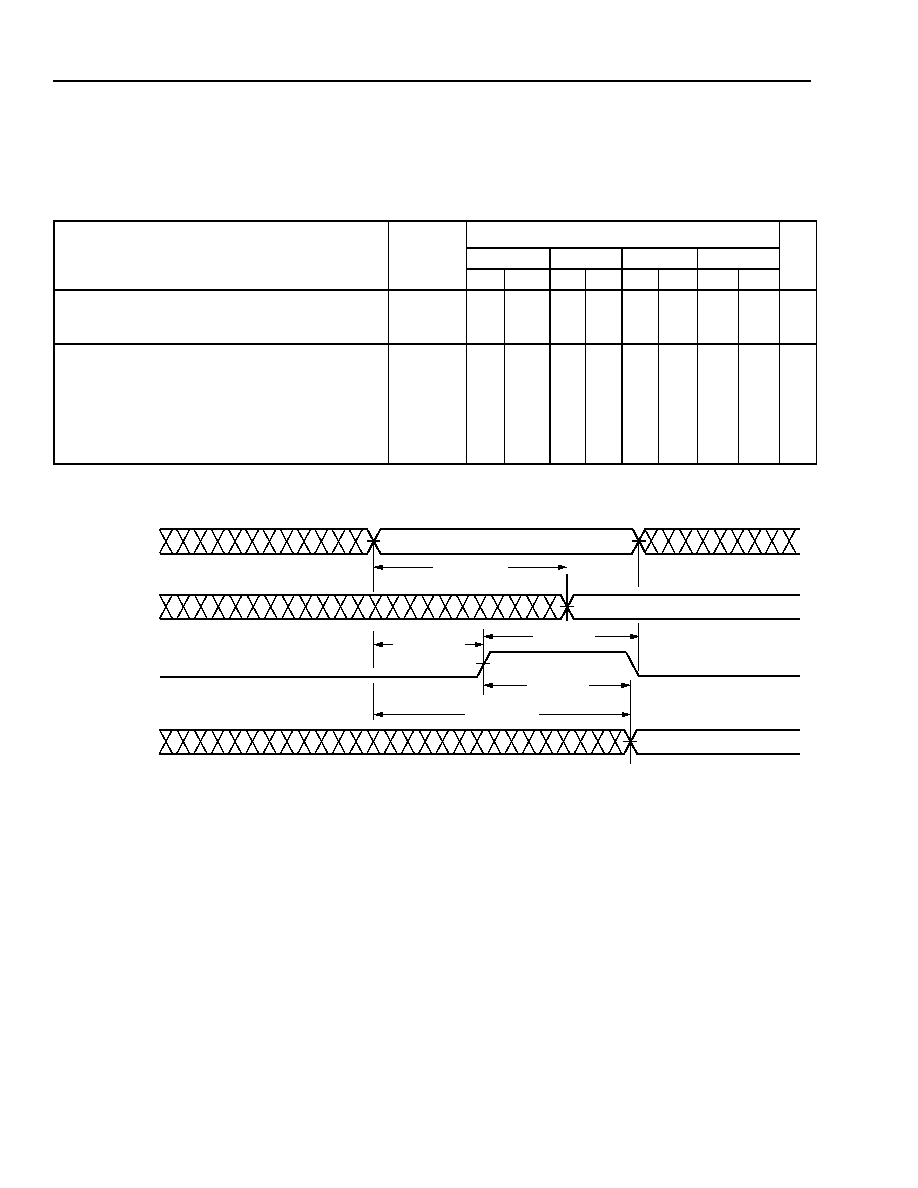
110
Lucent Technologies Inc.
Data Sheet
June 1999
ORCA Series 3C and 3T FPGAs
Timing Characteristics
(continued)
Table 45. Synchronous Memory Read Characteristics
OR3Cxx Commercial: V
DD
= 5.0 V ± 5%, 0 ∞C
<
T
A
<
70 ∞C; Industrial: V
DD
= 5.0 V ± 10%, ≠40 ∞C
<
T
A
<
+85 ∞C.
OR3Txxx Commercial: V
DD
= 3.0 V to 3.6 V, 0 ∞C
<
T
A
<
70 ∞C; Industrial: V
DD
= 3.0 V to 3.6 V, ≠40 ∞C
<
T
A
<
+85 ∞C.
Note: The table shows worst-case delays.
ORCA
Foundry reports the delays for individual paths within a group of paths representing the same
timing parameter and may accurately report delays that are less than those listed.
5-4622(F)
Figure 66. Synchronous Memory Read Cycle
Parameter
(T
J
= 85 ∞C, V
DD
= min)
Symbol
Speed
Unit
-4
-5
-6
-7
Min
Max
Min Max Min
Max
Min
Max
Read Operation:
Data Valid After Address (Kz[3:0] to F[6, 4, 2, 0])
Data Valid After Address (F5[A:D] to F[6, 4, 2, 0])
RA_DEL
RA4_DEL
--
--
2.34
2.11
--
--
1.80
1.57
--
--
1.32
1.23
--
--
1.05
0.99
ns
ns
Read Operation, Clocking Data into Latch/FF:
Address to Clock Setup Time (Kz[3:0] to CLK)
Address to Clock Setup Time (F5[A:D] to CLK)
Address from Clock Hold Time (Kz[3:0] from CLK)
Address from Clock Hold Time (F5[A:D] from CLK)
Clock to PFU Output--Register (CLK to Q[6, 4, 2, 0])
Read Cycle Delay
RA_SET
RA4_SET
RA_HLD
RA4_HLD
REG_DEL
SMRD_CYC
1.99
1.79
0.00
0.00
--
--
--
--
--
--
2.38
10.48
1.47
1.33
0.00
0.00
--
--
--
--
--
--
1.75
7.66
1.08
1.03
0.00
0.00
--
--
--
--
--
--
1.26
7.53
0.85
0.81
0.00
0.00
--
--
--
--
--
--
0.97
5.78
ns
ns
ns
ns
ns
ns
Kz[3:0], F5[A:D]
F[6, 4, 2, 0]
CLK
Q[3:0]
RA_DEL
RA4_DEL
RA_SET
RA4_SET
REG_DEL
RA_HLD
RA4_HLD
SMRD_CYC
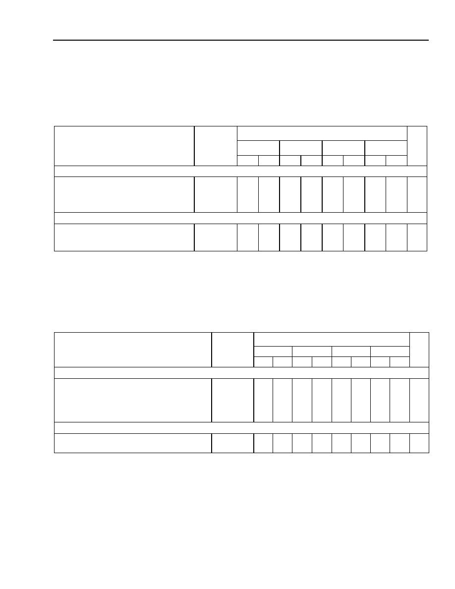
Lucent Technologies Inc.
111
Data Sheet
June 1999
ORCA Series 3C and 3T FPGAs
Timing Characteristics
(continued)
PLC Timing
Table 46. PFU Output MUX and Direct Routing Timing Characteristics
OR3Cxx Commercial: V
DD
= 5.0 V ± 5%, 0 ∞C
<
T
A
<
70 ∞C; Industrial: V
DD
= 5.0 V ± 10%, ≠40 ∞C
<
T
A
<
+85 ∞C.
OR3Txxx Commercial: V
DD
= 3.0 V to 3.6 V, 0 ∞C
<
T
A
<
70 ∞C; Industrial: V
DD
= 3.0 V to 3.6 V, ≠40 ∞C
<
T
A
<
+85 ∞C.
* This is general feedback using switching segments. See the combinatorial PFU timing table for softwired look-up table feedback timing.
SLIC Timing
Table 47. Supplemental Logic and Interconnect Cell (SLIC) Timing Characteristics
OR3Cxx Commercial: V
DD
= 5.0 V ± 5%, 0 ∞C
<
T
A
<
70 ∞C; Industrial: V
DD
= 5.0 V ± 10%, ≠40 ∞C
<
T
A
<
+85 ∞C.
OR3Txxx Commercial: V
DD
= 3.0 V to 3.6 V, 0 ∞C
<
T
A
<
70 ∞C; Industrial: V
DD
= 3.0 V to 3.6 V, ≠40 ∞C
<
T
A
<
+85 ∞C.
Parameter
(T
J
= 85 ∞C, V
DD
= min)
Symbol
Speed
Unit
-4
-5
-6
-7
Min
Max
Min
Max
Min
Max
Min
Max
PFU Output MUX (Fan-out = 1)
Output MUX Delay (F[7:0]/Q[7:0] to O[9:0])
Carry-out MUX Delay (COUT to O9)
Registered Carry-out MUX Delay (REGCOUT
to O8)
OMUX_DEL
COO9_DEL
RCOO8_DEL
--
--
--
0.50
0.34
0.34
--
--
--
0.39
0.26
0.26
--
--
--
0.35
0.24
0.24
--
--
--
0.28
0.18
0.18
ns
ns
ns
Direct Routing
PFU Feedback (xSW)*
PFU to Orthogonal PFU Delay (xSW to xSW)
PFU to Diagonal PFU Delay (xBID to xSW)
FDBK_DEL
ODIR_DEL
DDIR_DEL
--
--
--
1.74
2.21
2.69
--
--
--
1.41
1.77
2.19
--
--
--
1.48
1.75
2.53
--
--
--
1.14
1.39
1.98
ns
ns
ns
Parameter
(T
J
= 85 ∞C, V
DD
= min)
Symbol
Speed
Unit
-4
-5
-6
-7
Min
Max
Min
Max
Min
Max
Min
Max
3-Statable BIDIs
BIDI Delay (BRx to BLx, BLx to BRx)
BIDI Delay (Ox to BRx, Ox to BLx)
BIDI 3-state Enable/Disable Delay (TRI to BL, BR)
BIDI 3-state Enable/Disable Delay
(BL, BR via DEC, TRI to BL, BR)
BUF_DEL
OBUF_DEL
TRI_DEL
DECTRI_DEL
--
--
--
--
0.84
0.72
2.55
3.59
--
--
--
--
0.70
0.61
1.90
2.65
--
--
--
--
0.94
0.87
1.31
1.91
--
--
--
--
0.77
0.70
1.01
1.48
ns
ns
ns
ns
Decoder
Decoder Delay (BR[9:8], BL[9:8] to DEC)
Decoder Delay (BR[7:0], BL[7:0] to DEC)
DEC98_DEL
DEC_DEL
--
--
2.39
2.35
--
--
1.85
1.82
--
--
1.27
1.23
--
--
1.02
0.99
ns
ns
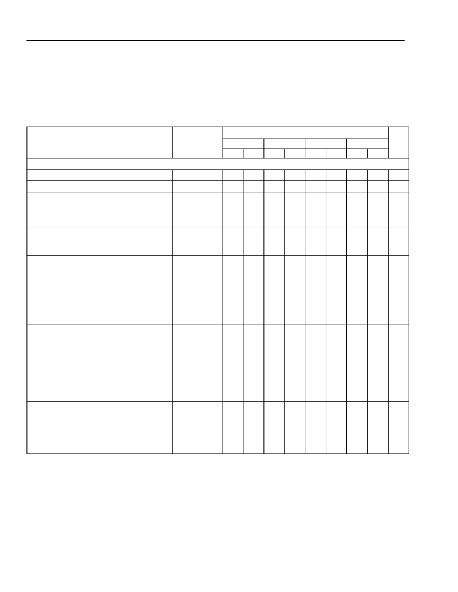
112
Lucent Technologies Inc.
Data Sheet
June 1999
ORCA Series 3C and 3T FPGAs
Timing Characteristics
(continued)
PIO Timing
Table 48. Programmable I/O (PIO) Timing Characteristics
OR3Cxx Commercial: V
DD
= 5.0 V ± 5%, 0 ∞C
<
T
A
<
70 ∞C; Industrial: V
DD
= 5.0 V ± 10%, ≠40 ∞C
<
T
A
<
+85 ∞C.
OR3Txxx Commercial: V
DD
= 3.0 V to 3.6 V, 0 ∞C
<
T
A
<
70 ∞C; Industrial: V
DD
= 3.0 V to 3.6 V, ≠40 ∞C
<
T
A
<
+85
∞C.
Parameter
Symbol
Speed
Unit
-4
-5
-6
-7
Min
Max
Min
Max
Min
Max
Min
Max
Input Delays (T
J
= 85 ∞C, V
DD
= min)
Input Rise Time
IN_RIS
--
500
--
500
--
500
--
500
ns
Input Fall Time
IN_FAL
--
500
--
500
--
500
--
500
ns
PIO Direct Delays:
Pad to In (pad to CLK IN)
Pad to In (pad to IN1, IN2)
Pad to In Delayed (pad to IN1, IN2)
CKIN_DEL
IN_DEL
IND_DEL
--
--
--
1.41
2.16
9.05
--
--
--
1.26
1.87
7.83
--
--
--
0.64
1.28
6.64
--
--
--
0.41
0.90
7.27
ns
ns
ns
PIO Transparent Latch Delays:
Pad to In (pad to IN1, IN2)
Pad to In Delayed (pad to IN1, IN2)
LATCH_DEL
LATCHD_DEL
--
--
4.11
10.58
--
--
3.25
9.05
--
--
2.52
7.67
--
--
1.82
7.65
ns
ns
Input Latch/FF Setup Timing:
Pad to ExpressCLK (fast-capture latch/FF)
Pad Delayed to ExpressCLK
(fast-capture latch/FF)
Pad to Clock (input latch/FF)
Pad Delayed to Clock (input latch/FF)
Clock Enable to Clock (CE to CLK)
Local Set/Reset (sync) to Clock (LSR to CLK)
INREGE_SET
INREGED_SET
INREG_SET
INREGD_SET
INCE_SET
INLSR_SET
5.93
12.86
1.62
8.57
2.03
1.79
--
--
--
--
--
--
4.82
11.03
1.42
7.36
1.64
1.45
--
--
--
--
--
--
3.63
9.18
0.71
5.91
1.29
1.14
--
--
--
--
--
--
3.23
9.68
0.50
7.06
1.00
0.89
--
--
--
--
--
--
ns
ns
ns
ns
ns
ns
Input FF/Latch Hold Timing:
Pad from ExpressCLK (fast-capture latch/FF)
Pad Delayed from ExpressCLK
(fast-capture latch/FF)
Pad from Clock (input latch/FF)
Pad Delayed from Clock (input latch/FF)
Clock Enable from Clock (CE from CLK)
Local Set/Reset (sync) from Clock
(LSR from CLK)
INREGE_HLD
INREGED_HLD
INREG_HLD
INREGD_HLD
INCE_HLD
INLSR_HLD
0.00
0.00
0.00
0.00
0.00
0.00
--
--
--
--
--
--
0.00
0.00
0.00
0.00
0.00
0.00
--
--
--
--
--
--
0.00
0.00
0.00
0.00
0.00
0.00
--
--
--
--
--
--
0.00
0.00
0.00
0.00
0.00
0.00
--
--
--
--
--
--
ns
ns
ns
ns
ns
ns
Clock-to-in Delay (FF CLK to IN1, IN2)
Clock-to-in Delay (latch CLK to IN1, IN2)
Local S/R (async) to IN (LSR to IN1, IN2)
Local S/R (async) to IN (LSR to IN1, IN2)
LatchFF in Latch Mode
Global S/R to In (GSRN to IN1, IN2)
INREG_DEL
INLTCH_DEL
INLSR_DEL
INLSRL_DEL
INGSR_DEL
--
--
--
--
--
4.05
4.08
6.11
5.89
5.38
--
--
--
--
--
3.14
3.19
4.76
4.66
4.22
--
--
--
--
--
2.53
2.62
3.81
3.57
3.44
--
--
--
--
--
2.05
2.14
3.17
2.98
2.88
ns
ns
ns
ns
ns
Note: The delays for all input buffers assume an input rise/fall time of
<
1 V/ns.

Lucent Technologies Inc.
113
Data Sheet
June 1999
ORCA Series 3C and 3T FPGAs
Timing Characteristics
(continued)
Table 48. Programmable I/O (PIO) Timing Characteristics
(continued)
OR3Cxx Commercial: V
DD
= 5.0 V ± 5%, 0 ∞C
<
T
A
<
70 ∞C; Industrial: V
DD
= 5.0 V ± 10%, ≠40 ∞C
<
T
A
<
+85 ∞C.
OR3Txxx Commercial: V
DD
= 3.0 V to 3.6 V, 0 ∞C
<
T
A
<
70 ∞C; Industrial: V
DD
= 3.0 V to 3.6 V, ≠40 ∞C
<
T
A
<
+85
∞C.
Parameter
Symbol
Speed
Unit
-4
-5
-6
-7
Min
Max
Min
Max
Min
Max
Min
Max
Output Delays (T
J
= 85 ∞C, V
DD
= min, C
L
= 50 pF)
Output to Pad (OUT2, OUT1 direct to pad):
Fast
Slewlim
Sinklim
OUTF_DEL
OUTSL_DEL
OUTSI_DEL
--
--
--
5.09
7.86
9.41
--
--
--
4.21
6.49
7.98
--
--
--
2.63
3.49
8.08
--
--
--
2.17
2.91
7.32
ns
ns
ns
3-state Enable/Disable Delay (TS to pad):
Fast
Slewlim
Sinklim
TSF_DEL
TSSL_DEL
TSSI_DEL
--
--
--
4.93
7.70
9.25
--
--
--
4.09
6.37
7.86
--
--
--
2.33
3.00
7.95
--
--
--
1.88
2.41
7.23
ns
ns
ns
Local Set/Reset (async) to Pad (LSR to pad):
Fast
Slewlim
Sinklim
OUTLSRF_DEL
OUTLSRSL_DEL
OUTLSRSI_DEL
--
--
--
9.03
11.79
13.35
--
--
--
7.25
9.53
11.02
--
--
--
4.96
5.82
10.38
--
--
--
3.94
4.67
9.10
ns
ns
ns
Global Set/Reset to Pad (GSRN to pad):
Fast
Slewlim
Sinklim
OUTGSRF_DEL
OUTGSRSL_DEL
OUTGSRSI_DEL
--
--
--
8.30
11.06
12.62
--
--
--
6.69
8.97
10.46
--
--
--
4.39
5.07
10.02
--
--
--
3.46
3.99
8.81
ns
ns
ns
Output FF Setup Timing:
Out to ExpressCLK (OUT[2:1] to ECLK)
Out to Clock (OUT[2:1] to CLK)
Clock Enable to Clock (CE to CLK)
Local Set/Reset (sync) to Clock (LSR to CLK)
OUTE_SET
OUT_SET
OUTCE_SET
OUTLSR_SET
0.00
0.00
0.91
0.41
--
--
--
--
0.00
0.00
0.67
0.32
--
--
--
--
0.00
0.00
0.56
0.26
--
--
--
--
0.00
0.00
0.45
0.24
--
--
--
--
ns
ns
ns
ns
Output FF Hold Timing:
Out from ExpressCLK (OUT[2:1] from ECLK)
Out from Clock (OUT[2:1] from CLK)
Clock Enable from Clock (CE from CLK)
Local Set/Reset (sync) from Clock (LSR from
CLK)
OUTE_HLD
OUT_HLD
OUTCE_HLD
OUTLSR_HLD
0.73
0.73
0.00
0.00
--
--
--
--
0.58
0.58
0.00
0.00
--
--
--
--
0.36
0.36
0.00
0.00
--
--
--
--
0.29
0.29
0.00
0.00
--
--
--
--
ns
ns
ns
ns
Clock to Pad Delay (ECLK, SCLK to pad):
Fast
Slewlim
Sinklim
OUTREGF_DEL
OUTREGSL_DEL
OUTREGSI_DEL
--
--
--
6.71
9.47
11.03
--
--
--
5.44
7.71
9.20
--
--
--
3.56
4.42
8.98
--
--
--
2.78
3.52
7.94
ns
ns
ns
Additional Delay If Using Open Drain
OD_DEL
--
0.20
--
0.16
--
0.10
--
0.08
ns
Note: The delays for all input buffers assume an input rise/fall time of
<
1 V/ns.

114
Lucent Technologies Inc.
Data Sheet
June 1999
ORCA Series 3C and 3T FPGAs
Timing Characteristics
(continued)
Table 48. Programmable I/O (PIO) Timing Characteristics
(continued)
OR3Cxx Commercial: V
DD
= 5.0 V ± 5%, 0 ∞C
<
T
A
<
70 ∞C; Industrial: V
DD
= 5.0 V ± 10%, ≠40 ∞C
<
T
A
<
+85 ∞C.
OR3Txxx Commercial: V
DD
= 3.0 V to 3.6 V, 0 ∞C
<
T
A
<
70 ∞C; Industrial: V
DD
= 3.0 V to 3.6 V, ≠40 ∞C
<
T
A
<
+85
∞C.
Parameter
Symbol
Speed
Unit
-4
-5
-6
-7
Min
Max
Min
Max
Min
Max
Min
Max
PIO Logic Block Delays
Out to Pad (OUT[2:1] via logic to pad):
Fast
Slewlim
Sinklim
OUTLF_DEL
OUTLSL_DEL
OUTLSI_DEL
--
--
--
5.09
7.86
9.41
--
--
--
4.21
6.49
7.98
--
--
--
2.63
3.49
8.08
--
--
--
2.17
2.91
7.32
ns
ns
ns
Outreg to Pad (OUTREG via logic to pad):
Fast
Slewlim
Sinklim
OUTRF_DEL
OUTRSL_DEL
OUTRSI_DEL
--
--
--
6.71
9.47
11.03
--
--
--
5.44
7.71
9.20
--
--
--
3.56
4.42
8.98
--
--
--
2.78
3.52
7.94
ns
ns
ns
Clock to Pad (ECLK, CLK via logic to pad):
Fast
Slewlim
Sinklim
OUTCF_DEL
OUTCSL_DEL
OUTCSI_DEL
--
--
--
6.97
9.74
11.29
--
--
--
5.68
7.96
9.45
--
--
--
3.71
4.57
9.13
--
--
--
2.91
3.64
8.07
ns
ns
ns
3-State FF Delays
3-state Enable/Disable Delay (TS direct to
pad):
Fast
Slewlim
Sinklim
TSF_DEL
TSSL_DEL
TSSI_DEL
--
--
--
4.93
7.70
9.25
--
--
--
4.09
6.37
7.86
--
--
--
2.33
3.00
7.95
--
--
--
1.88
2.41
7.23
ns
ns
ns
Local Set/Reset (async) to Pad (LSR to
pad):
Fast
Slewlim
Sinklim
TSLSRF_DEL
TSLSRSL_DEL
TSLSRSI_DEL
--
--
--
8.25
11.01
12.57
--
--
--
6.65
8.92
10.41
--
--
--
4.24
4.92
9.87
--
--
--
3.39
3.92
8.74
ns
ns
ns
Global Set/Reset to Pad (GSRN to pad):
Fast
Slewlim
Sinklim
TSGSRF_DEL
TSGSRSL_DEL
TSGSRSI_DEL
--
--
--
7.52
10.28
11.84
--
--
--
6.09
8.36
9.85
--
--
--
3.88
4.55
9.51
--
--
--
3.11
3.64
8.45
ns
ns
ns
3-State FF Setup Timing:
TS to ExpressCLK (TS to ECLK)
TS to Clock (TS to CLK)
Local Set/Reset (sync) to Clock (LSR to
CLK)
TSE_SET
TS_SET
TSLSR_SET
0.00
0.00
0.28
--
--
--
0.00
0.00
0.21
--
--
--
0.00
0.00
0.17
--
--
--
0.00
0.00
0.18
--
--
--
ns
ns
ns
3-State FF Hold Timing:
TS from ExpressCLK (TS from ECLK)
TS from Clock (TS from CLK)
Local Set/Reset (sync) from Clock
(LSR from CLK)
TSE_HLD
TS_HLD
TSLSR_HLD
0.85
0.85
0.00
--
--
--
0.68
0.68
0.00
--
--
--
0.44
0.44
0.00
--
--
--
0.34
0.34
0.00
--
--
--
ns
ns
ns
Clock to Pad Delay (ECLK, SCLK to pad):
Fast
Slewlim
Sinklim
TSREGF_DEL
TSREGSL_DEL
TSREGSI_DEL
--
--
--
5.94
8.70
10.26
--
--
--
4.82
7.10
8.59
--
--
--
2.84
3.52
8.47
--
--
--
2.23
2.76
7.58
ns
ns
ns
Note: The delays for all input buffers assume an input rise/fall time of
<
1 V/ns.
Lucent Technologies Inc.
115
Data Sheet
June 1999
ORCA Series 3C and 3T FPGAs
Timing Characteristics
(continued)
Special Function Blocks Timing
Table 49. Microprocessor Interface (MP I) Timing Characteristics
OR3Cxx Commercial: V
DD
= 5.0 V ± 5%, 0 ∞C
<
T
A
<
70 ∞C; Industrial: V
DD
= 5.0 V ± 10%, ≠40 ∞C
<
T
A
<
+85 ∞C.
OR3Txxx Commercial: V
DD
= 3.0 V to 3.6 V, 0 ∞C
<
T
A
<
70 ∞C; Industrial: V
DD
= 3.0 V to 3.6 V, ≠40 ∞C
<
T
A
<
+85
∞C.
1. For user system flexibility,
CS0
and CS1 may be set up to any one of the three rising clock edges, beginning with the rising clock edge when
MPI_STRB
is low. If both chip selects are valid and the setup time is met, the MPI will latch the chip select state, and
CS0
and CS1 may go
inactive before the end of the read/write cycle.
2. 0.5 MPI_CLK.
3. Write data and W/R have to be valid starting from the clock cycle after both ADS and CS0 and CS1 are recognized.
4. Write data and W/R have to be held until the microprocessor receives a valid RDYRCV.
Notes:
Read and write descriptions are referenced to the host microprocessor; e.g., a read is a read by the host (
PowerPC
,
i960
) from the FPGA.
PowerPC
and
i960
timings to/from the clock are relative to the clock at the FPGA microprocessor interface clock pin (MPI_CLK).
Parameter
Symbol
Speed
Unit
≠4
≠5
≠6
≠7
Min Max Min Max Min Max Min Max
PowerPC Interface Timing (T
J
= 85 ∞C, V
DD
= min)
Transfer Acknowledge Delay (CLK to TA)
Burst Inhibit Delay (CLK to BIN)
Transfer Acknowledge Delay to High Impedance
Burst Inhibit Delay to High Impedance
Write Data Setup Time (data to TS)
Write Data Hold Time (data from CLK while MPI_ACK low)
Address Setup Time (addr to TS)
Address Hold Time (addr from CLK while MPI_ACK low)
Read/Write Setup Time (R/W to TS)
Read/Write Hold Time (R/W from CLK while MPI_ACK low)
Chip Select Setup Time (CS0, CS1 to TS)
Chip Select Hold Time (CS0, CS1 from CLK)
User Address Delay (pad to UA[3:0])
User Read/Write Delay (pad to URDWR_DEL)
TA_DEL
BI_DEL
TA_DELZ
BI_DELZ
WD_SET
WD_HLD
A_SET
A_HLD
RW_SET
RW_HLD
CS_SET
CS_HLD
UA_DEL
URDWR_DEL
--
--
--
--
0.0
0.0
0.0
0.0
0.0
0.0
0.3
0.0
--
--
11.6
11.6
(2)
(2)
--
--
--
--
--
--
--
--
3.3
7.0
--
--
--
--
0.0
0.0
0.0
0.0
0.0
0.0
.25
0.0
--
--
9.3
9.3
(2)
(2)
--
--
--
--
--
--
--
--
2.6
5.4
--
--
--
--
0.0
0.0
0.0
0.0
0.0
0.0
.14
0.0
--
--
8.0
8.0
(2)
(2)
--
--
--
--
--
--
--
--
2.3
4.2
--
--
--
--
0.0
0.0
0.0
0.0
0.0
0.0
.12
0.0
--
--
6.8
6.8
(2)
(2)
--
--
--
--
--
--
--
--
1.9
3.6
ns
ns
ns
ns
ns
ns
ns
ns
ns
ns
ns
ns
ns
ns
i960 Interface Timing (T
J
= 85 ∞C, V
DD
= min)
Addr/Data Select to ALE (ADS, to ALE low)
Addr/Data Select to ALE (ADS, from ALE low)
Ready/Receive Delay (CLK to RDYRCV)
Ready/Receive Delay to High Impedance
Write Data Setup Time
Write Data Hold Time
Address Setup Time (addr to ALE low)
Address Hold Time (addr from ALE low)
Byte Enable Setup Time (BE0, BE1 to ALE low)
Byte Enable Hold Time (BE0, BE1 from ALE low)
Read/Write Setup Time
Read/Write Hold Time
Chip Select Setup Time (CS0, CS1 to CLK)
(1)
Chip Select Hold Time (CS0, CS1 from CLK)
(1)
User Address Delay (CLK low to UA[3:0])
User Read/Write Delay (pad to URDWR_DEL)
ADSN_SET
ADSN_HLD
RDYRCV_DEL
RDYRCV_DELZ
WD_SET
WD_HLD
A_SET
A_HLD
BE_SET
BE_HLD
RW_SET
RW_HLD
CS_SET
CS_HLD
UA_DEL
URDWR_DEL
2.0
0.0
--
--
(3)
(4)
2.0
2.0
2.0
2.0
(3)
(4)
2.0
0.0
--
--
--
--
11.6
(2)
--
--
--
--
--
--
--
--
--
--
6.6
7.0
1.8
0.0
--
--
(3)
(4)
1.8
1.8
1.8
1.8
(3)
(4)
1.8
0.0
--
--
--
--
9.3
(2)
--
--
--
--
--
--
--
--
--
--
4.3
5.4
1.6
0.0
--
--
(3)
(4)
0.50
0.51
0.50
0.51
(3)
(4)
0.45
0.0
--
--
--
--
8.0
(2)
--
--
--
--
--
--
--
--
--
--
4.1
4.2
1.4
0.0
--
--
(3)
(4)
--
--
--
--
(3)
(4)
--
0.0
--
--
--
--
6.8
(2)
--
--
0.42
0.44
0.42
0.44
--
--
0.38
--
3.5
3.6
ns
ns
ns
ns
ns
ns
ns
ns
ns
ns
ns
ns
ns
ns
ns
ns
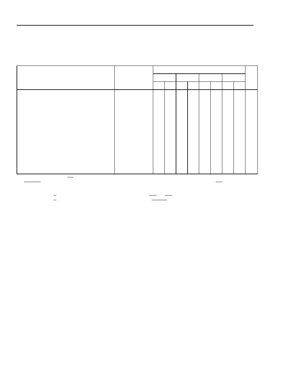
116
Lucent Technologies Inc.
Data Sheet
June 1999
ORCA Series 3C and 3T FPGAs
Timing Characteristics
(continued)
Table 49. Microprocessor Interface (MP I) Timing Characteristics (continued)
OR3Cxx Commercial: V
DD
= 5.0 V ± 5%, 0 ∞C
<
T
A
<
70 ∞C; Industrial: V
DD
= 5.0 V ± 10%, ≠40 ∞C
<
T
A
<
+85 ∞C.
OR3Txxx Commercial: V
DD
= 3.0 V to 3.6 V, 0 ∞C
<
T
A
<
70 ∞C; Industrial: V
DD
= 3.0 V to 3.6 V, ≠40 ∞C
<
T
A
<
+85
∞C.
1. For user system flexibility,
CS0
and CS1 may be set up to any one of the three rising clock edges, beginning with the rising clock edge when
MPI_STRB
is low. If both chip selects are valid and the setup time is met, the MPI will latch the chip select state, and
CS0
and CS1 may go
inactive before the end of the read/write cycle.
2. 0.5 MPI_CLK.
3. Write data and W/R have to be valid starting from the clock cycle after both ADS and CS0 and CS1 are recognized.
4. Write data and W/R have to be held until the microprocessor receives a valid RDYRCV.
5. User Logic Delay has no predefined value. The user must generate a UEND signal to complete the cycle.
6. USTART_DEL is based on the falling clock edge.
7. There is no specific time associated with this delay. The user must assert UEND low to complete this cycle.
8. The user must assert interrupt request low until a service routine is executed.
9. This should be at least one MPI_CLK cycle.
10. User should set up read data so that RDS_SET and RDS_HLD can be met for the microprocessor timing.
Notes:
Read and write descriptions are referenced to the host microprocessor; e.g., a read is a read by the host (
PowerPC
,
i960
) from the FPGA.
PowerPC
and
i960
timings to/from the clock are relative to the clock at the FPGA microprocessor interface clock pin (MPI_CLK).
Parameter
Symbol
Speed
Unit
≠4
≠5
≠6
≠7
Min Max Min Max Min Max Min Max
User Logic Delay
(5)
User Logic Delay
--
--
--
--
--
--
--
--
ns
User Start Delay (MPI_CLK falling to USTART)
(6)
USTART_DEL
--
3.6
--
3.4
--
3.3
--
2.8
ns
User Start Clear Delay (MPI_CLK to USTART)
USTARTCLR_DEL
--
7.5
--
7.3
--
7.1
--
6.0
ns
User End Delay (USTART low to UEND low)
(7)
UEND_DEL
--
--
--
--
--
--
--
--
ns
Synchronous User Timing:
User End Setup (UEND to MPI_CLK)
UEND_SET
0.00
--
0.00
--
0.00
--
0.00
--
ns
User End Hold (UEND to MPI_CLK)
UEND_HLD
1.0
--
0.95
--
0.88
--
0.75
--
ns
Data Setup for Read (D[7:0] to MPI_CLK)
(9)
RDS_SET
--
--
--
--
--
--
--
--
ns
Data Hold for Read (D[7:0] from MPI_CLK)
(9)
RDS_HLD
--
--
--
--
--
--
--
--
ns
Asynchronous User Timing:
User End to Read Data Delay (UEND to
D[7:0])
(10)
RDA_DEL
--
--
--
--
--
--
--
--
ns
Data Hold from User Start (low)
(9)
RDA_HLD
--
--
--
--
--
--
--
--
ns
Interrupt Request Pulse Width
(8)
TUIRQ_PW
--
--
--
--
--
--
--
--
ns
Lucent Technologies Inc.
117
Data Sheet
June 1999
ORCA Series 3C and 3T FPGAs
Timing Characteristics
(continued)
5-5832(F)
Figure 67. MPI
PowerPC
User Space Read Timing
5-5840(F)
Figure 68. MPI
PowerPC
User Space Write Timing
MPI_CLK
A[4:0]
MPI_RW (RD/WR)
CS0, CS1
D[7:0]
MPI_STRB (TS)
UA[3:0]
URDWRN
USTART
UEND
MPI_ACK (TA)
MPI_BI (BI)
A_SET
RW_SET
CS_SET
URDWR_DEL
RDS_SET
A_HLD
CS_HLD
RDS_HLD
RDA_DEL
RDA_HLD
USTART_DEL
USER LOGIC DELAY
TA_DEL
BI_DEL
BI_DEL
TA_DEL
UEND_DEL
USTARTCLR_DEL
RW_HLD
UA_DEL
UEND_SET
TA_DELZ
BI_DELZ
MPI_CLK
A[4:0]
MPI_RW (RD/WR)
CS0, CS1
D[7:0]
MPI_STRB (TS)
UA[3:0]
URDWRN
USTART
UEND
MPI_ACK (TA)
MPI_BI (BI)
A_SET
RW_SET
CS_SET
URDWR_DEL
UEND_SET
A_HLD
RW_HLD
CS_HLD
WD_HLD
USTART_DEL
USER LOGIC DELAY
TA_DEL
BI_DEL
BI_DEL
TA_DEL
UEND_DEL
USTARTCLR_DEL
UA_DEL
BI_DELZ
TA_DELZ
WD_SET
118
Lucent Technologies Inc.
Data Sheet
June 1999
ORCA Series 3C and 3T FPGAs
Timing Characteristics
(continued)
5-5832(F).c
Figure 69. MPI
PowerPC
Internal Read Timing
5-5840(F).e
Figure 70. MPI
PowerPC
Internal Write Timing
MPI_CLK
A[4:0]
MPI_RW (RD/WR)
CS0, CS1
D[7:0]
MPI_STRB (TS)
UA[3:0]
URDWRN
MPI_ACK (TA)
MPI_BI (BI)
A_SET
RW_SET
CS_SET
URDWR_DEL
RDS_SET
A_HLD
CS_HLD
RDS_HLD
RDA_DEL
RDA_HLD
TA_DEL
BI_DEL
BI_DEL
TA_DEL
RW_HLD
UA_DEL
UEND_SET
TA_DELZ
BI_DELZ
MPI_CLK
A[4:0]
MPI_RW (RD/WR)
CS0, CS1
D[7:0]
MPI_STRB (TS)
UA[3:0]
URDWRN
MPI_ACK (TA)
MPI_BI (BI)
A_SET
RW_SET
CS_SET
URDWR_DEL
A_HLD
RW_HLD
CS_HLD
WD_HLD
TA_DEL
BI_DEL
BI_DEL
TA_DEL
UA_DEL
BI_DELZ
TA_DELZ
WD_SET
Lucent Technologies Inc.
119
Data Sheet
June 1999
ORCA Series 3C and 3T FPGAs
Timing Characteristics
(continued)
5-5831(F).b
Figure 71. MPI
i960
User Space Read Timing
5-5830(F).b
Figure 72. MPI
i960
User Space Write Timing
MPI_CLK
D[7:0]
MPI_RW (W/R)
CS0, CS1
MPI_ALE (ALE)
MPI_STRB (ADS)
UA[3:0]
URDWRN
USTART
UEND
MPI_ACK (RDYRCV)
ADSN_HLD
A_SET
ADDR
DATA
UA_DEL
UEND_SET
RDYRCV_DEL
USTART_DEL
USER LOGIC DELAY
RDYRCV_DEL
UEND_DEL
USTARTCLR_DEL
CS_HLD
RDS_HLD
RW_HLD
RDS_SET
RDA_DEL
RDA_HLD
BE0, BE1
BE_HLD
BE_SET
RDYRCV_DELZ
URDWR_DEL
ADSN_SET
RW_SET
A_HLD
CS_SET
MPI_CLK
D[7:0]
MPI_RW (W/R)
CS0, CS1
MPI_ALE (ALE)
MPI_STRB (ADS)
UA[3:0]
URDWRN
USTART
UEND
MPI_ACK (RDYRCV)
A_HLD
ADSN_HLD
A_SET
DATA
URDWR_DEL
UEND_SET
RDYRCV_DEL
USTART_DEL
USER LOGIC DELAY
RDYRCV_DEL
UEND_DEL
USTARTCLR_DEL
CS_HLD
WD_HLD
RW_HLD
WD_SET
UA_DEL
RDYRCV_DELZ
ADDR
CS_SET
RW_SET
ADSN_SET
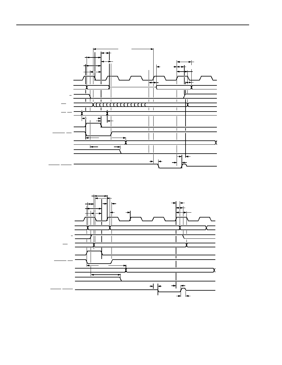
120
Lucent Technologies Inc.
Data Sheet
June 1999
ORCA Series 3C and 3T FPGAs
Timing Characteristics
(continued)
5-5831(F).c
Figure 73. MPI
i960
Internal Read Timing
5-5830(F).c
Figure 74. MPI
i960
Internal Write Timing
MPI_CLK
D[7:0]
MPI_RW (W/R)
CS0, CS1
MPI_ALE (ALE)
MPI_STRB (ADS)
UA[3:0]
URDWRN
MPI_ACK (RDYRCV)
ADSN_HLD
A_SET
ADDR
DATA
UA_DEL
RDYRCV_DEL
RDYRCV_DEL
CS_HLD
RDS_HLD
RW_HLD
RDS_SET
RDA_DEL
RDA_HLD
BE0, BE1
BE_HLD
BE_SET
RDYRCV_DELZ
URDWR_DEL
ADSN_SET
RW_SET
A_HLD
CS_SET
MPI_CLK
D[7:0]
MPI_RW (W/R)
CS0, CS1
MPI_ALE (ALE)
MPI_STRB (ADS)
UA[3:0]
URDWRN
MPI_ACK (RDYRCV)
A_HLD
ADSN_HLD
A_SET
DATA
URDWR_DEL
RDYRCV_DEL
RDYRCV_DEL
CS_HLD
WD_HLD
RW_HLD
WD_SET
UA_DEL
RDYRCV_DELZ
ADDR
CS_SET
RW_SET
ADSN_SET
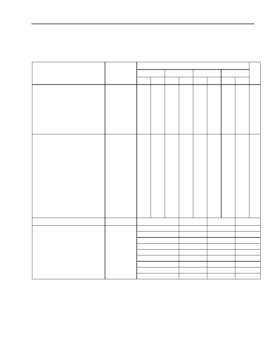
Lucent Technologies Inc.
121
Data Sheet
June 1999
ORCA Series 3C and 3T FPGAs
Timing Characteristics
(continued)
Table 50. Programmable Clock Manager (PCM) Timing Characteristics (Preliminary Information)
OR3Cxx Commercial: V
DD
= 5.0 V ± 5%, 0 ∞C
T
A
<
70 ∞C; Industrial: V
DD
= 5.0 V ± 10%, ≠40 ∞C
<
T
A
<
+85 ∞C.
OR3Txxx Commercial: V
DD
= 3.0 V to 3.6 V, 0 ∞C
<
T
A
<
70 ∞C; Industrial: V
DD
= 3.0 V to 3.6 V, ≠40 ∞C
<
T
A
<
+85 ∞C.
* Input frequency tolerance is the allowed input clock frequency change in parts per million.
See Table 29 and Table 30 for acquisition times for individual frequencies.
PLL mode, divider reg = 1111111 (input freq. = output freq.).
Note: All timing values for the PCM are preliminary information.
Parameter
Symbol
Speed
Unit
-4
-5
-6
-7
Min
Max
Min
Max
Min
Max
Min
Max
Input Clock Frequency:
FPCMI
OR3Cxx
5
133
5
133
--
--
--
--
MHz
OR3Txxx
--
--
5
133
5
133
5
133
MHz
Output Clock Frequency:
FPCMO
OR3Cxx
5
135
5
135
--
--
--
--
MHz
OR3Txxx
--
--
5
100
5
100
5
100
MHz
Input Clock Duty Cycle
PCMI_DUTY
30.00
70.00
30.00
70.00
30.00
70.00
30.00
70.00
%
Output Clock Duty Cycle
PCMO_DUTY
3.13
96.90
3.13
96.90
3.13
96.90
3.13
96.90
%
Input Frequency Tolerance*
FTOL
--
26400
--
26400
--
26400
--
26400 ppm
PCM Acquisition Time (CLK In to
LOCK)
PCM_ACQ
36
100
36
100
36
100
36
100
µs
PCM Off Delay (config. Done-L, WE to
PCM power off)
PCMOFF_DEL
--
100.0
--
100.0
--
100.0
--
100.0
ns
PCM Delay in DLL Mode (propagation
delay)
PCMDLL-DEL
--
1.95
--
1.82
--
1.63
--
1.50
ns
PCM Delay in PLL Mode (propagation
delay)
PCMPLL_DEL
--
0.00
--
0.00
--
0.00
--
0.00
ns
PCM Clock In to PCM Clock Out
(CLK In to ECLK)
PCMBYE_DEL
--
0.47
--
0.36
--
0.26
--
0.24
ns
PCM Clock In to PCM Clock Out
(CLK In to SCLK)
PCMBYS_DEL
--
0.47
--
0.36
--
0.26
--
0.24
ns
Routed Clock-in Delay (routing to PCM
phase detect, using DIV0)
RTCKD_DEL
--
1.30
--
1.10
--
0.90
--
TBD
ns
System Clock-out Delay (PCM oscilla-
tor to SCLK output at PCM)
PCMSCK_DEL
--
2.70
--
2.20
--
1.90
--
TBD
ns
Parameter
Symbol
f
OUT
(MHz)
PLL Mode
DLL Mode
Unit
Output Jitter
OUTJIT
5--20
250
200
ps
21--30
210
170
ps
31--40
180
145
ps
41--50
155
123
ps
51--60
130
105
ps
61--70
110
90
ps
71--80
95
75
ps
81--90
80
65
ps
91--100
70
55
ps
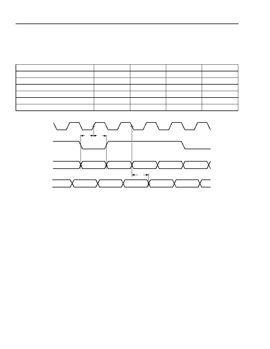
122
Lucent Technologies Inc.
Data Sheet
June 1999
ORCA Series 3C and 3T FPGAs
Timing Characteristics
(continued)
Table 51. Boundary-Scan Timing Characteristics
OR3Cxx Commercial: V
DD
= 5.0 V ± 5%, 0 ∞C
<
T
A
<
70 ∞C; Industrial: V
DD
= 5.0 V ± 10%, ≠40 ∞C
<
T
A
<
+85 ∞C.
OR3Txxx Commercial: V
DD
= 3.0 V to 3.6 V, 0 ∞C
<
T
A
<
70 ∞C; Industrial: V
DD
= 3.0 V to 3.6 V, ≠40 ∞C
<
T
A
<
+85
∞C.
5-6764(F)
Figure 75. Boundary-Scan Timing Diagram
Parameter
Symbol
Min
Max
Unit
TDI/TMS to TCK Setup Time
T
S
25.0
--
ns
TDI/TMS Hold Time from TCK
T
H
0.0
--
ns
TCK Low Time
T
CL
50.0
--
ns
TCK High Time
T
CH
50.0
--
ns
TCK to TDO Delay
T
D
--
20.0
ns
TCK Frequency
T
TCK
--
10.0
MHz
TCK
TMS
TDI
TDO
T
S
T
H
T
D

Lucent Technologies Inc.
123
Data Sheet
June 1999
ORCA Series 3C and 3T FPGAs
Timing Characteristics
(continued)
Clock Timing
Table 52. ExpressCLK (ECLK) and Fast Clock (FCLK) Timing Characteristics
OR3Cxx Commercial: V
DD
= 5.0 V ± 5%, 0 ∞C
<
T
A
<
70 ∞C; Industrial: V
DD
= 5.0 V ± 10%, ≠40 ∞C
<
T
A
<
+85 ∞C.
OR3Txxx Commercial: V
DD
= 3.0 V to 3.6 V, 0 ∞C
<
T
A
<
70 ∞C; Industrial: V
DD
= 3.0 V to 3.6 V, ≠40 ∞C
<
T
A
<
+85 ∞C.
Notes:
The ECLK delays are to all of the PICs on one side of the device for middle pin input, or two sides of the device for corner pin input. The delay
includes both the input buffer delay and the clock routing to the PIC clock input.
The FCLK delays are for a fully routed clock tree that uses the ExpressCLK input into the fast clock network. It includes both the input buffer
delay and the clock routing to the PFU CLK input. The delay will be reduced if any of the clock branches are not used.
Device
(T
J
= 85 ∞C, V
DD
= min)
Symbol
Speed
Unit
-4
-5
-6
-7
Min
Max
Min
Max
Min
Max
Min
Max
Clock Control Timing Delay Through
CLKCNTRL (input from corner)
ECLKC_DEL
0.31
--
0.31
--
0.31
--
0.31
--
ns
Delay Through CLKCNTRL (input from inter-
nal clock controller PAD)
ECLKM_DEL
1.54
--
1.17
--
1.00
--
0.92
--
ns
Clock Shutoff Timing:
Setup from Middle ECLK (shut off to CLK)
Hold from Middle ECLK (shut off from CLK)
Setup from Corner ECLK (shut off to CLK)
Hold from Corner ECLK (shut off from CLK)
OFFM_SET
OFFM_HLD
OFFC_SET
OFFC_HLD
0.77
0.00
0.77
0.00
--
--
--
--
0.51
0.00
0.51
0.00
--
--
--
--
0.44
0.00
0.44
0.00
--
--
--
--
0.41
0.00
0.41
0.00
--
--
--
--
ns
ns
ns
ns
ECLK Delay (middle pad):
OR3T20
OR3T30
OR3C/T55
OR3C/T80
OR3T125
ECLKM_DEL
--
--
--
--
--
--
--
3.50
3.67
--
--
--
--
--
--
2.56
2.62
2.74
2.86
3.06
--
--
--
--
--
2.05
2.08
2.13
2.19
2.29
--
--
--
--
--
1.78
1.80
1.85
1.90
1.98
ns
ns
ns
ns
ns
ECLK Delay (corner pad):
OR3T20
OR3T30
OR3C/T55
OR3C/T80
OR3T125
ECLKC_DEL
--
--
--
--
--
--
--
5.47
5.64
--
--
--
--
--
--
4.48
4.53
4.64
4.77
4.96
--
--
--
--
--
3.85
3.97
4.22
4.47
4.85
--
--
--
--
--
3.36
3.47
3.69
3.92
4.27
ns
ns
ns
ns
ns
FCLK Delay (middle pad):
OR3T20
OR3T30
OR3C/T55
OR3C/T80
OR3T125
FCLKM_DEL
--
--
--
--
--
--
--
8.24
8.87
--
--
--
--
--
--
5.91
6.12
6.59
7.11
7.98
--
--
--
--
--
4.59
4.66
4.83
5.01
5.33
--
--
--
--
--
3.81
3.89
4.06
4.26
4.59
ns
ns
ns
ns
ns
FCLK Delay (corner pad):
OR3T20
OR3T30
OR3C/T55
OR3C/T80
OR3T125
FCLKC_DEL
--
--
--
--
--
--
--
10.34
11.01
--
--
--
--
--
--
7.88
8.11
8.60
9.15
10.07
--
--
--
--
--
6.41
6.58
6.95
7.34
7.96
--
--
--
--
--
5.40
5.58
5.94
6.33
6.94
ns
ns
ns
ns
ns
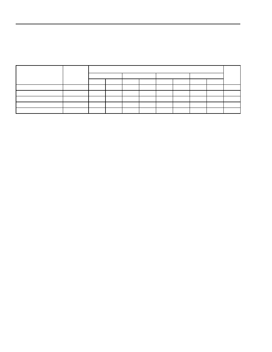
124
Lucent Technologies Inc.
Data Sheet
June 1999
ORCA Series 3C and 3T FPGAs
Timing Characteristics
(continued)
Table 53. General-Purpose Clock Timing Characteristics (Internally Generated Clock)
OR3Cxx Commercial: V
DD
= 5.0 V ± 5%, 0 ∞C
<
T
A
<
70 ∞C; Industrial: V
DD
= 5.0 V ± 10%, ≠40 ∞C
<
T
A
<
+85 ∞C.
OR3Txxx Commercial: V
DD
= 3.0 V to 3.6 V, 0 ∞C
<
T
A
<
70 ∞C; Industrial: V
DD
= 3.0 V to 3.6 V, ≠40 ∞C
<
T
A
<
+85 ∞C.
Notes:
This table represents the delay for an internally generated clock from the clock tree input in one of the four middle PICs (using pSW routing) on
any side of the device which is then distributed to the PFU/PIO clock inputs. If the clock tree input used is located at any other PIC, see the
results reported by
ORCA
Foundry.
This clock delay is for a fully routed clock tree that uses the general clock network. The delay will be reduced if any of the clock branches are not
used. See pin-to-pin timing in Table 56 for clock delays of clocks input on general I/O pins.
Device
(T
J
= 85 ∞C, V
DD
= min)
Symbol
Speed
Unit
-4
-5
-6
-7
Min
Max
Min
Max
Min
Max
Min
Max
OR3T20
CLK_DEL
--
--
--
4.22
--
3.46
--
2.84
ns
OR3T30
CLK_DEL
--
--
--
4.29
--
3.48
--
2.87
ns
OR3C/T55
CLK_DEL
--
5.34
--
4.41
--
3.53
--
2.93
ns
OR3C/T80
CLK_DEL
--
5.49
--
4.52
--
3.57
--
2.98
ns
OR3T125
CLK_DEL
--
--
--
4.80
--
3.71
--
3.13
ns
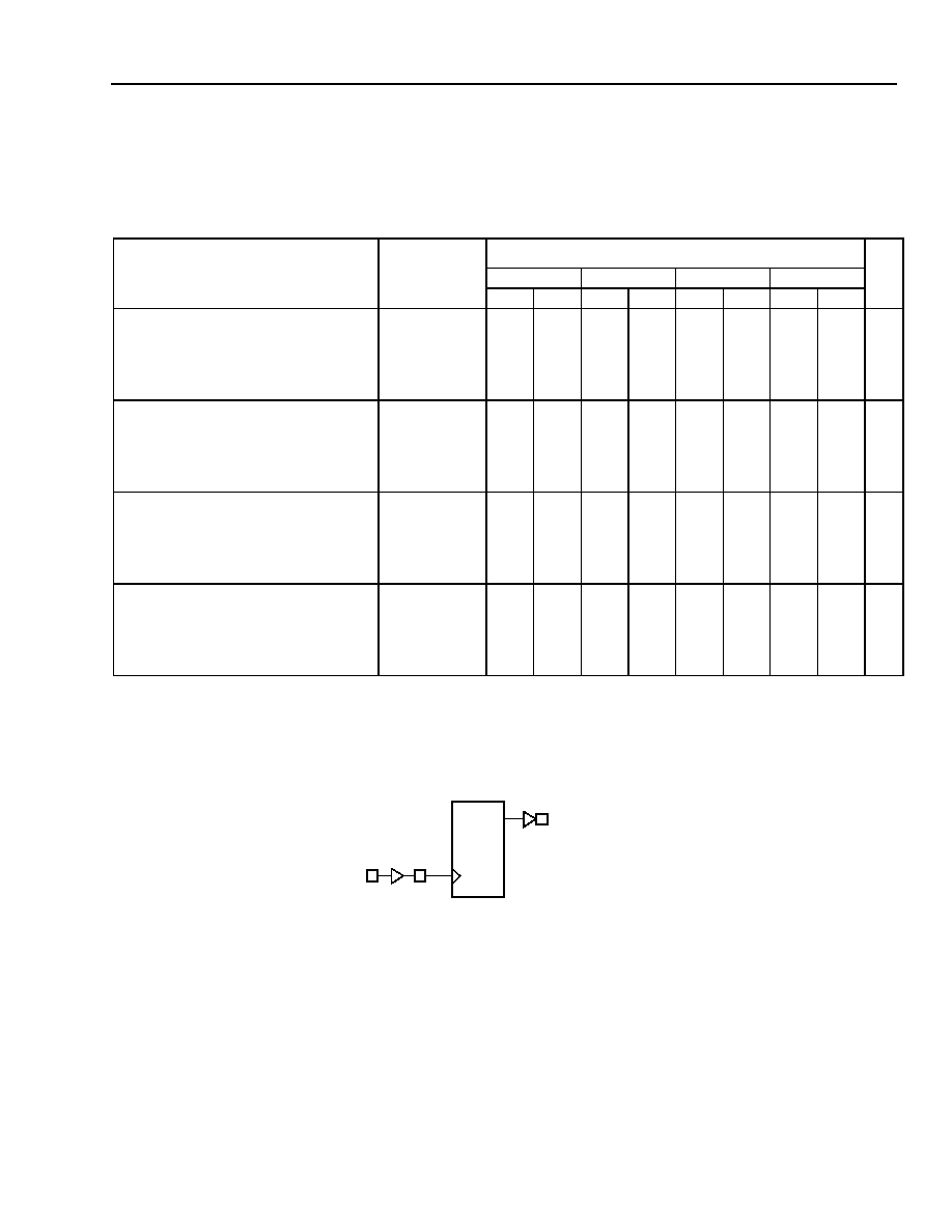
Lucent Technologies Inc.
125
Data Sheet
June 1999
ORCA Series 3C and 3T FPGAs
Timing Characteristics
(continued)
Table 54. OR3Cxx ExpressCLK to Output Delay (Pin-to-Pin)
OR3Cxx Commercial: V
DD
= 5.0 V ± 5%, 0 ∞C
<
T
A
<
70 ∞C; Industrial: V
DD
= 5.0 V ± 10%, ≠40 ∞C
<
T
A
<
+85 ∞C; C
L
= 50 pF.
OR3Txxx Commercial: V
DD
= 3.0 V to 3.6 V, 0 ∞C
<
T
A
<
70 ∞C; Industrial: V
DD
= 3.0 V to 3.6 V, ≠40 ∞C
<
T
A
<
+85 ∞C;C
L
=
50 pF.
Notes:
Timing is without the use of the programmable clock manager (PCM).
This clock delay is for a fully routed clock tree that uses the ExpressCLK network. It includes both the input buffer delay, the clock routing to the
PIO CLK input, the clock
Q of the FF, and the delay through the output buffer. The given timing requires that the input clock pin be located at
one of the six ExpressCLK inputs of the device, and that a PIO FF be used.
5-4846(F).a
Figure 76. ExpressCLK to Output Delay
Description
(T
J
= 85 ∞C, V
DD
= min)
Device
Speed
Unit
-4
-5
-6
-7
Min
Max
Min
Max
Min
Max
Min
Max
ECLK Middle Input Pin
OUTPUT Pin
(Fast)
OR3T20
OR3T30
OR3C/T55
OR3C/T80
OR3T125
--
--
--
--
--
--
--
9.93
10.10
--
--
--
--
--
--
7.78
7.84
7.96
8.08
8.28
--
--
--
--
--
5.40
5.43
5.48
5.54
5.64
--
--
--
--
--
4.38
4.40
4.44
4.49
4.58
ns
ns
ns
ns
ns
ECLK Middle Input Pin
OUTPUT Pin
(Slewlim)
OR3T20
OR3T30
OR3C/T55
OR3C/T80
OR3T125
--
--
--
--
--
--
--
12.37
12.54
--
--
--
--
--
--
9.77
9.83
9.95
10.07
10.27
--
--
--
--
--
6.07
6.10
6.15
6.21
6.31
--
--
--
--
--
4.91
4.93
4.97
5.02
5.11
ns
ns
ns
ns
ns
ECLK Middle Input Pin
OUTPUT Pin
(Sinklim)
OR3T20
OR3T30
OR3C/T55
OR3C/T80
OR3T125
--
--
--
--
--
--
--
13.73
13.90
--
--
--
--
--
--
11.12
11.18
11.30
11.42
11.62
--
--
--
--
--
10.92
10.95
11.00
11.06
11.16
--
--
--
--
--
9.65
9.67
9.71
9.76
9.85
ns
ns
ns
ns
ns
Additional Delay if ECLK Corner Pin Used
OR3T20
OR3T30
OR3C/T55
OR3C/T80
OR3T125
--
--
--
--
--
--
--
1.97
1.97
--
--
--
--
--
--
1.91
1.91
1.91
1.91
1.90
--
--
--
--
--
1.80
1.90
2.09
2.28
2.57
--
--
--
--
--
1.58
1.67
1.84
2.02
2.29
ns
ns
ns
ns
ns
OUTPUT (50 pF LOAD)
Q
D
ECLK
ECLK
PIO FF
CLKCNTRL
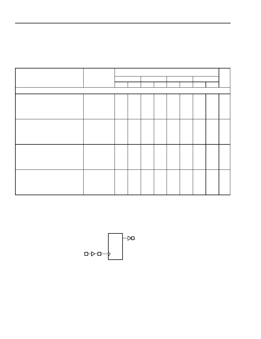
126
Lucent Technologies Inc.
Data Sheet
June 1999
ORCA Series 3C and 3T FPGAs
Timing Characteristics
(continued)
Table 55. OR3Cxx Fast Clock (FCLK) to Output Delay (Pin-to-Pin)
OR3Cxx Commercial: V
DD
= 5.0 V ± 5%, 0 ∞C
<
T
A
<
70 ∞C; Industrial: V
DD
= 5.0 V ± 10%, ≠40 ∞C
<
T
A
<
+85 ∞C; C
L
= 50 pF.
OR3Txxx Commercial: V
DD
= 3.0 V to 3.6 V, 0 ∞C
<
T
A
<
70 ∞C; Industrial: V
DD
= 3.0 V to 3.6 V, ≠40 ∞C
<
T
A
<
+85 ∞C;
C
L =
50 pF.
Notes:
Timing is without the use of the programmable clock manager (PCM).
This clock delay is for a fully routed clock tree that uses the primary clock network. It includes both the input buffer delay, the clock routing to the
PIO CLK input, the clock
Q of the FF, and the delay through the output buffer. The delay will be reduced if any of the clock branches are not
used. The given timing requires that the input clock pin be located at one of the six ExpressCLK inputs of the device and that a PIO FF be used.
5-4846(F).b
Figure 77. Fast Clock to Output Delay
Description
(T
J
= 85 ∞C, V
DD
= min)
Device
Speed
Unit
-4
-5
-6
-7
Min
Max
Min
Max
Min
Max
Min
Max
Output Not on Same Side of Device As Input Clock (Fast Clock Delays Using ExpressCLK Inputs)
ECLK Middle Input Pin
OUTPUT Pin
(Fast)
OR3T20
OR3T30
OR3C/T55
OR3C/T80
OR3T125
--
--
--
--
--
--
--
14.68
15.30
--
--
--
--
--
--
11.13
11.35
11.81
12.33
13.20
--
--
--
--
--
7.94
8.01
8.18
8.36
8.68
--
--
--
--
--
6.40
6.48
6.66
6.85
7.19
ns
ns
ns
ns
ns
ECLK Middle Input Pin
OUTPUT Pin
(Slewlim)
OR3T20
OR3T30
OR3C/T55
OR3C/T80
OR3T125
--
--
--
--
--
--
--
17.11
17.74
--
--
--
--
--
--
13.12
13.33
13.80
14.32
15.19
--
--
--
--
--
8.61
8.68
8.85
9.04
9.35
--
--
--
--
--
6.93
7.01
7.19
7.38
7.72
ns
ns
ns
ns
ns
ECLK Middle Input Pin
OUTPUT Pin
(Sinklim)
OR3T20
OR3T30
OR3C/T55
OR3C/T80
OR3T125
--
--
--
--
--
--
--
18.47
19.10
--
--
--
--
--
--
14.47
14.68
15.15
15.67
16.54
--
--
--
--
--
13.46
13.53
13.70
13.88
14.20
--
--
--
--
--
11.67
11.75
11.93
12.12
12.46
ns
ns
ns
ns
ns
Additional Delay if ECLK Corner Pin
Used
OR3T20
OR3T30
OR3C/T55
OR3C/T80
OR3T125
--
--
--
--
--
--
--
2.10
2.14
--
--
--
--
--
--
1.97
1.99
2.01
2.04
2.09
--
--
--
--
--
1.82
1.92
2.12
2.33
2.63
--
--
--
--
--
1.60
1.69
1.88
2.07
2.39
ns
ns
ns
ns
ns
OUTPUT (50 pF LOAD)
Q
D
ECLK
FCLK
PIO FF
CLKCNTRL
Lucent Technologies Inc.
127
Data Sheet
June 1999
ORCA Series 3C and 3T FPGAs
Timing Characteristics
(continued)
Table 56. OR3Cxx General System Clock (SCLK) to Output Delay (Pin-to-Pin)
OR3Cxx Commercial: V
DD
= 5.0 V ± 5%, 0 ∞C
<
T
A
<
70 ∞C; Industrial: V
DD
= 5.0 V ± 10%, ≠40 ∞C
<
T
A
<
+85 ∞C; C
L
= 50 pF.
OR3Txxx Commercial: V
DD
= 3.0 V to 3.6 V, 0 ∞C
<
T
A
<
70 ∞C; Industrial: V
DD
= 3.0 V to 3.6 V, ≠40 ∞C
<
T
A
<
+85 ∞C;
C
L
=
50 pF.
Note:
This clock delay is for a fully routed clock tree that uses the primary clock network. It includes both the input buffer delay, the clock routing to the
PIO CLK input, the clock
Q of the FF, and the delay through the output buffer. The delay will be reduced if any of the clock branches are not
used. The given timing requires that the input clock pin be located at one of the four center PICs on any side of the device and that a PIO FF be
used. For clock pins located at any other PIO, see the results reported by
ORCA
Foundry.
5-4846(F)
Figure 78. System Clock to Output Delay
Description
(T
J
= 85 ∞C, V
DD
= min)
Device
Speed
Unit
-4
-5
-6
-7
Min
Max
Min
Max
Min
Max
Min
Max
Output On Same Side of Device As Input Clock (System Clock Delays Using General User I/O Inputs)
Clock Input Pin (mid-PIC)
OUTPUT Pin (Fast)
OR3T20
OR3T30
OR3C/T55
OR3C/T80
OR3T125
--
--
--
--
--
--
--
14.91
15.71
--
--
--
--
--
--
11.35
11.63
12.17
12.80
13.69
--
--
--
--
--
7.74
7.93
8.28
8.66
9.24
--
--
--
--
--
6.10
6.27
6.59
6.95
7.49
ns
ns
ns
ns
ns
Clock Input Pin (mid-PIC)
OUTPUT Pin
(Slewlim)
OR3T20
OR3T30
OR3C/T55
OR3C/T80
OR3T125
--
--
--
--
--
--
--
17.34
18.14
--
--
--
--
--
--
13.34
13.62
14.16
14.79
15.68
--
--
--
--
--
8.42
8.60
8.95
9.34
9.91
--
--
--
--
--
6.63
6.80
7.12
7.48
8.02
ns
ns
ns
ns
ns
Clock Input Pin (mid-PIC)
OUTPUT Pin
(Sinklim)
OR3T20
OR3T30
OR3C/T55
OR3C/T80
OR3T125
--
--
--
--
--
--
--
18.70
19.51
--
--
--
--
--
--
14.69
14.97
15.51
16.14
17.03
--
--
--
--
--
13.26
13.45
13.80
14.18
14.76
--
--
--
--
--
11.37
11.54
11.86
12.22
12.76
ns
ns
ns
ns
ns
Additional Delay if Non-mid-PIC Used as Clock
Pin
OR3T20
OR3T30
OR3C/T55
OR3C/T80
OR3T125
--
--
--
--
--
--
--
0.41
0.63
--
--
--
--
--
--
0.16
0.20
0.36
0.55
1.11
--
--
--
--
--
0.18
0.21
0.37
0.57
1.05
--
--
--
--
--
0.17
0.20
0.35
0.55
1.02
ns
ns
ns
ns
ns
Output Not on Same Side of Device As Input Clock (System Clock Delays Using General User I/O Inputs)
Additional Delay if Output Not on Same Side as
Input Clock Pin
OR3T20
OR3T30
OR3C/T55
OR3C/T80
OR3T125
--
--
--
--
--
--
--
0.41
0.63
--
--
--
--
--
--
0.16
0.20
0.36
0.55
1.11
--
--
--
--
--
0.18
0.21
0.37
0.57
1.05
--
--
--
--
--
0.17
0.20
0.35
0.55
1.02
ns
ns
ns
ns
ns
OUTPUT (50 pF LOAD)
Q
D
SCLK
PIO FF

128
Lucent Technologies Inc.
Data Sheet
June 1999
ORCA Series 3C and 3T FPGAs
Timing Characteristics
(continued)
Table 57. OR3C/Txxx Input to ExpressCLK (ECLK) Fast-Capture Setup/Hold Time (Pin-to-Pin)
OR3Cxx Commercial: V
DD
= 5.0 V ± 5%, 0 ∞C
<
T
A
<
70 ∞C; Industrial: V
DD
= 5.0 V ± 10%, ≠40 ∞C
<
T
A
<
+85 ∞C.
OR3Txxx Commercial: V
DD
= 3.0 V to 3.6 V, 0 ∞C
<
T
A
<
70 ∞C; Industrial: V
DD
= 3.0 V to 3.6 V, ≠40 ∞C
<
T
A
<
+85 ∞C.
Note:
The pin-to-pin timing parameters in this table should be used instead of results reported by
ORCA
Foundry.
The ECLK delays are to all of the PIOs on one side of the device for middle pin input, or two sides of the device for corner pin input. The delay
includes both the input buffer delay and the clock routing to the PIO clock input.
Description
(T
J
= 85 ∞C, V
DD
= min)
Device
Speed
Unit
-4
-5
-6
-7
Min
Max
Min
Max
Min
Max
Min
Max
Input to ECLK Setup Time (middle
ECLK pin)
OR3T20
OR3T30
OR3C/T55
OR3C/T80
OR3T125
--
--
1.36
1.25
--
--
--
--
--
--
1.34
1.30
1.22
1.14
1.03
--
--
--
--
--
0.88
0.86
0.83
0.80
0.76
--
--
--
--
--
0.83
0.82
0.80
0.77
0.74
--
--
--
--
--
ns
ns
ns
ns
ns
Input to ECLK Setup Time (middle
ECLK pin, delayed data input)
OR3T20
OR3T30
OR3C/T55
OR3C/T80
OR3T125
--
--
6.91
6.79
--
--
--
--
--
--
6.30
6.27
6.19
6.11
6.00
--
--
--
--
--
5.32
5.30
5.27
5.24
5.20
--
--
--
--
--
5.98
5.97
5.95
5.93
5.90
--
--
--
--
--
ns
ns
ns
ns
ns
Input to ECLK Setup Time (corner
ECLK pin)
OR3T20
OR3T30
OR3C/T55
OR3C/T80
OR3T125
--
--
0.00
0.00
--
--
--
--
--
--
0.00
0.00
0.00
0.00
0.00
--
--
--
--
--
0.00
0.00
0.00
0.00
0.00
--
--
--
--
--
0.00
0.00
0.00
0.00
0.00
--
--
--
--
--
ns
ns
ns
ns
ns
Input to ECLK Setup Time (corner
ECLK pin, delayed data input)
OR3T20
OR3T30
OR3C/T55
OR3C/T80
OR3T125
--
--
4.94
4.82
--
--
--
--
--
--
4.39
4.35
4.28
4.21
4.10
--
--
--
--
--
3.51
3.40
3.18
2.98
2.63
--
--
--
--
--
4.41
4.31
4.11
3.91
3.61
--
--
--
--
--
ns
ns
ns
ns
ns
Input to ECLK Hold Time (middle
ECLK pin)
OR3T20
OR3T30
OR3C/T55
OR3C/T80
OR3T125
--
--
0.00
0.00
--
--
--
--
--
--
0.00
0.00
0.00
0.00
0.00
--
--
--
--
--
0.00
0.00
0.00
0.00
0.00
--
--
--
--
--
0.00
0.00
0.00
0.00
0.00
--
--
--
--
--
ns
ns
ns
ns
ns
Input to ECLK Hold Time (middle
ECLK pin, delayed data input)
OR3T20
OR3T30
OR3C/T55
OR3C/T80
OR3T125
--
--
0.00
0.00
--
--
--
--
--
--
0.00
0.00
0.00
0.00
0.00
--
--
--
--
--
0.00
0.00
0.00
0.00
0.00
--
--
--
--
--
0.00
0.00
0.00
0.00
0.00
--
--
--
--
--
ns
ns
ns
ns
ns
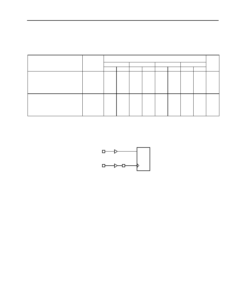
Lucent Technologies Inc.
129
Data Sheet
June 1999
ORCA Series 3C and 3T FPGAs
Timing Characteristics
(continued)
Table 57. OR3C/Txxx Input to ExpressCLK (ECLK) Fast-Capture Setup/Hold Time (Pin-to-Pin) (continued)
OR3Cxx Commercial: V
DD
= 5.0 V ± 5%, 0 ∞C
<
T
A
<
70 ∞C; Industrial: V
DD
= 5.0 V ± 10%, ≠40 ∞C
<
T
A
<
+85 ∞C.
OR3Txxx Commercial: V
DD
= 3.0 V to 3.6 V, 0 ∞C
<
T
A
<
70 ∞C; Industrial: V
DD
= 3.0 V to 3.6 V, ≠40 ∞C
<
T
A
<
+85 ∞C.
Notes:
The pin-to-pin timing parameters in this table should be used instead of results reported by
ORCA
Foundry.
The ECLK delays are to all of the PIOs on one side of the device for middle pin input, or two sides of the device for corner pin input. The delay
includes both the input buffer delay and the clock routing to the PIO clock input.
5-4847(F).b
Figure 79. Input to ExpressCLK Setup/Hold Time
Description
(T
J
= 85 ∞C, V
DD
= min)
Device
Speed
Unit
-4
-5
-6
-7
Min
Max
Min
Max
Min
Max
Min
Max
Input to ECLK Hold Time (corner
ECLK pin)
OR3T20
OR3T30
OR3C/T55
OR3C/T80
OR3T125
--
--
0.00
0.00
--
--
--
--
--
--
0.00
0.00
0.00
0.00
0.00
--
--
--
--
--
0.00
0.00
0.80
0.00
0.00
--
--
--
--
--
0.00
0.00
1.10
0.00
0.00
--
--
--
--
--
ns
ns
ns
ns
ns
Input to ECLK Hold Time (corner
ECLK pin, delayed data input)
OR3T20
OR3T30
OR3C/T55
OR3C/T80
OR3T125
--
--
0.00
0.00
--
--
--
--
--
--
0.00
0.00
0.00
0.00
0.00
--
--
--
--
--
0.00
0.00
0.00
0.00
0.00
--
--
--
--
--
0.00
0.00
0.00
0.00
0.00
--
--
--
--
--
ns
ns
ns
ns
ns
Q
D
CLK
INPUT
PIO ECLK LATCH
CLKCNTRL
ECLK

130
Lucent Technologies Inc.
Data Sheet
June 1999
ORCA Series 3C and 3T FPGAs
Timing Characteristics
(continued)
Table 58. OR3C/Txxx Input to Fast Clock Setup/Hold Time (Pin-to-Pin)
OR3Cxx Commercial: V
DD
= 5.0 V ± 5%, 0 ∞C
<
T
A
<
70 ∞C; Industrial: V
DD
= 5.0 V ± 10%, ≠40 ∞C
<
T
A
<
+85 ∞C.
OR3Txxx Commercial: V
DD
= 3.0 V to 3.6 V, 0 ∞C
<
T
A
<
70 ∞C; Industrial: V
DD
= 3.0 V to 3.6 V, ≠40 ∞C
<
T
A
<
+85 ∞C.
Notes:
The pin-to-pin timing parameters in this table should be used instead of results reported by
ORCA
Foundry.
The FCLK delays are for a fully routed clock tree that uses the ExpressCLK input into the fast clock network. It includes both the input buffer
delay and the clock routing to the PFU CLK input. The delay will be reduced if any of the clock branches are not used.
Description
(T
J
= 85 ∞C, V
DD
= min)
Device
Speed
Unit
-4
-5
-6
-7
Min
Max
Min
Max
Min
Max
Min
Max
Output Not on Same Side of Device As Input Clock (Fast Clock Delays Using ExpressCLK Inputs)
Input to FCLK Setup Time (middle
ECLK pin)
OR3T20
OR3T30
OR3C/T55
OR3C/T80
OR3T125
--
--
0.00
0.00
--
--
--
--
--
--
0.00
0.00
0.00
0.00
0.00
--
--
--
--
--
0.00
0.00
0.00
0.00
0.00
--
--
--
--
--
0.00
0.00
0.00
0.00
0.00
--
--
--
--
--
ns
ns
ns
ns
ns
Input to FCLK Setup Time (middle
ECLK pin, delayed data input)
OR3T20
OR3T30
OR3C/T55
OR3C/T80
OR3T125
--
--
0.29
0.14
--
--
--
--
--
--
0.80
0.74
0.62
0.50
0.22
--
--
--
--
--
0.58
0.55
0.51
0.46
0.33
--
--
--
--
--
2.20
2.17
2.11
2.06
1.90
--
--
--
--
--
ns
ns
ns
ns
ns
Input to FCLK Setup Time (corner
ECLK pin)
OR3T20
OR3T30
OR3C/T55
OR3C/T80
OR3T125
--
--
0.00
0.00
--
--
--
--
--
--
0.00
0.00
0.00
0.00
0.00
--
--
--
--
--
0.00
0.00
0.00
0.00
0.00
--
--
--
--
--
0.00
0.00
0.00
0.00
0.00
--
--
--
--
--
ns
ns
ns
ns
ns
Input to FCLK Setup Time (corner
ECLK pin, delayed data input)
OR3T20
OR3T30
OR3C/T55
OR3C/T80
OR3T125
--
--
0.00
0.00
--
--
--
--
--
--
0.00
0.00
0.00
0.00
0.00
--
--
--
--
--
0.00
0.00
0.00
0.00
0.00
--
--
--
--
--
0.00
0.00
0.00
0.00
0.00
--
--
--
--
--
ns
ns
ns
ns
ns
Input to FCLK Hold Time (middle
ECLK pin)
OR3T20
OR3T30
OR3C/T55
OR3C/T80
OR3T125
--
--
6.33
6.95
--
--
--
--
--
--
4.29
4.50
4.97
5.49
6.36
--
--
--
--
--
3.72
3.80
3.96
4.15
4.47
--
--
--
--
--
3.27
3.35
3.52
3.72
4.05
--
--
--
--
--
ns
ns
ns
ns
ns
Lucent Technologies Inc.
131
Data Sheet
June 1999
ORCA Series 3C and 3T FPGAs
Timing Characteristics
(continued)
Table 58. OR3C/Txxx Input to Fast Clock Setup/Hold Time (Pin-to-Pin) (continued)
OR3Cxx Commercial: V
DD
= 5.0 V ± 5%, 0 ∞C
<
T
A
<
70 ∞C; Industrial: V
DD
= 5.0 V ± 10%, ≠40 ∞C
<
T
A
<
+85 ∞C.
OR3Txxx Commercial: V
DD
= 3.0 V to 3.6 V, 0 ∞C
<
T
A
<
70 ∞C; Industrial: V
DD
= 3.0 V to 3.6 V, ≠40 ∞C
<
T
A
<
+85 ∞C.
Notes:
The pin-to-pin timing parameters in this table should be used instead of results reported by
ORCA
Foundry.
The FCLK delays are for a fully routed clock tree that uses the ExpressCLK input into the fast clock network. It includes both the input buffer
delay and the clock routing to the PFU CLK input. The delay will be reduced if any of the clock branches are not used.
5-4847(F).a
Figure 80. Input to Fast Clock Setup/Hold Time
Description
(T
J
= 85 ∞C, V
DD
= min)
Device
Speed
Unit
-4
-5
-6
-7
Min
Max
Min
Max
Min
Max
Min
Max
Input to FCLK Hold Time (middle
ECLK pin, delayed data input)
OR3T20
OR3T30
OR3C/T55
OR3C/T80
OR3T125
--
--
0.00
0.00
--
--
--
--
--
--
0.00
0.00
0.00
0.00
0.00
--
--
--
--
--
0.00
0.00
0.00
0.00
0.00
--
--
--
--
--
0.00
0.00
0.00
0.00
0.00
--
--
--
--
--
ns
ns
ns
ns
ns
Input to FCLK Hold Time (corner
ECLK pin)
OR3T20
OR3T30
OR3C/T55
OR3C/T80
OR3T125
--
--
8.43
9.09
--
--
--
--
--
--
6.26
6.49
6.98
7.53
8.45
--
--
--
--
--
5.54
5.72
6.09
6.47
7.10
--
--
--
--
--
4.88
5.04
5.40
5.79
6.40
--
--
--
--
--
ns
ns
ns
ns
ns
Input to FCLK Hold Time (corner
ECLK pin, delayed data input)
OR3T20
OR3T30
OR3C/T55
OR3C/T80
OR3T125
--
--
0.00
0.00
--
--
--
--
--
--
0.00
0.00
0.00
0.00
0.00
--
--
--
--
--
0.00
0.00
0.00
0.00
0.00
--
--
--
--
--
0.00
0.00
0.00
0.00
0.00
--
--
--
--
--
ns
ns
ns
ns
ns
Q
D
ECLK
INPUT
PIO FF
CLKCNTRL
FCLK
132
Lucent Technologies Inc.
Data Sheet
June 1999
ORCA Series 3C and 3T FPGAs
Timing Characteristics
(continued)
Table 59. OR3C/Txxx Input to General System Clock (SCLK) Setup/Hold Time (Pin-to-Pin)
OR3Cxx Commercial: V
DD
= 5.0 V ± 5%, 0 ∞C
<
T
A
<
70 ∞C; Industrial: V
DD
= 5.0 V ± 10%, ≠40 ∞C
<
T
A
<
+85 ∞C.
OR3Txxx Commercial: V
DD
= 3.0 V to 3.6 V, 0 ∞C
<
T
A
<
70 ∞C; Industrial: V
DD
= 3.0 V to 3.6 V, ≠40 ∞C
<
T
A
<
+85 ∞C.
Notes:
The pin-to-pin timing parameters in this table should be used instead of results reported by
ORCA
Foundry.
This clock delay is for a fully routed clock tree that uses the clock network. It includes both the input buffer delay and the clock routing to the PIO
FF CLK input. The delay will be reduced if any of the clock branches are not used. The given setup (delayed and no delay) and hold (delayed)
timing allows the input clock pin to be located in any PIO on any side of the device, but a PIO FF must be used. The hold (no delay) timing
assumes the clock pin is located at one of the four middle PICs on any side of the device and that a PIO FF is used. If the clock pin is located
elsewhere, then the last parameter in the table must be added to the hold (no delay) timing.
5-4847(F)
Figure 81. Input to System Clock Setup/Hold Time
Description
(T
J
= 85 ∞C, V
DD
= min)
Device
Speed
Unit
-4
-5
-6
-7
Min
Max
Min
Max
Min
Max
Min
Max
Input to SCLK Setup Time
OR3T20
OR3T30
OR3C/T55
OR3C/T80
OR3T125
--
--
0.00
0.00
--
--
--
--
--
--
0.00
0.00
0.00
0.00
0.00
--
--
--
--
--
0.00
0.00
0.00
0.00
0.00
--
--
--
--
--
0.00
0.00
0.00
0.00
0.00
--
--
--
--
--
ns
ns
ns
ns
ns
Input to SCLK Setup Time
(delayed data input)
OR3T20
OR3T30
OR3C/T55
OR3C/T80
OR3T125
--
--
0.99
0.79
--
--
--
--
--
--
1.33
1.22
1.09
0.93
0.78
--
--
--
--
--
1.47
1.40
1.33
1.26
1.19
--
--
--
--
--
3.09
3.03
2.97
2.91
2.86
--
--
--
--
--
ns
ns
ns
ns
ns
Input to SCLK Hold Time
OR3T20
OR3T30
OR3C/T55
OR3C/T80
OR3T125
--
--
6.82
7.62
--
--
--
--
--
--
4.74
5.01
5.56
6.19
7.07
--
--
--
--
--
3.64
3.83
4.18
4.56
5.14
--
--
--
--
--
3.04
3.22
3.54
3.89
4.44
--
--
--
--
--
ns
ns
ns
ns
ns
Input to SCLK Hold Time
(delayed data input)
OR3T20
OR3T30
OR3C/T55
OR3C/T80
OR3T125
--
--
0.00
0.00
--
--
--
--
--
--
0.00
0.00
0.00
0.00
0.00
--
--
--
--
--
0.00
0.00
0.00
0.00
0.00
--
--
--
--
--
0.00
0.00
0.00
0.00
0.00
--
--
--
--
--
ns
ns
ns
ns
ns
Additional Hold Time if Non-
mid-PIC Used as SCLK Pin
(no delay on data input)
OR3T20
OR3T30
OR3C/T55
OR3C/T80
OR3T125
--
--
0.41
0.63
--
--
--
--
--
--
0.16
0.20
0.36
0.55
1.11
--
--
--
--
--
0.18
0.21
0.37
0.57
1.05
--
--
--
--
--
0.17
0.20
0.35
0.55
1.02
--
--
--
--
--
ns
ns
ns
ns
ns
Q
D
SCLK
INPUT
PIO FF
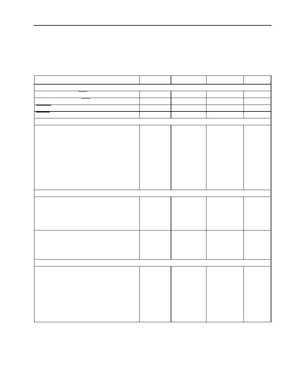
Lucent Technologies Inc.
133
Data Sheet
June 1999
ORCA Series 3C and 3T FPGAs
Timing Characteristics
(continued)
Configuration Timing
Table 60. General Configuration Mode Timing Characteristics
OR3Cxx Commercial: V
DD
= 5.0 V ± 5%, 0 ∞C
<
T
A
<
70 ∞C; Industrial: V
DD
= 5.0 V ± 10%, ≠40 ∞C
<
T
A
<
+85 ∞C.
OR3Txxx Commercial: V
DD
= 3.0 V to 3.6 V, 0 ∞C
<
T
A
<
70 ∞C; Industrial: V
DD
= 3.0 V to 3.6 V, ≠40 ∞C
<
T
A
<
+85
∞C.
* Not applicable to asynchronous peripheral mode.
Parameter
Symbol
Min
Max
Unit
All Configuration Modes
M[3:0] Setup Time to INIT High
TSMODE
0.00
--
ns
M[3:0] Hold Time from INIT High
THMODE
600.00
--
ns
RESET Pulse Width Low to Start Reconfiguration
TRW
50.00
--
ns
PRGM Pulse Width Low to Start Reconfiguration
TPGW
50.00
--
ns
Master and Asynchronous Peripheral Modes
Power-on Reset Delay
CCLK Period (M3 = 0)
(M3 = 1)
Configuration Latency (autoincrement mode):
OR3T20
(M3 = 0)
(M3 = 1)
OR3T30
(M3 = 0)
(M3 = 1)
OR3C/T55
(M3 = 0)
(M3 = 1)
OR3C/T80
(M3 = 0)
(M3 = 1)
OR3T125
(M3 = 0)
(M3 = 1)
TPO
TCCLK
TCL
15.70
60.00
480.00
11.50
92.10
15.10
121.00
23.20
185.00
33.70
270.00
52.30
418.00
52.40
200.00
1600.00
38.40*
307.00*
50.40*
403.30*
77.40*
619.00*
113.00*
900.00*
175.00*
1395.00*
ms
ns
ns
ms
ms
ms
ms
ms
ms
ms
ms
ms
ms
Microprocessor (MPI) Mode
Power-on Reset Delay
Configuration Latency (autoincrement mode):
OR3T20
OR3T30
OR3C/T55
OR3C/T80
OR3T125
TPO
TCL
15.70
27413
35445
53341
76317
116581
52.40
--
--
--
--
--
ms
write cycles
write cycles
write cycles
write cycles
write cycles
Partial Reconfiguration (explicit mode):
OR3T20
OR3T30
OR3C/T55
OR3C/T80
OR3T125
TPR
32
36
43
51
62
--
--
--
--
--
write cycles
write cycles
write cycles
write cycles
write cycles
Slave Serial Mode
Power-on Reset Delay
CCLK Period
OR3Cxx
OR3Txxx
Configuration Latency (autoincrement mode):
OR3T20
OR3T30
OR3C55
OR3T55
OR3C80
OR3T80
OR3T125
TPO
TCCLK
TCL
3.90
40
15
2.80
3.80
15.50
5.80
22.50
8.40
13.09
13.10
--
--
--
--
--
--
--
--
--
ms
ns
ns
ms
ms
ms
ms
ms
ms
ms

134
Lucent Technologies Inc.
Data Sheet
June 1999
ORCA Series 3C and 3T FPGAs
Timing Characteristics
(continued)
Table 60. General Configuration Mode Timing Characteristics (continued)
OR3Cxx Commercial: V
DD
= 5.0 V ± 5%, 0 ∞C
<
T
A
<
70 ∞C; Industrial: V
DD
= 5.0 V ± 10%, ≠40 ∞C
<
T
A
<
+85 ∞C.
OR3Txxx Commercial: V
DD
= 3.0 V to 3.6 V, 0 ∞C
<
T
A
<
70 ∞C; Industrial: V
DD
= 3.0 V to 3.6 V, ≠40 ∞C
<
T
A
<
+85
∞C.
Note: T
PO
is triggered when V
DD
reaches between 3.0 V to 4.0 V for the OR3Cxx and between 2.7 V and 3.0 V for the OR3Txxx.
Parameter
Symbol
Min
Max
Unit
Slave Parallel Mode
Power-on Reset Delay
CCLK Period:
OR3Cxx
OR3Txxx
Configuration Latency (normal mode):
OR3T20
OR3T30
OR3C55
OR3T55
OR3C80
OR3T80
OR3T125
T
PO
T
CCLK
T
CL
3.90
40.00
15.00
0.36
0.47
1.94
0.72
2.81
1.05
1.64
13.10
--
--
--
--
--
--
--
--
--
ms
ns
ns
ms
ms
ms
ms
ms
ms
ms
Partial Reconfiguration (explicit mode):
OR3T20
OR3T30
OR3C55
OR3T55
OR3C80
OR3T80
OR3T125
T
PR
0.48
0.54
1.72
0.65
2.04
0.77
0.93
--
--
--
--
--
--
--
µs/frame
µs/frame
µs/frame
µs/frame
µs/frame
µs/frame
µs/frame
INIT
Timing
INIT
High to CCLK Delay:
Slave Parallel
Slave Serial
Master Serial:
(M3 = 1)
(M3 = 0)
Master Parallel:
(M3 = 1)
(M3 = 0)
T
INIT_CCLK
1.00
1.00
1.00
0.50
4.80
1.00
--
--
3.40
2.00
16.20
3.60
µs
µs
µs
µs
µs
µs
Initialization Latency (
PRGM
high to
INIT
high):
OR3T20
OR3T30
OR3C/T55
OR3C/T80
OR3T125
T
IL
0.21
0.24
0.30
0.36
0.45
0.68
0.79
1.00
1.20
1.50
ms
ms
ms
ms
ms
INIT
High to
WR
, Asynchronous Peripheral
T
INIT_WR
2.00
--
µs
Lucent Technologies Inc.
135
Data Sheet
June 1999
ORCA Series 3C and 3T FPGAs
Timing Characteristics
(continued)
5-4531(F)
Figure 82. General Configuration Mode Timing Diagram
V
DD
CCLK
M[3:0]
PRGM
INIT
T
PO
+ T
IL
T
IL
T
CCLK
T
SMODE
T
HMODE
T
INIT_CLK
DONE
T
CL
T
PGW
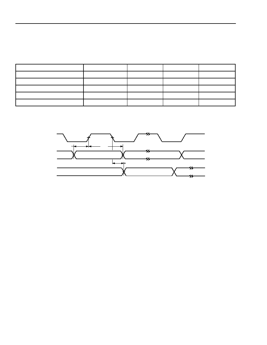
136
Lucent Technologies Inc.
Data Sheet
June 1999
ORCA Series 3C and 3T FPGAs
Timing Characteristics
(continued)
Table 61. Master Serial Configuration Mode Timing Characteristics
OR3Cxx Commercial: V
DD
= 5.0 V ± 5%, 0 ∞C
<
T
A
<
70 ∞C; Industrial: V
DD
= 5.0 V ± 10%, ≠40 ∞C
<
T
A
<
+85 ∞C.
OR3Txxx Commercial: V
DD
= 3.0 V to 3.6 V, 0 ∞C
<
T
A
<
70 ∞C; Industrial: V
DD
= 3.0 V to 3.6 V, ≠40 ∞C
<
T
A
<
+85
∞C.
* Data gets clocked out from an external serial ROM. The clock to data delay of the serial ROM must be less than the CCLK frequency since
the data available out of the serial ROM must be setup and waiting to be clocked into the FPGA before the next CCLK rising edge.
Note: Serial configuration data is transmitted out on DOUT on the falling edge of CCLK after it is input on DIN.
5-4532(F)
Figure 83. Master Serial Configuration Mode Timing Diagram
Parameter
Symbol
Min
Max
Unit
DIN Setup Time*
T
S
60.00
--
ns
DIN Hold Time
T
H
0.00
--
ns
CCLK Frequency (M3 = 0)
F
C
5.00
16.67
MHz
CCLK Frequency (M3 = 1)
F
C
0.63
2.08
MHz
CCLK to DOUT Delay
T
D
--
5.00
ns
DIN
CCLK
DOUT
T
S
T
H
BIT N
T
D
BIT N
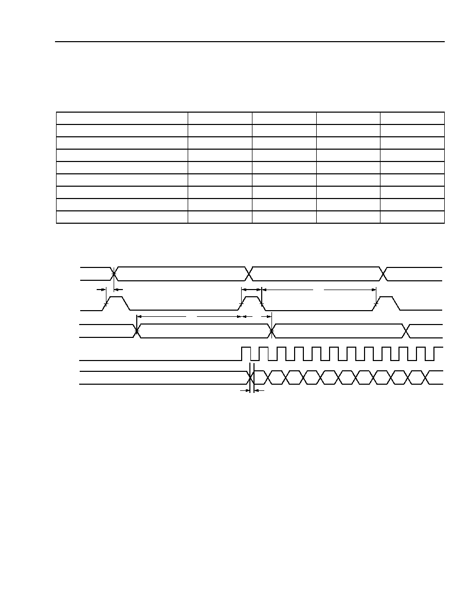
Lucent Technologies Inc.
137
Data Sheet
June 1999
ORCA Series 3C and 3T FPGAs
Timing Characteristics
(continued)
Table 62. Master Parallel Configuration Mode Timing Characteristics
OR3Cxx Commercial: V
DD
= 5.0 V ± 5%, 0 ∞C
<
T
A
<
70 ∞C; Industrial: V
DD
= 5.0 V ± 10%, ≠40 ∞C
<
T
A
<
+85 ∞C.
OR3Txxx Commercial: V
DD
= 3.0 V to 3.6 V, 0 ∞C
<
T
A
<
70 ∞C; Industrial: V
DD
= 3.0 V to 3.6 V, ≠40 ∞C
<
T
A
<
+85
∞C.
Notes:
The RCLK period consists of seven CCLKs for RCLK low and one CCLK for RCLK high.
Serial data is transmitted out on DOUT 1.5 CCLK cycles after the byte is input on D[7:0].
5-6764(F)
Figure 84. Master Parallel Configuration Mode Timing Diagram
Parameter
Symbol
Min
Max
Unit
RCLK to Address Valid
T
AV
--
60.00
ns
D[7:0] Setup Time to RCLK High
T
S
60.00
--
ns
D[7:0] Hold Time to RCLK High
T
H
0.00
--
ns
RCLK Low Time (M3 = 0)
T
CL
7.00
7.00
CCLK cycles
RCLK High Time (M3 = 0)
T
CH
1.00
1.00
CCLK cycles
RCLK Low Time (M3 = 1)
T
CL
7.00
7.00
CCLK cycles
RCLK High Time (M3 = 1)
T
CH
1.00
1.00
CCLK cycles
CCLK to DOUT
T
D
--
5.00
ns
A[17:0]
RCLK
D[7:0]
T
CL
T
CH
T
AV
CCLK
DOUT
T
H
T
S
BYTE N
BYTE N + 1
D0
D1
D2
D3
D4
D5
D6
D7
T
D
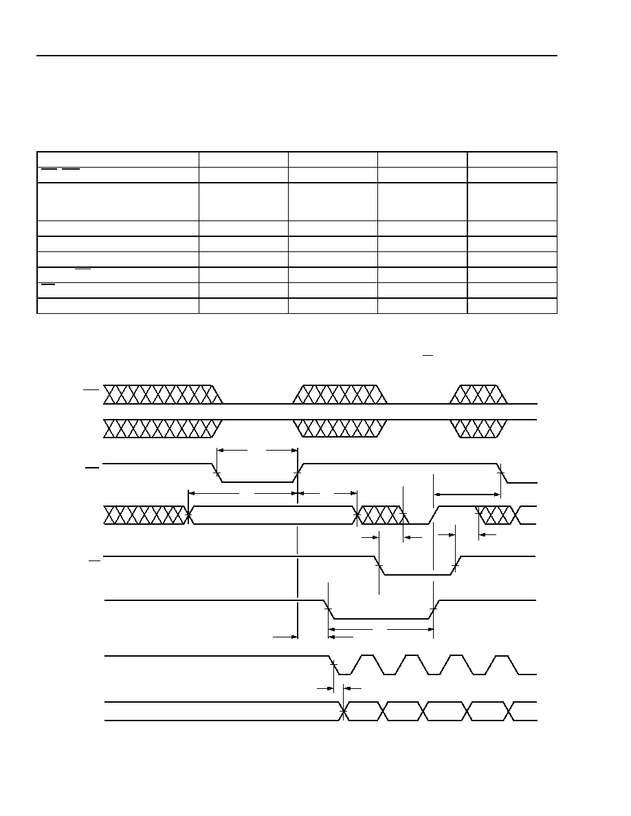
138
Lucent Technologies Inc.
Data Sheet
June 1999
ORCA Series 3C and 3T FPGAs
Timing Characteristics
(continued)
Table 63. Asynchronous Peripheral Configuration Mode Timing Characteristics
OR3Cxx Commercial: V
DD
= 5.0 V ± 5%, 0 ∞C
<
T
A
<
70 ∞C; Industrial: V
DD
= 5.0 V ± 10%, ≠40 ∞C
<
T
A
<
+85 ∞C.
OR3Txxx Commercial: V
DD
= 3.0 V to 3.6 V, 0 ∞C
<
T
A
<
70 ∞C; Industrial: V
DD
= 3.0 V to 3.6 V, ≠40 ∞C
<
T
A
<
+85
∞C.
* This parameter is valid whether the end of not RDY is determined from the RDY pin or from the D7 pin.
Notes:
Serial data is transmitted out on DOUT on the falling edge of CCLK after the byte is input on D[7:0].
D[6:0] timing is the same as the write data portion of the D7 waveform because D[6:0] are not enabled by
RD.
5-4533(F)
Figure 85. Asynchronous Peripheral Configuration Mode Timing Diagram
Parameter
Symbol
Min
Max
Unit
WR, CS0, and CS1 Pulse Width
T
WR
50.00
--
ns
D[7:0] Setup Time:
3Cxx
3Txxx
T
S
20.00
10.50
--
--
ns
ns
D[7:0] Hold Time
T
H
0.00
--
ns
RDY Delay
T
RDY
--
40.00
ns
RDY Low
T
B
1.00
8.00
CCLK Periods
Earliest WR After RDY Goes High*
T
WR2
0.00
--
ns
RD to D7 Enable/Disable
T
DEN
--
40.00
ns
CCLK to DOUT
T
D
--
5.00
ns
CS1
D7
CCLK
DOUT
CS0
RDY
D0
D1
D2
T
B
T
WR
T
S
T
H
T
RDY
WR
D7
T
D
PREVIOUS BYTE
T
WR2
WRITE DATA
D3
T
DEN
T
DEN
RD
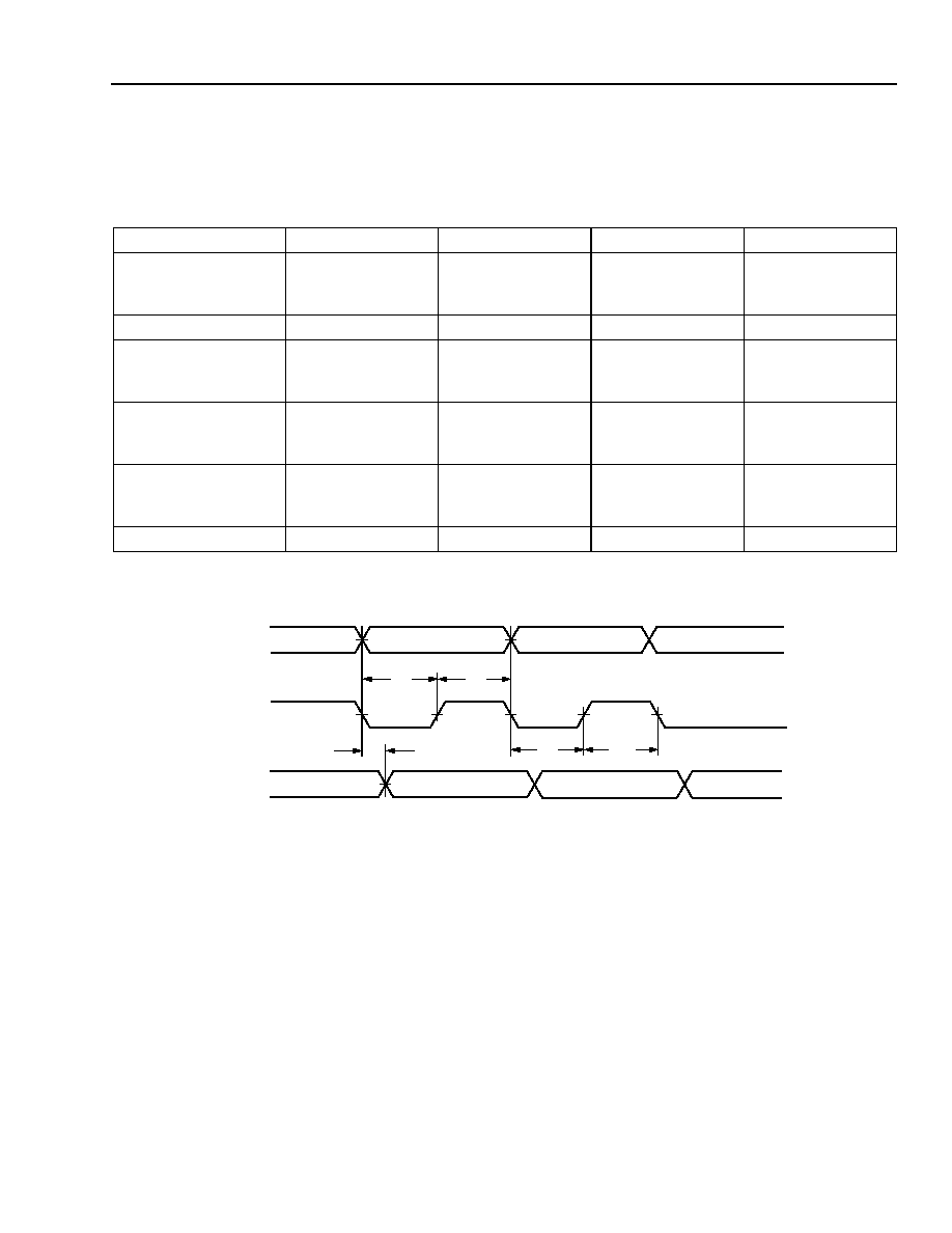
Lucent Technologies Inc.
139
Data Sheet
June 1999
ORCA Series 3C and 3T FPGAs
Timing Characteristics
(continued)
Table 64. Slave Serial Configuration Mode Timing Characteristics
OR3Cxx Commercial: V
DD
= 5.0 V ± 5%, 0 ∞C
<
T
A
<
70 ∞C; Industrial: V
DD
= 5.0 V ± 10%, ≠40 ∞C
<
T
A
<
+85 ∞C.
OR3Txxx Commercial: V
DD
= 3.0 V to 3.6 V, 0 ∞C
<
T
A
<
70 ∞C; Industrial: V
DD
= 3.0 V to 3.6 V, ≠40 ∞C
<
T
A
<
+85 ∞C.
Note: Serial configuration data is transmitted out on DOUT on the falling edge of CCLK after it is input on DIN.
5-4535(F).
Figure 86. Slave Serial Configuration Mode Timing Diagram
Parameter
Symbol
Min
Max
Unit
DIN Setup Time:
3Cxx
3Txxx
T
S
20.00
10.50
--
--
ns
ns
DIN Hold Time
T
H
0.00
--
ns
CCLK High Time:
3Cxx
3Txxx
T
CH
20.00
7.00
--
--
ns
ns
CCLK Low Time:
3Cxx
3Txxx
T
CL
20.00
7.00
--
--
ns
ns
CCLK Frequency:
3Cxx
3Txxx
F
C
--
--
25.00
66.00
MHz
MHz
CCLK to DOUT
T
D
--
20.00
ns
DIN
CCLK
DOUT
T
D
T
S
T
H
T
CL
T
CH
BIT N
BIT N
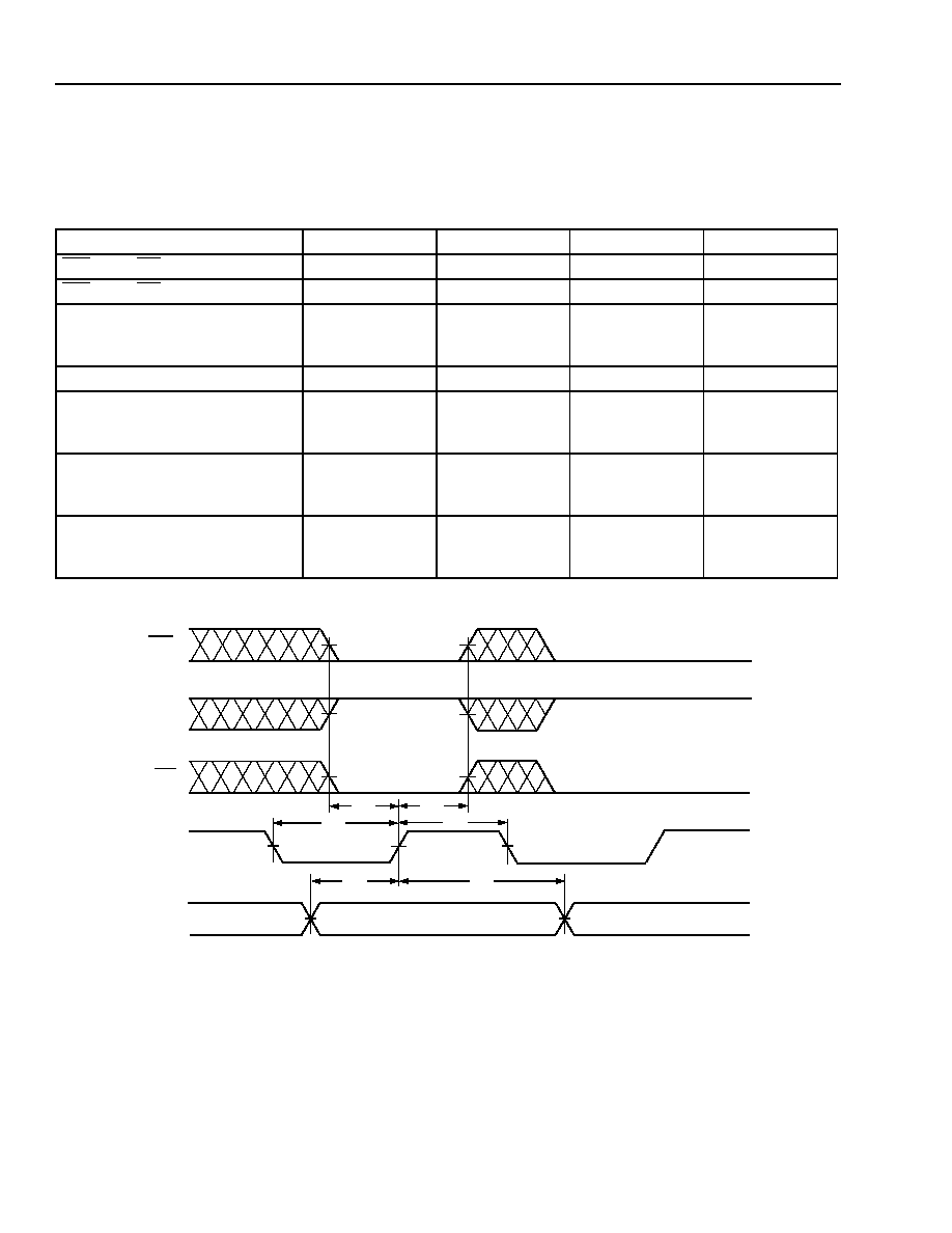
140
Lucent Technologies Inc.
Data Sheet
June 1999
ORCA Series 3C and 3T FPGAs
Timing Characteristics
(continued)
Table 65. Slave Parallel Configuration Mode Timing Characteristics
OR3Cxx Commercial: V
DD
= 5.0 V ± 5%, 0 ∞C
<
T
A
<
70 ∞C; Industrial: V
DD
= 5.0 V ± 10%, ≠40 ∞C
<
T
A
<
+85 ∞C.
OR3Txxx Commercial: V
DD
= 3.0 V to 3.6 V, 0 ∞C
<
T
A
<
70 ∞C; Industrial: V
DD
= 3.0 V to 3.6 V, ≠40 ∞C
<
T
A
<
+85
∞C.
Note: Daisy-chaining of FPGAs is not supported in this mode.
5-2848(F)
Figure 87. Slave Parallel Configuration Mode Timing Diagram
Parameter
Symbol
Min
Max
Unit
CS0
, CS1,
WR
Setup Time
T
S1
40.00
--
ns
CS0
, CS1,
WR
Hold Time
T
H1
20.00
--
ns
D[7:0] Setup Time:
3Cxx
3Txxx
T
S2
20.00
7.00
--
--
ns
ns
D[7:0] Hold Time
T
H2
0.00
--
ns
CCLK High Time:
3Cxx
3Txxx
T
CH
20.00
7.00
--
--
ns
ns
CCLK Low Time:
3Cxx
3Txxx
T
CL
20.00
7.00
--
--
ns
ns
CCLK Frequency:
3Cxx
3Txxx
F
C
--
--
25.00
66.00
MHz
MHz
T
S1
T
S2
T
H2
CS1
CCLK
D[7:0]
CS0
WR
T
CL
T
CH
T
H1

Lucent Technologies Inc.
141
Data Sheet
June 1999
ORCA Series 3C and 3T FPGAs
Timing Characteristics
(continued)
Microprocessor Interface (MPI) Configuration Timing Characteristics
For configuration timing using the MPI, consult Table 49. See Figures 67 through 74 for MPI timing diagrams.
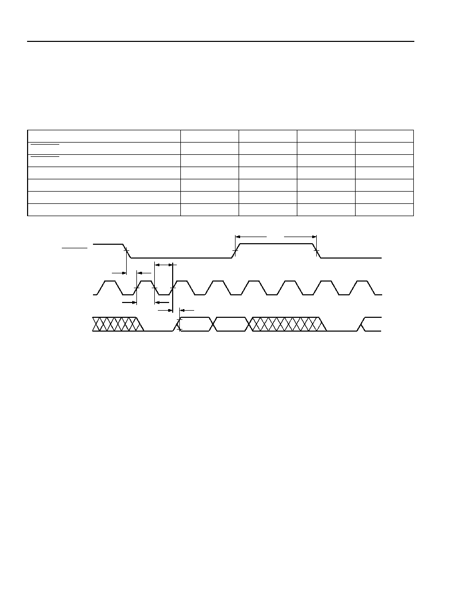
142
Lucent Technologies Inc.
Data Sheet
June 1999
ORCA Series 3C and 3T FPGAs
Timing Characteristics
(continued)
Readback Timing
Table 66. Readback Timing Characteristics
OR3Cxx Commercial: V
DD
= 5.0 V ± 5%, 0 ∞C
<
T
A
<
70 ∞C; Industrial: V
DD
= 5.0 V ± 10%, ≠40 ∞C
<
T
A
<
+85 ∞C.
OR3Txxx Commercial: V
DD
= 3.0 V to 3.6 V, 0 ∞C
<
T
A
<
70 ∞C; Industrial: V
DD
= 3.0 V to 3.6 V, ≠40 ∞C
<
T
A
<
+85
∞C.
5-4536(F)
Figure 88. Readback Timing Diagram
Parameter
Symbol
Min
Max
Unit
RD_CFG
to CCLK Setup Time
T
S
50.00
--
ns
RD_CFG
High Width to Abort Readback
T
RBA
2
--
CCLK cycles
CCLK Low Time
T
CL
40.00
--
ns
CCLK High Time
T
CH
40.00
--
ns
CCLK Frequency
F
C
--
12.50
MHz
CCLK to RD_DATA Delay
T
D
--
40.00
ns
T
D
T
CH
CCLK
RD_DATA
T
S
T
CL
RD_CFG
BIT 0
BIT 1
BIT 0
T
RBA
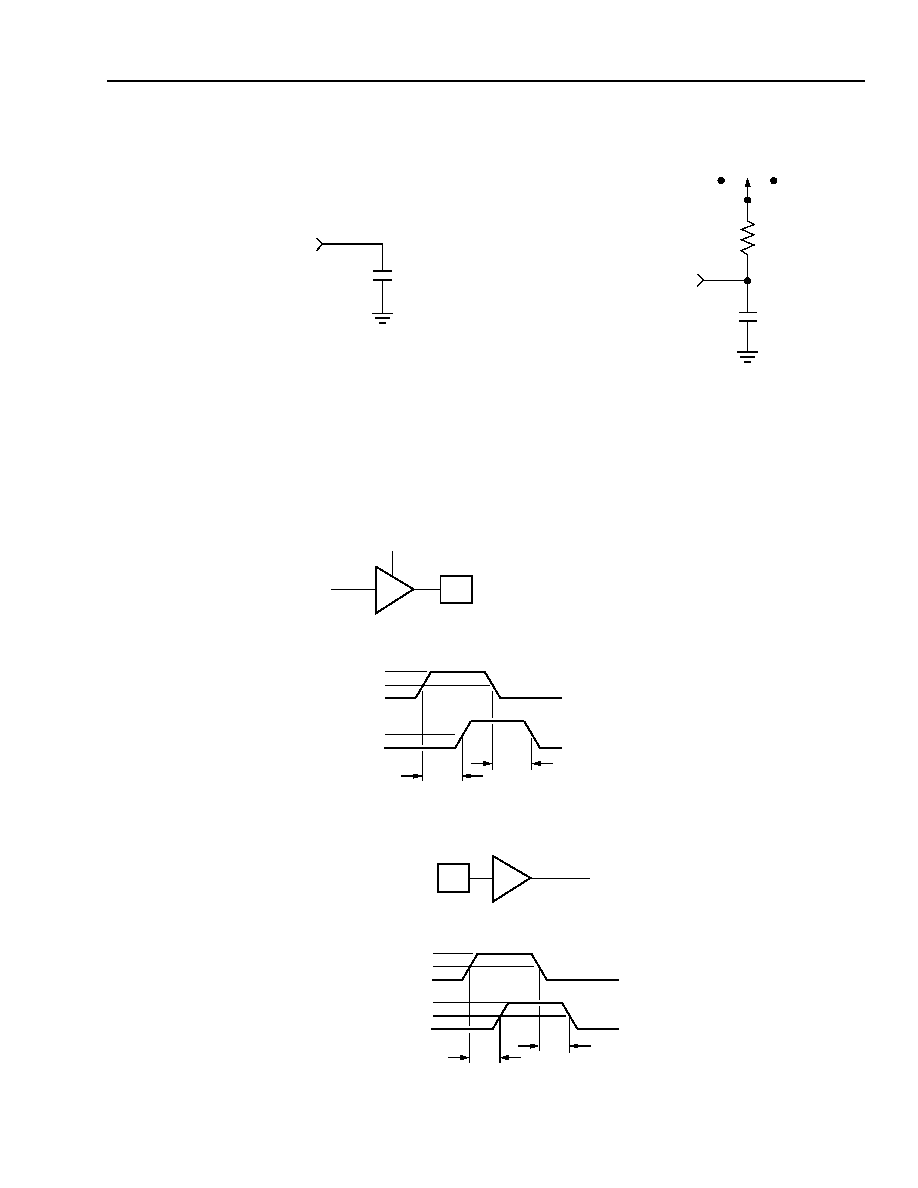
Lucent Technologies Inc.
143
Data Sheet
June 1999
ORCA Series 3C and 3T FPGAs
Input/Output Buffer Measurement Conditions
Note: Switch to V
DD
for
T
PLZ
/T
PZL
; switch to GND for T
PHZ
/T
PZH
.
5-3234(F)
Figure 89. ac Test Loads
5-3233.a(F)
Figure 90. Output Buffer Delays
5-3235(F)
Figure 91. Input Buffer Delays
50 pF
A. Load Used to Measure Propagation Delay
TO THE OUTPUT UNDER TEST
TO THE OUTPUT UNDER TEST
50 pF
V
CC
GND
1 k
B. Load Used to Measure Rising/Falling Edges
V
DD
T
PHH
V
DD
/2
V
SS
out[i]
PAD
OUT
1.5 V
0.0 V
T
PLL
PAD
out[i]
ac TEST LOADS (SHOWN ABOVE)
ts[i]
OUT
0.0 V
1.5 V
T
PHH
T
PLL
PAD
in[i]
IN
3.0 V
V
SS
V
DD
/2
V
DD
PAD IN
in[i]
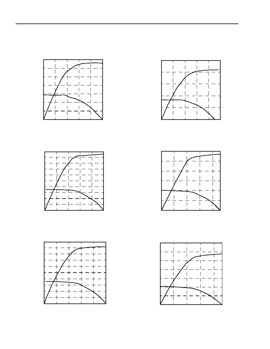
144
144
Lucent Technologies Inc.
Data Sheet
June 1999
ORCA Series 3C and 3T FPGAs
Output Buffer Characteristics
OR3Cxx
5-4634(F)
Figure 92. Sinklim (T
J
= 25 ∞C, V
DD
= 5.0 V)
5-4636(F)
Figure 93. Slewlim (T
J
= 25 ∞C, V
DD
= 5.0 V)
5-4638(F)
Figure 94. Fast (T
J
= 25 ∞C, V
DD
= 5.0 V)
5-4635(C)
Figure 95. Sinklim (T
J
= 125 ∞C, V
DD
= 4.5 V)
5-4637(F)
Figure 96. Slewlim (T
J
= 125 ∞C, V
DD
= 4.5 V)
5-4639(F)
Figure 97. Fast (T
J
= 125 ∞C, V
DD
= 4.5 V)
70
60
50
40
30
20
10
0
OUTPUT CURRENT
,
I
O
(mA)
0
1
2
3
4
5
OUTPUT VOLTAGE, V
O
(V)
I
OL
I
OH
250
225
150
100
50
0
O
UTP
UT CU
RR
ENT
,
I
O
(mA
)
0
1
2
3
4
OUTPUT VOLTAGE, V
O
(V)
I
OL
I
OH
5
200
175
125
75
25
250
225
150
100
50
0
OU
TPU
T
CU
RR
ENT
,
I
O
(mA
)
0
1
2
3
4
OUTPUT VOLTAGE, V
O
(V)
I
OL
I
OH
5
200
175
125
75
25
50
40
30
20
10
0
O
U
T
P
UT
CU
RR
EN
T
,
I
O
(
m
A)
0
1
2
3
4
OUTPUT VOLTAGE, V
O
(V)
I
OL
I
OH
5
150
125
100
75
50
0
OU
TPU
T
CU
RRE
NT
,
I
O
(mA
)
0
1
2
3
4
OUTPUT VOLTAGE, V
O
(V)
I
OL
I
OH
25
175
125
100
75
50
0
O
U
T
P
UT
CU
R
R
E
N
T
,
I
O
(mA
)
0
1
2
3
4
OUTPUT VOLTAGE, V
O
(V)
I
OL
I
OH
25
150
Lucent Technologies Inc.
145
Data Sheet
June 1999
ORCA Series 3C and 3T FPGAs
Output Buffer Characteristics
(continued)
OR3Txxx
5-6865(F)
Figure 98. Sinklim (T
J
= 25 ∞C, V
DD
= 3.3 V)
5-6967(F)
Figure 99. Slewlim (T
J
= 25 ∞C, V
DD
= 3.3 V)
5-6867(F)
Figure 100. Fast (T
J
= 25 ∞C, V
DD
= 3.3 V)
5-6866(F)
Figure 101. Sinklim (T
J
= 125 ∞C, V
DD
= 3.0 V)
5-6868(F)
Figure 102. Slewlim (T
J
= 125 ∞C, V
DD
= 3.0 V)
5-6868(F)
Figure 103. Fast (T
J
= 125 ∞C, V
DD
= 3.0 V)
0.0
0.5
1.0
1.5
2.0
2.5
3.0
3.5
0
20
40
60
110
OUTPUT VOLTAGE, V
O
(V)
I
OL
70
50
30
10
I
OH
OUT
P
UT
CU
RRENT
, I
O
(mA
)
80
90
100
0.0
0.5
1.0
1.5
2.0
2.5
3.0
0
40
80
OUTPUT VOLTAGE, V
O
(V)
I
OL
100
60
20
I
OH
OUT
P
UT
CURRE
NT
, I
O
(m
A
)
120
140
3.5
0.0
0.5
1.0
1.5
2.0
2.5
3.0
0
40
80
OUTPUT VOLTAGE, V
O
(V)
I
OL
100
60
20
I
OH
OUT
P
UT CU
RREN
T
,
I
O
(mA
)
120
140
3.5
0.0
0.5
1.0
1.5
2.0
2.5
3.0
0
20
40
60
OUTPUT VOLTAGE, V
O
(V)
I
OL
70
50
30
10
I
OH
OUT
P
U
T
CURR
ENT
,
I
O
(m
A
)
80
90
0.0
0.5
1.0
1.5
2.0
2.5
3.0
0
40
80
OUTPUT VOLTAGE, V
O
(V)
I
OL
100
60
20
I
OH
OUT
P
UT
CURRE
NT
, I
O
(m
A
)
120
0.0
0.5
1.0
1.5
2.0
2.5
3.0
0
40
80
OUTPUT VOLTAGE, V
O
(V)
I
OL
100
60
20
I
OH
O
U
T
P
U
T
CU
RR
E
N
T
,
I
O
(mA
)
120

146
146
Lucent Technologies Inc.
Data Sheet
June 1999
ORCA Series 3C and 3T FPGAs
Estimating Power Dissipation
OR3Cxx
The total operating power dissipated is estimated by
summing the standby (I
DDSB
), internal, and external
power dissipated. The internal and external power is
the power consumed in the PLCs and PICs, respec-
tively. In general, the standby power is small and may
be neglected. The total operating power is as follows:
P
T
=
P
PLC
+
P
PIC
The internal operating power is made up of two parts:
clock generation and PFU output power. The PFU out-
put power can be estimated based upon the number of
PFU outputs switching when driving an average fan-out
of two:
P
PFU
= 0.136 mW/MHz
For each PFU output that switches, 0.136 mW/MHz
needs to be multiplied times the frequency (in MHz)
that the output switches. Generally, this can be esti-
mated by using one-half the clock rate, multiplied by
some activity factor; for example, 20%.
The power dissipated by the clock generation circuitry
is based upon four parts: the fixed clock power, the
power/clock branch row or column, the clock power dis-
sipated in each PFU that uses this particular clock, and
the power from the subset of those PFUs that are con-
figured as synchronous memory. Therefore, the clock
power can be calculated for the four parts using the fol-
lowing equations:
OR3C55 Clock Power
P
= [0.183 mW/MHz
+ (0.235 mW/MHz/Branch) (# Branches)
+ (0.033 mW/MHz/PFU) (# PFUs)
+ (0.008 mW/MHz/PIO (# PIOs)]
For a quick estimate, the worst-case (typical circuit)
OR3C55 clock power
14.64 mW/MHz.
OR3C80 Clock Power
P
= [0.224 mW/MHz
+ (0.288 mW/MHz/Branch) (# Branches)
+ (0.033 mW/MHz/PFU) (# PFUs)
+ (0.008 mW/MHz/PIO (# PIOs)]
For a quick estimate, the worst-case (typical circuit)
OR3C80 clock power
21.06 mW/MHz.
The power dissipated in a PIC is the sum of the power
dissipated in the four PIOs in the PIC. This consists of
power dissipated by inputs and ac power dissipated by
outputs. The power dissipated in each PIO depends on
whether it is configured as an input, output, or input/
output. If a PIO is operating as an output, then there is
a power dissipation component for P
IN
, as well as
P
OUT
. This is because the output feeds back to the
input.
The power dissipated by a TTL input buffer is estimated
as:
P
TTL
= 2.2 mW + 0.17 mW/MHz
The power dissipated by an input buffer is estimated
as:
P
CMOS
= 0.17 mW/MHz
The ac power dissipation from an output or bidirec-
tional is estimated by the following:
P
OUT
= (C
L
+ 8.8 pF) x V
DD
2
x F Watts
where the unit for C
L
is farads, and the unit for F is Hz.
As an example of estimating power dissipation, sup-
pose that a fully utilized OR3C55 has an average of
six outputs for each of the 324 PFUs, that 10 clock
branches are used so that the clock is driven to the
entire PLC array, that 150 of the 324 PFUs have FFs
clocked at 40 MHz, and that the PFU outputs have an
average activity factor of 20%.
Twenty TTL-configured inputs, 20 CMOS-configured
inputs, 32 outputs driving 30 pF loads, and 16 bidirec-
tional I/Os driving 50 pF loads are also generated from
the 40 MHz clock with an average activity factor of
20%. All of the output PIOs are registered, and 30 of
the input PIOs are registered. The worst-case (V
DD
=
5.25 V) power dissipation is estimated as follows:
P
PFU
= 324 x 6 (0.136 mW/MHz x 20 MHz x 20%)
= 1057.54 mW
P
CLK
=
[0.183 mW/MHz + (0.235 mW/MHz ≠ Branch)
(10 Branches)
+ (0.033 mW/MHz ≠ PFU) (150 PFUs)
+ (0.008 mW/MHz/PIO (58 PIOs)]
= 317.88 mW
P
TTL
= 20 x [2.2 mW + (0.17 mW/MHz x 20 MHz x 20%)]
= 57.6 mW
P
CMOS
= 20 x [0.17 mW x 20 MHz x 20%]
= 13.6 mW
P
OUT
= 32 x [(30 pF + 8.8 pF) x (5.25)
2
x 20 MHz x 20%]
= 136.89 mW
P
BID
= 16 x [(50 pF + 8.8 pF) x (5.25)
2
x 20 MHz x 20%]
= 103.72 mW
Total
= 1.69 W

Lucent Technologies Inc.
147
Data Sheet
June 1999
ORCA Series 3C and 3T FPGAs
Estimating Power Dissipation
(continued)
OR3Txxx (Preliminary Information)
The total operating power dissipated is estimated by
summing the standby (I
DDSB
), internal, and external
power dissipated. The internal and external power is
the power consumed in the PLCs and PICs, respec-
tively. In general, the standby power is small and may
be neglected. The total operating power is as follows:
P
T
=
P
PLC
+
P
PIC
The internal operating power is made up of two parts:
clock generation and PFU output power. The PFU out-
put power can be estimated based upon the number of
PFU outputs switching when driving an average fan-out
of two:
P
PFU
= 0.068 mW/MHz
For each PFU output that switches, 0.068 mW/MHz
needs to be multiplied times the frequency (in MHz)
that the output switches. Generally, this can be esti-
mated by using one-half the clock rate, multiplied by
some activity factor; for example, 20%.
The power dissipated by the clock generation circuitry
is based upon four parts: the fixed clock power, the
power/clock branch row or column, the clock power dis-
sipated in each PFU that uses this particular clock, and
the power from the subset of those PFUs configured as
synchronous memory. Therefore, the clock power can
be calculated for the four parts using the following
equations.
OR3T20 Clock Power
P
= [0.38 mW/MHz
+ (0.045 mW/MHz/Branch) (# Branches)
+ (0.015 mW/MHz/PFU) (# PFUs)
+ (0.004 mW/MHz/PIO (# PIOs)]
For a quick estimate, the worst-case (typical circuit)
OR3T20 clock power
2.92 mW/MHz.
OR3T30 Clock Power
P
= [0.53 mW/MHz
+ (0.061 mW/MHz/Branch) (# Branches)
+ (0.015 mW/MHz/PFU) (# PFUs)
+ (0.004 mW/MHz/PIO (# PIOs)]
For a quick estimate, the worst-case (typical circuit)
OR3T30 clock power
3.98 mW/MHz.
OR3T55 Clock Power
P
= [0.88 mW/MHz
+ (0.102 mW/MHz/Branch) (# Branches)
+ (0.015 mW/MHz/PFU) (# PFUs)
+ (0.004 mW/MHz/PIO (# PIOs)]
For a quick estimate, the worst-case (typical circuit)
OR3T55 clock power
6.58 mW/MHz.
OR3T80 Clock Power
P
= [0.107 mW/MHz
+ (0.124 mW/MHz/Branch) (# Branches)
+ (0.015 mW/MHz/PFU) (# PFUs)
+ (0.004 mW/MHz/PIO (# PIOs)]
For a quick estimate, the worst-case (typical circuit)
OR3T80 clock power
9.47 mW/MHz.
OR3T125 Clock Power
P
= [0.167 mW/MHz
+ (0.193 mW/MHz/Branch) (# Branches)
+ (0.015 mW/MHz/PFU) (# PFUs)
+ (0.004 mW/MHz/PIO (# PIOs)]
For a quick estimate, the worst-case (typical circuit)
OR3T125 clock power
15.44 mW/MHz.
The power dissipated in a PIC is the sum of the power
dissipated in the four PIOs in the PIC. This consists of
power dissipated by inputs and ac power dissipated by
outputs. The power dissipated in each PIO depends on
whether it is configured as an input, output, or input/
output. If a PIO is operating as an output, then there is
a power dissipation component for P
IN
, as well as
P
OUT
. This is because the output feeds back to the
input.
The power dissipated by an input buffer (V
IH
= V
DD
≠
0.3 V or higher) is estimated as:
P
IN
= 0.09 mW/MHz
The ac power dissipation from an output or bidirec-
tional is estimated by the following:
P
OUT
= (C
L
+ 8.8 pF) x V
DD
2
x F Watts
where the unit for C
L
is farads, and the unit for F is Hz.

148
Lucent Technologies Inc.
Data Sheet
June 1999
ORCA Series 3C and 3T FPGAs
Estimating Power Dissipation
(continued)
As an example of estimating power dissipation, suppose that a fully utilized OR3T80 has an average of
six outputs for each of the 484 PFUs, that 12 clock branches are used so that the clock is driven to the entire PLC
array, that 250 of the 484 PFUs have FFs clocked at 40 MHz, and that the PFU outputs have an average activity
factor of 20%.
Eighty inputs, 40 of them used as 5 V tolerant inputs, 50 outputs driving 30 pF loads, and 30 bidirectional
I/Os driving 50 pF loads are also generated from the
40 MHz clock with an average activity factor of 20%. All of the output PIOs are registered, and 30 of the input PIOs
are registered.
The worst-case (V
DD
= 3.6 V) power dissipation is estimated as follows:
P
PFU
= 484 x 6 (0.068 mW/MHz x 20 MHz x 20%)
= 789.9 mW
P
CLK
=
[0.107 mW/MHz + (0.09 mW/MHz ≠ Branch)
(12 Branches)
+ (0.015 mW/MHz ≠ PFU) (250 PFUs)
+ (0.004 mW/MHz/PIO) (110 PIOs)]
= 230.43 mW
P
IN
= 80 x [0.09 mW/MHz x 20 MHz x 20%]
= 28.8 mW
P
OUT
= 50 x [(30 pF + 8.8 pF) x (3.6)
2
x 20 MHz x 20%]
= 100.57 mW
P
BID
= 30 x [(50 pF + 8.8 pF) x (3.6)
2
x 20 MHz x 20%]
= 91.45 mW
TOTAL
= 1.241 W
Lucent Technologies Inc.
149
Data Sheet
June 1999
ORCA Series 3C and 3T FPGAs
Pin Information
Pin Descriptions
This section describes the pins found on the Series 3 FPGAs. Any pin not described in this table is a user-program-
mable I/O. During configuration, the user-programmable I/Os are 3-stated with an internal pull-up resistor enabled.
If any pin is not used (or not bonded to a package pin), it is also 3-stated with an internal pull-up resistor enabled
after configuration.
Table 67. Pin Descriptions
Symbol
I/O
Description
Dedicated Pins
V
DD
--
Positive power supply.
GND
--
Ground supply.
V
DD
5
--
5 V tolerant select. V
DD
5 pin locations are shown for package compatibility with
OR2TxxA devices. Connections to 5 V power sources are not used for 5 V tolerant
I/Os in the OR3Txxx devices.
RESET
I
During configuration,
RESET
forces the restart of configuration and a pull-up is
enabled. After configuration,
RESET
can be used as a general FPGA input or as a
direct input, which causes all PLC latches/FFs to be asynchronously set/reset.
CCLK
I
In the master and asynchronous peripheral modes, CCLK is an output which
strobes configuration data in. In the slave or synchronous peripheral mode, CCLK
is input synchronous with the data on DIN or D[7:0]. In microprocessor mode, CCLK
is used internally and output for daisy-chain operation.
DONE
I
O
As an input, a low level on DONE delays FPGA start-up after configuration (see
Note).
As an active-high, open-drain output, a high level on this signal indicates that config-
uration is complete. DONE has an optional pull-up resistor.
PRGM
I
PRGM
is an active-low input that forces the restart of configuration and resets the
boundary-scan circuitry. This pin always has an active pull-up.
RD_CFG
I
This pin must be held high during device initialization until the
INIT
pin goes high.
This pin always has an active pull-up.
During configuration,
RD_CFG
is an active-low input that activates the TS_ALL func-
tion and 3-states all of the I/O.
After configuration,
RD_CFG
can be selected (via a bit stream option) to activate the
TS_ALL function as described above, or, if readback is enabled via a bit stream
option, a high-to-low transition on
RD_CFG
will initiate readback of the configuration
data, including PFU output states, starting with frame address 0.
RD_DATA/TDO
O
RD_DATA/TDO is a dual-function pin. If used for readback, RD_DATA provides con-
figuration data out. If used in boundary scan, TDO is test data out.
Special-Purpose Pins
M0, M1, M2
I
I/O
During powerup and initialization, M0--M2 are used to select the configuration
mode with their values latched on the rising edge of
INIT
; see Table 34 for the config-
uration modes. During configuration, a pull-up is enabled.
After configuration, these pins are user-programmable I/O (see Note).
Note: The FPGA States of Operation section contains more information on how to control these signals during start-up. The timing of DONE
release is controlled by one set of bit stream options, and the timing of the simultaneous release of all other configuration pins (and the
activation of all user I/Os) is controlled by a second set of options.

150
Lucent Technologies Inc.
Data Sheet
June 1999
ORCA Series 3C and 3T FPGAs
Pin Information
(continued)
Table 67. Pin Descriptions (continued)
Symbol
I/O
Description
Special-Purpose Pins (continued)
M3
I
I/O
During powerup and initialization, M3 is used to select the speed of the internal oscillator dur-
ing configuration with their values latched on the rising edge of
INIT
. When M3 is low, the
oscillator frequency is 10 MHz. When M3 is high, the oscillator is 1.25 MHz. During configura-
tion, a pull-up is enabled.
After configuration, this pin is a user-programmable I/O pin (see Note).
TDI, TCK,
TMS
I
I/O
If boundary scan is used, these pins are test data in, test clock, and test mode select inputs. If
boundary scan is not selected, all boundary-scan functions are inhibited once configuration is
complete. Even if boundary scan is not used, either TCK or TMS must be held at logic 1 dur-
ing configuration. Each pin has a pull-up enabled during configuration.
After configuration, these pins are user-programmable I/O (see Note).
RDY/RCLK/
MPI_ALE
O
O
I
I/O
During configuration in peripheral mode, RDY/RCLK indicates another byte can be written to
the FPGA. If a read operation is done when the device is selected, the same status is also
available on D7 in asynchronous peripheral mode.
During the master parallel configuration mode, RCLK is a read output signal to an external
memory. This output is not normally used.
In
i960
microprocessor mode, this pin acts as the address latch enable (ALE) input.
After configuration, if the MPI is not used, this pin is a user-programmable I/O pin (see Note).
HDC
O
I/O
High During Configuration is output high until configuration is complete. It is used as a control
output, indicating that configuration is not complete.
After configuration, this pin is a user-programmable I/O pin (see Note).
LDC
O
I/O
Low During Configuration
is output low until configuration is complete. It is used as a control out-
put, indicating that configuration is not complete.
After configuration, this pin is a user-programmable I/O pin (see Note).
INIT
I/O
I/O
INIT
is a bidirectional signal before and during configuration. During configuration, a pull-up is
enabled, but an external pull-up resistor is recommended. As an active-low open-drain out-
put,
INIT
is held low during power stabilization and internal clearing of memory. As an active-
low input,
INIT
holds the FPGA in the wait-state before the start of configuration.
After configuration, this pin is a user-programmable I/O pin (see Note).
Note: The FPGA States of Operation section contains more information on how to control these signals during start-up. The timing of DONE
release is controlled by one set of bit stream options, and the timing of the simultaneous release of all other configuration pins (and the
activation of all user I/Os) is controlled by a second set of options.
Lucent Technologies Inc.
151
Data Sheet
June 1999
ORCA Series 3C and 3T FPGAs
Special-Purpose Pins (continued)
CS0
, CS1
I
I/O
CS0
and CS1 are used in the asynchronous peripheral, slave parallel, and microprocessor
configuration modes. The FPGA is selected when
CS0
is low and CS1 is high. During config-
uration, a pull-up is enabled.
After configuration, these pins are user-programmable I/O pins (see Note).
RD
/
MPI_STRB
I
I
I/O
RD
is used in the asynchronous peripheral configuration mode. A low on
RD
changes D7 into
a status output. As a status indication, a high indicates ready, and a low indicates busy.
WR
and
RD
should not be used simultaneously. If they are, the write strobe overrides.
This pin is also used as the microprocessor interface (MPI) data transfer strobe. For
PowerPC
, it is the transfer start (TS). For
i960
, it is the address/data strobe (
ADS
).
After configuration, if the MPI is not used, this pin is a user-programmable I/O pin (see Note).
WR
I
I/O
WR
is used in the asynchronous peripheral configuration mode. When the FPGA is selected,
a low on the write strobe,
WR
, loads the data on D[7:0] inputs into an internal data buffer.
WR
and
RD
should not be used simultaneously. If they are, the write strobe overrides.
After configuration, this pin is a user-programmable I/O pin (see Note).
A[17:0]
O
I/O
During master parallel configuration mode, A[17:0] address the configuration EPROM. In
microprocessor interface (MPI) mode, many of the A[n] pins have alternate uses as described
below. See the Special Function Blocks section for more MPI information. During configura-
tion, if not in master parallel or an MPI configuration mode, these pins are 3-stated with a pull-
up enabled.
After configuration, the pins are user-programmable I/O pins (see Note).
Pin Information
(continued)
Table 67. Pin Descriptions (continued)
Symbol
I/O
Description
Note: The FPGA States of Operation section contains more information on how to control these signals during start-up. The timing of DONE
release is controlled by one set of bit stream options, and the timing of the simultaneous release of all other configuration pins (and the
activation of all user I/Os) is controlled by a second set of options.

152
Lucent Technologies Inc.
Data Sheet
June 1999
ORCA Series 3C and 3T FPGAs
Special-Purpose Pins (continued)
A11/
MPI_IRQ
O
I/O
MPI
active-low interrupt request output.
After configuration, if the MPI is not used, this pin is a user-programmable I/O pin (see Note).
A10/
MPI_BI
O
I/O
PowerPC
mode MPI burst inhibit output.
After configuration, if the MPI is not used, this pin is a user-programmable I/O pin (see Note).
A9/
MPI_ACK
O
I/O
In
PowerPC
mode MPI operation, this is the active-high transfer acknowledge (
TA
) output. For
i960
MPI operation, it is the active-low ready/record (
RDYRCV
) output.
After configuration, if the MPI is not used, this pin is a user-programmable I/O pin (see Note).
A8/MPI_RW
I
I/O
In
PowerPC
mode MPI operation, this is the active-low write/active-high read control signals.
For
i960
operation, it is the active-high write/active-low read control signal.
After configuration, if the MPI is not used, this pin is a user-programmable I/O pin (see Note).
A7/MPI_CLK
I
I/O
This is the clock used for the synchronous MPI interface. For
PowerPC
, it is the CLKOUT
signal. For
i960
, it is the system clock that is chosen for the
i960
external bus interface.
After configuration, if the MPI is not used, this pin is a user-programmable I/O pin (see Note).
A[4:0]
I
I/O
For
PowerPC
operation, these are the
PowerPC
address inputs. The address bit mapping (in
PowerPC
/FPGA notation) is A[31]/A[0], A[30]/A[1], A[29]/A[2], A[28]/A[3], A[27]/A[4]. Note
that A[27]/A[4] is the MSB of the address. The A[4:2] inputs are not used in
i960
MPI
mode.
After configuration, if the MPI is not used, this pin is a user-programmable I/O pin (see Note).
A[1:0]/
MPI_BE[1:0]
I
I/O
For
i960
operation,
MPI_BE[1:0]
provide the
i960
byte enable signals,
BE[1:0]
, that are used as
address bits A[1:0] in
i960
byte-wide operation.
After configuration, if the MPI is not used, this pin is a user-programmable I/O pin (see Note).
D[7:0]
I
I/O
During master parallel, peripheral, and slave parallel configuration modes, D[7:0] receive
configuration data, and each pin has a pull-up enabled. During serial configuration modes, D0
is the DIN input. D[7:0] are also the data pins for
PowerPC
microprocessor mode and the
address/data pins for
i960
microprocessor mode.
After configuration, the pins are user-programmable I/O pins (see Note).
DIN
I
I/O
During slave serial or master serial configuration modes, DIN accepts serial configuration
data synchronous with CCLK. During parallel configuration modes, DIN is the D0 input. Dur-
ing configuration, a pull-up is enabled.
After configuration, this pin is a user-programmable I/O pin (see Note).
DOUT
O
I/O
During configuration, DOUT is the serial data output that can drive the DIN of daisy-chained
slave LCA devices. Data out on DOUT changes on the falling edge of CCLK.
After configuration, DOUT is a user-programmable I/O pin (see Note).
Pin Information
(continued)
Table 67. Pin Descriptions (continued)
Symbol
I/O
Description
Note: The FPGA States of Operation section contains more information on how to control these signals during start-up. The timing of DONE
release is controlled by one set of bit stream options, and the timing of the simultaneous release of all other configuration pins (and the
activation of all user I/Os) is controlled by a second set of options.

Lucent Technologies Inc.
153
Data Sheet
June 1999
ORCA Series 3C and 3T FPGAs
Pin Information
(continued)
Package Compatibility
Table 68 provides the number of user I/Os available for the
ORCA
Series 3 FPGAs for each available package.
Each package has six dedicated configuration pins.
Tables 70--75 provide the package pin and pin function for the
ORCA
Series 3 FPGAs and packages. The bond
pad name is identified in the PIC nomenclature used in the
ORCA
Foundry design editor.
When the number of FPGA bond pads exceeds the number of package pins, bond pads are unused. When the
number of package pins exceeds the number of bond pads, package pins are left unconnected (no connects).
When a package pin is to be left as a no connect for a specific die, it is indicated as a note in the device pad column
for the FPGA. The tables provide no information on unused pads.
Table 68.
ORCA
I/Os Summary
*User I/O count includes four ExpressCLK inputs.
Device
208-Pin
SQFP/SQPF2
240-Pin
SQFP/SQFP2
256-Pin
PBGA
352-Pin
PBGA
432-Pin
EBGA
600-Pin
EBGA
OR3T20
User I/Os*
171
192
192
192
--
--
V
DD
/V
SS
31
40
26
48
--
--
Configuration
6
6
6
6
--
--
Unused
0
2
32
106
--
--
OR3T30
User I/Os*
171
192
221
224
--
--
V
DD
/V
SS
31
40
26
48
--
--
Configuration
6
6
6
6
--
--
Unused
0
2
3
74
--
--
OR3C/T55
User I/Os*
171
192
223
288
--
--
V
DD
/V
SS
31
42
26
48
--
--
Configuration
6
6
6
6
--
--
Unused
0
0
1
10
--
--
OR3C/T80
User I/Os*
171
192
--
298
342
--
V
DD
/V
SS
31
42
--
48
84
--
Configuration
6
6
--
6
6
--
Unused
0
0
--
0
0
--
OR3T125
User I/Os*
171
192
--
298
342
448
V
DD
/V
SS
31
42
--
48
84
140
Configuration
6
6
--
6
6
6
Unused
0
0
--
0
0
6

154
Lucent Technologies Inc.
Data Sheet
June 1999
ORCA Series 3C and 3T FPGAs
Pin Information
(continued)
Compatibility with OR2C/TxxA Series
The pinouts shown for the OR3Cxx and OR3Txxx devices are consistent with the OR2C/TxxA Series for all devices
offered in the same packages. This includes the following pins: V
DD
, V
SS
, V
DD
5 (OR2TxxA Series only), and all
configuration pins.
The following restrictions apply:
1. There are two configuration modes supported in the OR2C/TxxA Series that are not supported in Series 3: mas-
ter parallel down and synchronous peripheral modes. The Series 3 FPGAs have two new microprocessor inter-
face (MPI) configuration modes that are unavailable in the OR2C/TxxA Series.
2. There are four pins--one per each device side--that are user I/O in the OR2C/TxxA Series which can only be
used as fast dedicated clocks or global inputs in Series 3. These pins are also used to drive the ExpressCLK to
the I/O FFs on their given side of the device. These four middle ExpressCLK pins should not be used to connect
to a programmable clock manager (PCM). A corner ExpressCLK input should be used instead (see item 3
below). See Table 69 for a list of these pins in each package.
3. There are two other pins that are user I/O in both the OR2C/TxxA and Series 3 but also have optional added
functionality. Each of these pins drives the ExpressCLKs on two sides of the device. They also have fast connec-
tivity to the programmable clock manager (PCM). See Table 69 for a list of these pins in each package.
Table 69. Series 3 ExpressCLK Pins
Pin Name/
Package
208-Pin
SQFP/SQFP2
240-Pin
SQFP/SQFP2
256-Pin
PBGA
352-Pin
PBGA
432-Pin
EBGA
600-Pin
EBGA
I-ECKL
22
26
K3
N2
R29
U33
I-ECKB
80
91
W11
AE14
AH16
AM18
I-ECKR
131
152
K18
N23
T2
V2
I-ECKT
178
207
B11
B14
C15
C17
I/O-SECKLL
49
56
W1
AB4
AG29
AK34
I/O-SECKUR
159
184
A19
A25
D5
D5

Lucent Technologies Inc.
155
Data Sheet
June 1999
ORCA Series 3C and 3T FPGAs
Pin Information
(continued)
Table 70. OR3T20, OR3T30, OR3C/T55, OR3C/T80, and OR3T125 208-Pin SQFP/SQFP2 Pinout
Pin
OR3T20
Pad
OR3T30
Pad
OR3C/T55
Pad
OR3C/T80
Pad
OR3T125
Pad
Function
1
V
SS
V
SS
V
SS
V
SS
V
SS
V
SS
2
V
SS
V
SS
V
SS
V
SS
V
SS
V
SS
3
PL1D
PL1D
PL1D
PL1D
PL1D
I/O
4
PL1A
PL2D
PL2D
PL2D
PL2D
I/O-A0/
MPI_BE0
5
PL2D
PL4D
PL3D
PL4D
PL4D
I/O
6
PL2C
PL5D
PL3A
PL4A
PL5D
I/O
7
PL2A
PL7D
PL4A
PL5A
PL7D
I/O-A1/
MPI_BE1
8
PL3D
PL8A
PL5A
PL6A
PL8A
I/O-A2
9
PL3C
PL9D
PL6D
PL7D
PL9D
I/O
10
PL3B
PL9B
PL6B
PL7B
PL9B
I/O
11
PL3A
PL9A
PL6A
PL7A
PL9A
I/O-A3
12
V
DD
V
DD
V
DD
V
DD
V
DD
V
DD
13
PL4D
PL10D
PL7D
PL8D
PL10D
I/O
14
PL4C
PL10A
PL7C
PL8A
PL10A
I/O
15
PL4B
PL11D
PL7B
PL9D
PL11D
I/O
16
PL4A
PL11A
PL7A
PL9B
PL11A
I/O-A4
17
PL5D
PL12D
PL8D
PL9A
PL12D
I/O-A5
18
PL5C
PL12A
PL8C
PL10C
PL12A
I/O
19
PL5B
PL13D
PL8B
PL10B
PL13D
I/O
20
PL5A
PL13A
PL8A
PL10A
PL13A
I/O-A6
21
V
SS
V
SS
V
SS
V
SS
V
SS
V
SS
22
PECKL
PECKL
PECKL
PECKL
PECKL
I-ECKL
23
PL6C
PL14C
PL9C
PL11C
PL14C
I/O
24
PL6B
PL14B
PL9B
PL11B
PL14B
I/O
25
PL6A
PL14A
PL9A
PL11A
PL14A
I/O-A7/MPI_CLK
26
V
DD
V
DD
V
DD
V
DD
V
DD
V
DD
27
PL7D
PL15D
PL10D
PL12D
PL15D
I/O
28
PL7C
PL15C
PL10C
PL12C
PL15C
I/O
29
PL7B
PL15B
PL10B
PL12B
PL15B
I/O
30
PL7A
PL15A
PL10A
PL12A
PL15A
I/O-A8/MPI_RW
31
V
SS
V
SS
V
SS
V
SS
V
SS
V
SS
32
PL8D
PL16D
PL11D
PL13D
PL16D
I/O-A9/
MPI_ACK
33
PL8C
PL16A
PL11C
PL13B
PL16A
I/O
34
PL8B
PL17D
PL11B
PL13A
PL17D
I/O
35
PL8A
PL17A
PL11A
PL14C
PL17A
I/O-A10/
MPI_BI
36
PL9D
PL18D
PL12D
PL14B
PL18D
I/O
37
PL9C
PL18A
PL12C
PL15C
PL18A
I/O
38
PL9B
PL19D
PL12B
PL15B
PL19D
I/O
39
PL9A
PL19A
PL12A
PL15A
PL19A
I/O-A11/
MPI_IRQ

156
Lucent Technologies Inc.
Data Sheet
June 1999
ORCA Series 3C and 3T FPGAs
40
V
DD
V
DD
V
DD
V
DD
V
DD
V
DD
41
PL10D
PL20D
PL13D
PL16D
PL20D
I/O-A12
42
PL10C
PL20B
PL13B
PL16B
PL20B
I/O
43
PL10B
PL21D
PL14D
PL17D
PL21D
I/O
44
PL10A
PL21B
PL14B
PL17B
PL21B
I/O-A13
45
PL11D
PL22D
PL15D
PL18D
PL22D
I/O
46
PL11A
PL24A
PL16D
PL19D
PL24A
I/O-A14
47
PL12D
PL26D
PL17D
PL20D
PL26D
I/O
48
PL12C
PL27D
PL17A
PL21D
PL27D
I/O
49
PL12B
PL27A
PL18C
PL21A
PL27A
I/O-SECKLL
50
PL12A
PL28A
PL18A
PL22A
PL28A
I/O-A15
51
V
SS
V
SS
V
SS
V
SS
V
SS
V
SS
52
PCCLK
PCCLK
PCCLK
PCCLK
PCCLK
CCLK
53
V
SS
V
SS
V
SS
V
SS
V
SS
V
SS
54
V
SS
V
SS
V
SS
V
SS
V
SS
V
SS
55
PB1A
PB1A
PB1A
PB1A
PB1A
I/O-A16
56
PB1B
PB2A
PB1D
PB2A
PB2A
I/O
57
PB1C
PB2D
PB2A
PB2D
PB2D
I/O
58
PB1D
PB3D
PB2D
PB3D
PB3D
I/O
59
PB2A
PB4D
PB3D
PB4D
PB4D
I/O-A17
60
PB2D
PB5D
PB4D
PB5D
PB5D
I/O
61
PB3A
PB6D
PB5B
PB6B
PB6D
I/O
62
PB3B
PB7D
PB5D
PB6D
PB7D
I/O
63
PB3C
PB8D
PB6B
PB7B
PB8D
I/O
64
PB3D
PB9D
PB6D
PB7D
PB9D
I/O
65
V
DD
V
DD
V
DD
V
DD
V
DD
V
DD
66
PB4A
PB10A
PB7A
PB8A
PB10A
I/O
67
PB4B
PB10D
PB7B
PB8D
PB10D
I/O
68
PB4C
PB11A
PB7C
PB9A
PB11A
I/O
69
PB4D
PB11D
PB7D
PB9C
PB11D
I/O
70
PB5A
PB12A
PB8A
PB9D
PB12A
I/O
71
PB5B
PB12D
PB8B
PB10A
PB12D
I/O
72
PB5C
PB13A
PB8C
PB10B
PB13A
I/O
73
PB5D
PB13D
PB8D
PB10D
PB13D
I/O
74
V
SS
V
SS
V
SS
V
SS
V
SS
V
SS
75
PB6A
PB14A
PB9A
PB11A
PB14A
I/O
76
PB6B
PB14B
PB9B
PB11B
PB14B
I/O
77
PB6C
PB14C
PB9C
PB11C
PB14C
I/O
78
PB6D
PB14D
PB9D
PB11D
PB14D
I/O
Pin
OR3T20
Pad
OR3T30
Pad
OR3C/T55
Pad
OR3C/T80
Pad
OR3T125
Pad
Function
Pin Information
(continued)
Table 70. OR3T20, OR3T30, OR3C/T55, OR3C/T80, and OR3T125, 208-Pin SQFP/SQFP2 Pinout (continued)

Lucent Technologies Inc.
157
Data Sheet
June 1999
ORCA Series 3C and 3T FPGAs
79
V
SS
V
SS
V
SS
V
SS
V
SS
V
SS
80
PECKB
PECKB
PECKB
PECKB
PECKB
I-ECKB
81
PB7B
PB15B
PB10B
PB12B
PB15B
I/O
82
PB7C
PB15C
PB10C
PB12C
PB15C
I/O
83
PB7D
PB15D
PB10D
PB12D
PB15D
I/O
84
V
SS
V
SS
V
SS
V
SS
V
SS
V
SS
85
PB8A
PB16A
PB11A
PB13A
PB16A
I/O
86
PB8B
PB16D
PB11B
PB13B
PB16D
I/O
87
PB8C
PB17A
PB11C
PB13C
PB17A
I/O
88
PB8D
PB17D
PB11D
PB14A
PB17D
I/O
89
PB9A
PB18A
PB12A
PB14B
PB18A
I/O-HDC
90
PB9B
PB18D
PB12B
PB14D
PB18D
I/O
91
PB9C
PB19A
PB12C
PB15A
PB19A
I/O
92
PB9D
PB19D
PB12D
PB15D
PB19D
I/O
93
V
DD
V
DD
V
DD
V
DD
V
DD
V
DD
94
PB10A
PB20A
PB13A
PB16A
PB20A
I/O-
LDC
95
PB10B
PB21D
PB13D
PB16D
PB21D
I/O
96
PB10C
PB22A
PB14A
PB17A
PB22A
I/O
97
PB10D
PB23D
PB14D
PB17D
PB23D
I/O
98
PB11A
PB24A
PB15A
PB18A
PB24A
I/O-
INIT
99
PB11C
PB25A
PB16A
PB19A
PB25A
I/O
100
PB11D
PB26A
PB17A
PB20A
PB26A
I/O
101
PB12A
PB27D
PB18A
PB21D
PB27D
I/O
102
PB12D
PB28D
PB18D
PB22D
PB28D
I/O
103
V
SS
V
SS
V
SS
V
SS
V
SS
V
SS
104
PDONE
PDONE
PDONE
PDONE
PDONE
DONE
105
V
SS
V
SS
V
SS
V
SS
V
SS
V
SS
106
PRESETN
PRESETN
PRESETN
PRESETN
PRESETN
RESET
107
PPRGMN
PPRGMN
PPRGMN
PPRGMN
PPRGMN
PRGM
108
PR12A
PR28A
PR18A
PR22A
PR28A
I/O-M0
109
PR12D
PR27A
PR18D
PR21A
PR27A
I/O
110
PR11A
PR26A
PR17B
PR20A
PR26A
I/O
111
PR11B
PR25A
PR16A
PR19A
PR25A
I/O
112
PR10A
PR22D
PR15D
PR18D
PR22D
I/O-M1
113
PR10B
PR21A
PR14A
PR17A
PR21A
I/O
114
PR10C
PR21D
PR14D
PR17D
PR21D
I/O
115
PR10D
PR20A
PR13A
PR16A
PR20A
I/O
116
V
DD
V
DD
V
DD
V
DD
V
DD
V
DD
117
PR9A
PR19A
PR12A
PR15A
PR19A
I/O-M2
Pin
OR3T20
Pad
OR3T30
Pad
OR3C/T55
Pad
OR3C/T80
Pad
OR3T125
Pad
Function
Pin Information
(continued)
Table 70. OR3T20, OR3T30, OR3C/T55, OR3C/T80, and OR3T125 208-Pin SQFP/SQFP2 Pinout (continued)

158
Lucent Technologies Inc.
Data Sheet
June 1999
ORCA Series 3C and 3T FPGAs
118
PR9B
PR19D
PR12B
PR15D
PR19D
I/O
119
PR9C
PR18A
PR12C
PR14A
PR18A
I/O
120
PR9D
PR18D
PR12D
PR14C
PR18D
I/O
121
PR8A
PR17A
PR11A
PR14D
PR17A
I/O-M3
122
PR8B
PR17D
PR11B
PR13A
PR17D
I/O
123
PR8C
PR16A
PR11C
PR13B
PR16A
I/O
124
PR8D
PR16D
PR11D
PR13D
PR16D
I/O
125
V
SS
V
SS
V
SS
V
SS
V
SS
V
SS
126
PR7A
PR15A
PR10A
PR12A
PR15A
I/O
127
PR7B
PR15B
PR10B
PR12B
PR15B
I/O
128
PR7C
PR15C
PR10C
PR12C
PR15C
I/O
129
PR7D
PR15D
PR10D
PR12D
PR15D
I/O
130
V
DD
V
DD
V
DD
V
DD
V
DD
V
DD
131
PECKR
PECKR
PECKR
PECKR
PECKR
I-ECKR
132
PR6B
PR14B
PR9B
PR11B
PR14B
I/O
133
PR6C
PR14C
PR9C
PR11C
PR14C
I/O
134
PR6D
PR14D
PR9D
PR11D
PR14D
I/O
135
V
SS
V
SS
V
SS
V
SS
V
SS
V
SS
136
PR5A
PR13A
PR8A
PR10A
PR13A
I/O
137
PR5B
PR13D
PR8B
PR10C
PR13D
I/O
138
PR5C
PR12A
PR8C
PR10D
PR12A
I/O
139
PR5D
PR12D
PR8D
PR9B
PR12D
I/O
140
PR4A
PR11A
PR7A
PR9C
PR11A
I/O-CS1
141
PR4B
PR11D
PR7B
PR9D
PR11D
I/O
142
PR4C
PR10A
PR7C
PR8A
PR10A
I/O
143
PR4D
PR10D
PR7D
PR8D
PR10D
I/O
144
V
DD
V
DD
V
DD
V
DD
V
DD
V
DD
145
PR3A
PR9A
PR6A
PR7A
PR9A
I/O-
CS0
146
PR3B
PR9B
PR6B
PR7B
PR9B
I/O
147
PR3C
PR8B
PR5B
PR6B
PR8B
I/O
148
PR3D
PR8D
PR5D
PR6D
PR8D
I/O
149
PR2A
PR7A
PR4A
PR5A
PR7A
I/O-
RD
/
MPI_STRB
150
PR2C
PR5A
PR4D
PR5D
PR5A
I/O
151
PR2D
PR4A
PR3A
PR4A
PR4A
I/O
152
PR1A
PR3A
PR2A
PR3A
PR3A
I/O-WR
153
PR1C
PR2A
PR2C
PR2A
PR2A
I/O
154
PR1D
PR1A
PR1A
PR1A
PR1A
I/O
155
V
SS
V
SS
V
SS
V
SS
V
SS
V
SS
156
PRD_CFGN
PRD_CFGN
PRD_CFGN
PRD_CFGN
PRD_CFGN
RD_CFG
Pin
OR3T20
Pad
OR3T30
Pad
OR3C/T55
Pad
OR3C/T80
Pad
OR3T125
Pad
Function
Pin Information
(continued)
Table 70. OR3T20, OR3T30, OR3C/T55, OR3C/T80, and OR3T125 208-Pin SQFP/SQFP2 Pinout (continued)

Lucent Technologies Inc.
159
Data Sheet
June 1999
ORCA Series 3C and 3T FPGAs
157
V
SS
V
SS
V
SS
V
SS
V
SS
V
SS
158
V
SS
V
SS
V
SS
V
SS
V
SS
V
SS
159
PT12D
PT28D
PT18D
PT22D
PT28D
I/O-SECKUR
160
PT12A
PT27A
PT17D
PT21A
PT27A
I/O-RDY/RCLK/MPI_ALE
161
PT11D
PT25D
PT16D
PT19D
PT25D
I/O
162
PT11C
PT25A
PT16A
PT19A
PT25A
I/O
163
PT11A
PT24D
PT15D
PT18D
PT24D
I/O-D7
164
PT10D
PT23D
PT14D
PT17D
PT23D
I/O
165
PT10C
PT22D
PT14A
PT17A
PT22D
I/O
166
PT10B
PT21D
PT13D
PT16D
PT21D
I/O
167
PT10A
PT20D
PT13B
PT16B
PT20D
I/O-D6
168
V
DD
V
DD
V
DD
V
DD
V
DD
V
DD
169
PT9D
PT19D
PT12D
PT15D
PT19D
I/O
170
PT9C
PT19A
PT12C
PT15B
PT19A
I/O
171
PT9B
PT18D
PT12B
PT15A
PT18D
I/O
172
PT9A
PT18A
PT12A
PT14C
PT18A
I/O-D5
173
PT8D
PT17D
PT11D
PT14B
PT17D
I/O
174
PT8C
PT17A
PT11C
PT13D
PT17A
I/O
175
PT8B
PT16D
PT11B
PT13C
PT16D
I/O
176
PT8A
PT16A
PT11A
PT13A
PT16A
I/O-D4
177
V
SS
V
SS
V
SS
V
SS
V
SS
V
SS
178
PECKT
PECKT
PECKT
PECKT
PECKT
I-ECKT
179
PT7C
PT15C
PT10C
PT12C
PT15C
I/O
180
PT7B
PT15B
PT10B
PT12B
PT15B
I/O
181
PT7A
PT15A
PT10A
PT12A
PT15A
I/O-D3
182
V
SS
V
SS
V
SS
V
SS
V
SS
V
SS
183
PT6D
PT14D
PT9D
PT11D
PT14D
I/O
184
PT6C
PT14C
PT9C
PT11C
PT14C
I/O
185
PT6B
PT14B
PT9B
PT11B
PT14B
I/O
186
PT6A
PT14A
PT9A
PT11A
PT14A
I/O-D2
187
V
SS
V
SS
V
SS
V
SS
V
SS
V
SS
188
PT5D
PT13D
PT8D
PT10D
PT13D
I/O-D1
189
PT5C
PT13A
PT8C
PT10B
PT13A
I/O
190
PT5B
PT12D
PT8B
PT10A
PT12D
I/O
191
PT5A
PT12A
PT8A
PT9C
PT12A
I/O-D0/DIN
192
PT4D
PT11D
PT7D
PT9B
PT11D
I/O
193
PT4C
PT11A
PT7C
PT8D
PT11A
I/O
194
PT4B
PT10D
PT7B
PT8C
PT10D
I/O
195
PT4A
PT10A
PT7A
PT8A
PT10A
I/O-DOUT
196
V
DD
V
DD
V
DD
V
DD
V
DD
V
DD
Pin
OR3T20
Pad
OR3T30
Pad
OR3C/T55
Pad
OR3C/T80
Pad
OR3T125
Pad
Function
Pin Information
(continued)
Table 70. OR3T20, OR3T30, OR3C/T55, OR3C/T80, and OR3T125 208-Pin SQFP/SQFP2 Pinout (continued)

160
Lucent Technologies Inc.
Data Sheet
June 1999
ORCA Series 3C and 3T FPGAs
197
PT3D
PT9D
PT6D
PT7D
PT9D
I/O
198
PT3C
PT8A
PT6A
PT7A
PT8A
I/O
199
PT3B
PT7A
PT5C
PT6C
PT7A
I/O
200
PT3A
PT6A
PT5A
PT6A
PT6A
I/O-TDI
201
PT2D
PT5A
PT4A
PT5A
PT5A
I/O
202
PT2A
PT4A
PT3A
PT4A
PT4A
I/O-TMS
203
PT1D
PT3A
PT2C
PT3A
PT3A
I/O
204
PT1C
PT2A
PT2A
PT2A
PT2A
I/O
205
PT1B
PT1D
PT1D
PT1D
PT1D
I/O
206
PT1A
PT1A
PT1A
PT1A
PT1A
I/O-TCK
207
V
SS
V
SS
V
SS
V
SS
V
SS
V
SS
208
PRD_DATA
PRD_DATA
PRD_DATA
PRD_DATA
PRD_DATA
RD_DATA/TDO
Pin
OR3T20
Pad
OR3T30
Pad
OR3C/T55
Pad
OR3C/T80
Pad
OR3T125
Pad
Function
Pin Information
(continued)
Table 70. OR3T20, OR3T30, OR3C/T55, OR3C/T80, and OR3T125 208-Pin SQFP/SQFP2 Pinout (continued)

Lucent Technologies Inc.
161
Data Sheet
June 1999
ORCA Series 3C and 3T FPGAs
Pin Information
(continued)
Table 71. OR3T20, OR3T30, OR3C/T55, OR3C/T80, and OR3T125 240-Pin SQFP/SQFP2 Pinout
Pin
OR3T20
Pad
OR3T30
Pad
OR3C/T55
Pad
OR3C/T80
Pad
OR3T125
Pad
Function
1
V
SS
V
SS
V
SS
V
SS
V
SS
V
SS
2
V
DD
V
DD
V
DD
V
DD
V
DD
V
DD
3
PL1D
PL1D
PL1D
PL1D
PL1D
I/O
4
PL1C
PL1B
PL1C
PL1C
PL1C
I/O
5
PL1B
PL1A
PL1B
PL1B
PL1B
I/O
6
PL1A
PL2D
PL2D
PL2D
PL2D
I/O-A0/
MPI_BE0
7
V
SS
V
SS
V
SS
V
SS
V
SS
V
SS
8
PL2D
PL3D
PL3D
PL4D
PL4D
I/O
9
PL2C
PL3C
PL3A
PL4A
PL5D
I/O
10
PL2B
PL3B
PL4D
PL5D
PL6D
I/O
11
PL2A
PL3A
PL4A
PL5A
PL7D
I/O-A1/
MPI_BE1
12
PL3D
PL4D
PL5A
PL6A
PL8A
I/O-A2
13
PL3C
PL4C
PL6D
PL7D
PL9D
I/O
14
PL3B
PL4B
PL6B
PL7B
PL9B
I/O
15
PL3A
PL4A
PL6A
PL7A
PL9A
I/O-A3
16
V
DD
V
DD
V
DD
V
DD
V
DD
V
DD
17
PL4D
PL5D
PL7D
PL8D
PL10D
I/O
18
PL4C
PL5C
PL7C
PL8A
PL10A
I/O
19
PL4B
PL5B
PL7B
PL9D
PL11D
I/O
20
PL4A
PL5A
PL7A
PL9B
PL11A
I/O-A4
21
PL5D
PL6D
PL8D
PL9A
PL12D
I/O-A5
22
PL5C
PL6C
PL8C
PL10C
PL12A
I/O
23
PL5B
PL6B
PL8B
PL10B
PL13D
I/O
24
PL5A
PL6A
PL8A
PL10A
PL13A
I/O-A6
25
V
SS
V
SS
V
SS
V
SS
V
SS
V
SS
26
PECKL
PECKL
PECKL
PECKL
PECKL
I-ECKL
27
PL6C
PL7C
PL9C
PL11C
PL14C
I/O
28
PL6B
PL7B
PL9B
PL11B
PL14B
I/O
29
PL6A
PL7A
PL9A
PL11A
PL14A
I/O-A7/MPI_CLK
30
V
DD
V
DD
V
DD
V
DD
V
DD
V
DD
31
PL7D
PL8D
PL10D
PL12D
PL15D
I/O
32
PL7C
PL8C
PL10C
PL12C
PL15C
I/O
33
PL7B
PL8B
PL10B
PL12B
PL15B
I/O
34
PL7A
PL8A
PL10A
PL12A
PL15A
I/O-A8/MPI_RW
35
V
SS
V
SS
V
SS
V
SS
V
SS
V
SS
36
PL8D
PL9D
PL11D
PL13D
PL16D
I/O-A9/
MPI_ACK
37
PL8C
PL9C
PL11C
PL13B
PL16A
I/O
38
PL8B
PL9B
PL11B
PL13A
PL17D
I/O
39
PL8A
PL9A
PL11A
PL14C
PL17A
I/O-A10/
MPI_BI

162
Lucent Technologies Inc.
Data Sheet
June 1999
ORCA Series 3C and 3T FPGAs
40
PL9D
PL10D
PL12D
PL14B
PL18D
I/O
41
PL9C
PL10C
PL12C
PL15C
PL18A
I/O
42
PL9B
PL10B
PL12B
PL15B
PL19D
I/O
43
PL9A
PL10A
PL12A
PL15A
PL19A
I/O-A11/
MPI_IRQ
44
V
DD
V
DD
V
DD
V
DD
V
DD
V
DD
45
PL10D
PL11D
PL13D
PL16D
PL20D
I/O-A12
46
PL10C
PL11C
PL13B
PL16B
PL20B
I/O
47
PL10B
PL11B
PL14D
PL17D
PL21D
I/O
48
PL10A
PL11A
PL14B
PL17B
PL21B
I/O-A13
49
PL11D
PL12D
PL14A
PL17A
PL21A
I/O
50
PL11C
PL12C
PL15D
PL18D
PL22D
I/O
51
PL11B
PL12B
PL15B
PL18B
PL23D
I/O
52
PL11A
PL12A
PL16D
PL19D
PL24A
I/O-A14
53
V
SS
V
SS
V
SS
V
SS
V
SS
V
SS
54
PL12D
PL13D
PL17D
PL20D
PL26D
I/O
55
PL12C
PL13A
PL17A
PL21D
PL27D
I/O
56
PL12B
PL14C
PL18C
PL21A
PL27A
I/O-SECKLL
57
PL12A
PL14A
PL18A
PL22A
PL28A
I/O-A15
58
V
SS
V
SS
V
SS
V
SS
V
SS
V
SS
59
PCCLK
PCCLK
PCCLK
PCCLK
PCCLK
CCLK
60
V
DD
V
DD
V
DD
V
DD
V
DD
V
DD
61
V
SS
V
SS
V
SS
V
SS
V
SS
V
SS
62
V
SS
V
SS
V
SS
V
SS
V
SS
V
SS
63
PB1A
PB1A
PB1A
PB1A
PB1A
I/O-A16
64
PB1B
PB1D
PB1D
PB2A
PB2A
I/O
65
PB1C
PB2A
PB2A
PB2D
PB2D
I/O
66
PB1D
PB2D
PB2D
PB3D
PB3D
I/O
67
V
SS
V
SS
V
SS
V
SS
V
SS
V
SS
68
PB2A
PB3A
PB3D
PB4D
PB4D
I/O-A17
69
PB2B
PB3B
PB4D
PB5D
PB5D
I/O
70
PB2C
PB3C
PB5A
PB6A
PB6A
I/O
71
PB2D
PB3D
PB5B
PB6B
PB6D
I/O
72
PB3A
PB4A
PB5D
PB6D
PB7D
I/O
73
PB3B
PB4B
PB6A
PB7A
PB8A
I/O
74
PB3C
PB4C
PB6B
PB7B
PB8D
I/O
75
PB3D
PB4D
PB6D
PB7D
PB9D
I/O
76
V
DD
V
DD
V
DD
V
DD
V
DD
V
DD
77
PB4A
PB5A
PB7A
PB8A
PB10A
I/O
78
PB4B
PB5B
PB7B
PB8D
PB10D
I/O
Pin
OR3T20
Pad
OR3T30
Pad
OR3C/T55
Pad
OR3C/T80
Pad
OR3T125
Pad
Function
Pin Information
(continued)
Table 71. OR3T20, OR3T30, OR3C/T55, OR3C/T80, and OR3T125 240-Pin SQFP/SQFP2 Pinout (continued)

Lucent Technologies Inc.
163
Data Sheet
June 1999
ORCA Series 3C and 3T FPGAs
79
PB4C
PB5C
PB7C
PB9A
PB11A
I/O
80
PB4D
PB5D
PB7D
PB9C
PB11D
I/O
81
PB5A
PB6A
PB8A
PB9D
PB12A
I/O
82
PB5B
PB6B
PB8B
PB10A
PB12D
I/O
83
PB5C
PB6C
PB8C
PB10B
PB13A
I/O
84
PB5D
PB6D
PB8D
PB10D
PB13D
I/O
85
V
SS
V
SS
V
SS
V
SS
V
SS
V
SS
86
PB6A
PB7A
PB9A
PB11A
PB14A
I/O
87
PB6B
PB7B
PB9B
PB11B
PB14B
I/O
88
PB6C
PB7C
PB9C
PB11C
PB14C
I/O
89
PB6D
PB7D
PB9D
PB11D
PB14D
I/O
90
V
SS
V
SS
V
SS
V
SS
V
SS
V
SS
91
PECKB
PECKB
PECKB
PECKB
PECKB
I-ECKB
92
PB7B
PB8B
PB10B
PB12B
PB15B
I/O
93
PB7C
PB8C
PB10C
PB12C
PB15C
I/O
94
PB7D
PB8D
PB10D
PB12D
PB15D
I/O
95
V
SS
V
SS
V
SS
V
SS
V
SS
V
SS
96
PB8A
PB9A
PB11A
PB13A
PB16A
I/O
97
PB8B
PB9B
PB11B
PB13B
PB16D
I/O
98
PB8C
PB9C
PB11C
PB13C
PB17A
I/O
99
PB8D
PB9D
PB11D
PB14A
PB17D
I/O
100
PB9A
PB10A
PB12A
PB14B
PB18A
I/O-HDC
101
PB9B
PB10B
PB12B
PB14D
PB18D
I/O
102
PB9C
PB10C
PB12C
PB15A
PB19A
I/O
103
PB9D
PB10D
PB12D
PB15D
PB19D
I/O
104
V
DD
V
DD
V
DD
V
DD
V
DD
V
DD
105
PB10A
PB11A
PB13A
PB16A
PB20A
I/O-
LDC
106
PB10B
PB11D
PB13D
PB16D
PB21D
I/O
107
PB10C
PB12A
PB14A
PB17A
PB22A
I/O
108
PB10D
PB12B
PB14D
PB17D
PB23D
I/O
109
PB11A
PB12C
PB15A
PB18A
PB24A
I/O-
INIT
110
PB11B
PB12D
PB15D
PB18D
PB24D
I/O
111
PB11C
PB13A
PB16A
PB19A
PB25A
I/O
112
PB11D
PB13B
PB16D
PB19D
PB25D
I/O
113
V
SS
--
V
SS
V
SS
V
SS
V
SS
114
PB12A
PB13D
PB17A
PB20A
PB26A
I/O
115
PB12B
PB14A
PB17D
PB21A
PB27A
I/O
116
PB12C
PB14B
PB18A
PB21D
PB27D
I/O
117
PB12D
PB14D
PB18D
PB22D
PB28D
I/O
Pin
OR3T20
Pad
OR3T30
Pad
OR3C/T55
Pad
OR3C/T80
Pad
OR3T125
Pad
Function
Pin Information
(continued)
Table 71. OR3T20, OR3T30, OR3C/T55, OR3C/T80, and OR3T125 240-Pin SQFP/SQFP2 Pinout (continued)

164
Lucent Technologies Inc.
Data Sheet
June 1999
ORCA Series 3C and 3T FPGAs
118
V
SS
V
SS
V
SS
V
SS
V
SS
V
SS
119
PDONE
PDONE
PDONE
PDONE
PDONE
DONE
120
V
DD
V
DD
V
DD
V
DD
V
DD
V
DD
121
V
SS
V
SS
V
SS
V
SS
V
SS
V
SS
122
PRESETN
PRESETN
PRESETN
PRESETN
PRESETN
RESET
123
PPRGMN
PPRGMN
PPRGMN
PPRGMN
PPRGMN
PRGM
124
PR12A
PR14A
PR18A
PR22A
PR28A
I/O-M0
125
PR12B
PR14D
PR18C
PR22D
PR28D
I/O
126
PR12C
PR13A
PR18D
PR21A
PR27A
I/O
127
PR12D
PR13D
PR17B
PR20A
PR26A
I/O
128
V
SS
V
SS
V
SS
V
SS
V
SS
V
SS
129
PR11A
PR12A
PR16A
PR19A
PR25A
I/O
130
PR11B
PR12B
PR16D
PR19D
PR24A
I/O
131
PR11C
PR12C
PR15A
PR18A
PR23A
I/O
132
PR11D
PR12D
PR15C
PR18C
PR23D
I/O
133
PR10A
PR11A
PR15D
PR18D
PR22D
I/O-M1
134
PR10B
PR11B
PR14A
PR17A
PR21A
I/O
135
PR10C
PR11C
PR14D
PR17D
PR21D
I/O
136
PR10D
PR11D
PR13A
PR16A
PR20A
I/O
137
V
DD
V
DD
V
DD
V
DD
V
DD
V
DD
138
PR9A
PR10A
PR12A
PR15A
PR19A
I/O-M2
139
PR9B
PR10B
PR12B
PR15D
PR19D
I/O
140
PR9C
PR10C
PR12C
PR14A
PR18A
I/O
141
PR9D
PR10D
PR12D
PR14C
PR18D
I/O
142
PR8A
PR9A
PR11A
PR14D
PR17A
I/O-M3
143
PR8B
PR9B
PR11B
PR13A
PR17D
I/O
144
PR8C
PR9C
PR11C
PR13B
PR16A
I/O
145
PR8D
PR9D
PR11D
PR13D
PR16D
I/O
146
V
SS
V
SS
V
SS
V
SS
V
SS
V
SS
147
PR7A
PR8A
PR10A
PR12A
PR15A
I/O
148
PR7B
PR8B
PR10B
PR12B
PR15B
I/O
149
PR7C
PR8C
PR10C
PR12C
PR15C
I/O
150
PR7D
PR8D
PR10D
PR12D
PR15D
I/O
151
V
DD
V
DD
V
DD
V
DD
V
DD
V
DD
152
PECKR
PECKR
PECKR
PECKR
PECKR
I-ECKR
153
PR6B
PR7B
PR9B
PR11B
PR14B
I/O
154
PR6C
PR7C
PR9C
PR11C
PR14C
I/O
155
PR6D
PR7D
PR9D
PR11D
PR14D
I/O
156
V
SS
V
SS
V
SS
V
SS
V
SS
V
SS
Pin
OR3T20
Pad
OR3T30
Pad
OR3C/T55
Pad
OR3C/T80
Pad
OR3T125
Pad
Function
Pin Information
(continued)
Table 71. OR3T20, OR3T30, OR3C/T55, OR3C/T80, and OR3T125 240-Pin SQFP/SQFP2 Pinout (continued)

Lucent Technologies Inc.
165
Data Sheet
June 1999
ORCA Series 3C and 3T FPGAs
157
PR5A
PR6A
PR8A
PR10A
PR13A
I/O
158
PR5B
PR6B
PR8B
PR10C
PR13D
I/O
159
PR5C
PR6C
PR8C
PR10D
PR12A
I/O
160
PR5D
PR6D
PR8D
PR9B
PR12D
I/O
161
PR4A
PR5A
PR7A
PR9C
PR11A
I/O-CS1
162
PR4B
PR5B
PR7B
PR9D
PR11D
I/O
163
PR4C
PR5C
PR7C
PR8A
PR10A
I/O
164
PR4D
PR5D
PR7D
PR8D
PR10D
I/O
165
V
DD
V
DD
V
DD
V
DD
V
DD
V
DD
166
PR3A
PR4A
PR6A
PR7A
PR9A
I/O-
CS0
167
PR3B
PR4B
PR6B
PR7B
PR9B
I/O
168
PR3C
PR4C
PR5B
PR6B
PR8B
I/O
169
PR3D
PR4D
PR5D
PR6D
PR8D
I/O
170
PR2A
PR3A
PR4A
PR5A
PR7A
I/O-
RD
/
MPI_STRB
171
PR2B
PR3B
PR4B
PR5B
PR6A
I/O
172
PR2C
PR3C
PR4D
PR5D
PR5A
I/O
173
PR2D
PR3D
PR3A
PR4A
PR4A
I/O
174
V
SS
V
SS
V
SS
V
SS
V
SS
V
SS
175
PR1A
PR2A
PR2A
PR3A
PR3A
I/O-
WR
176
PR1B
PR2D
PR2C
PR2A
PR2A
I/O
177
PR1C
PR1A
PR1A
PR1A
PR1A
I/O
178
PR1D
PR1D
PR1D
PR1D
PR1D
I/O
179
V
SS
V
SS
V
SS
V
SS
V
SS
V
SS
180
PRD_CFGN
PRD_CFGN
PRD_CFGN
PRD_CFGN
PRD_CFGN
RD_CFG
181
V
SS
V
SS
V
SS
V
SS
V
SS
V
SS
182
V
DD
V
DD
V
DD
V
DD
V
DD
V
DD
183
V
SS
V
SS
V
SS
V
SS
V
SS
V
SS
184
PT12D
PT14D
PT18D
PT22D
PT28D
I/O-SECKUR
185
PT12C
PT14C
PT18B
PT22A
PT28A
I/O
186
PT12B
PT14A
PT18A
PT21D
PT27D
I/O
187
PT12A
PT13D
PT17D
PT21A
PT27A
I/O-RDY/RCLK/MPI_ALE
188
V
SS
--
V
SS
V
SS
V
SS
V
SS
189
PT11D
PT13B
PT16D
PT19D
PT25D
I/O
190
PT11C
PT13A
PT16C
PT19C
PT25C
I/O
191
PT11B
PT12D
PT16A
PT19A
PT25A
I/O
192
PT11A
PT12C
PT15D
PT18D
PT24D
I/O-D7
193
PT10D
PT12A
PT14D
PT17D
PT23D
I/O
194
PT10C
PT11D
PT14A
PT17A
PT22D
I/O
195
PT10B
PT11C
PT13D
PT16D
PT21D
I/O
Pin
OR3T20
Pad
OR3T30
Pad
OR3C/T55
Pad
OR3C/T80
Pad
OR3T125
Pad
Function
Pin Information
(continued)
Table 71. OR3T20, OR3T30, OR3C/T55, OR3C/T80, and OR3T125 240-Pin SQFP/SQFP2 Pinout (continued)

166
Lucent Technologies Inc.
Data Sheet
June 1999
ORCA Series 3C and 3T FPGAs
196
PT10A
PT11B
PT13B
PT16B
PT20D
I/O-D6
197
V
DD
V
DD
V
DD
V
DD
V
DD
V
DD
198
PT9D
PT10D
PT12D
PT15D
PT19D
I/O
199
PT9C
PT10C
PT12C
PT15B
PT19A
I/O
200
PT9B
PT10B
PT12B
PT15A
PT18D
I/O
201
PT9A
PT10A
PT12A
PT14C
PT18A
I/O-D5
202
PT8D
PT9D
PT11D
PT14B
PT17D
I/O
203
PT8C
PT9C
PT11C
PT13D
PT17A
I/O
204
PT8B
PT9B
PT11B
PT13C
PT16D
I/O
205
PT8A
PT9A
PT11A
PT13A
PT16A
I/O-D4
206
V
SS
V
SS
V
SS
V
SS
V
SS
V
SS
207
PECKT
PECKT
PECKT
PECKT
PECKT
I-ECKT
208
PT7C
PT8C
PT10C
PT12C
PT15C
I/O
209
PT7B
PT8B
PT10B
PT12B
PT15B
I/O
210
PT7A
PT8A
PT10A
PT12A
PT15A
I/O-D3
211
V
SS
V
SS
V
SS
V
SS
V
SS
V
SS
212
PT6D
PT7D
PT9D
PT11D
PT14D
I/O
213
PT6C
PT7C
PT9C
PT11C
PT14C
I/O
214
PT6B
PT7B
PT9B
PT11B
PT14B
I/O
215
PT6A
PT7A
PT9A
PT11A
PT14A
I/O-D2
216
V
SS
V
SS
V
SS
V
SS
V
SS
V
SS
217
PT5D
PT6D
PT8D
PT10D
PT13D
I/O-D1
218
PT5C
PT6C
PT8C
PT10B
PT13A
I/O
219
PT5B
PT6B
PT8B
PT10A
PT12D
I/O
220
PT5A
PT6A
PT8A
PT9C
PT12A
I/O-D0/DIN
221
PT4D
PT5D
PT7D
PT9B
PT11D
I/O
222
PT4C
PT5C
PT7C
PT8D
PT11A
I/O
223
PT4B
PT5B
PT7B
PT8C
PT10D
I/O
224
PT4A
PT5A
PT7A
PT8A
PT10A
I/O-DOUT
225
V
DD
V
DD
V
DD
V
DD
V
DD
V
DD
226
PT3D
PT4D
PT6D
PT7D
PT9D
I/O
227
PT3C
PT4C
PT6A
PT7A
PT8A
I/O
228
PT3B
PT4B
PT5C
PT6C
PT7A
I/O
229
PT3A
PT4A
PT5A
PT6A
PT6A
I/O-TDI
230
PT2D
PT3D
PT4D
PT5D
PT5D
I/O
231
PT2C
PT3C
PT4A
PT5A
PT5A
I/O
232
PT2B
PT3B
PT3D
PT4D
PT4D
I/O
233
PT2A
PT3A
PT3A
PT4A
PT4A
I/O-TMS
234
V
SS
V
SS
V
SS
V
SS
V
SS
V
SS
Pin
OR3T20
Pad
OR3T30
Pad
OR3C/T55
Pad
OR3C/T80
Pad
OR3T125
Pad
Function
Pin Information
(continued)
Table 71. OR3T20, OR3T30, OR3C/T55, OR3C/T80, and OR3T125 240-Pin SQFP/SQFP2 Pinout (continued)

Lucent Technologies Inc.
167
Data Sheet
June 1999
ORCA Series 3C and 3T FPGAs
235
PT1D
PT2D
PT2C
PT3A
PT3A
I/O
236
PT1C
PT2A
PT2A
PT2A
PT2A
I/O
237
PT1B
PT1D
PT1D
PT1D
PT1D
I/O
238
PT1A
PT1A
PT1A
PT1A
PT1A
I/O-TCK
239
V
SS
V
SS
V
SS
V
SS
V
SS
V
SS
240
PRD_DATA
PRD_DATA
PRD_DATA
PRD_DATA
PRD_DATA
RD_DATA/TDO
Pin
OR3T20
Pad
OR3T30
Pad
OR3C/T55
Pad
OR3C/T80
Pad
OR3T125
Pad
Function
Pin Information
(continued)
Table 71. OR3T20, OR3T30, OR3C/T55, OR3C/T80, and OR3T125 240-Pin SQFP/SQFP2 Pinout (continued)

168
168
Lucent Technologies Inc.
Data Sheet
June 1999
ORCA Series 3C and 3T FPGAs
Pin
OR3T20
Pad
OR3T30
Pad
OR3C/T55
Pad
Function
B1
V
DD
V
DD
V
DD
V
DD
C2
PL1D
PL1D
PL1D
I/O
D2
PL1C
PL1B
PL1C
I/O
D3
PL1B
PL1A
PL1B
I/O
E4
PL1A
PL2D
PL2D
I/O-A0/MPI_BE0
C1
--
PL2C
PL2C
I/O
D1
--
PL2B
PL2B
I/O
E3
--
PL2A
PL2A
I/O
E2
PL2D
PL3D
PL3D
I/O
E1
PL2C
PL3C
PL3A
I/O
F3
PL2B
PL3B
PL4D
I/O
G4
PL2A
PL3A
PL4A
I/O-A1/MPI_BE1
F2
--
--
PL5D
I/O
F1
PL3D
PL4D
PL5A
I/O-A2
G3
PL3C
PL4C
PL6D
I/O
G2
PL3B
PL4B
PL6B
I/O
G1
PL3A
PL4A
PL6A
I/O-A3
H3
PL4D
PL5D
PL7D
I/O
H2
PL4C
PL5C
PL7C
I/O
H1
PL4B
PL5B
PL7B
I/O
J4
PL4A
PL5A
PL7A
I/O-A4
J3
PL5D
PL6D
PL8D
I/O-A5
J2
PL5C
PL6C
PL8C
I/O
J1
PL5B
PL6B
PL8B
I/O
K2
PL5A
PL6A
PL8A
I/O-A6
K3
PECKL
PECKL
PECKL
I-ECKL
K1
PL6C
PL7C
PL9C
I/O
L1
PL6B
PL7B
PL9B
I/O
L2
PL6A
PL7A
PL9A
I/O-A7/MPI_CLK
L3
PL7D
PL8D
PL10D
I/O
L4
PL7C
PL8C
PL10C
I/O
M1
PL7B
PL8B
PL10B
I/O
M2
PL7A
PL8A
PL10A
I/O-A8/MPI_RW
M3
PL8D
PL9D
PL11D
I/O-A9/MPI_ACK
M4
PL8C
PL9C
PL11C
I/O
N1
PL8B
PL9B
PL11B
I/O
N2
PL8A
PL9A
PL11A
I/O-A10/MPI_BI
N3
PL9D
PL10D
PL12D
I/O
P1
PL9C
PL10C
PL12C
I/O
P2
PL9B
PL10B
PL12B
I/O
R1
PL9A
PL10A
PL12A
I/O-A11/MPI_IRQ
P3
PL10D
PL11D
PL13D
I/O-A12
R2
PL10C
PL11C
PL13B
I/O
T1
PL10B
PL11B
PL14D
I/O
P4
PL10A
PL11A
PL14B
I/O-A13
R3
PL11D
PL12D
PL14A
I/O
T2
PL11C
PL12C
PL15D
I/O
U1
PL11B
PL12B
PL15B
I/O
T3
PL11A
PL12A
PL16D
I/O-A14
U2
--
PL13D
PL17D
I/O
V1
PL12D
PL13C
PL17C
I/O
T4
PL12C
PL13B
PL17B
I/O
U3
--
PL13A
PL17A
I/O
V2
--
PL14D
PL18D
I/O
W1
PL12B
PL14C
PL18C
I/O-SECKLL
V3
--
PL14B
PL18B
I/O
W2
PL12A
PL14A
PL18A
I/O-A15
Y1
PCCLK
PCCLK
PCCLK
CCLK
W3
--
--
--
NC
Y2
PB1A
PB1A
PB1A
I/O-A16
W4
--
PB1C
PB1C
I/O
V4
PB1B
PB1D
PB1D
I/O
U5
PB1C
PB2A
PB2A
I/O
Y3
PB1D
PB2B
PB2B
I/O
Y4
--
PB2C
PB2C
I/O
V5
--
PB2D
PB2D
I/O
W5
PB2A
PB3A
PB3D
I/O-A17
Y5
PB2B
PB3B
PB4D
I/O
V6
PB2C
PB3C
PB5A
I/O
U7
PB2D
PB3D
PB5B
I/O
W6
PB3A
PB4A
PB5D
I/O
Y6
PB3B
PB4B
PB6A
I/O
V7
PB3C
PB4C
PB6B
I/O
W7
PB3D
PB4D
PB6D
I/O
Y7
PB4A
PB5A
PB7A
I/O
V8
PB4B
PB5B
PB7B
I/O
W8
PB4C
PB5C
PB7C
I/O
Y8
PB4D
PB5D
PB7D
I/O
U9
PB5A
PB6A
PB8A
I/O
V9
PB5B
PB6B
PB8B
I/O
W9
PB5C
PB6C
PB8C
I/O
Y9
PB5D
PB6D
PB8D
I/O
W10
PB6A
PB7A
PB9A
I/O
V10
PB6B
PB7B
PB9B
I/O
Y10
PB6C
PB7C
PB9C
I/O
Y11
PB6D
PB7D
PB9D
I/O
Pin
OR3T20
Pad
OR3T30
Pad
OR3C/T55
Pad
Function
Pin Information
(continued)
Table 72. OR3T20, OR3T30, and OR3C/T55 256-Pin PBGA Pinout

Lucent Technologies Inc.
169
Data Sheet
June 1999
ORCA Series 3C and 3T FPGAs
W11
PECKB
PECKB
PECKB
I-ECKB
V11
PB7B
PB8B
PB10B
I/O
U11
PB7C
PB8C
PB10C
I/O
Y12
PB7D
PB8D
PB10D
I/O
W12
PB8A
PB9A
PB11A
I/O
V12
PB8B
PB9B
PB11B
I/O
U12
PB8C
PB9C
PB11C
I/O
Y13
PB8D
PB9D
PB11D
I/O
W13
PB9A
PB10A
PB12A
I/O-HDC
V13
PB9B
PB10B
PB12B
I/O
Y14
PB9C
PB10C
PB12C
I/O
W14
PB9D
PB10D
PB12D
I/O
Y15
PB10A
PB11A
PB13A
I/O-
LDC
V14
PB10B
PB11B
PB13B
I/O
W15
PB10C
PB11C
PB13C
I/O
Y16
PB10D
PB11D
PB13D
I/O
U14
--
PB12A
PB14A
I/O
V15
--
PB12B
PB14D
I/O
W16
PB11A
PB12C
PB15A
I/O-
INIT
Y17
--
--
PB15D
I/O
V16
--
PB12D
PB16A
I/O
W17
PB11B
PB13A
PB16D
I/O
Y18
PB11C
PB13B
PB17A
I/O
U16
PB11D
PB13C
PB17C
I/O
V17
PB12A
PB13D
PB17D
I/O
W18
PB12B
PB14A
PB18A
I/O
Y19
PB12C
PB14B
PB18B
I/O
V18
PB12D
PB14C
PB18C
I/O
W19
--
PB14D
PB18D
I/O
Y20
PDONE
PDONE
PDONE
DONE
W20
PRESETN
PRESETN
PRESETN
RESET
V19
PPRGMN
PPRGMN
PPRGMN
PRGM
U19
PR12A
PR14A
PR18A
I/O-M0
U18
--
PR14C
PR18C
I/O
T17
--
PR14D
PR18D
I/O
V20
--
PR13A
PR17A
I/O
U20
PR12B
PR13B
PR17B
I/O
T18
PR12C
PR13C
PR17C
I/O
T19
PR12D
PR13D
PR17D
I/O
T20
PR11A
PR12A
PR16A
I/O
R18
PR11B
PR12B
PR16D
I/O
P17
PR11C
PR12C
PR15A
I/O
Pin
OR3T20
Pad
OR3T30
Pad
OR3C/T55
Pad
Function
R19
PR11D
PR12D
PR15C
I/O
R20
PR10A
PR11A
PR15D
I/O-M1
P18
PR10B
PR11B
PR14A
I/O
P19
PR10C
PR11C
PR14D
I/O
P20
PR10D
PR11D
PR13A
I/O
N18
PR9A
PR10A
PR12A
I/O-M2
N19
PR9B
PR10B
PR12B
I/O
N20
PR9C
PR10C
PR12C
I/O
M17
PR9D
PR10D
PR12D
I/O
M18
PR8A
PR9A
PR11A
I/O-M3
M19
PR8B
PR9B
PR11B
I/O
M20
PR8C
PR9C
PR11C
I/O
L19
PR8D
PR9D
PR11D
I/O
L18
PR7A
PR8A
PR10A
I/O
L20
PR7B
PR8B
PR10B
I/O
K20
PR7C
PR8C
PR10C
I/O
K19
PR7D
PR8D
PR10D
I/O
K18
PECKR
PECKR
PECKR
I-ECKR
K17
PR6B
PR7B
PR9B
I/O
J20
PR6C
PR7C
PR9C
I/O
J19
PR6D
PR7D
PR9D
I/O
J18
PR5A
PR6A
PR8A
I/O
J17
PR5B
PR6B
PR8B
I/O
H20
PR5C
PR6C
PR8C
I/O
H19
PR5D
PR6D
PR8D
I/O
H18
PR4A
PR5A
PR7A
I/O-CS1
G20
PR4B
PR5B
PR7B
I/O
G19
PR4C
PR5C
PR7C
I/O
F20
PR4D
PR5D
PR7D
I/O
G18
PR3A
PR4A
PR6A
I/O-
CS0
F19
PR3B
PR4B
PR6B
I/O
E20
PR3C
PR4C
PR5B
I/O
G17
PR3D
PR4D
PR5D
I/O
F18
PR2A
PR3A
PR4A
I/O-RD/MPI_STRB
E19
PR2B
PR3B
PR4B
I/O
D20
PR2C
PR3C
PR4D
I/O
E18
PR2D
PR3D
PR3A
I/O
D19
PR1A
PR2A
PR2A
I/O-
WR
C20
PR1B
PR2B
PR2B
I/O
E17
PR1C
PR2C
PR2C
I/O
D18
PR1D
PR2D
PR2D
I/O
C19
--
PR1A
PR1A
I/O
Pin
OR3T20
Pad
OR3T30
Pad
OR3C/T55
Pad
Function
Pin Information
(continued)
Table 72. OR3T20, OR3T30, and OR3C/T55 256-Pin PBGA Pinout (continued)

170
170
Lucent Technologies Inc.
Data Sheet
June 1999
ORCA Series 3C and 3T FPGAs
B20
--
PR1B
PR1B
I/O
C18
--
PR1C
PR1C
I/O
B19
--
PR1D
PR1D
I/O
A20
PRD_CFGN PRD_CFGN
PRD_CFGN
RD_CFG
A19
PT12D
PT14D
PT18D
I/O-SECKUR
B18
--
PT14C
PT18C
I/O
B17
PT12C
PT14B
PT18B
I/O
C17
PT12B
PT14A
PT18A
I/O
D16
PT12A
PT13D
PT17D
I/O-RDY/RCLK/MPI_ALE
A18
--
PT13C
PT17A
I/O
A17
PT11D
PT13B
PT16D
I/O
C16
PT11C
PT13A
PT16C
I/O
B16
PT11B
PT12D
PT16A
I/O
A16
PT11A
PT12C
PT15D
I/O-D7
C15
--
PT12B
PT15A
I/O
D14
PT10D
PT12A
PT14D
I/O
B15
PT10C
PT11D
PT14A
I/O
A15
PT10B
PT11C
PT13D
I/O
C14
PT10A
PT11B
PT13B
I/O-D6
B14
PT9D
PT11A
PT13A
I/O
A14
PT9C
PT10D
PT12D
I/O
C13
--
PT10C
PT12C
I/O
B13
PT9B
PT10B
PT12B
I/O
A13
PT9A
PT10A
PT12A
I/O-D5
D12
PT8D
PT9D
PT11D
I/O
C12
PT8C
PT9C
PT11C
I/O
B12
PT8B
PT9B
PT11B
I/O
A12
PT8A
PT9A
PT11A
I/O-D4
B11
PECKT
PECKT
PECKT
I-ECKT
C11
PT7C
PT8C
PT10C
I/O
A11
PT7B
PT8B
PT10B
I/O
A10
PT7A
PT8A
PT10A
I/O-D3
B10
PT6D
PT7D
PT9D
I/O
C10
PT6C
PT7C
PT9C
I/O
D10
PT6B
PT7B
PT9B
I/O
A9
PT6A
PT7A
PT9A
I/O-D2
B9
PT5D
PT6D
PT8D
I/O-D1
C9
PT5C
PT6C
PT8C
I/O
D9
PT5B
PT6B
PT8B
I/O
A8
PT5A
PT6A
PT8A
I/O-D0/DIN
B8
PT4D
PT5D
PT7D
I/O
C8
PT4C
PT5C
PT7C
I/O
A7
PT4B
PT5B
PT7B
I/O
Pin
OR3T20
Pad
OR3T30
Pad
OR3C/T55
Pad
Function
B7
PT4A
PT5A
PT7A
I/O-DOUT
A6
PT3D
PT4D
PT6D
I/O
C7
PT3C
PT4C
PT6A
I/O
B6
PT3B
PT4B
PT5C
I/O
A5
PT3A
PT4A
PT5A
I/O-TDI
D7
PT2D
PT3D
PT4D
I/O
C6
PT2C
PT3C
PT4A
I/O
B5
PT2B
PT3B
PT3D
I/O
A4
PT2A
PT3A
PT3A
I/O-TMS
C5
--
PT2D
PT2D
I/O
B4
PT1D
PT2C
PT2C
I/O
A3
PT1C
PT2B
PT2B
I/O
D5
PT1B
PT2A
PT2A
I/O
C4
--
PT1D
PT1D
I/O
B3
--
PT1C
PT1C
I/O
B2
--
PT1B
PT1B
I/O
A2
PT1A
PT1A
PT1A
I/O-TCK
C3
PRD_DATA
PRD_DATA
PRD_DATA
RD_DATA/TDO
A1
V
SS
V
SS
V
SS
V
SS
D4
V
SS
V
SS
V
SS
V
SS
D8
V
SS
V
SS
V
SS
V
SS
D13
V
SS
V
SS
V
SS
V
SS
D17
V
SS
V
SS
V
SS
V
SS
H4
V
SS
V
SS
V
SS
V
SS
H17
V
SS
V
SS
V
SS
V
SS
N4
V
SS
V
SS
V
SS
V
SS
N17
V
SS
V
SS
V
SS
V
SS
U4
V
SS
V
SS
V
SS
V
SS
U8
V
SS
V
SS
V
SS
V
SS
U13
V
SS
V
SS
V
SS
V
SS
U17
V
SS
V
SS
V
SS
V
SS
J9
V
SS
V
SS
V
SS
V
SS
*
J10
V
SS
V
SS
V
SS
V
SS
*
J11
V
SS
V
SS
V
SS
V
SS
*
J12
V
SS
V
SS
V
SS
V
SS
*
K9
V
SS
V
SS
V
SS
V
SS
*
K10
V
SS
V
SS
V
SS
V
SS
*
K11
V
SS
V
SS
V
SS
V
SS
*
K12
V
SS
V
SS
V
SS
V
SS
*
L9
V
SS
V
SS
V
SS
V
SS
*
L10
V
SS
V
SS
V
SS
V
SS
*
L11
V
SS
V
SS
V
SS
V
SS
*
L12
V
SS
V
SS
V
SS
V
SS
*
Pin
OR3T20
Pad
OR3T30
Pad
OR3C/T55
Pad
Function
Pin Information
(continued)
Table 72. OR3T20, OR3T30, and OR3C/T55 256-Pin PBGA Pinout (continued)

Lucent Technologies Inc.
171
Data Sheet
June 1999
ORCA Series 3C and 3T FPGAs
M9
V
SS
V
SS
V
SS
V
SS
*
M10
V
SS
V
SS
V
SS
V
SS
*
M11
V
SS
V
SS
V
SS
V
SS
*
M12
V
SS
V
SS
V
SS
V
SS
*
D6
V
DD
V
DD
V
DD
V
DD
D11
V
DD
V
DD
V
DD
V
DD
D15
V
DD
V
DD
V
DD
V
DD
F4
V
DD
V
DD
V
DD
V
DD
Pin
OR3T20
Pad
OR3T30
Pad
OR3C/T55
Pad
Function
F17
V
DD
V
DD
V
DD
V
DD
K4
V
DD
V
DD
V
DD
V
DD
L17
V
DD
V
DD
V
DD
V
DD
R4
V
DD
V
DD
V
DD
V
DD
R17
V
DD
V
DD
V
DD
V
DD
U6
V
DD
V
DD
V
DD
V
DD
U10
V
DD
V
DD
V
DD
V
DD
U15
V
DD
V
DD
V
DD
V
DD
Pin
OR3T20
Pad
OR3T30
Pad
OR3C/T55
Pad
Function
Pin Information
(continued)
Table 72. OR3T20, OR3T30, and OR3C/T55 256-Pin PBGA Pinout (continued)
* Thermally enhanced connection.

172
Lucent Technologies Inc.
Data Sheet
June 1999
ORCA Series 3C and 3T FPGAs
Pin Information
(continued)
Table 73. OR3T20, OR3T30, OR3C/T55, OR3C/T80, and OR3T125 352-Pin PBGA Pinout
Pin
OR3T20
Pad
OR3T30
Pad
OR3C/T55
Pad
OR3C/T80
Pad
OR3T125
Pad
Function
B1
PL1D
PL1D
PL1D
PL1D
PL1D
I/O
C2
--
PL1C
PL1C
PL1C
PL1C
I/O
C1
PL1C
PL1B
PL1B
PL1B
PL1B
I/O
D2
PL1B
PL1A
PL1A
PL1A
PL1A
I/O
D3
PL1A
PL2D
PL2D
PL2D
PL2D
I/O-A0/
MPI_BE0
D1
--
PL2C
PL2C
PL2A
PL2A
I/O
E2
--
PL2B
PL2B
PL3D
PL3D
I/O
E4
--
--
--
PL3B
PL3B
I/O
E3
--
PL2A
PL2A
PL3A
PL3A
I/O
E1
PL2D
PL3D
PL3D
PL4D
PL4D
I/O
F2
--
--
PL3C
PL4C
PL4C
I/O
G4
PL2C
PL3C
PL3B
PL4B
PL4B
I/O
F3
--
--
PL3A
PL4A
PL5D
I/O
F1
PL2B
PL3B
PL4D
PL5D
PL6D
I/O
G2
--
--
PL4C
PL5C
PL6C
I/O
G1
--
--
PL4B
PL5B
PL6B
I/O
G3
PL2A
PL3A
PL4A
PL5A
PL7D
I/O-A1/
MPI_BE1
H2
--
--
PL5D
PL6D
PL8D
I/O
J4
--
--
PL5C
PL6C
PL8C
I/O
H1
--
--
PL5B
PL6B
PL8B
I/O
H3
PL3D
PL4D
PL5A
PL6A
PL8A
I/O-A2
J2
--
--
PL6D
PL7D
PL9D
I/O
J1
PL3C
PL4C
PL6C
PL7C
PL9C
I/O
K2
PL3B
PL4B
PL6B
PL7B
PL9B
I/O
J3
PL3A
PL4A
PL6A
PL7A
PL9A
I/O-A3
K1
PL4D
PL5D
PL7D
PL8D
PL10D
I/O
K4
PL4C
PL5C
PL7C
PL8A
PL10A
I/O
L2
PL4B
PL5B
PL7B
PL9D
PL11D
I/O
K3
PL4A
PL5A
PL7A
PL9B
PL11A
I/O-A4
L1
PL5D
PL6D
PL8D
PL9A
PL12D
I/O-A5
M2
PL5C
PL6C
PL8C
PL10C
PL12A
I/O
M1
PL5B
PL6B
PL8B
PL10B
PL13D
I/O
L3
PL5A
PL6A
PL8A
PL10A
PL13A
I/O-A6
N2
PECKL
PECKL
PECKL
PECKL
PECKL
I-ECKL
M4
PL6C
PL7C
PL9C
PL11C
PL14C
I/O
N1
PL6B
PL7B
PL9B
PL11B
PL14B
I/O
M3
PL6A
PL7A
PL9A
PL11A
PL14A
I/O-A7/MPI_CLK
P2
PL7D
PL8D
PL10D
PL12D
PL15D
I/O
P4
PL7C
PL8C
PL10C
PL12C
PL15C
I/O
P1
PL7B
PL8B
PL10B
PL12B
PL15B
I/O
N3
PL7A
PL8A
PL10A
PL12A
PL15A
I/O-A8/MPI_RW
R2
PL8D
PL9D
PL11D
PL13D
PL16D
I/O-A9/
MPI_ACK

Lucent Technologies Inc.
173
Data Sheet
June 1999
ORCA Series 3C and 3T FPGAs
P3
PL8C
PL9C
PL11C
PL13B
PL16A
I/O
R1
PL8B
PL9B
PL11B
PL13A
PL17D
I/O
T2
PL8A
PL9A
PL11A
PL14C
PL17A
I/O-A10/
MPI_BI
R3
PL9D
PL10D
PL12D
PL14B
PL18D
I/O
T1
PL9C
PL10C
PL12C
PL15C
PL18A
I/O
R4
PL9B
PL10B
PL12B
PL15B
PL19D
I/O
U2
PL9A
PL10A
PL12A
PL15A
PL19A
I/O-A11/
MPI_IRQ
T3
PL10D
PL11D
PL13D
PL16D
PL20D
I/O-A12
U1
--
--
PL13C
PL16C
PL20C
I/O
U4
PL10C
PL11C
PL13B
PL16B
PL20B
I/O
V2
--
--
PL13A
PL16A
PL20A
I/O
U3
PL10B
PL11B
PL14D
PL17D
PL21D
I/O
V1
--
--
PL14C
PL17C
PL21C
I/O
W2
PL10A
PL11A
PL14B
PL17B
PL21B
I/O-A13
W1
--
--
PL14A
PL17A
PL21A
I/O
V3
PL11D
PL12D
PL15D
PL18D
PL22D
I/O
Y2
PL11C
PL12C
PL15C
PL18C
PL22C
I/O
W4
PL11B
PL12B
PL15B
PL18B
PL23D
I/O
Y1
--
--
PL15A
PL18A
PL24D
I/O
W3
PL11A
PL12A
PL16D
PL19D
PL24A
I/O-A14
AA2
--
--
PL16C
PL19C
PL25C
I/O
Y4
--
--
PL16B
PL19B
PL25B
I/O
AA1
--
--
PL16A
PL19A
PL25A
I/O
Y3
--
PL13D
PL17D
PL20D
PL26D
I/O
AB2
PL12D
PL13C
PL17C
PL20C
PL26C
I/O
AB1
PL12C
PL13B
PL17B
PL20A
PL26A
I/O
AA3
--
PL13A
PL17A
PL21D
PL27D
I/O
AC2
--
PL14D
PL18D
PL21C
PL27C
I/O
AB4
PL12B
PL14C
PL18C
PL21A
PL27A
I/O-SECKLL
AC1
--
PL14B
PL18B
PL22D
PL28D
I/O
AB3
--
--
--
PL22C
PL28C
I/O
AD2
--
--
--
PL22B
PL28B
I/O
AC3
PL12A
PL14A
PL18A
PL22A
PL28A
I/O-A15
AD1
PCCLK
PCCLK
PCCLK
PCCLK
PCCLK
CCLK
AF2
PB1A
PB1A
PB1A
PB1A
PB1A
I/O-A16
AE3
--
--
--
PB1B
PB1B
I/O
AF3
--
PB1B
PB1B
PB1C
PB1C
I/O
AE4
--
PB1C
PB1C
PB1D
PB1D
I/O
AD4
PB1B
PB1D
PB1D
PB2A
PB2A
I/O
AF4
PB1C
PB2A
PB2A
PB2D
PB2D
I/O
AE5
--
--
PB2B
PB3A
PB3A
I/O
AC5
PB1D
PB2B
PB2C
PB3C
PB3C
I/O
AD5
--
--
PB2D
PB3D
PB3D
I/O
Pin
OR3T20
Pad
OR3T30
Pad
OR3C/T55
Pad
OR3C/T80
Pad
OR3T125
Pad
Function
Pin Information
(continued)
Table 73. OR3T20, OR3T30, OR3C/T55, OR3C/T80, and OR3T125 352-Pin PBGA Pinout (continued)

174
Lucent Technologies Inc.
Data Sheet
June 1999
ORCA Series 3C and 3T FPGAs
AF5
--
PB2C
PB3A
PB4A
PB4A
I/O
AE6
--
PB2D
PB3B
PB4B
PB4B
I/O
AC7
--
--
PB3C
PB4C
PB4C
I/O
AD6
PB2A
PB3A
PB3D
PB4D
PB4D
I/O-A17
AF6
--
--
PB4A
PB5A
PB5A
I/O
AE7
--
--
PB4B
PB5B
PB5B
I/O
AF7
--
--
PB4C
PB5C
PB5C
I/O
AD7
--
--
PB4D
PB5D
PB5D
I/O
AE8
--
--
PB5A
PB6A
PB6A
I/O
AC9
PB2B
PB3B
PB5B
PB6B
PB6D
I/O
AF8
PB2C
PB3C
PB5C
PB6C
PB7A
I/O
AD8
PB2D
PB3D
PB5D
PB6D
PB7D
I/O
AE9
PB3A
PB4A
PB6A
PB7A
PB8A
I/O
AF9
PB3B
PB4B
PB6B
PB7B
PB8D
I/O
AE10
PB3C
PB4C
PB6C
PB7C
PB9A
I/O
AD9
PB3D
PB4D
PB6D
PB7D
PB9D
I/O
AF10
PB4A
PB5A
PB7A
PB8A
PB10A
I/O
AC10
PB4B
PB5B
PB7B
PB8D
PB10D
I/O
AE11
PB4C
PB5C
PB7C
PB9A
PB11A
I/O
AD10
PB4D
PB5D
PB7D
PB9C
PB11D
I/O
AF11
PB5A
PB6A
PB8A
PB9D
PB12A
I/O
AE12
PB5B
PB6B
PB8B
PB10A
PB12D
I/O
AF12
PB5C
PB6C
PB8C
PB10B
PB13A
I/O
AD11
PB5D
PB6D
PB8D
PB10D
PB13D
I/O
AE13
PB6A
PB7A
PB9A
PB11A
PB14A
I/O
AC12
PB6B
PB7B
PB9B
PB11B
PB14B
I/O
AF13
PB6C
PB7C
PB9C
PB11C
PB14C
I/O
AD12
PB6D
PB7D
PB9D
PB11D
PB14D
I/O
AE14
PECKB
PECKB
PECKB
PECKB
PECKB
I-ECKB
AC14
PB7B
PB8B
PB10B
PB12B
PB15B
I/O
AF14
PB7C
PB8C
PB10C
PB12C
PB15C
I/O
AD13
PB7D
PB8D
PB10D
PB12D
PB15D
I/O
AE15
PB8A
PB9A
PB11A
PB13A
PB16A
I/O
AD14
PB8B
PB9B
PB11B
PB13B
PB16D
I/O
AF15
PB8C
PB9C
PB11C
PB13C
PB17A
I/O
AE16
PB8D
PB9D
PB11D
PB14A
PB17D
I/O
AD15
PB9A
PB10A
PB12A
PB14B
PB18A
I/O-HDC
AF16
PB9B
PB10B
PB12B
PB14D
PB18D
I/O
AC15
PB9C
PB10C
PB12C
PB15A
PB19A
I/O
AE17
PB9D
PB10D
PB12D
PB15D
PB19D
I/O
AD16
PB10A
PB11A
PB13A
PB16A
PB20A
I/O-
LDC
AF17
--
--
PB13B
PB16B
PB20D
I/O
Pin
OR3T20
Pad
OR3T30
Pad
OR3C/T55
Pad
OR3C/T80
Pad
OR3T125
Pad
Function
Pin Information
(continued)
Table 73. OR3T20, OR3T30, OR3C/T55, OR3C/T80, and OR3T125 352-Pin PBGA Pinout (continued)

Lucent Technologies Inc.
175
Data Sheet
June 1999
ORCA Series 3C and 3T FPGAs
AC17
PB10B
PB11B
PB13C
PB16C
PB21A
I/O
AE18
PB10C
PB11C
PB13D
PB16D
PB21D
I/O
AD17
PB10D
PB11D
PB14A
PB17A
PB22A
I/O
AF18
--
PB12A
PB14B
PB17B
PB23A
I/O
AE19
--
--
PB14C
PB17C
PB23C
I/O
AF19
--
PB12B
PB14D
PB17D
PB23D
I/O
AD18
PB11A
PB12C
PB15A
PB18A
PB24A
I/O-
INIT
AE20
--
--
PB15B
PB18B
PB24B
I/O
AC19
--
--
PB15C
PB18C
PB24C
I/O
AF20
--
--
PB15D
PB18D
PB24D
I/O
AD19
--
PB12D
PB16A
PB19A
PB25A
I/O
AE21
--
--
PB16B
PB19B
PB25B
I/O
AC20
--
--
PB16C
PB19C
PB25C
I/O
AF21
PB11B
PB13A
PB16D
PB19D
PB25D
I/O
AD20
PB11C
PB13B
PB17A
PB20A
PB26A
I/O
AE22
PB11D
PB13C
PB17B
PB20B
PB26B
I/O
AF22
PB12A
PB13D
PB17C
PB20D
PB26D
I/O
AD21
PB12B
PB14A
PB17D
PB21A
PB27A
I/O
AE23
--
--
--
PB21B
PB27B
I/O
AC22
PB12C
PB14B
PB18A
PB21D
PB27D
I/O
AF23
PB12D
PB14C
PB18B
PB22A
PB28A
I/O
AD22
--
PB14D
PB18C
PB22B
PB28B
I/O
AE24
--
--
--
PB22C
PB28C
I/O
AD23
--
--
PB18D
PB22D
PB28D
I/O
AF24
PDONE
PDONE
PDONE
PDONE
PDONE
DONE
AE26
PRESETN
PRESETN
PRESETN
PRESETN
PRESETN
RESET
AD25
PPRGMN
PPRGMN
PPRGMN
PPRGMN
PPRGMN
PRGM
AD26
PR12A
PR14A
PR18A
PR22A
PR28A
I/O-M0
AC25
--
PR14B
PR18B
PR22C
PR28C
I/O
AC24
--
PR14C
PR18C
PR22D
PR28D
I/O
AC26
--
PR14D
PR18D
PR21A
PR27A
I/O
AB25
--
PR13A
PR17A
PR21D
PR27D
I/O
AB23
PR12B
PR13B
PR17B
PR20A
PR26A
I/O
AB24
PR12C
PR13C
PR17C
PR20B
PR26B
I/O
AB26
PR12D
PR13D
PR17D
PR20D
PR26D
I/O
AA25
PR11A
PR12A
PR16A
PR19A
PR25A
I/O
Y23
--
--
PR16B
PR19B
PR25B
I/O
AA24
PR11B
PR12B
PR16C
PR19C
PR25C
I/O
AA26
--
--
PR16D
PR19D
PR24A
I/O
Y25
PR11C
PR12C
PR15A
PR18A
PR23A
I/O
Y26
--
--
PR15B
PR18B
PR23B
I/O
Y24
PR11D
PR12D
PR15C
PR18C
PR23D
I/O
Pin
OR3T20
Pad
OR3T30
Pad
OR3C/T55
Pad
OR3C/T80
Pad
OR3T125
Pad
Function
Pin Information
(continued)
Table 73. OR3T20, OR3T30, OR3C/T55, OR3C/T80, and OR3T125 352-Pin PBGA Pinout (continued)

176
Lucent Technologies Inc.
Data Sheet
June 1999
ORCA Series 3C and 3T FPGAs
W25
PR10A
PR11A
PR15D
PR18D
PR22D
I/O-M1
V23
PR10B
PR11B
PR14A
PR17A
PR21A
I/O
W26
--
--
PR14B
PR17B
PR21B
I/O
W24
--
--
PR14C
PR17C
PR21C
I/O
V25
PR10C
PR11C
PR14D
PR17D
PR21D
I/O
V26
PR10D
PR11D
PR13A
PR16A
PR20A
I/O
U25
--
--
PR13B
PR16B
PR20B
I/O
V24
--
--
PR13C
PR16C
PR20C
I/O
U26
--
--
PR13D
PR16D
PR20D
I/O
U23
PR9A
PR10A
PR12A
PR15A
PR19A
I/O-M2
T25
PR9B
PR10B
PR12B
PR15D
PR19D
I/O
U24
PR9C
PR10C
PR12C
PR14A
PR18A
I/O
T26
PR9D
PR10D
PR12D
PR14C
PR18D
I/O
R25
PR8A
PR9A
PR11A
PR14D
PR17A
I/O-M3
R26
PR8B
PR9B
PR11B
PR13A
PR17D
I/O
T24
PR8C
PR9C
PR11C
PR13B
PR16A
I/O
P25
PR8D
PR9D
PR11D
PR13D
PR16D
I/O
R23
PR7A
PR8A
PR10A
PR12A
PR15A
I/O
P26
PR7B
PR8B
PR10B
PR12B
PR15B
I/O
R24
PR7C
PR8C
PR10C
PR12C
PR15C
I/O
N25
PR7D
PR8D
PR10D
PR12D
PR15D
I/O
N23
PECKR
PECKR
PECKR
PECKR
PECKR
I-ECKR
N26
PR6B
PR7B
PR9B
PR11B
PR14B
I/O
P24
PR6C
PR7C
PR9C
PR11C
PR14C
I/O
M25
PR6D
PR7D
PR9D
PR11D
PR14D
I/O
N24
PR5A
PR6A
PR8A
PR10A
PR13A
I/O
M26
PR5B
PR6B
PR8B
PR10C
PR13D
I/O
L25
PR5C
PR6C
PR8C
PR10D
PR12A
I/O
M24
PR5D
PR6D
PR8D
PR9B
PR12D
I/O
L26
PR4A
PR5A
PR7A
PR9C
PR11A
I/O-CS1
M23
PR4B
PR5B
PR7B
PR9D
PR11D
I/O
K25
PR4C
PR5C
PR7C
PR8A
PR10A
I/O
L24
PR4D
PR5D
PR7D
PR8D
PR10D
I/O
K26
PR3A
PR4A
PR6A
PR7A
PR9A
I/O-
CS0
K23
--
--
PR6B
PR7B
PR9B
I/O
J25
PR3B
PR4B
PR6C
PR7C
PR9C
I/O
K24
--
--
PR6D
PR7D
PR9D
I/O
J26
PR3C
PR4C
PR5A
PR6A
PR8A
I/O
H25
--
--
PR5B
PR6B
PR8B
I/O
H26
PR3D
PR4D
PR5C
PR6C
PR8C
I/O
J24
--
--
PR5D
PR6D
PR8D
I/O
G25
PR2A
PR3A
PR4A
PR5A
PR7A
I/O-
RD
/
MPI_STRB
Pin
OR3T20
Pad
OR3T30
Pad
OR3C/T55
Pad
OR3C/T80
Pad
OR3T125
Pad
Function
Pin Information
(continued)
Table 73. OR3T20, OR3T30, OR3C/T55, OR3C/T80, and OR3T125 352-Pin PBGA Pinout (continued)

Lucent Technologies Inc.
177
Data Sheet
June 1999
ORCA Series 3C and 3T FPGAs
H23
PR2B
PR3B
PR4B
PR5B
PR6A
I/O
G26
--
--
PR4C
PR5C
PR6C
I/O
H24
PR2C
PR3C
PR4D
PR5D
PR5A
I/O
F25
PR2D
PR3D
PR3A
PR4A
PR4A
I/O
G23
--
--
PR3B
PR4B
PR4B
I/O
F26
--
--
PR3C
PR4C
PR4C
I/O
G24
--
--
PR3D
PR4D
PR4D
I/O
E25
PR1A
PR2A
PR2A
PR3A
PR3A
I/O-
WR
E26
PR1B
PR2B
PR2B
PR3B
PR3B
I/O
F24
--
--
--
PR3D
PR3D
I/O
D25
PR1C
PR2C
PR2C
PR2A
PR2A
I/O
E23
PR1D
PR2D
PR2D
PR2D
PR2D
I/O
D26
--
PR1A
PR1A
PR1A
PR1A
I/O
E24
--
PR1B
PR1B
PR1B
PR1B
I/O
C25
--
PR1C
PR1C
PR1C
PR1C
I/O
D24
--
PR1D
PR1D
PR1D
PR1D
I/O
C26
PRD_CFGN
PRD_CFGN
PRD_CFGN
PRD_CFGN
PRD_CFGN
RD_CFG
A25
PT12D
PT14D
PT18D
PT22D
PT28D
I/O-SECKUR
B24
--
PT14C
PT18C
PT22C
PT28C
I/O
A24
--
--
--
PT22B
PT28B
I/O
B23
PT12C
PT14B
PT18B
PT22A
PT28A
I/O
C23
PT12B
PT14A
PT18A
PT21D
PT27D
I/O
A23
PT12A
PT13D
PT17D
PT21A
PT27A
I/O-RDY/RCLK/
MPI_ALE
B22
--
PT13C
PT17C
PT20D
PT26D
I/O
D22
PT11D
PT13B
PT17B
PT20C
PT26C
I/O
C22
PT11C
PT13A
PT17A
PT20A
PT26A
I/O
A22
PT11B
PT12D
PT16D
PT19D
PT25D
I/O
B21
--
--
PT16C
PT19C
PT25C
I/O
D20
--
--
PT16B
PT19B
PT25B
I/O
C21
--
--
PT16A
PT19A
PT25A
I/O
A21
PT11A
PT12C
PT15D
PT18D
PT24D
I/O-D7
B20
--
--
PT15C
PT18C
PT24C
I/O
A20
--
PT12B
PT15B
PT18B
PT24B
I/O
C20
--
--
PT15A
PT18A
PT24A
I/O
B19
PT10D
PT12A
PT14D
PT17D
PT23D
I/O
D18
--
--
PT14C
PT17C
PT23C
I/O
A19
PT10C
PT11D
PT14B
PT17B
PT23B
I/O
C19
--
--
PT14A
PT17A
PT22D
I/O
B18
PT10B
PT11C
PT13D
PT16D
PT21D
I/O
A18
--
--
PT13C
PT16C
PT21A
I/O
B17
PT10A
PT11B
PT13B
PT16B
PT20D
I/O-D6
Pin
OR3T20
Pad
OR3T30
Pad
OR3C/T55
Pad
OR3C/T80
Pad
OR3T125
Pad
Function
Pin Information
(continued)
Table 73. OR3T20, OR3T30, OR3C/T55, OR3C/T80, and OR3T125 352-Pin PBGA Pinout (continued)

178
Lucent Technologies Inc.
Data Sheet
June 1999
ORCA Series 3C and 3T FPGAs
C18
PT9D
PT11A
PT13A
PT16A
PT20A
I/O
A17
PT9C
PT10D
PT12D
PT15D
PT19D
I/O
D17
--
PT10C
PT12C
PT15B
PT19A
I/O
B16
PT9B
PT10B
PT12B
PT15A
PT18D
I/O
C17
PT9A
PT10A
PT12A
PT14C
PT18A
I/O-D5
A16
PT8D
PT9D
PT11D
PT14B
PT17D
I/O
B15
PT8C
PT9C
PT11C
PT13D
PT17A
I/O
A15
PT8B
PT9B
PT11B
PT13C
PT16D
I/O
C16
PT8A
PT9A
PT11A
PT13A
PT16A
I/O-D4
B14
PECKT
PECKT
PECKT
PECKT
PECKT
I-ECKT
D15
PT7C
PT8C
PT10C
PT12C
PT15C
I/O
A14
PT7B
PT8B
PT10B
PT12B
PT15B
I/O
C15
PT7A
PT8A
PT10A
PT12A
PT15A
I/O-D3
B13
PT6D
PT7D
PT9D
PT11D
PT14D
I/O
D13
PT6C
PT7C
PT9C
PT11C
PT14C
I/O
A13
PT6B
PT7B
PT9B
PT11B
PT14B
I/O
C14
PT6A
PT7A
PT9A
PT11A
PT14A
I/O-D2
B12
PT5D
PT6D
PT8D
PT10D
PT13D
I/O-D1
C13
PT5C
PT6C
PT8C
PT10B
PT13A
I/O
A12
PT5B
PT6B
PT8B
PT10A
PT12D
I/O
B11
PT5A
PT6A
PT8A
PT9C
PT12A
I/O-D0/DIN
C12
PT4D
PT5D
PT7D
PT9B
PT11D
I/O
A11
PT4C
PT5C
PT7C
PT8D
PT11A
I/O
D12
PT4B
PT5B
PT7B
PT8C
PT10D
I/O
B10
PT4A
PT5A
PT7A
PT8A
PT10A
I/O-DOUT
C11
PT3D
PT4D
PT6D
PT7D
PT9D
I/O
A10
--
--
PT6C
PT7C
PT9A
I/O
D10
--
--
PT6B
PT7B
PT8D
I/O
B9
PT3C
PT4C
PT6A
PT7A
PT8A
I/O
C10
PT3B
PT4B
PT5D
PT6D
PT7D
I/O
A9
--
--
PT5C
PT6C
PT7A
I/O
B8
--
--
PT5B
PT6B
PT6D
I/O
A8
PT3A
PT4A
PT5A
PT6A
PT6A
I/O-TDI
C9
--
--
PT4D
PT5D
PT5D
I/O
B7
PT2D
PT3D
PT4C
PT5C
PT5C
I/O
D8
--
--
PT4B
PT5B
PT5B
I/O
A7
PT2C
PT3C
PT4A
PT5A
PT5A
I/O
C8
--
--
PT3D
PT4D
PT4D
I/O
B6
PT2B
PT3B
PT3C
PT4C
PT4C
I/O
D7
--
--
PT3B
PT4B
PT4B
I/O
A6
PT2A
PT3A
PT3A
PT4A
PT4A
I/O-TMS
C7
--
PT2D
PT2D
PT3D
PT3D
I/O
Pin
OR3T20
Pad
OR3T30
Pad
OR3C/T55
Pad
OR3C/T80
Pad
OR3T125
Pad
Function
Pin Information
(continued)
Table 73. OR3T20, OR3T30, OR3C/T55, OR3C/T80, and OR3T125 352-Pin PBGA Pinout (continued)

Lucent Technologies Inc.
179
Data Sheet
June 1999
ORCA Series 3C and 3T FPGAs
B5
PT1D
PT2C
PT2C
PT3A
PT3A
I/O
A5
PT1C
PT2B
PT2B
PT2D
PT2D
I/O
C6
--
--
--
PT2C
PT2C
I/O
B4
--
--
--
PT2B
PT2B
I/O
D5
PT1B
PT2A
PT2A
PT2A
PT2A
I/O
A4
--
PT1D
PT1D
PT1D
PT1D
I/O
C5
--
PT1C
PT1C
PT1C
PT1C
I/O
B3
--
PT1B
PT1B
PT1B
PT1B
I/O
C4
PT1A
PT1A
PT1A
PT1A
PT1A
I/O-TCK
A3
PRD_DATA
PRD_DATA
PRD_DATA
PRD_DATA
PRD_DATA
RD_DATA/TDO
A1
V
SS
V
SS
V
SS
V
SS
V
SS
V
SS
A2
V
SS
V
SS
V
SS
V
SS
V
SS
V
SS
A26
V
SS
V
SS
V
SS
V
SS
V
SS
V
SS
AC13
V
SS
V
SS
V
SS
V
SS
V
SS
V
SS
AC18
V
SS
V
SS
V
SS
V
SS
V
SS
V
SS
AC23
V
SS
V
SS
V
SS
V
SS
V
SS
V
SS
AC4
V
SS
V
SS
V
SS
V
SS
V
SS
V
SS
AC8
V
SS
V
SS
V
SS
V
SS
V
SS
V
SS
AD24
V
SS
V
SS
V
SS
V
SS
V
SS
V
SS
AD3
V
SS
V
SS
V
SS
V
SS
V
SS
V
SS
AE1
V
SS
V
SS
V
SS
V
SS
V
SS
V
SS
AE2
V
SS
V
SS
V
SS
V
SS
V
SS
V
SS
AE25
V
SS
V
SS
V
SS
V
SS
V
SS
V
SS
AF1
V
SS
V
SS
V
SS
V
SS
V
SS
V
SS
AF25
V
SS
V
SS
V
SS
V
SS
V
SS
V
SS
AF26
V
SS
V
SS
V
SS
V
SS
V
SS
V
SS
B2
V
SS
V
SS
V
SS
V
SS
V
SS
V
SS
B25
V
SS
V
SS
V
SS
V
SS
V
SS
V
SS
B26
V
SS
V
SS
V
SS
V
SS
V
SS
V
SS
C24
V
SS
V
SS
V
SS
V
SS
V
SS
V
SS
C3
V
SS
V
SS
V
SS
V
SS
V
SS
V
SS
D14
V
SS
V
SS
V
SS
V
SS
V
SS
V
SS
D19
V
SS
V
SS
V
SS
V
SS
V
SS
V
SS
D23
V
SS
V
SS
V
SS
V
SS
V
SS
V
SS
D4
V
SS
V
SS
V
SS
V
SS
V
SS
V
SS
D9
V
SS
V
SS
V
SS
V
SS
V
SS
V
SS
H4
V
SS
V
SS
V
SS
V
SS
V
SS
V
SS
J23
V
SS
V
SS
V
SS
V
SS
V
SS
V
SS
N4
V
SS
V
SS
V
SS
V
SS
V
SS
V
SS
P23
V
SS
V
SS
V
SS
V
SS
V
SS
V
SS
V4
V
SS
V
SS
V
SS
V
SS
V
SS
V
SS
W23
V
SS
V
SS
V
SS
V
SS
V
SS
V
SS
Pin
OR3T20
Pad
OR3T30
Pad
OR3C/T55
Pad
OR3C/T80
Pad
OR3T125
Pad
Function
Pin Information
(continued)
Table 73. OR3T20, OR3T30, OR3C/T55, OR3C/T80, and OR3T125 352-Pin PBGA Pinout (continued)

180
Lucent Technologies Inc.
Data Sheet
June 1999
ORCA Series 3C and 3T FPGAs
L11
V
SS
V
SS
V
SS
V
SS
V
SS
V
SS
*
L12
V
SS
V
SS
V
SS
V
SS
V
SS
V
SS
*
L13
V
SS
V
SS
V
SS
V
SS
V
SS
V
SS
*
L14
V
SS
V
SS
V
SS
V
SS
V
SS
V
SS
*
L15
V
SS
V
SS
V
SS
V
SS
V
SS
V
SS
*
L16
V
SS
V
SS
V
SS
V
SS
V
SS
V
SS
*
M11
V
SS
V
SS
V
SS
V
SS
V
SS
V
SS
*
M12
V
SS
V
SS
V
SS
V
SS
V
SS
V
SS
*
M13
V
SS
V
SS
V
SS
V
SS
V
SS
V
SS
*
M14
V
SS
V
SS
V
SS
V
SS
V
SS
V
SS
*
M15
V
SS
V
SS
V
SS
V
SS
V
SS
V
SS
*
M16
V
SS
V
SS
V
SS
V
SS
V
SS
V
SS
*
N11
V
SS
V
SS
V
SS
V
SS
V
SS
V
SS
*
N12
V
SS
V
SS
V
SS
V
SS
V
SS
V
SS
*
N13
V
SS
V
SS
V
SS
V
SS
V
SS
V
SS
*
N14
V
SS
V
SS
V
SS
V
SS
V
SS
V
SS
*
N15
V
SS
V
SS
V
SS
V
SS
V
SS
V
SS
*
N16
V
SS
V
SS
V
SS
V
SS
V
SS
V
SS
*
P11
V
SS
V
SS
V
SS
V
SS
V
SS
V
SS
*
P12
V
SS
V
SS
V
SS
V
SS
V
SS
V
SS
*
P13
V
SS
V
SS
V
SS
V
SS
V
SS
V
SS
*
P14
V
SS
V
SS
V
SS
V
SS
V
SS
V
SS
*
P15
V
SS
V
SS
V
SS
V
SS
V
SS
V
SS
*
P16
V
SS
V
SS
V
SS
V
SS
V
SS
V
SS
*
R11
V
SS
V
SS
V
SS
V
SS
V
SS
V
SS
*
R12
V
SS
V
SS
V
SS
V
SS
V
SS
V
SS
*
R13
V
SS
V
SS
V
SS
V
SS
V
SS
V
SS
*
R14
V
SS
V
SS
V
SS
V
SS
V
SS
V
SS
*
R15
V
SS
V
SS
V
SS
V
SS
V
SS
V
SS
*
R16
V
SS
V
SS
V
SS
V
SS
V
SS
V
SS
*
T11
V
SS
V
SS
V
SS
V
SS
V
SS
V
SS
*
T12
V
SS
V
SS
V
SS
V
SS
V
SS
V
SS
*
T13
V
SS
V
SS
V
SS
V
SS
V
SS
V
SS
*
T14
V
SS
V
SS
V
SS
V
SS
V
SS
V
SS
*
T15
V
SS
V
SS
V
SS
V
SS
V
SS
V
SS
*
T16
V
SS
V
SS
V
SS
V
SS
V
SS
V
SS
*
AA23
V
DD
V
DD
V
DD
V
DD
V
DD
V
DD
AA4
V
DD
V
DD
V
DD
V
DD
V
DD
V
DD
AC11
V
DD
V
DD
V
DD
V
DD
V
DD
V
DD
AC16
V
DD
V
DD
V
DD
V
DD
V
DD
V
DD
AC21
V
DD
V
DD
V
DD
V
DD
V
DD
V
DD
AC6
V
DD
V
DD
V
DD
V
DD
V
DD
V
DD
Pin
OR3T20
Pad
OR3T30
Pad
OR3C/T55
Pad
OR3C/T80
Pad
OR3T125
Pad
Function
Pin Information
(continued)
Table 73. OR3T20, OR3T30, OR3C/T55, OR3C/T80, and OR3T125 352-Pin PBGA Pinout (continued)

Lucent Technologies Inc.
181
Data Sheet
June 1999
ORCA Series 3C and 3T FPGAs
*Thermally enhanced connection.
D11
V
DD
V
DD
V
DD
V
DD
V
DD
V
DD
D16
V
DD
V
DD
V
DD
V
DD
V
DD
V
DD
D21
V
DD
V
DD
V
DD
V
DD
V
DD
V
DD
D6
V
DD
V
DD
V
DD
V
DD
V
DD
V
DD
F23
V
DD
V
DD
V
DD
V
DD
V
DD
V
DD
F4
V
DD
V
DD
V
DD
V
DD
V
DD
V
DD
L23
V
DD
V
DD
V
DD
V
DD
V
DD
V
DD
L4
V
DD
V
DD
V
DD
V
DD
V
DD
V
DD
T23
V
DD
V
DD
V
DD
V
DD
V
DD
V
DD
T4
V
DD
V
DD
V
DD
V
DD
V
DD
V
DD
Pin
OR3T20
Pad
OR3T30
Pad
OR3C/T55
Pad
OR3C/T80
Pad
OR3T125
Pad
Function
Pin Information
(continued)
Table 73. OR3T20, OR3T30, OR3C/T55, OR3C/T80, and OR3T125 352-Pin PBGA Pinout (continued)

182
182
Lucent Technologies Inc.
Data Sheet
June 1999
ORCA Series 3C and 3T FPGAs
Pin
OR3C/T80
Pad
OR3T125
Pad
Function
E4
PRD_CFGN
PRD_CFGN
RD_CFG
D3
PR1D
PR1D
I/O
D2
PR1C
PR1C
I/O
D1
PR1B
PR1B
I/O
F4
PR1A
PR1A
I/O
E3
PR2D
PR2D
I/O
E2
PR2C
PR2C
I/O
E1
PR2B
PR2B
I/O
F3
PR2A
PR2A
I/O
F2
PR3D
PR3D
I/O
F1
PR3C
PR3C
I/O
H4
PR3B
PR3B
I/O
G3
PR3A
PR3A
I/O-
WR
G2
PR4D
PR4D
I/O
G1
PR4C
PR4C
I/O
J4
PR4B
PR4B
I/O
H3
PR4A
PR4A
I/O
H2
PR5D
PR5A
I/O
J3
PR5C
PR6C
I/O
K4
PR5B
PR6A
I/O
J2
PR5A
PR7A
I/O-
RD
/
MPI_STRB
J1
PR6D
PR8D
I/O
K3
PR6C
PR8C
I/O
K2
PR6B
PR8B
I/O
K1
PR6A
PR8A
I/O
L3
PR7D
PR9D
I/O
M4
PR7C
PR9C
I/O
L2
PR7B
PR9B
I/O
L1
PR7A
PR9A
I/O-
CS0
M3
PR8D
PR10D
I/O
N4
PR8A
PR10A
I/O
M2
PR9D
PR11D
I/O
N3
PR9C
PR11A
I/O-CS1
N2
PR9B
PR12D
I/O
P4
PR9A
PR12C
I/O
N1
PR10D
PR12A
I/O
P3
PR10C
PR13D
I/O
P2
PR10B
PR13C
I/O
P1
PR10A
PR13A
I/O
R3
PR11D
PR14D
I/O
R2
PR11C
PR14C
I/O
R1
PR11B
PR14B
I/O
T2
PECKR
PECKR
I-ECKR
T4
PR12D
PR15D
I/O
T3
PR12C
PR15C
I/O
U1
PR12B
PR15B
I/O
U2
PR12A
PR15A
I/O
U3
PR13D
PR16D
I/O
V1
PR13C
PR16B
I/O
V2
PR13B
PR16A
I/O
V3
PR13A
PR17D
I/O
W1
PR14D
PR17A
I/O-M3
V4
PR14C
PR18D
I/O
W2
PR14B
PR18B
I/O
W3
PR14A
PR18A
I/O
Y2
PR15D
PR19D
I/O
W4
PR15A
PR19A
I/O-M2
Y3
PR16D
PR20D
I/O
AA1
PR16C
PR20C
I/O
AA2
PR16B
PR20B
I/O
Y4
PR16A
PR20A
I/O
AA3
PR17D
PR21D
I/O
AB1
PR17C
PR21C
I/O
AB2
PR17B
PR21B
I/O
AB3
PR17A
PR21A
I/O
AC1
PR18D
PR22D
I/O-M1
AC2
PR18C
PR23D
I/O
AB4
PR18B
PR23B
I/O
AC3
PR18A
PR23A
I/O
AD2
PR19D
PR24A
I/O
AD3
PR19C
PR25C
I/O
AC4
PR19B
PR25B
I/O
AE1
PR19A
PR25A
I/O
AE2
PR20D
PR26D
I/O
AE3
PR20C
PR26C
I/O
AD4
PR20B
PR26B
I/O
AF1
PR20A
PR26A
I/O
AF2
PR21D
PR27D
I/O
AF3
PR21C
PR27C
I/O
AG1
PR21B
PR27B
I/O
AG2
PR21A
PR27A
I/O
AG3
PR22D
PR28D
I/O
AF4
PR22C
PR28C
I/O
AH1
PR22B
PR28B
I/O
AH2
PR22A
PR28A
I/O-M0
AH3
PPRGMN
PPRGMN
PRGM
AG4
PRESETN
PRESETN
RESET
AH5
PDONE
PDONE
DONE
AJ4
PB22D
PB28D
I/O
AK4
PB22C
PB28C
I/O
AL4
PB22B
PB28B
I/O
AH6
PB22A
PB28A
I/O
Pin
OR3C/T80
Pad
OR3T125
Pad
Function
Pin Information
(continued)
Table 74. OR3C/T80 and OR3T125 432-Pin EBGA Pinout

Lucent Technologies Inc.
183
Data Sheet
June 1999
ORCA Series 3C and 3T FPGAs
AJ5
PB21D
PB27D
I/O
AK5
PB21C
PB27C
I/O
AL5
PB21B
PB27B
I/O
AJ6
PB21A
PB27A
I/O
AK6
PB20D
PB26D
I/O
AL6
PB20C
PB26C
I/O
AH8
PB20B
PB26B
I/O
AJ7
PB20A
PB26A
I/O
AK7
PB19D
PB25D
I/O
AL7
PB19C
PB25C
I/O
AH9
PB19B
PB25B
I/O
AJ8
PB19A
PB25A
I/O
AK8
PB18D
PB24D
I/O
AJ9
PB18C
PB24C
I/O
AH10
PB18B
PB24B
I/O
AK9
PB18A
PB24A
I/O-
INIT
AL9
PB17D
PB23D
I/O
AJ10
PB17C
PB23C
I/O
AK10
PB17B
PB23A
I/O
AL10
PB17A
PB22A
I/O
AJ11
PB16D
PB21D
I/O
AH12
PB16C
PB21A
I/O
AK11
PB16B
PB20D
I/O
AL11
PB16A
PB20A
I/O-
LDC
AJ12
PB15D
PB19D
I/O
AH13
PB15B
PB19B
I/O
AK12
PB15A
PB19A
I/O
AJ13
PB14D
PB18D
I/O
AK13
PB14C
PB18B
I/O
AH14
PB14B
PB18A
I/O-HDC
AL13
PB14A
PB17D
I/O
AJ14
PB13D
PB17B
I/O
AK14
PB13C
PB17A
I/O
AL14
PB13B
PB16D
I/O
AJ15
PB13A
PB16A
I/O
AK15
PB12D
PB15D
I/O
AL15
PB12C
PB15C
I/O
AK16
PB12B
PB15B
I/O
AH16
PECKB
PECKB
I-ECKB
AJ16
PB11D
PB14D
I/O
AL17
PB11C
PB14C
I/O
AK17
PB11B
PB14B
I/O
AJ17
PB11A
PB14A
I/O
AL18
PB10D
PB13D
I/O
AK18
PB10C
PB13B
I/O
AJ18
PB10B
PB13A
I/O
Pin
OR3C/T80
Pad
OR3T125
Pad
Function
AL19
PB10A
PB12D
I/O
AH18
PB9D
PB12A
I/O
AK19
PB9C
PB11D
I/O
AJ19
PB9B
PB11B
I/O
AK20
PB9A
PB11A
I/O
AH19
PB8D
PB10D
I/O
AJ20
PB8B
PB10B
I/O
AL21
PB8A
PB10A
I/O
AK21
PB7D
PB9D
I/O
AH20
PB7C
PB9A
I/O
AJ21
PB7B
PB8D
I/O
AL22
PB7A
PB8A
I/O
AK22
PB6D
PB7D
I/O
AJ22
PB6C
PB7A
I/O
AL23
PB6B
PB6D
I/O
AK23
PB6A
PB6A
I/O
AH22
PB5D
PB5D
I/O
AJ23
PB5C
PB5C
I/O
AK24
PB5B
PB5B
I/O
AJ24
PB5A
PB5A
I/O
AH23
PB4D
PB4D
I/O-A17
AL25
PB4C
PB4C
I/O
AK25
PB4B
PB4B
I/O
AJ25
PB4A
PB4A
I/O
AH24
PB3D
PB3D
I/O
AL26
PB3C
PB3C
I/O
AK26
PB3B
PB3B
I/O
AJ26
PB3A
PB3A
I/O
AL27
PB2D
PB2D
I/O
AK27
PB2C
PB2C
I/O
AJ27
PB2B
PB2B
I/O
AH26
PB2A
PB2A
I/O
AL28
PB1D
PB1D
I/O
AK28
PB1C
PB1C
I/O
AJ28
PB1B
PB1B
I/O
AH27
PB1A
PB1A
I/O-A16
AG28
PCCLK
PCCLK
CCLK
AH29
PL22A
PL28A
I/O-A15
AH30
PL22B
PL28B
I/O
AH31
PL22C
PL28C
I/O
AF28
PL22D
PL28D
I/O
AG29
PL21A
PL27A
I/O-SECKLL
AG30
PL21B
PL27B
I/O
AG31
PL21C
PL27C
I/O
AF29
PL21D
PL27D
I/O
AF30
PL20A
PL26A
I/O
Pin
OR3C/T80
Pad
OR3T125
Pad
Function
Pin Information
(continued)
Table 74. OR3C/T80 and OR3T125 432-Pin EBGA Pinout (continued)

184
184
Lucent Technologies Inc.
Data Sheet
June 1999
ORCA Series 3C and 3T FPGAs
AF31
PL20B
PL26B
I/O
AD28
PL20C
PL26C
I/O
AE29
PL20D
PL26D
I/O
AE30
PL19A
PL25A
I/O
AE31
PL19B
PL25B
I/O
AC28
PL19C
PL25C
I/O
AD29
PL19D
PL24A
I/O-A14
AD30
PL18A
PL24D
I/O
AC29
PL18B
PL23D
I/O
AB28
PL18C
PL22C
I/O
AC30
PL18D
PL22D
I/O
AC31
PL17A
PL21A
I/O
AB29
PL17B
PL21B
I/O-A13
AB30
PL17C
PL21C
I/O
AB31
PL17D
PL21D
I/O
AA29
PL16A
PL20A
I/O
Y28
PL16B
PL20B
I/O
AA30
PL16C
PL20C
I/O
AA31
PL16D
PL20D
I/O-A12
Y29
PL15A
PL19A
I/O-A11/
MPI_IRQ
W28
PL15B
PL19D
I/O
Y30
PL15C
PL18A
I/O
W29
PL14A
PL18C
I/O
W30
PL14B
PL18D
I/O
V28
PL14C
PL17A
I/O-A10/
MPI_BI
W31
PL14D
PL17C
I/O
V29
PL13A
PL17D
I/O
V30
PL13B
PL16A
I/O
V31
PL13C
PL16C
I/O
U29
PL13D
PL16D
I/O-A9/
MPI_ACK
U30
PL12A
PL15A
I/O-A8/MPI_RW
U31
PL12B
PL15B
I/O
T30
PL12C
PL15C
I/O
T28
PL12D
PL15D
I/O
T29
PL11A
PL14A
I/O-A7/MPI_CLK
R31
PL11B
PL14B
I/O
R30
PL11C
PL14C
I/O
R29
PECKL
PECKL
I-ECKL
P31
PL10A
PL13A
I/O-A6
P30
PL10B
PL13D
I/O
P29
PL10C
PL12A
I/O
N31
PL10D
PL12C
I/O
P28
PL9A
PL12D
I/O-A5
N30
PL9B
PL11A
I/O-A4
N29
PL9C
PL11C
I/O
M30
PL9D
PL11D
I/O
Pin
OR3C/T80
Pad
OR3T125
Pad
Function
N28
PL8A
PL10A
I/O
M29
PL8C
PL10C
I/O
L31
PL8D
PL10D
I/O
L30
PL7A
PL9A
I/O-A3
M28
PL7B
PL9B
I/O
L29
PL7C
PL9C
I/O
K31
PL7D
PL9D
I/O
K30
PL6A
PL8A
I/O-A2
K29
PL6B
PL8B
I/O
J31
PL6C
PL8C
I/O
J30
PL6D
PL8D
I/O
K28
PL5A
PL7D
I/O-A1/
MPI_BE1
J29
PL5B
PL6B
I/O
H30
PL5C
PL6C
I/O
H29
PL5D
PL6D
I/O
J28
PL4A
PL5D
I/O
G31
PL4B
PL4B
I/O
G30
PL4C
PL4C
I/O
G29
PL4D
PL4D
I/O
H28
PL3A
PL3A
I/O
F31
PL3B
PL3B
I/O
F30
PL3C
PL3C
I/O
F29
PL3D
PL3D
I/O
E31
PL2A
PL2A
I/O
E30
PL2B
PL2B
I/O
E29
PL2C
PL2C
I/O
F28
PL2D
PL2D
I/O-A0/
MPI_BE0
D31
PL1A
PL1A
I/O
D30
PL1B
PL1B
I/O
D29
PL1C
PL1C
I/O
E28
PL1D
PL1D
I/O
D27
PRD_DATA
PRD_DATA
RD_DATA/TDO
C28
PT1A
PT1A
I/O-TCK
B28
PT1B
PT1B
I/O
A28
PT1C
PT1C
I/O
D26
PT1D
PT1D
I/O
C27
PT2A
PT2A
I/O
B27
PT2B
PT2B
I/O
A27
PT2C
PT2C
I/O
C26
PT2D
PT2D
I/O
B26
PT3A
PT3A
I/O
A26
PT3B
PT3B
I/O
D24
PT3C
PT3C
I/O
C25
PT3D
PT3D
I/O
B25
PT4A
PT4A
I/O-TMS
A25
PT4B
PT4B
I/O
Pin
OR3C/T80
Pad
OR3T125
Pad
Function
Pin Information
(continued)
Table 74. OR3C/T80 and OR3T125 432-Pin EBGA Pinout (continued)

Lucent Technologies Inc.
185
Data Sheet
June 1999
ORCA Series 3C and 3T FPGAs
D23
PT4C
PT4C
I/O
C24
PT4D
PT4D
I/O
B24
PT5A
PT5A
I/O
C23
PT5B
PT5B
I/O
D22
PT5C
PT5C
I/O
B23
PT5D
PT5D
I/O
A23
PT6A
PT6A
I/O-TDI
C22
PT6B
PT6D
I/O
B22
PT6C
PT7A
I/O
A22
PT6D
PT7D
I/O
C21
PT7A
PT8A
I/O
D20
PT7B
PT8D
I/O
B21
PT7C
PT9A
I/O
A21
PT7D
PT9D
I/O
C20
PT8A
PT10A
I/O-DOUT
D19
PT8C
PT10D
I/O
B20
PT8D
PT11A
I/O
C19
PT9A
PT11C
I/O
B19
PT9B
PT11D
I/O
D18
PT9C
PT12A
I/O-D0/DIN
A19
PT9D
PT12C
I/O
C18
PT10A
PT12D
I/O
B18
PT10B
PT13A
I/O
A18
PT10C
PT13C
I/O
C17
PT10D
PT13D
I/O-D1
B17
PT11A
PT14A
I/O-D2
A17
PT11B
PT14B
I/O
B16
PT11C
PT14C
I/O
D16
PT11D
PT14D
I/O
C16
PT12A
PT15A
I/O-D3
A15
PT12B
PT15B
I/O
B15
PT12C
PT15C
I/O
C15
PECKT
PECKT
I-ECKT
A14
PT13A
PT16A
I/O-D4
B14
PT13B
PT16B
I/O
C14
PT13C
PT16D
I/O
A13
PT13D
PT17A
I/O
D14
PT14A
PT17B
I/O
B13
PT14B
PT17D
I/O
C13
PT14C
PT18A
I/O-D5
B12
PT14D
PT18B
I/O
D13
PT15A
PT18D
I/O
C12
PT15B
PT19A
I/O
A11
PT15D
PT19D
I/O
B11
PT16A
PT20A
I/O
D12
PT16B
PT20D
I/O-D6
Pin
OR3C/T80
Pad
OR3T125
Pad
Function
C11
PT16C
PT21A
I/O
A10
PT16D
PT21D
I/O
B10
PT17A
PT22D
I/O
C10
PT17B
PT23B
I/O
A9
PT17C
PT23C
I/O
B9
PT17D
PT23D
I/O
D10
PT18A
PT24A
I/O
C9
PT18B
PT24B
I/O
B8
PT18C
PT24C
I/O
C8
PT18D
PT24D
I/O-D7
D9
PT19A
PT25A
I/O
A7
PT19B
PT25B
I/O
B7
PT19C
PT25C
I/O
C7
PT19D
PT25D
I/O
D8
PT20A
PT26A
I/O
A6
PT20B
PT26B
I/O
B6
PT20C
PT26C
I/O
C6
PT20D
PT26D
I/O
A5
PT21A
PT27A
I/O-RDY/RCLK/MPI_ALE
B5
PT21B
PT27B
I/O
C5
PT21C
PT27C
I/O
D6
PT21D
PT27D
I/O
A4
PT22A
PT28A
I/O
B4
PT22B
PT28B
I/O
C4
PT22C
PT28C
I/O
D5
PT22D
PT28D
I/O-SECKUR
A12
V
SS
V
SS
V
SS
A16
V
SS
V
SS
V
SS
A2
V
SS
V
SS
V
SS
A20
V
SS
V
SS
V
SS
A24
V
SS
V
SS
V
SS
A29
V
SS
V
SS
V
SS
A3
V
SS
V
SS
V
SS
A30
V
SS
V
SS
V
SS
A8
V
SS
V
SS
V
SS
AD1
V
SS
V
SS
V
SS
AD31
V
SS
V
SS
V
SS
AJ1
V
SS
V
SS
V
SS
AJ2
V
SS
V
SS
V
SS
AJ30
V
SS
V
SS
V
SS
AJ31
V
SS
V
SS
V
SS
AK1
V
SS
V
SS
V
SS
AK29
V
SS
V
SS
V
SS
AK3
V
SS
V
SS
V
SS
AK31
V
SS
V
SS
V
SS
AL12
V
SS
V
SS
V
SS
Pin
OR3C/T80
Pad
OR3T125
Pad
Function
Pin Information
(continued)
Table 74. OR3C/T80 and OR3T125 432-Pin EBGA Pinout (continued)

186
186
Lucent Technologies Inc.
Data Sheet
June 1999
ORCA Series 3C and 3T FPGAs
AL16
V
SS
V
SS
V
SS
AL2
V
SS
V
SS
V
SS
AL20
V
SS
V
SS
V
SS
AL24
V
SS
V
SS
V
SS
AL29
V
SS
V
SS
V
SS
AL3
V
SS
V
SS
V
SS
AL30
V
SS
V
SS
V
SS
AL8
V
SS
V
SS
V
SS
B1
V
SS
V
SS
V
SS
B29
V
SS
V
SS
V
SS
B3
V
SS
V
SS
V
SS
B31
V
SS
V
SS
V
SS
C1
V
SS
V
SS
V
SS
C2
V
SS
V
SS
V
SS
C30
V
SS
V
SS
V
SS
C31
V
SS
V
SS
V
SS
H1
V
SS
V
SS
V
SS
H31
V
SS
V
SS
V
SS
M1
V
SS
V
SS
V
SS
M31
V
SS
V
SS
V
SS
T1
V
SS
V
SS
V
SS
T31
V
SS
V
SS
V
SS
Y1
V
SS
V
SS
V
SS
Y31
V
SS
V
SS
V
SS
A1
V
DD
V
DD
V
DD
A31
V
DD
V
DD
V
DD
AA28
V
DD
V
DD
V
DD
AA4
V
DD
V
DD
V
DD
AE28
V
DD
V
DD
V
DD
AE4
V
DD
V
DD
V
DD
AH11
V
DD
V
DD
V
DD
AH15
V
DD
V
DD
V
DD
Pin
OR3C/T80
Pad
OR3T125
Pad
Function
AH17
V
DD
V
DD
V
DD
AH21
V
DD
V
DD
V
DD
AH25
V
DD
V
DD
V
DD
AH28
V
DD
V
DD
V
DD
AH4
V
DD
V
DD
V
DD
AH7
V
DD
V
DD
V
DD
AJ29
V
DD
V
DD
V
DD
AJ3
V
DD
V
DD
V
DD
AK2
V
DD
V
DD
V
DD
AK30
V
DD
V
DD
V
DD
AL1
V
DD
V
DD
V
DD
AL31
V
DD
V
DD
V
DD
B2
V
DD
V
DD
V
DD
B30
V
DD
V
DD
V
DD
C29
V
DD
V
DD
V
DD
C3
V
DD
V
DD
V
DD
D11
V
DD
V
DD
V
DD
D15
V
DD
V
DD
V
DD
D17
V
DD
V
DD
V
DD
D21
V
DD
V
DD
V
DD
D25
V
DD
V
DD
V
DD
D28
V
DD
V
DD
V
DD
D4
V
DD
V
DD
V
DD
D7
V
DD
V
DD
V
DD
G28
V
DD
V
DD
V
DD
G4
V
DD
V
DD
V
DD
L28
V
DD
V
DD
V
DD
L4
V
DD
V
DD
V
DD
R28
V
DD
V
DD
V
DD
R4
V
DD
V
DD
V
DD
U28
V
DD
V
DD
V
DD
U4
V
DD
V
DD
V
DD
Pin
OR3C/T80
Pad
OR3T125
Pad
Function
Pin Information
(continued)
Table 74. OR3C/T80 and OR3T125 432-Pin EBGA Pinout (continued)

Lucent Technologies Inc.
187
Data Sheet
June 1999
ORCA Series 3C and 3T FPGAs
Pin
OR3T125
Pad
Function
E4
PRD_CFGN
RD_CFG
E3
PR1D
I/O
E2
PR1C
I/O
F5
PR1B
I/O
F4
PR1A
I/O
F3
PR2D
I/O
F2
PR2C
I/O
G5
PR2B
I/O
G4
PR2A
I/O
G3
PR3D
I/O
G2
PR3C
I/O
H5
PR3B
I/O
H4
PR3A
I/O-
WR
H3
PR4D
I/O
H2
PR4C
I/O
J5
PR4B
I/O
J4
PR4A
I/O
J3
PR5D
I/O
J2
PR5C
I/O
J1
PR5B
I/O
K5
PR5A
I/O
K4
PR6D
I/O
K3
PR6C
I/O
K2
PR6B
I/O
K1
PR6A
I/O
L4
PR7D
I/O
L3
PR7C
I/O
L2
PR7B
I/O
L1
PR7A
I/O-
RD
/
MPI_STRB
M5
PR8D
I/O
M4
PR8C
I/O
M3
PR8B
I/O
M2
PR8A
I/O
M1
PR9D
I/O
N5
PR9C
I/O
N4
PR9B
I/O
N3
PR9A
I/O-
CS0
N2
PR10D
I/O
P4
PR10C
I/O
P5
PR10B
I/O
P3
PR10A
I/O
P2
PR11D
I/O
P1
PR11C
I/O
R4
PR11B
I/O
R5
PR11A
I/O-CS1
R3
PR12D
I/O
R2
PR12C
I/O
R1
PR12B
I/O
T4
PR12A
I/O
T3
PR13D
I/O
T2
PR13C
I/O
U2
PR13B
I/O
U4
PR13A
I/O
U5
PR14D
I/O
U3
PR14C
I/O
U1
PR14B
I/O
V2
PECKR
I-ECKR
V4
PR15D
I/O
V5
PR15C
I/O
V3
PR15B
I/O
W2
PR15A
I/O
W3
PR16D
I/O
W4
PR16C
I/O
W5
PR16B
I/O
Y2
PR16A
I/O
Y3
PR17D
I/O
Y4
PR17C
I/O
AA1
PR17B
I/O
AA2
PR17A
I/O-M3
AA3
PR18D
I/O
AA4
PR18C
I/O
AA5
PR18B
I/O
AB1
PR18A
I/O
AB2
PR19D
I/O
AB3
PR19C
I/O
AB4
PR19B
I/O
AB5
PR19A
I/O-M2
AC2
PR20D
I/O
AC3
PR20C
I/O
AC4
PR20B
I/O
AC5
PR20A
I/O
AD1
PR21D
I/O
AD2
PR21C
I/O
AD3
PR21B
I/O
AD4
PR21A
I/O
AD5
PR22D
I/O-M1
AE1
PR22C
I/O
AE2
PR22B
I/O
AE3
PR22A
I/O
AE4
PR23D
I/O
AF1
PR23C
I/O
AF2
PR23B
I/O
Pin
OR3T125
Pad
Function
Pin Information
(continued)
Table 75. OR3T125 600-Pin EBGA Pinout

188
188
Lucent Technologies Inc.
Data Sheet
June 1999
ORCA Series 3C and 3T FPGAs
AF3
PR23A
I/O
AF4
PR24D
I/O
AF5
PR24C
I/O
AG1
PR24B
I/O
AG2
PR24A
I/O
AG3
PR25D
I/O
AG4
PR25C
I/O
AG5
PR25B
I/O
AH2
PR25A
I/O
AH3
PR26D
I/O
AH4
PR26C
I/O
AH5
PR26B
I/O
AJ2
PR26A
I/O
AJ3
PR27D
I/O
AJ4
PR27C
I/O
AJ5
PR27B
I/O
AK2
PR27A
I/O
AK3
PR28D
I/O
AK4
PR28C
I/O
AK5
PR28B
I/O
AL2
PR28A
I/O-M0
AL3
PPRGMN
PRGM
AL4
PRESETN
RESET
AM5
PDONE
DONE
AN5
PB28D
I/O
AP5
PB28C
I/O
AL6
--
I/O
AM6
PB28B
I/O
AN6
PB28A
I/O
AP6
PB27D
I/O
AL7
PB27C
I/O
AM7
PB27B
I/O
AN7
PB27A
I/O
AP7
PB26D
I/O
AL8
PB26C
I/O
AM8
PB26B
I/O
AN8
PB26A
I/O
AP8
PB25D
I/O
AL9
PB25C
I/O
AM9
PB25B
I/O
AN9
PB25A
I/O
AP9
PB24D
I/O
AR9
PB24C
I/O
AL10
PB24B
I/O
AM10
PB24A
I/O-
INIT
AN10
PB23D
I/O
Pin
OR3T125
Pad
Function
AP10
PB23C
I/O
AR10
PB23B
I/O
AM11
PB23A
I/O
AN11
PB22D
I/O
AP11
PB22C
I/O
AR11
PB22B
I/O
AL12
PB22A
I/O
AM12
PB21D
I/O
AN12
PB21C
I/O
AP12
PB21B
I/O
AR12
PB21A
I/O
AL13
PB20D
I/O
AM13
PB20C
I/O
AN13
PB20B
I/O
AP13
PB20A
I/O-
LDC
AM14
PB19D
I/O
AL14
PB19C
I/O
AN14
PB19B
I/O
AP14
PB19A
I/O
AR14
PB18D
I/O
AM15
PB18C
I/O
AL15
PB18B
I/O
AN15
PB18A
I/O-HDC
AP15
PB17D
I/O
AR15
PB17C
I/O
AM16
PB17B
I/O
AN16
PB17A
I/O
AP16
PB16D
I/O
AP17
PB16C
I/O
AM17
PB16B
I/O
AL17
PB16A
I/O
AN17
PB15D
I/O
AR17
PB15C
I/O
AP18
PB15B
I/O
AM18
PECKB
I-ECKB
AL18
PB14D
I/O
AN18
PB14C
I/O
AP19
PB14B
I/O
AN19
PB14A
I/O
AM19
PB13D
I/O
AL19
PB13C
I/O
AP20
PB13B
I/O
AN20
PB13A
I/O
AM20
PB12D
I/O
AR21
PB12C
I/O
AP21
PB12B
I/O
Pin
OR3T125
Pad
Function
Pin Information
(continued)
Table 75. OR3T125 600-Pin EBGA Pinout (continued)

Lucent Technologies Inc.
189
Data Sheet
June 1999
ORCA Series 3C and 3T FPGAs
AN21
PB12A
I/O
AM21
PB11D
I/O
AL21
PB11C
I/O
AR22
PB11B
I/O
AP22
PB11A
I/O
AN22
PB10D
I/O
AM22
PB10C
I/O
AL22
PB10B
I/O
AP23
PB10A
I/O
AN23
PB9D
I/O
AM23
PB9C
I/O
AL23
PB9B
I/O
AR24
PB9A
I/O
AP24
PB8D
I/O
AN24
PB8C
I/O
AM24
PB8B
I/O
AL24
PB8A
I/O
AR25
PB7D
I/O
AP25
PB7C
I/O
AN25
PB7B
I/O
AM25
PB7A
I/O
AR26
PB6D
I/O
AP26
PB6C
I/O
AN26
PB6B
I/O
AM26
PB6A
I/O
AL26
PB5D
I/O
AR27
PB5C
I/O
AP27
PB5B
I/O
AN27
PB5A
I/O
AM27
PB4D
I/O-A17
AL27
PB4C
I/O
AP28
PB4B
I/O
AN28
PB4A
I/O
AM28
PB3D
I/O
AL28
PB3C
I/O
AP29
PB3B
I/O
AN29
PB3A
I/O
AM29
PB2D
I/O
AL29
PB2C
I/O
AP30
PB2B
I/O
AN30
PB2A
I/O
AM30
PB1D
I/O
AL30
PB1C
I/O
AP31
--
I/O
AN31
PB1B
I/O
AM31
PB1A
I/O-A16
Pin
OR3T125
Pad
Function
AL32
PCCLK
CCLK
AL33
PL28A
I/O-A15
AL34
PL28B
I/O
AK31
PL28C
I/O
AK32
PL28D
I/O
AK33
--
I/O
AK34
PL27A
I/O-SECKLL
AJ31
PL27B
I/O
AJ32
PL27C
I/O
AJ33
PL27D
I/O
AJ34
PL26A
I/O
AH31
PL26B
I/O
AH32
PL26C
I/O
AH33
PL26D
I/O
AH34
PL25A
I/O
AG31
PL25B
I/O
AG32
PL25C
I/O
AG33
PL25D
I/O
AG34
PL24A
I/O-A14
AG35
PL24B
I/O
AF31
PL24C
I/O
AF32
PL24D
I/O
AF33
PL23A
I/O
AF34
PL23B
I/O
AF35
PL23C
I/O
AE32
PL23D
I/O
AE33
PL22A
I/O
AE34
PL22B
I/O
AE35
PL22C
I/O
AD31
PL22D
I/O
AD32
PL21A
I/O
AD33
PL21B
I/O-A13
AD34
PL21C
I/O
AD35
PL21D
I/O
AC31
PL20A
I/O
AC32
PL20B
I/O
AC33
PL20C
I/O
AC34
PL20D
I/O-A12
AB32
PL19A
I/O-A11/
MPI_IRQ
AB31
PL19B
I/O
AB33
PL19C
I/O
AB34
PL19D
I/O
AB35
PL18A
I/O
AA32
PL18B
I/O
AA31
PL18C
I/O
AA33
PL18D
I/O
Pin
OR3T125
Pad
Function
Pin Information
(continued)
Table 75. OR3T125 600-Pin EBGA Pinout (continued)

190
190
Lucent Technologies Inc.
Data Sheet
June 1999
ORCA Series 3C and 3T FPGAs
AA34
PL17A
I/O-A10/
MPI_BI
AA35
PL17B
I/O
Y32
PL17C
I/O
Y33
PL17D
I/O
Y34
PL16A
I/O
W34
PL16B
I/O
W32
PL16C
I/O
W31
PL16D
I/O-A9/
MPI_ACK
W33
PL15A
I/O-A8/MPI_RW
W35
PL15B
I/O
V34
PL15C
I/O
V32
PL15D
I/O
V31
PL14A
I/O-A7/MPI_CLK
V33
PL14B
I/O
U34
PL14C
I/O
U33
PECKL
I-ECKL
U32
PL13A
I/O-A6
U31
PL13B
I/O
T34
PL13C
I/O
T33
PL13D
I/O
T32
PL12A
I/O
R35
PL12B
I/O
R34
PL12C
I/O
R33
PL12D
I/O-A5
R32
PL11A
I/O-A4
R31
PL11B
I/O
P35
PL11C
I/O
P34
PL11D
I/O
P33
PL10A
I/O
P32
PL10B
I/O
P31
PL10C
I/O
N34
PL10D
I/O
N33
PL9A
I/O-A3
N32
PL9B
I/O
N31
PL9C
I/O
M35
PL9D
I/O
M34
PL8A
I/O-A2
M33
PL8B
I/O
M32
PL8C
I/O
M31
PL8D
I/O
L35
PL7A
I/O
L34
PL7B
I/O
L33
PL7C
I/O
L32
PL7D
I/O-A1/
MPI_BE1
K35
PL6A
I/O
K34
PL6B
I/O
Pin
OR3T125
Pad
Function
K33
PL6C
I/O
K32
PL6D
I/O
K31
PL5A
I/O
J35
PL5B
I/O
J34
PL5C
I/O
J33
PL5D
I/O
J32
PL4A
I/O
J31
PL4B
I/O
H34
PL4C
I/O
H33
PL4D
I/O
H32
PL3A
I/O
H31
PL3B
I/O
G34
PL3C
I/O
G33
PL3D
I/O
G32
PL2A
I/O
G31
PL2B
I/O
F34
PL2C
I/O
F33
PL2D
I/O-A0/
MPI_BE0
F32
PL1A
I/O
F31
PL1B
I/O
E34
PL1C
I/O
E33
--
I/O
E32
PL1D
I/O
D31
PRD_DATA
RD_DATA/TDO
C31
PT1A
I/O-TCK
B31
--
I/O
E30
PT1B
I/O
D30
PT1C
I/O
C30
PT1D
I/O
B30
PT2A
I/O
E29
PT2B
I/O
D29
PT2C
I/O
C29
PT2D
I/O
B29
PT3A
I/O
E28
PT3B
I/O
D28
PT3C
I/O
C28
PT3D
I/O
B28
PT4A
I/O-TMS
E27
PT4B
I/O
D27
PT4C
I/O
C27
PT4D
I/O
B27
PT5A
I/O
A27
PT5B
I/O
E26
PT5C
I/O
D26
PT5D
I/O
C26
PT6A
I/O-TDI
Pin
OR3T125
Pad
Function
Pin Information
(continued)
Table 75. OR3T125 600-Pin EBGA Pinout (continued)

Lucent Technologies Inc.
191
Data Sheet
June 1999
ORCA Series 3C and 3T FPGAs
B26
PT6B
I/O
A26
PT6C
I/O
D25
PT6D
I/O
C25
PT7A
I/O
B25
PT7B
I/O
A25
PT7C
I/O
E24
PT7D
I/O
D24
PT8A
I/O
C24
PT8B
I/O
B24
PT8C
I/O
A24
PT8D
I/O
E23
PT9A
I/O
D23
PT9B
I/O
C23
PT9C
I/O
B23
PT9D
I/O
D22
PT10A
I/O-DOUT
E22
PT10B
I/O
C22
PT10C
I/O
B22
PT10D
I/O
A22
PT11A
I/O
D21
PT11B
I/O
E21
PT11C
I/O
C21
PT11D
I/O
B21
PT12A
I/O-D0/DIN
A21
PT12B
I/O
D20
PT12C
I/O
C20
PT12D
I/O
B20
PT13A
I/O
B19
PT13B
I/O
D19
PT13C
I/O
E19
PT13D
I/O-D1
C19
PT14A
I/O-D2
A19
PT14B
I/O
B18
PT14C
I/O
D18
PT14D
I/O
E18
PT15A
I/O-D3
C18
PT15B
I/O
B17
PT15C
I/O
C17
PECKT
I-ECKT
D17
PT16A
I/O-D4
E17
PT16B
I/O
B16
PT16C
I/O
C16
PT16D
I/O
D16
PT17A
I/O
A15
PT17B
I/O
B15
PT17C
I/O
Pin
OR3T125
Pad
Function
C15
PT17D
I/O
D15
PT18A
I/O-D5
E15
PT18B
I/O
A14
PT18C
I/O
B14
PT18D
I/O
C14
PT19A
I/O
D14
PT19B
I/O
E14
PT19C
I/O
B13
PT19D
I/O
C13
PT20A
I/O
D13
PT20B
I/O
E13
PT20C
I/O
A12
PT20D
I/O-D6
B12
PT21A
I/O
C12
PT21B
I/O
D12
PT21C
I/O
E12
PT21D
I/O
A11
PT22A
I/O
B11
PT22B
I/O
C11
PT22C
I/O
D11
PT22D
I/O
A10
PT23A
I/O
B10
PT23B
I/O
C10
PT23C
I/O
D10
PT23D
I/O
E10
PT24A
I/O
A9
PT24B
I/O
B9
PT24C
I/O
C9
PT24D
I/O-D7
D9
PT25A
I/O
E9
PT25B
I/O
B8
PT25C
I/O
C8
PT25D
I/O
D8
PT26A
I/O
E8
PT26B
I/O
B7
PT26C
I/O
C7
PT26D
I/O
D7
PT27A
I/O-RDY/RCLK/MPI_ALE
E7
PT27B
I/O
B6
PT27C
I/O
C6
PT27D
I/O
D6
PT28A
I/O
E6
PT28B
I/O
B5
PT28C
I/O
C5
--
I/O
D5
PT28D
I/O-SECKUR
Pin
OR3T125
Pad
Function
Pin Information
(continued)
Table 75. OR3T125 600-Pin EBGA Pinout (continued)

192
192
Lucent Technologies Inc.
Data Sheet
June 1999
ORCA Series 3C and 3T FPGAs
A13
V
SS
V
SS
A16
V
SS
V
SS
A20
V
SS
V
SS
A23
V
SS
V
SS
A28
V
SS
V
SS
A29
V
SS
V
SS
A3
V
SS
V
SS
A32
V
SS
V
SS
A33
V
SS
V
SS
A4
V
SS
V
SS
A7
V
SS
V
SS
A8
V
SS
V
SS
AC1
V
SS
V
SS
AC35
V
SS
V
SS
AH1
V
SS
V
SS
AH35
V
SS
V
SS
AJ1
V
SS
V
SS
AJ35
V
SS
V
SS
AM1
V
SS
V
SS
AM2
V
SS
V
SS
AM3
V
SS
V
SS
AM33
V
SS
V
SS
AM34
V
SS
V
SS
AM35
V
SS
V
SS
AN1
V
SS
V
SS
AN2
V
SS
V
SS
AN32
V
SS
V
SS
AN34
V
SS
V
SS
AN35
V
SS
V
SS
AN4
V
SS
V
SS
AP3
V
SS
V
SS
AP32
V
SS
V
SS
AP33
V
SS
V
SS
AP4
V
SS
V
SS
AR13
V
SS
V
SS
AR16
V
SS
V
SS
AR20
V
SS
V
SS
AR23
V
SS
V
SS
AR28
V
SS
V
SS
AR29
V
SS
V
SS
AR3
V
SS
V
SS
AR32
V
SS
V
SS
AR33
V
SS
V
SS
AR4
V
SS
V
SS
AR7
V
SS
V
SS
AR8
V
SS
V
SS
Pin
OR3T125
Pad
Function
B3
V
SS
V
SS
B32
V
SS
V
SS
B33
V
SS
V
SS
B4
V
SS
V
SS
C1
V
SS
V
SS
C2
V
SS
V
SS
C32
V
SS
V
SS
C34
V
SS
V
SS
C35
V
SS
V
SS
C4
V
SS
V
SS
D1
V
SS
V
SS
D2
V
SS
V
SS
D3
V
SS
V
SS
D33
V
SS
V
SS
D34
V
SS
V
SS
D35
V
SS
V
SS
G1
V
SS
V
SS
G35
V
SS
V
SS
H1
V
SS
V
SS
H35
V
SS
V
SS
N1
V
SS
V
SS
N35
V
SS
V
SS
T1
V
SS
V
SS
T35
V
SS
V
SS
Y1
V
SS
V
SS
Y35
V
SS
V
SS
A1
V
DD
V
DD
A17
V
DD
V
DD
A18
V
DD
V
DD
A2
V
DD
V
DD
A30
V
DD
V
DD
A31
V
DD
V
DD
A34
V
DD
V
DD
A35
V
DD
V
DD
A5
V
DD
V
DD
A6
V
DD
V
DD
AE31
V
DD
V
DD
AE5
V
DD
V
DD
AK1
V
DD
V
DD
AK35
V
DD
V
DD
AL1
V
DD
V
DD
AL11
V
DD
V
DD
AL16
V
DD
V
DD
AL20
V
DD
V
DD
AL25
V
DD
V
DD
AL31
V
DD
V
DD
Pin
OR3T125
Pad
Function
Pin Information
(continued)
Table 75. OR3T125 600-Pin EBGA Pinout (continued)

Lucent Technologies Inc.
193
Data Sheet
June 1999
ORCA Series 3C and 3T FPGAs
AL35
V
DD
V
DD
AL5
V
DD
V
DD
AM32
V
DD
V
DD
AM4
V
DD
V
DD
AN3
V
DD
V
DD
AN33
V
DD
V
DD
AP1
V
DD
V
DD
AP2
V
DD
V
DD
AP34
V
DD
V
DD
AP35
V
DD
V
DD
AR1
V
DD
V
DD
AR18
V
DD
V
DD
AR19
V
DD
V
DD
AR2
V
DD
V
DD
AR30
V
DD
V
DD
AR31
V
DD
V
DD
AR34
V
DD
V
DD
AR35
V
DD
V
DD
AR5
V
DD
V
DD
AR6
V
DD
V
DD
B1
V
DD
V
DD
B2
V
DD
V
DD
B34
V
DD
V
DD
B35
V
DD
V
DD
Pin
OR3T125
Pad
Function
C3
V
DD
V
DD
C33
V
DD
V
DD
D32
V
DD
V
DD
D4
V
DD
V
DD
E1
V
DD
V
DD
E11
V
DD
V
DD
E16
V
DD
V
DD
E20
V
DD
V
DD
E25
V
DD
V
DD
E31
V
DD
V
DD
E35
V
DD
V
DD
E5
V
DD
V
DD
F1
V
DD
V
DD
F35
V
DD
V
DD
L31
V
DD
V
DD
L5
V
DD
V
DD
T31
V
DD
V
DD
T5
V
DD
V
DD
U35
V
DD
V
DD
V1
V
DD
V
DD
V35
V
DD
V
DD
W1
V
DD
V
DD
Y31
V
DD
V
DD
Y5
V
DD
V
DD
Pin
OR3T125
Pad
Function
Pin Information
(continued)
Table 75. OR3T125 600-Pin EBGA Pinout (continued)

194
194
Lucent Technologies Inc.
Data Sheet
June 1999
ORCA Series 3C and 3T FPGAs
Package Thermal Characteristics
There are four thermal parameters that are in common
use:
JA
,
JC,
JC, and
JB
. It should be noted that all
the parameters are affected, to varying degrees, by
package design (including paddle size) and choice of
materials, the amount of copper in the test board or
system board, and system airflow.
The data base containing the thermal values for all of
Lucent Technologies' IC packages is currently being
updated to conform to modern JEDEC standards.
Thus, Table 76 contains the currently available thermal
specifications for Lucent Technologies' FPGA pack-
ages mounted on both JEDEC and non-JEDEC test
boards. The thermal values for the newer package
types correspond to those packages mounted on a
JEDEC four-layer board. The values for the older pack-
ages, however, correspond to those packages mounted
on a non-JEDEC, single-layer, sparse copper board
(see Note 2). It should also be noted that the values for
the older packages are considered conservative.
JA
This is the thermal resistance from junction to ambient
(a.k.a. theta-JA, R-theta, etc.).
where T
J
is the junction temperature, T
A
is the ambient
air temperature, and Q is the chip power.
Experimentally,
JA
is determined when a special ther-
mal test die is assembled into the package of interest,
and the part is mounted on the thermal test board. The
diodes on the test chip are separately calibrated in an
oven. The package/board is placed either in a JEDEC
natural convection box or in the wind tunnel, the latter
for forced convection measurements. A controlled
amount of power (Q) is dissipated in the test chip's
heater resistor, the chip's temperature (T
J
) is deter-
mined by the forward drop on the diodes, and the ambi-
ent temperature (T
A
) is noted. Note that
JA
is
expressed in units of ∞C/watt.
JC
This JEDEC designated parameter correlates the junc-
tion temperature to the case temperature. It is generally
used to infer the junction temperature while the device
is operating in the system. It is not considered a true
thermal resistance, and it is defined by:
where T
C
is the case temperature at top dead center,
T
J
is the junction temperature, and Q is the chip power.
During the
JA
measurements described above,
besides the other parameters measured, an additional
temperature reading, T
C
, is made with a thermocouple
attached at top-dead-center of the case.
JC
is also
expressed in units of ∞C/watt.
JC
This is the thermal resistance from junction to case. It
is most often used when attaching a heat sink to the
top of the package. It is defined by:
The parameters in this equation have been defined
above. However, the measurements are performed with
the case of the part pressed against a water-cooled
heat sink so as to draw most of the heat generated by
the chip out the top of the package. It is this difference
in the measurement process that differentiates
JC
from
JC.
JC
is a true thermal resistance and is
expressed in units of ∞C/watt.
JB
This is the thermal resistance from junction to board
(a.k.a.
JL
). It is defined by:
where T
B
is the temperature of the board adjacent to a
lead measured with a thermocouple. The other param-
eters on the right-hand side have been defined above.
This is considered a true thermal resistance, and the
measurement is made with a water-cooled heat sink
pressed against the board so as to draw most of the
heat out of the leads. Note that
JB
is expressed in
units of ∞C/watt, and that this parameter and the way it
is measured is still in JEDEC committee.
JA
T
J
T
A
≠
Q
--------------------
=
JC
T
J
T
C
≠
Q
--------------------
=
JC
T
J
T
C
≠
Q
--------------------
=
JB
T
J
T
B
≠
Q
------------------
=

Lucent Technologies Inc.
195
Data Sheet
June 1999
ORCA Series 3C and 3T FPGAs
Package Thermal Characteristics
(continued)
FPGA Maximum Junction Temperature
Once the power dissipated by the FPGA has been determined (see the Estimating Power Dissipation section), the
maximum junction temperature of the FPGA can be found. This is needed to determine if speed derating of the
device from the 85 ∞C junction temperature used in all of the delay tables is needed. Using the maximum ambient
temperature, T
Amax
, and the power dissipated by the device, Q (expressed in ∞C), the maximum junction tempera-
ture is approximated by:
T
Jmax =
T
Amax
+ (Q ∑
JA
)
Table 76 lists the plastic package thermal characteristics for the
ORCA
Series FPGAs.
Table 76. Plastic Package Thermal Characteristics for the
ORCA
Series
1
1. Mounted on 4-layer JEDEC standard test board with two power/ground planes.
2. With thermal balls connected to board ground plane.
3. Without thermal balls connected to board ground plane.
Package
JA
(∞C/W)
T
A
= 70 ∞C max
T
J
= 125 ∞C max
@ 0 fpm (W)
0 fpm
200 fpm
500 fpm
208-Pin SQFP
1
26.5
23.0
21.0
2.1
208-Pin SQFP2
1
12.8
10.3
9.1
4.3
240-Pin SQFP
1
25.5
22.5
21.0
2.2
240-Pin SQFP2
1
13.0
10.0
9.0
4.2
256-Pin PBGA
1, 2
22.5
19.0
17.5
2.4
256-Pin PBGA
1, 3
26.0
22.0
20.5
2.1
352-Pin PBGA
1, 2
19.0
16.0
15.0
2.9
352-Pin PBGA
1, 3
25.5
22.0
20.5
2.1
432-Pin EBGA
1
11.0
8.5
7.5
5.0
600-Pin EBGA
1
11.0
8.5
7.5
5.5
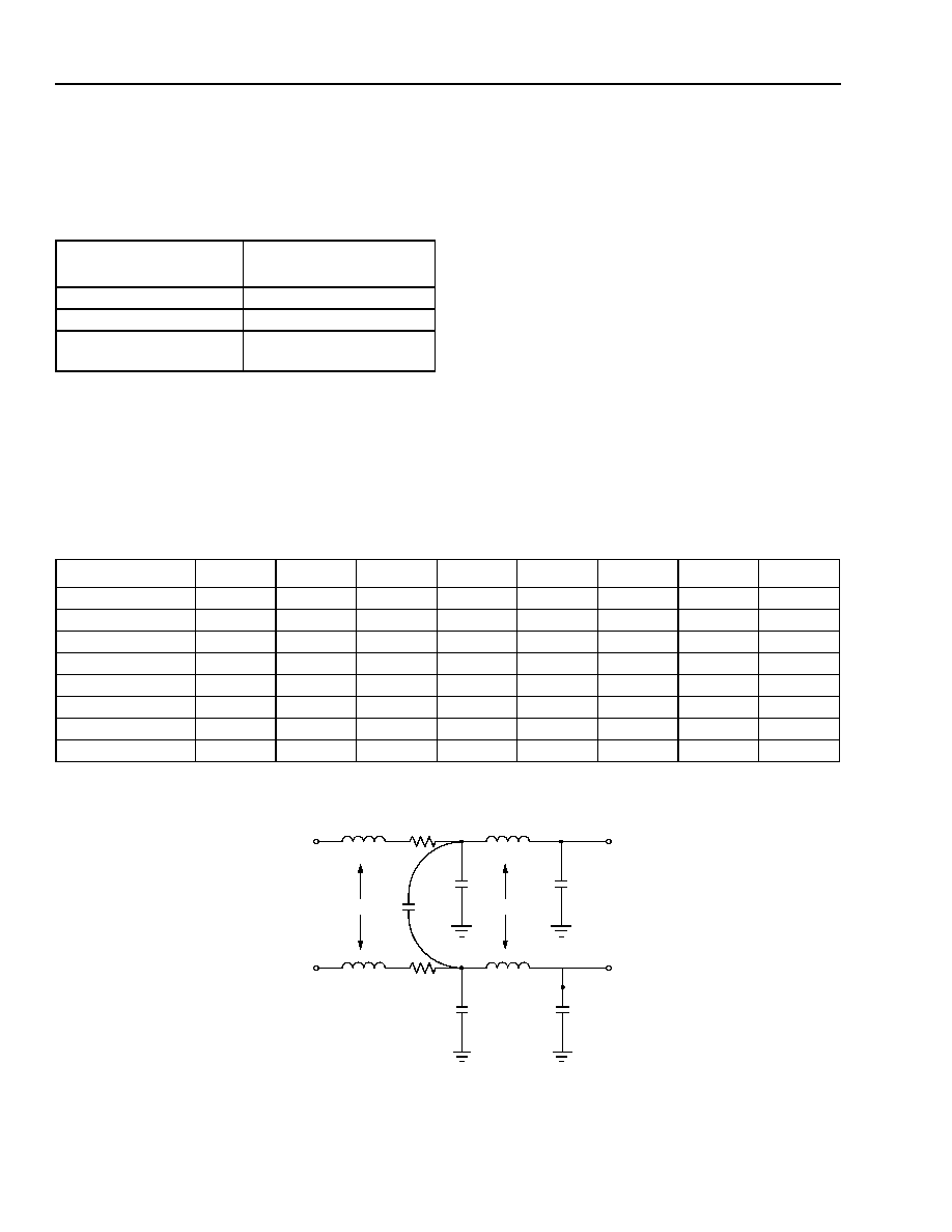
196
196
Lucent Technologies Inc.
Data Sheet
June 1999
ORCA Series 3C and 3T FPGAs
Package Coplanarity
The coplanarity limits of the
ORCA
Series 3 packages
are as follows.
Table 77. Package Coplanarity
Package Parasitics
The electrical performance of an IC package, such as
signal quality and noise sensitivity, is directly affected
by the package parasitics. Table 78 lists eight parasitics
associated with the
ORCA
packages. These parasitics
represent the contributions of all components of a
package, which include the bond wires, all internal
package routing, and the external leads.
Four inductances in nH are listed: L
SW
and L
SL,
the
self-inductance of the lead; and L
MW
and L
ML
, the
mutual inductance to the nearest neighbor lead. These
parameters are important in determining ground
bounce noise and inductive crosstalk noise. Three
capacitances in pF are listed: C
M
, the mutual capaci-
tance of the lead to the nearest neighbor lead; and C
1
and C
2
, the total capacitance of the lead to all other
leads (all other leads are assumed to be grounded).
These parameters are important in determining capaci-
tive crosstalk and the capacitive loading effect of the
lead. The lead resistance value, R
W
, is in M
.
The parasitic values in Table 78 are for the circuit
model of bond wire and package lead parasitics. If the
mutual capacitance value is not used in the designer's
model, then the value listed as mutual capacitance
should be added to each of the C
1
and C
2
capacitors.
Package Type
Coplanarity Limit
(mils)
EBGA
8.0
PBGA
8.0
SQFP/SQFP2
4.0
3.15
Table 78. Package Parasitics
5-3862(F).a
Figure 104. Package Parasitics
Package Type
L
SW
L
MW
R
W
C
1
C
2
C
M
L
SL
L
ML
208-Pin SQFP
4
2
200
1
1
1
7--10
4--6
208-Pin SQFP2
4
2
200
1
1
1
6--9
4--6
240-Pin SQFP
4
2
200
1
1
1
8--12
5--8
240-Pin SQFP2
4
2
200
1
1
1
7--11
4--7
256-Pin PBGA
5
2
220
1
1
1
5--8
2--4
352-Pin PBGA
5
2
220
1.5
1.5
1.5
7--12
3--6
432-Pin EBGA
4
1.5
500
1
1
0.3
3--5.5
0.5--1
600-Pin EBGA
4
1.5
500
1
1
0.4
3--6
0.5--1
PAD N
BOARD PAD
C
M
C
1
L
SW
R
W
L
SL
L
MW
C
2
C
1
L
ML
C
2
PAD N + 1
L
SW
R
W
L
SL

Lucent Technologies Inc.
197
Data Sheet
June 1999
ORCA Series 3C and 3T FPGAs
Package Outline Diagrams
Terms and Definitions
Basic Size (BSC):
The basic size of a dimension is the size from which the limits for that dimension are derived
by the application of the allowance and the tolerance.
Design Size:
The design size of a dimension is the actual size of the design, including an allowance for fit
and tolerance.
Typical (TYP):
When specified after a dimension, this indicates the repeated design size if a tolerance is
specified or repeated basic size if a tolerance is not specified.
Reference (REF):
The reference dimension is an untoleranced dimension used for informational purposes only.
It is a repeated dimension or one that can be derived from other values in the drawing.
Minimum (MIN) or
Maximum (MAX):
Indicates the minimum or maximum allowable size of a dimension.
198
Lucent Technologies Inc.
Data Sheet
June 1999
ORCA Series 3C and 3T FPGAs
Package Outline Diagrams
(continued)
208-Pin SQFP
Dimensions are in millimeters.
Note: The dimensions in this outline diagram are intended for informational purposes only.
For detailed schematics to assist your design efforts, please contact your Lucent Technologies Sales Representative.
156
105
30.60 ± 0.20
157
208
1
52
53
104
28.00 ± 0.20
28.00
± 0.20
30.60
± 0.20
PIN #1 IDENTIFIER ZONE
4.10 MAX
0.08
3.40 ± 0.20
SEATING PLANE
0.25 MIN
0.50 TYP
DETAIL B
DETAIL A
0.50/0.75
GAGE PLANE
SEATING PLANE
1.30 REF
0.25
DETAIL A
DETAIL B
0.17/0.27
0.10
M
0.090/0.200
Lucent Technologies Inc.
199
Data Sheet
June 1999
ORCA Series 3C and 3T FPGAs
Package Outline Diagrams
(continued)
208-Pin SQFP2
Dimensions are in millimeters.
DETAIL C (SQFP2 CHIP-UP)
5-3828(F).a
5-3828(F)
CHIP
CHIP BONDED FACE UP
COPPER HEAT SINK
0.50/0.75
GAGE PLANE
SEATING PLANE
1.30 REF
0.25
DETAIL A
DETAIL B
0.17/0.2
0.10
M
0.090/0.200
156
105
30.60
±
0.20
157
208
53
104
28.00
±
0.20
EXPOSED HEAT SINK APPEARS ON BOTTOM
SURFACE: CHIP BONDED FACE UP. (SEE DETAIL C.)
28.00
±
0.20
30.60
±
0.20
PIN #1 IDENTIFIER ZONE
21.0
REF
21.0 REF
4.10 MAX
0.08
3.40
±
0.20
SEATING PLANE
0.25 MIN
0.50 TYP
DETAIL B
DETAIL A
200
Lucent Technologies Inc.
Data Sheet
June 1999
ORCA Series 3C and 3T FPGAs
Package Outline Diagrams
(continued)
240-Pin SQFP
Dimensions are in millimeters.
Note: The dimensions in this outline diagram are intended for informational purposes only. For detailed schematics to assist your design efforts,
please contact your Lucent Technologies Sales Representative.
0.50/0.75
GAGE PLANE
SEATING PLANE
1.30 REF
0.25
DETAIL A
DETAIL B
0.17/0.27
0.10
M
0.090/0.200
180
121
181
240
34.60 ± 0.20
1
32.00 ± 0.20
60
61
120
PIN #1 IDENTIFIER ZONE
32.00
± 0.20
34.60
± 0.20
0.08
3.40 ± 0.20
SEATING PLANE
0.25 MIN
0.50 TYP
DETAIL A
DETAIL B
4.10 MAX
Lucent Technologies Inc.
201
Data Sheet
June 1999
ORCA Series 3C and 3T FPGAs
Package Outline Diagrams
(continued)
240-Pin SQFP2
Dimensions are in millimeters.
DETAIL C (SQFP2 CHIP-UP)
5-3825(F).a
0.50/0.75
GAGE PLANE
SEATING PLANE
1.30 REF
0.25
DETAIL A
DETAIL B
0.17/0.27
0.10
M
0.090/0.200
CHIP
CHIP BONDED FACE UP
COPPER HEAT SINK
0.08
3.40
±
0.20
SEATING PLANE
0.25 MIN
0.50 TYP
DETAIL A
DETAIL B
180
121
181
240
34.60
±
0.20
1
32.00
±
0.20
60
61
120
PIN #1 IDENTI FIER ZONE
32.00
±
0.20
34.60
±
0.20
EXPOSED HEAT SINK APPEARS ON BOTTOM
SURFACE: CHIP BONDED FACE UP. (SEE DETAIL C.)
24.2
REF
24. 2 REF
4.10 MAX
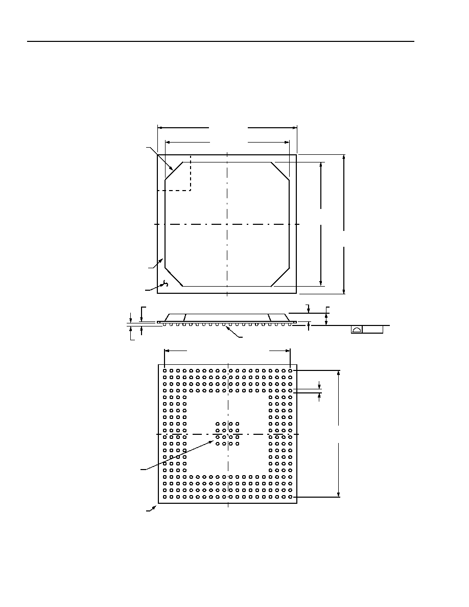
202
Lucent Technologies Inc.
Data Sheet
June 1999
ORCA Series 3C and 3T FPGAs
Package Outline Diagrams
(continued)
256-Pin PBGA
Dimensions are in millimeters.
5-4406(F)
Note: Although the 16 thermal enhancement balls are stated as an option, they are standard on the 256 FPGA package.
0.36
±
0.04
1.17
±
0.05
2.13
±
0.19
SEATING PLANE
SOLDER BALL
0.60
±
0.10
0.20
PWB
MOLD
COMPOUND
27.00
±
0.20
27.00
±
0.20
24.00
+0.70
≠0.00
24.00
+0.70
≠0.00
A1 BALL
IDENTIFIER ZONE
A
B
C
D
E
F
G
H
J
K
L
M
Y
N
P
R
T
U
V
W
1 2 3 4 5 6 7 8 9 10
11
12
13
14
15
16
17
18
20
19
CENTER ARRAY
FOR THERMAL
ENHANCEMENT
(OPTIONAL)
19 SPACES @ 1.27 = 24.13
A1 BALL
CORNER
19 SPACES
@ 1.27 = 24.13
0.75
±
0.15
(SEE NOTE BELOW)
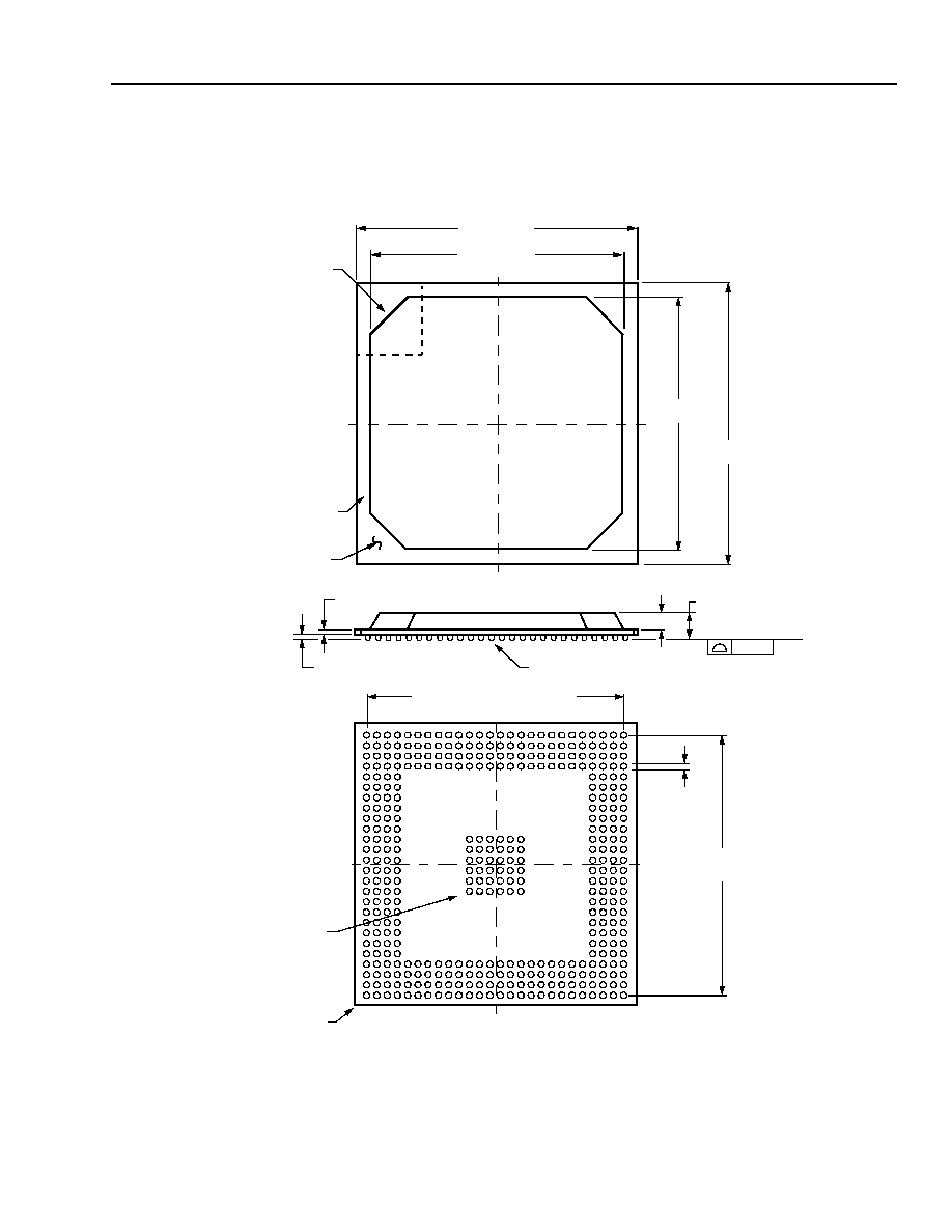
Lucent Technologies Inc.
203
Data Sheet
June 1999
ORCA Series 3C and 3T FPGAs
Package Outline Diagrams
(continued)
352-Pin PBGA
Dimensions are in millimeters.
5-4407(F)
Note: Although the 36 thermal enhancement balls are stated as an option, they are standard on the 352 FPGA package.
0.56
±
0.06
1.17
±
0.05
2.33
±
0.21
SEATING PLANE
SOLDER BALL
0.60
±
0.10
0.20
PWB
MOLD
COMPOUND
35.00
+0.70
≠0.00
30.00
A1 BALL
IDENTIFIER ZONE
AF
AE
AD
AC
AB
AA
Y
W
V
U
T
R
G
25 SPACES @ 1.27 = 31.75
P
N
M
L
K
J
H
1 2 3 4 5 6 7 8 9 10
12
14 16
18
22
24
26
20
11 13
15
17
21
19
23
25
F
E
D
C
B
A
CENTER ARRAY
25 SPACES
A1 BALL
0.75
±
0.15
35.00
±
0.20
30.00
+0.70
≠0.00
±
0.20
@ 1.27 = 31.75
FOR THERMAL
ENHANCEMENT
(OPTIONAL)
CORNER
(SEE NOTE BELOW)
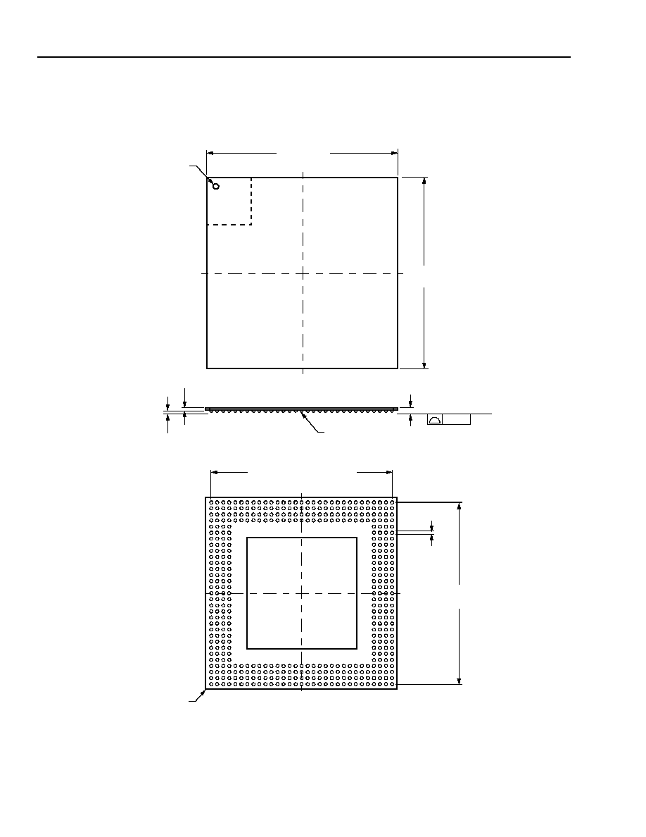
204
Lucent Technologies Inc.
Data Sheet
June 1999
ORCA Series 3C and 3T FPGAs
Package Outline Diagrams
(continued)
432-Pin EBGA
Dimensions are in millimeters.
5-4409(F)
0.91
±
0.06
1.54
±
0.13
SEATING PLANE
SOLDER BALL
0.63
±
0.07
0.20
40.00
±
0.10
40.00
A1 BALL
M
D
AG
B
F
K
H
G
E
AD
L
T
J
N
AJ
C
Y
P
AH
AE
AC
AA
W
U
R
AK
AF
AB
V
AL
A
19
30
26
5
28
24
22
23
25
7
20
31
29
15
21
18
3
27
11
17
4
6
8
10
12
14 16
2
9
13
1
30 SPACES @ 1.27 = 38.10
30 SPACES
A1 BALL
0.75
±
0.15
IDENTIFIER ZONE
±
0.10
@ 1.27 = 38.10
CORNER
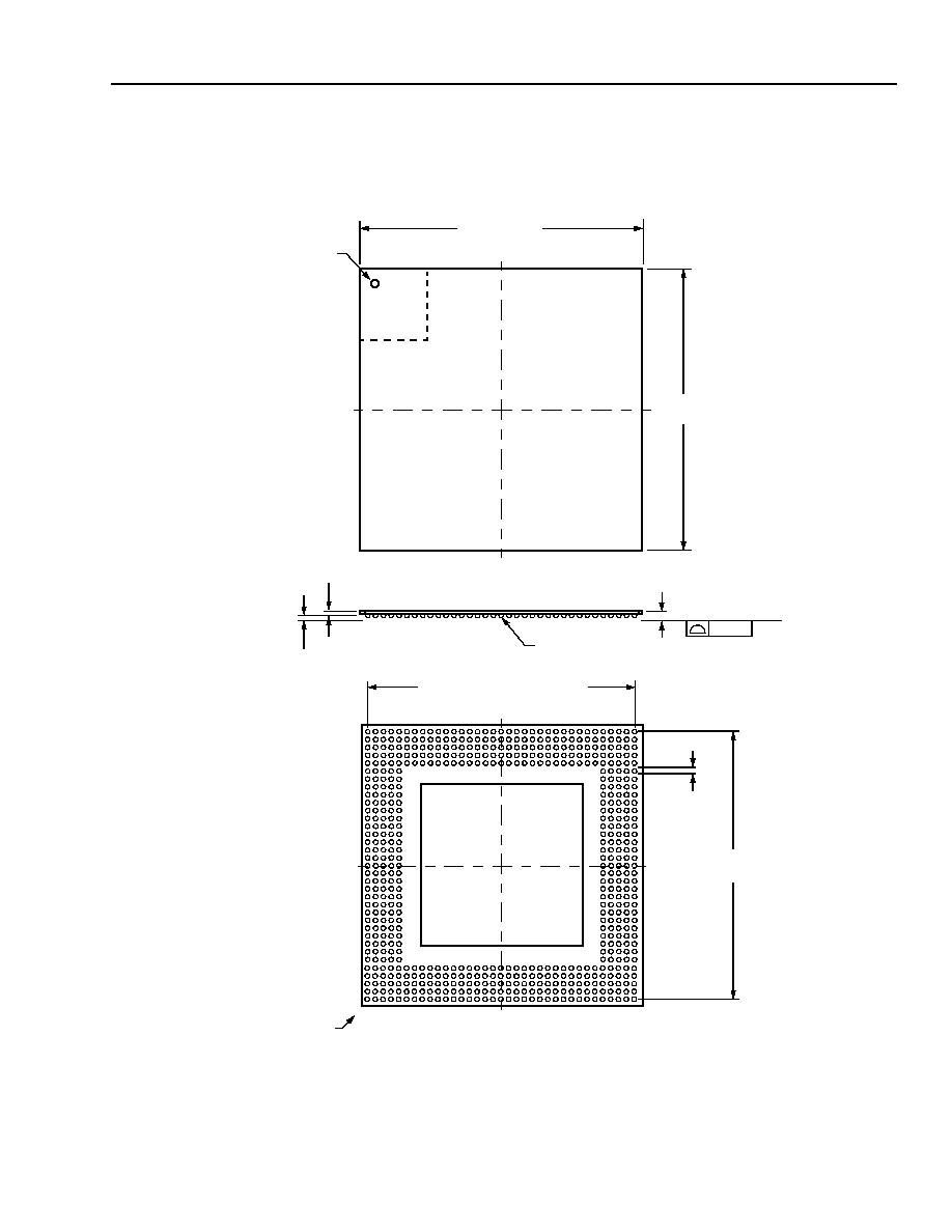
Lucent Technologies Inc.
205
Data Sheet
June 1999
ORCA Series 3C and 3T FPGAs
Package Outline Diagrams
(continued)
600-Pin EBGA
Dimensions are in millimeters.
5-4408(F)
0.91
±
0.06
1.54
±
0.13
SEATING PLANE
SOLDER BALL
0.63
±
0.07
0.20
45.00
±
0.10
45.00
A1 BALL
T
D
H
AL
F
K
B
P
M
L
J
AH
R
C
E
Y
N
U
AN
G
AD
V
AM
AJ
AG
AE
AC
AA
W
AP
AK
AF
AB
AR
A
19
30
26 28
24
32
22
20
18
4
6
8 10 12
14 16
2
34
5
23 25
7
31
29
15
21
3
27
11
17
9
13
1
35
33
34 SPACES @ 1.27 = 43.18
34 SPACES
A1 BALL
0.75
±
0.15
IDENTIFIER ZONE
±
0.10
@ 1.27 = 43.18
CORNER
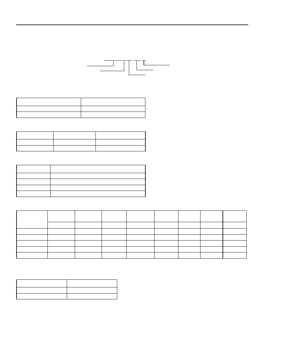
206
Lucent Technologies Inc.
Data Sheet
June 1999
ORCA Series 3C and 3T FPGAs
Ordering Information
OR3C80, -4 Speed Grade, 240-pin Power Quad Shrink Flat Package (SQFP2), Commercial Temperature
Table 79. Voltage Options
Table 80. Temperature Options
Table 81. Package Options
Table 82.
ORCA
Series 3
Package Matrix
Key: C = commercial, I = industrial.
Table 83. Speed Grade Options
Device
Voltage
OR3Cxx
5.0 V
OR3Txxx
3.3 V
Symbol
Description
Temperature
(Blank)
Commercial
0 ∞C to 70 ∞C
I
Industrial
≠40 ∞C to +85 ∞C
Symbol
Description
BA
Plastic Ball Grid Array (PBGA)
BC
Enhanced Ball Grid Array (EBGA)
PS
Power Quad Shrink Flat Package (SQFP2)
S
Shrink Quad Flat Package (SQFP)
Packages
208-Pin
EIAJ SQFP
208-Pin
EIAJ/SQFP2
240-Pin
EIAJ SQFP
240-Pin
EIAJ/SQFP2
256-Pin
PBGA
352-Pin
PBGA
432-Pin
EBGA
600-Pin
EBGA
S208
PS208
S240
PS240
BA256
BA352
BC432
BC600
OR3T20
Cl
--
CI
--
CI
CI
--
--
OR3T30
CI
--
CI
--
CI
CI
--
--
OR3C/T55
--
CI
--
CI
CI
CI
--
--
OR3C/T80
--
CI
--
CI
--
CI
CI
--
OR3T125
--
CI
--
CI
--
CI
CI
CI
Device
Speed Grade
OR3Cxx
-4, -5
OR3Txxx
-5, -6, -7
OR3C80-4 PS 240
DEVICE TYPE
SPEED GRADE
PACKAGE TYPE
NUMBER OF PINS
TEMPERATURE RANGE
Example:

Lucent Technologies Inc.
207
Data Sheet
June 1999
ORCA Series 3C and 3T FPGAs
Index
A
Absolute Maximum Ratings, 96
AND-OR-INVERT (AOI), 6
AND-OR-INVERT (AOI),1
(see also Supplemental Logic
Interconnect Cell (SLIC), 1
Architecture
Overview, 6--9
ASWE, 9, 11, 15--17, 23, 33, 48
B
Bidirectional Buffers (BIDIs), 6, 19, 43, 83
(see also Routingand SLIC)
Bit Stream (see FPGA Configuration)
Bit Stream Error Checking, 88
(see also FPGA states of Operation)
Boundary Scan, 55
(see Special Function Blocks)
C
Clock Control (CLKCNTRL), 50
(see also Clock Distribution Network and
Special Function Blocks)
Clock Distribution Network, 48≠51
CLKCNTRL, 50
ExpressCLK, 48
Inputs, 51
Fast Clock, 48, 51
Global Control Signals, 48
In the PICs
ExpressCLK, 50
System Clock, 50
In the PLC Array
Fast Clock, 49
System Clock, 49
PFU Clock Sources, 48
Selecting Clock Input Pins, 51
System Clock, 48
To the PLC Array
Fast Clock, 50
System Clock, 50
Clock Enable (CE), 9, 11, 17, 23, 31, 48
Clock Multiplication (see PCM)
Comparator (see LUT Operating Modes)
Configuration (see FPGA States of Operation
or FPGA Configuration)
Control Inputs (see PICs, Inputs)
D
Demultiplexing (see PICs, Input Demultiplexing), 38
Duty-Cycle Adjustment (see PCM)
E
Electrical Characteristics, 97, 98
Error Checking (see FPGA Configuration)
ExpressCLK, 1, 6, 31, 34, 37, 39, 41, 43, 47--51,
70--74, 77--81
(see also Clock distribution Network and
Programmable Clock Manager)
F
Fast Clock, 46--51, 54
(see Clock Distribution Network)
5 V Tolerant I/O 35
Flexible Input Structure (FINS) 1, 27, 32
(see also Routing)
FPGA Configuration, 87--94
Configuration Frame Format, 87
Configuration Modes, 89
Asynchronous Peripheral Mode, 91
Daisy-Chaining, 95
Master Parallel Mode, 89
Master Serial Mode, 90
Microprocessor Interface (MPI) Mode, 91
Slave Parallel Mode, 94
Slave Serial Mode, 94
Data Format, 86
Data Frame, 86
Using
ORCA
Foundry to Generate RAM Data, 86
FPGA States of Operation
Configuration, 83
Initialization, 82
Other Configuration Options, 85
Partial Reconfiguration, 85
Reconfiguration, 85
Start-Up, 84
I
IEEE
Standard, 1149.1 55, 59
Initialization (see FPGA States of Operation)
Input/Output Buffers
Measurement Conditions, 138
Output Buffer Characteristics
OR3Cxx, 139
OR3Txxx, 141
J
JTAG (see Boundry Scan)

208
208
Lucent Technologies Inc.
Data Sheet
June 1999
ORCA Series 3C and 3T FPGAs
Index
(continued)
L
Look-Up Table (LUT) Operating Modes, 11--18
Adder-Subtractor Submode, 15
Counter Submode, 15
Equality Comparators, 16
Half-Logic Mode, 14
Logic Mode, 12
Memory Mode, 17
Multiplier Submode, 16
Ripple Mode, 14
LSR, 11, 17, 23--24, 31, 48
M
Maximum Ratings (see Absolute Maximum Ratings)
Microprocessor Interface (MPI), 62--69
i960
System, 64
Interface to FPGA, 65
PowerPC
System, 63
Setup and Control Registers, 66
Multiplexing (see Output Multiplexing)
Multiplier (see LUT Operating Modes)
O
ORCA
Foundry Development System, 25
Overview, 7
Ordering Information
Package Matrix, 207
Package Options, 207
Temperature Options, 207
Voltage Options, 207
Output (see PICs)
Output Multiplexing, 39
P
Package Information, 200--206
Package Matrix, 204
Package Outline Diagrams, 200
208-Pin SQFP2, 199
240-Pin SQFP2, 202
256-Pin PBGA, 203
352-Pin PBGA, 204
432-Pin EBGA, 205
600-Pin EBGA, 206
Terms and Definitions, 200
PAL
, 1 (see also Supplemental Logic and
Interconnect Cell (SLIC)) 1
PIC Routing (see Routing)
Pin Information
208-Pin SQFP2 Pinout, 151
240-Pin SQFP2 Pinout, 156
256-Pin PBGA Pinout, 162
352-Pin PBGA Pinout, 165
432-Pin EBGA Pinout, 177
600-Pin EBGA Pinout, 184
Package Compatibility, 152
Pin Descriptions 147, 151
Power Dissipation, 144
5 V Tolerant I/O, 143
OR3Cxx, 144
OR3Txxx, 145
PowerPC
(see Microprocessor Interface)
Programmable Clock Manager (PCM), 6, 81
Clock Delay, 74
Clock Multiplication, 75
DLL Mode, 73
PCM Cautions, 81
PCM Detailed Programming, 77
PCM Operation, 76
PCM/FPGA Internal Interface, 76
PLL Mode, 74
Registers, 71
Programmable Function Unit (PFU), 9
Cintrol Inputs, 11
Operating Modes, 11
Softwired LUTs (SWL), 12
Twin-quad Architecture, 1, 8, 14, 19
Programmable Input/Output Cells (PICs), 34--44
5 V Tolerant I/O, 35
Architecture, 43
Control Inputs, 11, 23
ASWE, 11
CE, 11
CLK, 11
GSRN, 11, 24
LSR, 11
SEL, 11
Input Demultiplexing, 38
Inputs, 36
Output Multiplexing, 39
Outputs, 39
Open-Drain Output Option, 39
Propagation Delays, 39
Overview, 32
PIO, 34
PIO Logic, 41
PIO Options, 35
PIO Register Control Signals, 41
Zero-Hold Input, 37
Programmable Logic Cells (PLCs), 9--33
Architecture, 32
Latches/Flip-Flops, 23, 24
PFU, 9
Propagation Delays (see PICs, Outputs)
Routing, 25
SLIC, 19--22

Lucent Technologies Inc.
209
Data Sheet
June 1999
ORCA Series 3C and 3T FPGAs
Index
(continued)
R
RAM (see also FPGA Configuration), 85
Dual-port, 3, 10, 17
Single-port, 3, 10, 17
Recommended Operating Conditions, 95
Reconfiguration (see FPGA States of Operation)
Routing
3-Statable Bidirectional Buffers, 24
BIDI Routing, 24, 27
Clock (and Global CE and LSR) Routing, 30
Configurable Interconnect Points (CIPs), 24
Control Signal and Fast-Carry Routing, 27
Flexible Input Structure (FINS), 26
Inter-PLC Routing Resources, 28
Interquad Routing, 44
Intra-PLC Routing Resources, 26--27
Minimizing Routing Delay, 30
Overview, 5
PFU Output Switching, 26
PIC Routing, 41--43
PIC Interquad (MID) Routing, 46
PLC Routing, 26--32
Programmable Corner Cell Routing, 45
SLIC Connectivity, 27
Switching Routing Segments (xSW), 26
S
SEL, 8, 10, 22
Softwired LUTs (SWLs),1, 6, 11, 12
(see also Look-Up Table Operating Modes)
Special Function Blocks
Boundary Scan, 60
Boundary-Scan Cells, 59
Boundary-Scan Timing, 60
Microprocessor Interface (MPI), 61--68
Programmable Clock Manager (PCM), 69--80
Single Function Blocks, 51
Clock Control (CLKCNTRL), 53
Global 3-State Control (TS_ALL), 52
Global Set/Reset (GSRN), 52
Internal Oscillator, 52
Readback Logic, 51
Start-Up Logic, 53
Start-Up (see FPGA States of Operation)
StopCLK, 1, 5, 53
(see also Special Function Blocks)
Subtractor (see LUT Operating Modes)
Supplemental Logic and Interconnect Cell (SLIC), 1,
18--21
System Clock (see Clock Distribution Network), 47
3-state, 3--4, 17--18, 34, 38, 45--46, 52, 56, 59, 82, 84
T
Timing Characteristics
Asynchronous Peripheral Configuration Mode, 132
Boundry-Scan Timing, 119
Clock Timing, 119
Derating, 98
Description, 98
General Configuration Mode Timing, 129, 130
Master Parallel Configuration Mode, 131
Master Serial Configuration Mode, 130
Microprocessor Interface Configuration Timing, 137
PFU Timing, 100
PIO Timing, 108, 109, 110
PLC Timing, 107
Programmable Clock Manager Timing, 115
Readback Timing, 139
Slave Parallel Configuration Mode, 134
Slave Serial Configuration Mode, 133
SLIC Timing, 107
Tolerant I/O (see 5 V Tolerant I/O), 34
TS_ALL, 52 Twin-quad Architecture (see PFU), 1
U--Z
Zero-hold Inputs, 34--36

Lucent Technologies Inc. reserves the right to make changes to the product(s) or information contained herein without notice. No liability is assumed as a result of their use or application. No rights under any patent
accompany the sale of any such product(s) or information.
ORCA is a registered trademark of Lucent Technologies Inc. Foundry is a trademark of Xilinx, Inc.
Copyright © 1999 Lucent Technologies Inc.
All Rights Reserved
Printed in U.S.A.
June 1999
DS99-087FPGA (Replaces DS98-163FPGA-01)
For additional information, contact your Microelectronics Group Account Manager or the following:
INTERNET:
http://www.lucent.com/micro, or for FPGA information, http://www.lucent.com/orca
E-MAIL:
docmaster@micro.lucent.com
N. AMERICA:
Microelectronics Group, Lucent Technologies Inc., 555 Union Boulevard, Room 30L-15P-BA, Allentown, PA 18103
1-800-372-2447, FAX 610-712-4106 (In CANADA: 1-800-553-2448, FAX 610-712-4106)
ASIA PACIFIC: Microelectronics Group, Lucent Technologies Singapore Pte. Ltd., 77 Science Park Drive, #03-18 Cintech III, Singapore 118256
Tel. (65) 778 8833, FAX (65) 777 7495
CHINA:
Microelectronics Group, Lucent Technologies (China) Co., Ltd., A-F2, 23/F, Zao Fong Universe Building, 1800 Zhong Shan Xi Road
Shanghai 200233 P. R. China Tel. (86) 21 6440 0468, ext. 316, FAX (86) 21 6440 0652
JAPAN:
Microelectronics Group, Lucent Technologies Japan Ltd., 7-18, Higashi-Gotanda 2-chome, Shinagawa-ku, Tokyo 141, Japan
Tel. (81) 3 5421 1600, FAX (81) 3 5421 1700
EUROPE:
Data Requests: MICROELECTRONICS GROUP DATALINE: Tel. (44) 7000 582 368, FAX (44) 1189 328 148
Technical Inquiries: GERMANY: (49) 89 95086 0 (Munich), UNITED KINGDOM: (44) 1344 865 900 (Ascot),
FRANCE: (33) 1 40 83 68 00 (Paris), SWEDEN: (46) 8 594 607 00 (Stockholm), FINLAND: (358) 9 4354 2800 (Helsinki), ITALY: (39) 02
6608131 (Milan), SPAIN: (34) 1 807 1441 (Madrid)