 | –≠–ª–µ–∫—Ç—Ä–æ–Ω–Ω—ã–π –∫–æ–º–ø–æ–Ω–µ–Ω—Ç: ORCAR2 | –°–∫–∞—á–∞—Ç—å:  PDF PDF  ZIP ZIP |

Product Brief
April 1999
TLIU04C1 Quad T1/E1 Line Interface
Features
s
Selectable microprocessor or direct
logic control modes.
s
Quad T1/E1 line interface.
s
Hardware and software reset options.
s
3-state outputs.
s
0.35 µm CMOS technology.
s
Compliant with:
AT&T
CB119 (10/79)
Bellcore
TR-54016 (89)
TR-TSY-000170 (10/97)
TR-TSY-000009 (5/86)
GR-499-CORE (12/95)
GR-253-CORE (12/95)
ANSI
T1.102 (93)
T1.231 (93)
T1.403 (95)
ITU-T
G.703 (88)
G.704 (91)
G.706 (91)
G.732 (88)
G.735-9 (88)
G.775 (11/94)
G.823-4 (3/93)
G.826 (11/93)
I.431 (3/93)
ETSI
TBR 12 (12/93)
TBR 13 (1/96)
s
≠40 ∞C to +85 ∞C operating temperature range.
s
Fine-pitch (25 mil spacing) surface-mount pack-
age, 100-pin BQFP.
s
Transmitter includes transmit encoder (B8ZS or
HDB3), pulse shaping, and line driver.
s
Five pulse equalization settings for template com-
pliance at DSX cross connect.
s
Receive includes equalization, digital clock and
data recovery (immune to false lock), and receive
decoder (B8ZS or HDB3).
s
CEPT/E1 interference immunity as required by
G.703.
s
Transmit jitter <0.02 UI.
s
Receive generated jitter <0.05 UI.
s
Jitter attenuator selectable for use in transmit or
receive path. Jitter attenuation characteristics are
data pattern independent.
s
For use with 100
DS1 twisted-pair, 120
E1
twisted-pair, and 75
E1 coaxial cable.
s
Common part available for transmit/receive
transformers.
s
Analog LOS alarm for signals less than ≠18 dB for
greater than 1 ms or 10 bit symbol periods to
255 bit symbol periods (selectable).
s
Digital LOS alarm for 100 zeros (DS1) or 255 zeros
(CEPT).
s
Diagnostic loopback modes.
s
Low power consumption.
Applications
s
T1/E1 network performance monitoring
s
SONET/SDH multiplexers
s
Asynchronous multiplexers (M13)
s
Digital access cross connects (DACs)
s
Channel banks
s
Digital radio base stations, remote wireless mod-
ules
s
PBX interface
2
2
Agere Systems Inc.
Product Brief
April 1999
TLIU04C1 Quad T1/E1 Line Interface
5-7823(F)
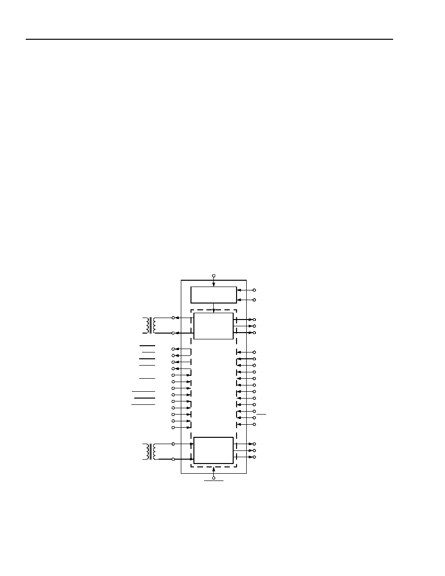
Note: CMODE pin not shown.
Figure 1. TLIU04C1 Block Diagram, CMODE = 0 (Direct Logic Mode)
TTIP[1--4]
TRING[1--4]
QUAD
LINE
INTERFACE
UNIT
RTIP[1--4]
RRING[1--4]
QUAD
TRANSMIT
SECTION
QUAD
RECEIVE
SECTION
RESET
CLOCK
MULTIPLIER
XCLK
LOTC[1--4]
TDM[1--4]
DLOS[1--4]
ALOS[1--4]
XAIS[1--4]
ALMT[1--4]
PWRDN[1--4]
FLLOOP[1--4]
RLOOP[1--4]
EQA[1--4]
EQB[1--4]
EQC[1--4]
CLKS
CLKM
TCLK[1--4]
TPD[1--4]
ACM
ALM
DUAL
JAT
JAR
JABW0
RCVAIS
LOSSTD
LOSSD
ICT
LOXC
RCLK[1--4]
RND[1--4]
RPD[1--4]
ALTIMER
TND[1--4]
DLLOOP[1--4]
Description
The TLIU04C1 is a quad line interface containing four
line transmit and receive channels for use in both North
American (T1/DS1) and European (E1/CEPT) applica-
tions. The line interface unit has the same functions as
the Agere T7698.
The device can operate in either of two modes, chosen
by the logic state of a control pin. The block diagrams
of the direct logic and microprocessor modes are
shown in Figure 1 and Figure 2, respectively. A direct
logic control mode provides the ability to define the
architecture, initiate loopbacks, and monitor alarms
without connecting to a microprocessor by setting the
logic levels on control pins. The microprocessor mode
uses a parallel microprocessor interface to allow the
user to configure the device. The interface is compati-
ble with many commercially available microprocessors.
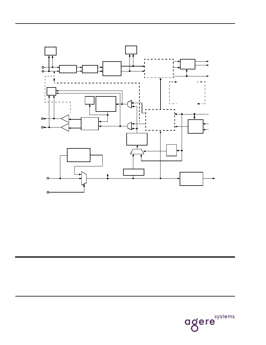
The block diagram of the quad LIU for a single channel
is shown in Figure 3. The line receiver performs clock
and data recovery using a fully integrated digital phase-
locked loop.
This digital implementation prevents false lock condi-
tions that are common when recovering sparse data
patterns with analog phase-locked loops.
Equalization circuitry in the receiver provides a high
level of interference immunity. As an option, the raw
sliced data (no retiming) can be output on the receive
data pins. Transmit equalization is implemented with
low-impedance output drivers that provide shaped
waveforms to the transformer, guaranteeing template
conformance.
The quad device will interface to the digital cross con-
nect (DSX) at lengths of up to 655 ft. for DS1 operation,
or to line impedances of 75
or 120
for CEPT oper-
ation. A selectable jitter attenuator may be placed in
the receive signal path for low-bandwidth line-synchro-
nous applications, or it may be placed in the transmit
path for multiplexer applications where DS1/CEPT sig-
nals are demultiplexed from higher rate signals. The jit-
ter attenuator will perform the clock smoothing required
on the resulting demultiplexed gapped clock.

Agere Systems Inc.
3
Product Brief
April 1999
TLIU04C1 Quad T1/E1 Line Interface
Description
(continued)
5-7822(F).a
Note: CMODE pin not shown.
Figure 2. TLIU04C1 Block Diagram, CMODE = 1 (Microprocessor Mode)
TTIP[1--4]
TRING[1--4]
ICT
LOXC
QUAD
LINE
INTERFACE
UNIT
RTIP[1--4]
RRING[1--4]
QUAD
TRANSMIT
SECTION
QUAD
RECEIVE
SECTION
RESET
4
4
4
CLKS
4
4
4
MICRO-
INTERFACE
PROCESSOR
A[3:0]
AD[7:0]
RDY_DTACK
INT
WR_DS
ALE_AS
CS
MPMUX
MPMODE
MPCLK
RCLK[1--4]
RND[1--4]
RPD[1--4]
TPD[1--4]
TND[1--4]
TCLK[1--4]
CLOCK
MULTIPLIER
CLKM
XCLK
RD_RW
Copyright © 2002 Agere Systems Inc.
All Rights Reserved
April 1999
PN99-074T1E1
For additional information, contact your Agere Systems Account Manager or the following:
INTERNET:
http://www.agere.com
E-MAIL:
docmaster@agere.com
N. AMERICA:
Agere Systems Inc., 555 Union Boulevard, Room 30L-15P-BA, Allentown, PA 18109-3286
1-800-372-2447, FAX 610-712-4106 (In CANADA: 1-800-553-2448, FAX 610-712-4106)
ASIA:
Agere Systems Hong Kong Ltd., Suites 3201 & 3210-12, 32/F, Tower 2, The Gateway, Harbour City, Kowloon
Tel. (852) 3129-2000, FAX (852) 3129-2020
CHINA: (86) 21-5047-1212 (Shanghai), (86) 10-6522-5566 (Beijing), (86) 755-695-7224 (Shenzhen)
JAPAN: (81) 3-5421-1600 (Tokyo), KOREA: (82) 2-767-1850 (Seoul), SINGAPORE: (65) 6778-8833, TAIWAN: (886) 2-2725-5858 (Taipei)
EUROPE:
Tel. (44) 7000 624624, FAX (44) 1344 488 045
Product Brief
April 1999
TLIU04C1 Quad T1/E1 Line Interface
Agere Systems Inc. reserves the right to make changes to the product(s) or information contained herein without notice. No liability is assumed as a result of their use or application.
Agere, Agere Systems, and the Agere logo are trademarks of Agere Systems Inc.
Description
(continued)
5-4556(F).er.3
Figure 3. Block Diagram of the Quad LIU (Single Channel)
RTIP[1--4]
RRING[1--4]
FLLOOP
(NO LIU AIS)
EQUALIZER
SLICERS
CLOCK AND
DATA
RECOVERY
DLOS
RND[1--4]
RPD[1--4]
RCLK[1--4]
DECODER
DLLOOP
RLOOP
TCLK[1--4]
TND[1--4]
JITTER
(RECEIVE PATH)
TPD[1--4]
FLLOOP
(DURING LIU AIS)
PULSE-
WIDTH
CONTROLLER
TDM
LOTC
PULSE
EQUALIZER
TRANSMIT
DRIVER
TTIP[1--4]
TRING[1--4]
LOSS OF
XCLK
MONITOR
DIVIDE BY 16
ALARM
SIGNAL (AIS)
ENCODER
ALOS
INDICATION
ATTENUATOR
JITTER
(TRANSMIT PATH)
ATTENUATOR
(CLOCK)
(DATA)
LOSS
OF
TCLK
LOXC
XCLK
16x
CLOCK
MULTIPLIER
CLKS
INTXCLK