 | –≠–ª–µ–∫—Ç—Ä–æ–Ω–Ω—ã–π –∫–æ–º–ø–æ–Ω–µ–Ω—Ç: ORLI10G | –°–∫–∞—á–∞—Ç—å:  PDF PDF  ZIP ZIP |
Data Sheet
October 2001
ORCA
Æ
ORLI10G Quad 2.5 Gbits/s
10 Gbits/s, and 12.5 Gbits/s Line Interface FPSC
Introduction
Agere Systems Inc. has developed a new ORCA
Series 4 based FPSC which combines a high-speed
line interface with a flexible FPGA logic core. Built on
the Series 4 reconfigurable embedded system-on-
chips (SoC) architecture, the ORLI10G consists of an
OIF standard (OIF 99.102.5) compliant XSBI or
OIF-SFI4-01.0 SFI-4, 10 Gbits/s or 12.5 Gbits/s
transmit and 10 Gbits/s or 12.5 Gbits/s receive line
interface. Both transmit and receive interfaces con-
sist of 16-bit LVDS data up to 850 Mbits/s, integrated
transmit and receive programmable PLLs for data
rate conversions between the line-side and system-
side data rates, and a programmable logic interface
at the system end for use with SONET/SDH, Ether-
net, or OTN/digital wrapper with strong FEC system
device data standards. In addition to the embedded
functionality, the device will include up to 400k of
usable FPGA gates. The line interface includes logic
to divide the data rate down to 212 MHz or less
(1/4 line rate) or 106 MHz or less (1/8 line rate) for
transfer to the FPGA logic. The ORLI10G is designed
to connect directly to Agere's 10 Gbits/s TTRN0110G
MUX and TRCV0110G deMUX or Agere's
12.5 Gbits/s TTRN0126 MUX and TRCV01126
deMUX on the line side, as well as other industry-
standard devices. The programmable logic interface
on the system side allows for direct connection to a
10 Gbits/s Ethernet MAC, a 10 Gbits/s SONET/SDH
framer/data engine, or a 10 Gbits/s/12.5 Gbits/s digi-
tal wrapper/FEC framer/data engine.
For 10 Gbits/s Ethernet, the ORLI10G supports the
physical coding sublayer (PCS), interfaces to the
physical media attachment (PMA), and connects to
the system interface (host or switch) for the proposed
IEEE
Æ
802.3ae 10 Gbits/s serial LAN PHY.
The ORLI10G FPSC is a high-speed programmable
device for 10G/s data solutions. It can be used as the
interface between the line interface and the system
interface in a variety of emerging networks, including
10 Gbits/s SONET/SDH (OC-192/STM-48),
10 Gbits/s optical transport networks (OTN) using
digital wrapper and strong FEC, or 10 Gbits/s Ether-
net. Other functions include use in Quad OC-48/
STM-16 SONET/SDH systems, interfaces between
Quad OC-48/STM-16 and OC-192/STM-64 compo-
nents, and use as a generic data transfer mechanism
between two devices at 10 Gbits/s rates. Data is
received at the line interface and then sent to either a
4-bit or 8-bit serial-to-parallel converter. On the trans-
mit interface, either a 4-bit or 8-bit parallel-to-serial
converter is used. Thus, the data rate at the internal
FPGA interface is either 1/4 or 1/8 the line rate.
The programmable PLLs on the ORLI10G provide for
great flexibility in handling clock rate conversion due
to differing amounts of overhead bits in various sys-
tem data standards. For example, the ORLI10G can
divide down the STS-192/STM-64 SONET/SDH data
line rate of 622 MHz by 4 to synchronize with a
155 MHz system clock, or the 12.5 Gbits/s Super-
FEC data line rate of 781 MHz can be divided by 8 to
98 MHz system clock or by 8 x 4/5 to provide a
78 MHz system data rate.
Table 1. ORCA ORLI10G--Available FPGA Logic
* 192 user I/Os for the 416 PBGAM package and 316 user I/Os for the 680 PBGAM package are available out of the 432 possible user
I/Os.
Note: The embedded core and interface are not included in the above gate counts. The usable gate counts range from a logic-only gate
count to a gate count assuming 20% of the PFUs/SLICs being used as RAMs. The logic-only gate count includes each PFU/SLIC
(counted as 108 gates/PFU), including 12 gates per LUT/FF pair (eight per PFU), and 12 gates per SLIC/FF pair (one per PFU).
Each of the four PIO groups are counted as 16 gates (three FFs, fast-capture latch, output logic, CLK, and I/O buffers). PFUs used
as RAM are counted at four gates per bit, with each PFU capable of implementing a 32 x 4 RAM (or 512 gates) per PFU. Embedded
block RAM (EBR) is counted as four gates per bit, plus each block has an additional 25k gates. 7k gates are used for each PLL and
50k gates for the embedded system bus and microprocessor interface logic. Both the EBR and PLLs are conservatively utilized in
the gate count calculations.
Device
PFU
Rows
PFU
Columns
Total
PFUs
User I/Os*
LUTs
EBR
Blocks
EBR Bits
(k)
Usable
Gates (k)
ORLI10G
36
36
1296
432
10,368
12
111
380--800

Table of Contents
Contents
Page
Contents
Page
2
Agere Systems Inc.
Data Sheet
October 2001
10 Gbits/s, and 12.5 Gbits/s Line Interface FPSC
ORCA ORLI10G Quad 2.5 Gbits/s
Introduction..................................................................1
Embedded Function Features .....................................4
Intellectual Property Features......................................4
Programmable Features..............................................4
Programmable Logic System Features .......................6
Description...................................................................7
FPSC Definition ........................................................7
FPSC Overview ........................................................7
FPSC Gate Counting ................................................7
FPGA/Embedded Core Interface ..............................7
ORCA Foundry Development System ......................7
FPSC Design Kit .......................................................8
FPGA Logic Overview...............................................8
PLC Logic .................................................................8
Programmable I/O.....................................................9
Routing......................................................................9
System-Level Features..............................................10
Microprocessor Interface ........................................10
System Bus.............................................................10
Phase-Locked Loops ..............................................10
Embedded Block RAM ............................................10
Configuration...........................................................11
Additional Information .............................................11
ORLI10G Overview ...................................................11
Device Layout .........................................................11
10G Mode ...............................................................11
2.5G Mode ..............................................................12
Receive Path Details .................................................15
Line Interface ..........................................................15
DeMUX ...................................................................15
Onboard Receive PLLs...........................................15
Transmit Path Details ................................................17
MUX ........................................................................17
Onboard Transmit PLLs..........................................17
Line Interface ..........................................................17
ORLI10G Demultiplexer (Rx) Detail ..........................19
ORLI10G Multiplexer (Tx) Detail ...............................25
ORLI10G Embedded PLLs........................................31
ORLI10G Embedded Programmable PLLs
Specifications ........................................................... 32
ORLI10G Reset Requirements................................. 32
Line Interface Circuit Specifications ......................... 33
Power Supply Decoupling LC Circuit ..................... 33
XGMII ORCA 4E Receive Analysis .......................... 34
XGMII Considerations ............................................ 34
Absolute Maximum Ratings...................................... 35
Recommended Operating Conditions ...................... 35
Embedded Core LVDS I/O ....................................... 36
LVDS Receiver Buffer Requirements..................... 37
Timing Characteristics .............................................. 38
Receive Input Data Interface.................................. 38
Transmit STS-48/STS-192 (2.5G/10G) Data
Outputs ..................................................................... 39
Input/Output Buffer Measurement Conditions
(Non-LVDS Buffer) ................................................... 40
LVDS Buffer Characteristics..................................... 41
Termination Resistor .............................................. 41
LVDS Driver Buffer Capabilities ............................. 41
Pin Information ......................................................... 42
Package Pinouts .................................................... 47
Package Thermal Characteristics Summary ............ 65
JA ........................................................................ 65
JC ........................................................................ 65
JC ........................................................................ 65
JB ........................................................................ 65
FPSC Maximum Junction Temperature ................. 65
Package Thermal Characteristics............................. 66
Heat Sink Vendors for BGA Packages ..................... 66
Package Coplanarity ................................................ 66
Package Parasitics ................................................... 67
Package Outline Diagrams....................................... 68
Terms and Definitions ............................................ 68
416-Pin PBGAM..................................................... 69
680-Pin PBGAM..................................................... 70
Hardware Ordering Information ................................ 71
Software Ordering Information ................................. 71

Agere Systems Inc.
3
Data Sheet
October 2001
Table of Contents
(continued)
List of Figures
Page
List of Tables
Page
10 Gbits/s, and 12.5 Gbits/s Line Interface FPSC
ORCA ORLI10G Quad 2.5 Gbits/s
Figure 1. ORCA ORLI10G Block Diagram ...............13
Figure 2. 10G (Single-Channel) and 2.5G
(Quad-Channel) Modes .........................................14
Figure 3. ORLI10G Embedded Core Receive
Path Diagram .........................................................16
Figure 4. ORLI10G Embedded Core Transmit Path
Diagram .................................................................18
Figure 5. Demultiplexer Output Data Structure ........20
Figure 6. Demultiplexer Serial-to-Parallel
Conversion--Divide by 8, 10G Mode .....................21
Figure 7. Demultiplexer Serial-to-Parallel
Conversion--Divide by 4, 10G Mode .....................22
Figure 8. Demultiplexer Serial-to-Parallel
Conversion--Divide by 8, 2.5G Mode ....................23
Figure 9. Demultiplexer Serial-to-Parallel
Conversion--Divide by 4, 2.5G Mode ....................24
Figure 10. Multiplexer Input Data Structure ..............26
Figure 11. Multiplexer Parallel-to-Serial
Conversion--Divide by 8, 10G Mode .....................27
Figure 12. Multiplexer Parallel-to-Serial
Conversion--Divide by 4, 10G Mode .....................28
Figure 13. Multiplexer Parallel-to-Serial
Conversion--Divide by 8, 2.5G Mode ....................29
Figure 14. Multiplexer Parallel-to-Serial
Conversion--Divide by 4, 2.5G Mode ....................30
Figure 15. ORLI10G Programmable PLL Block
Diagram .................................................................31
Figure 16. Sample Power Supply Filter Network for
Analog LI Power Supply Pins .................................33
Figure 17. Simplified XGMII Block Diagram .............34
Figure 18. Receive Input Data Timing ......................38
Figure 19. Transmit Output Data Timing ..................39
Figure 20. ac Test Loads ..........................................40
Figure 21. Output Buffer Delays ...............................40
Figure 22. Input Buffer Delays ..................................40
Figure 23. LVDS Driver and Receiver and Associated
Internal Components ..............................................41
Figure 24. LVDS Driver and Receiver ......................41
Figure 25. LVDS Driver ............................................41
Figure 26. Package Parasitics ..................................67
Table 1. ORCA ORLI10G--Available FPGA Logic ... 1
Table 2. Programmable PLL Specifications ............ 32
Table 3. ORLI10G Reset Requirements .................. 32
Table 4. HSTL Input Requirements to FPGA .......... 35
Table 5. Absolute Maximum Ratings ....................... 35
Table 6. Recommended Operating Conditions ....... 35
Table 7. Driver dc Data ............................................ 36
Table 8. Driver ac Data ............................................ 36
Table 9. Driver Power Consumption ........................ 36
Table 10. Receiver ac Data ..................................... 37
Table 11. Receiver Power Consumption ................. 37
Table 12. Receiver dc Data ..................................... 37
Table 13. LVDS Operating Parameters ................... 37
Table 14. Receive Data Input Timing ...................... 38
Table 15. Transmit Data Output Timing .................. 39
Table 16. FPGA Common-Function Pin
Description ............................................................ 42
Table 17. FPSC Function Pin Description ............... 45
Table 18. Embedded Core/FPGA Interface Signal
Description ............................................................ 46
Table 19. ORCA Programmable I/Os Summary ...... 47
Table 20. PBGA Pinout Table ................................. 48
Table 21. ORCA ORLI10G Plastic Package
Thermal Guidelines ............................................... 66
Table 22. Heat Sink Vendors ................................... 66
Table 23. . ORCA ORLI10G Package Parasitics .... 67
Table 24. Device Type Options ............................... 71
Table 25. Temperature Options ............................... 71
Table 26. Package Options ..................................... 71
Table 27. Package Matrix (Speed Grade) ............... 71

4
4
Agere Systems Inc.
Data Sheet
October 2001
10 Gbits/s, and 12.5 Gbits/s Line Interface FPSC
ORCA ORLI10G Quad 2.5 Gbits/s
Embedded Function Features
s
Provides a line interface-to-interface with various
system standards such as OC-192/STM-64 SONET/
SDH, Quad OC-48/STM-16 10 Gbits/s Ethernet, and
10 Gbits/s OTN (digital wrapper/strong FEC) or
12.5 Gbits/s SuperFEC.
s
Embedded PLLs with programmable M/N
multiplication/division values provide for flexible data
rate conversion between line side and system side.
s
Line side provides for 16-bit LVDS data with multiple
line frequencies supported up to 850 MHz,
depending on system standard.
s
Line side interface, including timing and jitter
specifications, compliant to OIF 99.102.5 standard.
s
Receive side interface can be split into four separate
asynchronous 2.5 Gbits/s interfaces (4-bit LVDS data
interface for each) with a separate clock for each for
transfer to the FPGA logic.
s
Data and clock rates divided by 4 or 8 for use in
FPGA logic.
s
Direct interface to Agere's 10 Gbits/s MUX
(TTRN0110G) and deMUX (TRCV0110G) or
12.5 Gbits/s MUX (TTRN01126) and deMUX
(TRCV01126) for XSBI, SFI-4, or SuperFEC
applications.
s
LVDS I/Os compliant with EIA
Æ
-644 support hot
insertion. All embedded LVDS I/Os include both input
and output on-board termination to allow high-speed
operation.
s
Low-power LVDS buffers.
Intellectual Property Features
Programmable logic provides a variety of yet-to-be
standardized interface functions, including the
following IP core functions:
s
10 Gbits/s Ethernet as defined by IEEE 802.3ae:
-- XGMII for interfacing to 10 Gbits/s Ethernet
MACs. XGMII is a 156 MHz double data rate
parallel short-reach (typically less than 2 in.)
interconnect interface.
-- Elastic store buffers for clock domain transfer to/
from the XGMII interface.
-- X
59
+ X
39
+ X
1
scrambler/descrambler for
10 Gbits/s Ethernet.
-- 64b/66b encoders/decoders for 10 Gbits/s
Ethernet.
s
POS-PHY4 interface for 10 Gbits/s SONET/SDH and
OTN systems and some 10 Gbits/s Ethernet
systems.
s
Quad 2.5 Gbits/s SONET/SDH to 10 Gbits/s SONET/
SDH MUX/deMUX functions.
s
66-bit word aligner and 64b/66b receive path
decoder, 64b/66b transmit path encoder, and
66b/64b transmit path conversion for Ethernet
overhead bits.
Programmable Features
s
High-performance programmable logic:
-- 0.16 µm 7-level metal technology.
-- Internal performance of >250 MHz.
-- 400k usable system gates.
-- Meets multiple I/O interface standards.
-- 1.5 V operation (30% less power than 1.8 V
operation) translates to greater performance.
s
Traditional I/O selections:
-- LVTTL and LVCMOS (3.3 V, 2.5 V, and 1.8 V)
I/Os.
-- Per pin-selectable I/O clamping diodes provide
3.3 V PCI compliance.
-- Individually programmable drive capability:
24 mA sink/12 mA source, 12 mA sink/6 mA
source, or 6 mA sink/3 mA source.
-- Two slew rates supported (fast and slew limited).
-- Fast-capture input latch and input flip-flop (FF)
latch for reduced input setup time and zero hold
time.
-- Fast open-drain drive capability.
-- Capability to register 3-state enable signal.
-- Off-chip clock drive capability.
-- Two input function generator in output path.
s
New programmable high-speed I/O:
-- Single-ended: GTL, GTL+, PECL, SSTL3/2
(class I & II), HSTL (Class I, III, IV), ZBT, and
DDR.
-- Double-ended: LVDS, bused-LVDS, LVPECL.
Programmable parallel termination (100
) also
supported for these I/Os.
-- Customer-defined: ability to substitute arbitrary
standard cell I/O to meet fast-moving standards.
s
New capability to (de)multiplex I/O signals:
-- New DDR on both input and output at rates up to
311 MHz (622 MHz effective rate).
-- New 2x and 4x downlink and uplink capability per
I/O (i.e., 50 MHz internal to 200 MHz I/O).

Agere Systems Inc.
5
Data Sheet
October 2001
10 Gbits/s, and 12.5 Gbits/s Line Interface FPSC
ORCA ORLI10G Quad 2.5 Gbits/s
Programmable Features
(continued)
s
Enhanced twin-quad programmable function unit
(PFU):
-- Eight 16-bit look-up tables (LUTs) per PFU.
-- Nine user registers per PFU, one following each
LUT, and organized to allow two nibbles to act
independently, plus one extra for arithmetic opera-
tions.
-- New register control in each PFU has two inde-
pendent programmable clocks, clock enables,
local set/reset, and data selects.
-- New LUT structure allows flexible combinations of
LUT4, LUT5, new LUT6, 4
1 MUX, new
8
1 MUX, and ripple mode arithmetic functions
in the same PFU.
-- 32 x 4 RAM per PFU, configurable as single- or
dual-port. Create large, fast RAM/ROM blocks
(128 x 8 in only eight PFUs) using the SLIC
decoders as bank drivers.
-- Soft-wired LUTs (SWL) allow fast cascading of up
to three levels of LUT logic in a single PFU
through fast internal routing which reduces routing
congestion and improves speed.
-- Flexible fast access to PFU inputs from routing.
-- Fast-carry logic and routing to all four adjacent
PFUs for nibble-wide, byte-wide, or longer arith-
metic functions, with the option to register the PFU
carry-out.
s
Abundant high-speed buffered and nonbuffered
routing resources provide 2x average speed
improvements over previous architectures.
s
Hierarchical routing optimized for both local and
global routing with dedicated routing resources. This
results in faster routing times with predictable and
efficient performance.
s
SLIC provides eight 3-stable buffers, up to a 10-bit
decoder, and PALTM-like and-or-invert (AOI) in each
programmable logic cell.
s
New 200 MHz embedded quad-port RAM blocks,
two read ports, two write ports, and two sets of byte
lane enables. Each embedded RAM block can be
configured as:
-- 1--512 x 18 (quad-port, two read/two write) with
optional built-in arbitration.
-- 1--256 x 36 (dual-port, one read/one write).
-- 1--1k x 9 (dual-port, one read/one write).
-- 2--512 x 9 (dual-port, one read/one write for
each).
-- 2 RAMs with arbitrary number of words whose
sum is 512 or less by 18 (dual-port, one read/one
write).
-- Supports joining of RAM blocks.
-- Two 16 x 8-bit content addressable memory
(CAM) support.
-- FIFO 512 x 18, 256 x 36, 1k x 9, or dual 512 x 9.
-- Constant multiply (8 x 16 or 16 x 8).
-- Dual variable multiply (8 x 8).
s
Embedded 32-bit internal system bus plus 4-bit
parity interconnects FPGA logic, microprocessor
interface (MPI), embedded RAM blocks, and
embedded standard cell blocks with 100 MHz bus
performance. Included are built-in system registers
that act as the control and status center for the
device.
s
Built-in testability:
-- Full boundary scan (IEEE 1149.1 and draft 1149.2
JTAG) for the programmable I/Os only.
-- Programming and readback through boundary-
scan port compliant to IEEE Draft 1532:D1.7.
-- TS_ALL testability function to 3-state all I/O pins.
-- New temperature-sensing diode.
s
Improved built-in clock management with
programmable phase-locked loops (PPLLs) provides
optimum clock modification and conditioning for
phase, frequency, and duty cycle from 20 MHz up to
420 MHz. Multiplication of input frequency up to 64x
and division of input frequency down to 1/64x
possible.
s
New cycle stealing capability allows a typical 15% to
40% internal speed improvement after final place
and route. This feature also enables compliance with
many setup/hold and clock to out I/O specifications
and may provide reduced ground bounce for output
buses by allowing flexible delays of switching output
buffers.

6
6
Agere Systems Inc.
Data Sheet
October 2001
10 Gbits/s, and 12.5 Gbits/s Line Interface FPSC
ORCA ORLI10G Quad 2.5 Gbits/s
Programmable Logic System Features
s
PCI local bus compliant for FPGA I/Os.
s
Improved PowerPC
Æ
/PowerQUICC
860 and
PowerPC/PowerQUICC II MPC8260 high-speed
synchronous microprocessor interface can be used
for configuration, readback, device control, and
device status, as well as for a general-purpose
interface to the FPGA logic, RAMs, and embedded
standard-cell blocks. Glueless interface to
synchronous PowerPC processors with user-
configurable address space provided.
s
New embedded AMBATM specification 2.0 AHB
system bus (ARM
Æ
processor) facilitates
communication among the microprocessor interface,
configuration logic, embedded block RAM, FPGA
logic, and embedded standard cell blocks.
s
Variable-size bused readback of configuration data
capability with the built-in microprocessor interface
and system bus.
s
Internal, 3-state, and bidirectional buses with simple
control provided by the SLIC.
s
New clock routing structures for global and local
clocking significantly increases speed and reduces
skew (<200 ps for OR4E4).
s
New local clock routing structures allow creation of
localized clock trees.
s
Two new edge clock structures allow up to six high-
speed clocks on each edge of the device for
improved setup/hold and clock to out performance.
s
New double-data rate (DDR) and zero-bus turn-
around (ZBT) memory interfaces support the latest
high-speed memory interfaces.
s
New 2x/4x uplink and downlink I/O capabilities
interface high-speed external I/Os to reduced-speed
internal logic.
s
ORCA Foundry development system software.
Supported by industry-standard CAE tools for design
entry, synthesis, simulation, and timing analysis.
s
Meets universal test and operations PHY interface
for ATM (UTOPIA) Levels 1, 2, and 3 as well as
POS-PHY3. Also meets proposed specifications for
UTOPIA Level 4 and POS-PHY4 for 10 Gbits/s
interfaces.
s
Meets POS-PHY3 (2.5 Gbits/s) and POS-PHY4
(10 Gbits/s) interface standards for packet-over-
SONET as defined by the Saturn Group.

Agere Systems Inc.
7
Data Sheet
October 2001
10 Gbits/s, and 12.5 Gbits/s Line Interface FPSC
ORCA ORLI10G Quad 2.5 Gbits/s
Description
FPSC Definition
FPSCs, or field-programmable system chips, are
devices that combine field-programmable logic with
ASIC or mask-programmed logic on a single device.
FPSCs provide the time to market and the flexibility of
FPGAs, the design effort savings of using soft intellec-
tual property (IP) cores, and the speed, design density,
and economy of ASICs.
FPSC Overview
Agere's Series 4 FPSCs are created from Series 4
ORCA FPGAs. To create a Series 4 FPSC, several col-
umns of programmable logic cells (see FPGA Logic
Overview section for FPGA logic details) are added to
an embedded logic core. Other than replacing some
FPGA gates with ASIC gates, at greater than 10:1 effi-
ciency, none of the FPGA functionality is changed--all
of the Series 4 FPGA capability is retained: embedded
block RAMs, MPI, PCMs, boundary scan, etc. The col-
umns of programmable logic are replaced at the right
of the device, allowing pins from the replaced columns
to be used as I/O pins for the embedded core. The
remainder of the device pins retain their FPGA func-
tionality.
The embedded cores can take many forms and gener-
ally come from Agere's ASIC libraries. Other offerings
allow customers to supply their own core functions for
the creation of custom FPSCs.
FPSC Gate Counting
The total gate count for an FPSC is the sum of its
embedded core (standard-cell/ASIC gates) and its
FPGA gates. Because FPGA gates are generally
expressed as a usable range with a nominal value, the
total FPSC gate count is sometimes expressed in the
same manner. Standard-cell ASIC gates are, however,
10 to 25 times more silicon-area efficient than FPGA
gates. Therefore, an FPSC with an embedded function
is gate equivalent to an FPGA with a much larger gate
count.
FPGA/Embedded Core Interface
The interface between the FPGA logic and the embed-
ded core has been enhanced to allow for a greater
number of interface signals than on previous FPSC
architectures. Compared to bringing embedded core
signals off-chip, this on-chip interface is much faster
and requires less power. All of the delays for the inter-
face are precharacterized and accounted for in the
ORCA Foundry Development System.
Series 4 based FPSCs expand this interface by provid-
ing a link between the embedded block and the multi-
master 32-bit system bus in the FPGA logic. This sys-
tem bus allows the core easy access to many of the
FPGA logic functions, including the embedded block
RAMs and the microprocessor interface.
Clock spines also can pass across the FPGA/embed-
ded core boundary. This allows for fast, low-skew
clocking between the FPGA and the embedded core.
Many of the special signals from the FPGA, such as
DONE and global set/reset, are also available to the
embedded core, making it possible to fully integrate the
embedded core with the FPGA as a system.
For even greater system flexibility, FPGA configuration
RAMs are available for use by the embedded core.
This allows for user-programmable options in the
embedded core, in turn allowing for greater flexibility.
Multiple embedded core configurations may be
designed into a single device with user-programmable
control over which configurations are implemented, as
well as the capability to change core functionality sim-
ply by reconfiguring the device.
ORCA Foundry Development System
The ORCA Foundry development system is used to
process a design from a netlist to a configured FPGA.
This system is used to map a design onto the ORCA
architecture and then place and route it using ORCA
Foundry's timing-driven tools. The development sys-
tem also includes interfaces to, and libraries for, other
popular CAE tools for design entry, synthesis, simula-
tion, and timing analysis.
The ORCA Foundry development system interfaces to
front-end design entry tools and provides the tools to
produce a configured FPGA. In the design flow, the
user defines the functionality of the FPGA at two points
in the design flow: design entry and the bit stream gen-
eration stage. Recent improvements in ORCA Foundry
allow the user to provide timing requirement informa-
tion through logical preferences only; thus, the
designer is not required to have physical knowledge of
the implementation.

8
8
Agere Systems Inc.
Data Sheet
October 2001
10 Gbits/s, and 12.5 Gbits/s Line Interface FPSC
ORCA ORLI10G Quad 2.5 Gbits/s
Description
(continued)
Following design entry, the development system's map,
place, and route tools translate the netlist into a routed
FPGA. A floor planner is available for layout feedback
and control. A static timing analysis tool is provided to
determine design speed, and a back-annotated netlist
can be created to allow simulation and timing.
Timing and simulation output files from ORCA Foundry
are also compatible with many third-party analysis
tools. A bit stream generator is then used to generate
the configuration data which is loaded into the FPGAs
internal configuration RAM, embedded block RAM,
and/or FPSC memory.
When using the bit stream generator, the user selects
options that affect the functionality of the FPGA. Com-
bined with the front-end tools, ORCA Foundry pro-
duces configuration data that implements the various
logic and routing options discussed in this data sheet.
FPSC Design Kit
Development is facilitated by an FPSC design kit
which, together with ORCA Foundry and third-party
synthesis and simulation engines, provides all software
and documentation required to design and verify an
FPSC implementation. Included in the kit are the FPSC
configuration manager, Synopsys Smart Model
Æ
, and
complete online documentation. The kit's software cou-
ples with ORCA Foundry, providing a seamless FPSC
design environment. More information can be obtained
by visiting the ORCA website or contacting a local
sales office, both listed on the last page of this docu-
ment.
FPGA Logic Overview
The ORCA Series 4 architecture is a new generation of
SRAM-based programmable devices from Agere. It
includes enhancements and innovations geared
toward today's high-speed systems on a single chip.
Designed with networking applications in mind, the
Series 4 family incorporates system-level features that
can further reduce logic requirements and increase
system speed. ORCA Series 4 devices contain many
new patented enhancements and are offered in a vari-
ety of packages and speed grades.
The hierarchical architecture of the logic, clocks, rout-
ing, RAM, and system-level blocks create a seamless
merge of FPGA and ASIC designs. Modular hardware
and software technologies enable system-on-chip inte-
gration with true plug-and-play design implementation.
The architecture consists of four basic elements: pro-
grammable logic cells (PLCs), programmable I/O cells
(PIOs), embedded block RAMs (EBRs), and system-
level features. These elements are interconnected with
a rich routing fabric of both global and local wires. An
array of PLCs are surrounded by common interface
blocks which provide an abundant interface to the adja-
cent PLCs or system blocks. Routing congestion
around these critical blocks is eliminated by the use of
the same routing fabric implemented within the pro-
grammable logic core. Each PLC contains a PFU,
SLIC, local routing resources, and configuration RAM.
Most of the FPGA logic is performed in the PFU, but
decoders, PAL-like functions, and 3-state buffering can
be performed in the SLIC. The PIOs provide device
inputs and outputs and can be used to register signals
and to perform input demultiplexing, output multiplex-
ing, uplink and downlink functions, and other functions
on two output signals. Large blocks of 512 x 18 quad-
port RAM complement the existing distributed PFU
memory. The RAM blocks can be used to implement
RAM, ROM, FIFO, multiplier, and CAM. Some of the
other system-level functions include the MPI, PLLs,
and the embedded system bus (ESB).
PLC Logic
Each PFU within a PLC contains eight 4-input (16-bit)
LUTs, eight latches/FFs, and one additional flip-flop
that may be used independently or with arithmetic func-
tions.
The PFU is organized in a twin-quad fashion; two sets
of four LUTs and FFs that can be controlled indepen-
dently. Each PFU has two independent programmable
clocks, clock enables, local set/reset, and data selects.
LUTs may also be combined for use in arithmetic func-
tions using fast-carry chain logic in either 4-bit or 8-bit
modes. The carry-out of either mode may be registered
in the ninth FF for pipelining. Each PFU may also be
configured as a synchronous 32 x 4 single- or dual-port
RAM or ROM. The FFs (or latches) may obtain input
from LUT outputs or directly from invertible PFU inputs,
or they can be tied high or tied low. The FFs also have
programmable clock polarity, clock enables, and local
set/reset.

Agere Systems Inc.
9
Data Sheet
October 2001
10 Gbits/s, and 12.5 Gbits/s Line Interface FPSC
ORCA ORLI10G Quad 2.5 Gbits/s
Description
(continued)
The SLIC is connected from PLC routing resources
and from the outputs of the PFU. It contains eight
3-state, bidirectional buffers, and logic to perform up to
a 10-bit AND function for decoding, or an AND-OR with
optional INVERT to perform PAL-like functions. The
3-state drivers in the SLIC and their direct connections
from the PFU outputs make fast, true, 3-state buses
possible within the FPGA, reducing required routing
and allowing for real-world system performance.
Programmable I/O
The Series 4 PIO addresses the demand for the flexi-
bility to select I/Os that meet system interface require-
ments. I/Os can be programmed in the same manner
as in previous ORCA devices, with the additional new
features that allow the user the flexibility to select new
I/O types that support high-speed interfaces.
Each PIO contains four programmable I/O pads and is
interfaced through a common interface block to the
FPGA array. The PIO is split into two pairs of I/O pads
with each pair having independent clock enables, local
set/reset, and global set/reset. On the input side, each
PIO contains a programmable latch/flip-flop which
enables very fast latching of data from any pad. The
combination provides for very low setup requirements
and zero hold times for signals coming on-chip. It may
also be used to demultiplex an input signal, such as a
multiplexed address/data signal, and register the sig-
nals without explicitly building a demultiplexer with a
PFU.
On the output side of each PIO, an output from the
PLC array can be routed to each output flip-flop, and
logic can be associated with each I/O pad. The output
logic associated with each pad allows for multiplexing
of output signals and other functions of two output sig-
nals.
The output FF, in combination with output signal multi-
plexing, is particularly useful for registering address
signals to be multiplexed with data, allowing a full clock
cycle for the data to propagate to the output. The out-
put buffer signal can be inverted, and the 3-state con-
trol can be made active-high, active-low, or always
enabled. In addition, this 3-state signal can be regis-
tered or nonregistered.
The Series 4 I/O logic has been enhanced to include
modes for speed uplink and downlink capabilities.
These modes are supported through shift register
logic, which divides down incoming data rates or multi-
plies up outgoing data rates. This new logic block also
supports high-speed DDR mode requirements where
data is clocked into and out of the I/O buffers on both
edges of the clock.
The new programmable I/O cell allows designers to
select I/Os which meet many new communication stan-
dards, permitting the device to hook up directly without
any external interface translation. They support tradi-
tional FPGA standards as well as high-speed, single-
ended, and differential-pair signaling (as shown in
Table 1). Based on a programmable, bank-oriented I/O
ring architecture, designs can be implemented using
3.3 V, 2.5 V, 1.8 V, and 1.5 V referenced output levels.
Routing
The abundant routing resources of the Series 4 archi-
tecture are organized to route signals individually or as
buses with related control signals. Both local and glo-
bal signals utilize high-speed buffered and nonbuffered
routes. One PLC segmented (x1), six PLC segmented
(x6), and bused half-chip (xHL) routes are patterned
together to provide high connectivity with fast software
routing times and high-speed system performance.
Eight fully distributed primary clocks are routed on a
low-skew, high-speed distribution network and may be
sourced from dedicated I/O pads, PLLs, or the PLC
logic. Secondary and edge-clock routing are available
for fast regional clock or control signal routing for both
internal regions and on device edges. Secondary clock
routing can be sourced from any I/O pin, PLLs, or the
PLC logic.
The improved routing resources offer great flexibility in
moving signals to and from the logic core. This flexibil-
ity translates into an improved capability to route
designs at the required speeds when the I/O signals
have been locked to specific pins.

10
10
Agere Systems Inc.
Data Sheet
October 2001
10 Gbits/s, and 12.5 Gbits/s Line Interface FPSC
ORCA ORLI10G Quad 2.5 Gbits/s
System-Level Features
The Series 4 also provides system-level functionality
by means of its microprocessor interface, embedded
system bus, quad-port embedded block RAMs,
universal programmable phase-locked loops, and the
addition of highly tuned networking specific phase-
locked loops. These functional blocks allow for easy
glueless system interfacing and the capability to adjust
to varying conditions in today's high-speed networking
systems.
Microprocessor Interface
The MPI provides a glueless interface between the
FPGA and PowerPC microprocessors. Programmable
in 8-, 16-, and 32-bit interfaces with optional parity to
the Motorola
Æ
PowerPC 860 bus, it can be used for
configuration and readback, as well as for FPGA con-
trol and monitoring of FPGA status. All MPI transac-
tions utilize the Series 4 embedded system bus at
66 MHz performance.
A system-level microprocessor interface to the FPGA
user-defined logic following configuration, through the
system bus, including access to the embedded block
RAM and general user-logic, is provided by the MPI.
The MPI supports burst data read and write transfers,
allowing short, uneven transmission of data through
the interface by including data FIFOs. Transfer
accesses can be single beat (1 x 4 bytes or less),
4-beat (4 x 4 bytes), 8-beat (8 x 2 bytes), or 16-beat
(16 x 1 bytes).
System Bus
An on-chip, multimaster, 8-bit system bus with 1-bit
parity facilitates communication among the MPI, con-
figuration logic, FPGA control, and status registers,
embedded block RAMs, as well as user logic. Utilizing
the AMBA specification Rev 2.0 AHB protocol, the
embedded system bus offers arbiter, decoder, master,
and slave elements.
The system bus control registers can provide control to
the FPGA such as signaling for reprogramming, reset
functions, and PLL programming. Status registers
monitor INIT, DONE, and system bus errors. An
interrupt controller is integrated to provide up to eight
possible interrupt resources. Bus clock generation can
be sourced from the microprocessor interface clock,
configuration clock (for slave configuration modes),
internal oscillator, user clock from routing, or port clock
(for JTAG configuration modes).
Phase-Locked Loops
Up to eight PLLs are provided on each Series 4 device,
with four PLLs generally provided for FPSCs. Program-
mable PLLs can be used to manipulate the frequency,
phase, and duty cycle of a clock signal. Each PPLL is
capable of manipulating and conditioning clocks from
20 MHz to 420 MHz. Frequencies can be adjusted from
1/8x to 8x, the input clock frequency. Each programma-
ble PLL provides two outputs that have different multi-
plication factors but can have the same phase
relationships. Duty cycles and phase delays can be
adjusted in 12.5% of the clock period increments. An
automatic input buffer delay compensation mode is
available for phase delay. Each PPLL provides two out-
puts that can have programmable (12.5% steps) phase
differences.
Additional highly tuned and characterized, dedicated
phase-locked loops (DPLLs) are included to ease sys-
tem designs. These DPLLs meet ITU-T G.811 primary-
clocking specifications and enable system designers to
very tightly target specified clock conditioning not tradi-
tionally available in the universal PPLLs. Initial DPLLs
are targeted to low-speed networking DS1 and E1, and
also high-speed SONET/SDH networking STS-3 and
STM-1 systems.
Embedded Block RAM
New 512 x 18 quad-port RAM blocks are embedded in
the FPGA core to significantly increase the amount of
memory and complement the distributed PFU memo-
ries. The EBRs include two write ports, two read ports,
and two byte lane enables which provide four-port
operation. Optional arbitration between the two write
ports is available, as well as direct connection to the
high-speed system bus.
Additional logic has been incorporated to allow
significant flexibility for FIFO, constant multiply, and
two-variable multiply functions. The user can configure
FIFO blocks with flexible depths of 512k, 256k, and 1k,
including asynchronous and synchronous modes and
programmable status and error flags. Multiplier
capabilities allow a multiple of an 8-bit number with a
16-bit fixed coefficient or vice versa (24-bit output), or a
multiply of two 8-bit numbers (16-bit output). On-the-fly
coefficient modifications are available through the
second read/write port. Two 16 x 8-bit CAMs per
embedded block can be implemented in single match,
multiple match, and clear modes. The EBRs can also
be preloaded at device configuration time.

Agere Systems Inc.
11
Data Sheet
October 2001
10 Gbits/s, and 12.5 Gbits/s Line Interface FPSC
ORCA ORLI10G Quad 2.5 Gbits/s
System-Level Features
(continued)
Configuration
The FPGAs functionality is determined by internal con-
figuration RAM. The FPGAs internal initialization/con-
figuration circuitry loads the configuration data at
powerup or under system control. The configuration
data can reside externally in an EEPROM or any other
storage media. Serial EEPROMs provide a simple, low
pin-count method for configuring FPGAs.
The RAM is loaded by using one of several configura-
tion modes. Supporting the traditional master/slave
serial, master/slave parallel, and asynchronous periph-
eral modes, the Series 4 also utilizes its microproces-
sor interface and embedded system bus to perform
both programming and readback. Daisy chaining of
multiple devices and partial reconfiguration are also
permitted.
Other configuration options include the initialization of
the embedded-block RAM memories and FPSC
memory as well as system bus options and bit stream
error checking. Programming and readback through
the JTAG (IEEE 1149.2) port is also available meeting
in-system programming (ISP) standards (IEEE 1532
Draft).
Additional Information
Contact your local Agere representative for additional
information regarding the ORCA Series 4 FPGA
devices, or visit our website at:
http://www.agere.com/orca
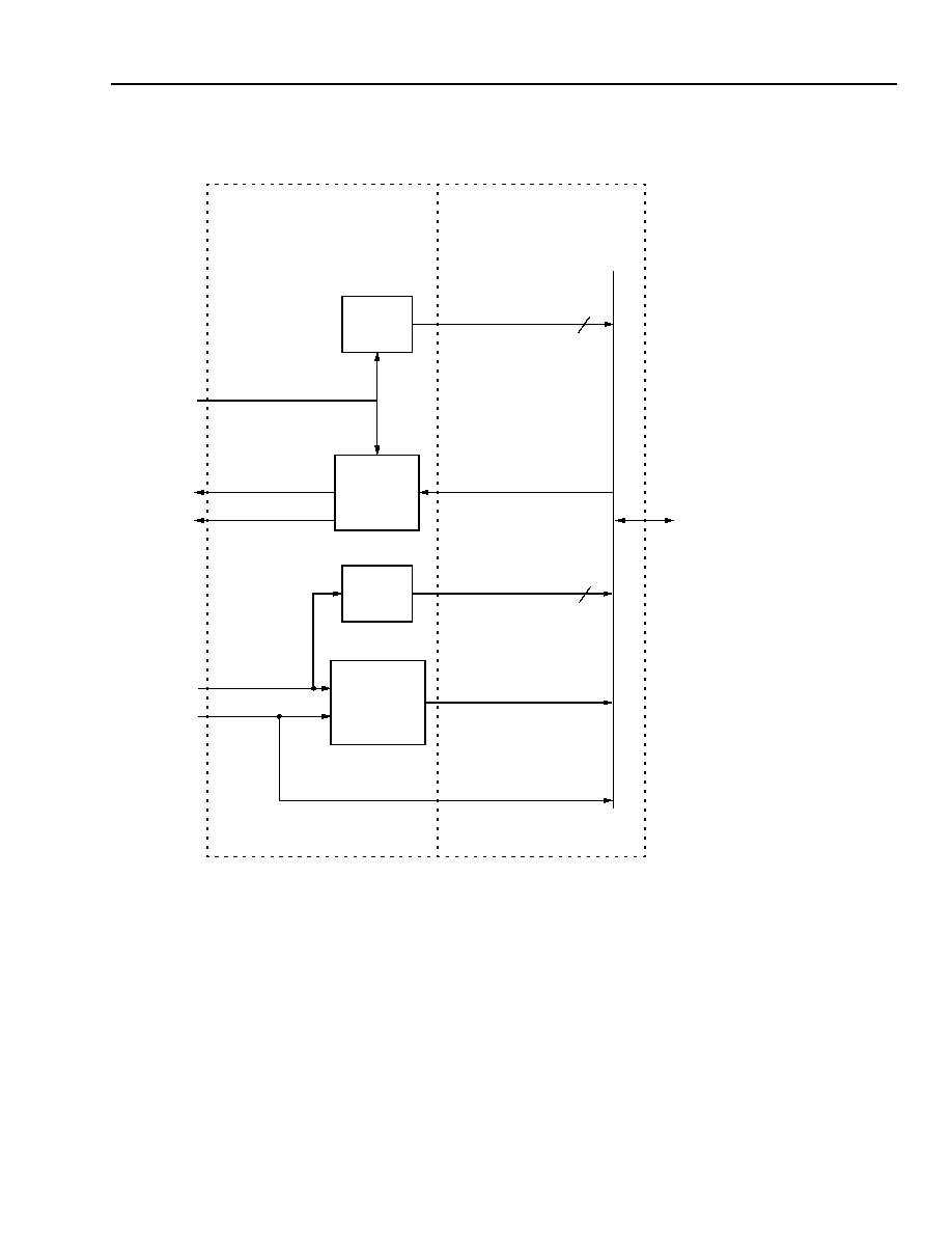
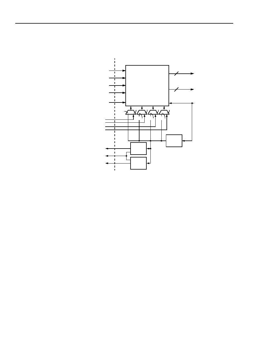
ORLI10G Overview
Device Layout
The ORLI10G FPSC provides a high-speed transmit
and receive line interface combined with FPGA logic.
The device is based on the 1.5 V OR4E4 FPGA. The
ORLI10G consists of an embedded backplane trans-
ceiver core and a full OR4E4 36x36 FPGA array.
The ORLI10G is a line interface device that contains an
FPGA base array, a 10 Gbits/s line interface block, and
programmable PLLs to do the overhead clock rate con-
versions on a single monolithic chip. The embedded
portion includes:
s
Line Interface: This consists of a 16-bit LVDS receive
data bus and a 16-bit LVDS transmit bus operating
up to 850 Mbits/s per input/output pair. Each 4-bit
LVDS
I/O has a high-speed LVDS clock (operating up to
850 MHz) associated with it.
s
MUX/deMUX: This performs the MUXing and
deMUXing between the high-speed line interface
data operating at the line rate and system data oper-
ating at 1/4 or 1/8 the line rate.
s
On-board PLLs: This is used to align system-side
data with the line-side data, which is at a slightly
higher data bandwidth than the system data because
of the addition of overhead due to encoding.
Figure 1 shows the ORLI10G block diagram.
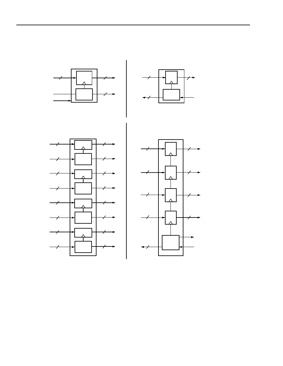
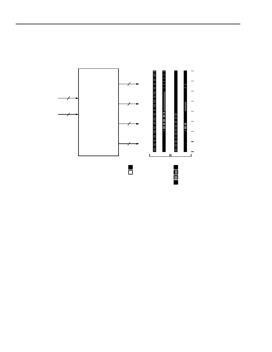
10G Mode
The ORLI10G can operate in one of two data modes:
10G mode or Quad 2.5G mode.
In 10G (or single-channel) mode, all 16 LVDS transmit
data outputs are assumed to be one data bus with one
LVDS clock provided off chip for the data. Likewise, all
16 LVDS receive data inputs are assumed to be one
data bus with one LVDS input clock provided for the
data.
Transmit Path
In 10G mode, the transmit data from the FPGA logic is
passed to the embedded core as a single 128- or 64-bit
bus. An off-chip transmit reference clock is divided
down in the core by 8 (for 128-bit to 16-bit MUX) or by
4 (for 64-bit to 16-bit MUX). All four transmit clock out-
puts are therefore synchronized.

12
12
Agere Systems Inc.
Data Sheet
October 2001
10 Gbits/s, and 12.5 Gbits/s Line Interface FPSC
ORCA ORLI10G Quad 2.5 Gbits/s
ORLI10G Overview
(continued)
Receive Path
The 16-bit receive data is deMUXed in the embedded
core to a single 128-bit or 64-bit data bus and passed
to the FPGA logic. The lowest-order LVDS input clock
(rx_clk_in[0]) is used as the receive clock for all 16 data
bits (the other three LVDS input clock pairs should be
tied low). This clock is divided down in the core by 8
(for 16-bit to 128-bit deMUX) or by 4 (for 16-bit to 64-bit
deMUX) and passed to the FPGA logic with the data.
The ORLI10G supports transmit and receive data rates
up to 850 Mbits/s. Therefore, the total data rate for this
mode is 850 Mbits/s x 16 or 13.6 Gbits/s.
2.5G Mode
In 2.5G (or quad-channel) mode, the 16 LVDS transmit
data outputs are assumed to be four 4-bit data buses
with four LVDS clocks provided off chip for each data
bus. Likewise, the 16 LVDS receive data inputs are
assumed to be four independent 4-bit data buses with
four LVDS asynchronous input clocks provided for
each data bus.
Transmit Path
In 2.5G mode, the transmit data from the FPGA logic is
passed to the embedded core as four separate 32- or
16-bit buses. A separate clock for each of the four bus-
ses is also passed to the core. An off-chip transmit ref-
erence clock is divided down in the core by 8 (for each
32 to 8-bit MUX) or by 4 (for each 16 to 4 MUX). This
divided down clock is used to resynchronize the output
data and clocks. All four transmit clock outputs are
therefore synchronized.
Receive Path
Each of the four 4-bit receive data buses are deMUXed
in the embedded core to one of four independent 32- or
16-bit data buses and passed to the FPGA logic. The
four receive clock inputs are divided down in the core
by 8 (for each 4- to 32-bit deMUX) or by 4 (for each
4- to 16-bit deMUX), and each divided clock is passed
to the FPGA logic with its associated data bus. All four
data paths act as separate data interfaces that are
asynchronous to each other.
The ORLI10G supports transmit and receive data rates
up to 850 Mbits/s. Therefore, the total data rate each of
the quad channels is 850 Mbits/s x 4 or 3.4 Gbits/s.
Figure 2 shows a representation of the 10G and 2.5G
modes in both transmit and receive directions.
Agere Systems Inc.
13
Data Sheet
October 2001
10 Gbits/s, and 12.5 Gbits/s Line Interface FPSC
ORCA ORLI10G Quad 2.5 Gbits/s
ORLI10G Overview
(continued)
1018(F)
Figure 1. ORCA ORLI10G Block Diagram
EMBEDDED CORE
FPGA LOGIC
(400K GATES)
TRANSMIT
PLLs
REFERENCE CLOCK
TRANSMIT DATA
16 x 622 OR
16 x 645 OR
16 x 667 OR
64:16 MUX
OR
128:16 MUX
TRANSMIT CLOCK
RECEIVE
PLLs
16:64 DEMUX
OR
16:128 DEMUX
RECEIVE DATA
16 x 622 OR
16 x 645 OR
16 x 667 OR
FOUR 2.5 Gbit RXCLKs
64-bit OR 128-bit
RXCLK
64-bit OR 128-bit
TXCLK
(167 MHz--78 MHz)
(167 MHz--78 MHz)
SYSTEM INTERFACE:
-- POS-PHY 4
-- XGMII
-- 156 MHz PECL
(OC-48/STM-16
SONET/SDH)
-- USER DEFINED
16 x 781 Mbits/s
16 x 781 Mbits/s
2
2
14
Agere Systems Inc.
Data Sheet
October 2001
10 Gbits/s, and 12.5 Gbits/s Line Interface FPSC
ORCA ORLI10G Quad 2.5 Gbits/s
ORLI10G Overview
(continued)
1335(F)
Figure 2. 10G (Single-Channel) and 2.5G (Quad-Channel) Modes
DATA
128 or 64
2.5G MODE
RECEIVE PATH
CORE
LVDS DATA
32 OR 16
FPGA
LVDS CLOCK
LVDS DATA
CORE
FPGA
CLOCK
32 OR 16
4
DEMUX
FPGA
CORE
LVDS DATA
16
RX_CLK_IN[0]
RX_CLK_IN[31:1]
CLOCK
1
DATA
4
DATA
MUX
TRANSMIT PATH
10G MODE
DIV BY 8
OR
DIV BY 4
DIV BY 8
DIV BY 8
MUX
LVDS
16
TX_CLK_IN
CORE
128 OR 64
FPGA
DATA
UNUSED
REFERENCE
DATA
TRANSMIT PATH
MUX
MUX
MUX
32 OR 16
DATA
32 OR 16
DATA
32 OR 16
DATA
LVDS DATA
4
LVDS DATA
4
LVDS DATA
4
DIV BY 8
OR
DIV BY 4
1
1
LVDS CLOCK
LVDS DATA
CLOCK
32 OR 16
4
DEMUX
DATA
DIV BY 8
OR
DIV BY 4
1
1
LVDS CLOCK
LVDS DATA
CLOCK
32 OR 16
4
DEMUX
DATA
DIV BY 8
OR
DIV BY 4
1
1
LVDS CLOCK
LVDS DATA
CLOCK
32 OR 16
4
DEMUX
DATA
DIV BY 8
OR
DIV BY 4
1
1
RECEIVE PATH
DEMUX
CLOCK
DIV BY 4
TX[1:2]VCOP
2
DIV BY 4
TX_CLK_IN
REFERENCE
CLOCK
TX_CLK_OUT[3:0]
LVDS CLOCKS
TX_CLK8_IN[3:0]
4

Agere Systems Inc.
15
Data Sheet
October 2001
10 Gbits/s, and 12.5 Gbits/s Line Interface FPSC
ORCA ORLI10G Quad 2.5 Gbits/s
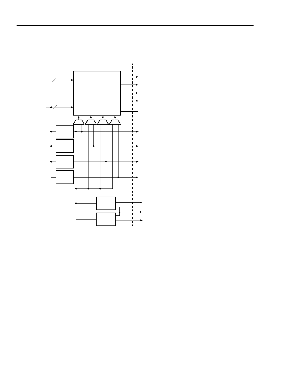
Receive Path Details
In the receive path, the ORLI10G embedded core can
be broken down into three sections: the high-speed line
interface, the demultiplexer, and the receive-side on-
board PLLs. Note that both transmit and receive PLLs
are in addition to the four programmable PLLs (PPLLs)
in the FPGA portion of the ORLI10G.
Line Interface
In the receive path, 16-bit data and associated clocks
are inputs to the line interface. Typical data rates are
expected to range from 622 Mbits/s to 850 Mbits/s for
most applications. The 16-bit LVDS input data bus is
actually composed of four 4-bit data buses with one
clock for each 4-bit data bus. In the 10G mode, all four
input clocks are tied together internal to the device and
driven by the lowest-order input clock. In 2.5G mode,
the four clocks may be asynchronous to each other.
The ORLI10G uses LVDS (low-voltage differential sig-
naling) drivers/receivers, which are intended to provide
point-to-point connection between the ORLI10G and
optical transceiver (MUX/deMUX) parts. The LVDS
inputs are hot-swap compatible and can connect to
other vendor's LVDS I/O buffers. The LVDS inputs are
terminated with a 100
resistor to improve perfor-
mance.
The receive line interface on the ORLI10G can connect
to devices that are compliant to either the XSBI stan-
dard or the SFI-4 standard. The major difference for
these standards is that for XSBI (IEEE 802.3ae version
2.1), the least significant bit [0] is received first after
deserialization by the external deMUX device, whereas
SFI-4 receives the most significant bit first. In some
cases, bits [15:0] on the ORLI10G should be con-
nected to bits [0:15] on the device to which the
ORLI10G device interfaces to. An example of this is
the PCS IP core in the ORLI10G when the ORLI10G is
connected to an XSBI version 2.1 device.
It should be noted that IEEE 802.3ae version 3.1
swaps XSBI so that the most significant bit is received
first, thus requiring that bits [0:15] on the ORLI10G be
connected directly to bits [0:15] on the XSBI device.
DeMUX
The demultiplexer takes the high-speed line data and
clocks and converts the data and clock to rates appro-
priate for transfer to the FPGA logic. The demultiplexer
supports two modes of operation:
s
Divide-by-8
10G (or single channel): The demultiplexer converts
the incoming 16 bits of data at 622 Mbits/s to
850 Mbits/s into 128 bits at 78 Mbits/s to 106 Mbits/s.
The incoming clocks are divided by 8.
2.5G (or quad channel): The demultiplexer converts
the incoming four bits of data at 622 Mbits/s to
850 Mbits/s into 32 bits at 78 Mbits/s to 106 Mbits/s.
The associated clock is also divided by 8. This is
repeated four times with each 4-bit data/clock group
assumed to be asynchronous to the others.
s
Divide-by-4
10G (or single channel): The demultiplexer converts
the incoming 16 bits of data at 622 Mbits/s to
850 Mbits/s into 64 bits at 156 Mbits/s to 212 Mbits/s.
The incoming clocks are divided by 4.
2.5G (or quad channel): The demultiplexer converts
the incoming 4 bits of data at 622 Mbits/s to
850 Mbits/s into 16 bits at 156 Mbits/s to 212 Mbits/s.
The associated clock is also divided by 4. This is
repeated four times with each 4-bit data/clock group
assumed to be asynchronous to the others.
Onboard Receive PLLs
The function of the onboard PLLs is to align the system
data with the line data which will be at a slightly higher
rate owing to the addition of the overhead bits. There
are two PLLs on the receive path. The input to the first
PLL, RX1_PLL (see Figure 3), is the divided down low-
est-order clock from the demultiplexer. The RX1_PLL
generates a clock with a user-defined frequency ratio
of M/N to the divided clock. This clock would generally
be used to compensate for different data rates due to
overhead bits. M and N can independently be set from
1 to 8.
The RX2_PLL also takes its input from the divided
down clock and is used to provide a balanced divided
clock across the FPGA-embedded core interface.
Both PLLs have delay loops which compensate for
routing delays to the embedded core/FPGA logic inter-
face for minimum clock skew.
In addition, the user can specify an additional skew on
each clock in increments of 1/8 the clock period.
The selection of the deMUX width (and corresponding
clock division value), the RX1_PLL M and N values,
and the additional skew for RX1_PLL and RX2_PLL
are specified by the user in a GUI interface provided in
the ORLI10G design kit.
A detailed block diagram of the receive path in shown
in Figure 3.
16
Agere Systems Inc.
Data Sheet
October 2001
10 Gbits/s, and 12.5 Gbits/s Line Interface FPSC
ORCA ORLI10G Quad 2.5 Gbits/s
Receive Path Details
(continued)
1333(F)
Figure 3. ORLI10G Embedded Core Receive Path Diagram
128 TO 16 MUX
OR
64 TO 16 MUX
DATA
RX_DAT_IN
16
CLOCK
RX_CLK_IN
4
FPGA LOGIC
DIVIDE BY 8 MODE
RX_DAT_OUT[127:96]
RX_DAT_OUT[95:64]
RX_DAT_OUT[63:32]
RX_DAT_OUT[31:0]
OR
RX_ENB_OUT[3:0]
DIVIDE BY 4 MODE
RX_DAT_OUT[111:96]
RX_DAT_OUT[79:64]
RX_DAT_OUT[47:32]
RX_DAT_OUT[15:0]
RX_CLK8_OUT[0]
RX_CLK8_OUT[1]
RX_CLK8_OUT[2]
RX_CLK8_OUT[3]
DIV BY 8
OR
DIV BY 4
ORLI10G CORE
RX1_PLL
(M/N)
RX2_PLL
(X1)
RX1_VCOP (X M/N CLOCK)
RX_LOCK
RX2_VCOP (X 1 CLOCK)
DIV BY 8
OR
DIV BY 4
DIV BY 8
OR
DIV BY 4
DIV BY 8
OR
DIV BY 4
RX_ENB_OUT[3:0]
RX1_VCO
RX2_VCO

Agere Systems Inc.
17
Data Sheet
October 2001
10 Gbits/s, and 12.5 Gbits/s Line Interface FPSC
ORCA ORLI10G Quad 2.5 Gbits/s
Transmit Path Details
In the transmit path, the ORLI10G embedded core can
be broken down into three sections: the multiplexer, the
transmit side onboard PLLs, and the high-speed line
interface. Note that both transmit and receive PLLs are
in addition to the four programmable PLLs (PPLLs) in
the FPGA portion of the ORLI10G.
MUX
The multiplexer takes data from the FPGA logic and
multiplexes the data to rates for transfer by the high-
speed line interface. The multiplexer supports two
modes of operation:
s
Multiplex-by-8
The multiplexer converts the incoming 128 bits of data
at 78 Mbits/s to 106 Mbits/s into 16 bits at 622 Mbits/s
to 850 Mbits/s. The incoming transmit reference clock
is divided by 8.
s
Multiplex-by-4
10G (or single channel): The multiplexer converts the
incoming 64 bits of data at 156 Mbits/s to 212 Mbits/s
into 16 bits at 622 Mbits to 850 Mbits/s. The transmit
reference clock is divided by 4.
Onboard Transmit PLLs
The function of the onboard PLLs is to align the system
data with the line data which will be at a slightly higher
rate owing to the addition of the overhead bits. There
are two PLLs on the transmit path. The input to the first
PLL, TX1_PLL (see Figure 4), is the divided down
transmit reference clock from the multiplexer. The
TX1_PLL generates a clock with a user-defined fre-
quency ratio of M/N to the divided clock. This clock
would generally be used to compensate for different
data rates due to overhead bits. M and N can be inde-
pendently set from 1 to 8.
The TX2_PLL also takes its input reference from the
divided down reference clock and is used to provide a
balanced divided clock across the FPGA-embedded
core interface.
Both PLLs have delay loops which compensate for
routing delays to the embedded core/FPGA logic inter-
face for minimum clock skew.
In addition, the user can specify an additional skew on
each clock in increments of 1/8 the clock period.
The selection of the MUX width (and corresponding
clock division value), the TX1_PLL M and N values,
and the additional skew for TX1_PLL and TX2_PLL are
specified by the user in a GUI interface provided in the
ORLI10G design kit.
A detailed block diagram of the transmit path in shown
in Figure 4. In 10 Gbit mode, either TX1_VCOP or
TX2_VCOP must be used to clock TX_DAT_IN[127:0]
that is transmitted to the embedded block. These PLLs
can also be bypassed, where the divided transmit ref-
erence clock is sent directly to the FPGA. In 2.5 Gbit
mode, TX_CLK8_IN[3:0] is used to clock data transmit-
ted to the embedded block.
Line Interface
In the transmit path, 16-bit data and associated clocks
are outputs from the line interface. Typical data rates
are expected to range from 622 Mbits/s to 850 Mbits/s
for most applications. The 16-bit LVDS output data bus
is actually composed of four 4-bit data buses with one
clock for each 4-bit data bus. On the transmit side,
these clocks will all be synchronized. The ORLI10G
uses LVDS (low-voltage differential signaling)
drivers/receivers, which are intended to provide point-
to-point connection between the ORLI10G and optical
transceiver (MUX/deMUX) parts. The LVDS drivers are
hot-swap compatible and can connect to other
vendor's LVDS I/O buffers. The LVDS drivers are
terminated with a 100
resistor to improve
performance.
The transmit line interface on the ORLI10G can con-
nect to devices that are compliant to either the XSBI
standard or the SFI-4 standard. The major difference
for these standards is that for XSBI, the least signifi-
cant bit [0] is transferred first after serialization by the
external MUX device, whereas SFI-4 transmits the
most significant bit first. In some cases, bits [15:0] on
the ORLI10G should be connect to bits [0:15] on the
device to which the ORLI10G device interfaces to. An
example of this is the PCS IP core in the ORLI10G
when the ORLI10G is connected to an XSBI version
2.1 device.
It should be noted that IEEE 802.3ae version 3.1
swaps XSBI so that the most significant bit is trans-
ferred first, thus requiring that bits [0:15] on the
ORLI10G be connected directly to bits [0:15] on the
XSBI device.
18
Agere Systems Inc.
Data Sheet
October 2001
10 Gbits/s, and 12.5 Gbits/s Line Interface FPSC
ORCA ORLI10G Quad 2.5 Gbits/s
Transmit Path Details
(continued)
1332(F)
Figure 4. ORLI10G Embedded Core Transmit Path Diagram
128 TO 16 MUX
OR
64 TO 16 MUX
DATA
TX_DAT_OUT
16
CLOCK
TX_CLK8_OUT
4
TRANSMIT REFERENCE
CLOCK
FPGA LOGIC
DIVIDE BY 8 MODE
TX_DAT_IN[127:96]
TX_DAT_IN[95:64]
TX_DAT_IN[63:32]
TX_DAT_IN[31:0]
OR
TX_ENB_IN[3:0]
DIVIDE BY 4 MODE
TX_DAT_IN[111:96]
TX_DAT_IN[79:64]
TX_DAT_IN[47:32]
TX_DAT_IN[15:0]
10G
2.5G
TX_CLK8_IN[0]
TX_CLK8_IN[1]
TX_CLK8_IN[2]
TX_CLK8_IN[3]
DIV BY 8
OR
DIV BY 4
TX_CLK_IN
ORLI10G CORE
TX1_PLL
(M/N)
TX2_PLL
(X1)
TX1_VCOP (X M/N CLOCK)
TX_LOCK
TX2_VCOP (X 1 CLOCK)
2.5G
2.5G
2.5G
10G
10G
10G
TX_ENB_IN[3:0]
TX1_VCO
TX2_VCO

Agere Systems Inc.
19
Data Sheet
October 2001
10 Gbits/s, and 12.5 Gbits/s Line Interface FPSC
ORCA ORLI10G Quad 2.5 Gbits/s
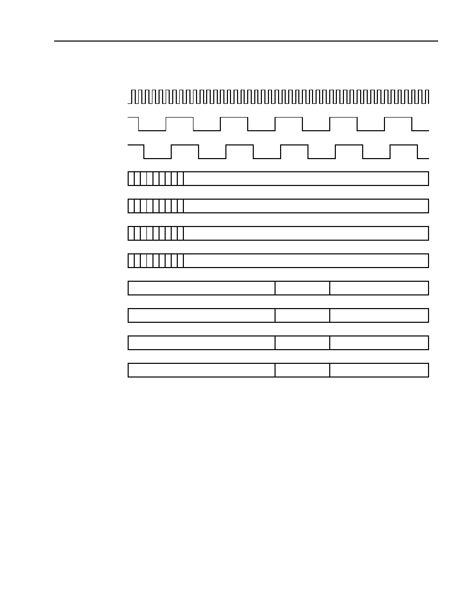
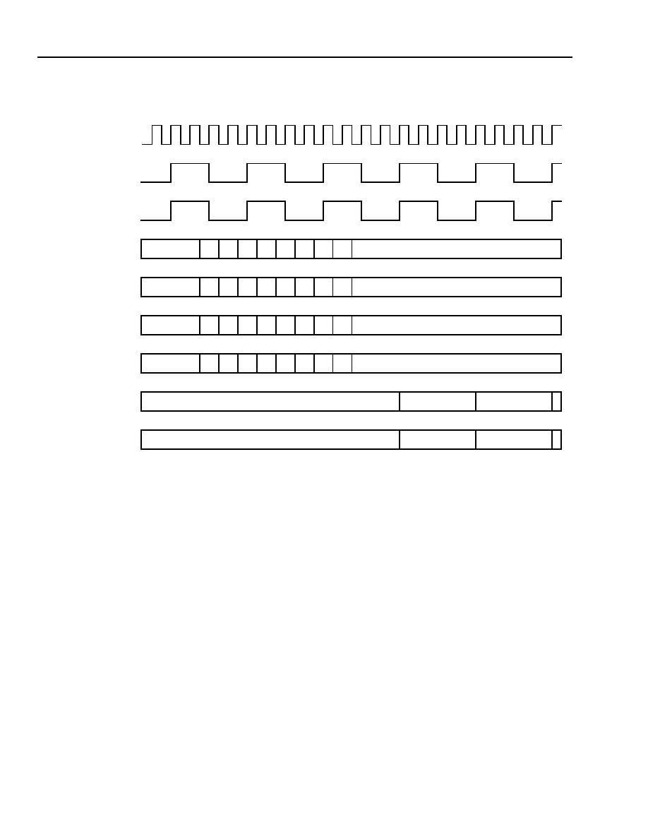
ORLI10G Demultiplexer (Rx) Detail
The demultiplexer module converts the incoming
16 bits of data at 622 MHz/850 MHz into 128 bits of
data at 78 MHz/106 MHz or 64 bits of data at
156 MHz/212 MHz and sends it to the FPGA logic. It
has been implemented in two stages: the first stage
converts each incoming bit into a byte stream and the
second stage bit interleaves these bytes into
128/64 bits, depending upon the mode of operation.
The low-speed clocks are generated by this block.
These clocks are then driven back to this block from
the low-speed clock tree network. Functionally, the
demultiplexer architecture consists of three blocks: the
serial to parallel conversion, the counters, and the
interleaving.
The first stage of the line interface module (demulti-
plexer) converts each incoming bit of data into a byte
stream on a divided-by-8 clock. The data is first regis-
tered on the rising edge of the clock input. The clock
dividers also runs parallel to data shift (serial to paral-
lel), on the rising edge of the input clock. An enable is
created when a complete byte is taken in. This enable
signal is used to register the serial-to-parallel con-
verted data at the high-speed input clock. This ensures
that the data can be safely transferred to the low-speed
clock. This data is then transferred to the divided clock,
allowing a timing margin of approximately half the
divided clock period.
The high-speed demultiplexer converts the incoming
data as blocks of bytes. The byte boundaries of incom-
ing data are unknown and are irrelevant to this module.
This data is then interleaved to the 128/64 bits of out-
put data, depending on the mode of operation (divide-
by-4/divide-by-8). In 10G mode, the output data is
assigned the retimed 128/64 bits of data from the first
stage of line interface registered at the input clock [0].
In 2.5G mode, the output data is assigned four concat-
enated 32/16 bits of data from the first stage of line
interface registered at input clocks [0 to 3]. The inter-
leaving is done at bit level because the serial-to-paral-
lel converter operates on bits of incoming data. In 10G
mode, it is assumed that all the incoming 16 bits of
data are synchronized to the input clock [0]. This block
also generates the clock enables used by the output
line interface (multiplexer) module for registering the
data on the high-speed clock. These enables along
with the enables from other clocks are selected through
the high-speed clock MUX for the output line interface
block.
20
Agere Systems Inc.
Data Sheet
October 2001
10 Gbits/s, and 12.5 Gbits/s Line Interface FPSC
ORCA ORLI10G Quad 2.5 Gbits/s
ORLI10G Demultiplexer (Rx) Detail
(continued)
Figure 5 shows the valid data output bits from the demultiplexer in each of the four modes (divide-by-8, 10G and
2.5G modes, and divide-by-4, 10G and 2.5G modes). Figure 6--Figure 9 show the demultiplexer input data and
clock waveforms and output clock, enable, and data waveforms for all four modes.
1338(F)
Figure 5. Demultiplexer Output Data Structure
4x4 TO 32 DEMUX
OR
4x4 TO 16 DEMUX
RX_DAT_OUT
16 OR 32
RX_DAT_OUT
16 OR 32
RX_DAT_OUT
16 OR 32
RX_DAT_OUT
16 OR 32
RX_DAT_IN
16
RX_CLK_IN
4
128
112
96
80
64
48
32
16
0
10G 2.5G
˜
8 MODE
˜
4 MODE
2.5G
10G
UNDEFINED
SINGLE CHANNEL
CHANNEL 3
CHANNEL 2
CHANNEL 1
CHANNEL 0
Agere Systems Inc.
21
Data Sheet
October 2001
10 Gbits/s, and 12.5 Gbits/s Line Interface FPSC
ORCA ORLI10G Quad 2.5 Gbits/s
ORLI10G Demultiplexer (Rx) Detail
(continued)
1340(F)
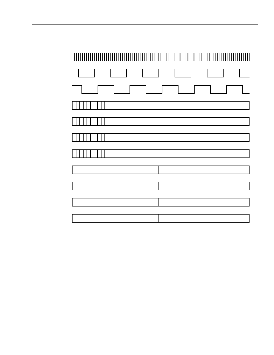
Figure 6. Demultiplexer Serial-to-Parallel Conversion--Divide by 8, 10G Mode
(RX_ENB8_OUT[1:3] = 0)
0 0 4 8 C 1 9 0 8
0
0 1 5 9 D 3 B 2 A
0
0 2 6 A E 5 D 4 C
0
0 3 7 B F 7 F 6 E
0
00000000
01234567
0
00000000
89ABCDEF
0
00000000
13579BDF
0
00000000
02468ACE
0
RX_CLK_IN0
RX_CLK8_OUT0
(RX_CLK8_OUT[1:3] = 0)
RX_DAT_IN
[15:12]
RX_ENB8_OUT0
RX_DAT_IN
[11:8]
RX_DAT_IN
[7:4]
RX_DAT_IN
[3:0]
RX_DAT_OUT
[127:96]
RX_DAT_OUT
[95:64]
RX_DAT_OUT
[63:32]
RX_DAT_OUT
[31:0]
22
Agere Systems Inc.
Data Sheet
October 2001
10 Gbits/s, and 12.5 Gbits/s Line Interface FPSC
ORCA ORLI10G Quad 2.5 Gbits/s
ORLI10G Demultiplexer (Rx) Detail
(continued)
1341(F)
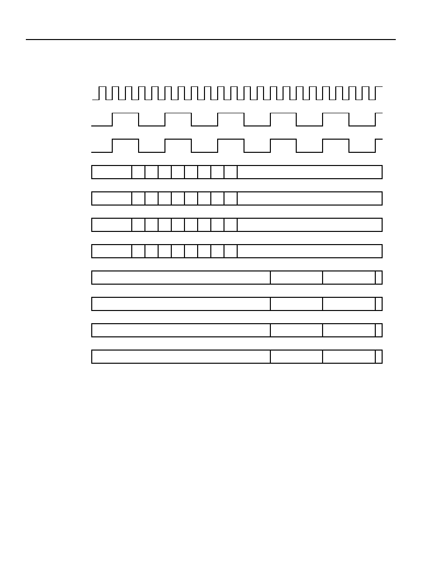
Figure 7. Demultiplexer Serial-to-Parallel Conversion--Divide by 4, 10G Mode
0
0
4
8
C
1
9
0
8
0
00000000
01234567
0
(RX_ENB8_OUT[1:3] = 0)
RX_CLK_IN0
RX_CLK8_OUT0
(RX_CLK8_OUT[1:3] = 0)
RX_DAT_IN
[15:12]
RX_ENB8_OUT0
RX_DAT_IN
[11:8]
RX_DAT_IN
[7:4]
RX_DAT_IN
[3:0]
RX_DAT_OUT
[63:32]
RX_DAT_OUT
[31:0]
0
1
5
9
D
3
B
2
A
0
0
2
6
A
E
5
D
4
C
0
0
3
7
B
F
7
F
6
E
0
13579BDF
00000000
89ABCDEF
0
02468ACE
Agere Systems Inc.
23
Data Sheet
October 2001
10 Gbits/s, and 12.5 Gbits/s Line Interface FPSC
ORCA ORLI10G Quad 2.5 Gbits/s
ORLI10G Demultiplexer (Rx) Detail
(continued)
1342(F)
Figure 8. Demultiplexer Serial-to-Parallel Conversion--Divide by 8, 2.5G Mode
0 0 1 2 3 4 5 6 7
0
0 8 9 A B C D E F
0
0 1 3 5 7 9 B D F
0
0 0 2 4 6 8 A C E 0
00000000
01234567
0
00000000
89ABCDEF
0
00000000
13579BDF
0
00000000
02468ACE
0
RX_CLK_IN[0:3]
RX_CLK8_OUT[0:3]
RX_DAT_IN
[15:12]
RX_ENB8_OUT[3:0]
RX_DAT_IN
[11:8]
RX_DAT_IN
[7:4]
RX_DAT_IN
[3:0]
RX_DAT_OUT
[127:96]
RX_DAT_OUT
[95:64]
RX_DAT_OUT
[63:32]
RX_DAT_OUT
[31:0]
24
Agere Systems Inc.
Data Sheet
October 2001
10 Gbits/s, and 12.5 Gbits/s Line Interface FPSC
ORCA ORLI10G Quad 2.5 Gbits/s
ORLI10G Demultiplexer (Rx) Detail
(continued)
1343(F)
Figure 9. Demultiplexer Serial-to-Parallel Conversion--Divide by 4, 2.5G Mode
0
0
1
2
3
4
5
6
7
0
0000
0123
0
RX_CLK_IN[3:0]
RX_CLK8_OUT[3:0]
RX_DAT_IN
[15:12]
RX_ENB8_OUT[3:0]
RX_DAT_IN
[11:8]
RX_DAT_IN
[7:4]
RX_DAT_IN
[3:0]
RX_DAT_OUT
[111:96]
RX_DAT_OUT
[79:64]
0
8
9
A
B
C
D
E
F
0
0
1
3
5
7
9
B
D
F
0
0
0
2
4
6
8
A
C
E
0
4567
0000
89AB
0
CDEF
0000
1357
0
9BDF
0000
0246
0
8ACE
RX_DAT_OUT
[47:32]
RX_DAT_OUT
[15:0]

Agere Systems Inc.
25
Data Sheet
October 2001
10 Gbits/s, and 12.5 Gbits/s Line Interface FPSC
ORCA ORLI10G Quad 2.5 Gbits/s
ORLI10G Multiplexer (Tx) Detail
The multiplexer module converts the incoming 128 bits
of data from the FPGA logic at 78 MHz/106 MHz or
64 bits of data from the FPGA logic at 156 MHz/212
MHz into 16 bits of data at 622 MHz/850 MHz. It has
been implemented as two stages. The first stage
deinterleaves each incoming byte into a different byte
stream that can be serially output on the output data
pins. The second stage outputs these bytes into 16 bits
or four groups of 4 bits, depending upon the mode of
operation. Functionally, the multiplexer architecture
consists of three blocks: the parallel-to-serial
conversion, the counters, and the deinterleaving.
For 2.5G divide-by-8 mode, the first stage of the line
interface module deinterleaves each incoming byte of
data into a different byte stream on the
78 MHz/106 MHz (TX_CLK8_IN[3:0]) clock. This data
is then registered on the rising edge of the
622 MHz/850 MHz (TX_CLK_IN) clock at the falling
edge of the 78 MHz/106 MHz clock. The enable inputs
(TX_ENB8_IN[3:0]) are used to transfer data from the
low-speed clock to the high-speed clock, as well as
synchronizing the counters of parallel-to-serial
conversion which are running at the high-speed clock.
For 2.5G divide-by-4 mode, the first stage of the line
interface module deinterleaves each incoming byte of
data into a different byte stream on the
156 MHz/212 MHz (TX_CLK8_IN[3:0]) clock. This data
is then registered on the rising edge of the
622 MHz/850 MHz (TX_CLK_IN) clock at the falling
edge of the 156 MHz/212 MHz clock. The enable
inputs (TX_ENB8_IN[3:0]) are used to transfer data
from the low-speed clock to the high-speed clock, as
well as synchronizing the counters of parallel-to-serial
conversion which are running at the high-speed clock.
In 2.5G modes, the enable inputs (TX_ENB8_IN[3:0])
are required to be four (divide by 4) or eight (divide by
8) TX_CLK_IN clock cycles wide. They have to be
synchronous to their corresponding TX_CLK8_IN[3:0]
clock. Each of these four TX_CLK8_IN[3:0] clocks
must also be frequency locked to the TX_CLK_IN
signal.
In 10G modes, the enable inputs (TX_ENB8_IN[3:0])
are also required to be four (divide by 4) or eight (divide
by 8) TX_CLK_IN clock cycles wide. In 10G modes,
the other enable inputs (TX_ENB8_IN[3:1]) are
unused. Unlike 2.5G modes, this enable is
synchronous to a divided version of TX_CLK_IN from
the embedded core. In 10G modes, the
TX_CLK8_IN[3:0] inputs are not used. For version 2
ORLI10G devices, the enable signal can also
optionally be generated automatically in the embedded
core, thus removing the need to supply TX_ENB8_IN0
when that mode is selected. A second new option for
the version 2 ORLI10G devices will synchronize the
TX_ENB8_IN0 enable with the divided version of
TX_CLK_IN in the embedded core to simplify timing.
In both 2.5G and 10G modes, the TX_CLK_OUT[3:0]
clock outputs from the ORLI10G are provided for
transferring each 4 bits of data per clock.
For both 2.5G modes and 10G modes, all data to be
transmitted to the embedded core must be frequency
locked to the TX_CLK_IN signal. Thus, the divided
version of this clock found at the embedded core
interface should always be used to transfer data from
the FPGA logic to the embedded core. In 2.5G modes,
this same clock signal should also be used to generate
the enable signals as discussed previously. These
clock signals are available from the TX PLL outputs
(TX1_VCO, TX1_VCOP, TX2_VCO, TX2_VCOP).
Figure 10 shows the valid data input bits to the
multiplexer in each of the four modes (divide-by-8, 10G
and 2.5G modes, and divide-by-4, 10G and 2.5G
modes). Figure 11--Figure 14 show the multiplexer
input transmit reference clock, data, enable, and clock
waveforms and output clock and data waveforms for all
four modes.
In version 2 of the ORLI10G device, additional
capabilities are added to the Multiplexer block. The first
allows the clock inputs TX_CLK8_IN[3:0] to be
optionally generated in the embedded core in 2.5G
mode, as is done for 10G mode for version 1. The
second option allows all enables TX_ENB8_IN[3:0] to
be generated in the embedded core for both 2.5G and
10 G modes. The third option allows the enable inputs
TX_ENB8_IN[3:0] to continue to be used, but they are
re-synchronized in the embedded core before being
used. All options allow for simplification of the FPGA to
embedded core interface. If none are selected, the
ORLI10G defaults to version 1 compatible operation.
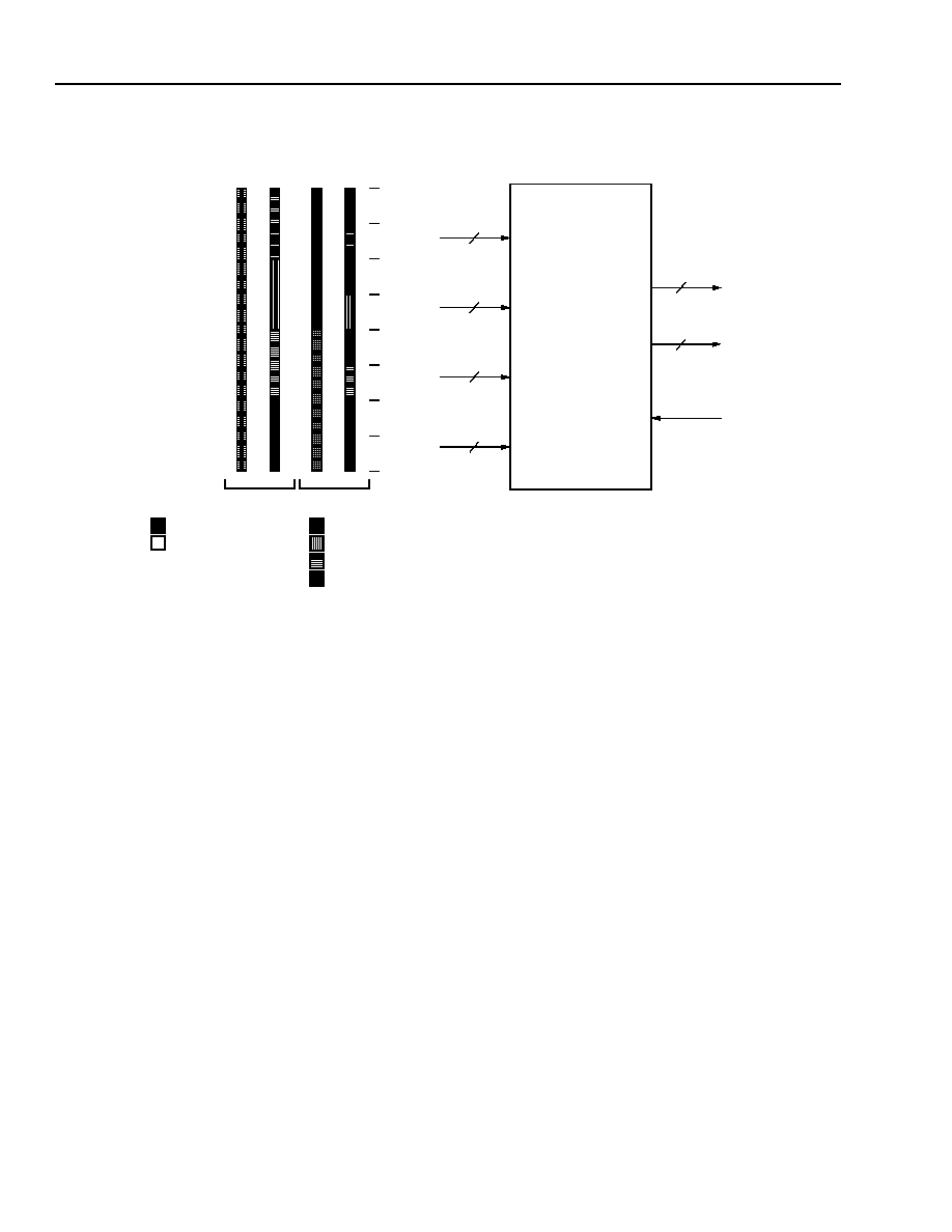
26
Agere Systems Inc.
Data Sheet
October 2001
10 Gbits/s, and 12.5 Gbits/s Line Interface FPSC
ORCA ORLI10G Quad 2.5 Gbits/s
ORLI10G Multiplexer (Tx) Detail
(continued)
1339(F)
Figure 10. Multiplexer Input Data Structure
4x4 TO 32 DEMUX
OR
4x4 TO 16 DEMUX
TX_DAT_IN
16 OR 32
TX_DAT_IN
16 OR 32
TX_DAT_IN
16 OR 32
TX_DAT_IN
16 OR 32
TX_DAT_OUT
16
TX_CLK_OUT
4
TRANSMIT
REFERENCE
CLOCK
TX_CLK_IN
128
112
96
80
64
48
32
16
0
10G 2.5G
˜
8 MODE
˜
4 MODE
2.5G
10G
UNDEFINED
SINGLE CHANNEL
CHANNEL 3
CHANNEL 2
CHANNEL 1
CHANNEL 0
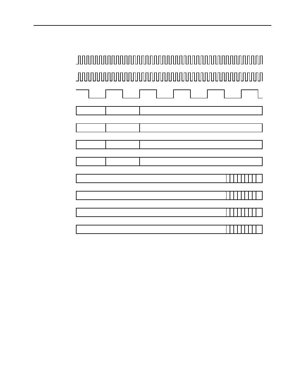
Agere Systems Inc.
27
Data Sheet
October 2001
10 Gbits/s, and 12.5 Gbits/s Line Interface FPSC
ORCA ORLI10G Quad 2.5 Gbits/s
ORLI10G Multiplexer (Tx) Detail
(continued)
1344(F)
Figure 11. Multiplexer Parallel-to-Serial Conversion--Divide by 8, 10G Mode
00000000
TX_CLK_IN
TX_CLK8_OUT[3:0]
TX_DAT_OUT
[15:12]
TX_DAT_OUT
[11:8]
TX_DAT_OUT
[7:4]
TX_DAT_OUT
[3:0]
TX_DAT_IN
[127:96]
TX_DAT_IN
[95:64]
TX_DAT_IN
[63:32]
TX_DAT_IN
[31:0]
TX_ENB8_IN0
01234567
0
00000000
89ABCDEF
0
00000000
13579BDF
0
00000000
02468ACE
0
0 4 8 C 1 9 0 8
0
0
1 5 9 D 3 B 2 A 0
0
2 6 A E 5 D 4 C 0
0
3 7 B F 7 F 6 E 0
0
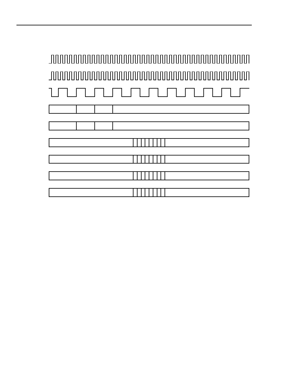
28
Agere Systems Inc.
Data Sheet
October 2001
10 Gbits/s, and 12.5 Gbits/s Line Interface FPSC
ORCA ORLI10G Quad 2.5 Gbits/s
ORLI10G Multiplexer (Tx) Detail
(continued)
1345(F)
Figure 12. Multiplexer Parallel-to-Serial Conversion--Divide by 4, 10G Mode
TX_CLK_IN
TX_CLK_OUT[3:0]
TX_DAT_IN
[63:32]
TX_DAT_IN
[31:0]
TX_ENB8_IN0
13579BDF
0 4 8 C 1 9 0 8 0
0
1 5 9 D 3 B 2 A 0
0
2 6 A E 5 D 4 C 0
0
3 7 B F 7 F 6 E 0
0
00000000
01234567
0
02468ACE
00000000
89ABCDEF
0
TX_DAT_OUT
[15:12]
TX_DAT_OUT
[11:8]
TX_DAT_OUT
[3:0]
TX_DAT_OUT
[7:4]
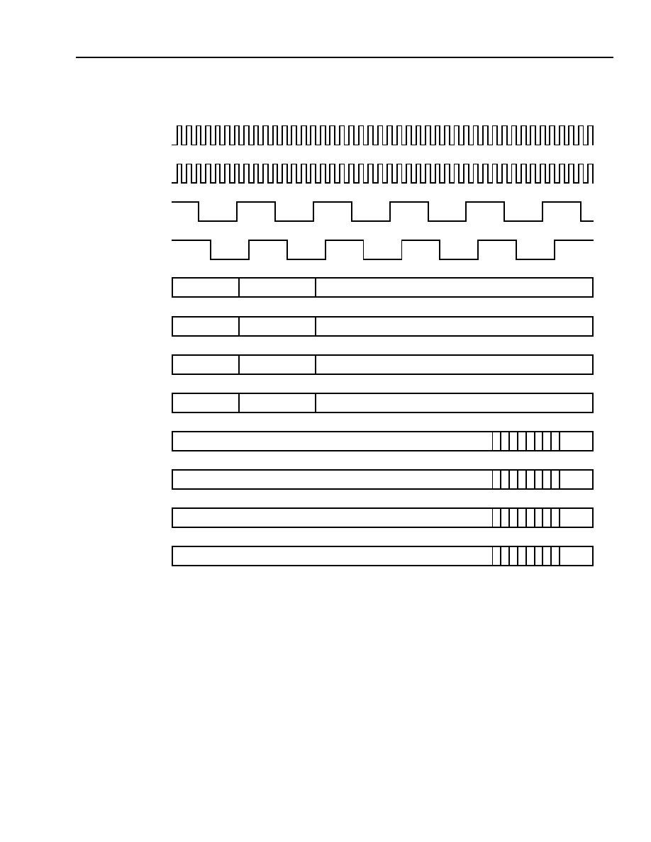
Agere Systems Inc.
29
Data Sheet
October 2001
10 Gbits/s, and 12.5 Gbits/s Line Interface FPSC
ORCA ORLI10G Quad 2.5 Gbits/s
ORLI10G Multiplexer (Tx) Detail
(continued)
1346(F)
Figure 13. Multiplexer Parallel-to-Serial Conversion--Divide by 8, 2.5G Mode
00000000
TX_CLK_IN
TX_CLK8_OUT[3:0]
TX_DAT_OUT
[15:12]
TX_DAT_OUT
[11:8]
TX_DAT_OUT
[7:4]
TX_DAT_OUT
[3:0]
TX_DAT_IN
[127:96]
TX_DAT_IN
[95:64]
TX_DAT_IN
[63:32]
TX_DAT_IN
[31:0]
TX_CLK8_IN[3:0]
TX_ENB8_IN[3:0]
01234567
0
00000000
89ABCDEF
0
00000000
13579BDF
0
00000000
02468ACE
0
0 1 2 3 4 5 6 7
0
0
8 9 A B C D E F
0
0
1 3 5 7 9 B D F
0
0
0 2 4 6 8 A C E
0
0
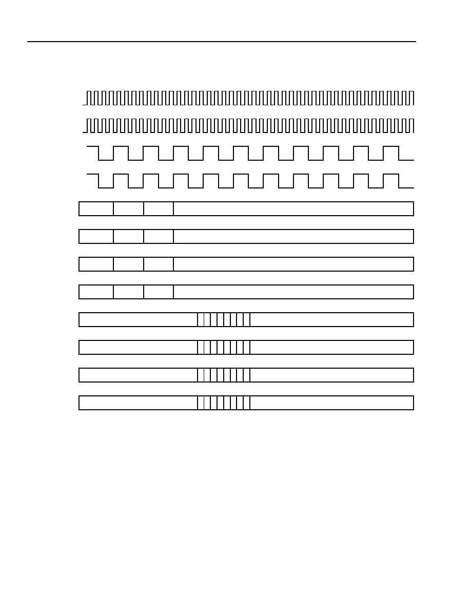
30
Agere Systems Inc.
Data Sheet
October 2001
10 Gbits/s, and 12.5 Gbits/s Line Interface FPSC
ORCA ORLI10G Quad 2.5 Gbits/s
ORLI10G Multiplexer (Tx) Detail
(continued)
1347(F)
Figure 14. Multiplexer Parallel-to-Serial Conversion--Divide by 4, 2.5G Mode
TX_CLK_IN
TX_CLK_OUT[3:0]
TX_DAT_IN
[111:96]
TX_DAT_IN
[79:64]
TX_CLK8_IN[3:0]
TX_ENB8_IN[3:0]
4567
0 1 2 3 4 5 6 7 0
0
8 9 A B C D E F 0
0
1 3 5 7 9 B D F 0
0
0 2 4 6 8 A C E 0
0
0000
0123
0
TX_DAT_IN
[47:32]
TX_DAT_IN
[15:0]
TX_DAT_OUT
[31:0]
TX_DAT_OUT
[63:32]
CDEF
0000
89AB
0
9BDF
0000
1357
0
8ACE
0000
0246
0
TX_DAT_OUT
[63:32]
TX_DAT_OUT
[31:0]
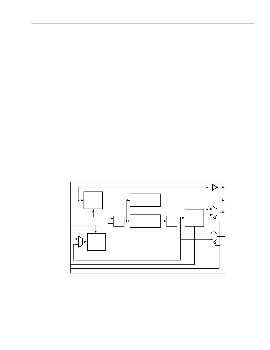
Agere Systems Inc.
31
Data Sheet
October 2001
10 Gbits/s, and 12.5 Gbits/s Line Interface FPSC
ORCA ORLI10G Quad 2.5 Gbits/s
ORLI10G Embedded PLLs
The ORLI10G embedded (transmit and receive) PLLs are based on the 4E series FPGA high-speed programma-
ble PLL (HPPLL). The 4E PLL consists of a phase/frequency detector (PFD), a charge pump/filter, a multitap volt-
age controlled oscillator (VCO), a duty cycle synthesis circuitry, a power regulator, two programmable dividers,
phase shift selector multiplexers, a lock signal generator, and a current DAC. A block diagram of the programma-
ble PLL is shown in Figure 15. The receive path RX1_PLL and transmit path TX1_PLL, which can be programmed
to create a N/M frequency clock, are based on this design.
The receive path RX2_PLL and transmit path TX2_PLL create a X1 clock. This is essentially the same PLL without
the M and N divider.
The RCKI input to the PLLs comes from an input clock to the ORLI10G that has been divided in frequency by
either 4 or 8 (programmable). As shown in Figure 3, RX1_PLL and RX2_PLL are driven by the divided version of
RX_CLK_IN0. As shown in Figure 4, TX1_PLL and TX2_PLL are driven by the divided versions of TX_CLK_IN. It
should be noted that the speed of the ORLI10G line interface is therefore either 4X or 8X the operating speed of
the embedded PLLs.
The clock feedback loops for the RX2_PLL and TX2_PLL should be routed from the clock network in the FPGA
core so as to compensate for the routing delays to the FPGA logic interface. The source to the TX2_FBCKI or
RX2_FBCKI inputs must come from an FPGA clock network driven by the VCO output (otherwise any phase shift-
ing on VCOP is removed by the feedback loops). In this way, the clock skew at the embedded core/FPGA logic
boundary is zero for the receive and transmit PLLs.
All PLLs include a phase shift selector which allows phase shift adjustments of each clock in increments of 1/8 the
period of the clock. This phase shifted output is available on the VCOP output of the PLL.
All functions of the embedded core PLLs are user controlled through a GUI provided with the ORLI10G Design Kit
software.
1331(F)
Figure 15. ORLI10G Programmable PLL Block Diagram
RCKI
M<5:0>
N<5:0>
SEL<2:0>
BYPASS
M
DIVIDER
N
DIVIDER
PFD
LOCK
GENERATOR
CHARGE PUMP
AND FILTER
VCO
PHASE
SELECT
RCKO
LOCK
VCOP
VCO
TX2_FBCKI
RX2_FBCKI
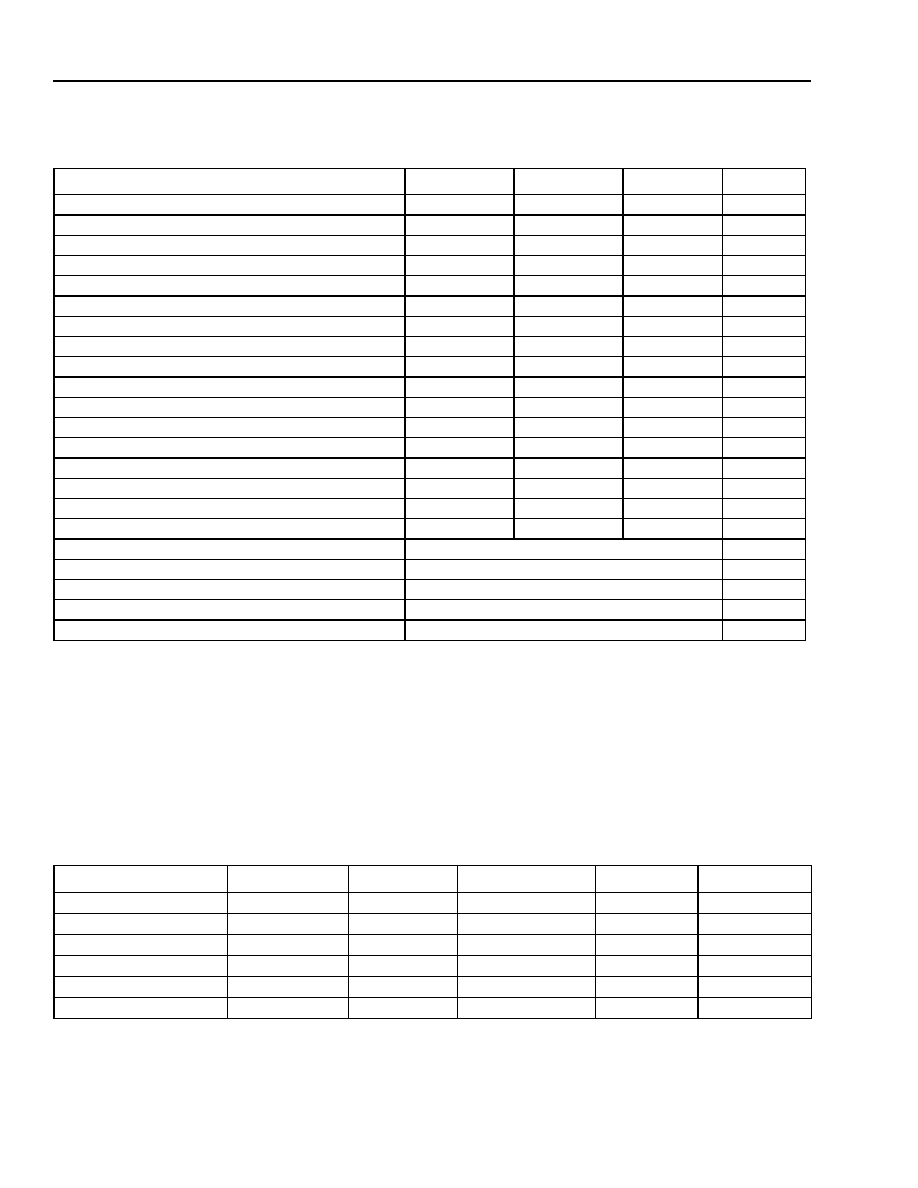
32
Agere Systems Inc.
Data Sheet
October 2001
10 Gbits/s, and 12.5 Gbits/s Line Interface FPSC
ORCA ORLI10G Quad 2.5 Gbits/s
ORLI10G Embedded Programmable PLLs Specifications
Table 2. Programmable PLL Specifications
Notes:
Multiplication and division values can both be used on one PLL output (example 3/4x).
For more information, see the Series 4 PLL Application Note.
ORLI10G Reset Requirements
Both the embedded core portion and the FPGA portion are reset at powerup. The embedded core is also reset, as
shown in Table 3, based on other conditions. For version 1 ORLI10G devices, these resets are all asynchronous
and must be held in reset for at least 8 ns. For version 2, the resets can also optionally be set to be asynchronous
on with synchronous release. Table 3 also shows the conditions upon which the I/O are 3-stated.
Table 3. ORLI10G Reset Requirements
Typically, the following reset sequence should be followed for the ORLI10G:
s
Place the device in reset by driving RESET_TX = 1, RESET_RX = 1, and by placing the FPGA portion into reset.
s
Release the embedded core from reset by driving RESET_TX = 0 and RESET_RX = 0.
s
Release the FPGA portion from reset.
Parameters
Min
Nom
Max
Unit
V
DD
15
1.425
1.5
1.575
V
V
DD
33
3.0
3.3
3.6
V
Operating Temperature
≠40
--
125
∞C
Input Clock Frequency
60
--
420
MHz
Input Duty Cycle
30
--
70
%
Input Clock Jitter Requirement
--
--
TBD
UIp-p
Input Jitter Transfer
--
--
TBD
UIp-p
Output Clock Frequency
60
--
420
MHz
Output Duty Cycle
45
50
55
%
dc Power Consumption
--
50
--
mW
Total On Current (dc)
--
14
--
mA
Total Off Current (dc)
--
30.0
--
pA
Cycle to Cycle Jitter (p-p)
--
<0.02
TBD
UIp-p
Period Jitter (p-p)
TBD
TBD
TBD
UIp-p
Duty Cycle Jitter (p-p)
TBD
TBD
TBD
UIp-p
VCO Output vs. VCOP Output Jitter
--
--
TBD
ps
Lock Time
--
<50
--
µS
Frequency Multiplication (TX1_PLL and RX1_PLL)
2x, 3x, 4x, 5x, 6x, 7x, 8x
--
Frequency Division (TX1_PLL and RX1_PLL)
1/8x, 1/7x, 1/6x, 1/5x, 1/4x, 1/3x, 1/2x
--
Duty Cycle Adjust of Output Clock(s)
12.5, 25, 37.5, 50, 62.5, 75, 87.5
%
Delay Adjust of Output Clock
0, 45, 90, 135, 180, 225, 270, 315
degrees
Phase Shift Between VCO and VCOP
0, 45, 90, 135, 180, 225, 270, 315
degrees
Condition
TX MUX Block
TX PLL
RX DeMUX Block
RX PLL
Embedded I/O
Powerup
Reset
Reset
Reset
Reset
3-state
FPGA Configuration
Reset
Reset
Reset
Reset
Active
TS_ALL Pin = 1
--
--
--
--
3-state
RESET_TX Pin = 1
Reset
Reset
--
--
Active
RESET_RX Pin = 1
--
--
Reset
Reset
Active
PWRON Pin = 1
--
Powerdown
--
Powerdown
Active
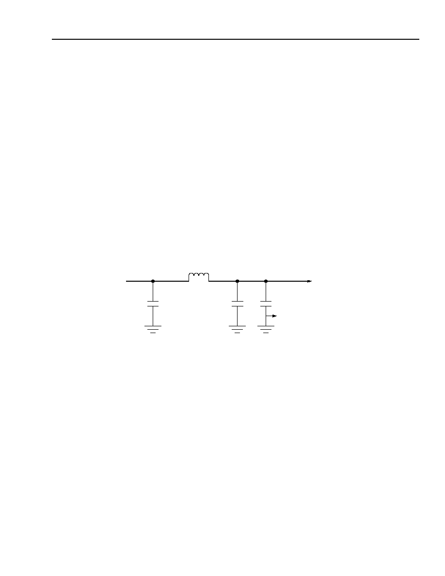
Agere Systems Inc.
33
Data Sheet
October 2001
10 Gbits/s, and 12.5 Gbits/s Line Interface FPSC
ORCA ORLI10G Quad 2.5 Gbits/s
Line Interface Circuit Specifications
Power Supply Decoupling LC Circuit
The 622 MHz--850 MHz line interface macro contains both analog and digital circuitry. The line interface function,
for example, is implemented as primarily a digital function, but it relies on a conventional analog phase-locked loop
to provide its divided clocks. The internal analog phase-locked loop contains a voltage-controlled oscillator. This
circuit will be sensitive to digital noise generated from the rapid switching transients associated with internal logic
gates and parasitic inductive elements. Generated noise that contains frequency components beyond the band-
width of the internal phase-locked loop (about 3 MHz) will not be attenuated by the phase-locked loop and will
impact bit error rate directly. Thus, separate power supply pins are provided for these critical analog circuit ele-
ments.
Additional power supply filtering in the form of an LC pi filter section will be used between the power supply source
and these device pins as shown in Figure 16. The corner frequency of the LC filter is chosen based on the power
supply switching frequency, which is between 100 kHz and 300 kHz in most applications.
Capacitors C1 and C2 are large electrolytic capacitors to provide the basic cutoff frequency of the LC filter. For
example, the cutoff frequency of the combination of these elements might fall between 5 kHz and 50 kHz. Capaci-
tor C3 is a smaller ceramic capacitor designed to provide a low-impedance path for a wide range of high-frequency
signals at the analog power supply pins of the device. The physical location of capacitor C3 must be as close to the
device lead as possible. Multiple instances of capacitors C3 can be used if necessary. The recommended filter for
the HSI macro is shown below: L = 4.7
µ
H, RL = 1
, C1 = 0.01
µ
F, C2 = 0.01
µ
F, C3 = 4.7
µ
F.
5-9344(F).a
Figure 16. Sample Power Supply Filter Network for Analog LI Power Supply Pins
C2
+
C3
+
TO DEVICE
V
DD
33, V
DD
33_A[7:4]
V
SS
, V
SS
33_A[7:4]
C1
+
FROM POWER
SUPPLY SOURCE
L
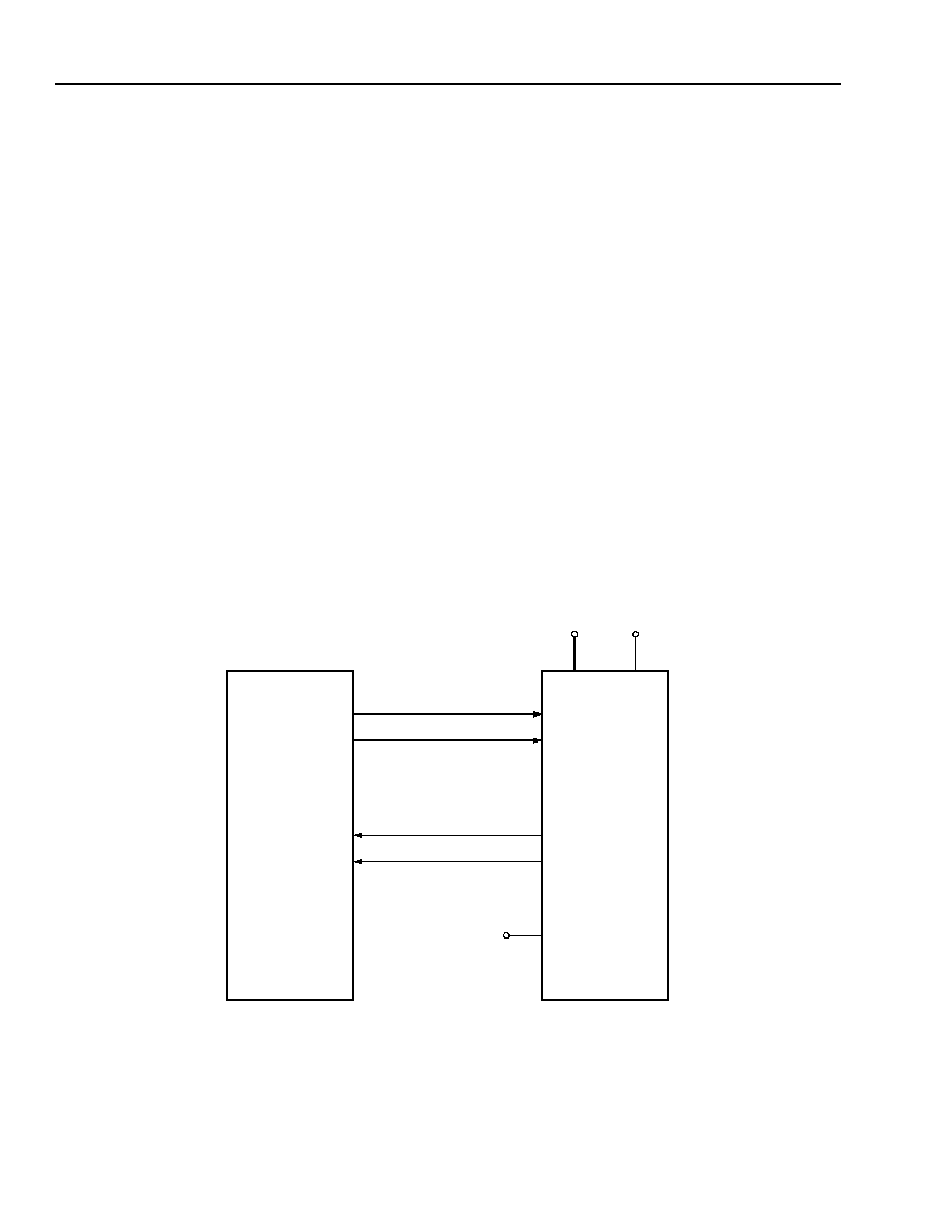
34
Agere Systems Inc.
Data Sheet
October 2001
10 Gbits/s, and 12.5 Gbits/s Line Interface FPSC
ORCA ORLI10G Quad 2.5 Gbits/s
XGMII ORCA 4E Receive Analysis
XGMII Considerations
The stringent 10 Gbit media independent interface specifications from the IEEE 802.3ae standards are met in the
FPGA side of the ORLI10G device. Figure 17 and Table 4 show a simplified block diagram for this interface and the
receive voltage levels for the HSTL inputs to the ORLI10G device. Further details are available in the Series 4 I/O
application note.
The ORLI10G device meets the 480 ps input setup
time and 480 ps input hold
time requirements for the XGMII
receiver inputs into the FPGA side of the FPSC with the embedded IO DDR cells on the FPGA side of the FPSC.
The PLLs are not used on input due to this being a forward clocked interface. The ORLI10G meets the clock-to-out
specification on the XGMII DDR outputs by using the output shift register to produce a nonduty cycle-dependent
output. An embedded output DDR capability is also available. The output clock is then centered around this data
eye using internal PLLs.
There are two considerations to note about the pinout location of the XGMII input clocks:
1. The XGMII input clocks must be located at the C pad of the programmable I/O cells (PICs). In the pinout tables,
the pads are labeled on a pin-by-pin basis. For example, a pin whose pad is referenced as PL1C can be used
as an XGMII input clock, but pins referenced as PL1A, PL1B, or PL1D cannot be used as an XGMII input clock.
2. The XGMII input data pins can be no further then six PICs away from the XGMII input clock pin. This means
that in the 416 PBGA package, the clock needs to be driven on two pins to be able to clock in the 32-bit XGMII
input data bus.
Due to the strict pinout locations mentioned above, when implementing a XGMII interface, the microprocessor
interface (MPI) will not be available in the 416 PBGA package.
1550.a(F)
Figure 17. Simplified XGMII Block Diagram
HSTL
CLOCK
CLOCK
V
DDIO
V
DD15
V
DDIO
= 1.5 V NOM
HSTL
V
DDIO
= 1.5 V NOM
V
REF
V
DDIO
˜
2
DDR DATA
DDR DATA
CUSTOMER DEVICE
ORLI10G
SY
ST
EM
I
N
T
E
R
F
AC
E
LI
NE
INTE
RFA
C
E
Agere Systems Inc.
35
Data Sheet
October 2001
10 Gbits/s, and 12.5 Gbits/s Line Interface FPSC
ORCA ORLI10G Quad 2.5 Gbits/s
XGMII ORCA 4E Receive Analysis
(continued)
Table 4. HSTL Input Requirements to FPGA
Absolute Maximum Ratings
Stresses in excess of the absolute maximum ratings can cause permanent damage to the device. These are abso-
lute stress ratings only. Functional operation of the device is not implied at these or any other conditions in excess
of those given in the operations sections of this data sheet. Exposure to absolute maximum ratings for extended
periods can adversely affect device reliability.
The ORCA Series 4 FPSCs include circuitry designed to protect the chips from damaging substrate injection cur-
rents and to prevent accumulations of static charge. Nevertheless, conventional precautions should be observed
during storage, handling, and use to avoid exposure to excessive electrical stress.
Table 5. Absolute Maximum Ratings
Recommended Operating Conditions
Table 6. Recommended Operating Conditions
Notes:
The maximum recommended junction temperature (T
J
) during operation is 125 ∞C.
Timing parameters in this data sheet and ORCA Foundry are characterized under tighter voltage and temperature conditions than the
recommended operating conditions in this table.
The internal PLLs operate from the V
DD
33 and V
DD
33_A power supplies. These power supplies should be well isolated from all other power
supplies on the board for proper operation.
Inputs
Low
Nom
High
V
DDIO
1.4 V
1.5 V
1.6 V
V
IH
(min level)
0.88 V
0.95 V
1.10 V
V
REF
0.68 V
0.75 V
0.90 V
V
IL
(max level)
0.48 V
0.55 V
0.70 V
Parameter
Symbol
Min
Max
Unit
Storage Temperature
T
stg
≠65 150 ∞C
Power Supply Voltage with Respect to Ground
V
DD
33
≠0.3
4.2
V
V
DDIO
≠0.3
4.2
V
V
DD
33, V
DD
33_A
≠0.3
2.0
V
V
DD
15
≠0.3
2.0
V
Input Signal with Respect to Ground
V
IN
≠0.3
V
DDIO
+ 0.3
V
Signal Applied to High-impedance Output
--
≠0.3
V
DDIO
+ 0.3
V
Maximum Package Body Temperature
--
--
220
∞C
Parameter
Symbol
Min
Max
Unit
Power Supply Voltage with Respect to Ground
V
DD
33
2.7
3.6
V
V
DDIO
1.4
3.6
V
V
DD
33, V
DD
33_A
1.4
1.6
V
V
DD
15
1.4
1.6
V
Input Voltages
V
IN
≠0.3
V
DDIO
+ 0.3
V
Junction Temperature
T
J
≠40
125
∞C
36
Agere Systems Inc.
Data Sheet
October 2001
10 Gbits/s, and 12.5 Gbits/s Line Interface FPSC
ORCA ORLI10G Quad 2.5 Gbits/s
Embedded Core LVDS I/O
Table 7. Driver dc Data*
* V
DD
33 = 3.1 V--3.5 V, V
DD
15 = 1.4 V--1.6 V, ≠40 ∞C, and slow-fast process.
External reference, REF10 = 1.0 V ± 3%, REF14 = 1.4 V ± 3%.
Table 8. Driver ac Data*
* V
DD
33 = 3.1 V--3.5 V, V
DD
15 = 1.4 V--1.6 V, ≠40 ∞C, and slow-fast process.
Table 9. Driver Power Consumption*
* V
DD
33 = 3.1 V--3.5 V, V
DD
15 = 1.4 V--1.6 V, ≠40 ∞C, and slow-fast process.
Parameter
Symbol
Test Conditions
Min
Typ
Max
Unit
Output Voltage High, V
OA
or V
OB
V
OH
R
LOAD
= 100
± 1%
--
--
1.475
V
Output Voltage Low, V
OA
or V
OB
V
OL
R
LOAD
= 100
± 1%
0.925
--
--
V
Output Differential Voltage
V
OD
R
LOAD
= 100
± 1%
0.25
--
0.45
V
Output Offset Voltage
V
OS
R
LOAD
= 100
± 1%
1.125*
--
1.275
V
Output Impedance, Differential
R
o
V
CM
= 1.0 V and 1.4 V
80
100
120
R
O
Mismatch Between A and B
R
O
V
CM
= 1.0 V and 1.4 V
--
--
10
%
Change in Differential Voltage Between
Complementary States
V
OD
R
LOAD
= 100
± 1%
--
--
25
mV
Change in Output Offset Voltage
Between Complementary States
V
OS
R
LOAD
= 100
± 1%
--
--
25
mV
Output Current
I
SA,
I
SB
Driver shorted to GND
--
--
24
mA
Output Current
I
SAB
Drivers shorted together
--
--
12
mA
Power-off Output Leakage
|Ixa|, |Ixb|
V
DD
= 0 V
V
PAD
, V
PADN
= 0 V--2.5 V
--
--
10
mA
Parameter
Symbol
Test Conditions
Min
Max
Unit
V
OD
Fall Time, 80% to 20%
t
F
Z
L
= 100
± 1%
C
PAD
= 3.0 pF, C
PAD
= 3.0 pF
100
210
ps
V
OD
Rise Time, 20% to 80%
t
R
Z
L
= 100
± 1%
C
PAD
= 3.0 pF, C
PAD
= 3.0 pF
100
210
ps
Differential Skew:
|t
PHLA
≠ t
PLHB
| or
|t
PHLB
≠ t
PLHA
|
t
SKEW1
Any differential pair on package at 50% point of
the transition
--
50
ps
Channel-to-channel Skew:
|tpDIFFm ≠ tpDIFFn|
t
SKEW2
Any two signals on package at 0 V differential
--
--
ps
Propagation Delay Time
t
PLH
t
PHL
Z
L
= 100
± 1%
C
PAD
= 3.0 pF, C
PADN
= 3.0 pF
0.54
0.55
1.10
1.09
ns
ns
Parameter
Symbol
Test Conditions
Min
Max
Unit
Driver dc Power
PD
dc
Z
L
= 100
± 1%
--
26.0
mW
Driver ac Power
PD
ac
Z
L
= 100
± 1%
C
PAD
= 3.0 pF, C
PADN
= 3.0 pF
--
64
µW/MHz
Agere Systems Inc.
37
Data Sheet
October 2001
10 Gbits/s, and 12.5 Gbits/s Line Interface FPSC
ORCA ORLI10G Quad 2.5 Gbits/s
Embedded Core LVDS I/O
(continued)
LVDS Receiver Buffer Requirements
Table 10. Receiver ac Data*
* V
DD
= 3.1 V--3.5 V, 0 ∞C --125 ∞C, slow-fast process.
Table 11. Receiver Power Consumption*
* V
DD
= 3.1 V--3.5 V, 0 ∞C --125 ∞C, slow-fast process.
Table 12. Receiver dc Data*
* V
DD
= 3.1 V--3.5 V, 0 ∞C --125 ∞C, slow-fast process.
External reference, REF10 = 1.0 V ± 3%, REF14 = 1.4 V ± 3%.
Table 13. LVDS Operating Parameters
Note: Under worst-case operating condition, the LVDS driver will withstand a disabled or unpowered receiver for an unlimited period of time
without being damaged. Similarly, when outputs are short-circuited to each other or to ground, the LVDS will not suffer permanent dam-
age. The LVDS driver supports hot insertion. Under a well-controlled environment, the LVDS I/O can drive backplane as well as cable.
Parameter
Symbol
Test Conditions
Min
Max
Unit
Pulse-width Distortion
t
pwd
V
IDTH
= 100 mV, 311 MHz
--
160
ps
Propagation Delay Time
t
PLH
t
PHL
C
L
= 0.5 pF
0.60
0.60
1.42
1.47
ns
ns
With Common-mode Variation (0 V to 2.4 V)
t
PD
C
L
= 0.5 pF
--
50
ps
Output Rise Time, 20% to 80%
t
R
C
L
= 0.5 pF
150
350
ps
Output Fall Time, 80% to 20%
t
F
C
L
= 0.5 pF
150
350
ps
Parameter
Symbol
Test Conditions
Min
Max
Unit
Receiver dc Power
P
Rdc
dc
--
20.4
mW
Receiver ac Power
P
Rac
ac
C
L
= 1.5 pF
--
4.5
µW/MHz
Parameter
Symbol
Test Conditions
Min
Typ
Max
Unit
Input Voltage Range, VIA or VIB
V
I
V
GPD
< 925 mV
dc ≠ 1 MHz
0.0
1.2
2.4
V
Input Differential Threshold
V
IDTH
V
GPD
< 925 mV
400 MHz
≠100
--
100
mV
Input Differential Hysteresis
V
HYST
(+V
IDTHH
) ≠ (≠V
IDTHL
)
--
--
--
mV
Receiver Differential Input Impedance
R
IN
With build-in termination,
center-tapped
80
100
120
Parameter
Test Conditions
Min
Normal
Max
Unit
Transmit Termination Resistor
--
80
100
120
Receiver Termination Resistor
--
80
100
120
Temperature Range
--
≠40
--
125
∞C
Power Supply V
DD
33
--
3.1
--
3.5
V
Power Supply V
DD
15
--
1.4
--
1.6
V
Power Supply V
SS
--
--
0
--
V
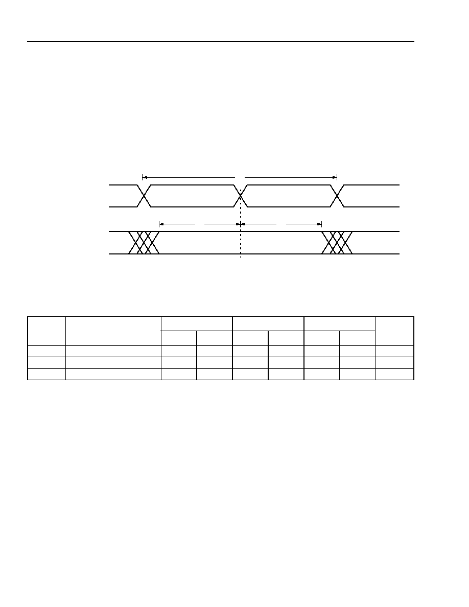
38
Agere Systems Inc.
Data Sheet
October 2001
10 Gbits/s, and 12.5 Gbits/s Line Interface FPSC
ORCA ORLI10G Quad 2.5 Gbits/s
Timing Characteristics
Receive Input Data Interface
Receive STS-48/STS-192 (2.5G/10G) Data Inputs
Figure 18 illustrates the timing for the receive STS-48/STS-192 data stream. Both the clock and data pins are low-
voltage differential signal (LVDS) input buffers. The expected clock rate is 622 MHz--850 MHz, and the receive
data is clocked on the rising edge of the clock. In 2.5G mode, each of the four channels uses one set of
RX_CLK_INn and 4 RX_DAT_INn data pins. In 10G mode, only RX_CLK_IN0 is used, along with the
RX_DAT_IN[15:0] pins.
5-9085.b (F)
Figure 18. Receive Input Data Timing
Table 14. Receive Data Input Timing
It is recommended that the Rx clock be inverted by crossing the LVDS pin pair, that is, connect the N to the P and
the P to the N. This is because the embedded LI requires the Rx data to be centered on the Rx clock, and typically
the devices that drive the ORLI10G transmit clock and data on the same clock edge. The timing values for the
diagram are given in Table 14.
Symbol
Parameter
≠1
≠2
≠3
Unit
Min
Max
Min
Max
Min
Max
t1
Clock Frequency
--
667
--
790
--
850
MHz
t2
Data Setup Time Required
300
--
225
--
210
--
ps
t3
Data Hold Time Required
300
--
225
--
210
--
ps
RX_CLK_IN_[3:0]
RX_DATA_IN_[15:0]
P
N
P
N
t1
t3
t2
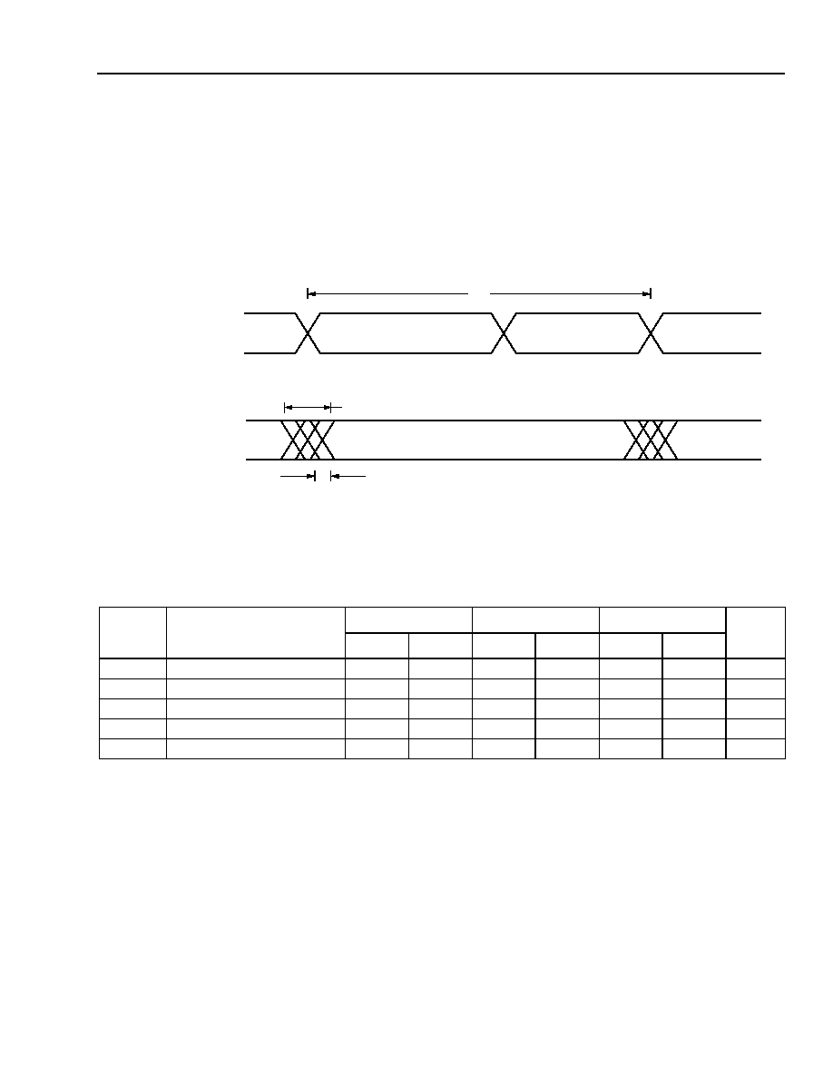
Agere Systems Inc.
39
Data Sheet
October 2001
10 Gbits/s, and 12.5 Gbits/s Line Interface FPSC
ORCA ORLI10G Quad 2.5 Gbits/s
Timing Characteristics
(continued)
Transmit STS-48/STS-192 (2.5G/10G) Data Outputs
Figure 19 illustrates the timing for the transmit STS-48/STS-192 data stream. Both the clock and data pins are
driven with low-voltage differential signal (LVDS) output buffers. The expected clock rate is 622 MHz--850 MHz
and the transmit data is clocked out on the rising edge of the clock. In 2.5G mode, each of the four channels uses
one set of TX_CLK_OUTn with four TX_DAT_OUTn data pins. In 10G mode, only TX_CLK_OUT[0] is used with
the 16 TX_DAT_OUT[15:0] pins. The timing values for the diagram are given in Table 15.
5-9089.c(F)
Figure 19. Transmit Output Data Timing
Table 15. Transmit Data Output Timing
* This requirement is for all sources of the output clocks (e.g., RCLKSI, etc.).
It is recommended that the Tx clock be inverted by crossing the LVDS pin pair, that is, connect the N to the P and
the P to the N. This is because the receiving device that will be driven by the ORLI10G typically requires that data
be centered around the clock, but the ORLI10G drives both the clock and data from the same clock edge.
Symbol
Parameter
≠1
≠2
≠3
Unit
Min
Max
Min
Max
Min
Max
t4
Clock Frequency
--
667
--
790
--
850
MHz
--
Duty Cycle
45
55
45
55
45
55
%
t5
Data Delay from Clock Edge
≠300
300
≠225
225
≠210
210
ps
t6
Data Rise Time: 20%--80%
100
200
100
200
100
200
ps
t7
Data Fall Time: 80%--20%
100
200
100
200
100
200
ps
t5
TX_DAT_OUT[15:0]
P
N
P
N
t6
t7
TX_CLK_OUT[3:0]
t4
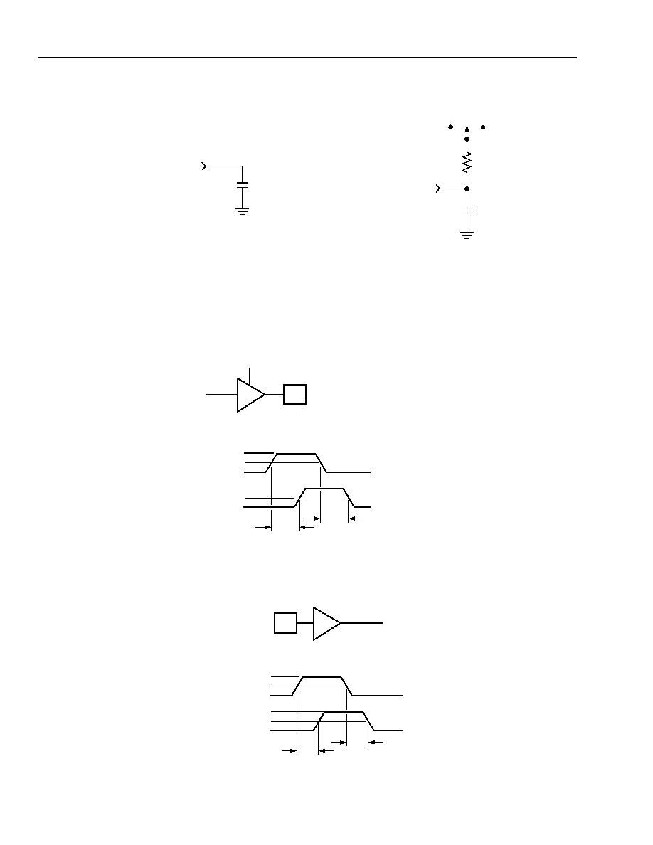
40
Agere Systems Inc.
Data Sheet
October 2001
10 Gbits/s, and 12.5 Gbits/s Line Interface FPSC
ORCA ORLI10G Quad 2.5 Gbits/s
Input/Output Buffer Measurement Conditions (Non-LVDS Buffer)
Note: Switch to V
DD
for
T
PLZ
/T
PZL
; switch to GND for T
PHZ
/T
PZH
.
5-3234(F)
Figure 20. ac Test Loads
5-3233.a(F)
Figure 21. Output Buffer Delays
5-3235(F)
Figure 22. Input Buffer Delays
50 pF
A. Load Used to Measure Propagation Delay
TO THE OUTPUT UNDER TEST
TO THE OUTPUT UNDER TEST
50 pF
V
CC
GND
1 k
B. Load Used to Measure Rising/Falling Edges
V
DD
T
PHH
V
DD
/2
V
SS
out[i]
PAD
OUT
1.5 V
0.0 V
T
PLL
PAD
out[i]
ac TEST LOADS (SHOWN ABOVE)
ts[i]
OUT
0.0 V
1.5 V
T
PHH
T
PLL
PAD
in[i]
IN
3.0 V
V
SS
V
DD
/2
V
DD
PAD IN
in[i]
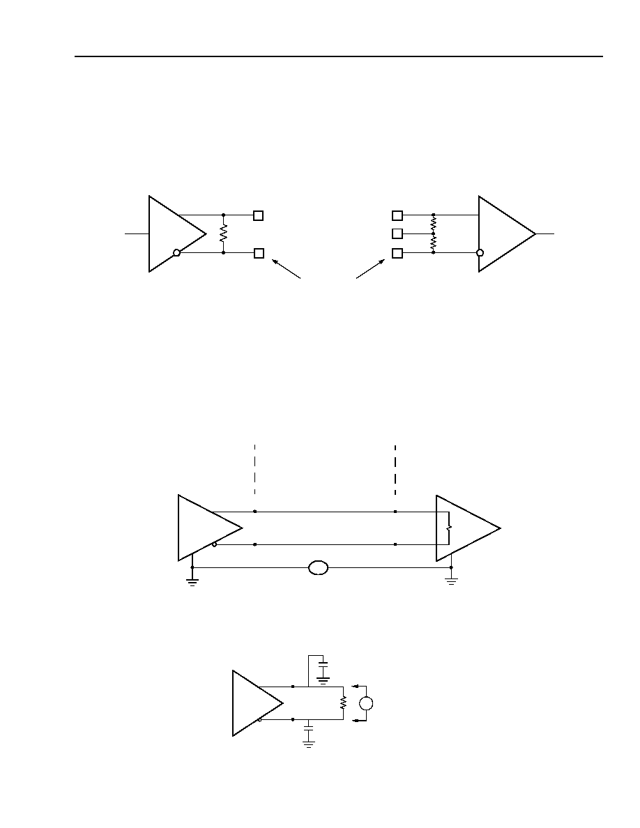
Agere Systems Inc.
41
Data Sheet
October 2001
10 Gbits/s, and 12.5 Gbits/s Line Interface FPSC
ORCA ORLI10G Quad 2.5 Gbits/s
LVDS Buffer Characteristics
Termination Resistor
The LVDS drivers and receivers operate on a 100
differential impedance, as shown below. External resistors are
not required. The differential driver and receiver buffers include termination resistors inside the device package, as
shown in Figure 23.
5-8703(F)
Figure 23. LVDS Driver and Receiver and Associated Internal Components
LVDS Driver Buffer Capabilities
Under worst-case operating condition, the LVDS driver must withstand a disabled or unpowered receiver for an
unlimited period of time without being damaged. Similarly, when its outputs are short-circuited to each other or to
ground, the LVDS driver will not suffer permanent damage. Figure 24 illustrates the terms associated with LVDS
driver and receiver pairs.
5-8704(F)
Figure 24. LVDS Driver and Receiver
5-8705(F)
Figure 25. LVDS Driver
LVDS DRIVER
50
50
LVDS RECEIVER
CENTER TAP
DEVICE PINS
100
EXTERNAL
V
GPD
V
OA
V
OB
V
IA
V
IB
A
B
AA
BB
DRIVER INTERCONNECT
RECEIVER
V
OA
A
V
OB
B
C
A
C
B
R
LOAD
V
OD
= (V
OA
≠ V
OB
)
V
42
Agere Systems Inc.
Data Sheet
October 2001
10 Gbits/s, and 12.5 Gbits/s Line Interface FPSC
ORCA ORLI10G Quad 2.5 Gbits/s
Pin Information
This section describes the pins and signals that perform FPGA-related functions. During configuration, the user-
programmable I/Os are 3-stated and pulled up with an internal resistor. If any FPGA function pin is not used (or not
bonded to package pin), it is also 3-stated and pulled up after configuration.
Table 16. FPGA Common-Function Pin Description
Symbol
I/O
Description
Dedicated Pins
V
DD
33
-- 3 V positive power supply.
V
DD
15
-- 1.5 V positive power supply for internal logic.
V
DDIO
-- Positive power supply used by I/O banks.
GND
-- Ground supply.
PTEMP
I
Temperature-sensing diode pin. Dedicated input.
RESET
I
During configuration,
RESET
forces the restart of configuration and a pull-up is enabled.
After configuration,
RESET
can be used as a general FPGA input or as a direct input,
which causes all PLC latches/FFs to be asynchronously set/reset.
CCLK
I
O
In the master and asynchronous peripheral modes, CCLK is an output which strobes con-
figuration data in. In the slave or readback after configuration, CCLK is input synchronous
with the data on DIN or D[7:0]. CCLK is an output for daisy-chain operation when the lead
device is in master, peripheral, or system bus modes.
DONE
I
As an input, a low level on DONE delays FPGA start-up after configuration.*
O
As an active-high, open-drain output, a high level on this signal indicates that configura-
tion is complete. DONE has an optional pull-up resistor.
PRGM
I
PRGM
is an active-low input that forces the restart of configuration and resets the bound-
ary-scan circuitry. This pin always has an active pull-up.
RD_CFG
I
This pin must be held high during device initialization until the
INIT
pin goes high. This pin
always has an active pull-up.
During configuration,
RD_CFG
is an active-low input that activates the TS_ALL function
and 3-states all of the I/O.
After configuration,
RD_CFG
can be selected (via a bit stream option) to activate the
TS_ALL function as described above, or, if readback is enabled via a bit stream option, a
high-to-low transition on
RD_CFG
will initiate readback of the configuration data, including
PFU output states, starting with frame address 0.
RD_DATA/TDO
O
RD_DATA/TDO is a dual-function pin. If used for readback, RD_DATA provides configu-
ration data out. If used in boundary-scan, TDO is test data out.
CFG_IRQ/MPI_IRQ
O
During JTAG, slave, master, and asynchronous peripheral configuration assertion on this
CFG_IRQ
(active-low) indicates an error or errors for block RAM or FPSC initialization.
MPI
active-low interrupt request output.
* The FPGA States of Operation section in the ORCA Series 4 data sheet contains more information on how to control these signals during
start-up. The timing of DONE release is controlled by one set of bit stream options, and the timing of the simultaneous release of all other con-
figuration pins (and the activation of all user I/Os) is controlled by a second set of options.
Agere Systems Inc.
43
Data Sheet
October 2001
10 Gbits/s, and 12.5 Gbits/s Line Interface FPSC
ORCA ORLI10G Quad 2.5 Gbits/s
Pin Information
(continued)
Figure 16. FPGA Common-Function Pin Description (continued)
Symbol
I/O
Description
Special-Purpose Pins (Can also be used as a general I/O.)
M[3:0]
I
During powerup and initialization, M0--M3 are used to select the configuration mode with
their values latched on the rising edge of INIT. During configuration, a pull-up is enabled.
I/O After configuration, these pins are user-programmable I/O.*
PLL_CK[0:1,6:7]
I/O Dedicated PCM clock pins. These pins are a user-programmable I/O pins if not used by
PLLs.
P[TBLR]CLK[1:0]
[TC]
I/O Pins dedicated for the primary clock. These are input pins on the middle of each side with
differential pairing. They may be used as general I/O pins if not needed for clocking pur-
poses.
TDI, TCK, TMS
I
If boundary-scan is used, these pins are test data in, test clock, and test mode select
inputs. If boundary-scan is not selected, all boundary-scan functions are inhibited once con-
figuration is complete. Even if boundary-scan is not used, either TCK or TMS must be held
at logic 1 during configuration. Each pin has a pull-up enabled during configuration.
I/O After configuration, these pins are user-programmable I/O.*
RDY/BUSY/RCLK
O
During configuration in peripheral mode, RDY/RCLK indicates another byte can be written
to the FPGA. If a read operation is done when the device is selected, the same status is
also available on D7 in asynchronous peripheral mode.
After configuration, if the MPI is not used, this pin is a user-programmable I/O pin.*
I/O During the master parallel configuration mode, RCLK is a read output signal to an external
memory. This output is not normally used.
HDC
O
High during configuration is output high until configuration is complete. It is used as a con-
trol output, indicating that configuration is not complete.
I/O After configuration, this pin is a user-programmable I/O pin.*
LDC
O
Low during configuration is output low until configuration is complete. It is used as a control
output, indicating that configuration is not complete.
I/O After configuration, this pin is a user-programmable I/O pin.*
INIT
I/O INIT is a bidirectional signal before and during configuration. During configuration, a pull-up
is enabled, but an external pull-up resistor is recommended. As an active-low, open-drain
output, INIT is held low during power stabilization and internal clearing of memory. As an
active-low input, INIT holds the FPGA in the wait-state before the start of configuration.
After configuration, this pin is a user-programmable I/O pin.*
CS0, CS1
I
CS0 and CS1 are used in the asynchronous peripheral, slave parallel, and microproces-
sor configuration modes. The FPGA is selected when CS0 is low and CS1 is high. During
configuration, a pull-up is enabled.
I/O After configuration, these pins are user-programmable I/O pins.*
RD/MPI_STRB
I
RD is used in the asynchronous peripheral configuration mode. A low on RD changes D7
into a status output. As a status indication, a high indicates ready, and a low indicates
busy. WR and RD should not be used simultaneously. If they are, the write strobe over-
rides. This pin is also used as the MPI data transfer strobe.
I/O After configuration, if the MPI is not used, this pin is a user-programmable I/O pin.*
* The FPGA States of Operation section in the ORCA Series 4 data sheet contains more information on how to control these signals during
start-up. The timing of DONE release is controlled by one set of bit stream options, and the timing of the simultaneous release of all other con-
figuration pins (and the activation of all user I/Os) is controlled by a second set of options.
44
Agere Systems Inc.
Data Sheet
October 2001
10 Gbits/s, and 12.5 Gbits/s Line Interface FPSC
ORCA ORLI10G Quad 2.5 Gbits/s
Pin Information
(continued)
Figure 16. FPGA Common-Function Pin Description (continued)
Symbol
I/O
Description
A[17:0]
MPI_BURST
MPI_BDIP
MPI_TSZ[1:0]
A[21:0]
I
During MPI mode, the A[17:0] are used as the address bus driven by the PowerPC bus
master utilizing the least significant bits of the PowerPC 32-bit address.
O
During master parallel configuration mode, A[17:0] address the configuration EPROM. In
MPI mode, many of the A[n] pins have alternate uses as described below. See the special
function blocks section for more MPI information. During configuration, if not in master par-
allel or an MPI configuration mode, these pins are 3-stated with a pull-up enabled.
A[21] is used as the MPI_BURST. It is driven low to indicate a burst transfer is in progress.
Driven high indicates that the current transfer is not a burst.
A[20] is used as the MPI_BDIP. It is driven by the PowerPC processor; assertion of this pin
indicates that the second beat in front of the current one is requested by the master.
Negated before the burst transfer ends to abort the burst data phase.
A[19:18] are used as the MPI_TSZ[1:0] signals and are driven by the bus master to indicate
the data transfer size for the transaction. Set 01 for byte, 10 for half-word, and 00 for word.
During master parallel mode A[21:0], address the configuration EPROMs up to 4 Mbytes.
If not used for MPI, these pins are user-programmable I/O pins.*
MPI_ACK
O
In PowerPC mode MPI operation, this is driven low indicating the MPI received the data on
the write cycle or returned data on a read cycle.
MPI_CLK
I
This is the PowerPC synchronous, positive-edge bus clock used for the MPI interface. It
can be a source of the clock for the embedded system bus. If MPI is used, this can be the
AMBA bus clock.
MPI_TEA
O
A low on the MPI transfer error acknowledge indicates that the MPI detects a bus error on
the internal system bus for the current transaction.
MPI_RTRY
O
This pin requests the MPC860 to relinquish the bus and retry the cycle.
D[31:0]
I/O Selectable data bus width from 8-, 16-, 32-bit. Driven by the bus master in a write transac-
tion. Driven by MPI in a read transaction.
I
D[7:0] receive configuration data during master parallel, peripheral, and slave parallel con-
figuration modes and each pin has a pull-up enabled. During serial configuration modes,
D0 is the DIN input.
D[7:3] output internal status for asynchronous peripheral mode when RD is low.
After configuration, the pins are user-programmable I/O pins.*
DP[3:0]
I/O Selectable parity bus width from 1, 2, 4-bit, DP[0] for D[7:0], DP[1] for D[15:8], DP[2] for
D[23:16], and DP[3] for D[32:24].
After configuration, this pin is a user-programmable I/O pin.*
DIN
I
During slave serial or master serial configuration modes, DIN accepts serial configuration
data synchronous with CCLK. During parallel configuration modes, DIN is the D0 input.
During configuration, a pull-up is enabled.
I/O After configuration, this pin is a user-programmable I/O pin.*
DOUT
O
During configuration, DOUT is the serial data output that can drive the DIN of daisy-chained
slave devices. Data out on DOUT changes on the rising edge of CCLK.
I/O After configuration, DOUT is a user-programmable I/O pin.*
* The FPGA States of Operation section in the ORCA Series 4 data sheet contains more information on how to control these signals during
start-up. The timing of DONE release is controlled by one set of bit stream options, and the timing of the simultaneous release of all other con-
figuration pins (and the activation of all user I/Os) is controlled by a second set of options.

Agere Systems Inc.
45
Data Sheet
October 2001
10 Gbits/s, and 12.5 Gbits/s Line Interface FPSC
ORCA ORLI10G Quad 2.5 Gbits/s
Pin Information
(continued)
This table describes the I/O signal ports on the embedded core portion of the device.
Table 17. FPSC Function Pin Description
Symbol
I/O
Description
Control and Global Pins
PLL_BYPASS
I
3.3 V active-high. Enables the bypass mode for both receive and both transmit
PLLs.
PWRDN
I
3.3 V active-high. Power down all LVDS links and both receive and both transmit
PLLs.
RESET_RX
I
3.3 V active-high. Resets the receive PLLs and the demultiplexer block.
RESET_TX
I
3.3 V active-high. Resets the transmit PLLs and the multiplexer block.
Receive I/O Pins
RX_DAT_IN_N<15:0>
I
LVDS data input for receive side.
RX_DAT_IN_P<15:0>
I
LVDS data input for receive side.
RX_CLK_IN_N<3:0>
I
LVDS clock inputs for receive side.
RX_CLK_IN_P<3:0>
I
LVDS clock inputs for receive side.
Transmit I/O Pins
TX_DAT_OUT_N<15:0>
O
LVDS data outputs on transmit side.
TX_DAT_OUT_N<15:0>
O
LVDS data outputs on transmit side.
TX_CLK_OUT_N<3:0>
O
LVDS clock outputs on transmit side.
TX_CLK_OUT_N<3:0>
O
LVDS clock outputs on transmit side.
TX_CLK_IN_N
I
LVDS transmit reference clock input.
TX_CLK_IN_P
I
LVDS transmit reference clock input.
LVDS Input Reference Pins
LV_REF10
--
LVDS reference voltage: 1.0 V ± 3%.
LV_REF14
--
LVDS reference voltage: 1.4 V ± 3%.
LV_RESHI
--
LVDS resistor high pin (use 100
to LV_RESLO pin).
LV_RESLO
--
LVDS resistor low pin (use 100
to LV_RESHI pin).
LVCTAP_[6:1]
--
LVDS input centertap (use 0.01 µF to GND).
46
Agere Systems Inc.
Data Sheet
October 2001
10 Gbits/s, and 12.5 Gbits/s Line Interface FPSC
ORCA ORLI10G Quad 2.5 Gbits/s
Pin Information
(continued)
In
Figure 18, an output refers to a signal flowing into the FGPA logic (out of the embedded core) and an input refers
to a signal flowing out of the FPGA logic (into the embedded core).
Table 18. Embedded Core/FPGA Interface Signal Description
Pin Name
I/O
Description
Receive Signals
RX_DAT_OUT<127:0>
O
Data from demultiplexer on receive side.
RX_CLK8_OUT<3:0>
O
Divided down clocks on receive side.
RX_ENB8_OUT<3:0>
O
Data enables on receive side.
RX1_VCOP
O
RX1_PLL output clock on receive side (M/N clock) after phase select.
RX1_VCO
O
RX1_PLL output clock on receive side (M/N clock) before phase select.
RX2_VCOP
O
RX2_PLL output clock on receive side (x1 clock) after phase select.
RX2_VCO
O
RX2_PLL output clock on receive side (x1 clock) before phase select.
RX2_FBCKI
I
PLL feedback input to RX2_PLL. This allows for the removal of the
FPGA clock routing delay.
RX1_BYPASS
I
Set to 1 to bypass the RX1 PLL.
RX2_BYPASS
I
Set to 1 to bypass the RX2 PLL.
RX_LOCK
O
Lock signal for RX1_PLL and RX2_PLL. This signal is a logical OR of
the lock signal from both PLLs. It is not integrated; thus, small glitches
can occur on this signal during normal PLL operation.
Transmit Signals
TX_DAT_IN<127:0>
I
Data to multiplexer on transmit side.
TX_CLK8_IN<3:0>
I
Clocks to multiplexer on transmit side.
TX_ENB8_IN[3:0]
I
Data enables on transmit side.
TX1_VCOP
O
TX1_PLL output clock on transmit side (M/N clock) after phase select.
TX1_VCO
O
TX1_PLL output clock on transmit side (M/N clock) before phase select.
TX2_VCOP
O
TX2_PLL output clock on transmit side (x1 clock) after phase select.
TX2_VCO
O
TX2_PLL output clock on transmit side (x1 clock) before phase select.
TX2_FBCKI
I
PLL feedback input to TX2 PLL. This allows for the removal of the
FPGA clock routing delay.
TX1_BYPASS
I
Set to 1 to bypass the TX1 PLL.
TX2_BYPASS
I
Set to 1 to bypass the TX2 PLL.
TX_LOCK
O
Lock signal for TX1_PLL and TX2_PLL. This signal is a logical OR of
the lock signal from both PLLs. It is not integrated; thus, small glitches
can occur on this signal during normal PLL operation.
Vss_A<7:4>
--
Analog ground for the embedded line interface PLLs.
V
DD
33_A<7:4>
--
Analog power supply for the embedded line interface PLLs.

Agere Systems Inc.
47
Data Sheet
October 2001
10 Gbits/s, and 12.5 Gbits/s Line Interface FPSC
ORCA ORLI10G Quad 2.5 Gbits/s
Pin Information
(continued)
Package Pinouts
Table 14 provides the number of user programmable I/Os available for each available package. Table 20 provides
the package pin and pin function for the ORLI10G FPSC and packages. The bond pad name is identified in the
PIO nomenclature used in the ORCA Foundry design editor. The bank column provides information as to which
output voltage level bank the given pin is in. The group column provides information as to the group of pins the
given pin is in. This is used to show which V
REF
pin is used to provide the reference voltage for single-ended
limited-swing I/Os. If none of these buffer types (such as SSTL, GTL, HSTL) are used in a given group, then the
V
REF
pin is available as an I/O pin.
When the number of FPGA bond pads exceeds the number of package pins, bond pads are unused. When the
number of package pins exceeds the number of bond pads, package pins are left unconnected (no connects).
When a package pin is to be left as a no connect for a specific die, it is indicated as a note in the device column for
the FPGA. The tables provide no information on unused pads.
Table 19. ORCA Programmable I/Os Summary
It is very important to note the pinout limitations for 10 Gbits/s Ethernet applications. Specifically, the very stringent
timing requirements of the XGMII specification coupled with the I/O availability and locations in the 416-pin PBGA
requires that the XGMII output pins be located on three sides of the device. This may cause issues with routing the
XGMII bus at a board level since the XGMII specification for routing this bus on a board is only 2 in.
In addition, the built-in microprocessor interface (MPI) cannot be fully utilized in the 416-pin PBGA and the 680-pin
PBGA packages because the implementation of the XGMII interface limits the number of available address and
data pins.
As shown in the Pair columns in Table 20, differential pairs and physical locations are numbered within each bank
(e.g., L19C_A0 is the nineteenth pair in an associated bank). A C indicates complementary differential whereas a
T indicates true differential. An _A0 indicates the physical location of adjacent balls in either the horizontal or verti-
cal direction. Other physical indicators are as follows:
s
_A1 indicates one ball between pairs.
s
_A2 indicates two balls between pairs.
s
_D0 indicates balls are diagonally adjacent.
s
_D1 indicates balls are diagonally adjacent separated by one physical ball.
V
REF
pins, shown in the Pin Description column in Table 20, are associated to the bank and group
(e.g., V
REF
_TL_01 is the V
REF
for group one of the top left (TL) bank).
Device
416 PBGAM
680 PBGAM
User programmable I/O
192
316
Available programmable differential pair pins
184
272
FPGA configuration pins
7
7
FPGA dedicated function pins
2
2
Core function pins
86
86
V
DD
15
28
84
V
DD
33_A
4
4
V
DD
33
14
28
V
DD
IO
21
44
V
SS
48
95
V
SS
_A
4
4
LVCTAP for dedicated differential channels
6
6
Core LV_REF pins
4
4
Total package pins
416
680

48
Agere Systems Inc.
Data Sheet
October 2001
10 Gbits/s, and 12.5 Gbits/s Line Interface FPSC
ORCA ORLI10G Quad 2.5 Gbits/s
Pin Information
(continued)
Table 20. PBGA Pinout Table
BM416 BM680
V
DD
IO
Bank
V
REF
Group
I/O
Pin Description
Additional
Function
BM416
Pair
BM680
Pair
A2
A1
--
--
Vss
Vss
--
--
--
D4
E5
--
--
V
DD
33
V
DD
33
--
--
--
D3
E4
--
--
O
PRD_DATA
RD_DATA/TDO
--
--
A1
--
--
--
V
DD
15
V
DD
15
--
--
--
C1
C1
--
--
I
PRESET_N
RESET_N
--
--
E4
D1
--
--
I
PRD_CFG_N
RD_CFG_N
--
--
F4
E2
--
--
I
PPRGRM_N
PRGRM_N
--
--
C2
A2
0 (TL)
--
V
DD
IO0
V
DD
IO0
--
--
--
D2
F4
0 (TL)
7
I/O
PL2D
PLL_CK0C/HPPLL
L14C_D0
L21C_A0
E3
F3
0 (TL)
7
I/O
PL2C
PLL_CK0T/HPPLL
L14T_D0
L21T_A0
--
A3
0 (TL)
--
V
DD
IO0
V
DD
IO0
--
--
--
--
G5
0 (TL)
7
I/O
PL3D
--
--
L22C_A0
D1
F5
0 (TL)
7
I/O
PL3C
VREF_0_07
--
L22T_A0
A25
A18
--
--
Vss
Vss
--
--
--
E2
G4
0 (TL)
7
I/O
PL4D
D5
L15C_D0
L23C_D1
F3
F2
0 (TL)
7
I/O
PL4C
D6
L15T_D0
L23T_D1
--
B1
0 (TL)
--
V
DD
IO0
V
DD
IO0
--
--
--
--
H5
0 (TL)
8
I/O
PL4B
--
--
L24C_D1
--
G3
0 (TL)
8
I/O
PL4A
VREF_0_08
--
L24T_D1
E1
F1
0 (TL)
8
I/O
PL5D
HDC
L16C_D0
L25C_A0
F2
G2
0 (TL)
8
I/O
PL5C
LDC_N
L16T_D0
L25T_A0
B1
A33
--
--
Vss
Vss
--
--
--
--
H4
0 (TL)
8
I/O
PL5B
--
--
L26C_A0
--
J5
0 (TL)
8
I/O
PL5A
--
--
L26T_A0
G4
H3
0 (TL)
9
I/O
PL6D
TESTCFG
L17C_A0
L27C_D1
H4
G1
0 (TL)
9
I/O
PL6C
D7
L17T_A0
L27T_D1
G3
B3
0 (TL)
--
V
DD
IO0
V
DD
IO0
--
--
--
F1
J4
0 (TL)
9
I/O
PL7D
VREF_0_09
L18C_D0
L28C_D1
G2
H2
0 (TL)
9
I/O
PL7C
A17/PPC_A31
L18T_D0
L28T_D1
--
A34
--
--
Vss
Vss
--
--
--
H2
K5
0 (TL)
9
I/O
PL8D
CS0_N
L19C_A0
L29C_D1
H3
J3
0 (TL)
9
I/O
PL8C
CS1
L19T_A0
L29T_D1
--
C2
0 (TL)
--
V
DD
IO0
V
DD
IO0
--
--
--
G1
H1
0 (TL)
10
I/O
PL9D
--
L20C_A0
L30C_A0
H1
J2
0 (TL)
10
I/O
PL9C
--
L20T_A0
L30T_A0
--
B2
--
--
Vss
Vss
--
--
--
--
K4
0 (TL)
10
I/O
PL9A
--
--
--
J4
L5
0 (TL)
10
I/O
PL10D
INIT_N
L21C_A0
L31C_D1
K4
K3
0 (TL)
10
I/O
PL10C
DOUT
L21T_A0
L31T_D1
A26
--
--
--
V
DD
15
V
DD
15
--
--
--
J3
J1
0 (TL)
10
I/O
PL11D
VREF_0_10
L22C_A0
L32C_A0
J2
K2
0 (TL)
10
I/O
PL11C
A16/PPC_A30
L22T_A0
L32T_A0
--
B33
--
--
Vss
Vss
--
--
--
--
K1
0 (TL)
10
I/O
PL11A
--
--
--
J1
M5
7 (CL)
1
I/O
PL12D
A15/PPC_A29
L1C_D0
L1C_A0
K2
L4
7 (CL)
1
I/O
PL12C
A14/PPC_A28
L1T_D0
L1T_A0

Agere Systems Inc.
49
Data Sheet
October 2001
10 Gbits/s, and 12.5 Gbits/s Line Interface FPSC
ORCA ORLI10G Quad 2.5 Gbits/s
K1
L1
7 (CL)
--
V
DD
IO7
V
DD
IO7
--
--
--
--
M4
7 (CL)
1
I/O
PL12B
--
--
L2C_A0
--
N5
7 (CL)
1
I/O
PL12A
--
--
L2T_A0
K3
L3
7 (CL)
1
I/O
PL13D
VREF_7_01
L2C_A0
L3C_A0
L3
L2
7 (CL)
1
I/O
PL13C
D4
L2T_A0
L3T_A0
U16
B34
--
--
Vss
Vss
--
--
--
--
N4
7 (CL)
2
I/O
PL13B
--
--
L4C_A0
--
P5
7 (CL)
2
I/O
PL13A
--
--
L4T_A0
L4
M2
7 (CL)
2
I/O
PL14D
RDY/BUSY_N/RCLK
L3C_A0
L5C_A0
M4
M1
7 (CL)
2
I/O
PL14C
VREF_7_02
L3T_A0
L5T_A0
L2
M3
7 (CL)
--
V
DD
IO7
V
DD
IO7
--
--
--
L1
N3
7 (CL)
2
I/O
PL15D
A13/PPC_A27
L4C_A0
L6C_A0
M1
N2
7 (CL)
2
I/O
PL15C
A12/PPC_A26
L4T_A0
L6T_A0
U17
C3
--
--
Vss
Vss
--
--
--
M3
P4
7 (CL)
3
I/O
PL16D
--
L5C_A0
L7C_A0
M2
P3
7 (CL)
3
I/O
PL16C
--
L5T_A0
L7T_A0
--
R3
7 (CL)
--
V
DD
IO7
V
DD
IO7
--
--
--
--
R5
7 (CL)
3
I/O
PL16A
--
--
--
N1
N1
7 (CL)
3
I/O
PL17D
A11/PPC_A25
L6C_A0
L8C_A0
N2
P2
7 (CL)
3
I/O
PL17C
VREF_7_03
L6T_A0
L8T_A0
AE1
C13
--
--
Vss
Vss
--
--
--
--
R4
7 (CL)
3
I/O
PL17A
--
--
--
--
P1
7 (CL)
3
I/O
PL18D
--
--
L9C_A0
--
R2
7 (CL)
3
I/O
PL18C
--
--
L9T_A0
U14
--
--
--
V
DD
15
V
DD
15
--
--
--
--
T2
7 (CL)
3
I/O
PL18B
--
--
L10C_A0
--
R1
7 (CL)
3
I/O
PL18A
--
--
L10T_A0
N3
T5
7 (CL)
4
I/O
PL19D
RD_N/MPI_STRB_N
L7C_A0
L11C_A0
N4
T4
7 (CL)
4
I/O
PL19C
VREF_7_04
L7T_A0
L11T_A0
AE26
C22
--
--
Vss
Vss
--
--
--
--
U5
7 (CL)
4
I/O
PL19B
--
--
L12C_D1
--
T3
7 (CL)
4
I/O
PL19A
--
--
L12T_D1
P4
T1
7 (CL)
4
I/O
PL20D
PLCK0C
L8C_A0
L13C_D1
P3
U3
7 (CL)
4
I/O
PL20C
PLCK0T
L8T_A0
L13T_D1
P2
U1
7 (CL)
--
V
DD
IO7
V
DD
IO7
--
--
--
--
U4
7 (CL)
4
I/O
PL20B
--
--
L14C_A1
--
U2
7 (CL)
4
I/O
PL20A
--
--
L14T_A1
AF1
--
--
--
V
DD
15
V
DD
15
--
--
--
AF2
C32
--
--
Vss
Vss
--
--
--
P1
V1
7 (CL)
5
I/O
PL21D
A10/PPC_A24
L9C_A0
L15C_A0
R1
V2
7 (CL)
5
I/O
PL21C
A9/PPC_A23
L9T_A0
L15T_A0
AF25
D4
--
--
Vss
Vss
--
--
--
--
V3
7 (CL)
5
I/O
PL21B
--
--
L16C_A0
--
V4
7 (CL)
5
I/O
PL21A
--
--
L16T_A0
R2
V5
7 (CL)
5
I/O
PL22D
A8/PPC_A22
L10C_A0
L17C_A0
Pin Information
(continued)
Table 20. PBGA Pinout Table (continued)
BM416 BM680
V
DD
IO
Bank
V
REF
Group
I/O
Pin Description
Additional
Function
BM416
Pair
BM680
Pair

50
Agere Systems Inc.
Data Sheet
October 2001
10 Gbits/s, and 12.5 Gbits/s Line Interface FPSC
ORCA ORLI10G Quad 2.5 Gbits/s
R3
W4
7 (CL)
5
I/O
PL22C
VREF_7_05
L10T_A0
L17T_A0
AF26
--
--
--
V
DD
15
V
DD
15
--
--
--
--
W3
7 (CL)
5
I/O
PL23D
--
--
L18C_A0
--
W2
7 (CL)
5
I/O
PL23C
--
--
L18T_A0
--
D30
--
--
Vss
Vss
--
--
--
--
Y1
7 (CL)
5
I/O
PL23A
--
--
--
T1
W5
7 (CL)
6
I/O
PL24D
PLCK1C
L11C_A0
L19C_A0
T2
Y4
7 (CL)
6
I/O
PL24C
PLCK1T
L11T_A0
L19T_A0
--
W1
7 (CL)
--
V
DD
IO7
V
DD
IO7
--
--
--
--
Y2
7 (CL)
6
I/O
PL24A
--
--
--
T4
Y5
7 (CL)
6
I/O
PL25D
VREF_7_06
L12C_A0
L20C_D1
R4
AA3
7 (CL)
6
I/O
PL25C
A7/PPC_A21
L12T_A0
L20T_D1
--
D31
--
--
Vss
Vss
--
--
--
--
AA2
7 (CL)
6
I/O
PL25A
--
--
--
U1
AA1
7 (CL)
6
I/O
PL26D
A6/PPC_A20
L13C_A0
L21C_A0
U2
AB1
7 (CL)
6
I/O
PL26C
A5/PPC_A19
L13T_A0
L21T_A0
T3
Y3
7 (CL)
--
V
DD
IO7
V
DD
IO7
--
--
--
V1
AA4
7 (CL)
7
I/O
PL26B
--
--
--
V2
AB2
7 (CL)
7
I/O
PL27D
WR_N/MPI_RW
L14C_D0
L22C_A0
U3
AB3
7 (CL)
7
I/O
PL27C
VREF_7_07
L14T_D0
L22T_A0
--
AA5
7 (CL)
7
I/O
PL27B
--
--
L23C_A0
--
AB4
7 (CL)
7
I/O
PL27A
--
--
L23T_A0
W1
AC2
7 (CL)
8
I/O
PL28D
A4/PPC_A18
L15C_A0
L23C_A0
Y1
AC1
7 (CL)
8
I/O
PL28C
VREF_7_08
L15T_A0
L23T_A0
--
AC3
7 (CL)
--
V
DD
IO7
V
DD
IO7
--
--
--
V4
AB5
7 (CL)
8
I/O
PL29D
A3/PPC_A17
L16C_A0
L23C_A0
U4
AC4
7 (CL)
8
I/O
PL29C
A2/PPC_A16
L16T_A0
L23T_A0
--
D33
--
--
Vss
Vss
--
--
--
--
AD2
7 (CL)
8
I/O
PL29A
--
--
--
V3
AC5
7 (CL)
8
I/O
PL30D
A1/PPC_A15
L17C_D0
L24C_D1
W2
AD3
7 (CL)
8
I/O
PL30C
A0/PPC_A14
L17T_D0
L24T_D1
Y2
AE1
7 (CL)
8
I/O
PL31D
DP0
L18C_D0
L25C_A0
W3
AE2
7 (CL)
8
I/O
PL31C
DP1
L18T_D0
L25T_A0
--
E34
--
--
Vss
Vss
--
--
--
--
AF1
7 (CL)
8
I/O
PL31A
--
--
--
AA1
AD5
6 (BL)
1
I/O
PL32D
D8
L1C_A0
L1C_A0
AA2
AD4
6 (BL)
1
I/O
PL32C
VREF_6_01
L1T_A0
L1T_A0
--
AK4
6 (BL)
--
V
DD
IO6
V
DD
IO6
--
--
--
--
AE3
6 (BL)
1
I/O
PL32A
--
--
--
Y3
AE5
6 (BL)
1
I/O
PL33D
D9
L2C_D0
L2C_A0
W4
AE4
6 (BL)
1
I/O
PL33C
D10
L2T_D0
L2T_A0
T16
F33
--
--
Vss
Vss
--
--
--
Y4
AF2
6 (BL)
2
I/O
PL34D
--
L3C_D0
L3C_A0
AA3
AG1
6 (BL)
2
I/O
PL34C
VREF_6_02
L3T_D0
L3T_A0
AB1
AK5
6 (BL)
--
V
DD
IO6
V
DD
IO6
--
--
--
Pin Information
(continued)
Table 20. PBGA Pinout Table (continued)
BM416 BM680
V
DD
IO
Bank
V
REF
Group
I/O
Pin Description
Additional
Function
BM416
Pair
BM680
Pair

Agere Systems Inc.
51
Data Sheet
October 2001
10 Gbits/s, and 12.5 Gbits/s Line Interface FPSC
ORCA ORLI10G Quad 2.5 Gbits/s
--
AF3
6 (BL)
2
I/O
PL34B
--
--
L4C_A1
--
AF5
6 (BL)
2
I/O
PL34A
--
--
L4T_A1
T17
H34
--
--
Vss
Vss
--
--
--
AB2
AG2
6 (BL)
3
I/O
PL35B
D11
L4C_D0
L5C_D1
AC1
AF4
6 (BL)
3
I/O
PL35A
D12
L4T_D0
L5T_D1
--
AH1
6 (BL)
3
I/O
PL36D
--
--
L6C_D1
--
AG3
6 (BL)
3
I/O
PL36C
--
--
L6T_D1
--
AL1
6 (BL)
--
V
DD
IO6
V
DD
IO6
--
--
--
AC2
AH2
6 (BL)
3
I/O
PL36B
VREF_6_03
L5C_D0
L7C_A0
AB3
AJ1
6 (BL)
3
I/O
PL36A
D13
L5T_D0
L7T_A0
--
AG4
6 (BL)
4
I/O
PL37D
--
--
--
U10
J33
--
--
Vss
Vss
--
--
--
--
AH3
6 (BL)
4
I/O
PL37B
--
--
L8C_D1
AD1
AG5
6 (BL)
4
I/O
PL37A
VREF_6_04
--
L8T_D1
--
AJ2
6 (BL)
4
I/O
PL38C
--
--
--
--
AL3
6 (BL)
--
V
DD
IO6
V
DD
IO6
--
--
--
--
AK1
6 (BL)
4
I/O
PL38B
--
--
--
--
AH4
6 (BL)
4
I/O
PL38A
--
--
--
AA4
AJ3
6 (BL)
4
I/O
PL39D
PLL_CK7C/HPPLL
L6C_A0
L9C_A0
AB4
AK2
6 (BL)
4
I/O
PL39C
PLL_CK7T/HPPLL
L6T_A0
L9T_A0
U11
L34
--
--
Vss
Vss
--
--
--
--
AH5
6 (BL)
4
I/O
PL39B
--
--
L10C_A0
--
AJ4
6 (BL)
4
I/O
PL39A
--
--
L10T_A0
U12
N13
--
--
Vss
Vss
--
--
--
AC3
AK3
--
--
I
PTEMP
PTEMP
--
--
AD2
AM1
6 (BL)
--
V
DD
IO6
V
DD
IO6
--
--
--
R14
--
--
--
V
DD
15
V
DD
15
--
--
--
AE2
AN1
--
--
I/O
LVDS_R
LVDS_R
--
--
AD3
AJ5
--
--
V
DD
33
V
DD
33
--
--
--
U15
N14
--
--
Vss
Vss
--
--
--
AC4
AL5
--
--
V
DD
33
V
DD
33
--
--
--
T13
--
--
--
V
DD
15
V
DD
15
--
--
--
AE3
AM5
6 (BL)
5
I/O
PB2A
DP2
--
L11T_A0
--
AN4
6 (BL)
5
I/O
PB2B
--
--
L11C_A0
--
AM2
6 (BL)
--
V
DD
IO6
V
DD
IO6
--
--
--
AC5
AK6
6 (BL)
5
I/O
PB2C
PLL_CK6T/PPLL
L7T_D0
L12T_A0
AD4
AL6
6 (BL)
5
I/O
PB2D
PLL_CK6C/PPLL
L7C_D0
L12C_A0
--
AK7
6 (BL)
5
I/O
PB3A
--
--
--
--
N15
--
--
Vss
Vss
--
--
--
--
AN5
6 (BL)
5
I/O
PB3C
--
--
L13T_A0
--
AM6
6 (BL)
5
I/O
PB3D
--
--
L13C_A0
AE4
AN6
6 (BL)
5
I/O
PB4A
VREF_6_05
L8T_D0
L14T_A0
AF3
AP5
6 (BL)
5
I/O
PB4B
DP3
L8C_D0
L14C_A0
--
AM4
6 (BL)
--
V
DD
IO6
V
DD
IO6
--
--
--
AC6
AL7
6 (BL)
6
I/O
PB4C
--
L9T_D0
L15T_A0
Pin Information
(continued)
Table 20. PBGA Pinout Table (continued)
BM416 BM680
V
DD
IO
Bank
V
REF
Group
I/O
Pin Description
Additional
Function
BM416
Pair
BM680
Pair

52
Agere Systems Inc.
Data Sheet
October 2001
10 Gbits/s, and 12.5 Gbits/s Line Interface FPSC
ORCA ORLI10G Quad 2.5 Gbits/s
AD5
AM7
6 (BL)
6
I/O
PB4D
--
L9C_D0
L15C_A0
--
N20
--
--
Vss
Vss
--
--
--
AF4
AN7
6 (BL)
6
I/O
PB5C
VREF_6_06
L10T_D0
L16T_A0
AE5
AP6
6 (BL)
6
I/O
PB5D
D14
L10C_D0
L16C_A0
--
AK8
6 (BL)
6
I/O
PB6A
--
--
L17T_A0
AD6
AL8
6 (BL)
6
I/O
PB6B
--
--
L17C_A0
AF5
AN3
6 (BL)
--
V
DD
IO6
V
DD
IO6
--
--
--
AC7
AM8
6 (BL)
7
I/O
PB6C
D15
L11T_A0
L18T_D1
AC8
AK9
6 (BL)
7
I/O
PB6D
D16
L11C_A0
L18C_D1
--
AP7
6 (BL)
7
I/O
PB7A
--
--
--
--
N21
--
--
Vss
Vss
--
--
--
AD7
AL9
6 (BL)
7
I/O
PB7C
D17
L12T_D0
L19T_A0
AE6
AK10
6 (BL)
7
I/O
PB7D
D18
L12C_D0
L19C_A0
--
AN8
6 (BL)
7
I/O
PB8A
--
--
--
--
AP2
6 (BL)
--
V
DD
IO6
V
DD
IO6
--
--
--
AE7
AM9
6 (BL)
7
I/O
PB8C
VREF_6_07
L13T_D0
L20T_A0
AD8
AL10
6 (BL)
7
I/O
PB8D
D19
L13C_D0
L20C_A0
--
AP8
6 (BL)
8
I/O
PB9A
--
--
--
--
N22
--
--
Vss
Vss
--
--
--
AF6
AL11
6 (BL)
8
I/O
PB9C
D20
L14T_A0
L21T_A0
AF7
AK11
6 (BL)
8
I/O
PB9D
D21
L14C_A0
L21C_A0
--
AM10
6 (BL)
8
I/O
PB10A
--
--
--
T14
--
--
--
V
DD
15
V
DD
15
--
--
--
AE8
AN9
6 (BL)
8
I/O
PB10C
VREF_6_08
L15T_D0
L22T_A0
AD9
AP9
6 (BL)
8
I/O
PB10D
D22
L15C_D0
L22C_A0
--
AM11
6 (BL)
9
I/O
PB11A
--
--
L23T_D1
--
AK12
6 (BL)
9
I/O
PB11B
--
--
L23C_D1
--
P13
--
--
Vss
Vss
--
--
--
AC9
AN10
6 (BL)
9
I/O
PB11C
D23
L16T_A0
L24T_A0
AC10
AP10
6 (BL)
9
I/O
PB11D
D24
L16C_A0
L24C_A0
--
AL12
6 (BL)
9
I/O
PB12A
--
--
L25T_A0
--
AK13
6 (BL)
9
I/O
PB12B
--
--
L25C_A0
--
AP3
6 (BL)
--
V
DD
IO6
V
DD
IO6
--
--
--
AF8
AN11
6 (BL)
9
I/O
PB12C
VREF_6_09
L17T_D0
L26T_A0
AE9
AN12
6 (BL)
9
I/O
PB12D
D25
L17C_D0
L26C_A0
--
AK14
6 (BL)
9
I/O
PB13A
--
--
L27T_A0
--
AL13
6 (BL)
9
I/O
PB13B
--
--
L27C_A0
--
P14
--
--
Vss
Vss
--
--
--
AD10
AP12
6 (BL)
10
I/O
PB13C
D26
L18T_A0
L28T_A0
AE10
AN13
6 (BL)
10
I/O
PB13D
D27
L18C_A0
L28C_A0
--
AL14
6 (BL)
10
I/O
PB14A
--
--
L29T_A0
--
AK15
6 (BL)
10
I/O
PB14B
--
--
L29C_A0
AF9
--
6 (BL)
--
V
DD
IO6
V
DD
IO6
--
--
--
AE11
AP13
6 (BL)
10
I/O
PB14C
VREF_6_10
L19T_A0
L30T_A0
AD11
AP14
6 (BL)
10
I/O
PB14D
D28
L19C_A0
L30C_A0
Pin Information
(continued)
Table 20. PBGA Pinout Table (continued)
BM416 BM680
V
DD
IO
Bank
V
REF
Group
I/O
Pin Description
Additional
Function
BM416
Pair
BM680
Pair

Agere Systems Inc.
53
Data Sheet
October 2001
10 Gbits/s, and 12.5 Gbits/s Line Interface FPSC
ORCA ORLI10G Quad 2.5 Gbits/s
--
AN14
6 (BL)
11
I/O
PB15A
--
--
--
--
P15
--
--
Vss
Vss
--
--
--
AC12
AM14
6 (BL)
11
I/O
PB15C
D29
L20T_A0
L31T_A0
AC11
AL15
6 (BL)
11
I/O
PB15D
D30
L20C_A0
L31C_A0
--
AN15
6 (BL)
11
I/O
PB16A
--
--
--
AF10
AM16
6 (BL)
11
I/O
PB16C
VREF_6_11
L21T_A0
L32T_A0
AF11
AL16
6 (BL)
11
I/O
PB16D
D31
L21C_A0
L32C_A0
--
AP15
5 (BC)
1
I/O
PB17A
--
--
--
R16
P20
--
--
Vss
Vss
--
--
--
AD12
AN16
5 (BC)
1
I/O
PB17C
--
L1T_A0
L1T_A0
AE12
AP16
5 (BC)
1
I/O
PB17D
--
L1C_A0
L1C_A0
--
AK16
5 (BC)
1
I/O
PB18A
--
--
--
P16
--
--
--
V
DD
15
V
DD
15
--
--
--
AF12
AL17
5 (BC)
1
I/O
PB18C
VREF_5_01
L2T_A0
L2T_A0
AF13
AK17
5 (BC)
1
I/O
PB18D
--
L2C_A0
L2C_A0
P17
--
--
--
V
DD
15
V
DD
15
--
--
--
R17
P21
--
--
Vss
Vss
--
--
--
--
AM17
5 (BC)
2
I/O
PB19A
--
--
L3T_A0
--
AN17
5 (BC)
2
I/O
PB19B
--
--
L3C_A0
T10
P22
--
--
Vss
Vss
--
--
--
AD13
AP18
5 (BC)
2
I/O
PB19C
PBCK0T
L3T_A0
L4T_A1
AE13
AM18
5 (BC)
2
I/O
PB19D
PBCK0C
L3C_A0
L4C_A1
--
AN18
5 (BC)
2
I/O
PB20A
--
--
L5T_A1
--
AL18
5 (BC)
2
I/O
PB20B
--
--
L5C_A1
AF14
AM12
5 (BC)
--
V
DD
IO5
V
DD
IO5
--
--
--
AC14
AN19
5 (BC)
2
I/O
PB20C
VREF_5_02
L4T_A0
L6T_D2
AC13
AK18
5 (BC)
2
I/O
PB20D
--
L4C_A0
L6C_2
--
AM19
5 (BC)
2
I/O
PB21A
--
--
L7T_D1
--
AP20
5 (BC)
2
I/O
PB21B
--
--
L7C_D1
R13
--
--
--
V
DD
15
V
DD
15
--
--
--
AE14
AL19
5 (BC)
3
I/O
PB21C
--
L5T_A0
L8T_D1
AD14
AN20
5 (BC)
3
I/O
PB21D
VREF_5_03
L5C_A0
L8C_D1
--
AP21
5 (BC)
3
I/O
PB22A
--
--
--
T11
P34
--
--
Vss
Vss
--
--
--
AF15
AL20
5 (BC)
3
I/O
PB22C
--
L6T_A0
L9T_A0
AE15
AK19
5 (BC)
3
I/O
PB22D
--
L6C_A0
L9C_A0
--
AN21
5 (BC)
3
I/O
PB23A
--
--
--
AF16
AM15
5 (BC)
--
V
DD
IO5
V
DD
IO5
--
--
--
AD15
AK20
5 (BC)
3
I/O
PB23C
PBCK1T
L7T_D0
L10T_D1
AE16
AM21
5 (BC)
3
I/O
PB23D
PBCK1C
L7C_D0
L10C_D1
--
AP22
5 (BC)
3
I/O
PB24A
--
--
--
T12
R13
--
--
Vss
Vss
--
--
--
AC15
AL21
5 (BC)
4
I/O
PB24C
--
L8T_A0
L11T_D1
AC16
AN22
5 (BC)
4
I/O
PB24D
--
L8C_A0
L11C_D1
--
AP23
5 (BC)
4
I/O
PB25A
--
--
--
Pin Information
(continued)
Table 20. PBGA Pinout Table (continued)
BM416 BM680
V
DD
IO
Bank
V
REF
Group
I/O
Pin Description
Additional
Function
BM416
Pair
BM680
Pair

54
Agere Systems Inc.
Data Sheet
October 2001
10 Gbits/s, and 12.5 Gbits/s Line Interface FPSC
ORCA ORLI10G Quad 2.5 Gbits/s
AF17
AM20
5 (BC)
--
V
DD
IO5
V
DD
IO5
--
--
--
AD16
AN23
5 (BC)
4
I/O
PB25C
--
L9T_D0
L12T_A0
AE17
AN24
5 (BC)
4
I/O
PB25D
VREF_5_04
L9C_D0
L12C_A0
--
AK21
5 (BC)
4
I/O
PB26A
--
--
L13T_A0
--
AL22
5 (BC)
4
I/O
PB26B
--
--
L13C_A0
T15
R14
--
--
Vss
Vss
--
--
--
AF18
AP25
5 (BC)
5
I/O
PB26C
--
L10T_A0
L14T_D1
AE18
AM24
5 (BC)
5
I/O
PB26D
VREF_5_05
L10C_A0
L14C_D1
--
AK22
5 (BC)
5
I/O
PB27A
--
--
L15T_A0
--
AL23
5 (BC)
5
I/O
PB27B
--
--
L15C_A0
AD17
AM23
5 (BC)
--
V
DD
IO5
V
DD
IO5
--
--
--
AF19
AN25
5 (BC)
5
I/O
PB27C
--
L11T_A0
L16T_D1
AF20
AL24
5 (BC)
5
I/O
PB27D
--
L11C_A0
L16T_D1
--
AP26
5 (BC)
6
I/O
PB28A
--
--
--
--
R15
--
--
Vss
Vss
--
--
--
AC18
AM25
5 (BC)
6
I/O
PB28C
--
L12T_A0
L17T_D1
AC17
AK23
5 (BC)
6
I/O
PB28D
VREF_5_06
L12C_A0
L17C_D1
--
AN26
5 (BC)
6
I/O
PB29A
--
--
--
--
AL25
5 (BC)
6
I/O
PB29C
--
--
L18T_A0
--
AK24
5 (BC)
6
I/O
PB29D
--
--
L18C_A0
--
AP27
5 (BC)
7
I/O
PB30A
--
--
--
--
R20
--
--
Vss
Vss
--
--
--
AD18
AM26
5 (BC)
7
I/O
PB30C
--
L13T_D0
L19T_A0
AE19
AN27
5 (BC)
7
I/O
PB30D
--
L13C_D0
L19C_A0
--
AP11
5 (BC)
--
V
DD
IO5
V
DD
IO5
--
--
--
AE20
AP28
5 (BC)
7
I/O
PB31C
VREF_5_07
L14T_D0
L20T_D1
AD19
AM27
5 (BC)
7
I/O
PB31D
--
L14C_D0
L20C_D1
--
R21
--
--
Vss
Vss
--
--
--
AF21
AL26
5 (BC)
7
I/O
PB32C
--
L15T_A0
L21T_A0
AE21
AK25
5 (BC)
7
I/O
PB32D
--
L15C_A0
L21C_A0
AD20
AP17
5 (BC)
--
V
DD
IO5
V
DD
IO5
--
--
--
AC19
AN28
5 (BC)
8
I/O
PB33C
--
--
L22T_A0
--
AP29
5 (BC)
8
I/O
PB33D
VREF_5_08
--
L22C_A0
--
R22
--
--
Vss
Vss
--
--
--
--
AP19
5 (BC)
--
V
DD
IO5
V
DD
IO5
--
--
--
--
T16
--
--
Vss
Vss
--
--
--
--
T17
--
--
Vss
Vss
--
--
--
M14
A31
--
--
V
DD
15
V
DD
15
--
--
--
AC20
AL27
--
--
I
RX_DAT_IN_10_P/
RX_DAT_IN_0_P
--
L1_D2
L1_A0
AF22
AM28
--
--
I
RX_DAT_IN_10_N/
RX_DAT_IN_0_N
--
L1_D2
L1_A0
N10
C30
--
--
V
DD
15
VDD15
--
--
--
AE22
AN29
--
--
I
RX_DAT_IN_11_P/
RX_DAT_IN_1_P
--
L2_D0
L2_A0
Note: The pin description for RX_DAT_IN* shows both the naming conventions, 2.5 Gbit/10 Gbit, where only one is valid depending on the
mode of operation.
Pin Information
(continued)
Table 20. PBGA Pinout Table (continued)
BM416 BM680
V
DD
IO
Bank
V
REF
Group
I/O
Pin Description
Additional
Function
BM416
Pair
BM680
Pair

Agere Systems Inc.
55
Data Sheet
October 2001
10 Gbits/s, and 12.5 Gbits/s Line Interface FPSC
ORCA ORLI10G Quad 2.5 Gbits/s
AD21
AP30
--
--
I
RX_DAT_IN_11_N/
RX_DAT_IN_1_N
--
L2_D0
L2_A0
AF23
--
--
--
V
DD
33
V
DD
33
--
--
--
AE23
AL28
--
--
I
RX_DAT_IN_12_P/
RX_DAT_IN_2_P
--
L3_D0
L3_A0
AF24
AM29
--
--
I
RX_DAT_IN_12_N/
RX_DAT_IN_2_N
--
L3_D0
L3_A0
L12
Y34
--
--
Vss
Vss
--
--
--
--
AN30
--
--
V
DD
33
V
DD
33
--
--
--
AC21
AK27
--
--
I
RX_DAT_IN_13_P/
RX_DAT_IN_3_P
--
L4_D0
L4_A0
AD22
AK28
--
--
I
RX_DAT_IN_13_N/
RX_DAT_IN_3_N
--
L4_D0
L4_A0
AD23
AL29
--
--
I
RX_CLK_IN_0_P
--
L5_D0
L5_A0
AE24
AM30
--
--
I
RX_CLK_IN_0_N
--
L5_D0
L5_A0
AC22
AN31
--
--
I
LVCTAP_1
--
--
--
AC23
AP32
--
--
VssA_4
VssA_4
--
--
--
AD24
AK30
--
--
V
DD
33A_4
V
DD
33A_4
--
--
--
L15
AA13
--
--
Vss
Vss
--
--
--
L16
AA14
--
--
Vss
Vss
--
--
--
N11
C33
--
--
V
DD
15
V
DD
15
--
--
--
AE25
AK31
--
--
V
DD
33A_5
V
DD
33A_5
--
--
--
AC24
AJ30
--
--
V
DD
33
V
DD
33
--
--
--
AD25
AK32
--
--
VssA_5
VssA_5
--
--
--
AD26
AJ31
--
--
I
LVCTAP_2
--
--
--
L17
AA15
--
--
Vss
Vss
--
--
--
--
AH30
--
--
V
DD
33
V
DD
33
--
--
--
N12
C34
--
--
V
DD
15
V
DD
15
--
--
--
AB23
AK33
--
--
I
RX_DAT_IN_20_P/
RX_DAT_IN_4_P
--
L6_A0
L6_A0
AA23
AJ32
--
--
I
RX_DAT_IN_20_N/
RX_DAT_IN_4_N
--
L6_A0
L6_A0
AC25
AH31
--
--
I
RX_DAT_IN_21_P/
RX_DAT_IN_5_P
--
L7_D0
L7_A0
AB24
AG30
--
--
I
RX_DAT_IN_21_N/
RX_DAT_IN_5_N
--
L7_D0
L7_A0
M10
AA20
--
--
Vss
Vss
--
--
--
AB25
AF30
--
--
I
RX_DAT_IN_22_P/
RX_DAT_IN_6_P
--
L8_D0
L8_A0
AA24
AG31
--
--
I
RX_DAT_IN_22_N/
RX_DAT_IN_6_N
--
L8_D0
L8_A0
AC26
AK34
--
--
I
RX_DAT_IN_23_P/
RX_DAT_IN_7_P
--
L9_A0
L9_A0
AB26
AJ33
--
--
I
RX_DAT_IN_23_N/
RX_DAT_IN_7_N
--
L9_A0
L9_A0
N15
D28
--
--
V
DD
15
V
DD
15
--
--
--
Note: The pin description for RX_DAT_IN* shows both the naming conventions, 2.5 Gbit/10 Gbit, where only one is valid depending on the
mode of operation.
Pin Information
(continued)
Table 20. PBGA Pinout Table (continued)
BM416 BM680
V
DD
IO
Bank
V
REF
Group
I/O
Pin Description
Additional
Function
BM416
Pair
BM680
Pair

56
Agere Systems Inc.
Data Sheet
October 2001
10 Gbits/s, and 12.5 Gbits/s Line Interface FPSC
ORCA ORLI10G Quad 2.5 Gbits/s
M11
AA21
--
--
Vss
Vss
--
--
--
Y24
AH32
--
--
V
DD
33
V
DD
33
--
--
--
W23
AE30
--
--
I
LVCTAP_3
--
--
--
M12
AA22
--
--
Vss
Vss
--
--
--
N16
D32
--
--
V
DD
15
V
DD
15
--
--
--
AA25
AG32
--
--
I
RX_CLK_IN_1_P
--
L10_A0
L10_A0
AA26
AF31
--
--
I
RX_CLK_IN_1_N
--
L10_A0
L10_A0
--
AF32
--
--
V
DD
33
V
DD
33
--
--
--
M15
AB13
--
--
Vss
Vss
--
--
--
Y23
AC30
--
--
I
RX_DAT_IN_30_P/
RX_DAT_IN_8_P
--
L11_D0
L11_A0
W24
AD30
--
--
I
RX_DAT_IN_30_N/
RX_DAT_IN_8_N
--
L11_D0
L11_A0
N17
D34
--
--
V
DD
15
V
DD
15
--
--
--
Y25
AE31
--
--
I
RX_DAT_IN_31_P/
RX_DAT_IN_9_P
--
L12_A0
L12_A0
Y26
AE32
--
--
I
RX_DAT_IN_31_N/
RX_DAT_IN_9_N
--
L12_A0
L12_A0
M16
AB14
--
--
Vss
Vss
--
--
--
--
AF33
--
--
V
DD
33
V
DD
33
--
--
--
W25
AD31
--
--
I
RX_DAT_IN_32_P/
RX_DAT_IN_10_P
--
L13_D0
L13_A0
V24
AD32
--
--
I
RX_DAT_IN_32_N/
RX_DAT_IN_10_N
--
L13_D0
L13_A0
P10
F34
--
--
V
DD
15
V
DD
15
--
--
--
W26
AB30
--
--
I
LVCTAP_4
--
--
--
V23
AC31
--
--
I
RX_DAT_IN_33_P/
RX_DAT_IN_11_P
--
L14_A0
L14_A0
U23
AC32
--
--
I
RX_DAT_IN_33_N/
RX_DAT_IN_11_N
--
L14_A0
L14_A0
--
AC33
--
--
V
DD
33
V
DD
33
--
--
--
M17
AB15
--
--
Vss
Vss
--
--
--
V25
AB31
--
--
I
RX_CLK_IN_2_P
--
L15_D0
L15_A0
U24
AB32
--
--
I
RX_CLK_IN_2_N
--
L15_D0
L15_A0
V26
AA30
--
--
I
LVCTAP_5
--
--
--
P11
G33
--
--
V
DD
15
V
DD
15
--
--
--
U26
AB33
--
--
V
DD
33
V
DD
33
--
--
--
N13
AB20
--
--
Vss
Vss
--
--
--
U25
AA31
--
--
I
RX_CLK_IN_3_P
--
L16_D0
L16_A0
T24
Y30
--
--
I
RX_CLK_IN_3_N
--
L16_D0
L16_A0
R23
AA32
--
--
I
RX_DAT_IN_40_P/
RX_DAT_IN_12_P
--
L17_A0
L17_A0
T23
AA33
--
--
I
RX_DAT_IN_40_N/
RX_DAT_IN_12_N
--
L17_A0
L17_A0
N14
AB21
--
--
Vss
Vss
--
--
--
Note: The pin description for RX_DAT_IN* shows both the naming conventions, 2.5 Gbit/10 Gbit, where only one is valid depending on the
mode of operation.
Pin Information
(continued)
Table 20. PBGA Pinout Table (continued)
BM416 BM680
V
DD
IO
Bank
V
REF
Group
I/O
Pin Description
Additional
Function
BM416
Pair
BM680
Pair

Agere Systems Inc.
57
Data Sheet
October 2001
10 Gbits/s, and 12.5 Gbits/s Line Interface FPSC
ORCA ORLI10G Quad 2.5 Gbits/s
P12
G34
--
--
V
DD
15
V
DD
15
--
--
--
T25
Y31
--
--
I
RX_DAT_IN_41_P/
RX_DAT_IN_13_P
--
L18_A0
L18_A0
T26
Y32
--
--
I
RX_DAT_IN_41_N/
RX_DAT_IN_13_N
--
L18_A0
L18_A0
--
W30
--
--
V
DD
33
V
DD
33
--
--
--
P13
AB22
--
--
Vss
Vss
--
--
--
--
Y33
--
--
V
DD
33
V
DD
33
--
--
--
--
J34
--
--
V
DD
15
V
DD
15
--
--
--
R24
W31
--
--
I
RX_DAT_IN_42_P/
RX_DAT_IN_14_P
--
L19_A0
L19_A0
R25
W32
--
--
I
RX_DAT_IN_42_N/
RX_DAT_IN_14_N
--
L19_A0
L19_A0
P14
AC34
--
--
Vss
Vss
--
--
--
P15
K33
--
--
V
DD
15
V
DD
15
--
--
--
R26
V30
--
--
I
RX_DAT_IN_43_P/
RX_DAT_IN_15_P
--
L20_D0
L20_A0
P25
V31
--
--
I
RX_DAT_IN_43_N/
RX_DAT_IN_15_N
--
L20_D0
L20_A0
P24
W33
--
--
V
DD
33
V
DD
33
--
--
--
R10
AE33
--
--
Vss
Vss
--
--
--
P26
V32
--
--
I
LV_REF10
--
--
--
N26
V33
--
--
I
LV_REF14
--
--
--
N23
U33
--
--
I
LV_RESHI
--
--
--
P23
U31
--
--
I
LV_RESLO
--
--
--
R11
AF34
--
--
Vss
Vss
--
--
--
--
U30
--
--
V
DD
33
V
DD
33
--
--
--
--
K34
--
--
V
DD
15
V
DD
15
--
--
--
N25
U32
--
--
O
TX_CLK_OUT_0_P
--
L21_A0
L21_A0
N24
T33
--
--
O
TX_CLK_OUT_0_N
--
L21_A0
L21_A0
R12
AH33
--
--
Vss
Vss
--
--
--
--
T32
--
--
V
DD
33
V
DD
33
--
--
--
M26
T31
--
--
O
TX_DAT_OUT_10_P/
TX_DAT_OUT_0_P
--
L22_A0
L22_A0
M25
T30
--
--
O
TX_DAT_OUT_10_N/
TX_DAT_OUT_0_N
--
L22_A0
L22_A0
R15
AJ34
--
--
Vss
Vss
--
--
--
M24
R33
--
--
O
TX_DAT_OUT_11_P/
TX_DAT_OUT_1_P
--
L23_A0
L23_A0
M23
R32
--
--
O
TX_DAT_OUT_11_N/
TX_DAT_OUT_1_N
--
L23_A0
L23_A0
--
M34
--
--
V
DD
15
V
DD
15
--
--
--
L26
R31
--
--
O
TX_DAT_OUT_12_P/
TX_DAT_OUT_2_P
--
L24_A0
L24_A0
L25
R30
--
--
O
TX_DAT_OUT_12_N/
TX_DAT_OUT_2_N
--
L24_A0
L24_A0
Note: The pin descriptions for RX_DAT_IN* and TX_DAT_OUT* shows both the naming conventions, 2.5 Gbit/10 Gbit, where only one is valid
depending on the mode of operation.
Pin Information
(continued)
Table 20. PBGA Pinout Table (continued)
BM416 BM680
V
DD
IO
Bank
V
REF
Group
I/O
Pin Description
Additional
Function
BM416
Pair
BM680
Pair

58
Agere Systems Inc.
Data Sheet
October 2001
10 Gbits/s, and 12.5 Gbits/s Line Interface FPSC
ORCA ORLI10G Quad 2.5 Gbits/s
--
AL2
--
--
Vss
Vss
--
--
--
K26
--
--
--
V
DD
33
V
DD
33
--
--
--
--
P33
--
--
V
DD
33
V
DD
33
--
--
--
L24
N33
--
--
O
TX_DAT_OUT_13_P/
TX_DAT_OUT_3_P
--
L25_A0
L25_A0
L23
P32
--
--
O
TX_DAT_OUT_13_N/
TX_DAT_OUT_3_N
--
L25_A0
L25_A0
J26
P30
--
--
O
TX_CLK_OUT_1_P
--
L26_D0
L26_A0
K25
P31
--
--
O
TX_CLK_OUT_1_N
--
L26_D0
L26_A0
--
AL4
--
--
Vss
Vss
--
--
--
J25
N32
--
--
O
TX_DAT_OUT_20_P/
TX_DAT_OUT_4_P
--
L27_D0
L27_A0
K24
N31
--
--
O
TX_DAT_OUT_20_N/
TX_DAT_OUT_4_N
--
L27_D0
L27_A0
--
N16
--
--
V
DD
15
V
DD
15
--
--
--
--
N30
--
--
V
DD
33
V
DD
33
--
--
--
H26
M33
--
--
O
TX_DAT_OUT_21_P/
TX_DAT_OUT_5_P
--
L28_A0
L28_A0
G26
M32
--
--
O
TX_DAT_OUT_21_N/
TX_DAT_OUT_5_N
--
L28_A0
L28_A0
--
AL30
--
--
Vss
Vss
--
--
--
K23
M31
--
--
O
TX_DAT_OUT_22_P/
TX_DAT_OUT_6_P
--
L29_A0
L29_A0
J23
M30
--
--
O
TX_DAT_OUT_22_N/
TX_DAT_OUT_6_N
--
L29_A0
L29_A0
--
L33
--
--
V
DD
33
V
DD
33
--
--
--
--
N17
--
--
V
DD
15
V
DD
15
--
--
--
J24
L32
--
--
O
TX_DAT_OUT_23_P/
TX_DAT_OUT_7_P
--
L30_D0
L30_A0
H25
K32
--
--
O
TX_DAT_OUT_23_N/
TX_DAT_OUT_7_N
--
L30_D0
L30_A0
--
AL31
--
--
Vss
Vss
--
--
--
H24
L30
--
--
O
TX_CLK_OUT_2_P
--
L31_D0
L31_A0
G25
L31
--
--
O
TX_CLK_OUT_2_N
--
L31_D0
L31_A0
--
N18
--
--
V
DD
15
V
DD
15
--
--
--
E26
J31
--
--
O
TX_DAT_OUT_30_P/
TX_DAT_OUT_8_P
--
L32_A0
L32_A0
F26
K31
--
--
O
TX_DAT_OUT_30_N/
TX_DAT_OUT_8_N
--
L32_A0
L32_A0
--
K30
--
--
V
DD
33
V
DD
33
--
--
--
--
AM3
--
--
Vss
Vss
--
--
--
G24
H33
--
--
O
TX_DAT_OUT_31_P/
TX_DAT_OUT_9_P
--
L33_D0
L33_A0
H23
J32
--
--
O
TX_DAT_OUT_31_N/
TX_DAT_OUT_9_N
--
L33_D0
L33_A0
G23
H32
--
--
V
DD
33
V
DD
33
--
--
--
Note: The pin description for TX_DAT_OUT* shows both the naming conventions, 2.5 Gbit/10 Gbit, where only one is valid depending on the
mode of operation.
Pin Information
(continued)
Table 20. PBGA Pinout Table (continued)
BM416 BM680
V
DD
IO
Bank
V
REF
Group
I/O
Pin Description
Additional
Function
BM416
Pair
BM680
Pair

Agere Systems Inc.
59
Data Sheet
October 2001
10 Gbits/s, and 12.5 Gbits/s Line Interface FPSC
ORCA ORLI10G Quad 2.5 Gbits/s
F25
H31
--
--
I
TX_CLK_IN_P
--
L34_A0
L34_A0
E25
J30
--
--
I
TX_CLK_IN_N
--
L34_A0
L34_A0
--
N19
--
--
V
DD
15
V
DD
15
--
--
--
F24
G32
--
--
I
LVCTAP_6
--
--
--
--
AM13
--
--
Vss
Vss
--
--
--
D26
G31
--
--
O
TX_DAT_OUT_32_P/
TX_DAT_OUT_10_P
--
L35_A0
L35_A0
D25
F32
--
--
O
TX_DAT_OUT_32_N/
TX_DAT_OUT_10_N
--
L35_A0
L35_A0
--
N34
--
--
V
DD
15
V
DD
15
--
--
--
--
H30
--
--
V
DD
33
V
DD
33
--
--
--
C25
E33
--
--
O
TX_DAT_OUT_33_P/
TX_DAT_OUT_11_P
--
L36_D0
L36_A0
D24
E32
--
--
O
TX_DAT_OUT_33_N/
TX_DAT_OUT_11_N
--
L36_D0
L36_A0
--
AM22
--
--
Vss
Vss
--
--
--
F23
F31
--
--
O
TX_CLK_OUT_3_P
--
L37_D0
L37_A0
E24
E31
--
--
O
TX_CLK_OUT_3_N
--
L37_D0
L37_A0
--
G30
--
--
V
DD
33
V
DD
33
--
--
--
--
P16
--
--
V
DD
15
V
DD
15
--
--
--
C26
F30
--
--
V
DD
33
V
DD
33
--
--
--
B25
E30
--
--
VssA_6
VssA_6
--
--
--
E23
B32
--
--
V
DD
33
V
DD
33
--
--
--
C24
C31
--
--
V
DD
33A_6
V
DD
33A_6
--
--
--
--
AM32
--
--
Vss
Vss
--
--
--
--
AN2
--
--
Vss
Vss
--
--
--
D23
E29
--
--
V
DD
33A_7
V
DD
33A_7
--
--
--
B24
E28
--
--
VssA_7
VssA_7
--
--
--
D22
A32
--
--
O
TX_DAT_OUT_40_N/
TX_DAT_OUT_12_N
--
L38_D0
L38_A0
C23
B31
--
--
O
TX_DAT_OUT_40_P/
TX_DAT_OUT_12_P
--
L38_D0
L38_A0
A24
E27
--
--
O
TX_DAT_OUT_41_N/
TX_DAT_OUT_13_N
--
L39_D0
L39_A0
B23
E26
--
--
O
TX_DAT_OUT_41_P/
TX_DAT_OUT_13_P
--
L39_D0
L39_A0
C22
B30
--
--
V
DD
33
V
DD
33
--
--
--
--
P17
--
--
V
DD
15
V
DD
15
--
--
--
D21
D29
--
--
O
TX_DAT_OUT_42_N/
TX_DAT_OUT_14_N
--
L40_A0
L40_A0
C21
C29
--
--
O
TX_DAT_OUT_42_P/
TX_DAT_OUT_14_P
--
L40_A0
L40_A0
--
AN33
--
--
Vss
Vss
--
--
--
A23
C28
--
--
O
TX_DAT_OUT_43_N/
TX_DAT_OUT_15_N
--
L41_D0
L41_A0
Note: The pin description for TX_DAT_OUT* shows both the naming conventions, 2.5 Gbit/10 Gbit, where only one is valid depending on the
mode of operation.
Pin Information
(continued)
Table 20. PBGA Pinout Table (continued)
BM416 BM680
V
DD
IO
Bank
V
REF
Group
I/O
Pin Description
Additional
Function
BM416
Pair
BM680
Pair

60
Agere Systems Inc.
Data Sheet
October 2001
10 Gbits/s, and 12.5 Gbits/s Line Interface FPSC
ORCA ORLI10G Quad 2.5 Gbits/s
B22
D27
--
--
O
TX_DAT_OUT_43_P/
TX_DAT_OUT_15_P
--
L41_D0
L41_A0
A22
A30
--
--
I
PWRDN
--
--
--
B21
E25
--
--
I
RESET_RX
--
--
--
D20
B29
--
--
I
RESET_TX
--
--
--
D19
A29
--
--
I
PLL_BYPASS
--
--
--
K12
T18
--
--
Vss
Vss
--
--
--
K15
T19
--
--
Vss
Vss
--
--
--
--
A11
1 (TC)
--
V
DD
IO1
V
DD
IO1
--
--
--
K16
U16
--
--
Vss
Vss
--
--
--
--
A17
1 (TC)
--
V
DD
IO1
V
DD
IO1
--
--
--
--
C27
1 (TC)
9
I/O
PT32D
--
--
--
C20
D26
1 (TC)
9
I/O
PT32C
--
--
--
K17
U17
--
--
Vss
Vss
--
--
--
B20
B28
1 (TC)
10
I/O
PT31D
--
L1C_D0
L1C_A0
C19
A28
1 (TC)
10
I/O
PT31C
VREF_1_10
L1T_D0
L1T_A0
--
A19
1 (TC)
--
V
DD
IO1
VDDIO1
--
--
--
--
B27
1 (TC)
10
I/O
PT30D
--
--
--
L10
U18
--
--
Vss
Vss
--
--
--
--
C26
1 (TC)
10
I/O
PT30A
--
--
--
A21
B26
1 (TC)
10
I/O
PT29D
--
L2C_A0
L2C_A0
A20
A27
1 (TC)
10
I/O
PT29C
--
L2T_A0
L2T_A0
L13
--
--
--
V
DD
15
V
DD
15
--
--
--
--
E24
1 (TC)
10
I/O
PT29B
--
--
L3C_A0
--
D25
1 (TC)
10
I/O
PT29A
--
--
L3T_A0
B19
D24
1 (TC)
1
I/O
PT28D
--
L3C_D0
L4C_A0
C18
C25
1 (TC)
1
I/O
PT28C
--
L3T_D0
L4T_A0
L11
U19
--
--
Vss
Vss
--
--
--
--
B25
1 (TC)
1
I/O
PT28B
--
--
L5C_A0
--
A26
1 (TC)
1
I/O
PT28A
--
--
L5T_A0
D18
E23
1 (TC)
1
I/O
PT27D
VREF_1_01
L4C_A0
L6C_A0
D17
D23
1 (TC)
1
I/O
PT27C
--
L4T_A0
L6T_A0
A19
A24
1 (TC)
--
V
DD
IO1
V
DD
IO1
--
--
--
B18
C24
1 (TC)
1
I/O
PT27B
--
L5C_D0
L7C_D1
C17
A25
1 (TC)
1
I/O
PT27A
--
L5T_D0
L7T_D1
A18
E22
1 (TC)
2
I/O
PT26D
--
L6C_D0
L8C_A0
B17
E21
1 (TC)
2
I/O
PT26C
VREF_1_02
L6T_D0
L8T_A0
--
U34
--
--
Vss
Vss
--
--
--
--
B24
1 (TC)
2
I/O
PT26B
--
--
L9C_D1
--
D22
1 (TC)
2
I/O
PT26A
--
--
L9T_D1
A17
B23
1 (TC)
2
I/O
PT25D
--
L7C_D0
L10C_A0
B16
A23
1 (TC)
2
I/O
PT25C
--
L7T_D0
L10T_A0
D15
C12
1 (TC)
--
V
DD
IO1
V
DD
IO1
--
--
--
D16
D21
1 (TC)
3
I/O
PT24D
--
L8C_A0
L11C_D1
Note: The pin description for TX_DAT_OUT* shows both the naming conventions, 2.5 Gbit/10 Gbit, where only one is valid depending on the
mode of operation.
Pin Information
(continued)
Table 20. PBGA Pinout Table (continued)
BM416 BM680
V
DD
IO
Bank
V
REF
Group
I/O
Pin Description
Additional
Function
BM416
Pair
BM680
Pair

Agere Systems Inc.
61
Data Sheet
October 2001
10 Gbits/s, and 12.5 Gbits/s Line Interface FPSC
ORCA ORLI10G Quad 2.5 Gbits/s
C16
B22
1 (TC)
3
I/O
PT24C
VREF_1_03
L8T_A0
L11T_D1
--
V16
--
--
Vss
Vss
--
--
--
--
A22
1 (TC)
3
I/O
PT24A
--
--
--
A16
D20
1 (TC)
3
I/O
PT23D
--
L9C_A0
L12C_A0
A15
E20
1 (TC)
3
I/O
PT23C
--
L9T_A0
L12T_A0
B15
C15
1 (TC)
--
V
DD
IO1
V
DD
IO1
--
--
--
--
C21
1 (TC)
3
I/O
PT23A
--
--
--
--
B21
1 (TC)
3
I/O
PT22D
--
--
L13C_A0
--
A21
1 (TC)
3
I/O
PT22C
--
--
L13T_A0
--
V17
--
--
Vss
Vss
--
--
--
--
B20
1 (TC)
3
I/O
PT22A
--
--
--
C15
C19
1 (TC)
4
I/O
PT21D
--
L10C_A0
L14C_D1
C14
A20
1 (TC)
4
I/O
PT21C
--
L10T_A0
L14T_D1
L14
--
--
--
V
DD
15
V
DD
15
--
--
--
--
D19
1 (TC)
4
I/O
PT20D
--
--
L15C_A0
--
E19
1 (TC)
4
I/O
PT20C
--
--
L15T_A0
--
V18
--
--
Vss
Vss
--
--
--
B14
B19
1 (TC)
4
I/O
PT19D
--
L11C_A0
L16C_A0
A14
B18
1 (TC)
4
I/O
PT19C
VREF_1_04
L11T_A0
L16T_A0
D14
C20
1 (TC)
--
V
DD
IO1
V
DD
IO1
--
--
--
--
D18
1 (TC)
4
I/O
PT19B
--
--
L17C_A0
--
E18
1 (TC)
4
I/O
PT19A
--
--
L17T_A0
--
V19
--
--
Vss
Vss
--
--
--
M13
--
--
--
V
DD
15
V
DD
15
--
--
--
D13
B17
1 (TC)
5
I/O
PT18D
PTCK1C
L12C_A0
L18C_A0
C13
C17
1 (TC)
5
I/O
PT18C
PTCK1T
L12T_A0
L18T_A0
--
W16
--
--
Vss
Vss
--
--
--
--
D17
1 (TC)
5
I/O
PT18B
--
--
L19C_A0
--
C18
1 (TC)
5
I/O
PT18A
--
--
L19T_A0
B13
A16
1 (TC)
5
I/O
PT17D
PTCK0C
L13C_A0
L20C_A0
A13
B16
1 (TC)
5
I/O
PT17C
PTCK0T
L13T_A0
L20T_A0
--
E17
1 (TC)
5
I/O
PT17A
--
--
--
A12
C16
1 (TC)
5
I/O
PT16D
VREF_1_05
L14C_A0
L21C_A0
B12
D16
1 (TC)
5
I/O
PT16C
--
L14T_A0
L21T_A0
--
W17
--
--
Vss
Vss
--
--
--
--
A15
1 (TC)
5
I/O
PT16A
--
--
--
C12
B15
1 (TC)
6
I/O
PT15D
--
L15C_A0
L22C_A1
D12
D15
1 (TC)
6
I/O
PT15C
--
L15T_A0
L22T_A1
--
C23
1 (TC)
--
V
DD
IO1
V
DD
IO1
--
--
--
--
A14
1 (TC)
6
I/O
PT15A
--
--
--
B11
E16
1 (TC)
6
I/O
PT14D
--
L16C_A0
L23C_D1
A11
C14
1 (TC)
6
I/O
PT14C
VREF_1_06
L16T_A0
L23T_D1
--
W18
--
--
Vss
Vss
--
--
--
--
B14
1 (TC)
6
I/O
PT14A
--
--
--
D11
E15
0 (TL)
1
I/O
PT13D
MPI_RTRY_N
L1C_A0
L1C_A0
Pin Information
(continued)
Table 20. PBGA Pinout Table (continued)
BM416 BM680
V
DD
IO
Bank
V
REF
Group
I/O
Pin Description
Additional
Function
BM416
Pair
BM680
Pair

62
Agere Systems Inc.
Data Sheet
October 2001
10 Gbits/s, and 12.5 Gbits/s Line Interface FPSC
ORCA ORLI10G Quad 2.5 Gbits/s
C11
D14
0 (TL)
1
I/O
PT13C
MPI_ACK_N
L1T_A0
L1T_A0
A10
C4
0 (TL)
--
V
DD
IO0
V
DD
IO0
--
--
--
--
A13
0 (TL)
1
I/O
PT13B
--
--
L2C_A0
C10
B13
0 (TL)
1
I/O
PT13A
VREF_0_01
--
L2T_A0
B10
A12
0 (TL)
1
I/O
PT12D
M0
L2C_D0
L3C_A0
A9
B12
0 (TL)
1
I/O
PT12C
M1
L2T_D0
L3T_A0
--
W19
--
--
Vss
Vss
--
--
--
B9
D13
0 (TL)
2
I/O
PT12B
MPI_CLK
L3C_A0
L4C_A0
C9
E14
0 (TL)
2
I/O
PT12A
A21/MPI_BURST_N
L3T_A0
L4T_A0
D10
B11
0 (TL)
2
I/O
PT11D
M2
L4C_A0
L5C_A0
D9
A10
0 (TL)
2
I/O
PT11C
M3
L4T_A0
L5T_A0
--
D2
0 (TL)
--
V
DD
IO0
V
DD
IO0
--
--
--
A8
E13
0 (TL)
2
I/O
PT11B
VREF_0_02
L5C_A0
L6C_A0
B8
D12
0 (TL)
2
I/O
PT11A
MPI_TEA_N
L5T_A0
L6T_A0
--
C11
0 (TL)
3
I/O
PT10D
--
--
L7C_A0
--
B10
0 (TL)
3
I/O
PT10C
--
--
L7T_A0
K13
--
--
--
V
DD
15
V
DD
15
--
--
--
--
A9
0 (TL)
3
I/O
PT10A
--
--
--
A7
D11
0 (TL)
3
I/O
PT9D
VREF_0_03
L6C_A0
L8C_D1
A6
B9
0 (TL)
3
I/O
PT9C
--
L6T_A0
L8T_D1
--
Y13
--
--
Vss
Vss
--
--
--
--
A8
0 (TL)
3
I/O
PT9A
--
--
--
C8
E12
0 (TL)
3
I/O
PT8D
D0
L7C_D0
L9C_D1
B7
C10
0 (TL)
3
I/O
PT8C
TMS
L7T_D0
L9T_D1
--
D3
0 (TL)
--
V
DD
IO0
V
DD
IO0
--
--
--
C7
D10
0 (TL)
4
I/O
PT7D
A20/MPI_BDIP_N
L8C_D0
L10C_A0
B6
C9
0 (TL)
4
I/O
PT7C
A19/MPI_TSZ1
L8T_D0
L10T_A0
--
Y14
--
--
Vss
Vss
--
--
--
D7
E11
0 (TL)
4
I/O
PT6D
A18/MPI_TSZ0
L9C_A0
L11C_D1
D8
D9
0 (TL)
4
I/O
PT6C
D3
L9T_A0
L11T_D1
A5
E1
0 (TL)
--
V
DD
IO0
V
DD
IO0
--
--
--
--
A7
0 (TL)
4
I/O
PT6B
VREF_0_04
--
L12C_A0
--
B8
0 (TL)
4
I/O
PT6A
--
--
L12T_A0
C6
E10
0 (TL)
5
I/O
PT5D
D1
L10C_D0
L13C_D1
B5
C8
0 (TL)
5
I/O
PT5C
D2
L10T_D0
L13T_D1
B26
Y15
--
--
Vss
Vss
--
--
--
--
B7
0 (TL)
5
I/O
PT5B
--
--
L14C_A0
--
A6
0 (TL)
5
I/O
PT5A
VREF_0_05
--
L14T_A0
A4
D8
0 (TL)
5
I/O
PT4D
TDI
L11C_D1
L15C_D1
C5
B6
0 (TL)
5
I/O
PT4C
TCK
L11T_D1
L15T_D1
--
E3
0 (TL)
--
V
DD
IO0
V
DD
IO0
--
--
--
--
C7
0 (TL)
5
I/O
PT4B
--
--
L16C_D1
--
A5
0 (TL)
5
I/O
PT4A
--
--
L16T_D1
B3
C6
0 (TL)
6
I/O
PT3D
--
L12C_A0
L17C_A0
A3
B5
0 (TL)
6
I/O
PT3C
VREF_0_06
L12T_A0
L17T_A0
K10
Y20
--
--
Vss
Vss
--
--
--
Pin Information
(continued)
Table 20. PBGA Pinout Table (continued)
BM416 BM680
V
DD
IO
Bank
V
REF
Group
I/O
Pin Description
Additional
Function
BM416
Pair
BM680
Pair

Agere Systems Inc.
63
Data Sheet
October 2001
10 Gbits/s, and 12.5 Gbits/s Line Interface FPSC
ORCA ORLI10G Quad 2.5 Gbits/s
--
E9
0 (TL)
6
I/O
PT3B
--
--
L18C_D1
--
D7
0 (TL)
6
I/O
PT3A
--
--
L18T_D1
D5
C5
0 (TL)
6
I/O
PT2D
PLL_CK1C/PPLL
L13C_A0
L19C_A0
D6
D6
0 (TL)
6
I/O
PT2C
PLL_CK1T/PPLL
L13T_A0
L19T_A0
--
E8
0 (TL)
6
I/O
PT2B
--
--
L20C_A0
--
E7
0 (TL)
6
I/O
PT2A
--
--
L20T_A0
B4
A4
--
--
O
PCFG_MPI_IRQ
CFG_IRQ_N/
MPI_IRQ_N
--
--
B2
B4
--
--
I/O
PCCLK
CCLK
--
--
K14
--
--
--
V
DD
15
V
DD
15
--
--
--
C4
E6
--
--
I/O
PDONE
DONE
--
--
C3
D5
--
--
V
DD
33
V
DD
33
--
--
--
K11
Y21
--
--
Vss
Vss
--
--
--
--
AK26
--
--
V
DD
33
V
DD
33
--
--
--
--
P18
--
--
V
DD
15
V
DD
15
--
--
--
U13
--
--
--
V
DD
15
V
DD
15
--
--
--
--
P19
--
--
V
DD
15
V
DD
15
--
--
--
--
R16
--
--
V
DD
15
V
DD
15
--
--
--
--
R17
--
--
V
DD
15
V
DD
15
--
--
--
--
R18
--
--
V
DD
15
V
DD
15
--
--
--
--
R19
--
--
V
DD
15
V
DD
15
--
--
--
--
R34
--
--
V
DD
15
V
DD
15
--
--
--
--
T13
--
--
V
DD
15
V
DD
15
--
--
--
--
T14
--
--
V
DD
15
V
DD
15
--
--
--
--
T15
--
--
V
DD
15
V
DD
15
--
--
--
--
T20
--
--
V
DD
15
V
DD
15
--
--
--
--
T21
--
--
V
DD
15
V
DD
15
--
--
--
--
T22
--
--
V
DD
15
V
DD
15
--
--
--
--
T34
--
--
V
DD
15
V
DD
15
--
--
--
--
U13
--
--
V
DD
15
V
DD
15
--
--
--
--
U14
--
--
V
DD
15
V
DD
15
--
--
--
--
U15
--
--
V
DD
15
V
DD
15
--
--
--
--
U20
--
--
V
DD
15
V
DD
15
--
--
--
--
U21
--
--
V
DD
15
V
DD
15
--
--
--
--
U22
--
--
V
DD
15
V
DD
15
--
--
--
--
V13
--
--
V
DD
15
V
DD
15
--
--
--
--
V14
--
--
V
DD
15
V
DD
15
--
--
--
--
V15
--
--
V
DD
15
V
DD
15
--
--
--
--
V20
--
--
V
DD
15
V
DD
15
--
--
--
--
V21
--
--
V
DD
15
V
DD
15
--
--
--
--
V22
--
--
V
DD
15
V
DD
15
--
--
--
--
V34
--
--
V
DD
15
V
DD
15
--
--
--
--
W13
--
--
V
DD
15
V
DD
15
--
--
--
--
W14
--
--
V
DD
15
V
DD
15
--
--
--
--
W15
--
--
V
DD
15
V
DD
15
--
--
--
--
W20
--
--
V
DD
15
V
DD
15
--
--
--
Pin Information
(continued)
Table 20. PBGA Pinout Table (continued)
BM416 BM680
V
DD
IO
Bank
V
REF
Group
I/O
Pin Description
Additional
Function
BM416
Pair
BM680
Pair

64
Agere Systems Inc.
Data Sheet
October 2001
10 Gbits/s, and 12.5 Gbits/s Line Interface FPSC
ORCA ORLI10G Quad 2.5 Gbits/s
--
W21
--
--
V
DD
15
V
DD
15
--
--
--
--
W22
--
--
V
DD
15
V
DD
15
--
--
--
--
W34
--
--
V
DD
15
V
DD
15
--
--
--
--
Y16
--
--
V
DD
15
V
DD
15
--
--
--
--
Y17
--
--
V
DD
15
V
DD
15
--
--
--
--
Y18
--
--
V
DD
15
V
DD
15
--
--
--
--
Y19
--
--
V
DD
15
V
DD
15
--
--
--
--
AA16
--
--
V
DD
15
V
DD
15
--
--
--
--
AA17
--
--
V
DD
15
V
DD
15
--
--
--
--
AA18
--
--
V
DD
15
V
DD
15
--
--
--
--
AA19
--
--
V
DD
15
V
DD
15
--
--
--
--
AA34
--
--
V
DD
15
V
DD
15
--
--
--
--
AB16
--
--
V
DD
15
V
DD
15
--
--
--
--
AB17
--
--
V
DD
15
V
DD
15
--
--
--
--
AB18
--
--
V
DD
15
V
DD
15
--
--
--
--
AB19
--
--
V
DD
15
V
DD
15
--
--
--
--
AB34
--
--
V
DD
15
V
DD
15
--
--
--
--
AD33
--
--
V
DD
15
V
DD
15
--
--
--
--
AD34
--
--
V
DD
15
V
DD
15
--
--
--
--
AE34
--
--
V
DD
15
V
DD
15
--
--
--
--
AG33
--
--
V
DD
15
V
DD
15
--
--
--
--
AG34
--
--
V
DD
15
V
DD
15
--
--
--
--
AH34
--
--
V
DD
15
V
DD
15
--
--
--
--
AK29
--
--
V
DD
15
V
DD
15
--
--
--
--
AL32
--
--
V
DD
15
V
DD
15
--
--
--
--
AL33
--
--
V
DD
15
V
DD
15
--
--
--
--
AL34
--
--
V
DD
15
V
DD
15
--
--
--
--
AM31
--
--
V
DD
15
V
DD
15
--
--
--
--
AM33
--
--
V
DD
15
V
DD
15
--
--
--
--
AM34
--
--
V
DD
15
V
DD
15
--
--
--
--
AN32
--
--
V
DD
15
V
DD
15
--
--
--
--
AP31
--
--
V
DD
15
V
DD
15
--
--
--
--
AN34
--
--
Vss
Vss
--
--
--
--
AP1
--
--
Vss
Vss
--
--
--
--
AP4
--
--
Vss
Vss
--
--
--
--
AP33
--
--
Vss
Vss
--
--
--
--
AP34
--
--
Vss
Vss
--
--
--
--
Y22
--
--
Vss
Vss
--
--
--
--
AP24
5 (BC)
--
V
DD
IO5
V
DD
IO5
--
--
--
--
AD1
7 (CL)
--
V
DD
IO7
V
DD
IO7
--
--
--
Pin Information
(continued)
Table 20. PBGA Pinout Table (continued)
BM416 BM680
V
DD
IO
Bank
V
REF
Group
I/O
Pin Description
Additional
Function
BM416
Pair
BM680
Pair

Agere Systems Inc.
65
Data Sheet
October 2001
10 Gbits/s, and 12.5 Gbits/s Line Interface FPSC
ORCA ORLI10G Quad 2.5 Gbits/s
Package Thermal Characteristics
Summary
There are three thermal parameters that are in com-
mon use:
JA
,
JC, and
JC
. It should be noted that all
the parameters are affected, to varying degrees, by
package design (including paddle size) and choice of
materials, the amount of copper in the test board or
system board, and system airflow.
JA
This is the thermal resistance from junction to ambient
(theta-JA, R-theta, etc.):
where T
J
is the junction temperature, T
A,
is the ambient
air temperature, and Q is the chip power.
Experimentally,
JA
is determined when a special ther-
mal test die is assembled into the package of interest,
and the part is mounted on the thermal test board. The
diodes on the test chip are separately calibrated in an
oven. The package/board is placed either in a JEDEC
natural convection box or in the wind tunnel, the latter
for forced convection measurements. A controlled
amount of power (Q) is dissipated in the test chip's
heater resistor, the chip's temperature (T
J
) is deter-
mined by the forward drop on the diodes, and the ambi-
ent temperature (T
A
) is noted. Note that
JA
is
expressed in units of ∞C/watt.
JC
This JEDEC designated parameter correlates the junc-
tion temperature to the case temperature. It is gener-
ally used to infer the junction temperature while the
device is operating in the system. It is not considered a
true thermal resistance, and it is defined by:
where T
C
is the case temperature at top dead center,
T
J
is the junction temperature, and Q is the chip power.
During the
JA
measurements described above,
besides the other parameters measured, an additional
temperature reading, T
C
, is made with a thermocouple
attached at top-dead-center of the case.
JC
is also
expressed in units of ∞C/W.
JC
This is the thermal resistance from junction to case. It
is most often used when attaching a heat sink to the
top of the package. It is defined by:
The parameters in this equation have been defined
above. However, the measurements are performed
with the case of the part pressed against a water-
cooled heat sink to draw most of the heat generated by
the chip out the top of the package. It is this difference
in the measurement process that differentiates
JC
from
JC.
JC
is a true thermal resistance and is
expressed in units of ∞C/W.
JB
This is the thermal resistance from junction to board
(
JL
). It is defined by:
where T
B
is the temperature of the board adjacent to a
lead measured with a thermocouple. The other param-
eters on the right-hand side have been defined above.
This is considered a true thermal resistance, and the
measurement is made with a water-cooled heat sink
pressed against the board to draw most of the heat out
of the leads. Note that
JB
is expressed in units of
∞C/W, and that this parameter and the way it is mea-
sured are still in JEDEC committee.
FPSC Maximum Junction Temperature
Once the power dissipated by the FPSC has been
determined (see the Estimating Power Dissipation sec-
tion), the maximum junction temperature of the FPSC
can be found. This is needed to determine if speed der-
ating of the device from the 85 ∞C junction temperature
used in all of the delay tables is needed. Using the
maximum ambient temperature, T
Amax
, and the power
dissipated by the device, Q (expressed in ∞C), the max-
imum junction temperature is approximated by:
T
Jmax =
T
Amax
+ (Q ∑
JA
)
Figure 21
lists the thermal characteristics for all
packages used with the ORCA ORLI10G FPSC.
JA
T
J
T
A
≠
Q
--------------------
=
JC
T
J
T
C
≠
Q
--------------------
=
JC
T
J
T
C
≠
Q
--------------------
=
JB
T
J
T
B
≠
Q
--------------------
=
66
Agere Systems Inc.
Data Sheet
October 2001
10 Gbits/s, and 12.5 Gbits/s Line Interface FPSC
ORCA ORLI10G Quad 2.5 Gbits/s
Package Thermal Characteristics
Table 21. ORCA ORLI10G Plastic Package Thermal Guidelines
Note: The 416-Pin PBGAM and the 680-Pin PBGAM packages include 2 oz. copper plates.
Heat Sink Vendors for BGA Packages
The estimated worst-case power requirements for the ORLI10G with a programmable XGMII to XSBI interface for
10 Gbits/s Ethernet applications is 4 W to 5 W. Consequently, for most applications an external heat sink will be
required. Below, in alphabetical order, is a list of heat sink vendors who advertise heat sinks aimed at the BGA mar-
ket.
Table 22. Heat Sink Vendors
Package Coplanarity
The coplanarity limits of the Agere packages are as follows:
s
PBGAM: 8.0 mils
Package
JA
(∞C/W)
Max Power
0 fpm
200 fpm
500 fpm
T = 70 ∞C Max
T
J
= 125 ∞C Max
0 fpm (W)
416-Pin PBGAM
18.0
16.5
13.5
3.05
680-Pin PBGAM
13.4
11.5
10.5
4.10
Vendor
Location
Phone
Aavid Thermal Technology
Laconia, NH
(603) 527-2152
Chip Coolers
Warwick, RI
(800) 227-0254
IERC
Burbank, CA
(818) 842-7277
R-Theta
Buffalo, NY
(800) 388-5428
Sanyo Denki
Torrance, CA
(310) 783-5400
Thermalloy
Dallas, TX
(214) 243-4321
Wafefield Engineering
Wakefield, MA
(617) 246-0874
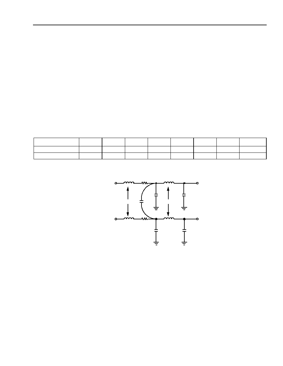
Agere Systems Inc.
67
Data Sheet
October 2001
10 Gbits/s, and 12.5 Gbits/s Line Interface FPSC
ORCA ORLI10G Quad 2.5 Gbits/s
Package Parasitics
The electrical performance of an IC package, such as signal quality and noise sensitivity, is directly affected by the
package parasitics. Table 23 lists eight parasitics associated with the ORCA packages. These parasitics represent
the contributions of all components of a package, which include the bond wires, all internal package routing, and
the external leads.
Four inductances in nH are listed: L
SW
and L
SL,
the self-inductance of the lead; and L
MW
and L
ML
, the mutual
inductance to the nearest neighbor lead. These parameters are important in determining ground bounce noise and
inductive crosstalk noise. Three capacitances in pF are listed: C
M
, the mutual capacitance of the lead to the near-
est neighbor lead; and C
1
and C
2
, the total capacitance of the lead to all other leads (all other leads are assumed
to be grounded). These parameters are important in determining capacitive crosstalk and the capacitive loading
effect of the lead. Resistance values are in m
.
The parasitic values in
Table 23 are for the circuit model of bond wire and package lead parasitics. If the mutual
capacitance value is not used in the designer's model, then the value listed as mutual capacitance should be
added to each of the C
1
and C
2
capacitors.
Table 23. ORCA ORLI10G Package Parasitics
5-3862(C)r2
Figure 26. Package Parasitics
Package Type
L
SW
L
MW
R
W
C
1
C
2
C
M
L
SL
L
ML
416-Pin PBGAM
3.52
0.80
235
0.40
1.0
0.25
1.5--5.0
0.5--1.30
680-Pin PBGAM
3.80
1.30
250
0.50
1.0
0.30
2.8--5.0
0.5--1.50
PAD N
L
SW
R
W
CIRCUIT
BOARD PAD
C
M
C
1
L
SW
R
W
L
SL
L
MW
C
2
C
1
L
ML
C
2
L
SL
PAD N + 1

68
Agere Systems Inc.
Data Sheet
October 2001
10 Gbits/s, and 12.5 Gbits/s Line Interface FPSC
ORCA ORLI10G Quad 2.5 Gbits/s
Package Outline Diagrams
Terms and Definitions
Basic Size (BSC): The basic size of a dimension is the size from which the limits for that dimension are derived by
the application of the allowance and the tolerance.
Design Size: The design size of a dimension is the actual size of the design, including an allowance for fit and tol-
erance.
Typical (TYP): When specified after a dimension, this indicates the repeated design size if a tolerance is specified
or repeated basic size if a tolerance is not specified.
Reference (REF): The reference dimension is an untoleranced dimension used for informational purposes only. It
is a repeated dimension or one that can be derived from other values in the drawing.
Minimum (MIN) or Maximum (MAX): Indicates the minimum or maximum allowable size of a dimension.
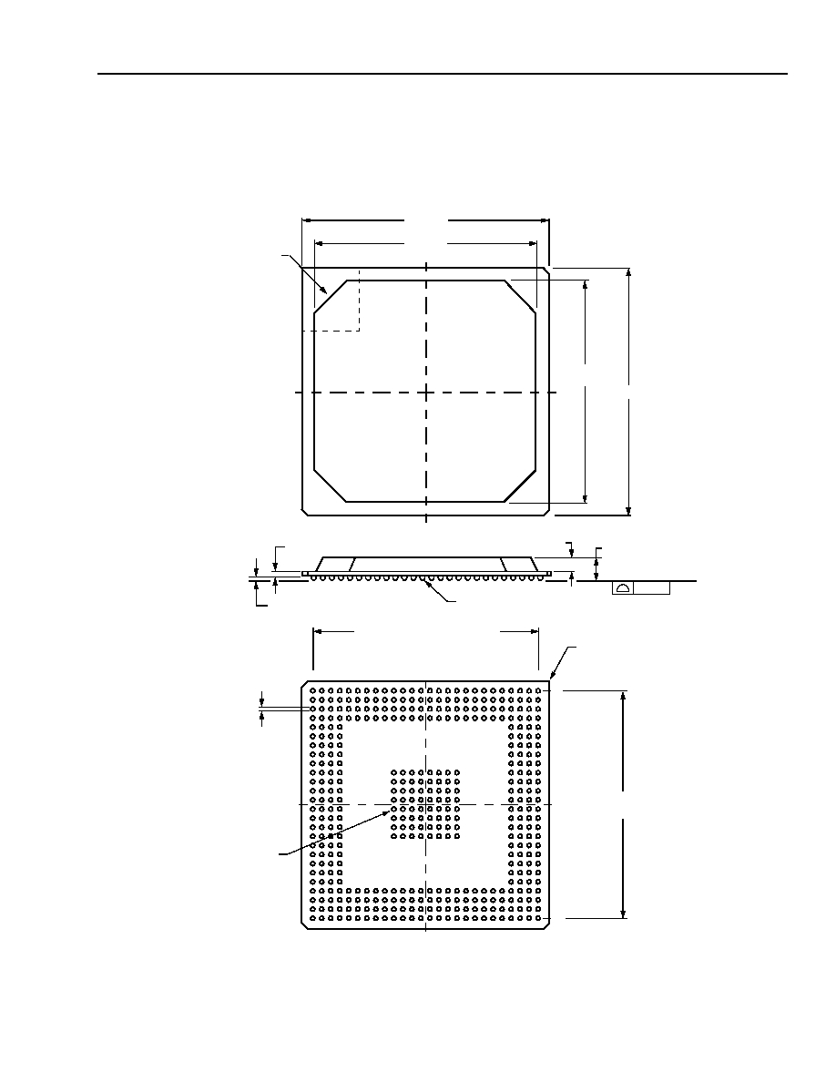
Agere Systems Inc.
69
Data Sheet
October 2001
10 Gbits/s, and 12.5 Gbits/s Line Interface FPSC
ORCA ORLI10G Quad 2.5 Gbits/s
Package Outline Diagrams
(continued)
416-Pin PBGAM
Dimensions are in millimeters.
1139(F)
0.61
±
0.08
1.17
±
0.05
2.28
±
0.10
SEATING PLANE
SOLDER BALL
0.50
±
0.10
0.20
27.00
27.00
24.00
24.00
PIN A1
CORNER
AF
AE
AD
AC
AB
AA
Y
W
V
U
T
R
G
25 SPACES @ 1.00 = 25.00
P
N
M
L
K
J
H
1
2
3
4
5
6
7
8
9
10
12
14
16
18
22
24
26
20
11
13
15
17
21
19
23
25
F
E
D
C
B
A
CENTER ARRAY
FOR THERMAL
ENHANCEMENT
25 SPACES
@ 1.00 = 25.00
A1 BALL
CORNER
0.63
±
0.15
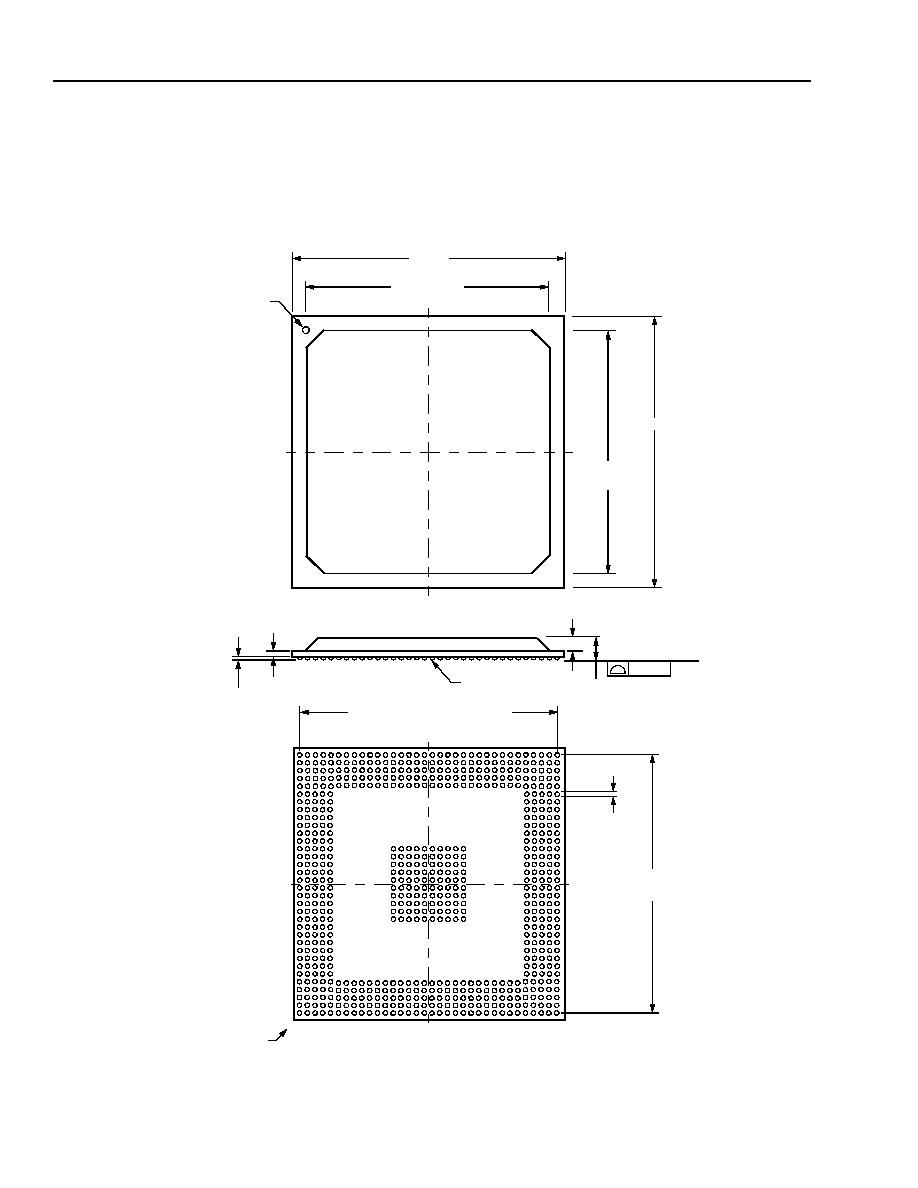
70
Agere Systems Inc.
Data Sheet
October 2001
10 Gbits/s, and 12.5 Gbits/s Line Interface FPSC
ORCA ORLI10G Quad 2.5 Gbits/s
Package Outline Diagrams
(continued)
680-Pin PBGAM
Dimensions are in millimeters.
5-4406(F)
SEATING PLANE
SOLDER BALL
0.50 ± 0.10
0.20
35.00
T
D
H
AL
F
K
B
P
M
L
J
AH
R
C
E
Y
N
U
AN
G
AD
V
AM
AJ
AG
AE
AC
AA
W
AP
AK
AF
AB
A
19
30
26
28
24
32
22
20
18
4
6
8
10
12
14
16
2
34
5
23
25
7
31
29
15
21
3
27
11
17
9
13
1
33
33 SPACES @ 1.00 = 33.00
33 SPACES
A1 BALL
0.64 ± 0.15
A1 BALL
@ 1.00 = 33.00
CORNER
30.00
1.170
+ 0.70
≠ 0.00
35.00
30.00
+ 0.70
≠ 0.00
IDENTIFIER ZONE
2.51 MAX
0.61 ± 0.08
Agere Systems Inc.
71
Data Sheet
October 2001
10 Gbits/s, and 12.5 Gbits/s Line Interface FPSC
ORCA ORLI10G Quad 2.5 Gbits/s
Hardware Ordering Information
5-6435 (F).Q
ORLI10G, ≠1 speed grade, 680-pin plastic ball grid array multilayer (PBGAM).
Table 24. Device Type Options
Table 25. Temperature Options
Table 26. Package Options
Table 27. Package Matrix (Speed Grade)
Software Ordering Information
Implementing a design in an ORLI10G FPSC requires the ORCA Foundry development system and an ORLI10G
design kit. For ordering information please visit:
http://www.agere.com/micro/netcom/ipkits
Device
Voltage
ORLI10G
1.5 V internal
Symbol
Description
Temperature
(Blank)
Industrial
≠40 ∞C to +85 ∞C
Symbol
Description
BM
Plastic Ball Grid Array, Multilayer (PBGAM)
Devices
416-Pin
PBGAM
680-Pin
PBGAM
ORLI10G
≠1, ≠2, ≠3
≠1, ≠2, ≠3
DEVICE TYPE
PACKAGE TYPE
ORLI10G -1 BM
NUMBER OF PINS
680
SPEED GRADE
TEMPERATURE RANGE

Copyright © 2001 Agere Systems Inc.
All Rights Reserved
October 2001
DS01-277NCIP (Replaces DS01-269NCIP)
Agere Systems Inc. reserves the right to make changes to the product(s) or information contained herein without notice. No liability is assumed as a result of their use or application. ORCA is
a registered trademark of Agere Systems Inc. Foundry is a trademark of Xilinx.
For additional information, contact your Agere Systems Account Manager or the following:
INTERNET:
http://www.agere.com or for FPGAs/FPSCs http://www.agere.com/orca
E-MAIL:
docmaster@agere.com
N. AMERICA:
Agere Systems Inc., 555 Union Boulevard, Room 30L-15P-BA, Allentown, PA 18109-3286
1-800-372-2447, FAX 610-712-4106 (In CANADA: 1-800-553-2448, FAX 610-712-4106)
ASIA:
Agere Systems Hong Kong Ltd., Suites 3201 & 3210-12, 32/F, Tower 2, The Gateway, Harbour City, Kowloon
Tel. (852) 3129-2000, FAX (852) 3129-2020
CHINA: (86) 21-5047-1212 (Shanghai), (86) 10-6522-5566 (Beijing), (86) 755-695-7224 (Shenzhen)
JAPAN: (81) 3-5421-1600 (Tokyo), KOREA: (82) 2-767-1850 (Seoul), SINGAPORE: (65) 778-8833, TAIWAN: (886) 2-2725-5858 (Taipei)
EUROPE:
Tel. (44) 7000 624624, FAX (44) 1344 488 045
IEEE is a registered trademark of The Institute of Electrical and Electronics Engineers, Inc.
EIA is a registered trademark of Electronic Industries Association.
PAL is a trademark of Advanced Micro Devices, Inc.
PowerPC is a registered trademark of International Business Machines, Inc.
AMBA is a trademark and ARM is a registered trademark of Advanced RISC Machines Limited.
Synopsys Smart Model is a registered trademark of Synopsys, Inc.
Motorola is a registered trademark of Motorola, Inc.