 | –≠–ª–µ–∫—Ç—Ä–æ–Ω–Ω—ã–π –∫–æ–º–ø–æ–Ω–µ–Ω—Ç: ORT82G5 | –°–∫–∞—á–∞—Ç—å:  PDF PDF  ZIP ZIP |

Preliminary Data Sheet
July 2001
ORCA
Æ
ORT82G5 1.0--1.25/2.0--2.5/3.125 Gbits/s
Backplane Interface FPSC
Introduction
Agere Systems Inc. has developed a next generation
FPSC intended for high-speed serial backplane data
transmission. Built on the Series 4 reconfigurable
embedded system-on-chips (SoC) architecture, the
ORT82G5 is made up of backplane transceivers con-
taining eight channels, each operating at up to
3.125 Gbits/s (2.5 Gbits/s data rate), with a full-
duplex synchronous interface with built-in clock and
data recovery (CDR), along with up to 400k usable
FPGA system gates. The CDR circuitry is a macro-
cell available from Agere's smart silicon macro
library, and has already been implemented in numer-
ous applications including ASICs, standard products,
and FPSCs to create interfaces for SONET/SDH,
STS-48/STM-16, STS-192/STM-64, and 10 Gbit
Ethernet applications. With the addition of protocol
and access logic such as protocol-independent fram-
ers, asynchronous transfer mode (ATM) framers,
packet-over-SONET (POS) interfaces, and framers
for HDLC for Internet protocol (IP), designers can
build a configurable interface retaining proven back-
plane driver/receiver technology. Designers can also
use the device to drive high-speed data transfer
across buses within a system that are not SONET/
SDH based. For example, designers can build a 20
Gbits/s bridge for 10 Gbits/s Ethernet; the high-
speed SERDES interfaces can comprise two XAUI
interfaces with configurable back-end interfaces such
as XGMII or POS-PHY4. The ORT82G5 can also be
used to provide a full 10 Gbits/s backplane data con-
nection with protection between a line card and
switch fabric.
The ORT82G5 offers a clockless high-speed inter-
face for interdevice communication on a board or
across a backplane. The built-in clock recovery of the
ORT82G5 allows for higher system performance,
easier-to-design clock domains in a multiboard sys-
tem, and fewer signals on the backplane. Network
designers will benefit from the backplane transceiver
as a network termination device.The first version of
the device supports 8b/10b encoding/decoding and
link state machines for Ethernet, fibre-channel, and
InfiniBandTM. Version II adds SONET data scram-
bling/descrambling, streamlined SONET framing,
transport overhead handling, plus the programmable
logic to terminate the network into proprietary sys-
tems. For non-SONET applications, all SONET func-
tionality is hidden from the user and no prior
networking knowledge is required.
Version II adds decimation and interpolation for con-
nections at 622 Mbits/s rates.
Table 1. ORCA ORT82G5 Family--Available FPGA Logic
The embedded core and interface are not included in the above gate counts. The usable gate counts range from a logic-only gate count
to a gate count assuming that 20% of the PFUs/SLICs are being used as RAMs. The logic-only gate count includes each PFU/SLIC
(counted as 108 gates/PFU), including 12 gates per LUT/FF pair (eight per PFU), and 12 gates per SLIC/FF pair (one per PFU). Each of
the four PIO groups are counted as 16 gates (three FFs, fast-capture latch, output logic, CLK, and I/O buffers). PFUs used as RAM are
counted at four gates per bit, with each PFU capable of implementing a 32 x 4 RAM (or 512 gates) per PFU. Embedded block RAM
(EBR) is counted as four gates per bit plus each block has an additional 25k gates. 7k gates are used for each PLL and 50k gates for the
embedded system bus and microprocessor interface logic. Both the EBR and PLLs are conservatively utilized in the gate count calcula-
tions.
372 user I/Os out of a total of 432 user I/Os are bonded in the 680 PBGAM package.
Device
PFU
Rows
PFU
Columns
Total
PFUs
User I/O
LUTs
EBR
Blocks
EBR Bits
(k)
Usable
Gates (k)
ORT82G5
36
36
1296
372/432
10,368
12
111
380--800

Table of Contents
Contents
Page
Contents
Page
2
Agere Systems Inc.
Preliminary Data Sheet
July 2001
1.0-1.25/2.0-2.5/3.125 Gbits/s Backplane Interface
ORCA ORT82G5 FPSC Eight-Channel
Introduction..................................................................1
Embedded Function Features .....................................4
Intellectual Property Features......................................4
Programmable Features..............................................5
Programmable Logic System Features .......................6
Description...................................................................7
What Is an FPSC? ....................................................7
FPSC Overview .........................................................7
FPSC Gate Counting ................................................7
FPGA/Embedded Core Interface ..............................7
ORCA Foundry 2000 Development System .............7
FPSC Design Kit .......................................................8
FPGA Logic Overview ...............................................8
PLC Logic ..................................................................8
Programmable I/O .....................................................9
Routing ......................................................................9
System-Level Features..............................................10
Microprocessor Interface .........................................10
System Bus .............................................................10
Phase-Locked Loops ..............................................10
Embedded Block RAM ............................................10
Configuration ...........................................................11
Additional Information .............................................11
ORT82G5 Overview ..................................................11
Device Layout .........................................................11
Backplane Transceiver Interface .............................11
ORT82G5 Overview (continued) ...............................12
Serializer and Deserializer (SERDES) ....................14
MUX/DeMUX Block .................................................14
Multichannel Alignment FIFOs ................................14
XAUI or Fibre-Channel Link State Machine ............14
Dual Port RAMs ......................................................14
FPGA Interface .......................................................15
FPSC Configuration ................................................15
Backplane Transceiver Core Detailed Description ....15
SERDES .................................................................15
SERDES Transmit Path (FPGA ∆ Backplane) ......18
Transmit Preemphasis and Amplitude Control ........19
SERDES Receive Path (Backplane ∆ FPGA) .......19
8b/10b Encoding/Decoding .....................................21
SERDES Transmit and Receive PLLs ................... 21
Reference Clock ..................................................... 21
Byte Alignment ....................................................... 22
Link State Machines ............................................... 22
XAUI Link Synchronization Function ...................... 23
MUX/DeMUX Block ................................................ 25
Multichannel Alignment (Backplane ∆ FPGA) ....... 27
Alignment Sequence .............................................. 29
Loopback Modes .................................................... 32
High-Speed Serial Loopback .................................. 32
Parallel Loopback at the SERDES Boundary ......... 33
Parallel Loopback at MUX/DeMUX Boundary
Excluding SERDES ............................................... 33
ASB Memory Blocks ............................................... 34
Memory Map............................................................. 36
Definition of Register Types ................................... 36
Absolute Maximum Ratings...................................... 54
Recommended Operating Conditions ...................... 54
HSI Electrical and Timing Characteristics ................ 54
Pin Information ......................................................... 57
Power Supplies for ORT82G5 ................................ 63
Recommended Power Supply Connections ........... 64
Recommended Power Supply Filtering Scheme .... 64
Package Pinouts .................................................... 69
Pin Information ......................................................... 70
Package Thermal Characteristics
Summary.................................................................. 87
JA ......................................................................... 87
JC ........................................................................ 87
JC ........................................................................ 87
JB ........................................................................ 87
FPSC Maximum Junction Temperature ................. 87
Package Thermal Characteristics............................. 88
Package Coplanarity ................................................ 88
Package Parasitics ................................................... 88
Package Outline Diagrams....................................... 89
Terms and Definitions ............................................ 89
680-Pin PBGAM ..................................................... 90
Hardware Ordering Information ................................ 91
Software Ordering Information ................................. 91

Agere Systems Inc.
3
Preliminary Data Sheet
July 2001
1.0-1.25/2.0-2.5/3.125 Gbits/s Backplane Interface
ORCA ORT82G5 FPSC Eight-Channel
Table of Contents
List of Figures
Page
List of Tables
Page
Figure 1. ORT82G5 Block Diagram ..........................12
Figure 2. Internal High-Level Diagram of ORT82G5
Transceiver ..............................................................13
Figure 3. SERDES Functional Block Diagram for
One Channel ...........................................................17
Figure 4. ORT82G5 Transmit Path for a Single
SERDES Channel ...................................................18
Figure 5. ORT82G5 Receive Path for a Single
SERDES Channel ...................................................20
Figure 6. Fibre-Channel Link State Machine State
Diagram ...................................................................22
Figure 7. XAUI Link Synchronization State
Diagram ...................................................................24
Figure 8. Transmit MUX Block for a Single SERDES
Channel ...................................................................25
Figure 9. Receive DeMUX Block for a Single
SERDES Channel ...................................................26
Figure 10. Interconnect of Streams for FIFO ............27
Figure 11. Example of SERDES A Alignment and ...27
Figure 12. Example of SERDES A and B
Alignment ................................................................27
Figure 13. Example of Multiple Twin Channel ..........27
Figure 14. Multichannel Alignment FIFO Block for
a Single SERDES Channel .....................................28
Figure 15. De-Skew Lanes by Aligning /A/
Columns ..................................................................30
Figure 16. Block Diagram of Memory Block .............34
Figure 17. Minimum Timing Specs for Memory
Blocks-Write Cycle ..................................................35
Figure 18. Minimum Timing Specs for Memory
Blocks-Read Cycle ..................................................35
Figure 19. Receive Data Eye-diagram Template
(Differential) .............................................................55
Figure 20. Power Supply Filtering ............................65
Figure 21. Package Parasitics ..................................88
Table 1. ORCA ORT82G5 Family--Available
FPGA Logic ...............................................................1
Table 2. Preemphasis Settings ...................................19
Table 3. Transmit PLL Clock and Data Rates ............21
Table 4. Receive PLL Clock and Data Rates .............21
Table 5. XAUI Link Synchronization State
Diagram Notation--Variables ..................................23
Table 6. XAUI Link Synchronization State
Diagram--Functions ................................................23
Table 7. Multichannel Alignment Modes .....................29
Table 8. Definition of Bits of MRWDxy[39:0] ...............31
Table 9. High-Speed Serial Loopback Configuration .32
Table 10. Parallel Loopback Configuration .................33
Table 11. Structural Register Elements ......................36
Table 12. Memory Map ...............................................37
Table 13. Absolute Maximum Ratings ........................54
Table 14. Recommended Operating Conditions ........54
Table 15. Absolute Maximum Ratings ........................54
Table 16. Recommended Operating Conditions ........54
Table 17. Receiver Specifications ..............................55
Table 18. Reference Clock Specifications
(REFINP and REFINN) ............................................56
Table 19. Channel Output Jitter (1.25 Gbits/s) ...........56
Table 20. Channel Output Jitter (2.5 Gbits/s) .............56
Table 21. Serial Output Timing Levels (CML I/O) .......56
Table 22. Serial Input Timing and Levels (CML I/O) ...56
Table 23. FPGA Common-Function Pin Description ..57
Table 24. FPSC Function Pin Description ..................60
Table 25. Power Supply Pin Groupings ......................63
Table 26. Embedded Core/FPGA Interface
Signal Description ...................................................66
Table 27. ORT82G5 680-Pin PBGAM Pinout .............70
Table 28. ORCA ORT82G5 Plastic Package
Thermal Guidelines .................................................88
Table 29. ORCA ORT82G5 Package Parasitics ........88
Table 30. Device Type Options ..................................91
Table 31. Temperature Options ..................................91
Table 32. Package Type Options ...............................91
Table 33. ORCA FPSC Package Matrix
(Speed Grades) .......................................................91

4
4
Agere Systems Inc.
Preliminary Data Sheet
July 2001
1.0-1.25/2.0-2.5/3.125 Gbits/s Backplane Interface
ORCA ORT82G5 FPSC Eight-Channel
Embedded Function Features
s
High-speed SERDES programmable serial data
rates of 622 Mbits/s (SONET only), 1.25 Gbits/s,
2.5 Gbits/s, and 3.125 Gbits/s.
s
Asynchronous operation per receive channel with the
receiver frequency tolerance based on one reference
clock per quad channels (separate PLL per channel).
s
Ability to select full-rate or half-rate operation per Tx
or Rx channel by setting the appropriate control reg-
isters.
s
Transmit preemphasis (programmable) for improved
receive data eye opening.
s
Receiver energy detector to determine if a link is
active.
s
32-bit (SONET or 8b/10b) or 40-bit (raw data) paral-
lel internal bus for data processing in FPGA logic.
s
Provides a 10 Gbits/s backplane interface to switch
fabric with protection. Also supports port cards at
622 Mbits/s or 2.5 Gbits/s.
s
3.125 Gbits/s SERDES compliant with XAUI serial
data specification for 10 Gbit Ethernet applications
with protection.
s
Most XAUI features for 10 Gbit Ethernet are embed-
ded including the required link state machine.
s
Compliant to fibre-channel physical layer specifica-
tion.
s
Allows wide range of applications for SONET net-
work termination, as well as generic data moving for
high-speed backplane data transfer.
s
No knowledge of SONET/SDH needed in generic
applications. Simply supply data, a 100 MHz--
156.25 MHz reference clock, and, optionally, a frame
pulse.
s
High-speed interface (HSI) function for clock/data
recovery serial backplane data transfer without exter-
nal clocks.
s
Eight-channel HSI function provides 2.5 Gbits/s
serial user data interface per channel for a total chip
bandwidth of 20 Gbits/s (full duplex).
s
SERDES has low-power CML buffers. Support for
1.5 V/1.8 V I/Os.
s
Programmable STS-12 or STS-48 framing in SONET
mode per channel (in version II). OC-192 framing in
quad OC-48 (four channels) also supported.
s
Powerdown option of SERDES HSI receiver on a
per-channel basis.
s
Selectable 8b/10b coder/decoder or SONET scram-
bler/descrambler (added for version 2).
s
SERDES HSI automatically recovers from loss-of-
clock once its reference clock returns to normal oper-
ating state.
s
In-band management and configuration through
transport overhead extraction/insertion in SONET
mode (version II).
s
Supports transparent mode where the only insertion
is A1/A2 framing bytes in SONET mode (version II).
s
Built-in boundary scan (IEEE
Æ
1149.1 and 1149.2
JTAG) for the programmable I/Os, not including the
SERDES interface.
s
FIFOs align incoming data across all eight channels
(all eight channels, two groups of four channels, or
four groups of two channels). Alignment is done
using comma characters or /A/ in 8b/10b mode or
frame pulse in SONET mode (version II). Optional
ability to bypass alignment FIFOs for asynchronous
operation between channels. (Each channel includes
its own clock and frame pulse or comma detect.)
s
Frame alignment across multiple ORT82G5 devices
for work/protect switching at STS-768/STM256 and
above rates in SONET mode.
s
Addition of two 4K X 36 dual-port RAMs with access
to the programmable logic.
Intellectual Property Features
Programmable logic provides a variety of yet-to-be
standardized interface functions, including the following
Agere ME IP core functions:
s
10 Gbits/s Ethernet as defined by IEEE 802.3ae:
-- XGMII for interfacing to 10 Gbits/s Ethernet
MACs. XGMII is a 156 MHz double data rate par-
allel short reach (typically less than 2") intercon-
nect interface.
-- X
58
+ X
39
+ X
1
scrambler/descrambler for
10 Gbits/s Ethernet.
-- 64b/66b encoders/decoders for 10 Gbits/s Ether-
net.
-- XAUI to XGMII translator, including dual XAUI pro-
tection.
s
POS-PHY4 interface for 10 Gbits/s SONET/SDH and
OTN systems and some 10 Gbits/s Ethernet systems
to allow easy integration of InfiniBand, fibre-channel,
and 10 Gbits/s Ethernet in data over fibre applica-
tions.
s
Ethernet MAC functions at 10/100 Mbits/s, 1 Gbits/s,
and 10 Gbits/s.
s
Other functions such as fibre-channel and InfiniBand
link layer IP cores are also going to be developed.

Agere Systems Inc.
5
Preliminary Data Sheet
July 2001
1.0-1.25/2.0-2.5/3.125 Gbits/s Backplane Interface
ORCA ORT82G5 FPSC Eight-Channel
Programmable Features
s
High-performance programmable logic:
-- 0.13 µm 7-level metal technology.
-- Internal performance of >250 MHz.
-- Over 400k usable system gates.
-- Meets multiple I/O interface standards.
-- 1.5 V operation (30% less power than 1.8 V oper-
ation) translates to greater performance.
s
Traditional I/O selections:
-- LVTTL and LVCMOS (3.3 V, 2.5 V, and 1.8 V) I/Os.
-- Per pin-selectable I/O clamping diodes provide
3.3 V PCI compliance.
-- Individually programmable drive capability:
24 mA sink/12 mA source, 12 mA sink/6 mA
source, or 6 mA sink/3 mA source.
-- Two slew rates supported (fast and slew-limited).
-- Fast-capture input latch and input flip-flop
(FF)/latch for reduced input setup time and zero
hold time.
-- Fast open-drain drive capability.
-- Capability to register 3-state enable signal.
-- Off-chip clock drive capability.
-- Two-input function generator in output path.
s
New programmable high-speed I/O:
-- Single-ended: GTL, GTL+, PECL, SSTL3/2
(class I and II), HSTL (Class I, III, IV), ZBT, and
DDR.
-- Double-ended: LVDS, bused-LVDS, and LVPECL.
Programmable, parallel termination (100
) is
also supported for these I/Os.
-- Customer defined: ability to substitute arbitrary
standard cell I/O to meet fast-moving standards.
s
New capability to (de)multiplex I/O signals:
-- New DDR on both input and output at rates up to
311 MHz (622 MHz effective rate).
-- New 2x and 4x downlink and uplink capability per
I/O (i.e., 50 MHz internal to 200 MHz I/O).
s
Enhanced twin-quad programmable function unit
(PFU):
-- Eight 16-bit look-up tables (LUTs) per PFU.
-- Nine user registers per PFU, one following each
LUT, and organized to allow two nibbles to act
independently, plus one extra for arithmetic opera-
tions.
-- New register control in each PFU has two inde-
pendent programmable clocks, clock enables,
local set/reset, and data selects.
-- New LUT structure allows flexible combinations of
LUT4, LUT5, new LUT6, 4
1 MUX, new
8
1 MUX, and ripple mode arithmetic functions
in the same PFU.
-- 32 x 4 RAM per PFU, configurable as single- or
dual-port. Create large, fast RAM/ROM blocks
(128 x 8 in only eight PFUs) using the SLIC
decoders as bank drivers.
-- Soft-wired LUTs (SWL) allow fast cascading of up
to three levels of LUT logic in a single PFU
through fast internal routing which reduces rout-
ing congestion and improves speed.
-- Flexible fast access to PFU inputs from routing.
-- Fast-carry logic and routing to all four adjacent
PFUs for nibble-wide, byte-wide, or longer arith-
metic functions, with the option to register the
PFU carry-out.
s
Abundant high-speed buffered and nonbuffered rout-
ing resources provide 2x average speed improve-
ments over previous architectures.
s
Hierarchical routing optimized for both local and glo-
bal routing with dedicated routing resources. This
results in faster routing times with predictable and
efficient performance.
s
SLIC provides eight 3-statable buffers, up to a 10-bit
decoder, and PALTM-like and-or-invert (AOI) in each
programmable logic cell.
s
New 200 MHz embedded quad-port RAM blocks,
2 read ports, 2 write ports, and 2 sets of byte lane
enables. Each embedded RAM block can be config-
ured as:
-- 1--512 x 18 (quad-port, two read/two write) with
optional built in arbitration.
-- 1--256 x 36 (dual-port, one read/one write).
-- 1--1k x 9 (dual-port, one read/one write).
-- 2--512 x 9 (dual-port, one read/one write for
each).
-- 2 RAMS with arbitrary number of words whose
sum is 512 or less by 18 (dual-port, one read/one
write).
-- Supports joining of RAM blocks.
-- Two 16 x 8-bit content addressable memory
(CAM) support.
-- FIFO 512 x 18, 256 x 36, 1k x 9, or dual 512 x 9.
-- Constant multiply (8 x 16 or 16 x 8).
-- Dual variable multiply (8 x 8).
s
Embedded 32-bit internal system bus plus 4-bit par-
ity interconnects FPGA logic, microprocessor inter-
face (MPI), embedded RAM blocks, and embedded
standard cell blocks with 66 MHz bus performance.
Included are built-in system registers that act as the
control and status center for the device.

6
6
Agere Systems Inc.
Preliminary Data Sheet
July 2001
1.0-1.25/2.0-2.5/3.125 Gbits/s Backplane Interface
ORCA ORT82G5 FPSC Eight-Channel
Programmable Features
(continued)
s
Built-in testability:
-- Full boundary scan (IEEE 1149.1 and Draft
1149.2 JTAG).
-- Programming and readback through boundary
scan port compliant to IEEE Draft 1532:D1.7.
-- TS_ALL testability function to 3-state all I/O pins.
-- New temperature-sensing diode.
s
Improved built-in clock management with program-
mable phase-locked loops (PPLLs) provide optimum
clock modification and conditioning for phase, fre-
quency, and duty cycle from 20 MHz up to 420 MHz.
s
New cycle stealing capability allows a typical 15% to
40% internal speed improvement after final place
and route. This feature also enables compliance with
many setup/hold and clock to out I/O specifications
and may provide reduced ground bounce for output
buses by allowing flexible delays of switching output
buffers.
Programmable Logic System Features
s
PCI local bus compliant for FPGA I/Os.
s
Improved PowerPC
Æ
860 and PowerPC II high-
speed synchronous microprocessor interface can be
used for configuration, readback, device control, and
device status, as well as for a general-purpose inter-
face to the FPGA logic, RAMs, and embedded stan-
dard cell blocks. Glueless interface to synchronous
PowerPC processors with user-configurable address
space provided.
s
New embedded AMBA
TM
specification 2.0 AHB sys-
tem bus (ARM
Æ
processor) facilitates communica-
tion among the microprocessor interface,
configuration logic, embedded block RAM, FPGA
logic, and embedded standard cell blocks.
s
New network PLLs meet ITU-T G.811 specifications
and provide clock conditioning for DS-1/E-1 and
STS-3/STM-1 applications.
s
Flexible general purpose PPLLs offer clock multiply
(up to 8x), divide (down to 1/8x), phase shift, delay
compensation, and duty cycle adjustment combined.
s
Variable size bused readback of configuration data
capability with the built-in microprocessor interface
and system bus.
s
Internal, 3-state, and bidirectional buses with simple
control provided by the SLIC.
s
New clock routing structures for global and local
clocking significantly increases speed and reduces
skew (<200 ps for OR4E4).
s
New local clock routing structures allow creation of
localized clock trees.
s
New double-data rate (DDR) and zero-bus turn-
around (ZBT) memory interfaces support the latest
high-speed memory interfaces.
s
New 2x/4x uplink and downlink I/O capabilities inter-
face high-speed external I/Os to reduced speed
internal logic.
s
ORCA Foundry 2000 development system software.
Supported by industry-standard CAE tools for design
entry, synthesis, simulation, and timing analysis.
s
Meets universal test and operations PHY interface
for ATM (UTOPIA) Levels 1, 2, and 3; as well as
POS-PHY3. Also meets proposed specifications for
UTOPIA Level 4 and POS-PHY3 (2.5 Gbits/s) and
POS-PHY4 (10 Gbits/s) interface standards for
packet-over-SONET as defined by the Saturn Group.
s
Two new edge clock routing structures allow up to
seven high-speed clocks on each edge of the device
for improved setup/hold and clock to out perfor-
mance.

Agere Systems Inc.
7
Preliminary Data Sheet
July 2001
1.0-1.25/2.0-2.5/3.125 Gbits/s Backplane Interface
ORCA ORT82G5 FPSC Eight-Channel
Description
What Is an FPSC?
FPSCs, or field-programmable system chips, are
devices that combine field-programmable logic with
ASIC or mask-programmed logic on a single device.
FPSCs provide the time to market and the flexibility of
FPGAs, the design effort savings of using soft intellec-
tual property (IP) cores, and the speed, design density,
and economy of ASICs.
FPSC Overview
Agere's Series 4 FPSCs are created from Series 4
ORCA FPGAs. To create a Series 4 FPSC, several col-
umns of programmable logic cells (see FPGA Logic
Overview section for FPGA logic details) are added to
an embedded logic core. Other than replacing some
FPGA gates with ASIC gates, at greater than 10:1 effi-
ciency, none of the FPGA functionality is changed--all
of the Series 4 FPGA capability is retained: embedded
block RAMs, MPI, PCMs, boundary scan, etc. The col-
umns of programmable logic are replaced at the right of
the device, allowing pins from the replaced columns to
be used as I/O pins for the embedded core. The
remainder of the device pins retain their FPGA func-
tionality.
The embedded cores can take many forms and gener-
ally come from Agere's ASIC libraries. Other offerings
allow customers to supply their own core functions for
the creation of custom FPSCs.
FPSC Gate Counting
The total gate count for an FPSC is the sum of its
embedded core (standard-cell/ASIC gates) and its
FPGA gates. Because FPGA gates are generally
expressed as a usable range with a nominal value, the
total FPSC gate count is sometimes expressed in the
same manner. Standard-cell ASIC gates are, however,
10 to 25 times more silicon-area efficient than FPGA
gates. Therefore, an FPSC with an embedded function
is gate equivalent to an FPGA with a much larger gate
count.
FPGA/Embedded Core Interface
The interface between the FPGA logic and the embed-
ded core has been enhanced to allow for a greater
number of interface signals than on previous FPSC
architectures. Compared to bringing embedded core
signals off-chip, this on-chip interface is much faster
and requires less power. All of the delays for the inter-
face are precharacterized and accounted for in the
ORCA Foundry Development System.
Series 4 based FPSCs expand this interface by provid-
ing a link between the embedded block and the multi-
master 32-bit system bus in the FPGA logic. This sys-
tem bus allows the core easy access to many of the
FPGA logic functions including the embedded block
RAMs and the microprocessor interface.
Clock spines also can pass across the FPGA/embed-
ded core boundary. This allows for fast, low-skew clock-
ing between the FPGA and the embedded core. Many
of the special signals from the FPGA, such as DONE
and global set/reset, are also available to the embed-
ded core, making it possible to fully integrate the
embedded core with the FPGA as a system.
For even greater system flexibility, FPGA configuration
RAMs are available for use by the embedded core. This
allows for user-programmable options in the embedded
core, in turn allowing for greater flexibility. Multiple
embedded core configurations may be designed into a
single device with user-programmable control over
which configurations are implemented, as well as the
capability to change core functionality simply by recon-
figuring the device.
ORCA
Foundry
2000 Development System
The ORCA Foundry 2000 development system is used
to process a design from a netlist to a configured
FPGA. This system is used to map a design onto the
ORCA architecture, and then place and route it using
ORCA Foundry's timing-driven tools. The development
system also includes interfaces to, and libraries for,
other popular CAE tools for design entry, synthesis,
simulation, and timing analysis.
The ORCA Foundry 2000 development system inter-
faces to front-end design entry tools and provides the
tools to produce a configured FPGA. In the design flow,
the user defines the functionality of the FPGA at two
points in the design flow: design entry and the bit-
stream generation stage. Recent improvements in
ORCA Foundry allow the user to provide timing
requirement information through logical preferences
only; thus, the designer is not required to have physical
knowledge of the implementation.

8
8
Agere Systems Inc.
Preliminary Data Sheet
July 2001
1.0-1.25/2.0-2.5/3.125 Gbits/s Backplane Interface
ORCA ORT82G5 FPSC Eight-Channel
Description
(continued)
Following design entry, the development system's map,
place, and route tools translate the netlist into a routed
FPGA. A floorplanner is available for layout feedback
and control. A static timing analysis tool is provided to
determine device speed and a back-annotated netlist
can be created to allow simulation and timing.
Timing and simulation output files from ORCA Foundry
are also compatible with many third-party analysis
tools. Its bit stream generator is then used to generate
the configuration data which is loaded into the FPGAs
internal configuration RAM, embedded block RAM,
and/or FPSC memory.
When using the bit stream generator, the user selects
options that affect the functionality of the FPGA. Com-
bined with the front-end tools, ORCA Foundry pro-
duces configuration data that implements the various
logic and routing options discussed in this data sheet.
FPSC Design Kit
Development is facilitated by an FPSC design kit
which, together with ORCA Foundry and third-party
synthesis and simulation engines, provides all software
and documentation required to design and verify an
FPSC implementation. Included in the kit are the FPSC
configuration manager, Synopsys Smart Model
Æ
, and
complete online documentation. The kit's software cou-
ples with ORCA Foundry, providing a seamless FPSC
design environment. More information can be obtained
by visiting the ORCA website or contacting a local
sales office, both listed on the last page of this docu-
ment.
FPGA Logic Overview
The ORCA Series 4 architecture is a new generation of
SRAM-based programmable devices from Agere. It
includes enhancements and innovations geared toward
today's high-speed systems on a single chip. Designed
with networking applications in mind, the Series 4 fam-
ily incorporates system-level features that can further
reduce logic requirements and increase system speed.
ORCA Series 4 devices contain many new patented
enhancements and are offered in a variety of packages
and speed grades.
The hierarchical architecture of the logic, clocks, rout-
ing, RAM, and system-level blocks create a seamless
merge of FPGA and ASIC designs. Modular hardware
and software technologies enable system-on-chip inte-
gration with true plug-and-play design implementation.
The architecture consists of four basic elements: pro-
grammable logic cells (PLCs), programmable I/O cells
(PIOs), embedded block RAMs (EBRs), and system-
level features. These elements are interconnected with
a rich routing fabric of both global and local wires. An
array of PLCs are surrounded by common interface
blocks which provide an abundant interface to the adja-
cent PLCs or system blocks. Routing congestion
around these critical blocks is eliminated by the use of
the same routing fabric implemented within the pro-
grammable logic core. Each PLC contains a PFU,
SLIC, local routing resources, and configuration RAM.
Most of the FPGA logic is performed in the PFU, but
decoders, PAL-like functions, and 3-state buffering can
be performed in the SLIC. The PIOs provide device
inputs and outputs and can be used to register signals
and to perform input demultiplexing, output multiplex-
ing, uplink and downlink functions, and other functions
on two output signals. Large blocks of 512 x 18 quad-
port RAM complement the existing distributed PFU
memory. The RAM blocks can be used to implement
RAM, ROM, FIFO, multiplier, and CAM. Some of the
other system-level functions include the MPI, PLLs,
and the embedded system bus (ESB).
PLC Logic
Each PFU within a PLC contains eight 4-input (16-bit)
LUTs, eight latches/FFs, and one additional flip-flop
that may be used independently or with arithmetic func-
tions.
The PFU is organized in a twin-quad fashion; two sets
of four LUTs and FFs that can be controlled indepen-
dently. Each PFU has two independent programmable
clocks, clock enables, local set/reset, and data selects.
LUTs may also be combined for use in arithmetic func-
tions using fast-carry chain logic in either 4-bit or 8-bit
modes. The carry-out of either mode may be registered
in the ninth FF for pipelining. Each PFU may also be
configured as a synchronous 32 x 4 single- or dual-port
RAM or ROM. The FFs (or latches) may obtain input
from LUT outputs or directly from invertible PFU inputs,
or they can be tied high or tied low. The FFs also have
programmable clock polarity, clock enables, and local
set/reset.

Agere Systems Inc.
9
Preliminary Data Sheet
July 2001
1.0-1.25/2.0-2.5/3.125 Gbits/s Backplane Interface
ORCA ORT82G5 FPSC Eight-Channel
Description
(continued)
The SLIC is connected from PLC routing resources
and from the outputs of the PFU. It contains eight
3-state, bidirectional buffers, and logic to perform up to
a 10-bit AND function for decoding, or an AND-OR with
optional INVERT to perform PAL-like functions. The
3-state drivers in the SLIC and their direct connections
from the PFU outputs make fast, true, 3-state buses
possible within the FPGA, reducing required routing
and allowing for real-world system performance.
Programmable I/O
The Series 4 PIO addresses the demand for the flexi-
bility to select I/Os that meet system interface require-
ments. I/Os can be programmed in the same manner
as in previous ORCA devices, with the additional new
features which allow the user the flexibility to select
new I/O types that support high-speed interfaces.
Each PIO contains four programmable I/O pads and is
interfaced through a common interface block to the
FPGA array. The PIO is split into two pairs of I/O pads
with each pair having independent clock enables, local
set/reset, and global set/reset. On the input side, each
PIO contains a programmable latch/flip-flop which
enables very fast latching of data from any pad. The
combination provides for very low setup requirements
and zero hold times for signals coming on-chip. It may
also be used to demultiplex an input signal, such as a
multiplexed address/data signal, and register the sig-
nals without explicitly building a demultiplexer with a
PFU.
On the output side of each PIO, an output from the PLC
array can be routed to each output flip-flop, and logic
can be associated with each I/O pad. The output logic
associated with each pad allows for multiplexing of out-
put signals and other functions of two output signals.
The output FF, in combination with output signal multi-
plexing, is particularly useful for registering address
signals to be multiplexed with data, allowing a full clock
cycle for the data to propagate to the output. The out-
put buffer signal can be inverted, and the 3-state con-
trol can be made active-high, active-low, or always
enabled. In addition, this 3-state signal can be regis-
tered or nonregistered.
The Series 4 I/O logic has been enhanced to include
modes for speed uplink and downlink capabilities.
These modes are supported through shift register
logic, which divides down incoming data rates or multi-
plies up outgoing data rates. This new logic block also
supports high-speed DDR mode requirements where
data is clocked into and out of the I/O buffers on both
edges of the clock.
The new programmable I/O cell allows designers to
select I/Os which meet many new communication stan-
dards permitting the device to hook up directly without
any external interface translation. They support tradi-
tional FPGA standards as well as high-speed, single-
ended, and differential-pair signaling (as shown in
Table 1). Based on a programmable, bank-oriented I/O
ring architecture, designs can be implemented using
3.3 V, 2.5 V, 1.8 V, and 1.5 V referenced output levels.
Routing
The abundant routing resources of the Series 4 archi-
tecture are organized to route signals individually or as
buses with related control signals. Both local and global
signals utilize high-speed buffered and nonbuffered
routes. One PLC segmented (x1), six PLC segmented
(x6), and bused half chip (xHL) routes are patterned
together to provide high connectivity with fast software
routing times and high-speed system performance.
Eight fully distributed primary clocks are routed on a
low-skew, high-speed distribution network and may be
sourced from dedicated I/O pads, PLLs, or the PLC
logic. Secondary and edge-clock routing is available for
fast regional clock or control signal routing for both
internal regions and on device edges. Secondary clock
routing can be sourced from any I/O pin, PLLs, or the
PLC logic.
The improved routing resources offer great flexibility in
moving signals to and from the logic core. This flexibil-
ity translates into an improved capability to route
designs at the required speeds when the I/O signals
have been locked to specific pins.

10
10
Agere Systems Inc.
Preliminary Data Sheet
July 2001
1.0-1.25/2.0-2.5/3.125 Gbits/s Backplane Interface
ORCA ORT82G5 FPSC Eight-Channel
System-Level Features
The Series 4 also provides system-level functionality by
means of its microprocessor interface, embedded sys-
tem bus, quad-port embedded block RAMs, universal
programmable phase-locked loops, and the addition of
highly tuned networking specific phase-locked loops.
These functional blocks allow for easy glueless system
interfacing and the capability to adjust to varying condi-
tions in today's high-speed networking systems.
Microprocessor Interface
The MPI provides a glueless interface between the
FPGA and PowerPC microprocessors. Programmable
in 8-, 16-, and 32-bit interfaces with optional parity to
the Motorola
Æ
PowerPC 860 bus, it can be used for
configuration and readback, as well as for FPGA con-
trol and monitoring of FPGA status. All MPI transac-
tions utilize the Series 4 embedded system bus at 66
MHz performance.
A system-level microprocessor interface to the FPGA
user-defined logic following configuration, through the
system bus, including access to the embedded block
RAM and general user-logic, is provided by the MPI.
The MPI supports burst data read and write transfers,
allowing short, uneven transmission of data through the
interface by including data FIFOs. Transfer accesses
can be single beat (1 x 4 bytes or less), 4-beat (4 x
4 bytes), 8-beat (8 x 2 bytes), or 16-beat (16 x 1 bytes).
System Bus
An on-chip, multimaster, 8-bit system bus with 1-bit
parity facilitates communication among the MPI, config-
uration logic, FPGA control, and status registers,
embedded block RAMs, as well as user logic. Utilizing
the AMBA specification Rev 2.0 AHB protocol, the
embedded system bus offers arbiter, decoder, master,
and slave elements. Master and slave elements are
also available for the user-logic and embedded back-
plane transceiver portion of the ORT82G5.
The system bus control registers can provide control to
the FPGA such as signaling for reprogramming, reset
functions, and PLL programming. Status registers mon-
itor INIT, DONE, and system bus errors. An interrupt
controller is integrated to provide up to eight possible
interrupt resources. Bus clock generation can be
sourced from the microprocessor interface clock, con-
figuration clock (for slave configuration modes), internal
oscillator, user clock from routing, or from the port clock
(for JTAG configuration modes).
Phase-Locked Loops
Up to eight PLLs are provided on each Series 4 device,
with four PLLs generally provided for FPSCs. Program-
mable PLLs can be used to manipulate the frequency,
phase, and duty cycle of a clock signal. Each PPLL is
capable of manipulating and conditioning clocks from
20 MHz to 420 MHz. Frequencies can be adjusted from
1/8x to 8x, the input clock frequency. Each programma-
ble PLL provides two outputs that have different multi-
plication factors but can have the same phase
relationships. Duty cycles and phase delays can be
adjusted in 12.5% of the clock period increments. An
automatic input buffer delay compensation mode is
available for phase delay. Each PPLL provides two out-
puts that can have programmable (12.5% steps) phase
differences.
Additional highly tuned and characterized, dedicated
phase-locked loops (DPLLs) are included to ease sys-
tem designs. These DPLLs meet ITU-T G.811 primary-
clocking specifications and enable system designers to
very tightly target specified clock conditioning not tradi-
tionally available in the universal PPLLs. Initial DPLLs
are targeted to low-speed networking DS1 and E1, and
also high-speed SONET/SDH networking STS-3 and
STM-1 systems. These DPLLs are not typically
included on FPSC devices and are not found on the
ORT82G5.
Embedded Block RAM
New 512 x 18 quad-port RAM blocks are embedded in
the FPGA core to significantly increase the amount of
memory and complement the distributed PFU memo-
ries. The EBRs include two write ports, two read ports,
and two byte lane enables which provide four-port
operation. Optional arbitration between the two write
ports is available, as well as direct connection to the
high-speed system bus.
Additional logic has been incorporated to allow signifi-
cant flexibility for FIFO, constant multiply, and two-vari-
able multiply functions. The user can configure FIFO
blocks with flexible depths of 512k, 256k, and 1k includ-
ing asynchronous and synchronous modes and pro-
grammable status and error flags. Multiplier capabilities
allow a multiple of an 8-bit number with a 16-bit fixed
coefficient or vice versa (24-bit output), or a multiply of
two 8-bit numbers (16-bit output). On-the-fly coefficient
modifications are available through the second read/
write port. Two 16 x 8-bit CAMs per embedded block
can be implemented in single match, multiple match,
and clear modes. The EBRs can also be preloaded at
device configuration time.

Agere Systems Inc.
11
Preliminary Data Sheet
July 2001
1.0-1.25/2.0-2.5/3.125 Gbits/s Backplane Interface
ORCA ORT82G5 FPSC Eight-Channel
System-Level Features
(continued)
Configuration
The FPGAs functionality is determined by internal con-
figuration RAM. The FPGAs internal initialization/con-
figuration circuitry loads the configuration data at
powerup or under system control. The configuration
data can reside externally in an EEPROM or any other
storage media. Serial EEPROMs provide a simple, low
pin-count method for configuring FPGAs.
The RAM is loaded by using one of several configura-
tion modes. Supporting the traditional master/slave
serial, master/slave parallel, and asynchronous periph-
eral modes, the Series 4 also utilizes its microproces-
sor interface and embedded system bus to perform
both programming and readback. Daisy chaining of
multiple devices and partial reconfiguration are also
permitted.
Other configuration options include the initialization of
the embedded-block RAM memories and FPSC mem-
ory as well as system bus options and bit stream error
checking. Programming and readback through the
JTAG (IEEE 1149.2) port is also available meeting in-
system programming (ISP) standards (IEEE 1532
Draft).
Additional Information
Contact your local Agere representative for additional
information regarding the ORCA Series 4 FPGA
devices, or visit our website at:
http://www.agere.com/orca
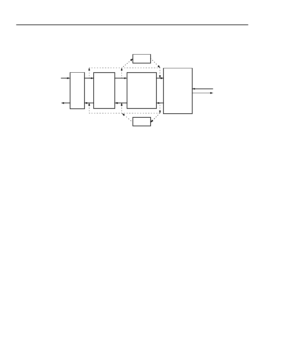
ORT82G5 Overview
Device Layout
The ORT82G5 is a backplane transceiver FPSC with
embedded CDR and SERDES circuitry and 8b/10b
encoding/decoding. It is intended for high-speed serial
backplane data transmission. Built using Series 4
reconfigurable system-on-chips (SoC) architecture, it
also contains up to 400k usable FPGA system gates.
The ORT82G5 contains an FPGA base array, an eight-
channel clock and data recovery macro, and an eight-
channel 8b/10b interface on a single monolithic chip.
version II of this device, which will be plug-in compati-
ble to version I, also adds SONET scrambling capabil-
ity. The version II features are not described in this data
sheet. Figure 1 shows the ORT82G5 block diagram.
Boundary scan for the ORT82G5 only includes pro-
grammable I/Os and does not include any of the
embedded block I/Os.
Backplane Transceiver Interface
The ORT82G5 backplane transceiver FPSC has eight
channels, each operating at up to 3.125 Gbits/s
(2.5 Gbits/s data rate) with a full-duplex synchronous
interface with built-in clock recovery (CDR). The CDR
macro with 8b/10b provides guaranteed ones density
for the CDR, byte alignment, and error detection.
The CDR interface provides a physical medium for
high-speed asynchronous serial data transfer between
system devices. Devices can be on the same PC-
board, on separate boards connected across a back-
plane, or connected by cables. This core is intended
for, but not limited to, terminal equipment in SONET/
SDH, Gbit Ethernet, 10 Gbit Ethernet, ATM, fibre-chan-
nel, and Infiniband systems.
The SERDES circuitry consists of receiver, transmitter,
and auxiliary functional blocks. The receiver accepts
high-speed (up to 3.125 Gbits/s) serial data. Based on
data transitions the receiver locks an analog receive
PLL for each channel to retime the data, then demulti-
plexes down to parallel bytes and clock. The transmitter
operates in the reverse direction. Parallel bytes are
multiplexed up to 3.125 Gbits/s serial data for off-chip
communication. The transmitter generates the neces-
sary 3.125 GHz clocks for operation from a lower
speed reference clock.
This device will support 8b/10b encoding/decoding,
which is capable of frame synchronization and physical
link monitoring. Figure 2 shows the internal architec-
ture of the ORT82G5 backplane transceiver core.
12
Agere Systems Inc.
Preliminary Data Sheet
July 2001
1.0-1.25/2.0-2.5/3.125 Gbits/s Backplane Interface
ORCA ORT82G5 FPSC Eight-Channel
ORT82G5 Overview
(continued)
1023(F)
Figure 1. ORT82G5 Block Diagram
STANDARD
ORCA
SERIES 4
FPGA LOGIC
8-bit/10-bit
ENCODER
8-bit/10-bit
DECODER
CLOCK/DATA
RECOVERY
BYTE-
WIDE
DATA
CML
8 FULL-
3.125 Gbits/s
FPGA I/Os
DATA
DUPLEX
SERIAL
CHANNELS
I/Os
PSUDO-
SONET
FRAMER
∑ SCRAMBLING
∑ FIFO ALIGNMENT
∑ SELECTED TOH
(VERSION 2)
TO
1.0 Gbits/s
3.125 Gbits/s
DATA
TO
1.0 Gbits/s
Agere Systems Inc.
13
Preliminary Data Sheet
July 2001
1.0-1.25/2.0-2.5/3.125 Gbits/s Backplane Interface
ORCA ORT82G5 FPSC Eight-Channel
ORT82G5 Overview
(continued)
2262(F)
Figure 2. Internal High-Level Diagram of ORT82G5 Transceiver
SERDES
HIGH-SPEED DATA
1:10
3.125--2.5--2.0--1.25--1.0 Gbits/s
QUAD CHANNEL
DEMULTIPLEXER
10:1
MULTIPLEXER
QUAD CHANNEL MUX/DEMUX
1:4
DEMULTIPLEXER
4:1
MULTIPLEXER
MULTI-CHANNEL
ALIGNMENT
AND
FIFO
2 TO 1
DATA SELECTOR
LOW SPEED DATA
25--78 Mbits/s
CLOCK
25--78 MHz
10:1
MULTIPLEXER
1:10
DEMULTIPLEXER
QUAD CHANNEL MUX/DEMUX
4:1
MULTIPLEXER
1:4
DEMULTIPLEXER
MULTI-CHANNEL
ALIGNMENT
AND
FIFO
2 TO 1
DATA SELECTOR
LOW SPEED DATA
25--78 Mbits/s
CLOCK
25--78 MHz
REFERENCE
CLOCK
REFERENCE
CLOCK
MICRO-
PROCESSOR
INTERFACE
AND
REGISTERS
SYSTEM BUS SIGNALS
4K X 36
DUAL PORT RAM
4K X 36
DUAL PORT RAM
DATA AND CONTROL
FPGA LOGIC AND IOs
HIGH-SPEED DATA
3.125--2.5--2.0--1.25--1.0 Gbits/s
(WITH 8B/10B
ENCODER/DECODER)
SERDES
QUAD CHANNEL
(WITH 8B/10B
ENCODER/DECODER)
(AUXILIARY
BLOCK)

14
14
Agere Systems Inc.
Preliminary Data Sheet
July 2001
1.0-1.25/2.0-2.5/3.125 Gbits/s Backplane Interface
ORCA ORT82G5 FPSC Eight-Channel
ORT82G5 Overview
(continued)
The ORT82G5 FPSC combines 8 channels of high-
speed full duplex serial links (up to 3.125 Gbits/s) with
400k usable gate FPGA. The major functional blocks in
the ASB core are two quad-channel serializer-deserial-
izers (SERDES) including 8b/10b encoder/decoder and
dedicated PLLs, XAUI or fibre-channel link-state-
machine, 4-to-1 or 1-to-4 MUX/deMUX, multichannel
alignment FIFO, microprocessor interface, and 4k x 36
RAM blocks.
Serializer and Deserializer (SERDES)
The SERDES block is a quad transceiver for serial data
transmission, with a selectable data rate of 1.0--
1.25 Gbits/s, 2.0--2.5 Gbits/s, or 3.125 Gbits/s. It is
designed to operate in Ethernet, fibre channel,
Firewire
Æ
,
or backplane applications. It features high-
speed 8b/10b parallel I/O interfaces, and high-speed
CML interfaces.
The quad transceiver is controlled and configured with
an 8 bit microprocessor interface through the FPGA.
Each channel has dedicated registers that are readable
and writable. The quad device also contains global reg-
isters for control of common circuitry and functions.
For complete SERDES description, please refer to the
Macrocell Data Sheet, LU6X14FT1.0-1.25/2.0-2.5/
3.125 Gbits/s Serializer and Deserializer.
8b/10b Encoding/Decoding
The ORT82G5 facilitates high-speed serial transfer of
data in a variety of applications including Gbit Ethernet,
fibre channel, serial backplanes, and proprietary links.
The SERDES provides 8b/10b coding/decoding for
each channel. The 8b/10b transmission code includes
serial encoding/decoding rules, special characters, and
error detection.
In the receive direction, the user can disable the 8b/10b
decoder to receive raw 10 bit words which will be rate
reduced by the SERDES. If this mode is chosen, the
user must bypass the multichannel alignment FIFOs. In
the transmit direction, the 8b/10b encoder must always
be enabled (version II will allow it to be disabled).
Clocks
The SERDES block contains its own dedicated PLLs
for transmit and receive clock generation. The user pro-
vides a reference clock of the appropriate frequency.
The receiver PLLs extract the clock from the serial
input data and retime the data with the recovered clock.
MUX/DeMUX Block
The purpose of the MUX/deMUX block is to provide a
wide, low-speed interface at the FPGA portion of the
ORT82G5 for each channel or data lane.
The interface to the SERDES macro runs at 1/10th the
bit rate of the data lane. The MUX/deMUX converts the
data rate and bit-width so the FPGA core can run at
1/4th this frequency. This implies a range of
25--78 MHz for the data in and out of the FPGA.
The MUX/deMUX block in the ORT82G5 is a 4-channel
block. It provides an interface between each quad
channel SERDES and the FPGA logic.
Multichannel Alignment FIFOs
The ORT82G5 has a total of 8 channels (4 per SER-
DES). The incoming data of these channels can be
synchronized in several ways, or they can be indepen-
dent of one other.
For example, all four channels in a SERDES can be
aligned together to form a communication channel with
a bandwidth of 10 Gbits/s.
Alternatively, two channels within a SERDES can be
aligned together; channel A and B and/or channel C
and D.
Optionally, the alignment can be extended across SER-
DES to align all 8 channels.
Individual channels within an alignment group can be
disabled (i.e., power down) without disrupting other
channels.
XAUI or Fibre-Channel Link State Machine
Two separate link state machines are included in the
ORT82G5. A XAUI compliant link state machine is
included in the embedded core to implement the IEEE
802.3ae v2.1 standard. A separate state machine for
fibre-channel/Infiband is also provided.
Dual Port RAMs
There are two independent memory blocks in the ASB.
Each memory block has a capacity of 4k word by
36 bits. It has one read port, one write port, and four
byte-write-enable (active-low) signals. The read data
from the memory block is registered so that it works as
a pipelined synchronous memory block.

Agere Systems Inc.
15
Preliminary Data Sheet
July 2001
1.0-1.25/2.0-2.5/3.125 Gbits/s Backplane Interface
ORCA ORT82G5 FPSC Eight-Channel
ORT82G5 Overview
(continued)
FPGA Interface
The FPGA logic will receive/transmit frame-aligned
(optional for 8b/10b mode) 32-bit streams of up to
77.8 MHz data (maximum of eight streams in each
direction) from/to the embedded core. All frames trans-
mitted to the FPGA can be aligned using comma char-
acters or code violation from each channel, and a
single aligned frame pulse is provided to the FPGA
logic for each group of aligned channels. For transmit,
the generation of a comma or code violation that can
be found by the receiving device on the other side of
the serial link is created through an independent con-
trol signal per channel.
If the receive channel alignment FIFOs are bypassed,
then each channel will provide its own receive clock
and K character detect signals. If the 8b/10b decoders
are bypassed, then 40-bit data streams are passed to
the FPGA logic. No frame pulses are available in this
case and channel alignment cannot be performed.
FPSC Configuration
Configuration of the ORT82G5 occurs in two stages:
FPGA bitstream configuration and embedded core
setup.
FPGA Configuration
Prior to becoming operational, the FPGA goes through
a sequence of states, including powerup, initialization,
configuration, start-up, and operation. The FPGA logic
is configured by standard FPGA bit stream configura-
tion means as discussed in the Series 4 FPGA data
sheet. The options for the embedded core are set via
registers that are accessed through the FPGA system
bus. The system bus can be driven by an external Pow-
erPC compliant microprocessor via the MPI block or via
a user master interface in FPGA logic. A simple IP
block, that drives the system by using the user register
interface and very little FPGA logic, is available in the
MPI/System Bus Application Note. This IP block sets
up the embedded core via a state machine and allows
the ORT82G5 to work in an independent system with-
out an external microprocessor interface.
Backplane Transceiver Core Detailed
Description
SERDES
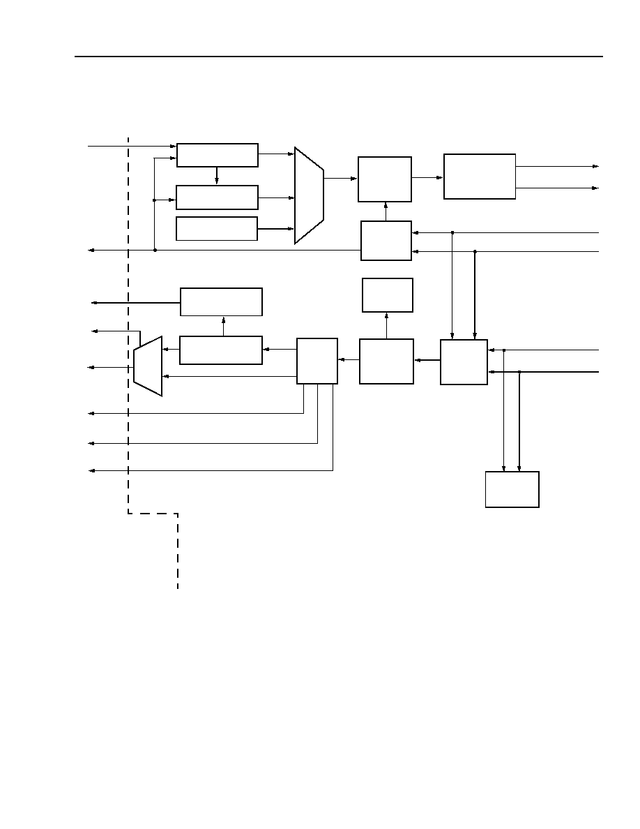
A detailed block diagram of the receive and transmit
data paths for a single channel of the SERDES is
shown in Figure 3.
The transmitter section accepts either 8-bit unencoded
data or 10-bit encoded data at the parallel input port. It
also accepts the low-speed reference clock at the REF-
CLK input and uses this clock to synthesize the internal
high-speed serial bit clock. The serialized data are
available at the differential CML output terminated in
50
or 75
to drive either an optical transmitter or
coaxial media or circuit board/backplane.
The receiver section receives high-speed serial data at
its differential CML input port. These data are fed to the
clock recovery section which generates a recovered
clock and retimes the data. This means that the receive
clocks are asynchronous between channels. The
retimed data are deserialized and presented as a 10-bit
encoded or a 8-bit unencoded parallel data on the out-
put port. Two-phase receive byte clocks are available
synchronous with the parallel words. The receiver also
optionally recognizes the comma characters or code
violations and aligns the bit stream to the proper word
boundary.
Bias Section
A fractional band-gap voltage generator is included on
the design. An external resistor (3.32 k
± 1%), con-
nected between the pins REXT and VSSREXT gener-
ates the bias currents within the chip. This resistor
should be able to handle at least 300 µA.

16
Agere Systems Inc.
Preliminary Data Sheet
July 2001
1.0-1.25/2.0-2.5/3.125 Gbits/s Backplane Interface
ORCA ORT82G5 FPSC Eight-Channel
Backplane Transceiver Core Detailed Description
(continued)
Reset Operation
The SERDES block can be reset in one of three different ways as follows: on power up, using the hardware reset,
or via the microprocessor interface. The power up reset process begins when the power supply voltage ramps up to
approximately 80% of the nominal value of 1.5 V. Following this event, the device will be ready for normal operation
after 3 ms.
A hardware reset is initiated by making the PASB_RESETN low for at least two microprocessor clock cycles. The
device will be ready for operation 3 ms after the low to high transition of the PASB_RESETN. This reset function
affects all SERDES channels and resets all microprocessor and internal registers and counters.
Using the software reset option, each channel can be individually reset by setting SWRST (bit 2) to a logic 1 in the
channel configuration register. The device will be ready 3 ms after the SWRST bit is deasserted. Similarly, all four
channels per quad SERDES can be reset by setting the global reset bit GSWRST. The device will be ready for nor-
mal operation 3 ms after the GSWRST bit is deasserted. Note that the software reset option resets only SERDES
internal registers and counters. The microprocessor registers are not affected. It should also be noted that the
embedded block cannot be accessed until after FPGA configuration is complete.
Start Up Sequence
1.
Initiate a hardware reset by making PASB_RESETN low for 100 ns. The device will be ready for operation 3 ms
after the low to high transition of PASB_RESETN. During this time configure the FPGA portion of the device.
2.
Wait for 100 ns. Configure the following SERDES internal and external registers.
Set the following bits in register 30800:
-- Bits LCKREFN_[AD:AA] to 1, which implies lock to data.
-- Bits ENBYSYNC_[AD:AA] to 1 which enables dynamic alignment to comma.
Set the following bits in register 30801:
-- Bits LOOPENB_[AD:AA] to 1 if loopback is desired.
Set the following bits in register 30900:
-- Bits LCKREFN_[BD:BA] to 1 which implies lock to data.
-- Bits ENBYSYNC_[BD:BA] to 1 which enables dynamic alignment to comma.
Set the following bits in register 30901:
-- Bits LOOPENB_[BD:BA] to 1 if loopback is desired.
Set the following bits in registers 30002, 30012, 30022, 30032, 30102, 30112, 30122, 30132:
-- TXHR[0:3] set to 1 if TX half-rate is desired.
-- 8B10BT[0:1] set to 1
Set the following bits in registers 30003, 30013, 30023, 30033, 30103, 30113, 30123, 30133:
-- RXHR[0:3] Set to 1 if RX half-rate is desired.
-- 8B10BR[0:3] set to 1.
Monitor the following alarm bits in registers 30000, 30010, 30020, 30030, 30110, 30120, 30130:
-- LKI-PLL lock indicator. 1 indicates that PLL has achieved lock.
-- SDON-Signal detect output indicator. 0 indicates active data.
Agere Systems Inc.
17
Preliminary Data Sheet
July 2001
1.0-1.25/2.0-2.5/3.125 Gbits/s Backplane Interface
ORCA ORT82G5 FPSC Eight-Channel
Backplane Transceiver Core Detailed Description
(continued)
2263(F)
Figure 3. SERDES Functional Block Diagram for One Channel
10-BIT REGISTER
8B/10B ENCODER
LINK STATE
8B/10B DECODER
MACHINE
TRANSMIT
PLL
RECEIVE
PLL
SERIAL
TO
PARALLEL
BYTE
ALIGNER
MUX
MUX
PREEMPHASIS
TO/FROM
MUX/DEMUX
BLOCK
HDINP_(A,B)(A-D)
HDINN_(A,B)(A-D)
PARALLEL
TO
SERIAL
HDOUTP_(A,B)(A-D)
HDOUTN_(A,B)(A-D)
REFCLKP_(A,B)
REFCLKN_(A,B)
SRBD(A-D)
[9:0]
SWDSYNC
SRBC0
SRBC1
SBYTSYNC
STBD(A-D)
[9:0]
PRBS GENERATOR
PRBS
CHECKER
ACTIVITY
DETECTOR
STBC311
(A-D)
(A-D)
(A-D)
(A-D)
(A-D)
SCV
(A-D)
18
Agere Systems Inc.
Preliminary Data Sheet
July 2001
1.0-1.25/2.0-2.5/3.125 Gbits/s Backplane Interface
ORCA ORT82G5 FPSC Eight-Channel
Backplane Transceiver Core Detailed Description
(continued)
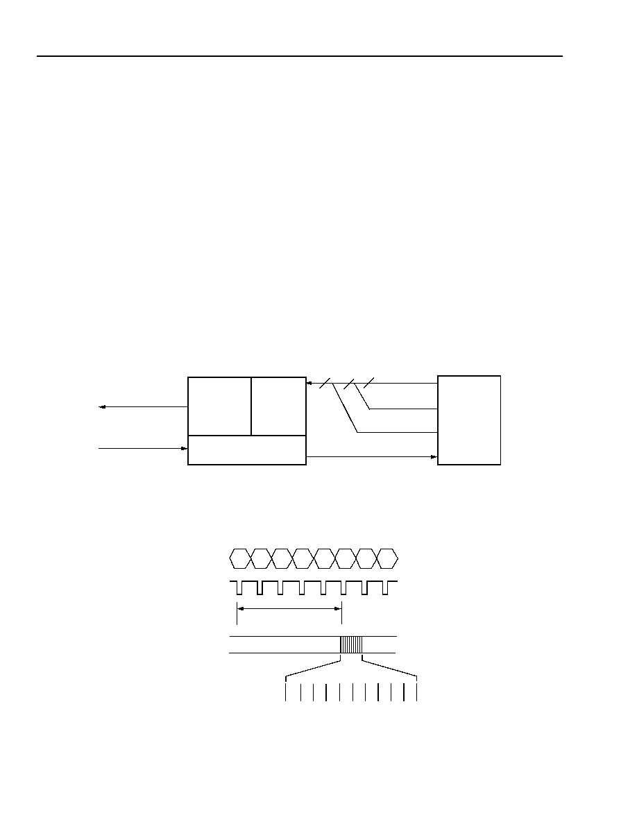
SERDES Transmit Path (FPGA
Backplane)
The transmitter section accepts either 8-bit unencoded data or 10-bit encoded data at the parallel input port from
the MUX/deMUX block. It also accepts the low-speed reference clock at the REFCLK input and uses this clock to
synthesize the internal high-speed serial bit clock.
The serialized data are available at the differential CML output terminated in 50
or 75
to drive either an optical
transmitter, coaxial media, or circuit board/backplane.
The STBDx[8:0] (where x is a placeholder for one of the letters, A--D) ports carry unencoded character data in this
design. The time-division multiplexer in the ORT82G5 is only 9 bits wide. The 10th bit (STBDx[9]) of each data lane
into the SERDES is held constant. It is not possible to use the ORT82G5 for normal data communication without
enabling SERDES 8b/10b encoding.
The functional mode uses the STBCx311 SERDES output as the reference clock. The frequency of this clock will
depend on the half-rate/full-rate control bit in the SERDES; and the frequency of the REFCLK ports and/or that of
the high-speed serial data. The SERDES TBCKSEL control bit must be configured to a 0 for each channel in order
for this clocking strategy to work.
A falling edge on the STBC311x clock port will cause a new data character to be sent from STBDx[9:0] to the SER-
DES block with a latency of 5 STBC311x clock cycles at the high-speed serial output.
2264(F)
Figure 4. ORT82G5 Transmit Path for a Single SERDES Channel
10:1
MULTIPLEXER
100--156 MHz
PLL
8B/10B
ENCODER
CLOCK
TRANSMIT DATA
1.0--3.125 Gbits/s
4:1
MULTIPLEXER
(X 9)
10
8
REFERENCE
EMBEDDED CORE
DATA BYTE
STBDx[7:0]
K-CONTROL
STBDx{8]
9
GROUND
STBDx[9]
STBC311x
SERDES
MUX/DEMUX
HDOUTPx,
HDOUTNx
p
q
r
s
t
x
y
z
STBDx[9:0]
STBC311x
HDOUTx
p
4
p
5
p
6
p
7
p
8
p
9
p
0
p
1
p
2
p
3
LATENCY =
5 STBC311x CLOCKS
BLOCK
BLOCK

Agere Systems Inc.
19
Preliminary Data Sheet
July 2001
1.0-1.25/2.0-2.5/3.125 Gbits/s Backplane Interface
ORCA ORT82G5 FPSC Eight-Channel
Backplane Transceiver Core Detailed Description
(continued)
Transmit Preemphasis and Amplitude Control
The transmitter's CML output buffer is terminated on-chip to optimize the data eye as well as to reduce the number
of discrete components required. The differential output swing reaches a maximum of 1.2 V
PP
in the normal ampli-
tude mode. A half amplitude mode can be selected via configuration register bit HAMP. Half amplitude mode can
be used to reduce power dissipation when the transmission medium has minimal attenuation.
A programmable preemphasis circuit is provided to boost the high frequencies in the transmit data signal to maxi-
mize the data eye opening at the far-end receiver. Preemphasis is particularly useful when the data are transmitted
over backplanes or low-quality coax cables. The degree of preemphasis can be programmed with a two-bit control
from the microprocessor interface as shown in Table 2. The high-pass transfer function of the preemphasis circuit
is shown below, where the value of a is shown in Table 2.
H(z) = (1 ≠ az
≠1
)
Table 2. Preemphasis Settings
SERDES Receive Path (Backplane
FPGA)
The receiver section receives high-speed serial data at its differential CML input port. These data are fed to the
clock recovery section which generates a recovered clock and retimes the data. This means that the receive clocks
are asynchronous between channels. The retimed data are deserialized and presented as a 10-bit encoded or a
8-bit unencoded parallel data on the output port. Two-phase receive byte clocks are available synchronous with the
parallel words. The receiver also recognizes the comma characters and aligns the bit stream to the proper word
boundary.
The receive PLL has two modes of operation as follows: lock to reference and lock to data with retiming. When no
data or invalid data is present on the HDINP and HDINN pins, the receive VCO will not lock to data and its fre-
quency can drift outside of the nominal ±100 ppm range. Under this condition, the receive PLL will lock to REFCLK
for a fixed time interval and then will attempt to lock to receive data. The process of attempting to lock to data, then
locking to clock will repeat until valid input data exists. There is also a control register bit per channel to force the
receive PLL to always lock to the reference clock.
The activity detector monitors the presence of data on each of the differential high-speed input pins. In the absence
of amplitude qualified data on the inputs the chip automatically goes into sleep mode. This function can, however,
be disabled through the control interface.
The PRBS checker is a built-in bit error rate tester (BERT). When enabled, it produces a one-bit PRBSCHK output
to indicate whether there was an error in the loopback data.
PE1
PE0
Amount of Preemphasis (a)
0
0
0% (No Preemphasis)
0
1
12.5%
1
0
12.5%
1
1
25%

20
Agere Systems Inc.
Preliminary Data Sheet
July 2001
1.0-1.25/2.0-2.5/3.125 Gbits/s Backplane Interface
ORCA ORT82G5 FPSC Eight-Channel
Backplane Transceiver Core Detailed Description
(continued)
Data from a SERDES channel appears in 10-bit raw form or 8-bit decoded form at the SRBDx[9:0] port (where x is
a placeholder for one of the letters, A-D) with a latency of approximately 14 cycles. Accompanying this data are the
comma-character indicator (SBYTSYNCx), clocks (SRBC0x, and SRBC1x), link-state indicator (SWDSYNCx), and
code-violation indicator (SCVx).
With the 8B10BR control bit of the SERDES channel set to 1, the data presented at SRBDx[9:0] will be decoded
characters. Bit 8 will indicate whether SRBDx[7:0] represents an ordinary data character (bit 8 == 0), or whether
SRBDx[7:0] represents a special character, like a comma. When 8B10BR is set to 0, the data at SRBDx[9:0] will be
encoded characters. The XAUI link-state machine should not be used in this mode of operation. When in XAUI
mode, the MUX/deMUX looks for /A/ (as defined in IEEE 802.3ae v.2.1) characters for channel alignment and
requires the characters to be in decoded form for this to work.
2265(F)
Figure 5. ORT82G5 Receive Path for a Single SERDES Channel
8B
/
10B
E
NCODE
R
100--156 MHz
PLL & CDR
CLOCK
HDINPx,
RECEIVE DATA
1.0--3.125 Gbits/s
1:4
MULTIPLEXER
(X 10)
XAUI LINK
REFERENCE
EMBEDDED CORE
10:
1
MU
LTI
P
LE
X
E
R
CODE
GRO
U
P
A
L
IGNM
E
NT
L
I
N
K
ST
ATE
MA
CHI
N
E
SRBDx[9:0]
STATE
SBYTSYNCx
SRBC0x
SCVx
MACHINE
25--78 MHZ
CLOCK
COMMADET
4 K_CTRL
32 DATA
MULTI-CHA
N
N
E
L
ALI
G
N
M
EN
T
FIFO
2:1
MULTIPLEXER
(X 40)
DATA
40
DATA
36
SERDES
MUX/DEMUX
CHANNEL ALIGN
SWDSYNCx
SRBC1x
HDINNx
p
q
r
s
t
x
y
z
SRBDx[9:0]
SRBC0x
SRBC1x
SBYTSYNCx,
SVCx
SWDSYNCx
q
0
r
8
r
9
s
0
p
4
p
5
p
6
p
7
p
8
p
9
p
0
p
1
p
2
p
3
r
2
r
3
r
4
r
5
r
6
r
7
s
1
s
2
s
3
s
4
p
HDINx
SRBDx[9:0]
1-bit
10-bit
DE-
BLOCK
BLOCK
BLOCK
LATENCY =
APPROX 23 CLOCKS

Agere Systems Inc.
21
Preliminary Data Sheet
July 2001
1.0-1.25/2.0-2.5/3.125 Gbits/s Backplane Interface
ORCA ORT82G5 FPSC Eight-Channel
Backplane Transceiver Core Detailed
Description
(continued)
8b/10b Encoding/Decoding
The 8b/10b encoder encodes the incoming 8-bit data
into a 10-bit format according to the IEEE 802.3z stan-
dard. Input pins SRBDx<7:0> (where x is a placeholder
for one of the letters, A--D) are used for 8 bit unen-
coded data and SRBDx<8> is used as the K_control
input to indicate whether the 8 data bits need to be
encoded as special characters (K_control = 1) or as
data characters (K_control = 0). When the encoder is
bypassed SRBDx<9:0>serve as the data bits for the
10-bit encoded data.
Within the definition of the 8b/10b transmission code,
the bit positions of the 10-bit encoded transmission
characters are labeled as a, b, c, d, e, i, f, g, h, and j in
that order. Bit a corresponds to SRBDx[0], bit b to
SRBDx[1], bit c to SRBDx[2], bit d to SRBDx[3], bit e to
SRBDx[4], bit i to SRBDx[5], bit f to SRBDx[6], bit g to
SRBDx[7], bit h to SRBDx[8], and bit j to SRBDx[9].
The data SRBDx[9:0] is transmitted serially with
SRBDx[0] transmitted first and SRBDx[9] transmitted
last.
For an 8-bit unencoded data, the 8-bit unencoded data
SRDBx[7:0] is represented as HGF EDCBA SRDBx[8]
represents the K_CTRL bit and SRDBx[9] is unused
(tied to logic 0). SRBDx[0] is still transmitted first and
SRBDx[9] transmitted last.
SERDES Transmit and Receive PLLs
The high-speed transmit and receive serial data can
operate at 1.0--1.25 Gbits/s or 2.0--3.125 Gbits/s
depending on the state of the control bits from the
microprocessor interface. Table 3 shows the relation-
ship between the data rates, the reference clock, and
the transmit TWCKx clocks.
The receiver section receives high-speed serial data at
its differential CML input port. These data are fed to the
clock recovery section which generates a recovered
clock and retimes the data. This means that the receive
clocks are asynchronous between channels. The
retimed data are deserialized and presented as a 10-bit
encoded or a 8-bit unencoded parallel data on the out-
put port. RWCKx receive byte clocks are available syn-
chronous with the parallel words. The receiver also
recognizes the comma characters and aligns the bit
stream to the proper word boundary.
Table 4 shows the relationship between the data rates,
the reference clock, and the RWCKx clocks.
For more information on the reference clock input
requirements and connections to either single ended or
differential inputs, see the LU6X14FT SERDES Macro-
cell Data sheet or the associated reference clock appli-
cation note.
Table 3. Transmit PLL Clock and Data Rates
Note: The selection of full-rate or half-rate for a given reference clock
speed is set by a bit in the transmit control register and can be
set per channel.
Table 4. Receive PLL Clock and Data Rates
Note: The selection of full-rate or half-rate for a given reference clock
speed is set by a bit in the receive control register and can be
set per channel.
Reference Clock
The differential reference clock is distributed to all four
channels. Each channel has a differential buffer to iso-
late the clock from the other channels. The input clock
is preferably a differential signal; however, the device
can operate with a single-ended input. The input refer-
ence clock directly impacts the transmit data eye, so
the clock should have low jitter. In particular, jitter com-
ponents in the dc--5 MHz range should be minimized.
Note: The reference clock, REFCLK, is equivalent to
REFINP and REFINN; throughout the text simply
refer to the reference clock as REFCLK.
Data Rate
Reference
Clock
TCK78[A, B]
Clock
Rate
1.0 Gbits/s
100 MHz
25 MHz
Half
1.25 Gbits/s
125 MHz
31.25 MHz
Half
2.0 Gbits/s
100 MHz
50 MHz
Full
2.5 Gbits/s
125 MHz
62.5 MHz
Full
3.125 Gbits/s
156 MHz
78 MHz
Full
Data Rate
Reference
Clock
RWCKx
Clocks
Rate
1.0 Gbits/s
100 MHz
25 MHz
Half
1.25 Gbits/s
125 MHz
31.25 MHz
Half
2.0 Gbits/s
100 MHz
50 MHz
Full
2.5 Gbits/s
125 MHz
62.5 MHz
Full
3.125 Gbits/s
156 MHz
78 MHz
Full
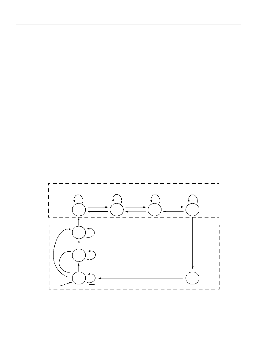
22
22
Agere Systems Inc.
Preliminary Data Sheet
July 2001
1.0-1.25/2.0-2.5/3.125 Gbits/s Backplane Interface
ORCA ORT82G5 FPSC Eight-Channel
Backplane Transceiver Core Detailed
Description
(continued)
Byte Alignment
When ENBYSYNC = 1, the ORT82G5 recognizes the
comma sequence and aligns the 10-bit comma con-
taining character to the word boundary. BYTSYNC = 1
when the parallel output word contains a byte-aligned
comma containing character. The BYTSYNC flag will
continue to pulse a logic 1 whenever a byte aligned
comma containing character is at the parallel output
port.
Link State Machines
Two link state machines are included in the ORT82G5,
one for XAUI applications and a second for fibre-chan-
nel applications.
The fibre-channel link state machine is responsible for
establishing a valid link between the transmitter and the
receiver and for maintaining link synchronization. The
machine wakes up in the loss of synchronization state
upon powerup reset. This is indicated by
WDSYNC = 0. While in this state, the machine looks for
a particular number of consecutive idle ordered sets
without any invalid data transmission in between before
declaring synchronization achieved. Synchronization
achieved is indicated by asserting WDSYNC = 1. Spe-
cifically, the machine looks for three continuous idle
ordered sets without any misaligned comma character
or any running disparity based code violation in
between. In the event of any such code violation, the
machine would reset itself to the ground state and start
its search for the idle ordered sets again.
In the synchronization achieved state, the machine
constantly monitors the received data and looks for any
kind of code violation that might result due to running
disparity errors. If it were to receive four such consecu-
tive invalid words, the link machine loses its synchroni-
zation and once again enters the loss of
synchronization state (LOS). A pair of valid words
received by the machine overcomes the effect of a pre-
viously encountered code violation. LOS is indicated by
the status of WDSYNC output which now transitions
from 1 to 0. At this point the machine attempts to estab-
lish the link yet again. Figure 6 shows the state diagram
for the fibre-channel link state machine.
2266(F)
Figure 6. Fibre-Channel Link State Machine State Diagram
LOS = 1
OS: IDLE ORDERED SET (A 4 CHARACTER BASED WORD HAVING COMMA AS THE 1ST CHARACTER)
VW
RST
LINK SYNCHRONIZATION ACHIEVED (WDSYNC = 1)
OS
CV
OS
OS
OS
CV
CV
CV
CV
CV
VW
VW
VW
2 VW
2 VW
2 VW
a
b
c
d
e
h
g
f
LOSS OF SYNCHRONIZATION (WDSYNC = 0)
LSM_ENABLE
+
POWERUP RESET
VW: VALID WORD (A 4 CHARACTER BASED WORD HAVING NO CODE VIOLATION)
CV: CODE VIOLATION (RUNNING DISPARITY BASED ON ILLEGAL COMMA POSITION)

Agere Systems Inc.
23
Preliminary Data Sheet
July 2001
1.0-1.25/2.0-2.5/3.125 Gbits/s Backplane Interface
ORCA ORT82G5 FPSC Eight-Channel
Backplane Transceiver Core Detailed Description
(continued)
XAUI Link Synchronization Function
For each lane, the receive section of the XAUI link state machine incorporates a synchronization state machine
that monitors the status of the 10-bit alignment. A 10-bit alignment is done in the SERDES based on a comma
character such as K28.5. A comma (0011111 or its complement 1100000) is a unique pattern in the 10-bit space
that cannot appear across the boundary between any two valid 10-bit code-groups. This property makes the
comma useful for delimiting code-groups in a serial stream.This mechanism incorporates a hysteresis to prevent
false synchronization and loss of synchronization due to infrequent bit errors. For each lane, the sync_complete
signal is disabled until the lane achieves synchronization. The synchronization state diagram is shown in Figure 1.
Table 1 and Table 2 describe the state variables used in Figure 1.
Table 5. XAUI Link Synchronization State Diagram Notation--Variables
Table 6. XAUI Link Synchronization State Diagram--Functions
Variable
Description
sync_status
FAIL: Lane is not synchronized (correct 10-bit alignment has not been estab-
lished).
OK: Lane is synchronized.
OK_NOC: Lane is synchronized but a comma character has not been detected
in the past TBD seconds.
enable_CDET
TRUE: Align subsequent 10-bit words to the boundary indicated by the next
received comma.
FALSE: Maintain current 10-bit alignment.
gd_cg
Current number of consecutive cg_good indications.
Function
Description
sync_complete
Indication that alignment code-group alignment has been established at the
boundary indicated by the most recently received comma.
cg_comma
Indication that a valid code-group, with correct running disparity, containing a
comma has been received.
cg_good
Indication that a valid code-group with the correct running disparity has been
received.
cg_bad
Indication that an invalid code-group has been received.
no_comma
Indication that comma timer has expired. The timer is initialized upon receipt of a
comma.
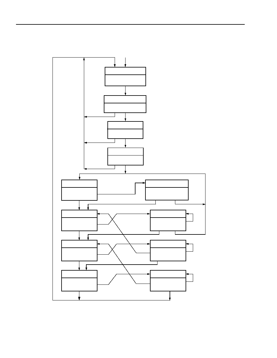
24
Agere Systems Inc.
Preliminary Data Sheet
July 2001
1.0-1.25/2.0-2.5/3.125 Gbits/s Backplane Interface
ORCA ORT82G5 FPSC Eight-Channel
Backplane Transceiver Core Detailed Description
(continued)
2273(F)
Figure 7. XAUI Link Synchronization State Diagram
Loss_of_Sync
sync_status <= FAIL
enable_CDET <= TRUE
sync_complete
reset
Comma_Detect_1
enable_CDET <= FALSE
cg_bad
cg_bad
cg_comma
cg_comma
cg_bad
Comma_Detect_2
Comma_Detect_3
cg_comma
Sync_Aqc'd_1
Sync_Aqc'd_1a
sync_status <= OK
no_comma
sync_status <= OK_NOC
cg_bad
cg_bad
cg_comma
Sync_Aqc'd_2
Sync_Aqc'd_3
Sync_Aqc'd_4
Sync_Aqc'd_2a
Sync_Aqc'd_3a
Sync_Aqc'd_4a
gd_cg <= gd_cg+1
gd_cg <= 0
cg_good
cg_good*
(gd_cg != 3)
cg_bad
cg_good*(gd_cg=3)
cg_good*
(gd_cg != 3)
cg_bad
cg_good*(gd_cg=3)
cg_good
cg_bad
cg_good*(gd_cg=3)
cg_good
cg_good*
(gd_cg != 3)
cg_bad
cg_bad
cg_bad
gd_cg <= 0
gd_cg <= 0
gd_cg <= gd_cg+1
gd_cg <= gd_cg+1
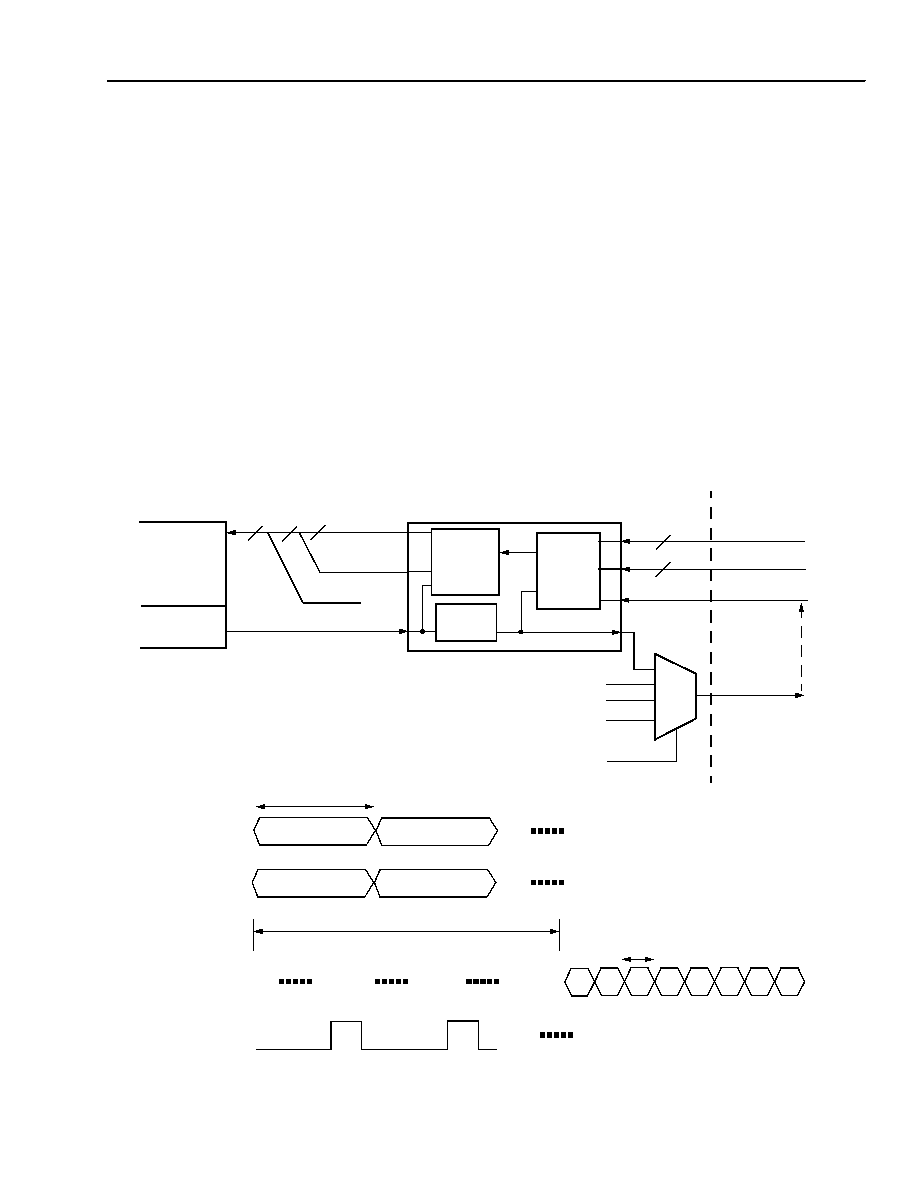
Agere Systems Inc.
25
Preliminary Data Sheet
July 2001
1.0-1.25/2.0-2.5/3.125 Gbits/s Backplane Interface
ORCA ORT82G5 FPSC Eight-Channel
Backplane Transceiver Core Detailed
Description
(continued)
MUX/DeMUX Block
Transmit Path (FPGA
Backplane)
The MUX is responsible for taking 36 bits of data/con-
trol at the low-speed transmit interface and up-convert-
ing it to 9 bits of data/control at the SERDES transmit
interface.
The MUX has 2 clock domains: one based on a clock
received from the SERDES; the other that comes from
the FPGA at 1/4 the frequency of the SERDES clock.
The time sequence of interleaving data/control values
is shown in Figure 8 below.
The low-speed transmit interface consists of a clock,
4 data byte values and a control bit for each of the byte
values. The data bytes are conveyed to the MUX via
the TWDx[31:0] ports. The control bits are TCOM-
MAx[3:0]. The clock is TSYS_CLK(A, B).
Both the data and control are strobed into the MUX at
this interface on the rising edge of TSYS_CLK(A, B).
Besides taking in a clock for capture, the interface
sends back a clock of the same frequency, but arbitrary
phase. This clock, TCK78, is derived from one of the 4
channels of MUX. Within each MUX is a divide-by-4 of
the SERDES TBCx311 clock used in synchronizing the
transmit data words to the TBCx311 clock domain.
TCKSEL[1:0] bits select the source channel of TCK78.
When TCKSEL[1:0] is 00, the clock source is channel
A, 01 is channel B, 10 is channel C, and 11 is channel
D. In many cases, this TCK78 clock is used to drive the
low-speed clock in the FPGA that is connected to the
TSYS_CLK(A, B) signal.
2267(F)
Figure 8. Transmit MUX Block for a Single SERDES Channel
PLL
8B/10B
ENCODER
10
32
4
8
TSYS_CLK(A, B)
TCOMMAx[3:0]
EMBEDDED CORE
FPGA
DATA BYTE
STBDx[7:0]
K-CONTROL
STBDx[8]
9
GROUND
STBDx[9]
STBC311x
SERDES
MUX
p
q
r
s
t
x
y
z
STBDx[9:0]
TCOMMAx[3:0]
LATENCY = 4 TSYS_CLK (A, B) CLOCKS
TWDx[31:0]
PARALLEL
TO
SERIAL
(X 9)
DIVIDE
BY 4
FIFO
MUX
4 CHANNELS
TCKSEL[1:0]
TCK78(A,B)
TWDx[31:0]
TSYS_CLK (A, B)
p
7-0
p
8
40-bit
q
7-0
r
7-0
s
7-0
t
7-0
x
7-0
y
7-0
z
7-0
s
8
q
8
r
8
t
8
z
8
x
8
y
8
10-bit (THE MSB ALWAYS TIED TO LOGIC 0)
BLOCK
BLOCK
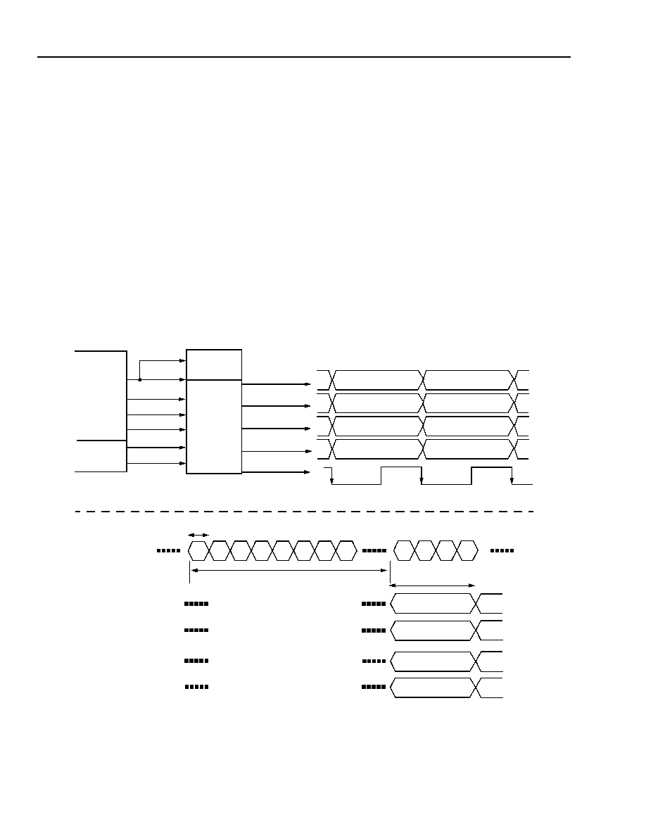
26
26
Agere Systems Inc.
Preliminary Data Sheet
July 2001
1.0-1.25/2.0-2.5/3.125 Gbits/s Backplane Interface
ORCA ORT82G5 FPSC Eight-Channel
Backplane Transceiver Core Detailed
Description
(continued)
Receive Path (Backplane
FPGA)
The deMUX has to accumulate four sets of characters
presented to it at the SERDES receive interface and
put these out at one time at the low-speed receive
interface.
Another task of the deMUX is to recognize the synchro-
nizing event and adjust the 4-byte boundary so that the
synchronizing character leads off a new 4-byte word.
This feature will be referred to as word alignment in
other areas of this document. Word alignment will only
occur when the communication channel is synchro-
nized. When there is no synchronization of the link, the
deMUX will continue to output 4-byte words at some
arbitrary, but constant, boundary.
The deMUX passes on to the channel alignment FIFO
block a set of control signals that indicate the location
of the synchronizing event. RCOMMAx[3:0] are these
indicators. If there is no link synchronization, all of the
RCOMMAx[3:0] bits will be 0s independent of synchro-
nizing events that come in. When the link is synchro-
nized, then the bit that corresponds to the time of the
synchronization event will be set to a 1.
The relationship between a time sequence of values
input at SRBDx[7:0] to the values output at RWDx[31:0]
is shown in Figure 9 below. A parallel relationship
exists between SRBDx[8] and RWBIT8x[3:0] as well as
between SRBDx[9] and RWBIT9x[3:0].
2268(F)
Figure 9. Receive DeMUX Block for a Single SERDES Channel
8B
/
10B
E
NCODE
R
PLL & CDR
1:4
DEMUX
(X 10)
XAUI LINK
SRBDx[9:0]
STATE
SBYTSYNCx
SRBC0x
SCVx
MACHINE
RWCKx
RCOMMAx[3:0]
RWBIT8x[3:0]
RWBIT9x[3:0]
SERDES
DEMUX
SWDSYNCx
SRBC1x
p
q
r
s
t
x
y
z
SRBDx[7:0]
10-bit
RWDx[31:0]
p
7-0
q
7-0
r
7-0
s
7-0
t
7-0
x
7-0
y
7-0
z
7-0
p
8
s
8
q
8
r
8
t
8
z
8
x
8
y
8
p
9
s
9
q
9
r
9
t
9
z
9
x
9
y
9
p
c
s
c
q
c
r
c
t
c
z
c
x
c
y
c
p
q
r
s
t
x
y
z
40-bit
RWDx[31:24]
RWDx[23:16]
RWDx[15:8]
RWDx[7:0]
BLOCK
BLOCK
LATENCY = 4 RWCKx CLOCKS
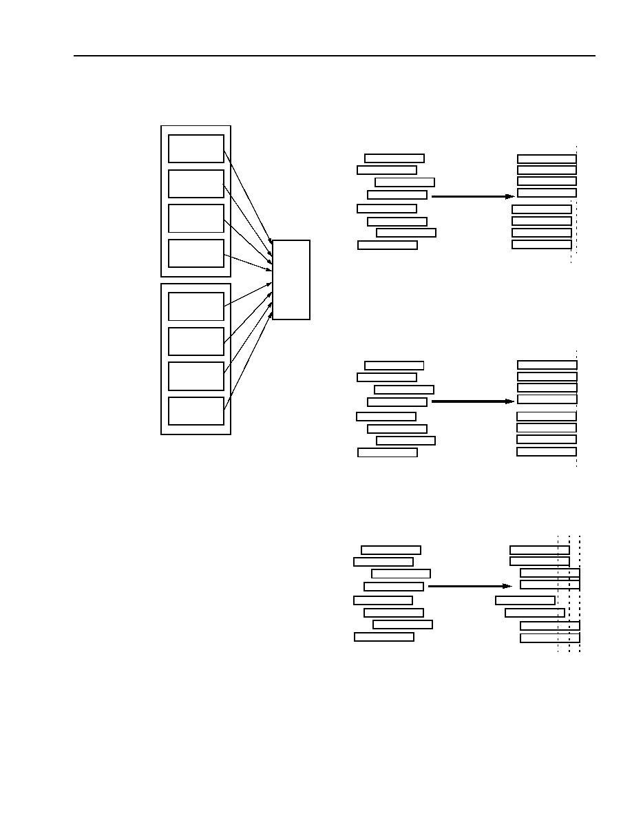
Agere Systems Inc.
27
Preliminary Data Sheet
July 2001
1.0-1.25/2.0-2.5/3.125 Gbits/s Backplane Interface
ORCA ORT82G5 FPSC Eight-Channel
Backplane Transceiver Core Detailed
Description
(continued)
5-8577 (F)
Figure 10. Interconnect of Streams for FIFO
Alignment
Multichannel Alignment (Backplane
FPGA)
The alignment FIFO allows the transfer of all data to
the system clock. The FIFO sync block (Figure 10)
allows the system to be configured to allow the frame
alignment of multiple slightly varying data streams. This
optional alignment ensures that matching SERDES
streams will arrive at the FPGA end in perfect data
sync.
The ORT82G5 has a total of 8 channels (4 per SER-
DES). The incoming data of these channels can be
synchronized in several ways, or they can be indepen-
dent of one other. For example, all four channels in a
SERDES can be aligned together to form a communi-
cation channel with a bandwidth of 10 Gbits/s as shown
in Figure 11.
Optionally, the alignment can be extended across SER-
DES to align all 8 channels in ORT82G5 as shown in
Figure 12. Individual channels within an alignment
group can be disabled (i.e., power down) without dis-
rupting other channels.
Alternatively, two channels within a SERDES can be
aligned together; channel A and B and/or channel C
and D can form a pair as shown in Figure 13.
0673(F)
Figure 11. Example of SERDES A Alignment and
SERDES B Alignment
0674
Figure 12. Example of SERDES A and B Alignment
0675
Figure 13. Example of Multiple Twin Channel
Alignment
SERDES A
STREAM A
SERDES A
STREAM B
SERDES A
STREAM C
SERDES A
STREAM D
SERDES B
STREAM A
SERDES B
STREAM B
SERDES B
STREAM C
FIFO
SYNC
SERDES B
STREAM D
SERDES A
SERDES B
SERDES A Stream A
ALL 4 ALIGNMENT OF SERDES A AND SERDES B
t
0
t
1
SERDES A Stream B
SERDES A Stream C
SERDES A Stream D
SERDES B Stream D
SERDES B Stream C
SERDES B Stream B
SERDES B Stream A
SERDES B Stream D
SERDES B Stream C
SERDES B Stream B
SERDES B Stream A
SERDES A Stream A
SERDES A Stream B
SERDES A Stream C
SERDES A Stream D
ALL 8 ALIGNMENT OF SERDES A AND SERDES B
t
0
SERDES A Stream A
SERDES A Stream B
SERDES A Stream C
SERDES A Stream D
SERDES B Stream D
SERDES B Stream C
SERDES B Stream B
SERDES B Stream A
SERDES A Stream A
SERDES A Stream B
SERDES A Stream C
SERDES A Stream D
SERDES B Stream D
SERDES B Stream C
SERDES B Stream B
SERDES B Stream A
TWO CHANNEL ALIGNMENT
t
1
t
2
SERDES A Stream A
SERDES A Stream B
SERDES A Stream C
SERDES A Stream D
SERDES B Stream D
SERDES B Stream C
SERDES B Stream B
SERDES B Stream A
t
0
SERDES B Stream D
SERDES B Stream C
SERDES B Stream B
SERDES B Stream A
SERDES A Stream A
SERDES A Stream B
SERDES A Stream C
SERDES A Stream D
TWIN ALIGNMENT OF STREAM A & B OF SERDES A
TWIN ALIGNMENT OF STREAM C & D OF SERDES A
TWIN ALIGNMENT OF STREAM C & D OF SERDES B
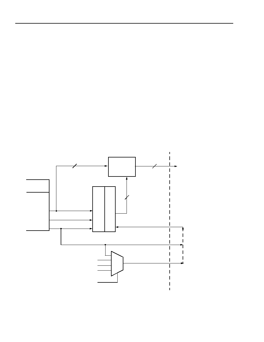
28
Agere Systems Inc.
Preliminary Data Sheet
July 2001
1.0-1.25/2.0-2.5/3.125 Gbits/s Backplane Interface
ORCA ORT82G5 FPSC Eight-Channel
Backplane Transceiver Core Detailed Description
(continued)
The multiplexed, receive word outputs to the FPGA are shown in Figure 14. These are each 40 bits wide. There are
eight of these interfaces, one for each data lane. Each consist of four 10-bit characters, or four decoded characters
(each 8 bits + 1 bit K_CTRL) + CH248_SYNCx status indicator bit depending on setting of NOCHALGNx control
register bits. Note that there is one control bit for a bank of channels, for a total of two control bits. Also, note that
while 10 bits are provided for each character when NOCHALGNx = 1, only the lower 9 bits of each character will be
meaningful if the 8B10BR bit is configured to 1 for that SERDES channel.
With x representing the bank (placeholder for A or B) and y representing the channel (placeholder for A, B, C, or D)
the 40-bit MRWDxy[39:0] is allocated as in Table x.
In the receive path, each channel is provided with a 24 word x 36-bit FIFO. The FIFO can perform two tasks: (1) to
change the clock domain from receive clock to a clock from the FPGA side, and (2) to align the receive data over 2,
4, or 8 channels. The input to the FIFO consists of 36-bit demultiplexed data, RWBYTESYNC[3:0], RWDx[31:0],
and RWBIT8x[3:0].
The four RWBYTESYNC bits are control signals, e.g., they can be the COMMADET signals indicating the presence
of COMMA character. The other 32 RWD bits are the 4 characters from the 8b/10b decoder. The RWBIT8 indicates
the presence of Km.n control character in the receive data byte. Only RWBIT8 and RWD inputs are stored in the
FIFO. During alignment process, RWBYTESYNC is used to synchronize multiple channels. If a channel is not in
any alignment group, it will set the FIFO-write-address to the beginning of the FIFO, and will set the FIFO-read-
address to the middle of the FIFO, at the first assertion of RWBYTESYNC after reset or after the resync command.
2269(F)
Figure 14. Multichannel Alignment FIFO Block for a Single SERDES Channel
1:4
DEMUX
(X 10)
XAUI LINK
STATE
MACHINE
RWCKx
RWBYTESYNC[3:0]
DEMUX
RWDx[31:0]
40
MRWDx
RWCKx
FPGA
M
U
LTI
-
C
H
A
NNE
L
AL
I
G
N
M
E
N
T
FIFO
2:1
MULTIPLEXER
(X 40)
40
36
CHANNEL ALIGN
EMBEDDED CORE
MUX
4 CHANNELS
RCKSEL[1:0]
RCK78(A,B)
RSYS_CLK(A,B)
(FROM GLOBAL OR
SECONDARY FPGA
CLOCK NETWORKS)
(TO LOCAL FPGA
SECONDARY CLOCK
NETWORK)
(TO GLOBAL FPGA
SYSTEM CLOCK
NETWORK)

Agere Systems Inc.
29
Preliminary Data Sheet
July 2001
1.0-1.25/2.0-2.5/3.125 Gbits/s Backplane Interface
ORCA ORT82G5 FPSC Eight-Channel
Backplane Transceiver Core Detailed
Description
(continued)
The use of the FIFO is controlled by configuration bits,
and the raw demultiplexed data can also be sent to the
FPGA directly, by passing the alignment FIFO. The
control register bits for alignment FIFO in ORT82G5
are described below.
Table 7. Multichannel Alignment Modes
where xx is one of A[A:D] and B[A:D].
To align all eight channels:
s
FMPU_SYNMODE_A[A:D] = 11
s
FMPU_SYNMODE_B[A:D] = 11
To align all four channels in SERDES A:
s
FMPU_SYNMODE_A[A:D] = 10
To align two channels in SERDES A:
s
FMPU_SYNMODE_A[A:B] = 01 for channel AA and
AB
s
FMPU_SYNMODE_A[C:D] = 01 for channel AC and
AD
Similar alignment can be defined for SERDES B.
To enable/disable synchronization signal of individual
channel within a multi-channel alignment group:
s
FMPU_STR_EN_xx = 1 enabled
s
FMPU_STR_EN_xx = 0 disabled
where xx is one of A[A:D] and B[A:D].
To re-synchronize a multi-channel alignment group set
the following bit to zero, and then set it to 1.
s
FMPU_RESYNC8 for eight channel A[A:D] and
B[A:D]
s
FMPU_RESYNC4A for quad channel A[A:D]
s
FMPU_RESYNC2A1 for twin channel A[A:B]
s
FMPU_RESYNC2A2 for twin channel A[C:D]
s
FMPU_RESYNC4B for quad channel B[A:D]
s
FMPU_RESYNC2B1 for twin channel B[A:B]
s
FMPU_RESYNC2B2 for twin channel B[C:D]
To resynchronize an independent channel (resetting
the write and the read pointer of the FIFO) set the fol-
lowing bit to zero, and then set it to 1.
s
FMPU_RESYNC1_xx where xx is one of A[A:D] and
B[A:D]
A two-to-one multiplexor is used to select between
aligned or nonaligned data to be sent to the FPGA on
MRWDxy[39:0]. With x representing the bank (place-
holder for A or B) and y representing the channel
(placeholder for A, B, C or D), the 40-bit MRWDxy[39:0]
is allocated as shown in Table 8.
Alignment Sequence
1.
Follow steps 1 and 2 in the start up sequence
described previously.
2.
Initiate a SERDES software reset by setting the
SWRST bit to 1 and then to 0. Note that, any
changes to the SERDES configuration bits should
be followed by a software reset.
3.
Wait for 3 ms. REFCLK_[P, N] should be toggling
by this time. During this time, configure the follow-
ing registers.
Set the following bits in registers 30820, 30920
s
XAUI_MODEx-set to 1 for XAUI mode or keep the
default value of 0.
Enable channel alignment by setting sync bits in
registers 30811, 30911
s
FMPU_SYNMODE_xx. Set to appropriate val-
ues for 2, 4, or 8 alignment.
Set RCLKSELx and TCKSELx bits in registers
30A00.
s
RCKSELx-choose clock source for 78 MHz
RCK78x.
s
TCKSELx-Choose clock source for 78 MHz
TCK78x.
4.
Send data on serial links. Monitor the following sta-
tus/alarm bits:
Monitor the following alarm bits in registers 30000,
30010, 30020, 30030, 30100, 30110, 30120,
30130.
s
LKI-PLL lock indicator. A 1 indicates that PLL has
achieved lock.
s
SDON-signal detect output indicator. A 0 indi-
cates active data.
Monitor the following status bits in registers 30804,
30904
s
XAUISTAT_xx-In XAUI mode, they should be 01
or 10.
Register Bits
FMPU_SYNMODE_xx
Mode
00
No multichannel alignment.
01
Twin channel alignment.
10
Quad channel alignment.
11
Eight channel alignment.
30
Agere Systems Inc.
Preliminary Data Sheet
July 2001
1.0-1.25/2.0-2.5/3.125 Gbits/s Backplane Interface
ORCA ORT82G5 FPSC Eight-Channel
Backplane Transceiver Core Detailed Description
(continued)
Monitor the following status bits in registers 30805, 30905
s
DEMUXWAS_xx-They should be 1 indicating word alignment is achieved.
s
CH248_SYNCxx-They should be 1 indicating channel alignment. this is cleared by resync.
5.
Write a 1 to the appropriate resync registers 30820, 30920. Note that this assumes that the previous value of
the resync bits are 0. The resync operation requires a rising edge. Two writes are required to the resync bits:
write a 0 and then write a 1.
Check out-of-sync and FIFO overflow status in registers 30814 (Bank A).
s
SYNC4_A_OOS, SYNC4_A_OVFL-by 4 alignment.
s
SYNC2_A2_OOS, SYNC_A2_OVFL or SYNC2_A!_OOS, SYNC2_A!_OVFL-by 2 alignment.
Check out-of-sync status in registers 30914 (Bank 4).
s
SYNC4_B_OOS, SYNC4_B_OVFL-by 4 alignment.
s
SYNC_B2_OOS, SYNC2_B2_OVFL or SYNC2_B1_OOS, SYNC_B1_OVFL-by 2 alignment.
Check out-of-sync status in register 30A03
s
SYNC8_OOS, SYNC8_OVFL-by 8 alignment.
If out-of-sync bit is 1 or FIFO overflow is 1 then rewrite a 1 to the appropriate resync registers and monitor the
OOS and OVFL bits again. The resync operation requires a rising edge. Two writes are required to the resync
bits: write a 0 and then write a 1.
Alignment can also be done between the receive channels on two ORT82G5 devices. Each of the two devices
needs to provide its aligned K_CTRL or other alignment character to the other device, which will delay reading
from a second alignment FIFO until all channels requesting alignment on the current device AND all channels
requesting alignment on the other device are aligned (as indicated on the K_CTRL character). This second
alignment FIFO will be implemented in FPGA logic on the ORT82G5. This scheme also requires that the refer-
ence clock for both devices be driven by the same signal.
XAUI Lane Alignment Function (Lane Deskew)
In XAUI mode, the receive section in each lane uses the /A/ code group to compensate for lane-to-lane skew. The
mechanism restores the timing relationship between the 4 lanes by lining up the /A/ characters into a column. Fig-
ure 2 shows the alignment of four lanes based on /A/ character. A minimum spacing of 16 code-groups implies that
at least ± 80 bits of skew compensation capability should be provided, which the ORT82G5 significantly exceeds.
2392(F)
Figure 15. De-Skew Lanes by Aligning /A/ Columns
LANE 0
K
R
R
K
R
K
R
K
K
R
K
R
R
K
A
LANE 1
K
R
R
K
R
K
R
K
K
R
K
R
R
K
A
LANE 2
K
R
R
K
R
K
R
K
K
R
K
R
R
K
A
LANE 3
K
R
R
K
R
K
R
K
K
R
K
R
R
K
A
LANE 0
K
R
R
K
R
K
R
K
K
R
K
R
R
K
A
LANE 1
K
R
R
K
R
K
R
K
K
R
K
R
R
K
A
LANE 2
K
R
R
K
R
K
R
K
K
R
K
R
R
K
A
LANE 3
K
R
R
K
R
K
R
K
K
R
K
R
R
K
A

Agere Systems Inc.
31
Preliminary Data Sheet
July 2001
1.0-1.25/2.0-2.5/3.125 Gbits/s Backplane Interface
ORCA ORT82G5 FPSC Eight-Channel
Backplane Transceiver Core Detailed Description
(continued)
Table 8. Definition of Bits of MRWDxy[39:0]
Bit Index
NOCHALGNx = 1
NOCHALGNx = 0
39
b9 of char 1
CH248_SYNCx
38
b8 of char 1
K_CTRL for char 1
37
b7 of char 1
b7 of char 1
36
b6 of char 1
b6 of char 1
35
b5 of char 1
b5 of char 1
34
b4 of char 1
b4 of char 1
33
b3 of char 1
b3 of char 1
32
b2 of char 1
b2 of char 1
31
b1 of char 1
b1 of char 1
30
b0 of char 1
b0 of char 1
29
b9 of char 2
n/c
28
b8 of char 2
K_CTRL for char 2
27
b7 of char 2
b7 of char 2
26
b6 of char 2
b6 of char 2
25
b5 of char 2
b5 of char 2
24
b4 of char 2
b4 of char 2
23
b3 of char 2
b3 of char 2
22
b2 of char 2
b2 of char 2
21
b1 of char 2
b1 of char 2
20
b0 of char 2
b0 of char 2
19
b9 of char 3
n/c
18
b8 of char 3
K_CTRL for char 3
17
b7 of char 3
b7 of char 3
16
b6 of char 3
b6 of char 3
15
b5 of char 3
b5 of char 3
14
b4 of char 3
b4 of char 3
13
b3 of char 3
b3 of char 3
12
b2 of char 3
b2 of char 3
11
b1 of char 3
b1 of char 3
10
b0 of char 3
b0 of char 3
09
b9 of char 4
n/c
08
b8 of char 4
K_CTRL for char 4
07
b7 of char 4
b7 of char 4
06
b6 of char 4
b6 of char 4
05
b5 of char 4
b5 of char 4
04
b4 of char 4
b4 of char 4
03
b3 of char 4
b3 of char 4
02
b2 of char 4
b2 of char 4
01
b1 of char 4
b1 of char 4
00
b0 of char 4
b0 of char 4

32
Agere Systems Inc.
Preliminary Data Sheet
July 2001
1.0-1.25/2.0-2.5/3.125 Gbits/s Backplane Interface
ORCA ORT82G5 FPSC Eight-Channel
Backplane Transceiver Core Detailed Description
(continued)
Loopback Modes
The device can be exercised in four possible loopback modes. These loopback modes are identified as:
s
High-speed serial loopback
s
Parallel loopback at the SERDES boundary
s
Parallel loopback at MUX/deMUX boundary excluding SERDES
s
Operational mode full loopback using the PRBS generator/checker
These four loopback modes are described next.
High-Speed Serial Loopback
The high-speed serial loopback involves the transmit signal at the serial interface being looped back internally to
the receive circuitry. The serial loopback path does not include the high-speed input and output buffers. The
HDOUTP, HDOUTN outputs are active in this loopback mode, but the CML input buffers are powered down. The
data are sourced at the LDIN[9:0] pins and detected at the LDOUT[9:0] pins. The device is otherwise in its normal
mode of operation. The data rate selection bits, TXHR and RXHR, in the channel configuration registers must be
configured to carry the same value and the PRBS Generator and Checker are excluded by setting the PRBS con-
figuration bit to 0. The 8b/10b encoder/decoder can optionally be configured into or out of the loopback path. The
following Table 9 illustrates the control interface register configuration for the high-speed serial loopback.
Table 9. High-Speed Serial Loopback Configuration
Register
Address
Bit Value
Bit Name
Comments
30002, 30012, 30022,
30032, 30102, 30112,
30122, 30132
Bit 0 = 0 or 1
TXHR
Set to 0 or 1. TXHR and RXHR bits must be set to the
same value.
30002, 30012, 30022,
30032, 30102, 30112,
30122, 30132
Bit 7 = 0 or 1
8B10BT
Set to 0 or 1. If set to 0, the 8b/10b encoder is excluded
from the loopback path. The 8b/10b encoder and decoder
selection control bits must both be set to the same value.
30003, 30013, 30023,
30033, 30103, 30113,
30123, 30133
Bit 0 = 0 or 1
RXHR
Set to 0 or 1. TXHR and RXHR bits must be set to the
same value.
30003, 30013, 30023,
30033, 30103, 30113,
30123, 30133
Bit 3 = 0 or 1
8B10BR
Set to 0 or 1. If set to 0, the 8b/10b decoder is excluded
from the loopback path. The 8b/10b encoder and decoder
selection control bits must both be set to the same value.
30004, 30014, 30024,
30034, 30104, 30114,
30124, 30134
Bit 0 = 0
PRBS
Set to 0.
30004, 30014, 30024,
30034, 30104, 30114,
30124, 30134
Bit 7 = 1
TESTEN
Set to 1 if the loopback is done on a per-channel basis.
However, if the loopback is done globally on all the four
channels, this bit can be set to 0 but bit 7 of register 5
must be set to 1.
30005, 30105
Bit 7 = 1
GTESTEN
Set to 1 if the loopback is done globally on all four
channels.
30006, 30106
Bits[4:0] =
00000
--
Set to 00000.

Agere Systems Inc.
33
Preliminary Data Sheet
July 2001
1.0-1.25/2.0-2.5/3.125 Gbits/s Backplane Interface
ORCA ORT82G5 FPSC Eight-Channel
Backplane Transceiver Core Detailed Description
(continued)
Parallel Loopback at the SERDES Boundary
The parallel loopback involves the parallel buses LDIN[9:0] and LDOUT[9:0]. The loopback connection is made
such that LDIN[9:0] is logically equivalent to LDOUT[9:0]. In the parallel loopback mode, the LDOUT[9:0] pins
remain active. The receive data are sourced at the HDINP, HDINN pins and detected at the HDOUTP, HDOUTN
pins. The device is otherwise in its normal mode of operation. The data rate selection bits TXHR and RXHR in the
channel configuration registers must be configured to carry the same value and the PRBS generator and checker
are excluded by setting the PRBS configuration bit to 0. Also, the 8b/10b encoder and decoder are excluded from
the loopback path by setting the 8b10bT and 8b10bR configuration bits to 0. Table 10 illustrates the control inter-
face register configuration for the parallel loopback.
Table 10. Parallel Loopback Configuration
Parallel Loopback at MUX/DeMUX Boundary Excluding SERDES
This is a low-frequency testmode. This parallel loopback involves the parallel buses SRBDx[9:0] and STBDx[9:0].
The loopback connection is made such that SRBDx[9:0] is logically equivalent to STBDx[9:0] and STBDx[9:0]
remains active, thus bypassing the SERDES. Data can be sent from the FPGA through TWDxx signals and moni-
tored on MRWDxx signals. This test is enabled by setting the pin PLOOP_TEST_ENN to 1. PASB_TESTCLK must
be running in this mode at 4x frequency of RSYS_CLK[A, B] or TSYS_CLK[A, B].
Register
Address
Bit Value
Bit Name
Comments
30002, 30012, 30022, 30032,
30102, 30112, 30122, 30132
Bit 0 = 0 or 1
TXHR
Set to 0 or 1. TXHR and RXHR bits must be set to
the same value.
30002, 30012, 30022, 30032,
30102, 30112, 30122, 30132
Bit 7 = 0
8B10BT
Set to 0. The 8b/10b encoder is excluded from the
loopback path. The 8b/10b encoder and decoder
selection control bits must both be set to 0.
30003, 30013, 30023, 30033,
30103, 30113, 30123, 30133
Bit 0 = 0 or 1
RXHR
Set to 0 or 1. TXHR and RXHR bits must be set to
the same value.
30003, 30013, 30023, 30033,
30103, 30113, 30123, 30133
Bit 3 = 0
8B10BR
Set to 0. The 8b/10b decoder is excluded from the
loopback path. The 8b/10b encoder and decoder
selection control bits must both be set to 0.
30004, 30014, 30024, 30034,
30104, 30114, 30124, 30134
Bit 0 = 0
PRBS
Set to 0.
30004, 30014, 30024, 30034,
30104, 30114, 30124, 30134
Bit 7 = 1
--
Set to 1 if the loopback is done on a per-channel
basis.
However, if the loopback is done globally on all
the four
channels, this bit can be set to 0 but bit 7 of regis-
ter 5
must be set to 1.
30005, 30105
Bit 7 = 1
--
Set to 1 if the loopback is done globally on all four
channels.
30006, 30106
Bits[4:0] =00001
--
Set to 00001.

34
Agere Systems Inc.
Preliminary Data Sheet
July 2001
1.0-1.25/2.0-2.5/3.125 Gbits/s Backplane Interface
ORCA ORT82G5 FPSC Eight-Channel
Backplane Transceiver Core Detailed Description
(continued)
Operational Mode Full Loopback Test Using The PRBS Generator/Checker
The operational mode full loopback test forms one of the normal operational modes of the device. The loopback
can be either internal to the device or external to it. To perform the test with internal loopback, the LOOPENB pin
should be set to a logic 1. The test includes the PRBS generator in the transmit path and the PRBS checker in the
receive path. In this case, the device is placed in its normal operational mode with all the functional blocks in the
transmit and the receive path active. The transmit data is generated by an LFSR. The generated word is then seri-
alized and looped back (either internally or externally) to the receiver. The receiver first deserializes the 8-bit word
to regenerate the transmitted 8-bit word. The PRBS checker on the receiver compares the regenerated 8-bit word
against the transmitted 8-bit word on a word by word basis and signals a mismatch by asserting a PRBSCHK alarm
status bit. During this test, the receiver regenerated 8-bit words can also be observed on the device output ports.
The PRBS checker contains a watchdog timer which asserts the time-out alarm status bit, PRBSTOUT, if the
PRBS test cannot progress beyond its start state within a reasonable time interval. This time interval is set by the
precision of the watchdog timer. Both the PRBSCHK and the PRBSTOUT alarms can generate an interrupt if their
corresponding masks are disabled.
ASB Memory Blocks
This section describes the memory blocks in the embedded core. Note that although the memory blocks are in the
embedded core part of the chip, they do not interact with the rest of the embedded core circuits. They are stand-
alone blocks designed specifically to increase RAM capacity in the ORT82G5 chip, and will be used by the soft IP
cores in the FPGA.
There are two independent memory blocks in the embedded core. These are in addition to the block RAMs found in
the FPGA portion of the ORT82G5. A block diagram of a memory block is shown in Figure 16. Each memory block
has a capacity of 4K word by 36 bit. It has one read port and one write port and four byte-write-enable (active-low)
signals. The read data from the memory block is registered so that it works as a pipelined synchronous memory
block. A block diagram of the memory block in shown below in Figure 16.The minimum timing specifications are
shown in Figure 18.
2270(F)
Figure 16. Block Diagram of Memory Block
4K x 36
MEMORY BLOCK
(1 OF 2)
D_x[35:0]
CKW_x
CSWA_x
CSWB_x
AW_x[10:0]
BYTEWN_x[3]
BYTEWN_x[2]
BYTEWN_x[1]
BYTEWN_x[0]
BW[35,31:24]
BW[34,23:16]
BW[33,15:8]
BW[32,7:0]
CKR_x
CSR_x
AR_x[10:0]
Q_x[35:0]
WRITE PORTS
READ PORTS

Agere Systems Inc.
35
Preliminary Data Sheet
July 2001
1.0-1.25/2.0-2.5/3.125 Gbits/s Backplane Interface
ORCA ORT82G5 FPSC Eight-Channel
Backplane Transceiver Core Detailed Description
(continued)
2271(F)
Figure 17. Minimum Timing Specs for Memory Blocks-Write Cycle
2272(F)
Figure 18. Minimum Timing Specs for Memory Blocks-Read Cycle
CSW[A,B]
AW[10:0]
CKW
D[35:0]
BYTEWN[3:0]
1.5 ns
2.0 ns
0.5 ns
0.3 ns
0.5 ns
0.3 ns
0.5 ns
0.3 ns
0.7 ns
0.3 ns
CKR
AR[10:0],
CSR
Q[35:0]
1.5 ns
1.5 ns
4.5 ns
0.5 ns
2.0 ns
0 ns

36
Agere Systems Inc.
Preliminary Data Sheet
July 2001
1.0-1.25/2.0-2.5/3.125 Gbits/s Backplane Interface
ORCA ORT82G5 FPSC Eight-Channel
Memory Map
Definition of Register Types
The registers in ORT82G5 are 8-bit memory locations, which in general can be classified into the following types:
Status Register and Control Register.
Status Register
Read-only register to convey the status information of various operations within the FPSC core. An example is the
state of the XAUI link-state-machine.
Control Register
Read-write register to set up the control inputs that define the operation of the FPSC core.
The SERDES block within the ORT82G5 core has a set of status and control registers for it's operation. The
detailed description of them can be found in the SERDES data sheet.
There is another group of status and control registers which are implemented outside the SERDES, which are
related to the SERDES and other functional blocks in the FPSC core. They will be described in detail here. Each
SERDES has four independent channels, which are named A, B, C, or D. Using this nomenclature, the SERDES A
channels are named as AA, AB, AC, and AD, while SERDES B channels will be BA, BB, BC, and BD.
Table 11. Structural Register Elements
A full memory map is included in Table 12.
Address (Hex)
Description
300xx
SERDES A, internal registers.
301xx
SERDES B, internal registers.
308xx
Channel A [A:D] registers (external to SERDES blocks).
309xx
Channel B [A:D] registers (external to SERDES blocks).
30A0x
Global registers (external to SERDES blocks).

Agere Systems Inc.
37
Preliminary Data Sheet
July 2001
1.0-1.25/2.0-2.5/3.125 Gbits/s Backplane Interface
ORCA ORT82G5 FPSC Eight-Channel
Memory Map
(continued)
Table 12 details the memory map for the ASIC core of the ORT82G5 device. This table shows the databus oriented
for the PPC interface. DB0 is the MSB, while DB7 is the LSB. If the user master interface is used to preform opera-
tions to the ASIC core then the databus must be used in the opposite notation, where DB7 is the MSB and DB0 is
the LSB.
Table 12. Memory Map
Addr
(Hex)
Reg
#
DB0
DB1
DB2
DB3
DB4
DB5
DB6
DB7
Default
Value
SERDES A Alarm Registers (Read Only)
30000
SDON_AA
Receive Signal
Detect Output, Bank
A, Channel A. When
SDON_AA = 0, then
active data is
present.
LKI_AA
Receive PLL Lock
Indication, Bank A,
Channel A. When
LKI_AA = 1, then
PLL receive is
locked.
PRBSCHK_AA
PRBS Check Pass/
Fail Indication, Bank
A, Channel A. When
PRBSCHK_AA = 0,
then it is a pass indi-
cation.
PRBSTOUT_AA
PRBS Checker Watch-
dog Timer Time-Out
Alarm, Bank A, Channel
A. When
PRBSTOUT_AA = 1,
then timeout has
occurred.
--
--
--
--
00
30010
SDON_AB
Receive Signal
Detect Output, Bank
A, Channel B. When
SDON_AB = 0, then
active data is
present.
LKI_AB
Receive PLL Lock
Indication, Bank A,
Channel B. When
LKI_AB = 1, then
PLL receive is
locked.
PRBSCHK_AB
PRBS Check Pass/
Fail Indication, Bank
A, Channel B. When
PRBSCHK_AB = 0,
then it is a pass indi-
cation.
PRBSTOUT_AB
PRBS Checker Watch-
dog Timer Time-Out
Alarm, Bank A, Channel
B. When
PRBSTOUT_AB = 1,
then timeout has
occurred.
--
--
--
--
00
30020
SDON_AC
Receive Signal
Detect Output, Bank
A, Channel C. When
SDON_AC = 0, then
active data is
present.
LKI_AC
Receive PLL Lock
Indication, Bank A,
Channel C. When
LKI_AC = 1, then
PLL receive is
locked.
PRBSCHK_AC
PRBS Check Pass/
Fail Indication, Bank
A, Channel C. When
PRBSCHK_AC = 0,
then it is a pass indi-
cation.
PRBSTOUT_AC
PRBS Checker Watch-
dog Timer Time-Out
Alarm, Bank A, Channel
C. When
PRBSTOUT_AC = 1,
then timeout has
occurred.
--
--
--
--
00
30030
SDON_AD
Receive Signal
Detect Output, Bank
A, Channel D. When
SDON_AD = 0, then
active data is
present.
LKI_AD
Receive PLL Lock
Indication, Bank A,
Channel D. When
LKI_AD = 1, then
PLL receive is
locked.
PRBSCHK_AD
PRBS Check Pass/
Fail Indication, Bank
A, Channel D. When
PRBSCHK_AD = 0,
then it is a pass indi-
cation.
PRBSTOUT_AD
PRBS Checker Watch-
dog Timer Time-Out
Alarm, Bank A, Channel
D. When
PRBSTOUT_AD = 1,
then timeout has
occurred.
--
--
--
--
00
SERDES A Alarm Mask Registers
30001
MSDON_AA
Mask Receive Sig-
nal Detect Output,
Bank A, Channel A.
MLKI_AA
Mask Receive PLL
Lock Indication, Bank
A, Channel A.
MPRBSCHK_AA.
Mask PRBS Check
Pass/Fail Indication,
Bank A, Channel A.
MPRBSTOUT_AA
Mask PRBS Checker
Watchdog Timer Time-
Out Alarm, Bank A,
Channel A.
--
--
--
--
FF
30011
MSDON_AB
Mask Receive Sig-
nal Detect Output,
Bank A, Channel B.
MLKI_AB
Mask Receive PLL
Lock Indication, Bank
A, Channel B.
MPRBSCHK_AB.
Mask PRBS Check
Pass/Fail Indication,
Bank A, Channel B.
MPRBSTOUT_AB
Mask PRBS Checker
Watchdog Timer Time-
Out Alarm, Bank A,
Channel B.
--
--
--
--
FF
30021
MSDON_AC
Mask Receive Sig-
nal Detect Output,
Bank A, Channel C.
MLKI_AC
Mask Receive PLL
Lock Indication, Bank
A, Channel C.
MPRBSCHK_AC.
Mask PRBS Check
Pass/Fail Indication,
Bank A, Channel C.
MPRBSTOUT_AC
Mask PRBS Checker
Watchdog Timer Time-
Out Alarm, Bank A,
Channel C.
--
--
--
--
FF
30031
MSDON_AD
Mask Receive Sig-
nal Detect Output,
Bank A, Channel D.
MLKI_AD
Mask Receive PLL
Lock Indication, Bank
A, Channel D.
MPRBSCHK_AD.
Mask PRBS Check
Pass/Fail Indication,
Bank A, Channel D.
MPRBSTOUT_AD
Mask PRBS Checker
Watchdog Timer Time-
Out Alarm, Bank A,
Channel D.
--
--
--
--
FF

38
Agere Systems Inc.
Preliminary Data Sheet
July 2001
1.0-1.25/2.0-2.5/3.125 Gbits/s Backplane Interface
ORCA ORT82G5 FPSC Eight-Channel
Memory Map
(continued)
Table 12. Memory Map (continued)
Addr
(Hex)
Reg
#
DB0
DB1
DB2
DB3
DB4
DB5
DB6
DB7
Default
Value
SERDES A Transmit Channel Configuration Registers
30002
TXHR_AA
Transmit Half
Rate Selec-
tion Bit, Bank
A, Channel A.
When TXHR =
1, the trans-
mitter sam-
ples data on
the falling
edge of the
TBC clock.
When TXHR =
0, the trans-
mitter sam-
ples data on
the falling
edge of the
double rate
clock (derived
from TBC).
TXHR = 0 on
device reset.
PWRDNT_AA
Transmit Pow-
erdown Con-
trol Bit, Bank
A, Channel A.
When
PWRDNT = 1,
sections of the
transmit hard-
ware are pow-
ered down to
conserve
power.
PWRDNT = 0
on device
reset.
PE0_AA
Transmit Pre-
emphasis
Selection Bit
0, Bank A,
Channel A.
PE0, together
with PE1,
selects one of
three preem-
phasis set-
tings for the
transmit sec-
tion. PE0 = 0
on device
reset.
PE1_AA
Transmit Pre-
emphasis
Selection Bit
1, Bank A,
Channel A.
PE1, together
with PE0,
selects one of
three preem-
phasis set-
tings for the
transmit sec-
tion. PE1 = 0
on device
reset.
HAMP_AA
Transmit Half
Amplitude
Selection Bit,
Bank A, Chan-
nel A. When
HAMP = 1, the
transmit out-
put buffer volt-
age swing is
limited to half
its amplitude.
Otherwise, the
transmit out-
put buffer
maintains its
full voltage
swing. HAMP
= 0 on device
reset.
TBCKSEL_AA
Transmit Byte
Clock Selec-
tion Bit, Bank
A, Channel A.
When TBCK-
SEL = 0, the
internal XCK
is selected.
Otherwise, the
TBC clock is
selected.
TBCKSEL = 0
on device ser-
set.
RINGOVR_AA
Transmit Ring
Counter Bub-
ble Detector
Alarm Over-
ride Control
Bit, Bank A,
Channel A.
When RIN-
GOVR = 0, the
bubble detec-
tor alarm is
effective. Oth-
erwise, the
bubble detec-
tor alarm is not
effective. RIN-
GOVR = 0 on
device reset.
8B10BT_AA
Transmit 8B/
10B Encoder
Enable Bit,
Bank A, Chan-
nel A. When
8B10BT = 1,
the 8B/10B
encoder on
the transmit
path is
enabled. Oth-
erwise, it is
bypassed.
8B10BT = 0
on device
reset.
00
30012
TXHR_AB
Transmit Half
Rate Selec-
tion Bit, Bank
A, Channel B.
When TXHR =
1, the trans-
mitter sam-
ples data on
the falling
edge of the
TBC clock.
When TXHR =
0, the trans-
mitter sam-
ples data on
the falling
edge of the
double rate
clock (derived
from TBC).
TXHR = 0 on
device reset.
PWRDNT_AB
Transmit Pow-
erdown Con-
trol Bit, Bank
A, Channel B.
When
PWRDNT = 1,
sections of the
transmit hard-
ware are pow-
ered down to
conserve
power.
PWRDNT = 0
on device
reset.
PE0_AB
Transmit Pre-
emphasis
Selection Bit
0, Bank A,
Channel B.
PE0, together
with PE1,
selects one of
three preem-
phasis set-
tings for the
transmit sec-
tion. PE0 = 0
on device
reset.
PE1_AB
Transmit Pre-
emphasis
Selection Bit
1, Bank A,
Channel B.
PE1, together
with PE0,
selects one of
three preem-
phasis set-
tings for the
transmit sec-
tion. PE1 = 0
on device
reset.
HAMP_AB
Transmit Half
Amplitude
Selection Bit,
Bank A, Chan-
nel B. When
HAMP = 1, the
transmit out-
put buffer volt-
age swing is
limited to half
its amplitude.
Otherwise, the
transmit out-
put buffer
maintains its
full voltage
swing. HAMP
= 0 on device
reset.
TBCKSEL_AB
Transmit Byte
Clock Selec-
tion Bit, Bank
A, Channel B.
When TBCK-
SEL = 0, the
internal XCK
is selected.
Otherwise, the
TBC clock is
selected.
TBCKSEL = 0
on device ser-
set.
RINGOVR_AB
Transmit Ring
Counter Bub-
ble Detector
Alarm Over-
ride Control
Bit, Bank A,
Channel B.
When RIN-
GOVR = 0, the
bubble detec-
tor alarm is
effective. Oth-
erwise, the
bubble detec-
tor alarm is not
effective. RIN-
GOVR = 0 on
device reset.
8B10BT_AB
Transmit 8B/
10B Encoder
Enable Bit,
Bank A, Chan-
nel B. When
8B10BT = 1,
the 8B/10B
encoder on
the transmit
path is
enabled. Oth-
erwise, it is
bypassed.
8B10BT = 0
on device
reset.
00
30022
TXHR_AC
Transmit Half
Rate Selec-
tion Bit, Bank
A, Channel C.
When TXHR =
1, the trans-
mitter sam-
ples data on
the falling
edge of the
TBC clock.
When TXHR =
0, the trans-
mitter sam-
ples data on
the falling
edge of the
double rate
clock (derived
from TBC).
TXHR = 0 on
device reset.
PWRDNT_AC
Transmit Pow-
erdown Con-
trol Bit, Bank
A, Channel C.
When
PWRDNT = 1,
sections of the
transmit hard-
ware are pow-
ered down to
conserve
power.
PWRDNT = 0
on device
reset.
PE0_AC
Transmit Pre-
emphasis
Selection Bit
0, Bank A,
Channel C.
PE0, together
with PE1,
selects one of
three preem-
phasis set-
tings for the
transmit sec-
tion. PE0 = 0
on device
reset.
PE1_AC
Transmit Pre-
emphasis
Selection Bit
1, Bank A,
Channel C.
PE1, together
with PE0,
selects one of
three preem-
phasis set-
tings for the
transmit sec-
tion. PE1 = 0
on device
reset.
HAMP_AC
Transmit Half
Amplitude
Selection Bit,
Bank A, Chan-
nel C. When
HAMP = 1, the
transmit out-
put buffer volt-
age swing is
limited to half
its amplitude.
Otherwise, the
transmit out-
put buffer
maintains its
full voltage
swing. HAMP
= 0 on device
reset.
TBCKSEL_AC
Transmit Byte
Clock Selec-
tion Bit, Bank
A, Channel C.
When TBCK-
SEL = 0, the
internal XCK
is selected.
Otherwise, the
TBC clock is
selected.
TBCKSEL = 0
on device ser-
set.
RINGOVR_AC
Transmit Ring
Counter Bub-
ble Detector
Alarm Over-
ride Control
Bit, Bank A,
Channel C.
When RIN-
GOVR = 0, the
bubble detec-
tor alarm is
effective. Oth-
erwise, the
bubble detec-
tor alarm is not
effective. RIN-
GOVR = 0 on
device reset.
8B10BT_AC
Transmit 8B/
10B Encoder
Enable Bit,
Bank A, Chan-
nel C. When
8B10BT = 1,
the 8B/10B
encoder on
the transmit
path is
enabled. Oth-
erwise, it is
bypassed.
8B10BT = 0
on device
reset.
00

Agere Systems Inc.
39
Preliminary Data Sheet
July 2001
1.0-1.25/2.0-2.5/3.125 Gbits/s Backplane Interface
ORCA ORT82G5 FPSC Eight-Channel
Memory Map
(continued)
Table 12. Memory Map (continued)
Addr
(Hex)
Reg
#
DB0
DB1
DB2
DB3
DB4
DB5
DB6
DB7
Default
Value
SERDES A Transmit Channel Configuration Registers (Continued)
30032
TXHR_AD
Transmit Half
Rate Selec-
tion Bit, Bank
A, Channel
D. When
TXHR = 1,
the transmit-
ter samples
data on the
falling edge
of the TBC
clock. When
TXHR = 0,
the transmit-
ter samples
data on the
falling edge
of the double
rate clock
(derived from
TBC). TXHR
= 0 on device
reset.
PWRDNT_A
D
Transmit
Powerdown
Control Bit,
Bank A,
Channel D.
When
PWRDNT =
1, sections of
the transmit
hardware are
powered
down to con-
serve power.
PWRDNT = 0
on device
reset.
PE0_AD
Transmit Pre-
emphasis
Selection Bit
0, Bank A,
Channel D.
PE0,
together with
PE1, selects
one of three
preemphasis
settings for
the transmit
section. PE0
= 0 on device
reset.
PE1_AD
Transmit Pre-
emphasis
Selection Bit
1, Bank A,
Channel D.
PE1,
together with
PE0, selects
one of three
preemphasis
settings for
the transmit
section. PE1
= 0 on device
reset.
HAMP_AD
Transmit Half
Amplitude
Selection Bit,
Bank A,
Channel D.
When HAMP
= 1, the
transmit out-
put buffer
voltage swing
is limited to
half its ampli-
tude. Other-
wise, the
transmit out-
put buffer
maintains its
full voltage
swing. HAMP
= 0 on device
reset.
TBCKSEL_A
D
Transmit Byte
Clock Selec-
tion Bit, Bank
A, Channel
D. When
TBCKSEL =
0, the internal
XCK is
selected.
Otherwise,
the TBC
clock is
selected.
TBCKSEL =
0 on device
reset.
RINGOVR_A
D
Transmit Ring
Counter Bub-
ble Detector
Alarm Over-
ride Control
Bit, Bank A,
Channel D.
When RIN-
GOVR = 0,
the bubble
detector
alarm is
effective.
Otherwise,
the bubble
detector
alarm is not
effective.
RINGOVR =
0 on device
reset.
8B10BT_AD
Transmit 8B/
10B Encoder
Enable Bit,
Bank A,
Channel D.
When
8B10BT = 1,
the 8B/10B
encoder on
the transmit
path is
enabled. Oth-
erwise, it is
bypassed.
8B10BT = 0
on device
reset.
00

40
Agere Systems Inc.
Preliminary Data Sheet
July 2001
1.0-1.25/2.0-2.5/3.125 Gbits/s Backplane Interface
ORCA ORT82G5 FPSC Eight-Channel
Memory Map
(continued)
Table 12. Memory Map (continued)
Addr
(Hex)
Reg
#
DB0
DB1
DB2
DB3
DB4
DB5 DB6 DB7
Default
Value
SERDES A Receive Channel Configuration Registers
30003
RXHR_AA
Receive Half Rate
Selection Bit, Bank
A, Channel A. When
RXHR = 1, the
RBC[1:0] clocks are
issued at half the
scheduled rate of the
reference clock.
RXHR = 0 on device
reset.
PWRDNR_AA
Receiver Power
Down Control Bit,
Bank A, Channel A.
When PWRDNR =
1, sections of the
receive hardware
are powered down to
conserve power.
PWRDNR = 0 on
device reset.
SDOVRIDE_AA
Receive Signal
Detect Alarm Over-
ride Bit, Bank A,
Channel A. When
SDOVRIDE = 1, the
energy detector out-
put from the receiver
is masked. Thus,
when there is no
receive data, the
powerdown function
is disabled and the
corresponding
SDON alarm is sup-
pressed. SDOVRIDE
= 1 on device reset.
8B10BR_AA
Receive 8B/10B
Decoder Enable Bit,
Bank A, Channel A.
When 8B10BR = 1,
the 8B/10B decoder
on the receive path
is enabled. Other-
wise, it is bypassed.
8B10BR = on device
reset.
LINKSM_AA
Link State Machine
Enable Bit, Bank A,
Channel A. When
LINKSM = 1, the
receiver link state
machine is enabled.
Otherwise, the link
state machine is dis-
ables. LINKSM = 0
on device reset.
--
--
--
04
30013
RXHR_AB
Receive Half Rate
Selection Bit, Bank
A, Channel B. When
RXHR = 1, the
RBC[1:0] clocks are
issued at half the
scheduled rate of the
reference clock.
RXHR = 0 on device
reset.
PWRDNR_AB
Receiver Power
Down Control Bit,
Bank A, Channel B.
When PWRDNR =
1, sections of the
receive hardware
are powered down to
conserve power.
PWRDNR = 0 on
device reset.
SDOVRIDE_AB
Receive Signal
Detect Alarm Over-
ride Bit, Bank A,
Channel B. When
SDOVRIDE = 1, the
energy detector out-
put from the receiver
is masked. Thus,
when there is no
receive data, the
powerdown function
is disabled and the
corresponding
SDON alarm is sup-
pressed. SDOVRIDE
= 1 on device reset.
8B10BR_AB
Receive 8B/10B
Decoder Enable Bit,
Bank A, Channel B.
When 8B10BR = 1,
the 8B/10B decoder
on the receive path
is enabled. Other-
wise, it is bypassed.
8B10BR = on device
reset.
LINKSM_AB
Link State Machine
Enalbe Bit, Bank A,
Channel B. When
LINKSM = 1, the
receiver link state
machine is enabled.
Otherwise, the link
state machine is dis-
ables. LINKSM = 0
on device reset.
--
--
--
04
30023
RXHR_AC
Receive Half Rate
Selection Bit, Bank
A, Channel C. When
RXHR = 1, the
RBC[1:0] clocks are
issued at half the
scheduled rate of the
reference clock.
RXHR = 0 on device
reset.
PWRDNR_AC
Receiver Power
Down Control Bit,
Bank A, Channel C.
When PWRDNR =
1, sections of the
receive hardware
are powered down to
conserve power.
PWRDNR = 0 on
device reset.
SDOVRIDE_AC
Receive Signal
Detect Alarm Over-
ride Bit, Bank A,
Channel C. When
SDOVRIDE = 1, the
energy detector out-
put from the receiver
is masked. Thus,
when there is no
receive data, the
powerdown function
is disabled and the
corresponding
SDON alarm is sup-
pressed. SDOVRIDE
= 1 on device reset.
8B10BR_AC
Receive 8B/10B
Decoder Enable Bit,
Bank A, Channel C.
When 8B10BR = 1,
the 8B/10B decoder
on the receive path
is enabled. Other-
wise, it is bypassed.
8B10BR = on device
reset.
LINKSM_AC
Link State Machine
Enalbe Bit, Bank A,
Channel C. When
LINKSM = 1, the
receiver link state
machine is enabled.
Otherwise, the link
state machine is dis-
ables. LINKSM = 0
on device reset.
--
--
--
04
30033
RXHR_AD
Receive Half Rate
Selection Bit, Bank
A, Channel D. When
RXHR = 1, the
RBC[1:0] clocks are
issued at half the
scheduled rate of the
reference clock.
RXHR = 0 on device
reset.
PWRDNR_AD
Receiver Power
Down Control Bit,
Bank A, Channel D.
When PWRDNR =
1, sections of the
receive hardware
are powered down to
conserve power.
PWRDNR = 0 on
device reset.
SDOVRIDE_AD
Receive Signal
Detect Alarm Over-
ride Bit, Bank A,
Channel D. When
SDOVRIDE = 1, the
energy detector out-
put from the receiver
is masked. Thus,
when there is no
receive data, the
powerdown function
is disabled and the
corresponding
SDON alarm is sup-
pressed. SDOVRIDE
= 1 on device reset.
8B10BR_AD
Receive 8B/10B
Decoder Enable Bit,
Bank A, Channel D.
When 8B10BR = 1,
the 8B/10B decoder
on the receive path
is enabled. Other-
wise, it is bypassed.
8B10BR = on device
reset.
LINKSM_AD
Link State Machine
Enalbe Bit, Bank A,
Channel D. When
LINKSM = 1, the
receiver link state
machine is enabled.
Otherwise, the link
state machine is dis-
ables. LINKSM = 0
on device reset.
--
--
--
04

Agere Systems Inc.
41
Preliminary Data Sheet
July 2001
1.0-1.25/2.0-2.5/3.125 Gbits/s Backplane Interface
ORCA ORT82G5 FPSC Eight-Channel
Memory Map
(continued)
Table 12. Memory Map (continued)
Addr
(Hex)
Reg
#
DB0
DB1
DB2
DB3
DB4
DB5
DB6
DB7
Default
Value
SERDES A Common Transmit and Receive Channel Configuration Registers
30004
PRBS_AA
Transmit and Receive
PRBS Enable Bit,
Bank A, Channel A.
When PRBS = 1, the
PRBS generator on
the transmitter and
the PRBS checker on
the receiver are
enabled. PRBS = 0
on device reset.
MASK_AA
Transmit and Receive
Alarm Mask Bit, Bank
A, Channel A. When
MASK = 1, the trans-
mit and receive
alarms of a channel
are prevented from
generating an inter-
rupt. This MASK bit
overrides the individ-
ual alarm mask bits in
the Alarm Mask Reg-
isters. MASK = 1 on
device reset.
SWRST_AA
Transmit and Receive
Software Reset Bit,
Bank A, Channel A.
When SWRST = 1,
this bit provides the
same function as the
hardware reset,
except all configura-
tion register settings
are preserved. This is
not a self-clearing bit.
Once set, this bit
must be cleared by
writing a 0 to it.
SWRST = 0 on
device reset.
--
--
--
--
TESTEN_AA
Transmit and Receive Test
Enable Bit, Bank A, Channel
A. When TESTEN = 1, the
transmit and receive sections
are placed in test mode.
TESTEN = 0 on device reset.
When the global test enable
bit GTESTEN = 0, the indi-
vidual channel test enable
bits are used to selectively
place a channel in test or
normal mode. When GTES-
TEN = 1, all channels are set
to test mode regardless of
their TESTEN setting.
02
30014
PRBS_AB
Transmit and Receive
PRBS Enable Bit,
Bank A, Channel B.
When PRBS = 1, the
PRBS generator on
the transmitter and
the PRBS checker on
the receiver are
enabled. PRBS = 0
on device reset.
MASK_AB
Transmit and Receive
Alarm Mask Bit, Bank
A, Channel B. When
MASK = 1, the trans-
mit and receive
alarms of a channel
are prevented from
generating an inter-
rupt. This MASK bit
overrides the individ-
ual alarm mask bits in
the Alarm Mask Reg-
isters. MASK = 1 on
device reset.
SWRST_AB
Transmit and Receive
Software Reset Bit,
Bank A, Channel B.
When SWRST = 1,
this bit provides the
same function as the
hardware reset,
except all configura-
tion register settings
are preserved. This is
not a self-clearing bit.
Once set, this bit
must be cleared by
writing a 0 to it.
SWRST = 0 on
device reset.
--
--
--
--
TESTEN_AB
Transmit and Receive Test
Enable Bit, Bank A, Channel
B. When TESTEN = 1, the
transmit and receive sections
are placed in test mode.
TESTEN = 0 on device reset.
When the global test enable
bit GTESTEN = 0, the indi-
vidual channel test enable
bits are used to selectively
place a channel in test or
normal mode. When GTES-
TEN = 1, all channels are set
to test mode regardless of
their TESTEN setting.
02
30024
PRBS_AC
Transmit and Receive
PRBS Enable Bit,
Bank A, Channel C.
When PRBS = 1, the
PRBS generator on
the transmitter and
the PRBS checker on
the receiver are
enabled. PRBS = 0
on device reset.
MASK_AC
Transmit and Receive
Alarm Mask Bit, Bank
A, Channel C. When
MASK = 1, the trans-
mit and receive
alarms of a channel
are prevented from
generating an inter-
rupt. This MASK bit
overrides the individ-
ual alarm mask bits in
the Alarm Mask Reg-
isters. MASK = 1 on
device reset.
SWRST_AC
Transmit and Receive
Software Reset Bit,
Bank A, Channel C.
When SWRST = 1,
this bit provides the
same function as the
hardware reset,
except all configura-
tion register settings
are preserved. This is
not a self-clearing bit.
Once set, this bit
must be cleared by
writing a 0 to it.
SWRST = 0 on
device reset.
--
--
--
--
TESTEN_AC
Transmit and Receive Test
Enable Bit, Bank A, Channel
C. When TESTEN = 1, the
transmit and receive sections
are placed in test mode.
TESTEN = 0 on device reset.
When the global test enable
bit GTESTEN = 0, the indi-
vidual channel test enable
bits are used to selectively
place a channel in test or
normal mode. When GTES-
TEN = 1, all channels are set
to test mode regardless of
their TESTEN setting.
02
30034
PRBS_AD
Transmit and Receive
PRBS Enable Bit,
Bank A, Channel D.
When PRBS = 1, the
PRBS generator on
the transmitter and
the PRBS checker on
the receiver are
enabled. PRBS = 0
on device reset.
MASK_AD
Transmit and Receive
Alarm Mask Bit, Bank
A, Channel D. When
MASK = 1, the trans-
mit and receive
alarms of a channel
are prevented from
generating an inter-
rupt. This MASK bit
overrides the individ-
ual alarm mask bits in
the Alarm Mask Reg-
isters. MASK = 1 on
device reset.
SWRST_AD
Transmit and Receive
Software Reset Bit,
Bank A, Channel D.
When SWRST = 1,
this bit provides the
same function as the
hardware reset,
except all configura-
tion register settings
are preserved. This is
not a self-clearing bit.
Once set, this bit
must be cleared by
writing a 0 to it.
SWRST = 0 on
device reset.
--
--
--
--
TESTEN_AD
Transmit and Receive Test
Enable Bit, Bank A, Channel
D. When TESTEN = 1, the
transmit and receive sections
are placed in test mode.
TESTEN = 0 on device reset.
When the global test enable
bit GTESTEN = 0, the indi-
vidual channel test enable
bits are used to selectively
place a channel in test or
normal mode. When GTES-
TEN = 1, all channels are set
to test mode regardless of
their TESTEN setting.
02

42
Agere Systems Inc.
Preliminary Data Sheet
July 2001
1.0-1.25/2.0-2.5/3.125 Gbits/s Backplane Interface
ORCA ORT82G5 FPSC Eight-Channel
Memory Map
(continued)
Table 12. Memory Map (continued)
Addr
(Hex)
Reg
#
DB0
DB1
DB2
DB3
DB4
DB5
DB6
DB7
Default
Value
SERDES A Global Control Register (Acts on Channels A, B, C, and D)
30005
GPRBS_A
Global Enable.
The GPRBS bit
globally enables
the PRBS gen-
erators and
checkers all four
channels of
SERDES A
when GPRBS =
1. GPRBS = 0
on device reset.
GMASK_A
Global Mask.
The GMASK
globally masks
all the channel
alarms of SER-
DES A when
GMASK = 1.
This prevents all
the transmit and
receive alarms
from generat-
ing an interrupt.
GMASK = 1 on
device reset.
GSWRST_A
RESET Func-
tion. The
GSWRST bit
provides the
same function
as the hardware
reset for the
transmit and
receive sec-
tions of all four
channels of
ASERDES A,
except that the
device configu-
ration settings
are not affected
when GSWRST
is asserted.
GSWRST = 0
on device reset.
This is not a
self-clearing bit.
Once set, it
must be cleared
by writing a 0 to
it.
GPWRDNT_A
Powerdown
Transmit Func-
tion. When
GPWRDNT = 1,
sections of the
transmit hard-
ware for all four
channels of
SERDES A are
powered down
to conserve
power.
GPWRDNT = 0
on device reset.
GPWRDNR_A
Powerdown
Receive Func-
tion. When
GPWRDNR =
1, sections of
the receive
hardware for all
four channels of
SERDES A are
powered down
to conserve
power.
GPWRDNR = 0
on device reset.
GTRISTN_
A
Active-Low
TRISTN
Function.
When
GTRISTN =
0, the
CMOS out-
put buffers
for SER-
DES A are
3-stated.
GTRISTN =
1 on device
reset.
--
GTESTEN_A
Test Enable
Control. When
GTESTEN = 1,
the transmit
and receive
sections of all
four channels
of SERDES A
are placed in
test mode.
GTESTEN = 0
on device reset.
022

Agere Systems Inc.
43
Preliminary Data Sheet
July 2001
1.0-1.25/2.0-2.5/3.125 Gbits/s Backplane Interface
ORCA ORT82G5 FPSC Eight-Channel
Memory Map
(continued)
Table 12. Memory Map (continued)
Addr
(Hex)
Reg
#
DB0
DB1
DB2
DB3
DB4
DB5
DB6
DB7
Default
Value
Control Registers A
30800
A0
ENBYSYNC_
AA
Byte Align-
ments bank
A, channel A
ENBYSYNC_
AB
Byte Align-
ments bank
A, channel B
ENBYSYNC_
AC Byte
Alignments
bank A, chan-
nel C
ENBYSYNC_
AD
Byte Align-
ments bank
A, channel D
LCKREFN_A
A
Lock receiver
to ref. clock
for bank A
channel A
LCKREFN_A
B
Lock receiver
to ref. clock
for bank A
channel B
LCKREFN_A
C
Lock receiver
to ref. clock
for bank A
channel C
LCKREFN_A
D
Lock receiver
to ref. clock
for bank A
channel D
00
30801
A1
LOOPENB_A
A
Enable loop-
back mode for
bank A, chan-
nel A
LOOPENB_A
B
Enable loop-
back mode for
bank A, chan-
nel B
LOOPENB_A
C
Enable loop-
back mode for
bank A, chan-
nel C
LOOPENB_A
D
Enable loop-
back mode for
bank A, chan-
nel D
NOWDALIGN
_AA
Defeats
deMUX align-
ment for bank
A, channel A
NOWDALIGN
_AB
Defeats
deMUX align-
ment for bank
A, channel B
NOWDALIGN
_AC
Defeats
deMUX align-
ment for bank
A, channel C
NOWDALIGN
_AD
Defeats
deMUX align-
ment for bank
A, channel
00
30802
A2
Reserved for future use
30803
A3
Reserved for future use
30810
A4
DOWDALIGN
_AA
Force new
deMUX word
alignment for
bank A, chan-
nel A
DOWDALIGN
_AB
Force new
deMUX word
alignment for
bank A, chan-
nel B
DOWDALIGN
_AC
Force new
deMUX word
alignment for
bank A, chan-
nel C
DOWDALIGN
_AD
Force new
deMUX word
alignment for
bank A, chan-
nel D
FMPU_STR_
EN _AA
Enable align-
ment function
for channel
AA
FMPU_STR_
EN _AB
Enable align-
ment function
for channel
AB
FMPU_STR_
EN_AC
Enable align-
ment function
for channel
AC
FMPU_STR_
EN_AD
Enable align-
ment function
for channel
AD
00
30811
A5
FMPU_SYNMODE_AA
Sync mode for AA
FMPU_SYNMODE_AB
Sync mode for AB
FMPU_SYNMODE_AC
Sync mode for AC
FMPU_SYNMODE_AD
Sync mode for AD
00
30812
A6
Reserved for future use
30813
A7
Reserved for future use
30820
A8
FMPU_RESY
NC1_AA
Resync a sin-
gle channel,
AA.
Write a 0,
then write a 1.
FMPU_RESY
NC1_AB
Resync a sin-
gle channel,
AB.
Write a 0,
then write a 1.
FMPU_RESY
NC1_AC
Resync a sin-
gle channel,
AC.
Write a 0,
then write a 1.
FMPU_RESY
NC1_AD
Resync a sin-
gle channel,
AD.
Write a 0,
then write a 1.
FMPU_RESY
NC2_A1
Resync 2
channels, AA
and AB.
Write a 0,
then write a 1.
FMPU_RESY
NC2A2
Resync 2
channels, AC
and AD.
Write a 0,
then write a 1.
FMPU_RESY
NC4A
Resync 4
channels
A[A:D].
Write a 0,
then write a 1.
XAUI_MODE
A
Controls use
of XAUI link
state machine
vs. SERDES
link State
machine for
bank A
00
30821
A9
NOCHALGN
A
Bypass chan-
nel alignment
demuxed data
directly to
FPGA for
bank A
Reserved for future use
00
30822
A10
Reserved for future use
30823
A11
Reserved for future use
30830
A12
Reserved for future use
30831
A13
Reserved for future use
30832
A14
Reserved for future use
30833
A15
Reserved for future use
44
Agere Systems Inc.
Preliminary Data Sheet
July 2001
1.0-1.25/2.0-2.5/3.125 Gbits/s Backplane Interface
ORCA ORT82G5 FPSC Eight-Channel
Memory Map
(continued)
Table 12. Memory Map (continued)
* For XAUISTAT_Ay (address 0x30804), the definitions of these bits are:
00--No synchronization.
01--Synchronization done.
10--Synchronization done no comma has been detected.
11--Not used.
Addr
(Hex)
Reg
#
DB0
DB1
DB2
DB3
DB4
DB5
DB6
DB7
Default
Value
Status Registers A
30804
A16
XAUISTAT_AA*
Status of XAUI link state
machine for bank A, channel A
XAUISTAT_AB*
Status of XAUI link state
machine for bank A, channel B
XAUISTAT_AC*
Status of XAUI link state
machine for bank A, channel C
XAUISTAT_AD*
Status of XAUI link state
machine for bank A, channel D
00
30805
A17
DEMUXWAS_
AA
Status of
deMUX word
alignment for
bank A, chan-
nel A
DEMUXWAS_
AB
Status of
deMUX word
alignment for
bank A, chan-
nel B
DEMUXWAS_
AC
Status of
deMUX word
alignment for
bank A, chan-
nel C
DEMUXWAS
_AD
Status of
deMUX word
alignment for
bank A, chan-
nel D
CH248_SYNC
_AA
Alignment
completed for
AA
CH248_SYNC
_AB
Alignment
completed for
AB
CH248_SYNC
_AC
Alignment
completed for
AC
CH248_SYNC
_AD
Alignment
completed for
AD
00
30806
A18
Reserved for future use
30807
A19
Reserved for future use
30814
A20
SYNC2_A1
OVFL
Alignment
FIFO overflow
AA and AB
SYNC2_A2
OVFL
Alignment
FIFO overflow
AC and AD
SYNC4_A
OVFL
Alignment
FIFO overflow
for A[A:D]
SYNC2_A1
OOS
Alignment out
of sync for AA
and AB
SYNC2_A2
OOS
Alignment out
of sync for AC
and AD
SYNC4_A_O
OS
Alignment out
of sync for
A[A:D]
Reserved for future use
30815
A21
Reserved for future use
30816
A22
Reserved for future use
30817
A23
Reserved for future use
30824
A24
Reserved for future use
30825
A25
Reserved for future use
30826
A26
Reserved for future use
30827
A27
Reserved for future use
30834
A28
Reserved for future use
30835
A29
Reserved for future use
30836
A30
Reserved for future use
30837
A31
Reserved for future use

Agere Systems Inc.
45
Preliminary Data Sheet
July 2001
1.0-1.25/2.0-2.5/3.125 Gbits/s Backplane Interface
ORCA ORT82G5 FPSC Eight-Channel
Memory Map
(continued)
Table 12. Memory Map (continued)
Addr
(Hex)
Reg
#
DB0
DB1
DB2
DB3
DB4
DB5
DB6
DB7 Default
Value
SERDES B Alarm Registers (Read Only)
30100
SDON_BA
Receive Signal Detect
Output, Bank B, Channel
A. When SDON_BA = 0,
then active data is
present.
LKI_BA
Receive PLL Lock Indica-
tion, Bank B, Channel A.
When LKI_BA = 1, then
PLL receive is locked.
PRBSCHK_BA PRBS
Check Pass/Fail Indica-
tion, Bank B, Channel A.
When PRBSCHK_BA =
0, then it is a pass indica-
tion.
PRBSTOUT_BA
PRBS Checker Watch-
dog Timer Time-Out
Alarm, Bank B, Channel
A. When
PRBSTOUT_BA = 1,
then timeout has
occurred.
--
--
--
--
00
30110
SDON_BB
Receive Signal Detect
Output, Bank B, Channel
B. When SDON_BB = 0,
then active data is
present.
LKI_BB
Receive PLL Lock Indica-
tion, Bank B, Channel B.
When LKI_BB = 1, then
PLL receive is locked.
PRBSCHK_BB PRBS
Check Pass/Fail Indica-
tion, Bank B, Channel B.
When PRBSCHK_BB =
0, then it is a pass indica-
tion.
PRBSTOUT_BB
PRBS Checker Watch-
dog Timer Time-Out
Alarm, Bank B, Channel
B. When PRBSTOUT_BB
= 1, then timeout has
occurred.
--
--
--
--
00
30120
SDON_BC
Receive Signal Detect
Output, Bank B, Channel
C. When SDON_BC = 0,
then active data is
present.
LKI_BC
Receive PLL Lock Indica-
tion, Bank B, Channel C.
When LKI_BC = 1, then
PLL receive is locked.
PRBSCHK_BC PRBS
Check Pass/Fail Indica-
tion, Bank B, Channel C.
When PRBSCHK_BC =
0, then it is a pass indica-
tion.
PRBSTOUT_BC
PRBS Checker Watch-
dog Timer Time-Out
Alarm, Bank B, Channel
C. When
PRBSTOUT_BC = 1,
then timeout has
occurred.
--
--
--
--
00
30130
SDON_BD
Receive Signal Detect
Output, Bank B, Channel
D. When SDON_BD = 0,
then active data is
present.
LKI_BD
Receive PLL Lock Indica-
tion, Bank B, Channel D.
When LKI_BD = 1, then
PLL receive is locked.
PRBSCHK_BD PRBS
Check Pass/Fail Indica-
tion, Bank B, Channel D.
When PRBSCHK_BD =
0, then it is a pass indica-
tion.
PRBSTOUT_BD
PRBS Checker Watch-
dog Timer Time-Out
Alarm, Bank B, Channel
D. When
PRBSTOUT_BD = 1,
then timeout has
occurred.
--
--
--
--
00
SERDES B Alarm Mask Registers
30101
MSDON_BA
Mask Receive Signal
Detect Output, Bank B,
Channel A.
MLKI_BA
Mask Receive PLL Lock
Indication, Bank B, Chan-
nel A.
MPRBSCHK_BA. Mask
PRBS Check Pass/Fail
Indication, Bank B, Chan-
nel A.
MPRBSTOUT_BA
Mask PRBS Checker
Watchdog Timer Time-
Out Alarm, Bank B,
Channel A.
--
--
--
--
FF
30111
MSDON_BB
Mask Receive Signal
Detect Output, Bank B,
Channel B.
MLKI_BB
Mask Receive PLL Lock
Indication, Bank B, Chan-
nel B.
MPRBSCHK_BB. Mask
PRBS Check Pass/Fail
Indication, Bank B, Chan-
nel B.
MPRBSTOUT_BB
Mask PRBS Checker
Watchdog Timer Time-
Out Alarm, Bank B,
Channel B.
--
--
--
--
FF
30121
MSDON_BC
Mask Receive Signal
Detect Output, Bank B,
Channel C.
MLKI_BC
Mask Receive PLL Lock
Indication, Bank B, Chan-
nel C.
MPRBSCHK_BC. Mask
PRBS Check Pass/Fail
Indication, Bank B, Chan-
nel C.
MPRBSTOUT_BC
Mask PRBS Checker
Watchdog Timer Time-
Out Alarm, Bank B,
Channel C.
--
--
--
--
FF
30131
MSDON_BD
Mask Receive Signal
Detect Output, Bank B,
Channel D.
MLKI_BD
Mask Receive PLL Lock
Indication, Bank B, Chan-
nel D.
MPRBSCHK_BD. Mask
PRBS Check Pass/Fail
Indication, Bank B, Chan-
nel D.
MPRBSTOUT_BD
Mask PRBS Checker
Watchdog Timer Time-
Out Alarm, Bank B,
Channel D.
--
--
--
--
FF

46
Agere Systems Inc.
Preliminary Data Sheet
July 2001
1.0-1.25/2.0-2.5/3.125 Gbits/s Backplane Interface
ORCA ORT82G5 FPSC Eight-Channel
Memory Map
(continued)
Table 12. Memory Map (continued)
Addr
(Hex)
Reg
#
DB0
DB1
DB2
DB3
DB4
DB5
DB6
DB7
Default
Value
SERDES B Transmit Channel Configuration Registers
30102
TXHR_BA
Transmit Half
Rate Selection
Bit, Bank B,
Channel A.
When TXHR =
1, the transmit-
ter samples data
on the falling
edge of the TBC
clock. When
TXHR = 0, the
transmitter sam-
ples data on the
falling edge of
the double rate
clock (derived
from TBC).
TXHR = 0 on
device reset.
PWRDNT_BA
Transmit Power-
down Control
Bit, Bank B,
Channel A.
When PWRDNT
= 1, sections of
the transmit
hardware are
powered down
to conserve
power.
PWRDNT = 0
on device reset.
PE0_BA
Transmit Preem-
phasis Selec-
tion Bit 0, Bank
B, Channel A.
PE0, together
with PE1,
selects one of
three preempha-
sis settings for
the transmit sec-
tion. PE0 = 0 on
device reset.
PE1_BA
Transmit Preem-
phasis Selec-
tion Bit 1, Bank
B, Channel A.
PE1, together
with PE0,
selects one of
three preempha-
sis settings for
the transmit sec-
tion. PE1 = 0 on
device reset.
HAMP_BA
Transmit Half
Amplitude
Selection Bit,
Bank B, Chan-
nel A. When
HAMP = 1, the
transmit output
buffer voltage
swing is limited
to half its ampli-
tude. Other-
wise, the
transmit output
buffer maintains
its full voltage
swing. HAMP =
0 on device
reset.
TBCKSEL_BA
Transmit Byte
Clock Selection
Bit, Bank B,
Channel A.
When TBCK-
SEL = 0, the
internal XCK is
selected. Other-
wise, the TBC
clock is
selected. TBCK-
SEL = 0 on
device reset.
RINGOVR_BA
Transmit Ring
Counter Bubble
Detector Alarm
Override Con-
trol Bit, Bank B,
Channel A.
When RIN-
GOVR = 0, the
bubble detector
alarm is effec-
tive. Otherwise,
the bubble
detector alarm is
not effective.
RINGOVR = 0
on device reset.
8B10BT_BA
Transmit 8B/10B
Encoder Enable
Bit, Bank B,
Channel A.
When 8B10BT =
1, the 8B/10B
encoder on the
transmit path is
enabled. Other-
wise, it is
bypassed.
8B10BT = 0 on
device reset.
00
30112
TXHR_BB
Transmit Half
Rate Selection
Bit, Bank B,
Channel B.
When TXHR =
1, the transmit-
ter samples data
on the falling
edge of the TBC
clock. When
TXHR = 0, the
transmitter sam-
ples data on the
falling edge of
the double rate
clock (derived
from TBC).
TXHR = 0 on
device reset.
PWRDNT_BB
Transmit Power-
down Control
Bit, Bank B,
Channel B.
When PWRDNT
= 1, sections of
the transmit
hardware are
powered down
to conserve
power.
PWRDNT = 0
on device reset.
PE0_BB
Transmit Preem-
phasis Selec-
tion Bit 0, Bank
B, Channel B.
PE0, together
with PE1,
selects one of
three preempha-
sis settings for
the transmit sec-
tion. PE0 = 0 on
device reset.
PE1_BB
Transmit Preem-
phasis Selec-
tion Bit 1, Bank
B, Channel B.
PE1, together
with PE0,
selects one of
three preempha-
sis settings for
the transmit sec-
tion. PE1 = 0 on
device reset.
HAMP_BB
Transmit Half
Amplitude
Selection Bit,
Bank B, Chan-
nel B. When
HAMP = 1, the
transmit output
buffer voltage
swing is limited
to half its ampli-
tude. Other-
wise, the
transmit output
buffer maintains
its full voltage
swing. HAMP =
0 on device
reset.
TBCKSEL_BB
Transmit Byte
Clock Selection
Bit, Bank B,
Channel B.
When TBCK-
SEL = 0, the
internal XCK is
selected. Other-
wise, the TBC
clock is
selected. TBCK-
SEL = 0 on
device reset.
RINGOVR_BB
Transmit Ring
Counter Bubble
Detector Alarm
Override Con-
trol Bit, Bank B,
Channel B.
When RIN-
GOVR = 0, the
bubble detector
alarm is effec-
tive. Otherwise,
the bubble
detector alarm is
not effective.
RINGOVR = 0
on device reset.
8B10BT_BB
Transmit 8B/10B
Encoder Enable
Bit, Bank B,
Channel B.
When 8B10BT =
1, the 8B/10B
encoder on the
transmit path is
enabled. Other-
wise, it is
bypassed.
8B10BT = 0 on
device reset.
00
30122
TXHR_BC
Transmit Half
Rate Selection
Bit, Bank B,
Channel C.
When TXHR =
1, the transmit-
ter samples data
on the falling
edge of the TBC
clock. When
TXHR = 0, the
transmitter sam-
ples data on the
falling edge of
the double rate
clock (derived
from TBC).
TXHR = 0 on
device reset.
PWRDNT_BC
Transmit Power-
down Control
Bit, Bank B,
Channel C.
When PWRDNT
= 1, sections of
the transmit
hardware are
powered down
to conserve
power.
PWRDNT = 0
on device reset.
PE0_BC
Transmit Preem-
phasis Selec-
tion Bit 0, Bank
B, Channel C.
PE0, together
with PE1,
selects one of
three preempha-
sis settings for
the transmit sec-
tion. PE0 = 0 on
device reset.
PE1_BC
Transmit Preem-
phasis Selec-
tion Bit 1, Bank
B, Channel C.
PE1, together
with PE0,
selects one of
three preempha-
sis settings for
the transmit sec-
tion. PE1 = 0 on
device reset.
HAMP_BC
Transmit Half
Amplitude
Selection Bit,
Bank B, Chan-
nel C. When
HAMP = 1, the
transmit output
buffer voltage
swing is limited
to half its ampli-
tude. Other-
wise, the
transmit output
buffer maintains
its full voltage
swing. HAMP =
0 on device
reset.
TBCKSEL_BC
Transmit Byte
Clock Selection
Bit, Bank B,
Channel C.
When TBCK-
SEL = 0, the
internal XCK is
selected. Other-
wise, the TBC
clock is
selected. TBCK-
SEL = 0 on
device reset.
RINGOVR_BC
Transmit Ring
Counter Bubble
Detector Alarm
Override Con-
trol Bit, Bank B,
Channel C.
When RIN-
GOVR = 0, the
bubble detector
alarm is effec-
tive. Otherwise,
the bubble
detector alarm is
not effective.
RINGOVR = 0
on device reset.
8B10BT_BC
Transmit 8B/10B
Encoder Enable
Bit, Bank B,
Channel C.
When 8B10BT =
1, the 8B/10B
encoder on the
transmit path is
enabled. Other-
wise, it is
bypassed.
8B10BT = 0 on
device reset.
00
Agere Systems Inc.
47
Preliminary Data Sheet
July 2001
1.0-1.25/2.0-2.5/3.125 Gbits/s Backplane Interface
ORCA ORT82G5 FPSC Eight-Channel
Memory Map
(continued)
Table 12. Memory Map (continued)
Addr
(Hex)
Reg
#
DB0
DB1
DB2
DB3
DB4
DB5
DB6
DB7
Default
Value
SERDES B Transmit Channel Configuration Registers (Continued)
30132
TXHR_BD
Transmit Half
Rate Selection
Bit, Bank B,
Channel D.
When TXHR =
1, the transmit-
ter samples data
on the falling
edge of the TBC
clock. When
TXHR = 0, the
transmitter sam-
ples data on the
falling edge of
the double rate
clock (derived
from TBC).
TXHR = 0 on
device reset.
PWRDNT_BD
Transmit Power-
down Control
Bit, Bank B,
Channel D.
When PWRDNT
= 1, sections of
the transmit
hardware are
powered down
to conserve
power.
PWRDNT = 0
on device reset.
PE0_BD
Transmit Preem-
phasis Selec-
tion Bit 0, Bank
B, Channel D.
PE0, together
with PE1,
selects one of
three preem-
phasis settings
for the transmit
section. PE0 = 0
on device reset.
PE1_BD
Transmit Preem-
phasis Selec-
tion Bit 1, Bank
B, Channel D.
PE1, together
with PE0,
selects one of
three preem-
phasis settings
for the transmit
section. PE1 = 0
on device reset.
HAMP_BD
Transmit Half
Amplitude
Selection Bit,
Bank B, Chan-
nel D. When
HAMP = 1, the
transmit output
buffer voltage
swing is limited
to half its ampli-
tude. Other-
wise, the
transmit output
buffer maintains
its full voltage
swing. HAMP =
0 on device
reset.
TBCKSEL_BD
Transmit Byte
Clock Selection
Bit, Bank B,
Channel D.
When TBCK-
SEL = 0, the
internal XCK is
selected. Other-
wise, the TBC
clock is
selected. TBCK-
SEL = 0 on
device reset.
RINGOVR_BD
Transmit Ring
Counter Bubble
Detector Alarm
Override Con-
trol Bit, Bank B,
Channel D.
When RIN-
GOVR = 0, the
bubble detector
alarm is effec-
tive. Otherwise,
the bubble
detector alarm
is not effective.
RINGOVR = 0
on device reset.
8B10BT_BD
Transmit 8B/10B
Encoder Enable
Bit, Bank B,
Channel D.
When 8B10BT =
1, the 8B/10B
encoder on the
transmit path is
enabled. Other-
wise, it is
bypassed.
8B10BT = 0 on
device reset.
00

48
Agere Systems Inc.
Preliminary Data Sheet
July 2001
1.0-1.25/2.0-2.5/3.125 Gbits/s Backplane Interface
ORCA ORT82G5 FPSC Eight-Channel
Memory Map
(continued)
Table 12. Memory Map (continued)
Addr
(Hex)
Reg
#
DB0
DB1
DB2
DB3
DB4
DB5
DB6
DB7
Default
Value
SERDES B Receive Channel Configuration Registers
30103
RXHR_BA
Receive Half Rate
Selection Bit, Bank B,
Channel A. When
RXHR = 1, the
RBC[1:0] clocks are
issued at half the
scheduled rate of the
reference clock.
RXHR = 0 on device
reset.
PWRDNR_BA
Receiver Power
Down Control Bit,
Bank B, Channel A.
When PWRDNR = 1,
sections of the
receive hardware are
powered down to
conserve power.
PWRDNR = 0 on
device reset.
SDOVRIDE_BA
Receive Signal
Detect Alarm Over-
ride Bit, Bank B,
Channel A. When
SDOVRIDE = 1, the
energy detector out-
put from the receiver
is masked. Thus,
when there is no
receive data, the
powerdown function
is disabled and the
corresponding SDON
alarm is suppressed.
SDOVRIDE = 1 on
device reset.
8B10BR_BA
Receive 8B/10B
Decoder Enable Bit,
Bank B, Channel A.
When 8B10BR = 1,
the 8B/10B decoder
on the receive path is
enabled. Otherwise, it
is bypassed. 8B10BR
= on device reset.
LINKSM_BA
Link State Machine
Enalbe Bit, Bank B,
Channel A. When
LINKSM = 1, the
receiver link state
machine is enabled.
Otherwise, the link
state machine is dis-
ables. LINKSM = 0
on device reset.
--
--
--
04
30113
RXHR_BB
Receive Half Rate
Selection Bit, Bank B,
Channel B. When
RXHR = 1, the
RBC[1:0] clocks are
issued at half the
scheduled rate of the
reference clock.
RXHR = 0 on device
reset.
PWRDNR_BB
Receiver Power
Down Control Bit,
Bank B, Channel B.
When PWRDNR = 1,
sections of the
receive hardware are
powered down to
conserve power.
PWRDNR = 0 on
device reset.
SDOVRIDE_BB
Receive Signal
Detect Alarm Over-
ride Bit, Bank B,
Channel B. When
SDOVRIDE = 1, the
energy detector out-
put from the receiver
is masked. Thus,
when there is no
receive data, the
powerdown function
is disabled and the
corresponding SDON
alarm is suppressed.
SDOVRIDE = 1 on
device reset.
8B10BR_BB
Receive 8B/10B
Decoder Enable Bit,
Bank B, Channel B.
When 8B10BR = 1,
the 8B/10B decoder
on the receive path is
enabled. Otherwise, it
is bypassed. 8B10BR
= on device reset.
LINKSM_BB
Link State Machine
Enalbe Bit, Bank B,
Channel B. When
LINKSM = 1, the
receiver link state
machine is enabled.
Otherwise, the link
state machine is dis-
ables. LINKSM = 0
on device reset.
--
--
--
04
30123
RXHR_BC
Receive Half Rate
Selection Bit, Bank B,
Channel C. When
RXHR = 1, the
RBC[1:0] clocks are
issued at half the
scheduled rate of the
reference clock.
RXHR = 0 on device
reset.
PWRDNR_BC
Receiver Power
Down Control Bit,
Bank B, Channel C.
When PWRDNR = 1,
sections of the
receive hardware are
powered down to
conserve power.
PWRDNR = 0 on
device reset.
SDOVRIDE_BC
Receive Signal
Detect Alarm Over-
ride Bit, Bank B,
Channel C. When
SDOVRIDE = 1, the
energy detector out-
put from the receiver
is masked. Thus,
when there is no
receive data, the
powerdown function
is disabled and the
corresponding SDON
alarm is suppressed.
SDOVRIDE = 1 on
device reset.
8B10BR_BC
Receive 8B/10B
Decoder Enable Bit,
Bank B, Channel C.
When 8B10BR = 1,
the 8B/10B decoder
on the receive path is
enabled. Otherwise, it
is bypassed. 8B10BR
= on device reset.
LINKSM_BC
Link State Machine
Enalbe Bit, Bank B,
Channel C. When
LINKSM = 1, the
receiver link state
machine is enabled.
Otherwise, the link
state machine is dis-
ables. LINKSM = 0
on device reset.
--
--
--
04
30133
RXHR_BD
Receive Half Rate
Selection Bit, Bank B,
Channel D. When
RXHR = 1, the
RBC[1:0] clocks are
issued at half the
scheduled rate of the
reference clock.
RXHR = 0 on device
reset.
PWRDNR_BD
Receiver Power
Down Control Bit,
Bank B, Channel D.
When PWRDNR = 1,
sections of the
receive hardware are
powered down to
conserve power.
PWRDNR = 0 on
device reset.
SDOVRIDE_BD
Receive Signal
Detect Alarm Over-
ride Bit, Bank B,
Channel D. When
SDOVRIDE = 1, the
energy detector out-
put from the receiver
is masked. Thus,
when there is no
receive data, the
powerdown function
is disabled and the
corresponding SDON
alarm is suppressed.
SDOVRIDE = 1 on
device reset.
8B10BR_BD
Receive 8B/10B
Decoder Enable Bit,
Bank B, Channel D.
When 8B10BR = 1,
the 8B/10B decoder
on the receive path is
enabled. Otherwise, it
is bypassed. 8B10BR
= on device reset.
LINKSM_BD
Link State Machine
Enalbe Bit, Bank B,
Channel D. When
LINKSM = 1, the
receiver link state
machine is enabled.
Otherwise, the link
state machine is dis-
ables. LINKSM = 0
on device reset.
--
--
--
04

Agere Systems Inc.
49
Preliminary Data Sheet
July 2001
1.0-1.25/2.0-2.5/3.125 Gbits/s Backplane Interface
ORCA ORT82G5 FPSC Eight-Channel
Memory Map
(continued)
Table 12. Memory Map (continued)
Addr
(Hex)
Reg
#
DB0
DB1
DB2
DB3
DB4
DB5
DB6
DB7
Default
Value
SERDES B Common Transmit and Receive Channel Configuration Registers
30104
PRBS_BA
Transmit and
Receive PRBS
Enable Bit,
Bank B, Chan-
nel A. When
PRBS = 1, the
PRBS genera-
tor on the trans-
mitter and the
PRBS checker
on the receiver
are enabled.
PRBS = 0 on
device reset.
MASK_BA
Transmit and Receive
Alarm Mask Bit, Bank
B, Channel A. When
MASK = 1, the trans-
mit and receive
alarms of a channel
are prevented from
generating an inter-
rupt. This MASK bit
overrides the individ-
ual alarm mask bits in
the Alarm Mask Reg-
isters. MASK = 1 on
device reset.
SWRST_BA
Transmit and Receive
Software Reset Bit,
Bank B, Channel A.
When SWRST = 1, this
bit provides the same
function as the hard-
ware reset, except all
configuration register
settings are preserved.
This is not a self-clear-
ing bit. Once set, this bit
must be cleared by writ-
ing a 0 to it. SWRST = 0
on device reset.
--
--
--
--
TESTEN_BA
Transmit and Receive Test
Enable Bit, Bank B, Channel A.
When TESTEN = 1, the trans-
mit and receive sections are
placed in test mode. TESTEN
= 0 on device reset. When the
global test enable bit GTES-
TEN = 0, the individual channel
test enable bits are used to
selectively place a channel in
test or normal mode. When
GTESTEN = 1, all channels are
set to test mode regardless of
their TESTEN setting.
02
30114
PRBS_BB
Transmit and
Receive PRBS
Enable Bit,
Bank B, Chan-
nel B. When
PRBS = 1, the
PRBS genera-
tor on the trans-
mitter and the
PRBS checker
on the receiver
are enabled.
PRBS = 0 on
device reset.
MASK_BB
Transmit and Receive
Alarm Mask Bit, Bank
B, Channel B. When
MASK = 1, the trans-
mit and receive
alarms of a channel
are prevented from
generating an inter-
rupt. This MASK bit
overrides the individ-
ual alarm mask bits in
the Alarm Mask Reg-
isters. MASK = 1 on
device reset.
SWRST_BB
Transmit and Receive
Software Reset Bit,
Bank B, Channel B.
When SWRST = 1, this
bit provides the same
function as the hard-
ware reset, except all
configuration register
settings are preserved.
This is not a self-clear-
ing bit. Once set, this bit
must be cleared by writ-
ing a 0 to it. SWRST = 0
on device reset.
--
--
--
--
TESTEN_BB
Transmit and Receive Test
Enable Bit, Bank B, Channel B.
When TESTEN = 1, the trans-
mit and receive sections are
placed in test mode. TESTEN
= 0 on device reset. When the
global test enable bit GTES-
TEN = 0, the individual channel
test enable bits are used to
selectively place a channel in
test or normal mode. When
GTESTEN = 1, all channels are
set to test mode regardless of
their TESTEN setting.
02
30124
PRBS_BC
Transmit and
Receive PRBS
Enable Bit,
Bank B, Chan-
nel C. When
PRBS = 1, the
PRBS genera-
tor on the trans-
mitter and the
PRBS checker
on the receiver
are enabled.
PRBS = 0 on
device reset.
MASK_BC
Transmit and Receive
Alarm Mask Bit, Bank
B, Channel C. When
MASK = 1, the trans-
mit and receive
alarms of a channel
are prevented from
generating an inter-
rupt. This MASK bit
overrides the individ-
ual alarm mask bits in
the Alarm Mask Reg-
isters. MASK = 1 on
device reset.
SWRST_BC
Transmit and Receive
Software Reset Bit,
Bank B, Channel C.
When SWRST = 1, this
bit provides the same
function as the hard-
ware reset, except all
configuration register
settings are preserved.
This is not a self-clear-
ing bit. Once set, this bit
must be cleared by writ-
ing a 0 to it. SWRST = 0
on device reset.
--
--
--
--
TESTEN_BC
Transmit and Receive Test
Enable Bit, Bank B, Channel C.
When TESTEN = 1, the trans-
mit and receive sections are
placed in test mode. TESTEN
= 0 on device reset. When the
global test enable bit GTES-
TEN = 0, the individual channel
test enable bits are used to
selectively place a channel in
test or normal mode. When
GTESTEN = 1, all channels are
set to test mode regardless of
their TESTEN setting.
02
30134
PRBS_BD
Transmit and
Receive PRBS
Enable Bit,
Bank B, Chan-
nel D. When
PRBS = 1, the
PRBS genera-
tor on the trans-
mitter and the
PRBS checker
on the receiver
are enabled.
PRBS = 0 on
device reset.
MASK_BD
Transmit and Receive
Alarm Mask Bit, Bank
B, Channel D. When
MASK = 1, the trans-
mit and receive
alarms of a channel
are prevented from
generating an inter-
rupt. This MASK bit
overrides the individ-
ual alarm mask bits in
the Alarm Mask Reg-
isters. MASK = 1 on
device reset.
SWRST_BD
Transmit and Receive
Software Reset Bit,
Bank B, Channel D.
When SWRST = 1, this
bit provides the same
function as the hard-
ware reset, except all
configuration register
settings are preserved.
This is not a self-clear-
ing bit. Once set, this bit
must be cleared by writ-
ing a 0 to it. SWRST = 0
on device reset.
--
--
--
--
TESTEN_BD
Transmit and Receive Test
Enable Bit, Bank B, Channel D.
When TESTEN = 1, the trans-
mit and receive sections are
placed in test mode. TESTEN
= 0 on device reset. When the
global test enable bit GTES-
TEN = 0, the individual channel
test enable bits are used to
selectively place a channel in
test or normal mode. When
GTESTEN = 1, all channels are
set to test mode regardless of
their TESTEN setting.
02

50
Agere Systems Inc.
Preliminary Data Sheet
July 2001
1.0-1.25/2.0-2.5/3.125 Gbits/s Backplane Interface
ORCA ORT82G5 FPSC Eight-Channel
Memory Map
(continued)
Table 12. Memory Map (continued)
Addr
(Hex)
Reg
#
DB0
DB1
DB2
DB3
DB4
DB5
DB6
DB7
Default
Value
SERDES B Global Control Register (Acts on Channels A, B, C, and D)
30105
GPRBS_B
Global
Enable. The
GPRBS bit
globally
enables the
PRBS gener-
ators and
checkers all
four channels
of SERDES B
when GPRBS
= 1. GPRBS =
0 on device
reset.
GMASK_B
Global Mask.
The GMASK
globally
masks all the
channel
alarms of
SERDES B
when GMASK
= 1. This pre-
vents all the
transmit and
receive
alarms from
generating an
interrupt.
GMASK = 1
on device
reset.
GSWRST_B
RESET Func-
tion. The
GSWRST bit
provides the
same function
as the hardware
reset for the
transmit and
receive sec-
tions of all four
channels of
ASERDES B,
except that the
device configu-
ration settings
are not affected
when GSWRST
is asserted.
GSWRST = 0
on device reset.
This is not a
self-clearing bit.
Once set, it
must be cleared
by writing a 0 to
it.
GPWRDNT_B
Powerdown
Transmit Func-
tion. When
GPWRDNT =
1, sections of
the transmit
hardware for
all four chan-
nels of SER-
DES B are
powered down
to conserve
power.
GPWRDNT =
0 on device
reset.
GPWRDNR_B
Powerdown
Receive Func-
tion. When
GPWRDNR =
1, sections of
the receive
hardware for
all four chan-
nels of SER-
DES B are
powered down
to conserve
power.
GPWRDNR =
0 on device
reset.
GTRISTN_B
Active-Low
TRISTN Func-
tion. When
GTRISTN = 0,
the CMOS out-
put buffers for
SERDES B
are 3-stated.
GTRISTN = 1
on device
reset.
--
GTESTEN_B
Test Enable
Control. When
GTESTEN = 1,
the transmit and
receive sec-
tions of all four
channels of
SERDES B are
placed in test
mode. GTES-
TEN = 0 on
device reset.
22
Agere Systems Inc.
51
Preliminary Data Sheet
July 2001
1.0-1.25/2.0-2.5/3.125 Gbits/s Backplane Interface
ORCA ORT82G5 FPSC Eight-Channel
Memory Map
(continued)
Table 12. Memory Map (continued)
Addr
(Hex)
Reg
#
DB0
DB1
DB2
DB3
DB4
DB5
DB6
DB7
Default
Value
Control Registers B
30900
B0
ENBYSYNC_B
A
Byte Align-
ments bank B,
channel A
ENBYSYNC_B
B
Byte Align-
ments bank B,
channel B
ENBYSYNC_B
C
Byte Align-
ments bank B,
channel C
ENBYSYNC_B
D
Byte Align-
ments bank B,
channel D
LCKREFN_BA
Lock receiver to
ref. clock for
bank B channel
A
LCKREFN_BB
Lock receiver to
ref. clock for
bank B channel
B
LCKREFN_BC
Lock receiver to
ref. clock for
bank B channel
C
LCKREFN_BD
Lock receiver to
ref. clock for
bank B channel
D
00
30901
B1
LOOPENB_BA
Enable loop-
back mode for
bank B, chan-
nel A
LOOPENB_BB
Enable loop-
back mode for
bank B, chan-
nel B
LOOPENB_BC
Enable loop-
back mode for
bank B, chan-
nel C
LOOPENB_BD
Enable loop-
back mode for
bank B, chan-
nel D
NOWDALIGN_
BA
Defeats deMUX
alignment for
bank B, chan-
nel A
NOWDALIGN_
BB
Defeats deMUX
alignment for
bank B, chan-
nel B
NOWDALIGN_
BC
Defeats deMUX
alignment for
bank B, chan-
nel C
NOWDALIGN_
BD
Defeats deMUX
alignment for
bank B, chan-
nel D
00
30902
B2
Reserved for future use
30903
B3
Reserved for future use
30910
B4
DOWDALIGN_
BA
Force new
deMUX word
alignment for
bank B, chan-
nel A
DOWDALIGN_
BB
Force new
deMUX word
alignment for
bank B, chan-
nel B
DOWDALIGN
_BC
Force new
deMUX word
alignment for
bank B, chan-
nel C
DOWDALIGN_
BD
Force new
deMUX word
alignment for
bank B, chan-
nel D
FMPU_STR_E
N_BA
Enable align-
ment function
for channel BA
FMPU_STR_E_
BB
Enable align-
ment function
for channel BB
FMPU_STR_E
N_BC
Enable align-
ment function
for channel BC
FMPU_STR_E
N_BD
Enable align-
ment function
for channel BD
00
30911
B5
FMPU_SYNMODE_BA
Sync mode for BA
FMPU_SYNMODE_BB
Sync mode for BB
FMPU_SYNMODE_BC
Sync mode for BC
FMPU_SYNMODE_BD
Sync mode for BD
00
30912
B6
Reserved for future use
30913
B7
Reserved for future use
30920
B8
FMPU_RESYN
C1_BA
Resync a single
channel, BA.
Write a 0, then
write a 1.
FMPU_RESYN
C1_BB
Resync a single
channel, BB.
Write a 0, then
write a 1.
FMPU_RESYN
C1_BC
Resync a single
channel, BC.
Write a 0, then
write a 1.
FMPU_RESYN
C1_BD
Resync a single
channel, BD.
Write a 0, then
write a 1.
FMPU_RESYN
C2_B1
Resync 2 chan-
nels, BA and
BB.
Write a 0, then
write a 1.
FMPU_RESYN
C2_B2
Resync 2 chan-
nels, BC and
BD.
Write a 0, then
write a 1.
FMPU_RESYN
C4_B
Resync 4 chan-
nels B[A:D].
Write a 0, then
write a 1.
XAUI_MODE B
Controls use of
XAUI link state
machine vs.
SERDES link
State machine
for bank B
00
30921
B9
NOCHALGN B
Bypass chan-
nel alignment
deMUXed data
directly to FPGA
for bank B
Reserved for future use
00
30922
B10
Reserved for future use
30923
B11
Reserved for future use
30930
B12
Reserved for future use
30931
B13
Reserved for future use
30932
B14
Reserved for future use
30933
B15
Reserved for future use
SCHAR_CHAN
Select channel to test
SCHAR_TXSEL
Select TX
option
SCHAR_ENA
Enable Charac-
terization of
SERDES B
00

52
Agere Systems Inc.
Preliminary Data Sheet
July 2001
1.0-1.25/2.0-2.5/3.125 Gbits/s Backplane Interface
ORCA ORT82G5 FPSC Eight-Channel
Memory Map
(continued)
Table 12. Memory Map (continued)
* For XAUISTAT_By (address 0x30904), the definitions of these bits are:
00--No synchronization.
01--Synchronization done.
10--Synchronization done no comma has been detected.
11--Not used.
Addr
(Hex)
Reg
#
DB0
DB1
DB2
DB3
DB4
DB5
DB6
DB7
Default
Value
Status Register B
30904
B16
XAUISTAT_BA*
Status of XAUI link state
machine for bank B, channel A
XAUISTAT_BB*
Status of XAUI link state
machine for bank B, channel B
XAUISTAT_BC*
Status of XAUI link state
machine for bank B, channel C
XAUISTAT_BD*
Status of XAUI link state
machine for bank B, channel D
00
30905
B17
DEMUXWAS_
BA
Status of
deMUX word
alignment for
bank B, chan-
nel A
DEMUXWAS_
BB
Status of
deMUX word
alignment for
bank B, chan-
nel B
DEMUXWAS_
BC
Status of
deMUX word
alignment for
bank B, chan-
nel C
DEMUXWAS_
BD
Status of
deMUX word
alignment for
bank B, chan-
nel D
CH248_SYNC
_BA
Alignment
completed for
BA
CH248_SYNC
_BB
Alignment
completed for
BB
CH248_SYNC
_BC
Alignment
completed for
BC
CH248_SYNC
_BD
Alignment
completed for
BD
00
30906
B18
Reserved for future use
30907
B19
Reserved for future use
30914
B20
SYNC2_B1_O
VFL
Alignment
FIFO overflow
for BA and BB
SYNC2_B2_O
VFL
Alignment
FIFO overflow
for BD and BC
SYNC4_B_OV
FL
Alignment
FIFO overflow
for B[A:D]
SYNC2_B1_O
OS
Alignment out
of sync for BB
and BA
SYNC2_B2_O
OS
Alignment out
of sync for BC
and BD
SYNC4_B_O
OS
Alignment out
of sync for
B[A:D]
Reserved for Future Use
00
30915
B21
Reserved for future use
30916
B22
Reserved for future use
30917
B23
Reserved for future use
30924
B24
Reserved for future use
30925
B25
Reserved for future use
30926
B26
Reserved for future use
30927
B27
Reserved for future use
30934
B28
Reserved for future use
30935
B29
Reserved for future use
30936
B30
Reserved for future use
30937
B31
Reserved for future use

Agere Systems Inc.
53
Preliminary Data Sheet
July 2001
1.0-1.25/2.0-2.5/3.125 Gbits/s Backplane Interface
ORCA ORT82G5 FPSC Eight-Channel
Memory Map
(continued)
Table 12. Memory Map (continued)
Addr
(Hex)
Reg
#
DB0
DB1
DB2
DB3
DB4
DB5
DB6
DB7
Default
Value
Common Control Registers
30A00
C0
TCKSELA
Controls source of 78 MHz
TCK78 for bank A
RCKSELA
Controls source of 78 MHz
RCK78 for bank A
TCKSELB
Controls source of 78 MHz
TCK78 for bank B
RCKSELB
controls source of 78 MHz
RCK78 for bank B
00
30A01
C1
Reserved for future use
RX_FIFO_MI
N
Threshold for
low address in
RX_FIFO's
00
30A02
C2
RX_FIFO_MIN
Threshold for low address in
RX_FIFO's
FMPU_RESY
NC8
Resync 8
channels,
A[A:D], B[A:D]
Reserved for future use
00
Common Status Registers
30A04
C4
SYNC8_OVFL
Alignment
FIFO overflow
for A[A:D],
B[A:D]
SYNC8_OOS
Alignment out
of sync for
A[A:D], B[A:D]
Reserved for future use
00
30A05
C5
Reserved for future use

54
Agere Systems Inc.
Preliminary Data Sheet
July 2001
1.0-1.25/2.0-2.5/3.125 Gbits/s Backplane Interface
ORCA ORT82G5 FPSC Eight-Channel
Absolute Maximum Ratings
Stresses in excess of the absolute maximum ratings can cause permanent damage to the device. These are abso-
lute stress ratings only. Functional operation of the device is not implied at these or any other conditions in excess
of those given in the operations sections of this data sheet. Exposure to absolute maximum ratings for extended
periods can adversely affect device reliability.
The ORCA Series 4 FPSCs include circuitry designed to protect the chips from damaging substrate injection cur-
rents and to prevent accumulations of static charge. Nevertheless, conventional precautions should be observed
during storage, handling, and use to avoid exposure to excessive electrical stress.
Table 13. Absolute Maximum Ratings
Recommended Operating Conditions
Table 14. Recommended Operating Conditions
* For recommended operating conditions for V
DD
IO, see the Series 4 FPGA Data Sheet and the Series 4 I/O Buffer Application Note.
HSI Electrical and Timing Characteristics
Table 15. Absolute Maximum Ratings
Table 16. Recommended Operating Conditions
Parameter
Symbol
Min
Max
Unit
Storage Temperature
T
stg
≠65 150 ∞C
Power Supply Voltage with Respect to Ground
V
DD
33
≠ 0.3
4.2
V
V
DD
IO
≠ 0.3
4.2
V
V
DD
15
--
2
V
Input Signal with Respect to Ground
V
IN
V
SS
≠ 0.3
V
DDIO
+ 0.3
V
Signal Applied to High-impedance Output
--
V
SS
≠ 0.3
V
DDIO
+ 0.3
V
Maximum Package Body Temperature
--
--
220
∞C
Parameter
Symbol
Min
Max
Unit
Power Supply Voltage with Respect to Ground*
V
DD
33
2.7
3.6
V
V
DD
15
1.4
1.6
V
Input Voltages
V
IN
V
SS
≠ 0.3
V
DDIO
+ 0.3
V
Junction Temperature
T
J
≠ 40
125
∞C
Parameter
Conditions
Min
Typ
Max
Unit
Power Dissipation
SERDES and I/O (per channel)
--
--
225
mW
8B/10B encoder/decoder (per channel)
--
--
50
mW
Parameter
Conditions
Min
Typ
Max
Unit
V
DD
15 Supply Voltage
--
1.4
--
1.6
V
Agere Systems Inc.
55
Preliminary Data Sheet
July 2001
1.0-1.25/2.0-2.5/3.125 Gbits/s Backplane Interface
ORCA ORT82G5 FPSC Eight-Channel
HSI Electrical and Timing Characteristics
(continued)
2391(F)
Figure 19. Receive Data Eye-diagram Template (Differential)
Figure 19 provides a graphical characterization of the SERDES receiver input requirements. It provides guidance
on a number of input parameters, including signal amplitude and rise time lints, noise and jitter limits, and P and N
input skew tolerance. it is believed that incoming data patterns falling within the shaded region of the template will
be received without error (BER < 10E-12).
Data pattern eye-opening at the receive end of a link is considered the ultimate measures of received signal qual-
ity. Almost all detrimental characteristics of transmit signal and the interconnection link design result in eye-closure.
This combined with the eye-opening limitations of the line receiver can provide a good indication of a links ability to
transfer data error-free.
Signal jitter is of special interest to system designers. It is often the primary limiting characteristic of long digital
links and of systems with high noise level environments. An interesting characteristic of the clock and data recov-
ery (CDR) portion of the ORT82G5 SERDES receiver is its ability to filter incoming signal jitter that is below the
clock recover bandwidth (estimated to be about 3 MHz). For signals with high levels of low frequency jitter the
receiver can detect incoming data, error-free, with eye-openings significantly less than that of Figure 19. This phe-
nomena has been observed in the laboratory.
Eye-diagram measurement and simulation are excellent tools of design. They are both highly recommended when
designing serial link interconnections and evaluating signal integrity.
Table 17. Receiver Specifications
Parameter
Conditions
Min
Typ
Max
Unit
Input Data
Stream of Nontransitions
--
--
--
60
bits
Phase change, Input Signal
--
--
--
TBD
ps
Eye Opening
--
0.4
--
--
U
IP-P
Jitter Tolerance
--
TBD
U
IP-P
0.4UI
200 mV @
1.0--2.5 GBits/s,
1.2 V
UI
350 mV @
3.125 GBits/s

56
Agere Systems Inc.
Preliminary Data Sheet
July 2001
1.0-1.25/2.0-2.5/3.125 Gbits/s Backplane Interface
ORCA ORT82G5 FPSC Eight-Channel
HSI Electrical and Timing Characteristics
(continued)
Table 18. Reference Clock Specifications (REFINP and REFINN)
Table 19. Channel Output Jitter (1.25 Gbits/s)
Table 20. Channel Output Jitter (2.5 Gbits/s)
Table 21. Serial Output Timing Levels (CML I/O)
Table 22. Serial Input Timing and Levels (CML I/O)
Parameter
Min
Typ
Max
Unit
Frequency Range
100
--
156.25
MHz
Frequency Tolerance
≠ 100
--
100
ppm
Duty Cycle (Measured at 50% Amplitude Point)
40
50
60
%
Rise Time
--
--
500
ps
Fall Time
--
--
500
ps
Differential Amplitude
500
--
1000
mV
P-P
Common Mode Level
0.5
--
1.0
V
Single-Ended Amplitude
1.0
--
1.5
V
Input Capacitance (Single Ended)
--
20
--
pF
In-band Jitter (2.5 Gbits/s)
--
--
20
ps
P-P
In-band Jitter (1.25 Gbits/s)
--
--
40
ps
P-P
Out-of-Band Jitter
--
--
TBD
ps
P-P
Parameter
Min
Typ
Max
Unit
Deterministic
--
TBD
0.08
UI
P-P
Random
--
TBD
0.12
UI
P-P
Total
--
TBD
0.2
UI
P-P
Parameter
Min
Typ
Max
Unit
Deterministic
--
TBD
0.1
UI
P-P
Random
--
TBD
0.14
UI
P-P
Total
--
TBD
0.24
UI
P-P
Parameter
Min
Typ
Max
Unit
Rise Time (20%--80%)
100
150
--
ps
Fall Time (80%--20%)
100
150
--
ps
Common Mode
--
1.25
--
V
Differential Swing (Full Amplitude)
800
1000
1200
mV
P-P
Differential Swing (Half Amplitude)
400
500
600
mV
P-P
Output Load
50
--
75
Parameter
Min
Typ
Max
Unit
Rise Time
--
150
--
ps
Fall Time
--
150
--
ps
Differential Swing
175
--
1200
mV
P-P
Common Mode Level
0.6
--
0.9
V
Signal Detect Threshold
--
TBD
--
V
Agere Systems Inc.
57
Preliminary Data Sheet
July 2001
1.0-1.25/2.0-2.5/3.125 Gbits/s Backplane Interface
ORCA ORT82G5 FPSC Eight-Channel
Pin Information
This section describes the pins and signals that perform FPGA-related functions. During configuration, the user-
programmable I/Os are 3-stated and pulled up with an internal resistor. If any FPGA function pin is not used (or not
bonded to package pin), it is also 3-stated and pulled up after configuration.
Table 23
.
FPGA Common-Function Pin Description
* The FPGA States of Operation section contains more information on how to control these signals during start-up. The timing of DONE release
is controlled by one set of bit stream options, and the timing of the simultaneous release of all other configuration pins (and the activation of all
user I/Os) is controlled by a second set of options.
Symbol
I/O
Description
Dedicated Pins
V
DD
33
-- 3 V positive power supply.
V
DD
15
-- 1.5 V positive power supply for internal logic.
V
DDIO
-- Positive power supply used by I/O banks.
GND
-- Ground supply.
PTEMP
I
Temperature sensing diode pin. Dedicated input.
RESET
I
During configuration,
RESET
forces the restart of configuration and a pull-up is enabled.
After configuration,
RESET
can be used as a general FPGA input or as a direct input,
which causes all PLC latches/FFs to be asynchronously set/reset.
CCLK
I
O
In the master and asynchronous peripheral modes, CCLK is an output which strobes con-
figuration data in. In the slave or readback after configuration, CCLK is input synchronous
with the data on DIN or D[7:0]. CCLK is an output for daisy-chain operation when the lead
device is in master, peripheral, or system bus modes.
DONE
I
As an input, a low level on DONE delays FPGA start-up after configuration.*
O
As an active-high, open-drain output, a high level on this signal indicates that configura-
tion is complete. DONE has an optional pull-up resistor.
PRGM
I
PRGM
is an active-low input that forces the restart of configuration and resets the bound-
ary scan circuitry. This pin always has an active pull-up.
RD_CFG
I
This pin must be held high during device initialization until the
INIT
pin goes high. This pin
always has an active pull-up.
During configuration,
RD_CFG
is an active-low input that activates the TS_ALL function
and 3-states all of the I/O.
After configuration,
RD_CFG
can be selected (via a bit stream option) to activate the
TS_ALL function as described above, or, if readback is enabled via a bit stream option, a
high-to-low transition on
RD_CFG
will initiate readback of the configuration data, including
PFU output states, starting with frame address 0.
RD_DATA/TDO
O
RD_DATA/TDO is a dual-function pin. If used for readback, RD_DATA provides configura-
tion data out. If used in boundary scan, TDO is test data out.
CFG_IRQ/MPI_IRQ
O
During JTAG, slave, master, and asynchronous peripheral configuration assertion on this
CFG_IRQ
(active-low) indicates an error or errors for block RAM or FPSC initialization.
MPI
active-low interrupt request output.

58
Agere Systems Inc.
Preliminary Data Sheet
July 2001
1.0-1.25/2.0-2.5/3.125 Gbits/s Backplane Interface
ORCA ORT82G5 FPSC Eight-Channel
Pin Information
(continued)
Table 23. FPGA Common-Function Pin Description (continued)
* The FPGA States of Operation section contains more information on how to control these signals during start-up. The timing of DONE release
is controlled by one set of bit stream options, and the timing of the simultaneous release of all other configuration pins (and the activation of all
user I/Os) is controlled by a second set of options.
Symbol
I/O
Description
Special-Purpose Pins (Can also be used as a general I/O.)
M[3:0]
I
During powerup and initialization, M0--M3 are used to select the configuration mode with
their values latched on the rising edge of INIT. During configuration, a pull-up is enabled.
I/O After configuration, these pins are user-programmable I/O.*
PLL_CK[0:7]
I/O Dedicated PCM clock pins. These pins are user-programmable I/O pins if not used by PLLs.
P[TBTR]CLK[1:0][
TC]
I/O Pins dedicated for the primary clock. Input pins on the middle of each side with differential
pairing. They may be used as general I/O pins if not needed for clocking purposes.
TDI, TCK, TMS
I
If boundary scan is used, these pins are test data in, test clock, and test mode select inputs.
If boundary scan is not selected, all boundary scan functions are inhibited once configura-
tion is complete. Even if boundary scan is not used, either TCK or TMS must be held at
logic 1 during configuration. Each pin has a pull-up enabled during configuration.
I/O After configuration, these pins are user-programmable I/O.*
RDY/BUSY/RCLK
O
During configuration in peripheral mode, RDY/RCLK indicates another byte can be written
to the FPGA. If a read operation is done when the device is selected, the same status is
also available on D7 in asynchronous peripheral mode.
After configuration, if the MPI is not used, this pin is a user-programmable I/O pin.*
I/O During the master parallel configuration mode, RCLK is a read output signal to an external
memory. This output is not normally used.
HDC
O
High during configuration is output high until configuration is complete. It is used as a con-
trol output, indicating that configuration is not complete.
I/O After configuration, this pin is a user-programmable I/O pin.*
LDC
O
Low during configuration is output low until configuration is complete. It is used as a control
output, indicating that configuration is not complete.
I/O After configuration, this pin is a user-programmable I/O pin.*
INIT
I/O INIT is a bidirectional signal before and during configuration. During configuration, a pull-up
is enabled, but an external pull-up resistor is recommended. As an active-low, open-drain
output, INIT is held low during power stabilization and internal clearing of memory. As an
active-low input, INIT holds the FPGA in the wait-state before the start of configuration.
After configuration, this pin is a user-programmable I/O pin.*
CS0, CS1
I
CS0 and CS1 are used in the asynchronous peripheral, slave parallel, and microprocessor
configuration modes. The FPGA is selected when CS0 is low and CS1 is high. During con-
figuration, a pull-up is enabled.
I/O After configuration, these pins are user-programmable I/O pins.*
RD/MPI_STRB
I
RD is used in the asynchronous peripheral configuration mode. A low on RD changes D7
into a status output. As a status indication, a high indicates ready, and a low indicates busy.
WR and RD should not be used simultaneously. If they are, the write strobe overrides.
This pin is also used as the MPI data transfer strobe.
I/O After configuration, if the MPI is not used, this pin is a user-programmable I/O pin.*
Agere Systems Inc.
59
Preliminary Data Sheet
July 2001
1.0-1.25/2.0-2.5/3.125 Gbits/s Backplane Interface
ORCA ORT82G5 FPSC Eight-Channel
Pin Information
(continued)
Table 23. FPGA Common-Function Pin Description (continued)
* The FPGA States of Operation section contains more information on how to control these signals during start-up. The timing of DONE release
is controlled by one set of bit stream options, and the timing of the simultaneous release of all other configuration pins (and the activation of all
user I/Os) is controlled by a second set of options.
Symbol
I/O
Description
PPC_A[14:31]
A[17:0]
MPI_BURST
MPI_BDIP
MPI_TSZ[1:0]
A[21:0]
I
During MPI mode, the PPC_A[14:31] are used as the address bus driven by the PowerPC
bus master utilizing the least significant bits of the PowerPC 32-bit address.
O
During master parallel configuration mode, A[14:31] address the configuration EPROM. In
MPI mode, many of the A[n] pins have alternate uses as described below. See the special
function blocks section for more MPI information. During configuration, if not in master par-
allel or an MPI configuration mode, these pins are 3-stated with a pull-up enabled.
MPI_BURST is driven low to indicate a burst transfer is in progress. Driven high indicates
that the current transfer is not a burst.
MPI_BDIP is driven by the PowerPC processor assertion of this pin indicates that the sec-
ond beat in front of the current one is requested by the master. Negated before the burst
transfer ends to abort the burst data phase.
MPI_TSZ[1:0] signals and are driven by the bus master to indicate the data transfer size for
the transaction. Set 01 for byte, 10 for half-word, and 00 for word.
During master parallel mode A[14:31], MPI_BURST, MPI_BDIP, and MPI_TSZ address the
configuration EPROMs up to 4 Mbytes.
If not used for MPI, these pins are user-programmable I/O pins.*
MPI_ACK
O
In PowerPC mode MPI operation, this is driven low indicating the MPI received the data on
the write cycle or returned data on a read cycle.
MPI_CLK
I
This is the PowerPC synchronous, positive-edge bus clock used for the MPI interface. It can
be a source of the clock for the embedded system bus. If MPI is used, this can be the AMBA
bus clock.
MPI_TEA
O
A low on the MPI transfer error acknowledge indicates that the MPI detects a bus error on
the internal system bus for the current transaction.
MPI_RTRY
O
This pin requests the MPC860 to relinquish the bus and retry the cycle.
D[0:31]
I/O Selectable data bus width from 8-, 16-, 32-bit. Driven by the bus master in a write transac-
tion. Driven by MPI in a read transaction.
I
D[7:0] receive configuration data during master parallel, peripheral, and slave parallel con-
figuration modes and each pin has a pull-up enabled. During serial configuration modes, D0
is the DIN input.
D[7:3] output internal status for asynchronous peripheral mode when RD is low.
After configuration, the pins are user-programmable I/O pins.*
DP[0:3]
I/O Selectable parity bus width from 1, 2, 4-bit, DP[0] for D[0:7], DP[1] for D[8:15], DP[2] for
D[16:23], and DP[3] for D[24:32].
After configuration, this pin is a user-programmable I/O pin.*
DIN
I
During slave serial or master serial configuration modes, DIN accepts serial configuration
data synchronous with CCLK. During parallel configuration modes, DIN is the D0 input.
During configuration, a pull-up is enabled.
I/O After configuration, this pin is a user-programmable I/O pin.*
DOUT
O
During configuration, DOUT is the serial data output that can drive the DIN of daisy-chained
slave devices. Data out on DOUT changes on the rising edge of CCLK.
I/O After configuration, DOUT is a user-programmable I/O pin.*

60
Agere Systems Inc.
Preliminary Data Sheet
July 2001
1.0-1.25/2.0-2.5/3.125 Gbits/s Backplane Interface
ORCA ORT82G5 FPSC Eight-Channel
Pin Information
(continued)
This section describes device I/O signals to/from the embedded core excluding the signals at the CIC boundary.
Table 24. FPSC Function Pin Description
Symbol
I/O
Description
Common Signals for Both SERDES A and B
PASB_RESETN
I
Reset.
PASB_TRISTN
I
3-state output buffers.
PASB_PDN
I
Power down.
PASB_TESTCLK
I
Clock input for BIST and loopback test.
PBIST_TEST_ENN
I
Selection of PASB_TESTCLK input for BIST test.
PLOOP_TEST_ENN
I
Selection of PASB_TESTCLK input for loopback test.
PMP_TESTCLK
I
Clock input for microprocessor in test mode.
PMP_TESTCLK_ENN
I
Selection of PMP_TESTCLK in test mode.
PSYS_DOBISTN
I
Input to start BIST test.
PSYS_RSSIG_ALL
O
Output result of BIST test.
SERDES A and B Pins
REFCLKN_A
I
CML reference clock input--SERDES A.
REFCLKP_A
I
CML reference clock input--SERDES A.
REFCLKN_B
I
CML reference clock input--SERDES B.
REFCLKP_B
I
CML reference clock input--SERDES B.
REXT_A
I
Reference resistor - SERDES A.
REXT_B
I
Reference resistor - SERDES B.
REXTN_A
I
Reference resistor - SERDES A. A 3.32 K
± 1% resistor must be con-
nected across REXT_A and REXTN_A.
REXTN_B
I
Reference resistor--SERDES B. A 3.32 K
± 1% resistor must be con-
nected across REXT_B and REXTN_B.
HDINN_AA
I
High-speed CML receive data input--SERDES A, channel A.
HDINP_AA
I
High-speed CML receive data input--SERDES A, channel A.
HDINN_AB
I
High-speed CML receive data input--SERDES A, channel B.
HDINP_AB
I
High-speed CML receive data input--SERDES A, channel B.
HDINN_AC
I
High-speed CML receive data input--SERDES A, channel C.
HDINP_AC
I
High-speed CML receive data input--SERDES A, channel C.
HDINN_AD
I
High-speed CML receive data input--SERDES A, channel D.
HDINP_AD
I
High-speed CML receive data input--SERDES A, channel D.
HDINN_BA
I
High-speed CML receive data input--SERDES B, channel A.
HDINP_BA
I
High-speed CML receive data input--SERDES B, channel A.
HDINN_BB
I
High-speed CML receive data input--SERDES B, channel B.
HDINP_BB
I
High-speed CML receive data input--SERDES B, channel B.
HDINN_BC
I
High-speed CML receive data input--SERDES B, channel C.
HDINP_BC
I
High-speed CML receive data input--SERDES B, channel C.
HDINN_BD
I
High-speed CML receive data input--SERDES B, channel D.
HDINP_BD
I
High-speed CML receive data input--SERDES B, channel D.

Agere Systems Inc.
61
Preliminary Data Sheet
July 2001
1.0-1.25/2.0-2.5/3.125 Gbits/s Backplane Interface
ORCA ORT82G5 FPSC Eight-Channel
Pin Information
(continued)
Table 24. FPSC Function Pin Description (continued)
Symbol
I/O
Description
SERDES A and B Pins
HDOUTN_AA
O
High-speed CML transmit data output--SERDES A, channel A.
HDOUTP_AA
O
High-speed CML transmit data output--SERDES A, channel A.
HDOUTN_AB
O
High-speed CML transmit data output--SERDES A, channel B.
HDOUTP_AB
O
High-speed CML transmit data output--SERDES A, channel B.
HDOUTN_AC
O
High-speed CML transmit data output--SERDES A, channel C.
HDOUTP_AC
O
High-speed CML transmit data output--SERDES A, channel C.
HDOUTN_AD
O
High-speed CML transmit data output--SERDES A, channel D.
HDOUTP_AD
O
High-speed CML transmit data output--SERDES A, channel D.
HDOUTN_BA
O
High-speed CML transmit data output--SERDES B, channel A.
HDOUTP_BA
O
High-speed CML transmit data output--SERDES B, channel A.
HDOUTN_BB
O
High-speed CML transmit data output--SERDES B, channel B.
HDOUTP_BB
O
High-speed CML transmit data output--SERDES B, channel B.
HDOUTN_BC
O
High-speed CML transmit data output--SERDES B, channel C.
HDOUTP_BC
O
High-speed CML transmit data output--SERDES B, channel C.
HDOUTN_BD
O
High-speed CML transmit data output--SERDES B, channel D.
HDOUTP_BD
O
High-speed CML transmit data output--SERDES B, channel D.
Power and Ground
V
DD
IB_AA
--
1.8 V/1.5 V power supply for high-speed serial input buffers.
V
DD
IB_AB
--
1.8 V/1.5 V power supply for high-speed serial input buffers.
V
DD
IB_AC
--
1.8 V/1.5 V power supply for high-speed serial input buffers.
V
DD
IB_AD
--
1.8 V/1.5 V power supply for high-speed serial input buffers.
V
DD
IB_BA
--
1.8 V/1.5 V power supply for high-speed serial input buffers.
V
DD
IB_BB
--
1.8 V/1.5 V power supply for high-speed serial input buffers.
V
DD
IB_BC
--
1.8 V/1.5 V power supply for high-speed serial input buffers.
V
DD
IB_BD
--
1.8 V/1.5 V power supply for high-speed serial input buffers.
V
DD
OB_AA
--
1.8 V/1.5 V power supply for high-speed serial output buffers.
V
DD
OB_AB
--
1.8 V/1.5 V power supply for high-speed serial output buffers.

62
Agere Systems Inc.
Preliminary Data Sheet
July 2001
1.0-1.25/2.0-2.5/3.125 Gbits/s Backplane Interface
ORCA ORT82G5 FPSC Eight-Channel
Pin Information
(continued)
Table 24. FPSC Function Pin Description (continued)
Symbol
I/O
Description
V
DD
OB_AC
--
1.8 V/1.5 V power supply for high-speed serial output buffers.
V
DD
OB_AD
--
1.8 V/1.5 V power supply for high-speed serial output buffers.
V
DD
OB_BA
--
1.8 V/1.5 V power supply for high-speed serial output buffers.
V
DD
OB_BB
--
1.8 V/1.5 V power supply for high-speed serial output buffers.
V
DD
OB_BC
--
1.8 V/1.5 V power supply for high-speed serial output buffers.
V
DD
OB_BD
--
1.8 V/1.5 V power supply for high-speed serial output buffers.
V
SS
RX_AA
--
SERDES analog receive circuitry ground.
V
SS
RX_AB
--
SERDES analog receive circuitry ground.
V
SS
RX_AC
--
SERDES analog receive circuitry ground.
V
SS
RX_AD
--
SERDES analog receive circuitry ground.
V
SS
RX_BA
--
SERDES analog receive circuitry ground.
V
SS
RX_BB
--
SERDES analog receive circuitry ground.
V
SS
RX_BC
--
SERDES analog receive circuitry ground.
V
SS
RX_BD
--
SERDES analog receive circuitry ground.
V
SS
GB_A
--
Guard band ground.
V
SS
GB_B
--
Guard band ground.
V
DD
GB_A
--
1.5 V guard band power supply.
V
DD
GB_B
--
1.5 V guard band power supply.
V
SS
AUX_A
--
SERDES auxiliary circuit ground (no external pin).
V
SS
AUX_B
--
SERDES auxiliary circuit ground.
V
SS
IB_AA
--
High-speed input receive buffer ground (no external pin).
V
SS
IB_AB
--
High-speed input receive buffer ground.
V
SS
IB_AC
--
High-speed input receive buffer ground.
V
SS
IB_AD
--
High-speed input receive buffer ground.
V
SS
IB_BA
--
High-speed input receive buffer ground.
V
SS
IB_BB
--
High-speed input receive buffer ground.
V
SS
IB_BC
--
High-speed input receive buffer ground.
V
SS
IB_BD
--
High-speed input receive buffer ground.
V
SS
OB_AA
--
High-speed output transmit buffer ground (no external pin).
V
SS
OB_AB
--
High-speed output transmit buffer ground.
V
SS
OB_AC
--
High-speed output transmit buffer ground.
V
SS
OB_AD
--
High-speed output transmit buffer ground.
V
SS
OB_BA
--
High-speed output transmit buffer ground.
V
SS
OB_BB
--
High-speed output transmit buffer ground.
V
SS
OB_BC
--
High-speed output transmit buffer ground.
V
SS
OB_BD
--
High-speed output transmit buffer ground.
V
SS
TX_AA
--
SERDES analog transmit circuitry ground (no external pin).
V
SS
TX_AB
--
SERDES analog transmit circuitry ground.
V
SS
TX_AC
--
SERDES analog transmit circuitry ground.
V
SS
TX_AD
--
SERDES analog transmit circuitry ground.
V
SS
TX_BA
--
SERDES analog transmit circuitry ground.

Agere Systems Inc.
63
Preliminary Data Sheet
July 2001
1.0-1.25/2.0-2.5/3.125 Gbits/s Backplane Interface
ORCA ORT82G5 FPSC Eight-Channel
Pin Information
(continued)
Table 24. FPSC Function Pin Description (continued)
Power Supplies for ORT82G5
Power Supply Descriptions
Table 25 shows the ORT82G5 embedded core power supply connection groupings. The Tx-Rx digital power sup-
plies are used for transmit and receive digital logic including the microprocessor logic. The Tx-Rx analog power
supplies are used for high-speed analog circuitry between the I/O buffers and the digital logic. The Rx input buffer
power supplies are used to power the input (receive) buffers. The Tx output buffer supplies are used to power the
output (transmit) buffers. The Rx and Tx buffer power supplies can be independently set to 1.5 V or 1.8 V, depend-
ing on the end application. The auxiliary and guard band supplies are independent connection brought out to pins.
Table 25. Power Supply Pin Groupings
Symbol
I/O
Description
V
SS
TX_BB
--
SERDES analog transmit circuitry ground.
V
SS
TX_BC
--
SERDES analog transmit circuitry ground.
V
SS
TX_BD
--
SERDES analog transmit circuitry ground.
V
DD
RX_AA
--
1.5 V Power supply for SERDES analog receive circuitry.
V
DD
RX_AB
--
1.5 V Power supply for SERDES analog receive circuitry.
V
DD
RX_AC
--
1.5 V Power supply for SERDES analog receive circuitry.
V
DD
RX_AD
--
1.5 V Power supply for SERDES analog receive circuitry.
V
DD
RX_BA
--
1.5 V Power supply for SERDES analog receive circuitry.
V
DD
RX_BB
--
1.5 V Power supply for SERDES analog receive circuitry.
V
DD
RX_BC
--
1.5 V Power supply for SERDES analog receive circuitry.
V
DD
RX_BD
--
1.5 V Power supply for SERDES analog receive circuitry.
V
DD
AUX_A
--
1.5 V power supply for SERDES auxiliary circuit.
V
DD
AUX_B
--
1.5 V power supply for SERDES auxiliary circuit.
Tx-Rx Digital
1.5 V
Tx-Rx Analog
1.5 V
Tx Output
Buffers 1.5/1.8 V
Rx Input Buffers
1.5 V/1.8 V
Auxiliary 1.5 V
Guard Band
1.5 V
V
DD
15
V
DD
RX_AA
V
DD
OB_AA
V
DD
IB_AA
V
DD
AUX_A
V
DD
GB_A
--
V
DD
TX_AA
V
DD
OB_AB
V
DD
IB_AB
V
DD
AUX_B
V
DD
GB_B
--
V
DD
RX_AB
V
DD
OB_AC
V
DD
IB_AC
--
--
--
V
DD
TX_AB
V
DD
OB_AD
V
DD
IB_AD
--
--
--
V
DD
RX_AC
V
DD
OB_BA
V
DD
IB_BA
--
--
--
V
DD
TX_AC
V
DD
OB_BB
V
DD
IB_BB
--
--
--
V
DD
RX_AD
V
DD
OB_BC
V
DD
IB_BC
--
--
--
V
DD
TX_AD
V
DD
OB_BD
V
DD
IB_BD
--
--
--
V
DD
RX_BA
--
--
--
--
--
V
DD
TX_BA
--
--
--
--
--
V
DD
RX_BB
--
--
--
--
--
V
DD
TX_BB
--
--
--
--
--
V
DD
RX_BC
--
--
--
--
--
V
DD
TX_BC
--
--
--
--
--
V
DD
RX_BD
--
--
--
--
--
V
DD
TX_BD
--
--
--
--

64
Agere Systems Inc.
Preliminary Data Sheet
July 2001
1.0-1.25/2.0-2.5/3.125 Gbits/s Backplane Interface
ORCA ORT82G5 FPSC Eight-Channel
Pin Information
(continued)
Recommended Power Supply Connections
Ideally, a board should have four separate power supplies as described below:
s
Tx-Rx digital auxiliary supplies.
The Tx-Rx digital and auxiliary power supply nodes should be supplied by a 1.5 V source. A single 1.5 V source
can supply power to Tx-Rx digital and auxiliary nodes.
s
Tx-Rx analog, guardband supplies.
A dedicated 1.5 V power supply should be provided to the analog power pins. This will allow the end user to mini-
mize noise. The guard band pins can also be sourced from the analog power supplies.
s
Tx output buffers.
the power supplies to the Tx output buffers should be isolated from the rest of the board power supplies. Special
care must be taken to minimize noise when providing board level power to these output buffers. The power supply
can be 1.5 V or 1.8 V depending on the end application.
s
Rx input buffers.
The power supplies to the Rx input buffers should be isolated from the rest of the board power supplies. Special
care must be taken to minimize noise when providing board level power to these input buffers. The power supply
can be 1.5 V or 1.8 V depending on the end application.
Recommended Power Supply Filtering Scheme
The board connections of the various SERDES V
DD
and V
SS
pins are critical to system performance. An example
demonstration board schematic is available at:
http://www.agere.com/netcom/platform/fpsc.html#ort82g5
Power supply filtering is in the form of:
s
A parallel bypass capacitor network consisting of 10 uf, 0.1 uf, and 1.0 uf caps close to the power source.
s
A parallel bypass capacitor network consisting of 0.01 uf and 0.1 uf close to the pin on the ORT82G5.
Example connections are shown in Figure 20. The naming convention for the power supply sources shown in the
figure are as follows:
s
Supply_1.5 V--Tx-Rx digital, auxiliary power pins.
s
Supply_V
DD
RX--Rx analog power pins, guard band power pins.
s
Supply V
DD
TX--Tx analog power pins.
s
Supply V
DD
IB--Input Rx buffer power pins.
s
Supply_V
DD
OB--Output Rx buffer power pins.
Agere Systems Inc.
65
Preliminary Data Sheet
July 2001
1.0-1.25/2.0-2.5/3.125 Gbits/s Backplane Interface
ORCA ORT82G5 FPSC Eight-Channel
Pin Information
(continued)
2390(F)
Figure 20. Power Supply Filtering
0.1
µ
f
10
µ
f
VDD15
SUPPLY_1.5 V
SOURCE
PIN
SUPPLY_VDDRX
VDDTX
SUPPLY_VDDTX
VDDIB
SUPPLY_VDDIB
VDDOB
SUPPLY_VDDOB
- 1 NETWORK FOR EVERY 2 PINS
- 1 NETWORK FOR EVERY 2 PINS
- 1 NETWORK FOR VDDAUX_[A,B]
- 1 EACH FOR VDDGB_[A,B]
- 1 NETWORK FOR EVERY 2 PINS
- 1 NETWORK FOR EVERY 2 PINS
- 1 NETWORK FOR EVERY 2 PINS
1
µ
f
0.01
µ
f
0.1
µ
f
0.1
µ
f
10
µ
f
1
µ
f
0.01
µ
f
0.1
µ
f
VDDRX
0.1
µ
f
10
µ
f
1
µ
f
0.01
µ
f
0.1
µ
f
0.1
µ
f
10
µ
f
1
µ
f
0.01
µ
f
0.1
µ
f
0.1
µ
f
10
µ
f
1
µ
f
0.01
µ
f
0.1
µ
f

66
Agere Systems Inc.
Preliminary Data Sheet
July 2001
1.0-1.25/2.0-2.5/3.125 Gbits/s Backplane Interface
ORCA ORT82G5 FPSC Eight-Channel
Pin Information
(continued)
In
Table 26, an input refers to a signal flowing into the embedded core and an output refers to a signal flowing out
of the embedded core.
Table 26. Embedded Core/FPGA Interface Signal Description
Pin Name
I/O
Description
Memory Block Interface Signals
AR_A[10:0]
I
Read address--memory block A.
AR_B[10:0]
I
Read address--memory block B.
AW_A[10:0]
I
Write address--memory block A.
AW_B[10:0]
I
Write address--memory block B.
BYTEWN_A[3:0]
I
Write control pins for byte-at-a-time write-memory block A.
BYTEWN_B[3:0]
I
Write control pins for byte-at-a-time write-memory block B.
CKR_A
I
Read clock--memory block A.
CKR_B
I
Read clock--memory block B.
CKW_A
I
Write clock--memory block A.
CKW_B
I
Write clock--memory block A.
CSR_A
I
Read chip select--memory block A.
CSR_B
I
Read chip select--memory block A.
CSWA_A
I
Write chip select A--memory block A.
CSWA_B
I
Write chip select A--memory block B.
CSWB_A
I
Write chip select B--memory block A.
CSWB_B
I
Write chip select B--memory block B.
D_A[35:0]
I
Data in--memory block A
D_B[35:0]
I
Data in--memory block B.
Q_A[35:0]
O
Data out--memory block A.
Q_B[35:0]
O
Data out--memory block B.

Agere Systems Inc.
67
Preliminary Data Sheet
July 2001
1.0-1.25/2.0-2.5/3.125 Gbits/s Backplane Interface
ORCA ORT82G5 FPSC Eight-Channel
Pin Information
(continued)
Table 26. Embedded Core/FPGA Interface Signal Description (continued)
Pin Name
I/O
Description
Transmit Path Signals
TWDAA[31:0]
I
Transmit data--SERDES A, channel A.
TWDAB[31:0]
I
Transmit data--SERDES A, channel B.
TWDAC[31:0]
I
Transmit data--SERDES A, channel C.
TWDAD[31:0]
I
Transmit data--SERDES A, channel D.
TWDBA[31:0]
I
Transmit data--SERDES B, channel A.
TWDBB[31:0]
I
Transmit data--SERDES B, channel B.
TWDBC[31:0]
I
Transmit data--SERDES B, channel C.
TWDBD[31:0]
I
Transmit data--SERDES B, channel D.
TCOMMAAA[3:0]
I
Transmit comma character--SERDES A, channel A.
TCOMMAAB[3:0]
I
Transmit comma character--SERDES A, channel B.
TCOMMAAC[3:0]
I
Transmit comma character--SERDES A, channel C.
TCOMMAAD[3:0]
I
Transmit comma character--SERDES A, channel D.
TCOMMABA[3:0]
I
Transmit comma character--SERDES B, channel A.
TCOMMABB[3:0]
I
Transmit comma character--SERDES B, channel B.
TCOMMABC[3:0]
I
Transmit comma character--SERDES B, channel C.
TCOMMABD[3:0]
I
Transmit comma character--SERDES B, channel D.
TCK78A
O
Transmit low-speed clock to FPGA--SERDES A.
TCK78B
O
Transmit low-speed clock to FPGA--SERDES B.
TSYSCLKA
I
Low-speed transmit FIFO clock--SERDES A.
TSYSCLKB
I
Low-speed transmit FIFO clock--SERDES B.

68
Agere Systems Inc.
Preliminary Data Sheet
July 2001
1.0-1.25/2.0-2.5/3.125 Gbits/s Backplane Interface
ORCA ORT82G5 FPSC Eight-Channel
Pin Information
(continued)
Table 26. Embedded Core/FPGA Interface Signal Description (continued)
Pin Name
I/O
Description
Receive Path Signals
MRWDAA[39:0]
O
Receive data--SERDES A, channel A.
MRWDAB[39:0]
O
Receive data--SERDES A, channel B.
MRWDAC[39:0]
O
Receive data--SERDES A, channel C.
MRWDAD[39:0]
O
Receive data--SERDES A, channel D.
MRWDBA[39:0]
O
Receive data--SERDES B, channel A.
MRWDBB[39:0]
O
Receive data--SERDES B, channel B.
MRWDBC[39:0]
O
Receive data--SERDES B, channel C.
MRWDBD[39:0]
O
Receive data--SERDES B, channel D.
RWCKAA
O
Low-speed receive clock--SERDES A, channel A.
RWCKAB
O
Low-speed receive clock--SERDES A, channel B.
RWCKAC
O
Low-speed receive clock--SERDES A, channel C.
RWCKAD
O
Low-speed receive clock--SERDES A, channel D.
RWCKBA
O
Low-speed receive clock--SERDES B, channel A.
RWCKBB
O
Low-speed receive clock--SERDES B, channel B.
RWCKBC
O
Low-speed receive clock--SERDES B, channel C.
RWCKBD
O
Low-speed receive clock--SERDES B, channel D.
RCK78A
O
Receive low-speed clock to FPGA--SERDES A.
RCK78A
O
Receive low-speed clock to FPGA--SERDES B.
RSYS_CLKA
I
Low-speed receive FIFO clock--SERDES A.
RSYS_CLKB
I
Low-speed receive FIFO clock--SERDES B.
SYS_RST_N
I
Synchronous reset of the channel alignment blocks.

Agere Systems Inc.
69
Preliminary Data Sheet
July 2001
1.0-1.25/2.0-2.5/3.125 Gbits/s Backplane Interface
ORCA ORT82G5 FPSC Eight-Channel
Pin Information
(continued)
Package Pinouts
Table 27 provides the package pin and pin function for the ORT82G5 FPSC and packages. The bond pad name is
identified in the PIO nomenclature used in the ORCA Foundry design editor. The Bank column provides informa-
tion as to which output voltage level bank the given pin is in. The Group column provides information as to the
group of pins the given pin is in. This is used to show which VREF pin is used to provide the reference voltage for
single-ended limited-swing I/Os. If none of these buffer types (such as SSTL, GTL, HSTL) are used in a given
group, then the VREF pin is available as an I/O pin.
When the number of FPGA bond pads exceeds the number of package pins, bond pads are unused. When the
number of package pins exceeds the number of bond pads, package pins are left unconnected (no connects).
When a package pin is to be left as a no connect for a specific die, it is indicated as a note in the device column for
the FPGA. The tables provide no information on unused pads.

70
Agere Systems Inc.
Preliminary Data Sheet
July 2001
1.0-1.25/2.0-2.5/3.125 Gbits/s Backplane Interface
ORCA ORT82G5 FPSC Eight-Channel
Pin Information
(continued)
Table 27. ORT82G5 680-Pin PBGAM Pinout
BM680
V
DD
IO
Bank
VREF
Group
I/O
Pin Description
Additional Function
BM680 Pair
AB20
--
--
Vss
Vss
--
--
C3
--
--
V
DD
33
V
DD
33
--
--
E4
--
--
O
PRD_DATA
RD_DATA/TDO
--
F5
--
--
I
PRESET_N
RESET_N
--
G5
--
--
I
PRD_CFG_N
RD_CFG_N
--
D3
--
--
I
PPRGRM_N
PRGRM_N
--
A2
0 (TL)
--
V
DD
IO0
V
DD
IO0
--
--
F4
0 (TL)
7
IO
PL2D
PLL_CK0C/HPPLL
L21C_A0
G4
0 (TL)
7
IO
PL2C
PLL_CK0T/HPPLL
L21T_A0
B3
0 (TL)
--
V
DD
IO0
V
DD
IO0
--
--
C2
0 (TL)
7
IO
PL3D
--
L22C_D0
B1
0 (TL)
7
IO
PL3C
VREF_0_07
L22T_D0
A1
--
--
Vss
V
SS
--
--
J5
0 (TL)
7
IO
PL4D
D5
L23C_A0
H5
0 (TL)
7
IO
PL4C
D6
L23T_A0
B7
0 (TL)
--
V
DD
IO0
V
DD
IO0
--
--
E3
0 (TL)
8
IO
PL4B
--
L24C_A0
F3
0 (TL)
8
IO
PL4A
VREF_0_08
L24T_A0
C1
0 (TL)
8
IO
PL5D
HDC
L25C_D0
D2
0 (TL)
8
IO
PL5C
LDC_N
L25T_D0
A34
--
--
V
SS
V
SS
--
--
G3
0 (TL)
8
IO
PL5B
--
L26C_D0
H4
0 (TL)
8
IO
PL5A
--
L26T_D0
E2
0 (TL)
9
IO
PL6D
TESTCFG
L27C_D0
D1
0 (TL)
9
IO
PL6C
D7
L27T_D0
C5
0 (TL)
--
V
DD
IO0
V
DD
IO0
--
--
F2
0 (TL)
9
IO
PL7D
VREF_0_09
L28C_D0
E1
0 (TL)
9
IO
PL7C
A17/PPC_A31
L28T_D0
AA13
--
--
V
SS
V
SS
--
--
J4
0 (TL)
9
IO
PL7B
--
L29C_D0
K5
0 (TL)
9
IO
PL7A
--
L29T_D0
H3
0 (TL)
9
IO
PL8D
CS0_N
L30C_D0
G2
0 (TL)
9
IO
PL8C
CS1
L30T_D0
C9
0 (TL)
--
V
DD
IO0
V
DD
IO0
--
--
L5
0 (TL)
9
IO
PL8B
--
L31C_D0
K4
0 (TL)
9
IO
PL8A
--
L31T_D0
H2
0 (TL)
10
IO
PL9D
--
L32C_D0
J3
0 (TL)
10
IO
PL9C
--
L32T_D0
AA14
--
--
V
SS
V
SS
--
--
M5
0 (TL)
10
IO
PL9B
--
--
F1
0 (TL)
10
IO
PL10D
INIT_N
L33C_A0
G1
0 (TL)
10
IO
PL10C
DOUT
L33T_A0

Agere Systems Inc.
71
Preliminary Data Sheet
July 2001
1.0-1.25/2.0-2.5/3.125 Gbits/s Backplane Interface
ORCA ORT82G5 FPSC Eight-Channel
Pin Information
(continued)
Table 27. ORT82G5 680-Pin PBGAM Pinout (continued)
BM680
V
DD
IO
Bank
VREF
Group
I/O
Pin Description
Additional Function
BM680 Pair
K3
0 (TL)
10
IO
PL11D
VREF_0_10
L34C_D0
J2
0 (TL)
10
IO
PL11C
A16/PPC_A30
L34T_D0
AA15
--
--
V
SS
V
SS
--
--
L4
0 (TL)
10
IO
PL11B
--
--
N5
7 (CL)
1
IO
PL12D
A15/PPC_A29
L1C_D0
M4
7 (CL)
1
IO
PL12C
A14/PPC_A28
L1T_D0
AA3
7 (CL)
--
V
DD
IO7
V
DD
IO7
--
--
L3
7 (CL)
1
IO
PL12B
--
L2C_D0
K2
7 (CL)
1
IO
PL12A
--
L2T_D0
H1
7 (CL)
1
IO
PL13D
VREF_7_01
L3C_A0
J1
7 (CL)
1
IO
PL13C
D4
L3T_A0
V18
--
--
V
SS
V
SS
--
--
N4
7 (CL)
2
IO
PL13B
--
L4C_D0
P5
7 (CL)
2
IO
PL13A
--
L4T_D0
M3
7 (CL)
2
IO
PL14D
RDY/BUSY_N/RCLK
L5C_D0
L2
7 (CL)
2
IO
PL14C
VREF_7_02
L5T_D0
AC2
7 (CL)
--
V
DD
IO7
V
DD
IO7
--
--
K1
7 (CL)
2
IO
PL14B
--
L6C_A0
L1
7 (CL)
2
IO
PL14A
--
L6T_A0
P4
7 (CL)
2
IO
PL15D
A13/PPC_A27
L7C_A0
P3
7 (CL)
2
IO
PL15C
A12/PPC_A26
L7T_A0
V19
--
--
V
SS
V
SS
--
--
M2
7 (CL)
2
IO
PL15B
--
L8C_A0
M1
7 (CL)
2
IO
PL15A
--
L8T_A0
N2
7 (CL)
3
IO
PL16D
--
L9C_A0
N1
7 (CL)
3
IO
PL16C
--
L9T_A0
N3
7 (CL)
--
V
DD
IO7
V
DD
IO7
--
--
R4
7 (CL)
3
IO
PL16B
--
--
P2
7 (CL)
3
IO
PL17D
A11/PPC_A25
L10C_D0
R3
7 (CL)
3
IO
PL17C
VREF_7_03
L10T_D0
W16
--
--
V
SS
V
SS
--
--
R5
7 (CL)
3
IO
PL17B
--
--
P1
7 (CL)
3
IO
PL18D
--
L11C_A0
R1
7 (CL)
3
IO
PL18C
--
L11T_A0
T5
7 (CL)
3
IO
PL18B
--
L12C_A0
T4
7 (CL)
3
IO
PL18A
--
L12T_A0
T3
7 (CL)
4
IO
PL19D
RD_N/MPI_STRB_N
L13C_A0
T2
7 (CL)
4
IO
PL19C
VREF_7_04
L13T_A0
W17
--
--
V
SS
V
SS
--
--
U1
7 (CL)
4
IO
PL19B
--
L14C_A0
T1
7 (CL)
4
IO
PL19A
--
L14T_A0
U4
7 (CL)
4
IO
PL20D
PLCK0C
L15C_A0

72
Agere Systems Inc.
Preliminary Data Sheet
July 2001
1.0-1.25/2.0-2.5/3.125 Gbits/s Backplane Interface
ORCA ORT82G5 FPSC Eight-Channel
Pin Information
(continued)
Table 27. ORT82G5 680-Pin PBGAM Pinout (continued)
BM680
V
DD
IO
Bank
VREF
Group
I/O
Pin Description
Additional Function
BM680 Pair
U5
7 (CL)
4
IO
PL20C
PLCK0T
L15T_A0
R2
7 (CL)
--
V
DD
IO7
V
DD
IO7
--
--
U2
7 (CL)
4
IO
PL20B
--
L16C_D0
V1
7 (CL)
4
IO
PL20A
--
L16T_D0
W18
--
--
V
SS
V
SS
--
--
V2
7 (CL)
5
IO
PL21D
A10/PPC_A24
L17C_A0
V3
7 (CL)
5
IO
PL21C
A9/PPC_A23
L17T_A0
W19
--
--
V
SS
V
SS
--
--
V4
7 (CL)
5
IO
PL21B
--
L18C_A0
V5
7 (CL)
5
IO
PL21A
--
L18T_A0
W4
7 (CL)
5
IO
PL22D
A8/PPC_A22
L19C_A0
W3
7 (CL)
5
IO
PL22C
VREF_7_05
L19T_A0
W1
7 (CL)
5
IO
PL22B
--
L20C_A0
Y1
7 (CL)
5
IO
PL22A
--
L20T_A0
Y2
7 (CL)
5
IO
PL23D
--
L21C_D0
AA1
7 (CL)
5
IO
PL23C
--
L21T_D0
Y13
--
--
V
SS
V
SS
--
--
Y4
7 (CL)
5
IO
PL23B
--
L22C_A0
Y3
7 (CL)
5
IO
PL23A
--
L22T_A0
Y5
7 (CL)
6
IO
PL24D
PLCK1C
L23C_A0
W5
7 (CL)
6
IO
PL24C
PLCK1T
L23T_A0
U3
7 (CL)
--
V
DD
IO7
V
DD
IO7
--
--
AB1
7 (CL)
6
IO
PL24B
--
L24C_D0
AA2
7 (CL)
6
IO
PL24A
--
L24T_D0
AB2
7 (CL)
6
IO
PL25D
VREF_7_06
L25C_D0
AC1
7 (CL)
6
IO
PL25C
A7/PPC_A21
L25T_D0
Y14
--
--
V
SS
V
SS
--
--
AA4
7 (CL)
6
IO
PL25B
--
--
AB4
7 (CL)
6
IO
PL26D
A6/PPC_A20
L26C_A0
AB3
7 (CL)
6
IO
PL26C
A5/PPC_A19
L26T_A0
W2
7 (CL)
--
V
DD
IO7
V
DD
IO7
--
--
AD1
7 (CL)
7
IO
PL26B
--
--
AE1
7 (CL)
7
IO
PL27D
WR_N/MPI_RW
L27C_D0
AD2
7 (CL)
7
IO
PL27C
VREF_7_07
L27T_D0
AC3
7 (CL)
7
IO
PL27B
--
L28C_A0
AC4
7 (CL)
7
IO
PL27A
--
L28T_A0
AF1
7 (CL)
8
IO
PL28D
A4/PPC_A18
L29C_D0
AE2
7 (CL)
8
IO
PL28C
VREF_7_08
L29T_D0
AB5
7 (CL)
8
IO
PL29D
A3/PPC_A17
L30C_A0
AA5
7 (CL)
8
IO
PL29C
A2/PPC_A16
L30T_A0
Y15
--
--
V
SS
V
SS
--
--
AD3
7 (CL)
8
IO
PL29B
--
--

Agere Systems Inc.
73
Preliminary Data Sheet
July 2001
1.0-1.25/2.0-2.5/3.125 Gbits/s Backplane Interface
ORCA ORT82G5 FPSC Eight-Channel
Pin Information
(continued)
Table 27. ORT82G5 680-Pin PBGAM Pinout (continued)
BM680
V
DD
IO
Bank
VREF
Group
I/O
Pin Description
Additional Function
BM680 Pair
AG1
7 (CL)
8
IO
PL30D
A1/PPC_A15
L31C_D0
AF2
7 (CL)
8
IO
PL30C
A0/PPC_A14
L31T_D0
AD4
7 (CL)
8
IO
PL30B
--
L32C_D0
AE3
7 (CL)
8
IO
PL30A
--
L32T_D0
AD5
7 (CL)
8
IO
PL31D
DP0
L33C_A0
AC5
7 (CL)
8
IO
PL31C
DP1
L33T_A0
Y20
--
--
V
SS
V
SS
--
--
AG2
7 (CL)
8
IO
PL31B
--
L34C_D0
AH1
7 (CL)
8
IO
PL31A
--
L34T_D0
AF3
6 (BL)
1
IO
PL32D
D8
L1C_A0
AG3
6 (BL)
1
IO
PL32C
VREF_6_01
L1T_A0
AL7
6 (BL)
--
V
DD
IO6
V
DD
IO6
--
--
AE4
6 (BL)
1
IO
PL32B
--
L2C_A0
AF4
6 (BL)
1
IO
PL32A
--
L2T_A0
AE5
6 (BL)
1
IO
PL33D
D9
L3C_A0
AF5
6 (BL)
1
IO
PL33C
D10
L3T_A0
R21
--
--
V
SS
V
SS
--
--
AJ1
6 (BL)
2
IO
PL34D
--
L4C_D0
AH2
6 (BL)
2
IO
PL34C
VREF_6_02
L4T_D0
AM5
6 (BL)
--
V
DD
IO6
V
DD
IO6
--
--
AK1
6 (BL)
2
IO
PL34B
--
L5C_D0
AJ2
6 (BL)
2
IO
PL34A
--
L5T_D0
R22
--
--
V
SS
V
SS
--
--
AG4
6 (BL)
3
IO
PL35B
D11
L6C_D0
AH3
6 (BL)
3
IO
PL35A
D12
L6T_D0
AL1
6 (BL)
3
IO
PL36D
--
L7C_D0
AK2
6 (BL)
3
IO
PL36C
--
L7T_D0
AM9
6 (BL)
--
V
DD
IO6
V
DD
IO6
--
--
AM1
6 (BL)
3
IO
PL36B
VREF_6_03
L8C_D0
AL2
6 (BL)
3
IO
PL36A
D13
L8T_D0
AJ3
6 (BL)
4
IO
PL37D
--
--
T16
--
--
V
SS
V
SS
--
--
AJ4
6 (BL)
4
IO
PL37B
--
L9C_A0
AH4
6 (BL)
4
IO
PL37A
VREF_6_04
L9T_A0
AK3
6 (BL)
4
IO
PL38C
--
--
AN2
6 (BL)
--
V
DD
IO6
V
DD
IO6
--
--
AG5
6 (BL)
4
IO
PL38B
--
L10C_A0
AH5
6 (BL)
4
IO
PL38A
--
L10T_A0
AN1
6 (BL)
4
IO
PL39D
PLL_CK7C/HPPLL
L11C_D0
AM2
6 (BL)
4
IO
PL39C
PLL_CK7T/HPPLL
L11T_D0
T17
--
--
V
SS
V
SS
--
--
AL3
6 (BL)
4
IO
PL39B
--
L12C_D0

74
Agere Systems Inc.
Preliminary Data Sheet
July 2001
1.0-1.25/2.0-2.5/3.125 Gbits/s Backplane Interface
ORCA ORT82G5 FPSC Eight-Channel
Pin Information
(continued)
Table 27. ORT82G5 680-Pin PBGAM Pinout (continued)
BM680
V
DD
IO
Bank
VREF
Group
I/O
Pin Description
Additional Function
BM680 Pair
AK4
6 (BL)
4
IO
PL39A
--
L12T_D0
T18
--
--
V
SS
V
SS
--
--
AM3
--
--
I
PTEMP
PTEMP
--
AN3
6 (BL)
--
V
DD
IO6
V
DD
IO6
--
--
AJ5
--
--
IO
LVDS_R
LVDS_R
--
AL4
--
--
V
DD
33
V
DD
33
--
--
T19
--
--
V
SS
V
SS
--
--
AK5
--
--
V
DD
33
V
DD
33
--
--
AM4
6 (BL)
5
IO
PB2A
DP2
L13T_D0
AL5
6 (BL)
5
IO
PB2B
--
L13C_D0
AN7
6 (BL)
--
V
DD
IO6
V
DD
IO6
--
--
AP3
6 (BL)
5
IO
PB2C
PLL_CK6T/PPLL
L14T_A0
AP4
6 (BL)
5
IO
PB2D
PLL_CK6C/PPLL
L14C_A0
AN4
6 (BL)
5
IO
PB3B
--
--
U16
--
--
V
SS
V
SS
--
--
AK6
6 (BL)
5
IO
PB3C
--
L15T_A0
AK7
6 (BL)
5
IO
PB3D
--
L15C_A0
AL6
6 (BL)
5
IO
PB4A
VREF_6_05
L16T_A0
AM6
6 (BL)
5
IO
PB4B
DP3
L16C_A0
AP1
6 (BL)
--
V
DD
IO6
V
DD
IO6
--
--
AN5
6 (BL)
6
IO
PB4C
--
L17T_A0
AP5
6 (BL)
6
IO
PB4D
--
L17C_A0
AK8
6 (BL)
6
IO
PB5B
--
--
U17
--
--
V
SS
V
SS
--
--
AP6
6 (BL)
6
IO
PB5C
VREF_6_06
L18T_D0
AP7
6 (BL)
6
IO
PB5D
D14
L18C_D0
AM7
6 (BL)
6
IO
PB6A
--
L19T_D0
AN6
6 (BL)
6
IO
PB6B
--
L19C_D0
AP2
6 (BL)
--
V
DD
IO6
V
DD
IO6
--
--
AL8
6 (BL)
7
IO
PB6C
D15
L20T_A0
AL9
6 (BL)
7
IO
PB6D
D16
L20C_A0
AK9
6 (BL)
7
IO
PB7B
--
--
U18
--
--
V
SS
V
SS
--
--
AN8
6 (BL)
7
IO
PB7C
D17
L21T_A0
AM8
6 (BL)
7
IO
PB7D
D18
L21C_A0
AN9
6 (BL)
7
IO
PB8A
--
L22T_D0
AP8
6 (BL)
7
IO
PB8B
--
L22C_D0
AK10
6 (BL)
7
IO
PB8C
VREF_6_07
L23T_A0
AL10
6 (BL)
7
IO
PB8D
D19
L23C_A0
AP9
6 (BL)
8
IO
PB9B
--
--
U19
--
--
V
SS
V
SS
--
--
AM10
6 (BL)
8
IO
PB9C
D20
L24T_A0

Agere Systems Inc.
75
Preliminary Data Sheet
July 2001
1.0-1.25/2.0-2.5/3.125 Gbits/s Backplane Interface
ORCA ORT82G5 FPSC Eight-Channel
Pin Information
(continued)
Table 27. ORT82G5 680-Pin PBGAM Pinout (continued)
BM680
V
DD
IO
Bank
VREF
Group
I/O
Pin Description
Additional Function
BM680 Pair
AM11
6 (BL)
8
IO
PB9D
D21
L24C_A0
AK11
6 (BL)
8
IO
PB10B
--
--
AN10
6 (BL)
8
IO
PB10C
VREF_6_08
L25T_A0
AP10
6 (BL)
8
IO
PB10D
D22
L25C_A0
AN11
6 (BL)
9
IO
PB11A
--
L26T_A0
AP11
6 (BL)
9
IO
PB11B
--
L26C_A0
V16
--
--
V
SS
V
SS
--
--
AL12
6 (BL)
9
IO
PB11C
D23
L27T_A0
AK12
6 (BL)
9
IO
PB11D
D24
L27C_A0
AN12
6 (BL)
9
IO
PB12A
--
L28T_A0
AM12
6 (BL)
9
IO
PB12B
--
L28C_A0
AP12
6 (BL)
9
IO
PB12C
VREF_6_09
L29T_A0
AP13
6 (BL)
9
IO
PB12D
D25
L29C_A0
AM13
6 (BL)
9
IO
PB13A
--
L30T_D0
AN14
6 (BL)
9
IO
PB13B
--
L30C_D0
V17
--
--
V
SS
V
SS
--
--
AP14
6 (BL)
10
IO
PB13C
D26
L31T_A0
AP15
6 (BL)
10
IO
PB13D
D27
L31C_A0
AK13
6 (BL)
10
IO
PB14A
--
L32T_A0
AK14
6 (BL)
10
IO
PB14B
--
L32C_A0
AM14
6 (BL)
10
IO
PB14C
VREF_6_10
L33T_A0
AL14
6 (BL)
10
IO
PB14D
D28
L33C_A0
AP17
6 (BL)
11
IO
PB15A
--
L34T_A0
AP16
6 (BL)
11
IO
PB15B
--
L34C_A0
AM15
6 (BL)
11
IO
PB15C
D29
L35T_D0
AN16
6 (BL)
11
IO
PB15D
D30
L35C_D0
AM17
6 (BL)
11
IO
PB16A
--
L36T_A0
AM16
6 (BL)
11
IO
PB16B
--
L36C_A0
AP18
6 (BL)
11
IO
PB16C
VREF_6_11
L37T_A0
AP19
6 (BL)
11
IO
PB16D
D31
L37C_A0
AL16
5 (BC)
1
IO
PB17A
--
L1T_D0
AK15
5 (BC)
1
IO
PB17B
--
L1C_D0
N22
--
--
V
SS
V
SS
--
--
AN18
5 (BC)
1
IO
PB17C
--
L2T_A0
AN19
5 (BC)
1
IO
PB17D
--
L2C_A0
AP20
5 (BC)
1
IO
PB18A
--
L3T_A0
AP21
5 (BC)
1
IO
PB18B
--
L3C_A0
AL17
5 (BC)
1
IO
PB18C
VREF_5_01
L4T_D0
AK16
5 (BC)
1
IO
PB18D
--
L4C_D0
P13
--
--
V
SS
V
SS
--
--
AM19
5 (BC)
2
IO
PB19A
--
L5T_A0
AM18
5 (BC)
2
IO
PB19B
--
L5C_A0

76
Agere Systems Inc.
Preliminary Data Sheet
July 2001
1.0-1.25/2.0-2.5/3.125 Gbits/s Backplane Interface
ORCA ORT82G5 FPSC Eight-Channel
Pin Information
(continued)
Table 27. ORT82G5 680-Pin PBGAM Pinout (continued)
BM680
V
DD
IO
Bank
VREF
Group
I/O
Pin Description
Additional Function
BM680 Pair
P14
--
--
V
SS
V
SS
--
--
AN20
5 (BC)
2
IO
PB19C
PBCK0T
L6T_A0
AM20
5 (BC)
2
IO
PB19D
PBCK0C
L6C_A0
AK17
5 (BC)
2
IO
PB20A
--
L7T_D0
AL18
5 (BC)
2
IO
PB20B
--
L7C_D0
AL11
5 (BC)
--
V
DD
IO5
V
DD
IO5
--
--
AP22
5 (BC)
2
IO
PB20C
VREF_5_02
L8T_D0
AN21
5 (BC)
2
IO
PB20D
--
L8C_D0
AM22
5 (BC)
2
IO
PB21A
--
L9T_A0
AM21
5 (BC)
2
IO
PB21B
--
L9C_A0
AP23
5 (BC)
3
IO
PB21C
--
L10T_D0
AN22
5 (BC)
3
IO
PB21D
VREF_5_03
L10C_D0
AL19
5 (BC)
3
IO
PB22A
--
L11T_D0
AK18
5 (BC)
3
IO
PB22B
--
L11C_D0
P15
--
--
V
SS
V
SS
--
--
AP24
5 (BC)
3
IO
PB22C
--
L12T_D0
AN23
5 (BC)
3
IO
PB22D
--
L12C_D0
AP25
5 (BC)
3
IO
PB23A
--
L13T_A0
AP26
5 (BC)
3
IO
PB23B
--
L13C_A0
AL13
5 (BC)
--
V
DD
IO5
V
DD
IO5
--
--
AL20
5 (BC)
3
IO
PB23C
PBCK1T
L14T_D0
AK19
5 (BC)
3
IO
PB23D
PBCK1C
L14C_D0
AK20
5 (BC)
3
IO
PB24A
--
L15T_D0
AL21
5 (BC)
3
IO
PB24B
--
L15C_D0
P20
--
--
V
SS
V
SS
--
--
AN24
5 (BC)
4
IO
PB24C
--
L16T_D0
AM23
5 (BC)
4
IO
PB24D
--
L16C_D0
AN26
5 (BC)
4
IO
PB25A
--
L17T_A0
AN25
5 (BC)
4
IO
PB25B
--
L17C_A0
AL15
5 (BC)
--
V
DD
IO5
V
DD
IO5
--
--
AK21
5 (BC)
4
IO
PB25C
--
L18T_D0
AL22
5 (BC)
4
IO
PB25D
VREF_5_04
L18C_D0
AM24
5 (BC)
4
IO
PB26A
--
L19T_D0
AL23
5 (BC)
4
IO
PB26B
--
L19C_D0
P21
--
--
V
SS
V
SS
--
--
AP27
5 (BC)
5
IO
PB26C
--
L20T_A0
AN27
5 (BC)
5
IO
PB26D
VREF_5_05
L20C_A0
AL24
5 (BC)
5
IO
PB27A
--
L21T_D0
AM25
5 (BC)
5
IO
PB27B
--
L21C_D0
AN13
5 (BC)
--
V
DD
IO5
V
DD
IO5
--
--
AP28
5 (BC)
5
IO
PB27C
--
L22T_A0
AP29
5 (BC)
5
IO
PB27D
--
L22C_A0

Agere Systems Inc.
77
Preliminary Data Sheet
July 2001
1.0-1.25/2.0-2.5/3.125 Gbits/s Backplane Interface
ORCA ORT82G5 FPSC Eight-Channel
Pin Information
(continued)
Table 27. ORT82G5 680-Pin PBGAM Pinout (continued)
BM680
V
DD
IO
Bank
VREF
Group
I/O
Pin Description
Additional Function
BM680 Pair
AN29
5 (BC)
6
IO
PB28B
--
--
P22
--
--
V
SS
V
SS
--
--
AM27
5 (BC)
6
IO
PB28C
--
L23T_D0
AN28
5 (BC)
6
IO
PB28D
VREF_5_06
L23C_D0
AM26
5 (BC)
6
IO
PB29B
--
--
AK22
5 (BC)
6
IO
PB29C
--
L24T_A0
AK23
5 (BC)
6
IO
PB29D
--
L24C_A0
AL25
5 (BC)
7
IO
PB30B
--
--
R13
--
--
V
SS
V
SS
--
--
AP30
5 (BC)
7
IO
PB30C
--
L25T_A0
AP31
5 (BC)
7
IO
PB30D
--
L25C_A0
AK24
5 (BC)
7
IO
PB31B
--
--
AN15
5 (BC)
--
V
DD
IO5
V
DD
IO5
--
--
AM29
5 (BC)
7
IO
PB31C
VREF_5_07
L26T_A0
AM28
5 (BC)
7
IO
PB31D
--
L26C_A0
AN30
5 (BC)
7
IO
PB32B
--
--
R14
--
--
V
SS
V
SS
--
--
AK25
5 (BC)
7
IO
PB32C
--
L27T_D0
AL26
5 (BC)
7
IO
PB32D
--
L27C_D0
AN17
5 (BC)
--
V
DD
IO5
V
DD
IO5
--
--
AL27
5 (BC)
8
IO
PB33C
--
L28T_A0
AL28
5 (BC)
8
IO
PB33D
VREF_5_08
L28C_A0
AN31
5 (BC)
8
IO
PB34B
--
--
R15
--
--
V
SS
V
SS
--
--
AK26
5 (BC)
8
IO
PB34D
--
--
AM30
5 (BC)
9
IO
PB35B
--
--
AL29
5 (BC)
9
IO
PB35D
VREF_5_09
--
AK27
5 (BC)
9
IO
PB36B
--
--
R20
--
--
V
SS
V
SS
--
--
AL30
5 (BC)
9
IO
PB36C
--
L29T_D0
AK29
5 (BC)
9
IO
PB36D
--
L29C_D0
AK28
--
--
V
DD
33
V
DD
33
--
--
AA16
--
--
V
DD
15
V
DD
15
--
--
AP32
--
--
IO
PSCHAR_LDIO9
--
--
AP33
--
--
IO
PSCHAR_LDIO8
--
--
AN32
--
--
IO
PSCHAR_LDIO7
--
--
AM31
--
--
IO
PSCHAR_LDIO6
--
--
AA17
--
--
V
DD
15
V
DD
15
--
--
AM32
--
--
V
DD
33
V
DD
33
--
--
AL31
--
--
IO
PSCHAR_LDIO5
--
--
AM33
--
--
IO
PSCHAR_LDIO4
--
--
AA18
--
--
V
DD
15
V
DD
15
--
--

78
Agere Systems Inc.
Preliminary Data Sheet
July 2001
1.0-1.25/2.0-2.5/3.125 Gbits/s Backplane Interface
ORCA ORT82G5 FPSC Eight-Channel
Pin Information
(continued)
Table 27. ORT82G5 680-Pin PBGAM Pinout (continued)
BM680
V
DD
IO
Bank
VREF
Group
I/O
Pin Description
Additional Function
BM680 Pair
AK30
--
--
IO
PSCHAR_LDIO3
--
--
AL32
--
--
IO
PSCHAR_LDIO2
--
--
AA19
--
--
V
DD
15
V
DD
15
--
--
AB16
--
--
V
DD
15
V
DD
15
--
--
AK31
--
--
V
DD
33
V
DD
33
--
--
AJ30
--
--
IO
PSCHAR_LDIO1
--
--
AK33
--
--
IO
PSCHAR_LDIO0
--
--
AK34
--
--
IO
PSCHAR_CKIO1
--
--
AJ31
--
--
IO
PSCHAR_CKIO0
--
--
AJ33
--
--
IO
PSCHAR_XCK
--
--
AJ34
--
--
IO
PSCHAR_WDSYNC
--
--
AH30
--
--
IO
PSCHAR_CV
--
--
AH31
--
--
IO
PSCHAR_BYTSYNC
--
--
AH32
--
--
I
ATMOUT_B
--
--
AH33
--
--
V
SS
GB_B
V
SS
GB_B
--
--
AH34
--
--
V
DD
GB_B
V
DD
GB_B
--
--
AA32
--
--
V
DD
R
V
DD
AUX_B
--
--
AF30
--
--
O
REXT_B
--
--
AF31
--
--
O
REXTN_B
--
--
AE30
--
--
I
REFCLKN_B
--
--
AE31
--
--
I
REFCLKP_B
--
--
AB32
--
--
V
SS
T
V
SS
AUX_B
--
--
AD30
--
--
V
DD
IB
V
DD
IB_BA
--
--
AD32
--
--
V
DD
R
V
DD
RX_BA
--
--
AF33
--
--
I
HDINN_BA
--
--
AC32
--
--
V
SS
T
V
SS
IB_BA
--
--
AF34
--
--
I
HDINP_BA
--
--
AE32
--
--
V
DD
R
V
DD
RX_BA
--
--
AD31
--
--
V
SS
RX
V
SS
RX_BA
--
--
K32
--
--
V
DD
R
V
DD
TX_BA
--
--
AC30
--
--
V
DD
OB
V
DD
OB_BA
--
--
AE33
--
--
O
HDOUTN_BA
--
--
AF32
--
--
V
SS
T
V
SS
OB_BA
--
--
AE34
--
--
O
HDOUTP_BA
--
--
AC30
--
--
V
DD
OB
V
DD
OB_BA
--
--
AG30
--
--
V
SS
T
V
SS
TX_BA
--
--
AB30
--
--
V
DD
IB
V
DD
IB_BB
--
--
AD33
--
--
I
HDINN_BB
--
--
AG31
--
--
V
SS
T
V
SS
IB_BB
--
--
AD34
--
--
I
HDINP_BB
--
--
AC31
--
--
V
SS
RX
V
SS
RX_BB
--
--
AB31
--
--
V
DD
OB
V
DD
OB_BB
--
--

Agere Systems Inc.
79
Preliminary Data Sheet
July 2001
1.0-1.25/2.0-2.5/3.125 Gbits/s Backplane Interface
ORCA ORT82G5 FPSC Eight-Channel
Pin Information
(continued)
Table 27. ORT82G5 680-Pin PBGAM Pinout (continued)
BM680
V
DD
IO
Bank
VREF
Group
I/O
Pin Description
Additional Function
BM680 Pair
AC33
--
--
O
HDOUTN_BB
--
--
AG32
--
--
V
SS
T
V
SS
OB_BB
--
--
AC34
--
--
O
HDOUTP_BB
--
--
AB31
--
--
V
DD
OB
V
DD
OB_BB
--
--
AG33
--
--
V
SS
T
V
SS
TX_BB
--
--
AA30
--
--
V
DD
IB
V
DD
IB_BC
--
--
AB33
--
--
I
HDINN_BC
--
--
AG34
--
--
V
SS
T
V
SS
IB_BC
--
--
AB34
--
--
I
HDINP_BC
--
--
AA31
--
--
V
SS
RX
V
SS
RX_BC
--
--
Y30
--
--
V
DD
OB
V
DD
OB_BC
--
--
AA33
--
--
O
HDOUTN_BC
--
--
H30
--
--
V
SS
T
V
SS
OB_BC
--
--
AA34
--
--
O
HDOUTP_BC
--
--
Y31
--
--
V
DD
OB
V
DD
OB_BC
--
--
H31
--
--
V
SS
T
V
SS
TX_BC
--
--
W30
--
--
V
DD
IB
V
DD
IB_BD
--
--
Y33
--
--
I
HDINN_BD
--
--
H32
--
--
V
SS
T
V
SS
IB_BD
--
--
Y34
--
--
I
HDINP_BD
--
--
W31
--
--
V
SS
RX
V
SS
RX_BD
--
--
V30
--
--
V
DD
OB
V
DD
OB_BD
--
--
W33
--
--
O
HDOUTN_BD
--
--
H33
--
--
V
SS
T
V
SS
OB_BD
--
--
W34
--
--
O
HDOUTP_BD
--
--
V31
--
--
V
DD
OB
V
DD
OB_BD
--
--
H34
--
--
V
SS
T
V
SS
TX_BD
--
--
J32
--
--
V
SS
T
V
SS
TX_AD
--
--
U31
--
--
V
DD
OB
V
DD
OB_AD
--
--
T34
--
--
O
HDOUTP_AD
--
--
M32
--
--
V
SS
T
V
SS
OB_AD
--
--
T33
--
--
O
HDOUTN_AD
--
--
U30
--
--
V
DD
OB
V
DD
OB_AD
--
--
T31
--
--
V
SS
RX
V
SS
RX_AD
--
--
R34
--
--
I
HDINP_AD
--
--
N32
--
--
V
SS
T
V
SS
IB_AD
--
--
R33
--
--
I
HDINN_AD
--
--
T30
--
--
V
DD
IB
V
DD
IB_AD
--
--
U32
--
--
V
SS
T
V
SS
TX_AC
--
--
R31
--
--
V
DD
OB
V
DD
OB_AC
--
--
P34
--
--
O
HDOUTP_AC
--
--
U33
--
--
V
SS
T
V
SS
OB_AC
--
--

80
Agere Systems Inc.
Preliminary Data Sheet
July 2001
1.0-1.25/2.0-2.5/3.125 Gbits/s Backplane Interface
ORCA ORT82G5 FPSC Eight-Channel
Pin Information
(continued)
Table 27. ORT82G5 680-Pin PBGAM Pinout (continued)
BM680
V
DD
IO
Bank
VREF
Group
I/O
Pin Description
Additional Function
BM680 Pair
P33
--
--
O
HDOUTN_AC
--
--
R30
--
--
V
DD
OB
V
DD
OB_AC
--
--
P31
--
--
V
SS
RX
V
SS
RX_AC
--
--
N34
--
--
I
HDINP_AC
--
--
U34
--
--
V
SS
T
V
SS
IB_AC
--
--
N33
--
--
I
HDINN_AC
--
--
P30
--
--
V
DD
IB
V
DD
IB_AC
--
--
V32
--
--
V
SS
T
V
SS
TX_AB
--
--
N31
--
--
V
DD
OB
V
DD
OB_AB
--
--
M34
--
--
O
HDOUTP_AB
--
--
V33
--
--
V
SS
T
V
SS
OB_AB
--
--
M33
--
--
O
HDOUTN_AB
--
--
N31
--
--
V
DD
OB
V
DD
OB_AB
--
--
M31
--
--
V
SS
RX
V
SS
RX_AB
--
--
L34
--
--
I
HDINP_AB
--
--
V34
--
--
V
SS
T
V
SS
IB_AB
--
--
L33
--
--
I
HDINN_AB
--
--
N30
--
--
V
DD
IB
V
DD
IB_AB
--
--
M30
--
--
V
DD
OB
V
DD
OB_AA
--
--
K34
--
--
O
HDOUTP_AA
--
--
K33
--
--
O
HDOUTN_AA
--
--
M30
--
--
V
DD
OB
V
DD
OB_AA
--
--
L32
--
--
V
DD
R
V
DD
TX_AA
--
--
L31
--
--
V
SS
RX
V
SS
RX_AA
--
--
P32
--
--
V
DD
R
V
DD
RX_AA
--
--
J34
--
--
I
HDINP_AA
--
--
J33
--
--
I
HDINN_AA
--
--
R32
--
--
V
DD
R
V
DD
RX_AA
--
--
L30
--
--
V
DD
IB
V
DD
IB_AA
--
--
K31
--
--
I
REFCLKP_A
--
--
K30
--
--
I
REFCLKN_A
--
--
J31
--
--
O
REXTN_A
--
--
J30
--
--
O
REXT_A
--
--
Y32
--
--
V
DD
R
V
DD
AUX_A
--
--
G34
--
--
V
DD
GB_A
V
DD
GB_A
--
--
G33
--
--
V
SS
GB_A
V
SS
GB_A
--
--
G32
--
--
I
ATMOUT_A
--
--
G31
--
--
I
PRESERVE01
--
--
F33
--
--
I
PRESERVE02
--
--
G30
--
--
I
PRESERVE03
--
--
F31
--
--
O
PSYS_RSSIG_ALL
--
--
F30
--
--
I
PSYS_DOBISTN
--
--

Agere Systems Inc.
81
Preliminary Data Sheet
July 2001
1.0-1.25/2.0-2.5/3.125 Gbits/s Backplane Interface
ORCA ORT82G5 FPSC Eight-Channel
Pin Information
(continued)
Table 27. ORT82G5 680-Pin PBGAM Pinout (continued)
BM680
V
DD
IO
Bank
VREF
Group
I/O
Pin Description
Additional Function
BM680 Pair
E31
--
--
V
DD
33
V
DD
33
--
--
AB17
--
--
V
DD
15
V
DD
15
--
--
AB18
--
--
V
DD
15
V
DD
15
--
--
D32
--
--
I
PBIST_TEST_ENN
--
--
E30
--
--
I
PLOOP_TEST_ENN
--
--
AB19
--
--
V
DD
15
V
DD
15
--
--
D31
--
--
I
PASB_PDN
--
--
C32
--
--
I
PMP_TESTCLK
--
--
C31
--
--
V
DD
33
V
DD
33
--
--
AJ32
--
--
V
DD
15
V
DD
15
--
--
B32
--
--
I
PASB_RESETN
--
--
A33
--
--
I
PASB_TRISTN
--
--
B31
--
--
I
PMP_TESTCLK_ENN
--
--
A32
--
--
I
PASB_TESTCLK
--
--
AK32
--
--
V
DD
15
V
DD
15
--
--
AB21
--
--
V
SS
V
SS
--
--
A31
--
--
V
DD
33
V
DD
33
--
--
B30
1 (TC)
7
IO
PT36D
--
--
AB22
--
--
V
SS
V
SS
--
--
C30
1 (TC)
7
IO
PT36B
--
--
D30
1 (TC)
7
IO
PT35D
--
--
B13
1 (TC)
--
V
DD
IO1
V
DD
IO1
--
--
E29
1 (TC)
7
IO
PT35B
--
--
E28
1 (TC)
7
IO
PT34D
VREF_1_07
--
AN33
--
--
V
SS
Vss
--
--
D29
1 (TC)
8
IO
PT34B
--
--
B29
1 (TC)
8
IO
PT33D
--
L1C_A0
C29
1 (TC)
8
IO
PT33C
VREF_1_08
L1T_A0
B15
1 (TC)
--
V
DD
IO1
V
DD
IO1
--
--
E27
1 (TC)
8
IO
PT32D
--
L2C_A0
E26
1 (TC)
8
IO
PT32C
--
L2T_A0
AP34
--
--
Vss
Vss
--
--
A30
1 (TC)
8
IO
PT32B
--
--
A29
1 (TC)
9
IO
PT31D
--
L3C_D3
E25
1 (TC)
9
IO
PT31C
VREF_1_09
L3T_D3
B17
1 (TC)
--
V
DD
IO1
V
DD
IO1
--
--
E24
1 (TC)
9
IO
PT31A
--
--
B28
1 (TC)
9
IO
PT30D
--
L4C_A0
C28
1 (TC)
9
IO
PT30C
--
L4T_A0
B2
--
--
Vss
Vss
--
--
D28
1 (TC)
9
IO
PT30A
--
--
C27
1 (TC)
9
IO
PT29D
--
L5C_A0

82
Agere Systems Inc.
Preliminary Data Sheet
July 2001
1.0-1.25/2.0-2.5/3.125 Gbits/s Backplane Interface
ORCA ORT82G5 FPSC Eight-Channel
Pin Information
(continued)
Table 27. ORT82G5 680-Pin PBGAM Pinout (continued)
BM680
V
DD
IO
Bank
VREF
Group
I/O
Pin Description
Additional Function
BM680 Pair
D27
1 (TC)
9
IO
PT29C
--
L5T_A0
E23
1 (TC)
9
IO
PT29B
--
L6C_A0
E22
1 (TC)
9
IO
PT29A
--
L6T_A0
D26
1 (TC)
1
IO
PT28D
--
L7C_A0
D25
1 (TC)
1
IO
PT28C
--
L7T_A0
B33
--
--
Vss
Vss
--
--
D24
1 (TC)
1
IO
PT28B
--
L8C_A0
D23
1 (TC)
1
IO
PT28A
--
L8T_A0
C26
1 (TC)
1
IO
PT27D
VREF_1_01
L9C_A0
C25
1 (TC)
1
IO
PT27C
--
L9T_A0
D11
1 (TC)
--
V
DD
IO1
V
DD
IO1
--
--
E21
1 (TC)
1
IO
PT27B
--
L10C_A0
E20
1 (TC)
1
IO
PT27A
--
L10T_A0
D22
1 (TC)
2
IO
PT26D
--
L11C_A0
D21
1 (TC)
2
IO
PT26C
VREF_1_02
L11T_A0
E34
--
--
Vss
Vss
--
--
A28
1 (TC)
2
IO
PT26B
--
--
B26
1 (TC)
2
IO
PT25D
--
L12C_A0
B25
1 (TC)
2
IO
PT25C
--
L12T_A0
D13
1 (TC)
--
V
DD
IO1
V
DD
IO1
--
--
B27
1 (TC)
2
IO
PT25B
--
--
A27
1 (TC)
3
IO
PT24D
--
L13C_A0
A26
1 (TC)
3
IO
PT24C
VREF_1_03
L13T_A0
N13
--
--
Vss
Vss
--
--
C24
1 (TC)
3
IO
PT24B
--
--
C22
1 (TC)
3
IO
PT23D
--
L14C_A0
C23
1 (TC)
3
IO
PT23C
--
L14T_A0
D15
1 (TC)
--
V
DD
IO1
V
DD
IO1
--
--
B24
1 (TC)
3
IO
PT23B
--
--
D20
1 (TC)
3
IO
PT22D
--
L15C_A0
D19
1 (TC)
3
IO
PT22C
--
L15T_A0
N14
--
--
Vss
Vss
--
--
E19
1 (TC)
3
IO
PT22B
--
L16C_A0
E18
1 (TC)
3
IO
PT22A
--
L16T_A0
C21
1 (TC)
4
IO
PT21D
--
L17C_A0
C20
1 (TC)
4
IO
PT21C
--
L17T_A0
A25
1 (TC)
4
IO
PT21B
--
L18C_A0
A24
1 (TC)
4
IO
PT21A
--
L18T_A0
B23
1 (TC)
4
IO
PT20D
--
L19C_A0
A23
1 (TC)
4
IO
PT20C
--
L19T_A0
N15
--
--
Vss
Vss
--
--
E17
1 (TC)
4
IO
PT20B
--
L20C_A0

Agere Systems Inc.
83
Preliminary Data Sheet
July 2001
1.0-1.25/2.0-2.5/3.125 Gbits/s Backplane Interface
ORCA ORT82G5 FPSC Eight-Channel
Pin Information
(continued)
Table 27. ORT82G5 680-Pin PBGAM Pinout (continued)
BM680
V
DD
IO
Bank
VREF
Group
I/O
Pin Description
Additional Function
BM680 Pair
E16
1 (TC)
4
IO
PT20A
--
L20T_A0
B22
1 (TC)
4
IO
PT19D
--
L21C_A0
B21
1 (TC)
4
IO
PT19C
VREF_1_04
L21T_A0
C18
1 (TC)
4
IO
PT19B
--
L22C_A0
C19
1 (TC)
4
IO
PT19A
--
L22T_A0
N20
--
--
Vss
Vss
--
--
A22
1 (TC)
5
IO
PT18D
PTCK1C
L23C_A0
A21
1 (TC)
5
IO
PT18C
PTCK1T
L23T_A0
N21
--
--
Vss
Vss
--
--
D17
1 (TC)
5
IO
PT18B
--
L24C_A0
D18
1 (TC)
5
IO
PT18A
--
L24T_A0
B20
1 (TC)
5
IO
PT17D
PTCK0C
L25C_A0
B19
1 (TC)
5
IO
PT17C
PTCK0T
L25T_A0
A20
1 (TC)
5
IO
PT17B
--
L26C_A0
A19
1 (TC)
5
IO
PT17A
--
L26T_A0
A18
1 (TC)
5
IO
PT16D
VREF_1_05
L27C_A0
B18
1 (TC)
5
IO
PT16C
--
L27T_A0
Y21
--
--
Vss
Vss
--
--
C17
1 (TC)
5
IO
PT16B
--
L28C_D0
D16
1 (TC)
5
IO
PT16A
--
L28T_D0
A17
1 (TC)
6
IO
PT15D
--
L29C_D0
B16
1 (TC)
6
IO
PT15C
--
L29T_D0
E15
1 (TC)
6
IO
PT15B
--
L30C_A0
E14
1 (TC)
6
IO
PT15A
--
L30T_A0
A16
1 (TC)
6
IO
PT14D
--
L31C_A0
A15
1 (TC)
6
IO
PT14C
VREF_1_06
L31T_A0
Y22
--
--
Vss
Vss
--
--
D14
1 (TC)
6
IO
PT14B
--
--
C16
0 (TL)
1
IO
PT13D
MPI_RTRY_N
L1C_A0
C15
0 (TL)
1
IO
PT13C
MPI_ACK_N
L1T_A0
D7
0 (TL)
--
V
DD
IO0
V
DD
IO0
--
--
C14
0 (TL)
1
IO
PT13B
--
L2C_A0
B14
0 (TL)
1
IO
PT13A
VREF_0_01
L2T_A0
A14
0 (TL)
1
IO
PT12D
M0
L3C_A0
A13
0 (TL)
1
IO
PT12C
M1
L3T_A0
AA20
--
--
Vss
Vss
--
--
E12
0 (TL)
2
IO
PT12B
MPI_CLK
L4C_A0
E13
0 (TL)
2
IO
PT12A
A21/MPI_BURST_N
L4T_A0
C13
0 (TL)
2
IO
PT11D
M2
L5C_A0
C12
0 (TL)
2
IO
PT11C
M3
L5T_A0
B12
0 (TL)
2
IO
PT11B
VREF_0_02
L6C_A0
A12
0 (TL)
2
IO
PT11A
MPI_TEA_N
L6T_A0

84
Agere Systems Inc.
Preliminary Data Sheet
July 2001
1.0-1.25/2.0-2.5/3.125 Gbits/s Backplane Interface
ORCA ORT82G5 FPSC Eight-Channel
Pin Information
(continued)
Table 27. ORT82G5 680-Pin PBGAM Pinout (continued)
BM680
V
DD
IO
Bank
VREF
Group
I/O
Pin Description
Additional Function
BM680 Pair
D12
0 (TL)
3
IO
PT10D
--
L7C_D0
C11
0 (TL)
3
IO
PT10C
--
L7T_D0
B11
0 (TL)
3
IO
PT10B
--
--
A11
0 (TL)
3
IO
PT9D
VREF_0_03
L8C_A0
A10
0 (TL)
3
IO
PT9C
--
L8T_A0
AA21
--
--
Vss
Vss
--
--
B10
0 (TL)
3
IO
PT9B
--
--
E11
0 (TL)
3
IO
PT8D
D0
L9C_D0
D10
0 (TL)
3
IO
PT8C
TMS
L9T_D0
C10
0 (TL)
3
IO
PT8B
--
--
A9
0 (TL)
4
IO
PT7D
A20/MPI_BDIP_N
L10C_A0
B9
0 (TL)
4
IO
PT7C
A19/MPI_TSZ1
L10T_A0
AA22
--
--
Vss
Vss
--
--
E10
0 (TL)
4
IO
PT7B
--
--
A8
0 (TL)
4
IO
PT6D
A18/MPI_TSZ0
L11C_A0
B8
0 (TL)
4
IO
PT6C
D3
L11T_A0
D9
0 (TL)
4
IO
PT6B
VREF_0_04
L12C_D0
C8
0 (TL)
4
IO
PT6A
--
L12T_D0
E9
0 (TL)
5
IO
PT5D
D1
L13C_D0
D8
0 (TL)
5
IO
PT5C
D2
L13T_D0
AB13
--
--
Vss
Vss
--
--
A7
0 (TL)
5
IO
PT5B
--
L14C_A0
A6
0 (TL)
5
IO
PT5A
VREF_0_05
L14T_A0
C7
0 (TL)
5
IO
PT4D
TDI
L15C_D0
B6
0 (TL)
5
IO
PT4C
TCK
L15T_D0
E8
0 (TL)
5
IO
PT4B
--
L16C_A0
E7
0 (TL)
5
IO
PT4A
--
L16T_A0
A5
0 (TL)
6
IO
PT3D
--
L17C_A0
B5
0 (TL)
6
IO
PT3C
VREF_0_06
L17T_A0
AB14
--
--
Vss
Vss
--
--
C6
0 (TL)
6
IO
PT3B
--
L18C_A0
D6
0 (TL)
6
IO
PT3A
--
L18T_A0
C4
0 (TL)
6
IO
PT2D
PLL_CK1C/PPLL
L19C_A0
B4
0 (TL)
6
IO
PT2C
PLL_CK1T/PPLL
L19T_A0
A4
0 (TL)
6
IO
PT2B
--
L20C_A0
A3
0 (TL)
6
IO
PT2A
--
L20T_A0
D5
--
--
O
PCFG_MPI_IRQ
CFG_IRQ_N/MPI_IRQ_N
--
E6
--
--
IO
PCCLK
CCLK
--
D4
--
--
IO
PDONE
DONE
--
E5
--
--
V
DD
33
V
DD
33
--
--
AB15
--
--
Vss
Vss
--
--
AL33
--
--
V
DD
15
V
DD
15
--
--

Agere Systems Inc.
85
Preliminary Data Sheet
July 2001
1.0-1.25/2.0-2.5/3.125 Gbits/s Backplane Interface
ORCA ORT82G5 FPSC Eight-Channel
Pin Information
(continued)
Table 27. ORT82G5 680-Pin PBGAM Pinout (continued)
BM680
V
DD
IO
Bank
VREF
Group
I/O
Pin Description
Additional Function
BM680 Pair
AL34
--
--
V
DD
15
V
DD
15
--
--
AM34
--
--
V
DD
15
V
DD
15
--
--
AN34
--
--
V
DD
15
V
DD
15
--
--
B34
--
--
V
DD
15
V
DD
15
--
--
C33
--
--
V
DD
15
V
DD
15
--
--
C34
--
--
V
DD
15
V
DD
15
--
--
D33
--
--
V
DD
15
V
DD
15
--
--
D34
--
--
V
DD
15
V
DD
15
--
--
E32
--
--
V
DD
15
V
DD
15
--
--
E33
--
--
V
DD
15
V
DD
15
--
--
F32
--
--
V
DD
15
V
DD
15
--
--
F34
--
--
V
DD
15
V
DD
15
--
--
N16
--
--
V
DD
15
V
DD
15
--
--
N17
--
--
V
DD
15
V
DD
15
--
--
N18
--
--
V
DD
15
V
DD
15
--
--
N19
--
--
V
DD
15
V
DD
15
--
--
P16
--
--
V
DD
15
V
DD
15
--
--
P17
--
--
V
DD
15
V
DD
15
--
--
P18
--
--
V
DD
15
V
DD
15
--
--
P19
--
--
V
DD
15
V
DD
15
--
--
R16
--
--
V
DD
15
V
DD
15
--
--
R17
--
--
V
DD
15
V
DD
15
--
--
R18
--
--
V
DD
15
V
DD
15
--
--
R19
--
--
V
DD
15
V
DD
15
--
--
T13
--
--
V
DD
15
V
DD
15
--
--
T14
--
--
V
DD
15
V
DD
15
--
--
T15
--
--
V
DD
15
V
DD
15
--
--
T20
--
--
V
DD
15
V
DD
15
--
--
T21
--
--
V
DD
15
V
DD
15
--
--
T22
--
--
V
DD
15
V
DD
15
--
--
U13
--
--
V
DD
15
V
DD
15
--
--
U14
--
--
V
DD
15
V
DD
15
--
--
U15
--
--
V
DD
15
V
DD
15
--
--
U20
--
--
V
DD
15
V
DD
15
--
--
U21
--
--
V
DD
15
V
DD
15
--
--
U22
--
--
V
DD
15
V
DD
15
--
--
V13
--
--
V
DD
15
V
DD
15
--
--
V14
--
--
V
DD
15
V
DD
15
--
--
V15
--
--
V
DD
15
V
DD
15
--
--
V20
--
--
V
DD
15
V
DD
15
--
--
V21
--
--
V
DD
15
V
DD
15
--
--
V22
--
--
V
DD
15
V
DD
15
--
--

86
Agere Systems Inc.
Preliminary Data Sheet
July 2001
1.0-1.25/2.0-2.5/3.125 Gbits/s Backplane Interface
ORCA ORT82G5 FPSC Eight-Channel
Pin Information
(continued)
Table 27. ORT82G5 680-Pin PBGAM Pinout (continued)
BM680
V
DD
IO
Bank
VREF
Group
I/O
Pin Description
Additional Function
BM680 Pair
W13
--
--
V
DD
15
V
DD
15
--
--
W14
--
--
V
DD
15
V
DD
15
--
--
W15
--
--
V
DD
15
V
DD
15
--
--
W20
--
--
V
DD
15
V
DD
15
--
--
W21
--
--
V
DD
15
V
DD
15
--
--
W22
--
--
V
DD
15
V
DD
15
--
--
Y16
--
--
V
DD
15
V
DD
15
--
--
Y17
--
--
V
DD
15
V
DD
15
--
--
Y18
--
--
V
DD
15
V
DD
15
--
--
Y19
--
--
V
DD
15
V
DD
15
--
--
T32
--
--
NC
NC
--
--
W32
--
--
NC
NC
--
--

Agere Systems Inc.
87
Preliminary Data Sheet
July 2001
1.0-1.25/2.0-2.5/3.125 Gbits/s Backplane Interface
ORCA ORT82G5 FPSC Eight-Channel
Package Thermal Characteristics
Summary
There are three thermal parameters that are in com-
mon use:
JA
,
JC, and
JC. It should be noted that
all the parameters are affected, to varying degrees, by
package design (including paddle size) and choice of
materials, the amount of copper in the test board or
system board, and system airflow.
JA
This is the thermal resistance from junction to ambient
(theta-JA, R-theta, etc.):
where T
J
is the junction temperature, T
A,
is the ambient
air temperature, and Q is the chip power.
Experimentally,
JA is determined when a special ther-
mal test die is assembled into the package of interest,
and the part is mounted on the thermal test board. The
diodes on the test chip are separately calibrated in an
oven. The package/board is placed either in a JEDEC
natural convection box or in the wind tunnel, the latter
for forced convection measurements. A controlled
amount of power (Q) is dissipated in the test chip's
heater resistor, the chip's temperature (T
J
) is deter-
mined by the forward drop on the diodes, and the ambi-
ent temperature (T
A
) is noted. Note that
JA is
expressed in units of ∞C/W.
JC
This JEDEC designated parameter correlates the junc-
tion temperature to the case temperature. It is generally
used to infer the junction temperature while the device
is operating in the system. It is not considered a true
thermal resistance and it is defined by:
where T
C
is the case temperature at top dead center,
T
J
is the junction temperature, and Q is the chip power.
During the
JA measurements described above,
besides the other parameters measured, an additional
temperature reading, T
C
, is made with a thermocouple
attached at top-dead-center of the case.
JC is also
expressed in units of ∞C/W.
JC
This is the thermal resistance from junction to case. It
is most often used when attaching a heat sink to the
top of the package. It is defined by:
The parameters in this equation have been defined
above. However, the measurements are performed with
the case of the part pressed against a water-cooled
heat sink to draw most of the heat generated by the
chip out the top of the package. It is this difference in
the measurement process that differentiates
JC from
JC.
JC is a true thermal resistance and is expressed
in units of ∞C/W.
JB
This is the thermal resistance from junction to board
(
JL). It is defined by:
where T
B
is the temperature of the board adjacent to a
lead measured with a thermocouple. The other param-
eters on the right-hand side have been defined above.
This is considered a true thermal resistance, and the
measurement is made with a water-cooled heat sink
pressed against the board to draw most of the heat out
of the leads. Note that
JB is expressed in units of
∞C/W and that this parameter and the way it is mea-
sured are still in JEDEC committee.
FPSC Maximum Junction Temperature
Once the power dissipated by the FPSC has been
determined (see the Estimating Power Dissipation sec-
tion), the maximum junction temperature of the FPSC
can be found. This is needed to determine if speed der-
ating of the device from the 85 ∞C junction temperature
used in all of the delay tables is needed. Using the
maximum ambient temperature, T
Amax
, and the power
dissipated by the device, Q (expressed in ∞C), the max-
imum junction temperature is approximated by:
T
Jmax =
T
Amax
+ (Q ∑
JA)
Table 28
lists the thermal characteristics for all pack-
ages used with the ORCA ORT82G5 Series of FPSCs.
JA
T
J
T
A
≠
Q
--------------------
=
JC
T
J
T
C
≠
Q
--------------------
=
JC
T
J
T
C
≠
Q
--------------------
=
JB
T
J
T
B
≠
Q
--------------------
=
88
Agere Systems Inc.
Preliminary Data Sheet
July 2001
1.0-1.25/2.0-2.5/3.125 Gbits/s Backplane Interface
ORCA ORT82G5 FPSC Eight-Channel
Package Thermal Characteristics
Table 28. ORCA ORT82G5 Plastic Package Thermal Guidelines
Note: The 680-pin PBGAM package for the ORT82G5 includes a heat spreader.
Package Coplanarity
The coplanarity limits of the Agere packages are as follows:
s
PBGAM: 8.0 mils
Package Parasitics
The electrical performance of an IC package, such as signal quality and noise sensitivity, is directly affected by the
package parasitics. Table 29 lists eight parasitics associated with the ORCA packages. These parasitics represent
the contributions of all components of a package, which include the bond wires, all internal package routing, and
the external leads.
Four inductances in nH are listed: L
SW
and L
SL,
the self-inductance of the lead; and L
MW
and L
ML
, the mutual
inductance to the nearest neighbor lead. These parameters are important in determining ground bounce noise and
inductive crosstalk noise. Three capacitances in pF are listed: C
M
, the mutual capacitance of the lead to the near-
est neighbor lead; and C
1
and C
2
, the total capacitance of the lead to all other leads (all other leads are assumed to
be grounded). These parameters are important in determining capacitive crosstalk and the capacitive loading effect
of the lead. Resistance values are in m
.
The parasitic values in
Table 29 are for the circuit model of bond wire and package lead parasitics. If the mutual
capacitance value is not used in the designer's model, then the value listed as mutual capacitance should be added
to each of the C
1
and C
2
capacitors.
Table 29. ORCA ORT82G5 Package Parasitics
5-3862(C)r2
Figure 21. Package Parasitics
Package
JA
(∞C/W)
T = 85∞C Max
T
J
= 125 ∞C Max
0 fpm (W)
0 fpm
200 fpm
500 fpm
680-Pin PBGAM
9.8
TBD
TBD
4.1
Package Type
L
SW
L
MW
R
W
C
1
C
2
C
M
L
SL
L
ML
680-Pin PBGAM
3.8
1.3
250
1.0
1.0
0.3
2.8--5
0.5--1
PAD N
L
SW
R
W
BOARD PAD
C
M
C
1
L
SW
R
W
L
SL
L
MW
C
2
C
1
L
ML
C
2
L
SL
PAD N + 1

Agere Systems Inc.
89
Preliminary Data Sheet
July 2001
1.0-1.25/2.0-2.5/3.125 Gbits/s Backplane Interface
ORCA ORT82G5 FPSC Eight-Channel
Package Outline Diagrams
Terms and Definitions
Basic Size (BSC): The basic size of a dimension is the size from which the limits for that dimension are derived by
the application of the allowance and the tolerance.
Design Size: The design size of a dimension is the actual size of the design, including an allowance for fit and tol-
erance.
Typical (TYP): When specified after a dimension, this indicates the repeated design size if a tolerance is specified
or repeated basic size if a tolerance is not specified.
Reference (REF): The reference dimension is an untoleranced dimension used for informational purposes only. It
is a repeated dimension or one that can be derived from other values in the drawing.
Minimum (MIN) or Maximum (MAX): Indicates the minimum or maximum allowable size of a dimension.

90
Agere Systems Inc.
Preliminary Data Sheet
July 2001
1.0-1.25/2.0-2.5/3.125 Gbits/s Backplane Interface
ORCA ORT82G5 FPSC Eight-Channel
Package Outline Diagrams
(continued)
680-Pin PBGAM
Dimensions are in millimeters.
5-4406(F)
SEATING PLANE
SOLDER BALL
0.50 ± 0.10
0.25
35.00
T
D
H
AL
F
K
B
P
M
L
J
AH
R
C
E
Y
N
U
AN
G
AD
V
AM
AJ
AG
AE
AC
AA
W
AP
AK
AF
AB
A
19
30
26
28
24
32
22
20
18
4
6
8
10
12
14
16
2
34
5
23
25
7
31
29
15
21
3
27
11
17
9
13
1
33
33 SPACES @ 1.00 = 33.00
33 SPACES
A1 BALL
0.64 ± 0.15
A1 BALL
@ 1.00 = 33.00
CORNER
30.00
1.170
+ 0.70
≠ 0.00
35.00
30.00
+ 0.70
≠ 0.00
IDENTIFIER ZONE
2.51 MAX
0.61 ± 0.06
Agere Systems Inc.
91
Preliminary Data Sheet
July 2001
1.0-1.25/2.0-2.5/3.125 Gbits/s Backplane Interface
ORCA ORT82G5 FPSC Eight-Channel
Hardware Ordering Information
5-6435(F)
Table 30. Device Type Options
Table 31. Temperature Options
Table 32. Package Type Options
Table 33. ORCA FPSC Package Matrix (Speed Grades)
Software Ordering Information
Implementing a design in an ORT82G5 requires the ORCA Foundry Development System and an ORT82G5
FPSC Design Kit. For ordering information, please visit:
http://www.agere.com/micro/netcom/ipkits/ort82G5/
Device
Parameter
Value
ORT82G5
Voltage
1.5 V core.
3.3 V/2.5 V I/O.
Package
680-pin PBGAM.
Symbol
Description
Temperature
(Blank)
Industrial
≠40 ∞C to +85 ∞C
Symbol
Description
BM
Plastic Ball Grid Array, Multilayer
Device
Package
680-Pin PBGAM
BM680
ORT82G5
≠1, ≠2, -3
DEVICE TYPE
PACKAGE TYPE
ORT82G5
BM
NUMBER OF PINS
TEMPERATURE RANGE
680
-2
SPEED GRADE

Agere Systems Inc. reserves the right to make changes to the product(s) or information contained herein without notice. No liability is assumed as a result of their use or application. ORCA is
a registered trademark of Agere Systems Inc. Foundry is a trademark of Xilinx, Inc.
Copyright © 2001 Agere Systems Inc.
All Rights Reserved
Printed in U.S.A.
July 2001
DS01-218NCIP
For additional information, contact your Agere Systems Account Manager or the following:
INTERNET:
http://www.agere.com or for FPGAs/FPSCs http://www.agere.com/orca
E-MAIL:
docmaster@agere.com
N. AMERICA:
Agere Systems Inc., 555 Union Boulevard, Room 30L-15P-BA, Allentown, PA 18109-3286
1-800-372-2447, FAX 610-712-4106 (In CANADA: 1-800-553-2448, FAX 610-712-4106)
ASIA PACIFIC: Agere Systems Singapore Pte. Ltd., 77 Science Park Drive, #03-18 Cintech III, Singapore 118256
Tel. (65) 778 8833, FAX (65) 777 7495
CHINA:
Agere Systems (Shanghai) Co., Ltd., 33/F Jin Mao Tower, 88 Century Boulevard Pudong, Shanghai 200121 PRC
Tel. (86) 21 50471212, FAX (86) 21 50472266
JAPAN:
Agere Systems Japan Ltd., 7-18, Higashi-Gotanda 2-chome, Shinagawa-ku, Tokyo 141, Japan
Tel. (81) 3 5421 1600, FAX (81) 3 5421 1700
EUROPE:
Data Requests: DATALINE: Tel. (44) 7000 582 368, FAX (44) 1189 328 148
Technical Inquiries: GERMANY: (49) 89 95086 0 (Munich), UNITED KINGDOM: (44) 1344 865 900 (Ascot),
FRANCE: (33) 1 40 83 68 00 (Paris), SWEDEN: (46) 8 594 607 00 (Stockholm), FINLAND: (358) 9 3507670 (Helsinki),
ITALY: (39) 02 6608131 (Milan), SPAIN: (34) 1 807 1441 (Madrid)
Preliminary Data Sheet
July 2001
1.0-1.25/2.0-2.5/3.125 Gbits/s Backplane Interface
ORCA ORT82G5 FPSC Eight-Channel
InfiniBand is a trademark of Infiniband Trade Association.
IEEE is a registered trademark of The Institute of Electrical and Electronics Engineers, Inc.
PAL is a trademark of Advanced Micro Devices, Inc.
PowerPC is a registered trademark of International Business Machines, Inc.
AMBA is a trademark, and ARM is a registered trademark of Advanced RISC Machines Limited.
Synopsys Smart Model is a registered trademark of Synopsys, Inc.
Motorola is a registered trademark of Motorola, Inc.
Firewire is a registered trademark of Apple Computer, Inc.