 | –≠–ª–µ–∫—Ç—Ä–æ–Ω–Ω—ã–π –∫–æ–º–ø–æ–Ω–µ–Ω—Ç: ORT8850 | –°–∫–∞—á–∞—Ç—å:  PDF PDF  ZIP ZIP |
Data Sheet
August 2001
ORCA
Æ
ORT8850 Field-Programmable System Chip (FPSC)
Eight-Channel x 850 Mbits/s Backplane Transceiver
Introduction
Field-programmable system chips (FPSCs) bring a
whole new dimension to programmable logic: FPGA
logic and an embedded system solution on a single
device. Agere Systems Inc. has developed a solution
for designers who need the many advantages of
FPGA-based design implementation, coupled with
high-speed serial backplane data transfer. Built on the
Series 4 reconfigurable embedded system-on-chips
(SoC) architecture, the ORT8850 family is made up of
backplane transceivers containing eight channels,
each operating at up to 850 Mbits/s (6.8 Gbits/s when
all eight channels are used) full-duplex synchronous
interface, with built-in clock and data recovery (CDR)
in standard-cell logic, along with up to 600K usable
FPGA system gates. The CDR circuitry is a macrocell
available from Agere's Smart Silicon macro library,
and has already been implemented in numerous
applications including ASICs, standard products, and
FPSCs to create interfaces for SONET/SDH STS-3/
STM-1, STS-12/STM-4, STS-48/STM-16, and STS-
192/STM-64 applications. With the addition of protocol
and access logic such as protocol-independent fram-
ers, asynchronous transfer mode (ATM) framers,
packet-over-SONET (POS) interfaces, and framers for
HDLC for Internet protocol (IP), designers can build a
configurable interface retaining proven backplane
driver/receiver technology. Designers can also use the
device to drive high-speed data transfer across buses
within a system that are not SONET/SDH based. For
example, designers can build a 6.8 Gbits/s PCI-to-PCI
half bridge using our PCI soft core.
The ORT8850 family offers a clockless high-speed
interface for interdevice communication, on a board or
across a backplane. The built-in clock recovery of the
ORT8850 allows for higher system performance, eas-
ier-to-design clock domains in a multiboard system,
and fewer signals on the backplane. Network design-
ers will benefit from the backplane transceiver as a
network termination device. The backplane trans-
ceiver offers SONET scrambling/descrambling of data
and streamlined SONET framing, pointer moving, and
transport overhead handling, plus the programmable
logic to terminate the network into proprietary sys-
tems. For non-SONET application, all SONET func-
tionality is hidden from the user and no prior
networking knowledge is required. The 8850 also
offers 8B/10B coding in addition to SONET scram-
bling.
Also included on the device are three full-duplex, high-
speed parallel interfaces, consisting of 8-bit data, con-
trol (such as start-of-cell), and clock. The interface
delivers double data rate (DDR) data at rates up to
311 MHz (622 Mbits/s per pin), and converts this data
internal to the device into 32-bit wide data running at
half rate on one clock edge. Functions such as center-
ing the transmit clock in the transmit data eye are
done automatically by the interface. Applications
delivered by this interface include a parallel backplane
interface similar to the recently proposed RapidIOTM
packet-based interface.
Table 1. ORCA
Æ
ORT8850 Family--Available FPGA Logic
Note: The embedded core and interface are not included in the above gate counts.The usable gate counts range from a logic-only gate
count to a gate count assuming 20% of the PFUs/SLICs being used as RAMs. The logic-only gate count includes each PFU/SLIC
(counted as 108 gates/PFU), including 12 gates per LUT/FF pair (eight per PFU), and 12 gates per SLIC/FF pair (one per PFU).
Each of the four PIO groups are counted as 16 gates (three FFs, fast-capture latch, output logic, CLK, and I/O buffers). PFUs used
as RAM are counted at four gates per bit, with each PFU capable of implementing a 32 x 4 RAM (or 512 gates) per PFU. Embedded
block RAM (EBR) is counted as four gates per bit plus each block has an additional 25K gates. 7K gates are used for each PLL and
50K gates for the embedded system bus and microprocessor interface logic. Both the EBR and PLLs are conservatively utilized in
the gate calculations.
Device
PFU Rows
PFU
Columns
Total
PFUs
FPGA
User I/O
LUTs
EBR
Blocks
EBR Bits
(K)
Usable
Gates (K)
ORT8850L
26
24
624
296
4,992
8
74
260--470
ORT8850H
46
44
2024
536
16,192
16
147
530--970

Table of Contents
Contents
Page
Contents
Page
2
Agere Systems Inc.
Data Sheet
August 2001
Eight-Channel x 850 Mbits/s Backplane Transceiver
ORCA ORT8850 FPSC
Introduction..................................................................1
Embedded Core Features (Serial)...............................4
Embedded Core Features (Parallel)............................4
Programmable FPGA Features ...................................5
Programmable Logic System Features .......................6
Description...................................................................7
What Is an FPSC? ...................................................7
FPSC Overview .......................................................7
FPSC Gate Counting ...............................................7
FPGA/Embedded Core Interface .............................7
ORCA Foundry Development System .....................7
FPSC Design Kit ......................................................8
FPGA Logic Overview ..............................................8
PLC Logic ................................................................8
Programmable I/O ....................................................9
Routing .....................................................................9
System-Level Features..............................................10
Microprocessor Interface .......................................10
System Bus ............................................................10
Phase-Locked Loops .............................................10
Embedded Block RAM ...........................................10
Configuration ..........................................................11
Additional Information ............................................11
ORT8850 Overview ...................................................12
Device Layout ........................................................12
Backplane Transceiver Interface ...........................12
HSI Interface ..........................................................15
STM Macrocell .......................................................15
8B/10B Encoder/Decoder ......................................15
FPGA Interface ......................................................15
Byte-Wide Parallel Interface ..................................15
FPSC Configuration ...............................................16
Generic Backplane Transceiver Application..............17
Synchronous Transfer Mode (STM) .......................17
8B/10B Mode .........................................................17
Backplane Transceiver Core Detailed Description ....18
HSI Macro ..............................................................18
STM Transmitter (FPGA ∆ Backplane) .................20
STM Receiver (Backplane ∆ FPGA) .....................23
8B/10B Transmitter (FPGA ∆ Backplane) ............30
8B/10B Receiver (Backplane ∆ FPGA) ................30
Pointer Mover Block (Backplane ∆ FPGA) ...........31
Receive Bypass Options and FPGA Interface .......33
Powerdown Mode ................................................. 33
STM Redundancy and Protection Switching ......... 33
LVDS Protection Switching ................................... 34
RapidIO Interface to Pi-Sched.................................. 34
Overview ............................................................... 34
Receive Cell Interface ........................................... 34
Transmit Cell Interface .......................................... 36
Memory Map............................................................. 38
Definition of Register Types .................................. 38
Absolute Maximum Ratings...................................... 55
Recommended Operating Conditions ...................... 55
Power Supply Decoupling LC Circuit........................ 56
HSI Electrical and Timing Characteristics ................ 57
Parallel RapidIO-like Interface Timing
Characteristics......................................................... 58
Embedded Core LVDS I/O ....................................... 59
LVDS Receiver Buffer Requirements .................... 60
Input/Output Buffer Measurement Conditions
(on-LVDS Buffer)..................................................... 61
LVDS Buffer Characteristics..................................... 62
Termination Resistor ............................................. 62
LVDS Driver Buffer Capabilities ............................ 62
Pin Information ......................................................... 63
Package Pinouts ................................................... 77
Package Thermal Characteristics Summary .......... 105
JA ..................................................................... 105
JC ..................................................................... 105
JC ..................................................................... 105
JB ..................................................................... 105
FPSC Maximum Junction Temperature .............. 105
Package Thermal Characteristics........................... 106
Package Coplanarity .............................................. 106
Package Parasitics ................................................. 106
Package Outline Diagrams..................................... 107
Terms and Definitions ......................................... 107
Package Outline Drawings ..................................... 108
352-Pin PBGA ..................................................... 108
680-Pin PBGAM .................................................. 109
Hardware Ordering Information .............................. 110
Software Ordering Information ............................... 111

Agere Systems Inc.
3
Data Sheet
August 2001
Eight-Channel x 850 Mbits/s Backplane Transceiver
ORCA ORT8850 FPSC
Table of Contents
(continued)
List of Figures
Page
List of Tables
Page
Figure 1. . ORCA ORT8850 Block Diagram .............13
Figure 2. . High-Level Diagram of ORT8850
Transceiver ............................................................14
Figure 3. . 8850 with 8B/10B Coding/Decoding ........18
Figure 4. . HSI Functional Block Diagram ................19
Figure 5. . Byte Ordering of Input/Output Interface
in STS-12 Mode .....................................................20
Figure 6. . SPE and C1J1 Functionality ....................26
Figure 7. . SPE Stuff Bytes .......................................27
Figure 8. . Interconnect of Streams for FIFO ............28
Figure 9. . Example of Inter-STM Alignment ............28
Figure 10. . Example of Intra-STM Alignment ..........28
Figure 11. . Example of Twin STS-12 Stream ..........28
Figure 12. . Examples of Link Alignment ..................29
Figure 13. . Pointer Mover State Machine ................32
Figure 14. . RapidIO Receive Cell Interface .............35
Figure 15. . RapidIO Transmit Cell Interface ............36
Figure 16. . Sample Power Supply Filter Network
for Analog HSI Power Supply Pins ........................56
Figure 17. . Receive Parallel Data/Control Timing ...58
Figure 18. . Transmit Parallel Data/Control Timing ..58
Figure 19. . ac Test Loads ........................................61
Figure 20. . Output Buffer Delays .............................61
Figure 21. . Input Buffer Delays ................................61
Figure 22. . LVDS Driver and Receiver and
Associated Internal Components ...........................62
Figure 23. . LVDS Driver and Receiver ....................62
Figure 24. . LVDS Driver ..........................................62
Figure 25. . Package Parasitics ..............................106
Table 1. . ORCA ORT8850 Family--
Available FPGA Logic ................................................1
Table 2. . Transmitter TOH on LVDS Output
(Transparent Mode) .................................................22
Table 3. . Transmitter TOH on LVDS Output
(TOH Insert Mode) ...................................................22
Table 4. . Receiver TOH (Output Parallel Bus) ...........25
Table 5. . SPE and C1J1 Functionality .......................26
Table 6. . Valid Special Characters .............................30
Table 7. . Valid Starting Positions for an STS-Mc .......31
Table 8. . RapidIO Signals to/from FPGA ...................37
Table 9. . Signals Used as Register Bits ....................38
Table 10. . Structural Register Elements ...................39
Table 11. . Memory Map .............................................40
Table 12. . Memory Map Descriptions .......................45
Table 13. . Absolute Maximum Ratings ......................55
Table 14. . Recommended Operating Conditions ......55
Table 15. . Absolute Maximum Ratings ......................57
Table 16. . Recommended Operating Conditions ......57
Table 17. . Receiver Specifications ............................57
Table 18. . Transmitter Specifications ........................57
Table 19. . Synthesizer Specifications ........................57
Table 20. . Parallel Receive Data/Control Timing .......58
Table 21. . Transmit Parallel Data/Control Timing ......58
Table 22. . Driver dc Data ...........................................59
Table 23. . Driver ac Data ...........................................59
Table 24. . Driver Power Consumption .......................59
Table 25. . Receiver ac Data ......................................60
Table 26. . Receiver Power Consumption ..................60
Table 27. . Receiver dc Data ......................................60
Table 28. . LVDS Operating Parameters ....................60
Table 29. . FPGA Common-Function
Pin
Description ........................................................63
Table 30. . FPSC Function Pin Description ................66
Table 31. . Embedded Core/FPGA Interface
Signal Description ....................................................70
Table 32. . ORT8850H Pins That Are Unused in
ORT8850L ...............................................................77
Table 33. . ORT8850L 352-Pin PBGA Pinout .............78
Table 34. . ORT8850L and ORT8850H
680-Pin PBGAM Pinout ...........................................88
Table 35. . ORCA ORT8850 Plastic Package
Thermal Guidelines ...............................................106
Table 36. . ORCA ORT8850 Package Parasitics .....106
Table 37. . Device Type Options .............................. 110
Table 38. . Temperature Options .............................. 110
Table 39. . Package Type Options ........................... 110
Table 40. .ORCA FPSC Package Matrix
(Speed Grades) ..................................................... 110

4
4
Agere Systems Inc.
Data Sheet
August 2001
Eight-Channel x 850 Mbits/s Backplane Transceiver
ORCA ORT8850 FPSC
Embedded Core Features (Serial)
s
Implemented in an ORCA Series 4 FPGA.
s
Allows wide range of applications for SONET net-
work termination application as well as generic data
moving for high-speed backplane data transfer.
s
No knowledge of SONET/SDH needed in generic
applications. Simply supply data, 78 MHz--106 MHz
clock, and a frame pulse.
s
High-speed interface (HSI) function for clock/data
recovery serial backplane data transfer without exter-
nal clocks.
s
Eight-channel HSI function provides 850 Mbits/s
serial interface per channel for a total chip bandwidth
of 6.8 Gbits/s (full duplex).
s
HSI function uses Agere's 850 Mbits/s serial inter-
face core. Rates from 212 Mbits/s to 850 Mbits/s are
supported directly (lower rates directly supported
through decimation and interpolation).
s
LVDS I/Os compliant with EIA
Æ
-644 support hot
insertion. All embedded LVDS I/Os include both input
and output on-board termination to allow long-haul
driving of backplanes.
s
Low-power 1.5 V HSI core.
s
Low-power LVDS buffers.
s
Programmable STS-1, STS-3, and STS-12 framing.
s
Independent STS-1, STS-3, and STS-12 data
streams per quad channels.
s
8:1 data multiplexing/demultiplexing for 106.25 MHz
byte-wide data processing in FPGA logic.
s
On-chip, phase-lock loop (PLL) clock meets B jitter
tolerance specification of ITU-T recommendation
G.958.
s
Powerdown option of HSI receiver on a per-channel
basis.
s
Selectable 8B/10B coder/decoder or SONET scram-
bler/descrambler.
s
HSI automatically recovers from loss-of-clock once
its reference clock returns to normal operating state.
s
Frame alignment across multiple ORT8850 devices
for work/protect switching at OC-192/STM-64 and
above rates.
s
In-band management and configuration through
transport overhead extraction/insertion.
s
Supports transparent modes where either the only
insertion is A1/A2 framing bytes, or no bytes are
inserted.
s
Streamlined pointer processor (pointer mover) for
8 kHz frame alignment to system clocks.
s
Built-in boundry scan (IEEE
Æ
1149.1 JTAG).
s
FIFOs align incoming data across all eight channels
(two groups of four channels or four groups of two
channels) for both SONET scrambling and 8B/10B
modes. Optional ability to bypass alignment FIFOs.
s
1 + 1 protection supports STS-12/STS-48 redun-
dancy by either software or hardware control for pro-
tection switching applications. STS-192 and above
rates are supported through multiple devices.
s
ORCA FPGA soft intellectual property core support
for a variety of applications.
s
Programmable STM pointer mover bypass mode.
s
Programmable STM framer bypass mode.
s
Programmable CDR bypass mode (clocked LVDS
high-speed interface).
s
Redundant outputs and multiplexed redundant inputs
for CDR I/Os allow for implementation of eight chan-
nels with redundancy on a single device.
Embedded Core Features (Parallel)
s
Three full-duplex, double data rate (DDR) I/O groups
include 8-bit data, one control, and one clock. Each
interface is implemented with LVDS I/Os that include
on-board termination to allow long-haul driving of
backplanes, such as the industry-standard RapidIO
interface.
s
External I/O speeds on DDR interface up to
311 MHz (622 Mbits/s per pin), with internal, single-
edge data transferred at 1/2 rate on a 32-bit bus plus
control.
s
Automatic centering of transmit clock in data eye for
DDR interface.
s
Direct interfaces to Agere Pi-Sched (266 MHz DDR
LVDS), Pi-X (128 MHz TTL), and APC (100 MHz
TTL) ATM/IP switch/port controller devices.

Agere Systems Inc.
5
Data Sheet
August 2001
Eight-Channel x 850 Mbits/s Backplane Transceiver
ORCA ORT8850 FPSC
Programmable FPGA Features
s
High-performance platform design:
-- 0.13 µm 7-level metal technology.
-- Internal performance of >250 MHz.
-- Over 600K usable system gates.
-- Meets multiple I/O interface standards.
-- 1.5 V operation (30% less power than 1.8 V oper-
ation) translates to greater performance.
s
Traditional I/O selections:
-- LVTTL and LVCMOS (3.3 V, 2.5 V, and 1.8 V) I/
Os.
-- Per pin-selectable I/O clamping diodes provide
3.3 V PCI compliance.
-- Individually programmable drive capability:
24 mA sink/12 mA source, 12 mA sink/6 mA
source, or 6 mA sink/3 mA source.
-- Two slew rates supported (fast and slew-limited).
-- Fast-capture input latch and input flip-flop
(FF)/latch for reduced input setup time and zero
hold time.
-- Fast open-drain drive capability.
-- Capability to register 3-state enable signal.
-- Off-chip clock drive capability.
-- Two-input function generator in output path.
s
New programmable high-speed I/O:
-- Single-ended: GTL, GTL+, PECL, SSTL3/2
(class I & II), HSTL (Class I, III, IV), ZBT, and
DDR.
-- Double-ended: LVDS, bused-LVDS, LVPECL.
-- LVDS include optional on-chip termination resistor
per I/O and on-chip reference generation.
-- Customer defined: ability to substitute arbitrary
standard-cell I/O to meet fast-moving standards.
s
New capability to (de)multiplex I/O signals:
-- New DDR on both input and output at rates up to
133 MHz (266 MHz effective rate).
-- New 2x and 4x downlink and uplink capability per
I/O (i.e., 50 MHz internal to 200 MHz I/O).
s
Enhanced twin-quad programmable function unit
(PFU):
-- Eight 16-bit look-up tables (LUTs) per PFU.
-- Nine user registers per PFU, one following each
LUT, and organized to allow two nibbles to act
independently, plus one extra for arithmetic opera-
tions.
-- New register control in each PFU has two inde-
pendent programmable clocks, clock enables,
local set/reset, and data selects.
-- New LUT structure allows flexible combinations of
LUT4, LUT5, new LUT6, 4
1 MUX, new
8
1 MUX, and ripple mode arithmetic functions
in the same PFU.
-- 32 x 4 RAM per PFU, configurable as single- or
dual-port. Create large, fast RAM/ROM blocks
(128 x 8 in only eight PFUs) using the SLIC
decoders as bank drivers.
-- Soft-wired LUTs (SWL) allow fast cascading of up
to three levels of LUT logic in a single PFU
through fast internal routing, which reduces rout-
ing congestion and improves speed.
-- Flexible fast access to PFU inputs from routing.
-- Fast-carry logic and routing to all four adjacent
PFUs for nibble-wide, byte-wide, or longer arith-
metic functions, with the option to register the PFU
carry-out.
s
Abundant high-speed buffered and nonbuffered rout-
ing resources provide 2x average speed improve-
ments over previous architectures.
s
Hierarchical routing optimized for both local and glo-
bal routing with dedicated routing resources. This
results in faster routing times with predictable and
efficient performance.
s
SLIC provides eight 3-statable buffers, up to 10-bit
decoder, and PAL
Æ
-like and-or-invert (AOI) in each
programmable logic cell.
s
Improved built-in clock management with dual-output
programmable phase-locked loops (PPLLs) provide
optimum clock modification and conditioning for
phase, frequency, and duty cycle from 20 MHz up to
416 MHz.
s
New 200 MHz embedded quad-port RAM blocks,
two read ports, two write ports, and two sets of byte
lane enables. Each embedded RAM block can be
configured as:
-- One--512 x 18 (quad-port, two read/two write)
with optional built-in arbitration.
-- One--256 x 36 (dual-port, one read/one write).
-- One--1K x 9 (dual-port, one read/one write).
-- Two--512 x 9 (dual-port, one read/one write for
each).
-- Two RAM with arbitrary number of words whose
sum is 512 or less by 18 (dual-port, one read/one
write).
-- Supports joining of RAM blocks.
-- Two 16 x 8-bit content addressable memory
(CAM) support.
-- FIFO 512 x 18, 256 x 36, 1K x 9, or dual 512 x 9.
-- Constant multiply (8 x 16 or 16 x 8).
-- Dual variable multiply (8 x 8).
s
Embedded 32-bit internal system bus plus 4-bit par-
ity interconnects FPGA logic, microprocessor inter-
face (MPI), embedded RAM blocks, and embedded
backplane transceiver blocks with 100 MHz bus per-
formance. Included are built-in system registers that
act as the control and status center for the device.

6
6
Agere Systems Inc.
Data Sheet
August 2001
Eight-Channel x 850 Mbits/s Backplane Transceiver
ORCA ORT8850 FPSC
Programmable FPGA Features
(continued)
s
Built-in testability:
-- Full boundary scan (IEEE 1149.1 and Draft
1149.2 JTAG).
-- Programming and readback through boundary
scan port compliant to IEEE Draft 1532:D1.7.
-- TS_ALL testability function to 3-state all I/O pins.
-- New temperature-sensing diode.
s
New cycle stealing capability allows a typical 15% to
40% internal speed improvement after final place
and route. This feature also enables compliance with
many setup/hold and clock to out I/O specifications
and may provide reduced ground bounce for output
buses by allowing flexible delays of switching output
buffers.
Programmable Logic System Features
s
PCI local bus compliant for FPGA I/Os.
s
Improved PowerPC
Æ
860 and PowerPC II high-speed
synchronous microprocessor interface can be used
for configuration, readback, device control, and
device status, as well as for a general-purpose inter-
face to the FPGA logic, RAMs, and embedded back-
plane transceiver blocks. Glueless interface to
synchronous PowerPC processors with user-config-
urable address space provided.
s
New embedded AMBA
TM
specification 2.0 AHB sys-
tem bus (ARM
Æ
processor) facilitates communica-
tion among the microprocessor interface,
configuration logic, embedded block RAM, FPGA
logic, and backplane transceiver logic.
s
New network PLLs meet ITU-T G.811 specifications
and provide clock conditioning for DS-1/E-1 and
STS-3/STM-1 applications.
s
Flexible general-purpose PPLLs offer clock multiply
(up to 8x), divide (down to 1/8x), phase shift, delay
compensation, and duty cycle adjustment combined.
s
Variable size bused readback of configuration data
capability with the built-in microprocessor interface
and system bus.
s
Internal, 3-state, and bidirectional buses with simple
control provided by the SLIC.
s
New clock routing structures for global and local
clocking significantly increases speed and reduces
skew (<200 ps for OR4E4).
s
New local clock routing structures allow creation of
localized clock trees.
s
New edge clock routing supports at least six fast
edge clocks per side of the device
s
New double-data rate (DDR) and zero-bus turn-
around (ZBT) memory interfaces support the latest
high-speed memory interfaces.
s
New 2x/4x uplink and downlink I/O capabilities inter-
face high-speed external I/Os to reduced speed
internal logic.
s
ORCA Foundry 2000 development system software.
Supported by industry-standard CAE tools for design
entry, synthesis, simulation, and timing analysis.
s
Meets universal test and operations PHY interface
for ATM (UTOPIA) Levels 1, 2, and 3. Also meets
proposed specifications for UTOPIA Level 4 for
10 Gbits/s interfaces.
s
Two new edge clock routing structures allow up to
seven high-speed clocks on each edge of the device
for improved setup/hold and clock to out perfor-
mance.

Agere Systems Inc.
7
Data Sheet
August 2001
Eight-Channel x 850 Mbits/s Backplane Transceiver
ORCA ORT8850 FPSC
Description
What Is an FPSC?
FPSCs, or field-programmable system chips, are
devices that combine field-programmable logic with
ASIC or mask-programmed logic on a single device.
FPSCs provide the time to market and the flexibility of
FPGAs, the design effort savings of using soft intellec-
tual property (IP) cores, and the speed, design density,
and economy of ASICs.
FPSC Overview
Agere's Series 4 FPSCs are created from Series 4
ORCA FPGAs. To create a Series 4 FPSC, several col-
umns of programmable logic cells (see FPGA Logic
Overview section for FPGA logic details) are added to
an embedded logic core. Other than replacing some
FPGA gates with ASIC gates, at greater than 10:1 effi-
ciency, none of the FPGA functionality is changed--all
of the Series 4 FPGA capability is retained: embedded
block RAMs, MPI, PCMs, boundary scan, etc. The col-
umns of programmable logic are replaced at the right
of the device, allowing pins from the replaced columns
to be used as I/O pins for the embedded core. The
remainder of the device pins retain their FPGA func-
tionality.
The embedded cores can take many forms and gener-
ally come from Agere's ASIC libraries. Other offerings
allow customers to supply their own core functions for
the creation of custom FPSCs.
FPSC Gate Counting
The total gate count for an FPSC is the sum of its
embedded core (standard-cell/ASIC gates) and its
FPGA gates. Because FPGA gates are generally
expressed as a usable range with a nominal value, the
total FPSC gate count is sometimes expressed in the
same manner. Standard-cell ASIC gates are, however,
10 to 25 times more silicon-area efficient than FPGA
gates. Therefore, an FPSC with an embedded function
is gate equivalent to an FPGA with a much larger gate
count.
FPGA/Embedded Core Interface
The interface between the FPGA logic and the embed-
ded core has been enhanced to allow for a greater
number of interface signals than on previous FPSC
achitectures. Compared to bringing embedded core
signals off-chip, this on-chip interface is much faster
and requires less power. All of the delays for the inter-
face are precharacterized and accounted for in the
ORCA Foundry Development System.
Series 4 based FPSCs expand this interface by provid-
ing a link between the embedded block and the multi-
master 32-bit system bus in the FPGA logic. This sys-
tem bus allows the core easy access to many of the
FPGA logic functions including the embedded block
RAMs and the microprocessor interface.
Clock spines also can pass across the FPGA/embed-
ded core boundary. This allows for fast, low-skew
clocking between the FPGA and the embedded core.
Many of the special signals from the FPGA, such as
DONE and global set/reset, are also available to the
embedded core, making it possible to fully integrate the
embedded core with the FPGA as a system.
For even greater system flexibility, FPGA configuration
RAMs are available for use by the embedded core.
This allows for user-programmable options in the
embedded core, in turn allowing for greater flexibility.
Multiple embedded core configurations may be
designed into a single device with user-programmable
control over which configurations are implemented, as
well as the capability to change core functionality sim-
ply by reconfiguring the device.
ORCA Foundry Development System
The ORCA Foundry development system is used to
process a design from a netlist to a configured FPGA.
This system is used to map a design onto the ORCA
architecture, and then place and route it using ORCA
Foundry's timing-driven tools. The development sys-
tem also includes interfaces to, and libraries for, other
popular CAE tools for design entry, synthesis, simula-
tion, and timing analysis.
The ORCA Foundry development system interfaces to
front-end design entry tools and provides the tools to
produce a configured FPGA. In the design flow, the
user defines the functionality of the FPGA at two points
in the design flow: design entry and the bitstream gen-
eration stage. Recent improvements in ORCA Foundry
allow the user to provide timing requirement informa-
tion through logical preferences only; thus, the
designer is not required to have physical knowledge of
the implementation.

8
8
Agere Systems Inc.
Data Sheet
August 2001
Eight-Channel x 850 Mbits/s Backplane Transceiver
ORCA ORT8850 FPSC
Description
(continued)
Following design entry, the development system's map,
place, and route tools translate the netlist into a routed
FPGA. A floorplanner is available for layout feedback
and control. A static timing analysis tool is provided to
determine device speed and a back-annotated netlist
can be created to allow simulation and timing.
Timing and simulation output files from ORCA Foundry
are also compatible with many third-party analysis
tools. Its bit stream generator is then used to generate
the configuration data which is loaded into the FPGAs
internal configuration RAM, embedded block RAM,
and/or FPSC memory.
When using the bit stream generator, the user selects
options that affect the functionality of the FPGA. Com-
bined with the front-end tools, ORCA Foundry pro-
duces configuration data that implements the various
logic and routing options discussed in this data sheet.
FPSC Design Kit
Development is facilitated by an FPSC design kit
which, together with ORCA Foundry and third-party
synthesis and simulation engines, provides all software
and documentation required to design and verify an
FPSC implementation. Included in the kit are the FPSC
configuration manager, Synopsys Smart Model
Æ
, and
complete online documentation. The kit's software cou-
ples with ORCA Foundry, providing a seamless FPSC
design environment. More information can be obtained
by visiting the ORCA website or contacting a local
sales office, both listed on the last page of this docu-
ment.
FPGA Logic Overview
The ORCA Series 4 architecture is a new generation of
SRAM-based programmable devices from Agere. It
includes enhancements and innovations geared
toward today's high-speed systems on a single chip.
Designed with networking applications in mind, the
Series 4 family incorporates system-level features that
can further reduce logic requirements and increase
system speed. ORCA Series 4 devices contain many
new patented enhancements and are offered in a vari-
ety of packages and speed grades.
The hierarchical architecture of the logic, clocks, rout-
ing, RAM, and system-level blocks create a seamless
merge of FPGA and ASIC designs. Modular hardware
and software technologies enable system-on-chip inte-
gration with true plug-and-play design implementation.
The architecture consists of four basic elements: pro-
grammable logic cells (PLCs), programmable I/O cells
(PIOs), embedded block RAMs (EBRs), and system-
level features. These elements are interconnected with
a rich routing fabric of both global and local wires. An
array of PLCs are surrounded by common interface
blocks which provide an abundant interface to the adja-
cent PLCs or system blocks. Routing congestion
around these critical blocks is eliminated by the use of
the same routing fabric implemented within the pro-
grammable logic core. Each PLC contains a PFU,
SLIC, local routing resources, and configuration RAM.
Most of the FPGA logic is performed in the PFU, but
decoders, PAL-like functions, and 3-state buffering can
be performed in the SLIC. The PIOs provide device
inputs and outputs and can be used to register signals
and to perform input demultiplexing, output multiplex-
ing, uplink and downlink functions, and other functions
on two output signals. Large blocks of 512 x 18 quad-
port RAM complement the existing distributed PFU
memory. The RAM blocks can be used to implement
RAM, ROM, FIFO, multiplier, and CAM. Some of the
other system-level functions include the MPI, PLLs,
and the embedded system bus (ESB).
PLC Logic
Each PFU within a PLC contains eight 4-input (16-bit)
LUTs, eight latches/FFs, and one additional flip-flop
that may be used independently or with arithmetic func-
tions.
The PFU is organized in a twin-quad fashion; two sets
of four LUTs and FFs that can be controlled indepen-
dently. Each PFU has two independent programmable
clocks, clock enables, local set/reset, and data selects.
LUTs may also be combined for use in arithmetic func-
tions using fast-carry chain logic in either 4-bit or 8-bit
modes. The carry-out of either mode may be registered
in the ninth FF for pipelining. Each PFU may also be
configured as a synchronous 32 x 4 single- or dual-port
RAM or ROM. The FFs (or latches) may obtain input
from LUT outputs or directly from invertible PFU inputs,
or they can be tied high or tied low. The FFs also have
programmable clock polarity, clock enables, and local
set/reset.

Agere Systems Inc.
9
Data Sheet
August 2001
Eight-Channel x 850 Mbits/s Backplane Transceiver
ORCA ORT8850 FPSC
Description
(continued)
The SLIC is connected from PLC routing resources
and from the outputs of the PFU. It contains eight 3-
state, bidirectional buffers, and logic to perform up to a
10-bit AND function for decoding, or an AND-OR with
optional INVERT to perform PAL-like functions. The 3-
state drivers in the SLIC and their direct connections
from the PFU outputs make fast, true, 3-state buses
possible within the FPGA, reducing required routing
and allowing for real-world system performance.
Programmable I/O
The Series 4 PIO addresses the demand for the flexi-
bility to select I/Os that meet system interface require-
ments. I/Os can be programmed in the same manner
as in previous ORCA devices, with the additional new
features which allow the user the flexibility to select
new I/O types that support high-speed interfaces.
Each PIO contains four programmable I/O pads and is
interfaced through a common interface block to the
FPGA array. The PIO is split into two pairs of I/O pads
with each pair having independent clock enables, local
set/reset, and global set/reset. On the input side, each
PIO contains a programmable latch/flip-flop which
enables very fast latching of data from any pad. The
combination provides for very low setup requirements
and zero hold times for signals coming on-chip. It may
also be used to demultiplex an input signal, such as a
multiplexed address/data signal, and register the sig-
nals without explicitly building a demultiplexer with a
PFU.
On the output side of each PIO, an output from the
PLC array can be routed to each output flip-flop, and
logic can be associated with each I/O pad. The output
logic associated with each pad allows for multiplexing
of output signals and other functions of two output sig-
nals.
The output FF, in combination with output signal multi-
plexing, is particularly useful for registering address
signals to be multiplexed with data, allowing a full clock
cycle for the data to propagate to the output. The out-
put buffer signal can be inverted, and the 3-state con-
trol can be made active-high, active-low, or always
enabled. In addition, this 3-state signal can be regis-
tered or nonregistered.
The Series 4 I/O logic has been enhanced to include
modes for speed uplink and downlink capabilities.
These modes are supported through shift register
logic, which divides down incoming data rates or multi-
plies up outgoing data rates. This new logic block also
supports high-speed DDR mode requirements where
data is clocked into and out of the I/O buffers on both
edges of the clock.
The new programmable I/O cell allows designers to
select I/Os which meet many new communication stan-
dards permitting the device to hook up directly without
any external interface translation. They support tradi-
tional FPGA standards as well as high-speed, single-
ended, and differential-pair signaling (as shown in
Table 1). Based on a programmable, bank-oriented I/O
ring architecture, designs can be implemented using
3.3 V, 2.5 V, 1.8 V, and 1.5 V referenced output levels.
Routing
The abundant routing resources of the Series 4 archi-
tecture are organized to route signals individually or as
buses with related control signals. Both local and glo-
bal signals utilize high-speed buffered and nonbuffered
routes. One PLC segmented (x1), six PLC segmented
(x6), and bused half-chip (xHL) routes are patterned
together to provide high connectivity with fast software
routing times and high-speed system performance.
Eight fully distributed primary clocks are routed on a
low-skew, high-speed distribution network and may be
sourced from dedicated I/O pads, PLLs, or the PLC
logic. Secondary and edge-clock routing is available for
fast regional clock or control signal routing for both
internal regions and on device edges. Secondary clock
routing can be sourced from any I/O pin, PLLs, or the
PLC logic.
The improved routing resources offer great flexibility in
moving signals to and from the logic core. This flexibil-
ity translates into an improved capability to route
designs at the required speeds when the I/O signals
have been locked to specific pins.

10
10
Agere Systems Inc.
Data Sheet
August 2001
Eight-Channel x 850 Mbits/s Backplane Transceiver
ORCA ORT8850 FPSC
System-Level Features
The Series 4 also provides system-level functionality
by means of its microprocessor interface, embedded
system bus, quad-port embedded block RAMs, univer-
sal programmable phase-locked loops, and the addi-
tion of highly tuned networking specific phase-locked
loops. These functional blocks allow for easy glueless
system interfacing and the capability to adjust to vary-
ing conditions in today's high-speed networking sys-
tems.
Microprocessor Interface
The MPI provides a glueless interface between the
FPGA and PowerPC microprocessors. Programmable
in 8-, 16-, and 32-bit interfaces with optional parity to
the Motorola
Æ
PowerPC 860 bus, it can be used for
configuration and readback, as well as for FPGA con-
trol and monitoring of FPGA status. All MPI transac-
tions utilize the Series 4 embedded system bus at 66
MHz performance.
A system-level microprocessor interface to the FPGA
user-defined logic following configuration, through the
system bus, including access to the embedded block
RAM and general user-logic, is provided by the MPI.
The MPI supports burst data read and write transfers,
allowing short, uneven transmission of data through
the interface by including data FIFOs. Transfer
accesses can be single beat (1 x 4-bytes or less), 4-
beat (4 x 4-bytes), 8-beat (8 x 2-bytes), or 16-beat (16
x 1-bytes).
System Bus
An on-chip, multimaster, 8-bit system bus with 1-bit
parity facilitates communication among the MPI, con-
figuration logic, FPGA control, and status registers,
embedded block RAMs, as well as user logic. Utilizing
the AMBA specification Rev 2.0 AHB protocol, the
embedded system bus offers arbiter, decoder, master,
and slave elements. Master and slave elements are
also available for the user-logic and embedded back-
plane transceiver portion of the 8850.
The system bus control registers can provide control to
the FPGA such as signaling for reprogramming, reset
functions, and PLL programming. Status registers
monitor INIT, DONE, and system bus errors. An inter-
rupt controller is integrated to provide up to eight possi-
ble interrupt resources. Bus clock generation can be
sourced from the microprocessor interface clock, con-
figuration clock (for slave configuration modes), inter-
nal oscillator, user clock from routing, or from the port
clock (for JTAG configuration modes).
Phase-Locked Loops
Up to eight PLLs are provided on each Series 4 device,
with four PLLs generally provided for FPSCs. Program-
mable PLLs can be used to manipulate the frequency,
phase, and duty cycle of a clock signal. Each PPLL is
capable of manipulating and conditioning clocks from
20 MHz to 420 MHz. Frequencies can be adjusted from
1/8x to 8x, the input clock frequency. Each programma-
ble PLL provides two outputs that have different multi-
plication factors but can have the same phase
relationships. Duty cycles and phase delays can be
adjusted in 12.5% of the clock period increments. An
automatic input buffer delay compensation mode is
available for phase delay. Each PPLL provides two out-
puts that can have programmable (12.5% steps) phase
differences.
Additional highly tuned and characterized, dedicated
phase-locked loops (DPLLs) are included to ease sys-
tem designs. These DPLLs meet ITU-T G.811 primary-
clocking specifications and enable system designers to
very tightly target specified clock conditioning not tradi-
tionally available in the universal PPLLs. Initial DPLLs
are targeted to low-speed networking DS1 and E1, and
also high-speed SONET/SDH networking STS-3 and
STM-1 systems. These DPLLs are typically not
included on FPSC devices and are not found on the
ORT8850 family.
Embedded Block RAM
New 512 x 18 quad-port RAM blocks are embedded in
the FPGA core to significantly increase the amount of
memory and complement the distributed PFU memo-
ries. The EBRs include two write ports, two read ports,
and two byte lane enables which provide four-port
operation. Optional arbitration between the two write
ports is available, as well as direct connection to the
high-speed system bus.
Additional logic has been incorporated to allow signifi-
cant flexibility for FIFO, constant multiply, and two-vari-
able multiply functions. The user can configure FIFO
blocks with flexible depths of 512k, 256k, and 1k
including asynchronous and synchronous modes and
programmable status and error flags. Multiplier capabil-
ities allow a multiple of an 8-bit number with a 16-bit
fixed coefficient or vice versa (24-bit output), or a multi-
ply of two 8-bit numbers (16-bit output). On-the-fly
coefficient modifications are available through the sec-
ond read/write port. Two 16 x 8-bit CAMs per embed-
ded block can be implemented in single match, multiple
match, and clear modes. The EBRs can also be pre-
loaded at device configuration time.

Agere Systems Inc.
11
Data Sheet
August 2001
Eight-Channel x 850 Mbits/s Backplane Transceiver
ORCA ORT8850 FPSC
System-Level Features
(continued)
Configuration
The FPGAs functionality is determined by internal con-
figuration RAM. The FPGAs internal initialization/con-
figuration circuitry loads the configuration data at
powerup or under system control. The configuration
data can reside externally in an EEPROM or any other
storage media. Serial EEPROMs provide a simple, low
pin-count method for configuring FPGAs.
The RAM is loaded by using one of several configura-
tion modes. Supporting the traditional master/slave
serial, master/slave parallel, and asynchronous periph-
eral modes, the Series 4 also utilizes its microproces-
sor interface and embedded system bus to perform
both programming and readback. Daisy chaining of
multiple devices and partial reconfiguration are also
permitted.
Other configuration options include the initialization of
the embedded-block RAM memories and FPSC mem-
ory as well as system bus options and bit stream error
checking. Programming and readback through the
JTAG (IEEE 1149.2) port is also available meeting in-
system programming (ISP) standards (IEEE 1532
Draft).
Additional Information
Contact your local Agere representative for additional
information regarding the ORCA Series 4 FPGA
devices, or visit our website at:
http://www.agere.com/orca

12
12
Agere Systems Inc.
Data Sheet
August 2001
Eight-Channel x 850 Mbits/s Backplane Transceiver
ORCA ORT8850 FPSC
ORT8850 Overview
Device Layout
The ORT8850 FPSC provides a high-speed backplane
transceiver combined with FPGA logic. The device is
based on 1.5 V OR4E2 or OR4E6 FPGAs. The OR4E2
has a 26 x 24 array of programmable logic cells (PLCs)
and the OR4E6 has a 46 x 44 array. For the ORT8850,
several columns of PLCs in these arrays were replaced
with the embedded backplane transceiver core.
The ORT8850 embedded core comprises a long-haul
interface macro and three RapidIO macros for intra-
board chip-to-chip or backplane communication. The
long-haul interface includes the high-speed interface
(HSI) macrocell, the synchronous transport module
(STM) macrocell, and a 8B/10B encoder/decoder. The
eight full-duplex channels perform data transfer, scram-
bling/descrambling or encoding/decoding, and framing
at the rate of 850 Mbits/s. Each RapidIO block has a
transmit and receive section that each contain one
LVDS clock buffer pair, one LVDS start-of-cell buffer
pair, and eight LVDS clock buffer pairs which are dou-
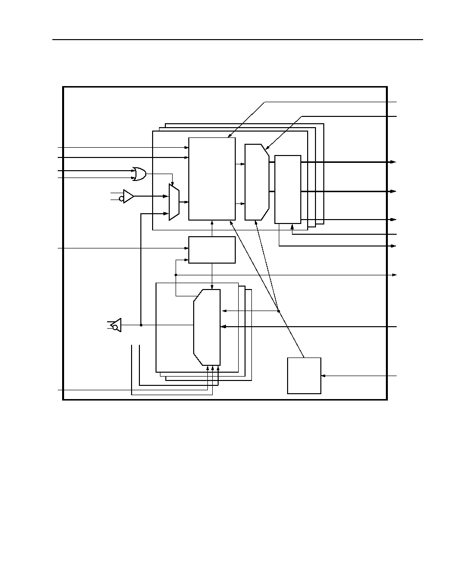
ble edge clocked by the corresponding clock. Figure 1
shows the ORT8850 block diagram.
Backplane Transceiver Interface
The advantage of the ORT8850 FPSC is to bring spe-
cific networking functions to an early market presence
using programmable logic in a system.
The 850 Mbits/s backplane transceiver core allows the
ORT8850 to communicate across a backplane or on a
given board at an aggregate speed of 6.8 Gbits/s, pro-
viding a physical medium for high-speed asynchronous
serial data transfer between system devices. This
device is intended for, but not limited to, connecting ter-
minal equipment in SONET/SDH, ATM, and IP sys-
tems.
The backplane transceiver core is used to support a
6.8 Gbits/s interface for backplane connection to a
mate TADM042G5 device or other SONET devices
such as redundant central crossconnect. The interface
is implemented as an eight-channel 850 Mbits/s LVDS
links. The HSI macrocell is used for clock/data recov-
ery (CDR) and serialize/deserialize between the
106.25 MHz byte-wide internal data buses and the
850 Mbits/s serial LVDS links. For a 622 Mbits/s
SONET stream, the HSI will perform clock and data
recovery (CDR) and MUX/deMUX between 77.76 MHz
byte-wide internal data buses and 622 Mbits/s serial
LVDS links.
Each 850 Mbits/s serial link uses a pseudo-SONET
protocol. SONET A1/A2 framing is used on the link to
detect the 8 kHz frame location. The link is also scram-
bled using the standard SONET scrambler definition to
ensure proper transitions on the link for improved CDR
performance. Selectable transport overhead (TOH)
bytes are insertable in the transmit direction. All the
selectable bytes are inserted from software program-
mable registers that are accessed via a microproces-
sor interface.
Elastic buffers (FIFOs) are used to align each incoming
STS-12 link to the 77.76 MHz clock and 8 kHz frame.
These FIFOs will absorb delay variations between the
four 622 Mbits/s links due to timing skews between
cards and along backplane traces. For greater varia-
tions, a streamlined pointer processor (pointer mover)
within the STM macro will align the 8 kHz frames
regardless of their incoming frame position.
The backplane transceiver allows for SONET scram-
bling and frame alignment or 8-bit/10-bit (8B/10B)
encoding/decoding. SONET has the advantage of
reduced overhead (3.3% overhead for SONET vs. 25%
overhead for 8B/10B). 8B/10B has the advantage of
faster synchronization (a few bytes of transferred data
for 8B/10B vs. up to 500
µ
s for four frames of data for
SONET). The effective data transfer rate for scrambled
SONET is greater than 800 Mbits/s while the effective
data transfer rate for 8B/10B is greater than
680 Mbits/s. Frame synchronization and multichannel
alignment is provided in 8B/10B mode through the use
of special K characters.
Figure 2 shows the architecture of the ORT8850 back-
plane transceiver core.
Agere Systems Inc.
13
Data Sheet
August 2001
Eight-Channel x 850 Mbits/s Backplane Transceiver
ORCA ORT8850 FPSC
ORT8850 Overview
(continued)
1729(F)
Figure 1. ORCA ORT8850 Block Diagram
STANDARD
FPGA
I/Os
ORCA
SERIES 4
FPGA LOGIC
LVDS I/Os
311 MHz
DDR
INTERFACE
8-bit/10-bit
ENCODER
8-bit/10-bit
DECODER
PSEUDO-
SONET
FRAMER
∑
POINTER MOVER
∑
SCRAMBLING
∑
FIFO ALIGNMENT
∑
SELECTED TOH
CLOCK/DATA
RECOVERY
BYTE-
WIDE
DATA
LVDS
850 Mbits/s
DATA
850 Mbits/s
DATA
8 FULL-
SERIAL
DUPLEX
CHANNELS
LVDS I/Os
LVDS I/Os
I/Os
(RapidIO)
311 MHz
DDR
INTERFACE
(RapidIO)
311 MHz
DDR
INTERFACE
(RapidIO)
14
Agere Systems Inc.
Data Sheet
August 2001
Eight-Channel x 850 Mbits/s Backplane Transceiver
ORCA ORT8850 FPSC
ORT8850 Overview
(continued)
Figure 2. High-Level Diagram of ORT8850 Transceiver
IO R IN G
S O F T
C N T L
T X D _A [7 :0]
TX S O C _ A
TXC L K_A
R XD _ A[7:0 ]
R XS O C _A
R X C LK _A
TR A N SM IT
R ST N _ R X_ A
C S YS EN B_A
T X D [31 :0 ]
TXS O C
YTR IS T N _A
U T X T R IST N _ A
R ST N _ U T X_ A
U T X D _A [3 1:0]
U T X SO C _A
PLL
W C D
F P G A
W U TXC LK_FPG A
Z R X D _A [3 1:0]
Z R X SO C _A
Z R X SO C VIO L_ A
Z R X AL N VIO L_ A
Z R X C LK _A
W R X C LK _A _F P G A
PFC L K
STM MACRO + CDR
8
8
T X
R X
8
8
2
1
4
12 X8
8
10
9
1
9X 8
(8 CH ANNELS)
8 D A T A + PAR
8 B/10 B K -C O N T R O L IN P U T S
L IN E _F P, S YS _F P
S YS _C L K
P R O T _ SW
8 D A T A + SP E + C 1 J1 + PAR + EN
8 R E C O VE R ED C LK S
TOH BLOCK
8 D A T A + TO H _ C K_ EN + TO H _ F P
8 D A T A + TO H _ C K_ EN
TO H _C L K
CDR + STM
RapidIO A
U P IN T ER F A C E
PW R U PR S T
F R O M F P G A
(G O E S T O
AL L BL O C KS )
S YS T EM
B U S
F IF O
TR A N SM IT
M O D U L E
R EC E IVE
M O D U L E
S O F T
C N T L
T X D _B [7 :0]
TX S O C _ B
TXC L K_B
R XD _ B[7:0 ]
R XS O C _B
R X C LK _B
TR A N SM IT
R ST N _ R X_ B
C S YS EN B_B
T X D [31 :0 ]
TXS O C
YTR IS T N _B
U T X T R IST N _ B
R ST N _ U T X_ B
U T X D _B [3 1:0]
U T X SO C _B
W C D
W U TXC LK_FPG A
Z R X D _B [3 1:0]
Z R X SO C _B
Z R X SO C VIO L_ B
Z R X AL N VIO L_ B
Z R X C LK _B
W R X C LK _B _F P G A
PFC L K
RapidIO B
F IF O
TR A N SM IT
M O D U L E
R EC E IVE
M O D U L E
S O F T
C N T L
T X D _C [7:0 ]
TX S O C _ C
TXC L K_C
R XD _ C [7 :0]
R XS O C _C
R X C LK _C
TR A N SM IT
R ST N _ R X_ C
C S YS EN B _C
T X D [31 :0 ]
TXS O C
Y T R IST N _ C
U T X TR IS T N _C
R ST N _ U T X _ C
U T XD _ C [31 :0 ]
U T X SO C _C
W C D
W U TXC LK_FPG A
Z R XD _ C [31 :0 ]
Z R X SO C _C
ZR XS O C VIO L _C
ZR XA LN VIO L _C
Z R XC L K_ C
W R X C LK _C _ F PG A
PFC L K
RapidIO C
F IF O
TR A N SM IT
M O D U L E
R EC E IVE
M O D U L E
SO FT
C N T L
8
SO FT
C N T L
8

Agere Systems Inc.
15
Data Sheet
August 2001
Eight-Channel x 850 Mbits/s Backplane Transceiver
ORCA ORT8850 FPSC
ORT8850 Overview
(continued)
HSI Interface
The high-speed interconnect (HSI) macrocell is used
for clock/data recovery and MUX/deMUX between
106.25 MHz byte-wide internal data buses and
850 Mbits/s external serial links.
The HSI interface receives eight 850 Mbits/s serial
input data streams from the LVDS inputs and provides
eight independent 106.25 MHz byte-wide data streams
and recovered clock to the STM macro. There is no
requirement for bit alignment since SONET type fram-
ing will take place inside the ORT850 core. For trans-
mit, the HSI converts four byte-wide 106.25 MHz data
streams to serial streams at 850 Mbits/s at the LVDS
outputs.
STM Macrocell
The STM portion of the embedded core consists of
transmitter (Tx) and receiver (Rx) sections. The
receiver receives eight byte-wide data streams at
106.25 MHz and the associated clocks from the HSI. In
the Rx section, the incoming streams are SONET
framed and descrambled before they are written into a
FIFO, which absorbs phase and delay variations and
allows the shift to the system clock. The TOH is then
extracted and sent out on the eight serial ports. The
pointer mover consists of three blocks: pointer inter-
preter, elastic store, and pointer generator. The pointer
interpreter finds the synchronous transport signal
(STS) synchronous payload envelopes (SPE) and
places it into a small elastic store from which the
pointer generator will produce eight byte-wide STS-12
streams of data that are aligned to the system timing
pulse.
In the Tx section, transmitted data for each channel is
received through a parallel bus and a serial port from
the FPGA circuit. TOH bytes are received from the
serial input port and can be optionally inserted from
programmable registers or serial inputs to the STS-12
frame via the TOH processor. Each of the eight parallel
input buses is synchronized to a free-running system
clock. Then the SPE and TOH data is transferred to the
HSI.
The STM macrocell also has a scrambler/descrambler
disable feature, allowing the user to disable the scram-
bler of the transmitter and the descrambler of the
receiver. Also, unused channels can be disabled to
reduce power dissipation.
8B/10B Encoder/Decoder
The ORT8850 facilitates high-speed serial transfer of
data in a variety of applications including Gigabit Ether-
net, fibre channel, serial backplanes, and proprietary
links. The device provides 8B/10B coding/decoding for
each channel. The 8B/10B transmission code includes
serial encoding/decoding rules, special characters, and
error detection.
Information to be transmitted over a fibre shall be
encoded eight bits at a time into a 10-bit transmission
character and then sent serially. The 10-bit transmis-
sion characters support all 256 eight-bit combinations.
Some of the remaining transmission characters
referred to as special characters, are used for functions
which are to be distinguishable from the contents of a
frame.
FPGA Interface
The FPGA logic will receive/transmit frame-aligned
(optional for 8B/10B mode) streams of 106.25 MHz
data (maximum of eight streams in each direction)
from/to the backplane transceiver embedded core. All
frames transmitted to the FPGA will be aligned to the
FPGA frame pulse which will be provided by the FPGA
user's logic to the STM macro. If the receive pointer
mover and alignment FIFOs are bypassed, then each
channel will provide its own receive clock and receive
frame pulse signals. Otherwise, all frames received
from the FPGA logic will be aligned to the system
frame pulse that will be supplied to the STM macro
from the FPGA user's logic.
Byte-Wide Parallel Interface
Three byte-wide parallel interface are provided on the
ORT8850. Each interface provides for transmit and
receive of byte-wide data, one control signal, and one
clock. Receive data is sampled on both edges of the
receive clock and is converted to a 32-bit data bus,
which is single-edge clocked by a half-speed clock for
transfer to the FPGA logic. Maximum transmit/receive
clock rate is 311 MHz and 155 MHz for the internal
FPGA clock. This allows for a 622 Mbits/s link data
transfer rate. Other functions provided include a check
for a minimum number of transferred bytes.
The first byte-wide interface (RapidIO A in Figure 2) is
always available. The other two interfaces (RapidIO B
and RapidIO C) are available when the 850 Mbits/s
serial links are not being used.

16
16
Agere Systems Inc.
Data Sheet
August 2001
Eight-Channel x 850 Mbits/s Backplane Transceiver
ORCA ORT8850 FPSC
ORT8850 Overview
(continued)
FPSC Configuration
Configuration of the ORT8850 occurs in two stages:
FPGA bit stream configuration and embedded core
setup.
FPGA Configuration
Prior to becoming operational, the FPGA goes through
a sequence of states, including powerup, initialization,
configuration, start-up, and operation. The FPGA logic
is configured by standard FPGA bit stream configura-
tion means as discussed in the Series 4 FPGA data
sheet. The options for the embedded core are set via
registers that are accessed through the FPGA system
bus. The system bus can be driven by an external PPC
compliant microprocessor via the MPI block or via a
user master interface in FPGA logic. A simple IP block,
that drives the system by using the user interface and
uses very little FPGA logic, is available in the MPI/Sys-
tem Bus application note (AP01-032NCIP). This IP
block sets up the embedded core via a state machine
and allows the ORT8850 to work in an independent
system without an external microprocessor interface.
Embedded Core Setup
All options for the operation of the core are configured
according to the device register map, which is included
with the ORT8850 FPSC simulation kit.
During the powerup sequence, the ORT8850 device
(FPGA programmable circuit and the core) is held in
reset. All the LVDS output buffers and other output
buffers are held in 3-state. All flip-flops in the core area
are in reset state, with the exception of the boundry-
scan shift registers, which can only be reset by bound-
ary-scan reset. After powerup reset, the FPGA can
start configuration. During FPGA configuration, the
ORT8850 core will be held in reset and all the local bus
interface signals forced high, but the following active-
high signals (PROT_SWITCH_A, PROT_SWITCH_C,
TX_TOH_CK_EN, SYS_FP, LINE_FP) will be forced
low. The CORE_READY signal sent from the embed-
ded core to FPGA is held low, indicating that the core is
not ready to interact with FPGA logic. At the end of the
FPGA configuration sequence, the CORE_READY sig-
nal will be held low for six SYS_CLK cycles after
DONE, TRI_IO and RST_N (core global reset) are
high. Then it will go active-high, indicating the embed-
ded core is ready to function and interact with FPGA
programmable circuit. During FPGA reconfiguration
when DONE and TRI_IO are low, the CORE_READY
signal sent from the core to FPGA will be held low
again to indicate the embedded core is not ready to
interact with FPGA logic. During FPGA partial configu-
ration, CORE_READY stays active. The same FPGA
configuration sequence described previously will
repeat again.
The initialization of the embedded core consists of two
steps: register configuration and synchronization of the
alignment FIFO. In order to configure the embedded
core, the registers need to be unlocked by writing
0x30005 to address 0x30004 and writing 0x80 to
address 0x05. Control registers 0x30004 and 0x30005
are lock registers. If the output bus of the data, serial
TOH port, and TOH clock and TOH frame pulse are
controlled by 3-state registers (the use of the registers
for 3-state output control is optional; these output 3-
state enable signals are brought across the local bus
interface and available to the FPGA side), the next step
is to activate the 3-state output bus and signals by tak-
ing them to functional state from high-impedance state.
This can be done by writing 0x01 to correspond bits of
the channel registers 0x30020, 0x30038, 0x30050,
0x30068, 0x30080, 0x30090, 0x300B0, and 0x300C8.
In addition, the synchronization of selected streams is
recommended for some networking systems applica-
tions. This requires a resync of the alignment FIFO
after the enabled channels have a valid frame pulse or
8B/10B control character. See the sections about STM
Link Alignment Setup or 8B/10B Link Alignment Setup
for more details.

Agere Systems Inc.
17
Data Sheet
August 2001
Eight-Channel x 850 Mbits/s Backplane Transceiver
ORCA ORT8850 FPSC
Generic Backplane Transceiver
Application
Synchronous Transfer Mode (STM)
The combination of ORT8850 and soft IP cores pro-
vides a generic data moving solution for non-SONET
applications. There is no requirement for SONET
knowledge to the users. All that is needed is to supply
the pseudo-SONET framer with data, clock, and a
8 kHz frame pulse. The provision registers may also
need to be set up, and this can be done through either
the FPGA MPI, or in a state machine in the FPGA sec-
tion (VHDL code available from Agere).
The 8 kHz frame pulse must be supplied to the
SYS_FP signal. For generic applications, the frame
pulse can be created in FPGA logic from the
77.76 MHz SYS_CLK using a simple resettable
counter (the frame pulse should only be high for one
cycle of the SYS_CLK). A VHDL core that automati-
cally provides the 8 kHz frame pulse is available from
Agere. Byte-wide data is then sent to each of the trans-
mit channels as follows: the first 36 bytes transferred
will be invalid data (replaced by overhead), where the
first byte is sent on the rising edge of SYS_CLK when
SYS_FP is high. The next 1044 byte positions can be
filled with valid data. This will repeat a total of nine
times (36 invalid bytes followed by
1044 valid bytes) at which time the next 8 kHz frame
pulse will be found. Thus, 87 out of 90 (96.7%) of the
data bytes sent are valid user data. The ORT8850 also
supports a transparent mode where only the first
24 bytes are invalid data (A1/A2 frame bytes) followed
by 9,684 bytes of valid user data.
On the receive side, an 8 kHz pulse must again be sup-
plied to LINE_FP. In this case, however, only the signal
DOUT<channel>_SPE (where the eight channels are
labeled AA, AB, AC, AD, BA, BB, BC, and BD) must be
monitored for each channel, where a high value on this
signal means valid data. Again, 87 out 90 bytes
received (96.7%) will be valid data. Transparent mode
is also supported for receive data.
8B/10B Mode
The ORT8850 facilitates high-speed serial transfer of
data in a variety of applications including Gigabit
Ethernet, fibre channel, serial backplanes, and
proprietary links. In place of the STM interface, the
ORT8850 also provides 8B/10B coding/decoding for
each channel. The 8B/10B transmission code includes
serial encoding/decoding rules, special characters, and
error detection. In 8B/10B mode, LSB is received first
and transmitted first. The 10-bit encoded transmission
characters labeled as a, b, c, d, e, i, f, g, h, and j are
transmitted with bit a first and bit j last, where bit a is
the LSB and bit j is the MSB.
Transmitter Description
The data input to the transmitter of each channel is an
8-bit word and a K-control input. The K input is used to
identify data or a special character. For each channel,
the input data byte is clocked into a FIFO. When K-con-
trol is 1, the data on the parallel input is mapped into its
corresponding control character. The transmit FIFOs
must be initialized upon the deassertion of the RST_N
signal.
Receiver Description
Clock recovery is performed by the HSI on the input
data stream for each channel of the ORT8850. The
recovered data is then aligned to the 10-bit word
boundary. Word alignment is accomplished by detect-
ing and aligning to the 8B/10B comma sequence. The
HSI will detect and align to either polarity of the comma
sequence. The 10-bit word aligned data is then
decoded and the 8-bit output is passed to the align-
ment FIFOs. Each receive channel provides a FIFO in
order to adjust for the skew between the channels and
ensure that the first valid data following the comma
character is transmitted simultaneously from all the
channels that are programmed to be aligned.
In the RESET state, each channel is actively searching
for the occurence of a comma character. Once the
channel is powered up, the comma detect pulse will be
found on the doutxx-fp per channel in the FPGA.
Receive Channel Sync Block
In order to account for skews between the channels, it
is necessary to align multiple channels on the comma
character boundary. The sync algorithm assumes that
either all eight channels, two groups of four channels,
or four groups of two channels will be aligned. The
ORT8850 powers up in the RESET state in which no
channel alignment is done.
18
Agere Systems Inc.
Data Sheet
August 2001
Eight-Channel x 850 Mbits/s Backplane Transceiver
ORCA ORT8850 FPSC
Generic Backplane Transceiver Application
(continued)
1757(F)
Figure 3. 8850 with 8B/10B Coding/Decoding
CLOCK
RECOVERY
RX LVDS
TX LVDS
DATA
CLOCK
10
LCKRX
DE
SERI
A
L
I
Z
E
R
A
ND B
Y
T
E
A
L
IGN
RECEIVER CHANNEL (1 OF 8)
10b/8b
DECODER
ALIGNMENT
FIFO
PARALLEL DATA OUT
SYS_CLK
COMMA _DET
DOUTXX_FP
ERROR FLAG
PARALLEL
DATAIN
FIFO
8
10
TRANSMIT CHANNEL (1 OF 8)
8B/10B
ENCODER
S
E
RI
AL
I
Z
ER
DOUTXX
DINXX
Backplane Transceiver Core Detailed
Description
HSI Macro
The 850 high-speed interface (HSI) provides a physical
medium for high-speed asynchronous serial data trans-
fer between ASIC devices. The devices can be
mounted on the same PC board or mounted on differ-
ent boards and connected through the shelf back-
plane. The 850 CDR macro is an eight-channel clock-
phase select (CPS) and data retime function with
serial-to-parallel demultiplexing for the incoming data
stream and parallel-to-serial multiplexing for outgoing
data. The macrocell can be used as a eight-channel or
16-channel configuration. The ORT8850 uses an eight-
channel HSI macro cell. The HSI macro consists of
three functionally independent blocks: receiver, trans-
mitter, and PLL synthesizer as shown in Figure 4.
The PLL synthesizer block generates the necessary
850 MHz clock for operation from a 212 MHz,
106 MHz, or 85 MHz reference. The PLL synthesizer
block is a common asset shared by all eight receive
and transmit channels. The PLL reference clock must
match the interface frequency.
The HSI_RX block receives a differential 850 Mbits/s
(or subrates 424 Mbits/s, 212 Mbits/s) serial data with-
out clock at its LVDS receiver input. Based on data
transitions, the receiver selects an appropriate
850 MHz clock phase for each channel to retime the
data. The retimed data and clock are then passed to
the deMUX (deserializer) module. DeMUX module per-
forms serial-to-parallel conversion and provides three
possible parallel rates, 212 Mbits/s, 106 Mbits/s, or
85 Mbits/s, where the 106 Mbits/s data is used in
SONET mode and the 85 Mbits/s data is used in
8B/10B mode (212 Mbits/s is unused).
The HSI_TX block receives 106 Mbits/s (SONET
mode), or 85 Mbits/s (8B/10B mode) parallel data at its
input. MUX (serializer) module performs a parallel-to-
serial conversion using an 850 MHz clock provided by
the PLL/synthesizer block. The resulting 850 Mbits/s
serial data stream is then transmitted through the
LVDS driver.
The loopback feature built into the HSI macro provides
looping of the transmitter data output into the receiver
input when desired.
All rate examples described here are the maximum
rates possible. The actual HSI internal clock rate is
determined by the provided reference clock rate. For
example, if a 78 MHz reference clock is provided, the
HSI macro will operate at 622 Mbits/s.
Agere Systems Inc.
19
Data Sheet
August 2001
Eight-Channel x 850 Mbits/s Backplane Transceiver
ORCA ORT8850 FPSC
Backplane Transceiver Core Detailed Description
(continued)
5-8592(F).b
Figure 4. HSI Functional Block Diagram
Rx
CDR
SERI
A
L
T
O
PA
R
R
A
L
L
E
L
DEM
U
X
SEL
ECT
848 MHz
CLOCK/DATA
ALIGNMENT
SYNTHESIZER
PLL
LOOPBKCH[(n ≠ 1):0]
LD[(n ≠ 1):0]RX[9:0]
TSTCLK
CREG BYPASS
CREG LOOPBKEN
DIN[(n ≠ 1):0]
848 Mbits/s
SYSCLK
106 MHz
DOUT[(n ≠1):0]
(TEST)
LCKRX[(n ≠ 1):0]
TS
TC
L
K
BY
PASS
(TEST)
RXPWRDN[(n ≠ 1):0]
LCKPLL
106 Mbits/s
LD[(n ≠ 1):0] TX[9:0]
1
2
n
Tx
1
2
n
RETIME
or 85 MHz
or 424 Mbits/s
or 212 Mbits/s DATA
or 85 Mbits/s
PARRAL
L
E
L
T
O
SERI
A
L
MU
X
WORD
ALIGN
TEN
BIT
RC[1:0]CK[(n≠1):0]
ENCOMMA[(n≠1):0]
COMMADET[(n≠1):0]
MODE
CONTROL
EN10BIT
(850 MHz)
RESETTX
RESETRX
848 Mbits/s
or 424 Mbits/s
or 212 Mbits/s DATA
106 Mbits/s
or 85 Mbits/s
106 MHz
or 85 MHz
106 Mbits/s
or 85 Mbits/s
TO
ASIC
BLOCK
20
20
Agere Systems Inc.
Data Sheet
August 2001
Eight-Channel x 850 Mbits/s Backplane Transceiver
ORCA ORT8850 FPSC
Backplane Transceiver Core Detailed
Description
(continued)
STM Transmitter (FPGA
Backplane)
The synchronous transport module (STM) portion of
the embedded core consists of two slices: STM A and
B.
Each STM slice has four STS-12 transmit channels,
which can be treated as a single STS-48 channel. In
general, the transmitter circuit receives four byte-wide
77.76 MHz data from the FPGA, which nominally rep-
resents four STS-12 streams (A, B, C, and D). This
data is synchronized to the system (reference) clock,
and an 8 kHz
system frame pulse from the FPGA logic.
Transport overhead bytes are then optionally inserted
into these streams, and the streams are forwarded to
the HSI. All byte timing pulses required to isolate indi-
vidual overhead bytes (e.g., A1, A2, B1, D1--D3, etc.)
are generated internally based on the system frame
pulse (SYS_FP) received from the FPGA logic. All
streams operate byte-wide at 77.76 MHz in all modes.
The TOH processor operates from 25 MHz to
77.76 MHz and supports the following TOH signals: A1
and A2 insertion and optional corruption; H1, H2, and
H3 pass transparently; BIP-8 parity calculation (after
scrambling) and B1 byte insertion and optional corrup-
tion (before scrambling); optional K1 and K2 insert;
optional S1/M0 insert; optional E1/F1/E2 insert;
optional section data communication channel (DCC,
D1--D3) and line data communication channel (DCC,
D4--D12) insertion (for intercard communications
channel); scrambling of outgoing data stream with
optional scrambler disabling; and optional stream dis-
abling. All streams operate byte-wide at 77.76 MHz
(622 Mbits/s) or 106.25 MHz (850 Mbits/s) in all modes.
When the ORT8850 is used in nonnetworking applica-
tions as a generic high-speed backplane data mover,
the TOH serial ports are unused or can be used for
slow-speed, off-channel communication between
devices. An optional transparent mode is available
where only the twelve A1 and twelve A2 bytes are used
for frame alignment and synchronization.
Data received on the parallel bus is optionally scram-
bled and transferred to LVDS outputs.
Byte Ordering Information
The STM macro slice (i.e., A, B) supports quad STS-
12, quad STS-3, and quad STS-1 modes of operation
on the input/output ports. STS-48 is also supported, but
it must be received in the quad STS-12 format. When
operating in quad STS-12 mode, each of the indepen-
dent byte streams carries an entire STS-12 within it.
Figure 5 reveals the byte ordering of the individual
STS-12 streams and for STS-48 operation. Note that
the recovered data will always continue to be in the
same order as transmitted.
5-8574 (F)
Figure 5. Byte Ordering of Input/Output Interface in STS-12 Mode
12
24
36
48
9
21
33
45
6
18
30
42
3
15
27
39
11
23
35
47
8
20
32
44
5
17
29
41
2
14
26
38
10
22
34
46
7
19
31
43
4
16
28
40
1
13
25
37
1, 12
2, 12
3, 12
4, 12
1, 9
2, 9
3, 9
4, 9
1, 6
2, 6
3, 6
4, 6
1, 3
2, 3
3, 3
4, 3
1, 11
2, 11
3, 11
4, 11
1, 8
2, 8
3, 8
4, 8
1, 5
2, 5
3, 5
4, 5
1, 2
2, 2
3, 2
4, 2
1, 10
2, 10
3, 10
4, 10
1, 7
2, 7
3, 7
4, 7
1, 4
2, 4
3, 4
4, 4
1, 1
2, 1
3, 1
4, 1
STS-12 A
STS-12 B
STS-12 C
STS-12 D
STS-12 A
STS-12 B
STS-12 C
STS-12 D
STS-48 IN QUAD STS-12 FORMAT
QUAD STS-12

Agere Systems Inc.
21
Data Sheet
August 2001
Eight-Channel x 850 Mbits/s Backplane Transceiver
ORCA ORT8850 FPSC
Backplane Transceiver Core Detailed
Description
(continued)
Transport Overhead for In-Band Communication
The TOH byte can be used for in-band configuration,
service, and management since it is carried along the
same channel as data. In ORT8850, in-band signaling
can be efficiently utilized, since the total cost of over-
head is only 3.3%.
Transport Overhead Insertion (Serial Link)
The TOH serial links are used to insert TOH bytes into
the transmit data. The transmit TOH data and
TOH_CLK_EN get retimed by TOH_CLK in order to
meet setup and hold specifications of the device.
The retimed TOH data is shifted into a 288-bit (36-byte
by 8-bit) shift register and then multiplexed as an 8-bit
bus to be inserted into the byte-wide data stream.
Insertion from these serial links or pass-through of
TOH from the byte-wide data is under software control.
Transport Overhead Byte Ordering
(FPGA to Backplane)
In the transparent mode, SPE and TOH data received
on parallel input bus is transferred, unaltered, to the
serial LVDS output. However, B1 byte of STS#1 is
always replaced with a new calculated value (the
11 bytes following B1 are replaced with all zeros). Also,
A1 and A2 bytes of all STS-1s are always regenerated.
TOH serial port in not used in the transparent mode of
operation.
In the TOH insert mode, SPE bytes are transferred,
unaltered, from the input parallel bus to the serial LVDS
output. On the other hand, TOH bytes are received
from the serial input port and are inserted in the STS-
12 frame before being sent to the LVDS output.
Although all TOH bytes from the 12 STS-1s are trans-
ferred into the device from each serial port, not all of
them get inserted in the frame. There are three hard-
coded exceptions to the TOH byte insertion:
s
Framing bytes (A1/A2 of all STS-1s) are not inserted
from the serial input bus. Instead, they can always be
regenerated.
s
Parity byte (B1 of STS#1) is not inserted from the
serial input bus. Instead, it is always recalculated
(the 11 bytes following B1 are replaced with all
zeros).
s
Pointer bytes (H1/H2/H3 of all STS-1s) are not
inserted from the serial input bus. Instead, they
always flow transparently from parallel input to LVDS
output.
In addition to the above hardcoded exceptions, the
source of some TOH bytes can be further controlled by
software. When configured to be in pass-through
mode, the specific bytes must flow transparently from
the parallel input. Note that blocks of 12 STS-1 bytes
forming an STS-12 are controlled as a whole. There
are 15 software controls per channel, as listed below:
s
Source of K1 and K2 bytes of the 12 STS-1s
(24 bytes) is specified by a control bit (per channel
control).
s
Source of S1 and M0 bytes of the 12 STS-1s
(24 bytes) is specified by a control bit (per channel
control).
s
Source of E1, F1, E2 bytes of the STS-1s (36 bytes)
is specified by a control it (per channel control).
s
Source of D1 bytes of the STS-1s (12 bytes) is spec-
ified by a control bit (per channel control).
s
Source of D2 bytes of the 12 STS-1s (12 bytes) is
specified by a control bit (per channel control).
s
Source of D3 bytes of the 12 STS-1s (12 bytes) is
specified by a control bit (per channel control).
s
Source of D4 bytes of the 12 STS-1s (12 bytes) is
specified by a control bit (per channel control).
s
Source of D5 bytes of the 12 STS-1s (12 bytes) is
specified by a control bit (per channel control).
s
Source of D6 bytes of the 12 STS-1s (12 bytes) is
specified by a control bit (per channel control).
s
Source of D7 bytes of the 12 STS-1s (12 bytes) is
specified by a control bit (per channel control).
s
Source of D8 bytes of the 12 STS-1s (12 bytes) is
specified by a control bit (per channel control).
s
Source of D9 bytes of the 12 STS-1s (12 bytes) is
specified by a control bit (per channel control).
s
Source of D10 bytes of the 12 STS-1s (12 bytes) is
specified by a control bit (per channel control).
s
Source of D11 bytes of the 12 STS-1s (12 bytes) is
specified by a control bit (per channel control).
s
Source of D12 bytes of the 12 STS-1s (12 bytes) is
specified by a control bit (per channel control).
TOH reconstruction is dependent on the transmitter
mode of operation. In the transparent mode, TOH
bytes on LVDS output are as shown in Table 2.
A new capability in the ORT8850 allows the user to
choose not to insert the B1 byte and the following
11 bytes of zeros. This option is also available for the
A1 and A2 bytes.
22
Agere Systems Inc.
Data Sheet
August 2001
Eight-Channel x 850 Mbits/s Backplane Transceiver
ORCA ORT8850 FPSC
Backplane Transceiver Core Detailed Description
(continued)
Table 2. Transmitter TOH on LVDS Output (Transparent Mode)
In the TOH insert mode of operation, TOH bytes on LVDS output are shown in Table 3. This also shows the order
in which data is transferred to the serial TOH interface, starting with the most significant bit of the first A1 byte. The
first bit of the first byte is replaced by an even parity check bit over all TOH bytes from the previous TOH frame.
Table 3. Transmitter TOH on LVDS Output (TOH Insert Mode)
A1/A2 Frame Insert and Testing
The A1 and A2 bytes provide a special framing pattern that indicates where a STS-1 begins in a bit stream. All
12 A1 bytes of each STS-12 are set to 0xF6, and all 12 A2 bytes of the STS-12 are set to 0x28 when not overrid-
den with an user-specified value for testing. The latency from the transmission of the first bit of the A1 byte at the
device output pins from the transmit frame pulse (SYS_FP) at the FPGA to embedded core input is between five to
seven cycles of fpga_sysclk.
A1/A2 testing (corruption) is controlled per stream by the A1/A2 error insert register. When A1/A2 corruption detec-
tion is set for a particular stream, the A1/A2 values in the corrupted A1/A2 value registers are sent for the number
of frames defined in the corrupted A1/A2 frame count register. When the corrupted A1/A2 frame count register is
set to zero, A1/A2 corruption will continue until the A1/A2 error insert register is cleared. This also allows alternate
values to be set for A1 and A2 during normal operation. For the ORT8850, it is optionally possible to not insert A1
and A2.
On a per-device basis, the A1 and A2 byte values are set, as well as the number of frames of corruption. Then, to
insert the specified A1/A2 values, each channel has an enable register. When the enable register is set, the A1/A2
values are corrupted for the number specified in the number of frames to corrupt. To insert errors again, the per-
channel fault insert register must be cleared, and set again. Only the last A1 and the first A2 are corrupted.
A1
A1
A1
A1
A1
A1
A1
A1
A1
A1
A1
A1
A2
A2
A2
A2
A2
A2
A2
A2
A2
A2
A2
A2
B1
0
0
0
0
0
0
0
0
0
0
0
Regenerated bytes.
Transparent bytes from parallel input port.
A1
A1
A1
A1
A1
A1
A1
A1
A1
A1
A1
A1
A2
A2
A2
A2
A2
A2
A2
A2
A2
A2
A2
A2
B1
0
0
0
0
0
0
0
0
0
0
0
E1
E1
E1
E1
E1
E1
E1
E1
E1
E1
E1
E1
F1
F1
F1
F1
F1
F1
F1
F1
F1
F1
F1
F1
D1
D1
D1
D1
D1
D1
D1
D1
D1
D1
D1
D1
D2
D2
D2
D2
D2
D2
D2
D2
D2
D2
D2
D2
D3
D3
D3
D3
D3
D3
D3
D3
D3
D3
D3
D3
H1
H1
H1
H1
H1
H1
H1
H1
H1
H1
H1
H1
H2
H2
H2
H2
H2
H2
H2
H2
H2
H2
H2
H2
H3
H3
H3
H3
H3
H3
H3
H3
H3
H3
H3
H3
K1
K1
K1
K1
K1
K1
K1
K1
K1
K1
K1
K1
K2
K2
K2
K2
K2
K2
K2
K2
K2
K2
K2
K2
D4
D4
D4
D4
D4
D4
D4
D4
D4
D4
D4
D4
D5
D5
D5
D5
D5
D5
D5
D5
D5
D5
D5
D5
D6
D6
D6
D6
D6
D6
D6
D6
D6
D6
D6
D6
D7
D7
D7
D7
D7
D7
D7
D7
D7
D7
D7
D7
D8
D8
D8
D8
D8
D8
D8
D8
D8
D8
D8
D8
D9
D9
D9
D9
D9
D9
D9
D9
D9
D9
D9
D9
D10
D10
D10
D10
D10
D10
D10
D10
D10
D10
D10
D10
D11
D11
D11
D11
D11
D11
D11
D11
D11
D11
D11
D11
D12
D12
D12
D12
D12
D12
D12
D12
D12
D12
D12
D12
S1
S1
S1
S1
S1
S1
S1
S1
S1
S1
S1
S1
M0
M0
M0
M0
M0
M0
M0
M0
M0
M0
M0
M0
E2
E2
E2
E2
E2
E2
E2
E2
E2
E2
E2
E2
Regenerated bytes.
Inserted or transparent bytes. Blocks of 12 STS-1 bytes are controlled as a whole. There are 15 controls/channel: K1/K2, S1/M0, E1/F1/E2, D1, D2, D3, D4, D5, D6, D7, D8, D9, D10,
D11, D12.
Transparent bytes (from parallel input port).
Inserted bytes from TOH serial input port.

Agere Systems Inc.
23
Data Sheet
August 2001
Eight-Channel x 850 Mbits/s Backplane Transceiver
ORCA ORT8850 FPSC
Backplane Transceiver Core Detailed
Description
(continued)
B1 Calculation and Insertion
In a bit interleaved parity -8 (BIP-8) error check set for
even parity over all the bits of an STS-1 frame B1 is
defined for the first STS-1 in an STS-N only, the B1 cal-
culation block computes a BIP-8 code, using even par-
ity over all bits of the previous STS-12 frame after
scrambling and is inserted in the B1 byte of the current
STS-12 frame before scrambling. Per-bit B1 corruption
is controlled by the force BIP-8 corruption register (reg-
ister address 0F). For any bit set in this register, the
corresponding bit in the calculated BIP-8 is inverted
before insertion into the B1 byte position. Each stream
has an independent fault insert register that enables
the inversion of the B1 bytes. B1 bytes in all other STS-
1s in the stream are filled with zeros. For the ORT8850,
it is optionally possible to not insert B1 and the subse-
quent 11 bytes of zeros.
Stream Disable
When disabled via the appropriate bit in the stream
enable register, the prescrambled data for a stream is
set to all ones, feeding the HSI. The HSI macro is pow-
ered down on a per-stream basis, as are its LVDS out-
puts.
Scrambler
The data stream is scrambled using a frame-synchro-
nous scrambler with a sequence length of 127. The
scrambling function can be disabled by software. The
generating polynomial for the scrambler is 1 + x
6
+ x
7
.
This polynomial conforms to the standard SONET
STS-12 data format. The scrambler is reset to 1111111
on the first byte of the SPE (byte following the Z0 byte
in the twelfth STS-1). That byte and all subsequent
bytes to be scrambled are exclusive-ORed, with the
output from the byte-wise scrambler. The scrambler
runs continuously from that byte on throughout the
remainder of the frame. A1, A2, J0, and Z0 bytes are
not scrambled.
System Frame Pulse and Line Frame Pulse
System frame pulse (for transmitter) and line frame
pulse (for receiver) are generated in FPGA logic. A1/A2
framing is used on the link for locating the 8 kHz frame
location. All frames sent to the FPGA are aligned to the
FPGA frame pulse LINE_FP which is provided by the
FPGA to the STM macro. All frames sent from the
FPGA to the STM will be aligned to the frame pulse
SYS_FP that is supplied to the STM macro. In either
direction, the system frame pulse and line frame pulse
are active for one system clock cycle, indicating the
location of A1 byte of STS#1. They are common to all
eight channels except when the pointer mover and
alignment FIFOs are bypassed. In that case, a line
frame pulse for each receive channel is generated by
the STM macro and passed to the FPGA interface.
Repeater
This block is essentially the inverse of the sampler
block. It receives byte-wide STS-12 rate data from the
TOH insert block. In order to support the quad STS-1
and STS-3 modes of operation, the HSI (622 Mbits/s)
can be connected to a slower speed device (e.g.,
155 Mbits/s or 52 Mbits/s). The purpose of this block is
to rearrange the data being fed to the HSI so that each
bit is transmitted four or twelve times, thus simulating
155 Mbits/s or 51.84 Mbits/s serial data. For example,
in STS-3 mode, the incoming STS-12 stream is com-
posed of four identical STS-3s so only every fourth
byte is used. The bit expansion process takes a single
byte and stretches it to take up 4 bytes each consisting
of
4 copies of the 8 bits from the original byte. In STS-1
mode, every twelfth byte is used and four groups of
3 bytes of the form AAAAAAAA, AAAABBBB, and
BBBBBBBB are forwarded to the HSI. An alternate
method for supplying STS-1 mode is to set the HSI to
run at 207.36 MHz and use the four times repeater
function.
STM Receiver (Backplane
FPGA)
Each of the two STM slices of the ORT8850 has four
receiving channels that can be treated as one STS-48
stream, or treated as independent channels. Incoming
data is received through LVDS serial ports at the data
rate of 622 Mbits/s. The receiver can handle the data
streams with frame offsets of up to ±12 bytes which
would be due to timing skews between cards and along
backplane traces or other transmission medium. In
order for this multichannel alignment capability to oper-
ate properly, it should be noted that while the skew
between channels can be very large, they must oper-
ate at the exact same frequency (0 ppm frequency
deviation), thus requiring that their transmitters be
driven by the same clock source. The received data
streams are processed in the HSI and the STM, and
then passed through the CIC boundary to the FPGA
logic.

24
24
Agere Systems Inc.
Data Sheet
August 2001
Eight-Channel x 850 Mbits/s Backplane Transceiver
ORCA ORT8850 FPSC
Backplane Transceiver Core Detailed
Description
(continued)
Framer Block
The framer block takes byte-wide data from the HSI,
and outputs a byte-aligned, byte-wide data stream and
8 kHz sync pulse. The framer algorithm determines the
out-of-frame/in-frame status of the incoming data and
will cause interrupts on both an errored frame and an
out-of-frame (OOF) state. The framer detects the A1/
A2 framing pattern and generates the 8 kHz frame
pulse. When the framer detects OOF, it will generate
an interrupt. Also, the framer detects an errored frame
and increments an A1/A2 frame error counter. The
counter can be monitored by a processor to compile
performance status on the quality of the backplane.
Because the ORT8850 is intended for use between it
and another ORT8850 or other devices via a back-
plane, there is only one errored frame state. Thus, after
two transitions are missed, the state machine goes into
the OOF state and there is no severely errored frame
(SEF) or loss-of-frame (LOF) indication.
B1 Calculate
Each Rx block receives byte-wide scrambled
77.76 MHz data and a frame sync from the framer.
Since each HSI is independently clocked, the Rx block
operates on individual streams. Timing signals required
to locate overhead bytes to be extracted are generated
internally based on the frame sync. The Rx block pro-
duces byte-wide (optionally) descrambled data and an
output frame sync for the alignment FIFO block. The
frame sync signals are also sent to the FPGA logic for
use when the alignment FIFO block is bypassed.
The B1 calculation block computes a BIP-8 (bit inter-
leaved parity 8 bits) code, using even parity over all bits
of the previous STS-12 frame before descrambling;
this value is checked against the B1 byte of the current
frame after descrambling. A per-stream B1 error
counter is incremented for each bit that is in error. The
error counter may be read via the CPU interface.
Descrambling. The streams are descrambled using a
frame synchronous descrambler with a sequence
length of 127 with a generating polynomial of 1 + x
6
+
x
7
. The A1/A2 framing bytes, the section trace byte
(J0) and the growth bytes (Z0) are not descrambled.
The descrambling function can be disabled by soft-
ware.
Sampler. This block operates on the byte-wide data
directly from the HSI macro. The HSI external interface
always runs at 622 Mbits/s (STS-12), or 850 Mbits/s,
but it can be connected directly to a 155 Mbits/s STS-3
stream or a 51.84 Mbits/s STS-1 stream. If connected
to either a 155 Mbits/s or 51.84 Mbits/s stream, each
incoming data is received either 4 or 12 times respec-
tively. This block is used to return the byte stream to
the expected STS-12 format. The mode of operation is
controlled by a register and can either be STS-12
(pass-through), STS-3 (every fourth bit), or STS-1
(every twelfth bit). The output from this block is not bit-
aligned (i.e., an 8-bit sample does not necessarily con-
tain an entire SONET byte), but it is in standard
SONET STS-12 format (i.e., four STS-3s or 12 STS-
1s) and is suitable for framing.
AIS-L Insertion. Alarm indication signal (AIS) is a con-
tinuous stream of unframed 1s sent to alert down-
stream equipment that the near-end terminal has
failed, lost its signal source, or has been temporarily
taken out of service. If enabled in the AIS_L force reg-
ister, AIS-L is inserted into the received frame by writ-
ing all ones for all bytes of the descrambled stream.
AIS-L Insertion on Out-of-Frame. If enabled via a
register, AIS-L is inserted into the received frame by
writing all ones for all bytes of the descrambled stream
when the framer indicates that an out-of-frame condi-
tion exists.
Internal Parity Generation
Even parity is generated on all data bytes and is routed
in parallel with the data to be checked before the pro-
tection switch MUX at the parallel output.
Agere Systems Inc.
25
Data Sheet
August 2001
Eight-Channel x 850 Mbits/s Backplane Transceiver
ORCA ORT8850 FPSC
Backplane Transceiver Core Detailed Description
(continued)
Transport Overhead Extraction
Transport overhead is extracted from the receive data stream by the TOH extract block. The incoming data gets
loaded into a 36-byte shift register on the system clock domain. This, in turn, is clocked onto the TOH clock domain
at the start of the SPE time, where it can be clocked out.
During the SPE time, the receiver TOH frame pulse is generated, RX_TOH_FP, which indicates the start of the row
of 36 TOH bytes. This pulse, along with the receive TOH clock enable, RX_TOH_CK_EN, as well as the TOH data,
are all launched on the rising edge of the TOH clock TOH_CLK.
TOH Byte Ordering
The TOH processor is responsible for dropping all TOH bytes of each channel through one of four corresponding
serial ports. The four TOH serial ports are synchronized to the TOH clock (the same clock that is being used by the
serial ports on the transmitter side). This free-running TOH clock is provided to the core by external circuitry and
operates at a minimum frequency of 25 MHz and a maximum frequency of 77.76 MHz. Data is transferred over
serial links in a bursty fashion as controlled by the Rx TOH clock enable signal, which is generated by the ASIC
and common to the four channels. All TOH bytes of STS-12 streams are transferred over the appropriate serial link
in the same order in which they appear in a standard STS-12 frame. Data transfer should be preformed on a row-
by-row basis such that internal data buffering needs is kept to a minimum. Data transfers on the serial links will be
synchronized relative to the Rx TOH frame signal.
Receiver TOH Reconstruction
Receiver TOH reconstruction on output parallel bus is as shown in the following table (if the pointer mover is not
bypassed).
Table 4. Receiver TOH (Output Parallel Bus)
On the TOH serial port, all TOH bytes are dropped as received on the LVDS input (MSB first). The only exception
is the most significant bit of byte A1 of STS#1, which is replaced with an even parity bit. This parity bit is calculated
over the previous TOH frame. Also, on AIS-L (either resulting from LOF or forced through software), all TOH bits
are forced to all ones with proper parity (parity automatically ends up being set to 1 on AIS-L).
Special TOH Byte Functions
K1 and K2 Handling. The K1 and K2 bytes are used in automatic protection switch (APS) applications. K1 and K2
bytes can be optionally passed through the pointer mover under software control, or can be set to zero with the
other TOH bytes.
A1 and A2 Handling. As discussed previously, the A1 and A2 bytes are used for a framing header. A1 and A2
bytes are always regenerated and set to hexadecimal F6 and 28, respectively.
A1
A1
A1
A1
A1
A1
A1
A1
A1
A1
A1
A1
A2
A2
A2
A2
A2
A2
A2
A2
A2
A2
A2
A2
0
0
0
0
0
0
0
0
0
0
0
0
0
0
0
0
0
0
0
0
0
0
0
0
0
0
0
0
0
0
0
0
0
0
0
0
0
0
0
0
0
0
0
0
0
0
0
0
0
0
0
0
0
0
0
0
0
0
0
0
0
0
0
0
0
0
0
0
0
0
0
0
0
0
0
0
0
0
0
0
0
0
0
0
H1
H1
H1
H1
H1
H1
H1
H1
H1
H1
H1
H1
H2
H2
H2
H2
H2
H2
H2
H2
H2
H2
H2
H2
H3
H3
H3
H3
H3
H3
H3
H3
H3
H3
H3
H3
0
0
0
0
0
0
0
0
0
0
0
0
K1
0
0
0
0
0
0
0
0
0
0
0
K2
0
0
0
0
0
0
0
0
0
0
0
0
0
0
0
0
0
0
0
0
0
0
0
0
0
0
0
0
0
0
0
0
0
0
0
0
0
0
0
0
0
0
0
0
0
0
0
0
0
0
0
0
0
0
0
0
0
0
0
0
0
0
0
0
0
0
0
0
0
0
0
0
0
0
0
0
0
0
0
0
0
0
0
0
0
0
0
0
0
0
0
0
0
0
0
0
0
0
0
0
0
0
0
0
0
0
0
0
0
0
0
0
0
0
0
0
0
0
0
0
0
0
0
0
0
0
0
0
0
0
0
0
0
0
0
0
0
0
0
0
0
0
0
0
0
0
0
0
0
0
0
0
0
0
0
Regenerated bytes.
Regenerated bytes (under pointer generator control, SS bits must be transparent, AIS-P must be supported).
Bytes taken from elastic store buffer, on negative stuff opportunity-else, forced to all zeros.
Transparent or all zeros (K1/K2 are either taken from K1/K2 buffer or forced to all zeros-soft, control). In transparent mode, AIS-L must be supported.
All zero bytes.
26
Agere Systems Inc.
Data Sheet
August 2001
Eight-Channel x 850 Mbits/s Backplane Transceiver
ORCA ORT8850 FPSC
Backplane Transceiver Core Detailed Description
(continued)
SPE and C1J1 Outputs. These two signals for each channel are passed to the FPGA logic to allow a pointer pro-
cessor or other function to extract payload without interpreting the pointers. For the ORT8850, each frame has
12 STS-1s. In the SPE region, there are 12 J1 pulses for each STS-1s. There is one C1(J0, new SONET specifica-
tions use J0 instead of C1 as section trace to identify each STS-1 in an STS-N) pulse in the TOH area for one
frame. Thus, there is a total of 12 J1 pulses and one C1(J0) pulse per frame. C1(J0) pulse is coincident with the J0
of STS1 #1. In each frame, the SPE flag is active when the data stream is in SPE area. SPE behavior is dependent
on pointer movement and concatenation. Note that in the TOH area, H3 can also carry valid data. When valid SPE
data is carried in this H3 slot, SPE is high in this particular TOH time slot. In the SPE region, if there is no valid data
during any SPE column, the SPE signal will be set to low. SPE allows a pointer processor to extract payload with-
out interpreting the pointers. The SPE and C1J1 functionality are described in Table 5. For generic data operation,
valid data is available when SPE is 1 and the C1J1 signal is ignored.
Table 5
.
SPE and C1J1 Functionality
Note:The following rules are observed for generating SPE and C1J1 signals: on occurrence of AIS-P on any of the STS-1, there is no corre-
sponding J1 pulse. In case of concatenated payloads (up to STS48c), only the head STS-1 of the group has an associated J1 pulse.
C1J1 signal tracks any pointer movements. During a negative justification event, SPE is set high during the H3 byte to indicate that pay-
load data is available. During a positive justification event, SPE is set low during the positive stuff opportunity byte to indicate that payload
data is not available.
5-9330(F)
Note:
C1J1 signal behavior shown in this figure is just for illustration purposes: C1 pulse position must always be as shown; however, position of J1
pulses vary based on path overhead location of each STS-1 within the STS-12 stream.
C1J1 signal must always be active during C1(J0) time slot of STS#1.
C1J1 signal must also be active during the twelve J1 time slots. However, C1J1 must not be active for any STS-1 for which AIS-P is generated.
Also, on concatenated payloads, only the head of the group must have a J1 pulse.
Figure 6. SPE and C1J1 Functionality
SPE
C1J1
Description
0
0
TOH information excluding C1(J0) of STS1 #1.
0
1
Position of C1(J0) of STS1 #1 (one per frame). Typically used to provide a
unique link identification (256 possible unique links) to help ensure cards
are connected into the backplane correctly or cables are connected
correctly.
1
0
SPE information excluding the 12 J1 bytes.
1
1
Position of the 12 J1 bytes.
STS-12
TOH ROW # 1
SPE ROW # 1
A1 A1 A1 A1 A1 A1 A1 A1 A1 A1 A1 A1 A2 A2 A2 A2 A2 A2 A2 A2 A2 A2 A2 A2 J0 Z0 Z0 Z0 Z0 Z0 Z0 Z0 Z0 Z0 Z0 Z0
STS-12
SPE
C1J1
C1 PULSE
J1 PULSE OF
3RD STS-1
first SPE BYTES OF THE
12 STS-1S
1 2 3 4 5 6 7 8 9 10 11 12
Agere Systems Inc.
27
Data Sheet
August 2001
Eight-Channel x 850 Mbits/s Backplane Transceiver
ORCA ORT8850 FPSC
Backplane Transceiver Core Detailed Description
(continued)
5-9331
Note:
SPE signal behavior shown in this figure is just for illustration purposes: SPE behavior is dependent on pointer movements and concatenation.
SPE signal must be high during negative stuff opportunity byte time slots (H3) for which valid data is carried (negative stuffing).
SPE signal must be low during positive stuff opportunity byte time slots for which there is no valid data (positive stuffing).
Figure 7. SPE Stuff Bytes
STM FIFO Alignment (Backplane
FPGA)
The alignment FIFO allows the transfer of all data to the system clock. The FIFO sync block (Figure 8) allows the
system to be configured to allow the frame alignment of multiple slightly varying data streams. This optional align-
ment ensures that matching STS-12 streams will arrive at the FPGA end in perfect data sync. The frame alignment
is configurable to allow for the possibility of fully independent (i.e., total frame misalignment) STS-12s.
STS-12
TOH ROW # 4
SPE ROW # 4
H1 H1 H1 H1 H1 H1 H1 H1 H1 H1 H1 H1 H2 H2 H2 H2 H2 H2 H2 H2 H2 H2 H2 H2 H3 H3 H3 H3 H3 H3 H3 H3 H3 H3 H3 H3
STS-12
SPE
POSITIVE STUFF
OPPORTUNITY BYTES
1 2 3 4 5 6 7 8 9 10 11 12
NEGATIVE STUFF
OPPORTUNITY BYTES
SPE SIGNAL SHOWS NEGATIVE STUFFING FOR 2ND STS-1,
AND POSITIVE STUFFING FOR 6TH STS-1
28
28
Agere Systems Inc.
Data Sheet
August 2001
Eight-Channel x 850 Mbits/s Backplane Transceiver
ORCA ORT8850 FPSC
Backplane Transceiver Core Detailed
Description
(continued)
5-8577 (F)
Figure 8. Interconnect of Streams for FIFO
Alignment
The incoming data from the HSI (also referred to as
CDRM850) can be separated into four STS-12 chan-
nels (A, B, C, and D) per slice. Thus, there are STS-12
channels AA to AD from slice A of the STM and STS-
12 channels BA to BD of slice B. These streams can be
frame-aligned in the following patterns: in STS-48
mode, all four STS-12s of each STM slice are aligned
with each other (i.e., AA, AB, AC, AD). Optionally, in
STS-48 mode, all eight STS-12s (STMs A and B) can
be aligned (to allow hitless switching at the STS-48
level). Multiple devices can be aligned to enable STS-
192 or higher modes. Streams can also be aligned on a
twin STS-12 basis. There is also a provision to allow
certain streams to be disabled (i.e., not producing inter-
rupts or affecting synchronization). These streams can
be enabled at a later time without disrupting other
streams. If the selected stream needs to be a part of a
bigger group (i.e., STM A), then either the entire group
must be resynched or the affected stream must have
been in the correct mode (i.e., align all STM A) when
the initial synchronization was performed. As long as
all four streams in STM A are in the correct mode when
synchronization takes place, then those streams may
be enabled or disabled without affecting synchroniza-
tion.
These streams can be frame-aligned in the patterns
shown in Figure 10, Figure 9, and Figure 11.
0674
Figure 9. Example of Inter-STM Alignment
0673(F)
Figure 10. Example of Intra-STM Alignment
0675
Figure 11. Example of Twin STS-12 Stream
Alignment
STS-12
STREAM AA
STS-12
STREAM AB
STS-12
STREAM AC
STS-12
STREAM AD
STS-12
STREAM BA
STS-12
STREAM BB
STS-12
STREAM BC
FIFO
SYNC
STS-12
STREAM BD
STM SLICE A
STM SLICE B
STM A S tream A
S TM A Stream B
S TM A S tream C
S TM A S tream D
S TM B Stream A
STM B S tream B
S TM B S tream C
S TM B S tream D
A LL 8 A LIG N M E N T O F S T M A A N D S T M B
S TM A Stream A
S TM A Stream B
S TM A S tream C
S TM A S tream D
S TM B Stream A
S TM B Stream B
S TM B S tream C
S TM B S tream D
t
0
STM A S tream A
S TM A Stream B
S TM A S tream C
S TM A S tream D
S TM B Stream A
STM B S tream B
S TM B S tream C
S TM B S tream D
A LL 4 A LIG N M E N T O F S T M A A N D S T M B
S TM A Stream A
S TM A Stream B
S TM A S tream C
S TM A S tream D
STM B S tream A
STM B S tream B
STM B Stream C
STM B Stream D
t
0
t
1
S TM A Stream A
ST M A Stream B
ST M A Stream C
ST M A S tream D
ST M B Stream A
ST M B Stream B
S TM B Stream C
S TM B Stream D
TWINS ALIGNMENT OF STREAMS A AND C
t
0
ST M A S tream A
ST M B Stream A
ST M B S tream B
STM B Stream C
STM B S tream D
t
1
ST M A Stream B
S TM A Stream D
S TM A Stream C

Agere Systems Inc.
29
Data Sheet
August 2001
Eight-Channel x 850 Mbits/s Backplane Transceiver
ORCA ORT8850 FPSC
Backplane Transceiver Core Detailed
Description
(continued)
The FIFO block consists of a 24-bit by 10-bit FIFO per
link. This FIFO is used to align up to ±154.3 ns of inter-
link skew and to transfer to the system clock. The FIFO
sync circuit takes metastable hardened frame pulses
from the write control blocks and produces sync signals
that indicate when the read control blocks should begin
reading from the first FIFO location. On top of the sync
signals, this block produces an error indicator which
indicates that the signals to be aligned are too far apart
for alignment (i.e., greater than 18 clocks apart). Sync
and error signals are sent to read control block for
alignment. The read control block is synched only once
on start-up; any further synchronization is software
controlled. The action of resynching a read control
block will always cause loss of data. A register allows
the read control block to be resynched.
STM Link Alignment
The general operation of the link alignment algorithm is
to wait 12 clocks (i.e., half the FIFO) from the arriving
frame pulse and then signal the read control block to
begin reading. For perfectly aligned frame pulses
across the links, it is simply a matter of counting down
12 and then signaling the read control block.
The algorithm down counts by one until all of the frame
pulses have arrived and then by two when they are all
present. For example (Figure 12), if all pulses arrive
together, then alignment algorithm would count 24
(12 clocks); if, however, the arriving pulses are spread
out over four clocks, then it would count one for the first
four pulses and then two per clock afterward, which
gives a total of 14 clocks between first frame pulse and
the first read. This puts the center of arriving frame
pulses at the halfway point in the buffer. This is the
extent of the algorithm, and it has no facility for actively
correcting problems once they occur.
The write control block receives byte-wide data at
77.76 MHz and a frame pulse two clocks before the
first A1 byte of the STS-12 frame. It generates the write
address for the FIFO block. The first A1 in every STS-
12 stream is written in the same location (address 0) in
the FIFO. Also, a frame bit is passed through the FIFO
along with the first byte before the first A1 of the STS-
12. The read control block synchronizes the reading of
the FIFO for streams that are to be aligned. Reading
begins when the FIFO sync signals that all of the appli-
cable A1s and the appropriate margin have been writ-
ten to the FIFO. All of the read blocks to be
synchronized begin reading at the same time and
same location in memory (address 0).
The alignment algorithm takes the difference between
read address and write address to indicate the relative
clock alignments between STS-12 streams. If this
depth indication exceeds certain limits (12 clocks),
then an interrupt is given to the microprocessor (align-
ment overflow). Each STS-12 stream can be realigned
by software if it gets too far out of line (this would
cause a loss of data). For background applications that
have less than 154.3 ns of interlink skew, misalignment
will not occur.
STM Link Alignment Setup
In order to ensure proper operation of the STM Link
Alignment capability, the following setup procedures
should be followed after the enabled channels have a
valid frame pulse:
1.
Put all of the streams to be aligned, including dis-
abled streams, into their required alignment mode.
2.
Force AIS-L in all streams to be synchronized
(refer to register map, write 0x01 to DB6 or register
0x30020, 0x30038, 0x30050, 0x30068, 0x30080,
0x30098, 0x300B0, and 0x300C8).
3.
Wait four frames. Write a 0x01 to the FIFO align-
ment resync register bits as required in register
0x30017 or 0x30018. Wait four frames.
4.
Release the AIS-L in all streams (write 0x00 to
DB6 or register 0x30020, 0x30038, 0x30050,
0x30068, 0x30080, 0x30098, 0x300B0, and
0x300C8). This procedure allows normal data flow
through the embedded core.
5-8584 (F)
Figure 12. Examples of Link Alignment
2 4 -b yte
FIF O
24 -b yte
F IF O
A L L F P s
12 C L O C K S
S Y N C . P U L S E
A R R IV E
T O G E T H E R
(W R IT IN G
B E G IN S )
(R E A D IN G
B E G IN S )
S Y N C P U LS E
(R E A D IN G
B E G IN S )
L A S T F P
A R R IV E S
4 C L O C K S
F IR S T F P
A R R IV E S
(W R IT IN G
B E G IN S )
10 C L O C K S
P E R F E C T L Y A LIG N E D F R A M E S
4 -B Y T E S P R E A D IN A R R IV IN G F R A M E S

30
Agere Systems Inc.
Data Sheet
August 2001
Eight-Channel x 850 Mbits/s Backplane Transceiver
ORCA ORT8850 FPSC
Backplane Transceiver Core Detailed Description
(continued)
8B/10B Transmitter (FPGA
Backplane)
For each channel, an 8B/10B encoder can be enabled in place of the STM transmitter. This block receives 8-bit
data from the FPGA interface, encodes it into a 10-bit code, and then sends this 10-bit code to the HSI block for
serialization and transmission from the ORT8850. This 8-bit to 10-bit encoding provides for guaranteed transmis-
sion of a large number of transmissions to allow for easy recovery by a CDR on the other end of the backplane or
transmission medium, and also allows for the insertion of control characters. These control characters have many
uses, including their use in the ORT8850 to align 10-bit word boundries and perform multi-channel alignments, as
will be discussed in the 8B/10B receiver section.
The data input to the transmitter of each channel from the FPGA logic is an 8-bit word and K-control input. The K-
control input is used to designate data or a special character, where a logic 1 indicates that the data should be
mapped to a control character. The following table shows this mapping that is supported. Two different codings are
possible for each data value and are shown as encoded word (+) and encoded word (≠). The transmitter selects
between the positive or negative encoded word based on the calculated disparity of the present data.
Table 6. Valid Special Characters
It should also be noted that the data is serialized in the reverse order from the STM block, where dinxy[0] is trans-
mitted first (the 8B/10B receive block also deserializes in the reverse order of the STM receive block).
8B/10B Receiver (Backplane
FPGA)
Instead of using the STM receiver block in the ORT8850, a separate decoder block is available to allow for receiv-
ing data that has been encoded using a standard 8B/10B encoder. This encoding/decoding scheme also allows for
the transmission of special characters and allows for error detection.
Clock recover for the 8B/10B decoder is performed by the HSI block for each of the eight receive channels in the
ORT8850. This recovered data is then aligned to a 10-bit word boundry by detecting and aligning to the comma-
codeword. Word alignment is done to either polarity of this codeword. The 10-bit code word is passed to the
decoder, which provides an 8-bit byte of data and a COMMADET signal to the multi-channel alignment block. In
8B/10B mode, the receiver can handle ± 12 bytes of skew between channels which would be due to timing skews
between cards and along backplane trace or other transmission medium. In order for this multi-channel alignment
capability to operate properly, it should be noted that while the skew between channels can be very large, they
must operate at the exact same frequency (0 ppm frequency deviation), thus requiring their transmitters to be
driven by the same clock source. This alignment FIFO can be bypassed. The COMMADET signal is also provided
to the FPGA logic per channel on the signal doutxy_fp, where x designates either four-channel macro A or B, while
y designates the channel (A, B, C, D) in each macro.
K character
HGF EDCBA
765 43210
K control
Encoded Word (≠)
Encoded Word (+)
abcdei fghj
abcdei fghj
K28.0
000 11100
1
001111 0100
110000 1011
K28.1
001 11100
1
001111 1001
110000 0110
K28.2
010 11100
1
001111 0101
110000 1010
K28.3
011 11100
1
001111 0011
110000 1100
K28.4
100 11100
1
001111 0010
110000 1101
K28.5
101 11100
1
001111 1010
110000 0101
K28.6
110 11100
1
001111 0110
110000 1001
K28.7
111 11100
1
001111 1000
110000 0111
K23.7
111 10111
1
111010 1000
000101 0111
K27.7
111 11011
1
110110 1000
001001 0111
K29.7
111 11101
1
101110 1000
010001 0111
K30.7
111 11110
1
011110 1000
100001 0111

Agere Systems Inc.
31
Data Sheet
August 2001
Eight-Channel x 850 Mbits/s Backplane Transceiver
ORCA ORT8850 FPSC
Backplane Transceiver Core Detailed Description
(continued)
8B/10B Link Alignment Setup
In order to align the receive channels in 8B/10B mode, the following procedure should be followed:
1.
Enable 8B/10B mode for all eight channels by setting the EN10BIT found at control register address 0xe0
(bit # 1).
2.
Enable the ENCOMMA bits for all used channels at control register address 0x300e3 (one bit per channel).
3.
Put all of the streams to be aligned, including disabled streams, into their required alignment mode.
4.
Transmit at least 100 packets across each link to be aligned.
5.
Write a 0x01 to the FIFO alignment resync register bits as required in control register 0x30017 or 0x30018.
Pointer Mover Block (Backplane
FPGA)
The pointer mover maps incoming frames to the line framing that is supplied by the FPGA logic. There is a sepa-
rate pointer mover for the two STM macro slices, A and B, each of which handles up to one STS-48 (four chan-
nels), but there is only one line frame pulse imput (line_fp) shared by both pointer mover blocks. The K1/K2 bytes
and H1-SS bits are also passed through to the pointer generator so that the FPGA can receive them. The pointer
mover handles both concatenations inside the STS-12, and to other STS-12s inside the core.
The pointer mover block can correctly process any length of concatenation of STS frames (multiple of three) as
long as it begins on an STS-3 boundary (i.e., STS-1 number one, four, seven, ten, etc.) and is contained within the
smaller of STS-3, 12, or 48. See details in Table 7.
Table 7. Valid Starting Positions for an STS-Mc
Note:
Yes = STS-Mc SPE can start in that STS-1.
No = STS-Mc SPE cannot start in that STS-1.
-- = Yes or no, depending on the particular value of M.
STS-1
Number
STS-3cSPE
STS-6cSPE
STS-9cSPE
STS-12cSPE
STS-15cSPE
STS-18c to
STS-48c
SPEs
1
Yes
Yes
Yes
Yes
Yes
Yes
4
Yes
Yes
Yes
No
Yes
--
7
Yes
Yes
No
No
Yes
--
10
Yes
No
No
No
Yes
--
13
Yes
Yes
Yes
Yes
Yes
--
16
Yes
Yes
Yes
No
Yes
--
19
Yes
Yes
No
No
Yes
--
22
Yes
No
No
No
Yes
--
25
Yes
Yes
Yes
Yes
Yes
--
28
Yes
Yes
Yes
No
Yes
--
31
Yes
Yes
No
No
Yes
--
34
Yes
No
No
No
Yes
No
37
Yes
Yes
Yes
Yes
No
No
40
Yes
Yes
Yes
No
No
No
43
Yes
Yes
No
No
No
No
46
Yes
No
No
No
No
No
32
32
Agere Systems Inc.
Data Sheet
August 2001
Eight-Channel x 850 Mbits/s Backplane Transceiver
ORCA ORT8850 FPSC
Backplane Transceiver Core Detailed
Description
(continued)
Pointer Interpreter State Machine. The pointer inter-
preter's highest priority is to maintain accurate data
flow (i.e., valid SPE only) into the elastic store. This will
ensure that any errors in the pointer value will be cor-
rected by a standard, fully SONET compliant, pointer
interpreter without any data hits. This means that error
checking for increment, decrement, and new data flag
(NDF) (i.e., 8 of 10) is maintained in order to ensure
accurate data flow. A single valid pointer (i.e., 0--782)
that differs from the current pointer will be ignored. Two
consecutive incoming valid pointers that differ from the
current pointer will cause a reset of the J1 location to
the latest pointer value (the generator will then produce
an NDF). This block is designed to handle single bit
errors without affecting data flow or changing state.
The pointer interpreter has only three states (NORM,
AIS, and CONC). NORM state will begin whenever two
consecutive NORM pointers are received. If two con-
secutive NORM pointers that both differ from the cur-
rent offset are received, then the current offset will be
reset to the last received NORM pointer. When the
pointer interpreter changes its offset, it causes the
pointer generator to receive a J1 value in a new posi-
tion. When the pointer generator gets an unexpected
J1, it resets its offset value to the new location and
declares an NDF. The interpreter is only looking for two
consecutive pointers that are different from the current
value. These two consecutive NORM pointers do not
have to have the same value. For example, if the cur-
rent pointer is ten and a NORM pointer with offset of 15
and a second NORM pointer with offset of 25 are
received, then the interpreter will change the current
pointer to 25. The receipt of two consecutive CONC
pointers causes CONC state to be entered. Once in
this state, offset values from the head of the concate-
nation chain are used to determine the location of the
STS SPE for each STS in the chain. Two consecutive
AIS pointers cause the AIS state to occur. Any two con-
secutive normal or concatenation pointers will end this
AIS state. This state will cause the data leaving the
pointer generator to be overwritten with 0xFF.
5-8589 (F)
Figure 13. Pointer Mover State Machine
Pointer Generator. The pointer generator maps the
corresponding bytes into their appropriate location in
the outgoing byte stream. The generator also creates
offset pointers based on the location of the J1 byte as
indicated by the pointer interpreter. The generator will
signal NDFs when the interpreter signals that it is com-
ing out of AIS state. The pointer generator resets the
pointer value and generates NDF every time a byte
marked J1 is read from the elastic store that doesn't
match the previous offset.
Increment and decrement signals from the pointer
interpreter are latched once per frame on either the F1
or E2 byte times (depending on collisions); this ensures
constant values during the H1 through H3 times. The
choice of which byte time to do the latching on is made
once when the relative frame phases (i.e., received
and system) are determined. This latch point is then
stable unless the relative framing changes and the
received H byte times collide with the system F1 or E2
times, in which case the latch point would be switched
to the collision-free byte time.
There is no restriction on how many or how often incre-
ments and decrements are processed. Any received
increment or decrement is immediately passed to the
generator for implementation regardless of when the
last pointer adjustment was made. The responsibility
for meeting the SONET criteria for maximum frequency
of pointer adjustments is left to an upstream pointer
processor.
When the interpreter signals an AIS state, the genera-
tor will immediately begin sending out 0xFF in place of
data and H1, H2, H3. This will continue until the inter-
preter returns to NORM or CONC (pointer mover state
machine) states and a J1 byte is received.
NORM
CONC
AIS
2
x
C
O
N
C
2 x
N
O
R
M
2
x
N
O
R
M
2 x
A
IS
2 x CONC
2 x AIS

Agere Systems Inc.
33
Data Sheet
August 2001
Eight-Channel x 850 Mbits/s Backplane Transceiver
ORCA ORT8850 FPSC
Backplane Transceiver Core Detailed
Description
(continued)
Receive Bypass Options and FPGA Interface
Not all of the blocks in the receive direction are
required to be used. The following bypass options are
valid in the receive (backplane
FPGA) direction:
s
STM Pointer Mover bypass:
-- In this mode, data from the alignment FIFOs is
transferred to the FPGA logic. All channels are
synchronous to the fpga_sysclk signals driven to
the FPGA logic, as is also the case when the
pointer mover is not bypassed. During bypass
SPE, C1J1, and data parity signals are not valid.
When the pointer mover is bypassed, a frame
pulse from aligned channels (doutxy_fp) is pro-
vided by the embedded core. When the pointer
mover is used, the FPGA logic provides the frame
pulse on the line_fp signal.
s
STM Pointer Mover and Alignment FIFO bypass:
-- In this mode, data from the framer block is
transferred to the FPGA logic. All channels supply
data and frame pulses synchronous with their
individual recovered clock (cdr_clk_xy) per
channel. During bypass, SPE, C1J1, and data
parity signals are not valid.
s
8B/10B Alignment FIFO bypass:
-- When in 8B/10B mode, the data from the 8B/10B
decoder is passed to the FPGA logic if the align-
ment FIFO is bypassed. All channels suppply data
and COMMADET signals synchronous with their
individual recovered clock (cdr_clk_xy) per chan-
nel. When not bypassed, the 8B/10B alignment
clock provides all channels and a COMMADET
signal synchronous to the fpga_sysclk signal to
the FPGA logic.
Powerdown Mode
Powerdown mode will be entered when the corre-
sponding channel is disabled. Channels can be inde-
pendently enabled or disabled under software control.
Parallel data bus output enable and TOH serial data
output enable signals are made available to the FPGA
logic. The HSI macrocell's corresponding channel is
also powered down. The device will power up with all
eight channels in powerdown mode.
STM Redundancy and Protection Switching
The ORT8850 supports STS-12/STS-48 redundancy
by either software or hardware control for protection
switching applications. For the transmitter mode, no
additional functionality is required for redundant opera-
tion. For receiving data, STS-12 and STS-48 data
redundancy can be implemented within the same
device, while STS-192 and above data stream requires
multiple ORT8850 devices to support redundancy.
In STS-12 mode, the channel A receive data bus port is
used for both channel A and channel B. Similarly, the
channel C receive data bus port is used for both chan-
nel C and channel D. Channel B and channel D
become the redundant channels. The channel B and
channel D receive data bus ports are unused. Soft reg-
isters provide independent control to the protection
switching MUXes for both parallel data ports and serial
TOH data ports. When direct hardware control for pro-
tection switching is needed, external protection switch
pins are available for channels A and B, and also chan-
nels C and D. The external protection switch pins only
support parallel SPE/TOH data protection switching,
but not the serial TOH data. these protection switching
pins are listed in Table 28 as prot_switch_xx.
For STS-48 redundancy, the two 4-channel macro
blocks are both used: four channels for work and four
channels for protect. The switching between work and
protect is extended to either be between four-channel
macros or between the A/B and C/D channels within
both macros.
In STS-192 mode, multiple independent devices are
required to work and protect for redundancy. Parallel
and serial port output pins on the FPGA side should be
3-stated as the basis for supporting redundancy. The
existing local bus enable signals at the CIC can be
used as 3-state controls for FPGA data bus if needed,
which can be easily accessed by software control.
Users can also create their own protection switch
3-state enable signals either in FPGA logic or external
to the device, depending on the specific application.
The STM protection switch circuitry is not available in
8B/10B mode or STM pointer mover and alignment
FIFO bypass mode. It is available when only the
pointer mover is bypassed.

34
34
Agere Systems Inc.
Data Sheet
August 2001
Eight-Channel x 850 Mbits/s Backplane Transceiver
ORCA ORT8850 FPSC
Backplane Transceiver Core Detailed
Description
(continued)
LVDS Protection Switching
Each SERDES link sends and receives data on two
LVDS buffers. For example, data is transmitted through
SERDES AA to tx_b[0] as the work link and tx_c[0] as
the protect link. Data is received through two LVDS
buffers and a switch is provided to select between the
work and protect buffer. The signal lvds_prot_aa pro-
vided in the FPGA logic selects between the work link
buffer (rx_b[0]) and the protect link buffer (rx_c[0]).
These signals select the protect link when high and the
work link when low.
LVDS protection switching can be used in either 8B/
10B mode or when using STM. STM redundancy and
protection switching discussed in the previous section
can only be used with the STM. LVDS protection
switching can also be switched using software control.
Consult the memory map in Table 10 for more informa-
tion.
RapidIO Interface to Pi-Sched
Overview
The ORT8850 includes three byte-wide, full-duplex
DDR RapidIO interfaces running at up to 311 MHz
(622 Mbits/s) per line for a total of 5.0 Gbits/s for each
interface. Each input and output interface includes
byte-wide data, one control signal (such as start-of-
cell), and one clock signal. One of the three RapidIO
interfaces is always available. The other two RapidIO
interface are available only if the eight CDR channels
are not being used.
One function of the ORT8850 is to interface with the
protocol independent scheduler (Pi-Sched) device on a
port card. The Pi-Sched IC is part of the high-speed
switching (HSSW) family of devices. It offers a highly
integrated, innovative, and complete VLSI solution for
implementing the scheduling and buffer management
functionality of a cell (e.g., ATM) or packet (e.g., IP)
switching system port at OC-48c.
The RapidIO in the ORT8850 will support the dedi-
cated receive and transmit interfaces for off-chip com-
munication. Both interfaces drive or receive off-chip
through LVDS I/O pads. The LVDS I/Os are fully termi-
nated on-chip to allow for driving high-speed parallel
backplanes at speeds up to 311 MHz. Internally, each
8-bit RapidIO interface is connected to a 32-bit inter-
face which is single-edge clocked and connected to the
FPGA logic array. For example, byte-wide 311 MHz
DDR data is converted to 155 MHz 32-bit wide data at
the FPGA interface.
The primary task of the RapidIO is to process bytes of
data known as octets transmitted as a group known as
a cell. An octet is described as 8 bits found within a
cell. Once the first octet of a cell is received, subse-
quent octets are part of an uninterrupted data stream
until the entire cell has been received. The beginning of
the next cell will determine the boundary of the previ-
ous cell. The beginning of a cell is indicated by a pulse
on the start-of-cell, SOC signal. The SOC signal
always accompanies the cell data. At the I/O boundary,
cell data is present on an 8-bit data bus with the first
octet and SOC aligned with the rising edge of the clock.
At the FPGA end, cell data is present on a 32-bit data
bus. Thus, the RapidIO is used to translate between
the 32-bit data bus and the 8-bit I/O data bus while
monitoring the integrity of the cells being processed.
Receive Cell Interface
The receive interface performs demultiplexing from
four sequential octets of eight pairs of LVDS pins using
both edges of the high-speed clock onto internal 32-bit
buses at the low-speed clock. The interface includes
the following signals (see Figure 14):
s
One LVDS clock pair running at 120 MHz--311 MHz.
Its relationship is intended to be in the eye of the
receive cell data.
s
One LVDS start-of-cell pair, which indicates that
word 0 of a data cell is on the receive data port.
s
Eight LVDS data pairs, double-edge clocked by the
LVDS clock.
The eight LVDS data pairs are double-edge clocked by
the LVDS receive clock (RXCLK). The RXCLK is
aligned to the center of the eye of the received data
and start-of-cell (RXD and RXSOC). To achieve opti-
mal timing margin, the receiver is required to maintain
this alignment. The RapidIO interface requires that the
SOC spacing is an integer multiple of two clock cycles
for proper operation and that SOCs occur only on the
rising edge of the receive clock (RXCLK).
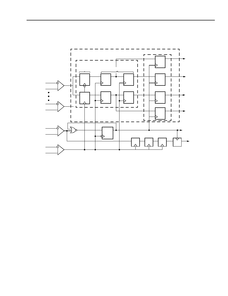
Agere Systems Inc.
35
Data Sheet
August 2001
Eight-Channel x 850 Mbits/s Backplane Transceiver
ORCA ORT8850 FPSC
RapidIO Interface to Pi-Sched
(continued)
0676
Figure 14. RapidIO Receive Cell Interface
Octets and Start of Cell
Cells will be transmitted on the high-speed LVDS inputs as octets. The first octet o0 (consisting of
d0_0, d1_0 . . . d7_0) will be present on bits 31:24 on the low-speed 32-bit FPGA bus. Similarly, octet o1 (consist-
ing of d0_1, 1_1 . . . d7_1) will be present on bits 23:16 on the 32-bit bus. Thus, octets will always be transmitted
from first octet to last. The minimum number of octets present on the high-speed ports should always be divisible
by 4, evenly representing the relationship with the 32-bit core of the ASIC interface. The start-of-cell signal is
always aligned with the first octet of each cell. Once the first octet of a cell is received, subsequent octets are part
of an uninterrupted data stream until the entire cell has been received. The number of octets in a cell is determined
by the register bits OCELLSIZE. The RapidIO can support varying minimum cell sizes from four octets up to 124 in
increments of 4. The RapidIO is programmed with the cell size by writing to the OCELLSIZE register via the micro-
processor interface. If the transmitted cell size is less than the programmed cell size, a violation occurs and the
IRXSOCVIOL flag is active. This flag can be ignored if a given minimum cell size is not needed.
D
CLK
Q
RXCLK
RXSOC
D
CK
Q
ZRXD_7
ZRXD_23
ZRXD_31
ZRXD_15
WRXCLK
(133 MHz)
TO
FPGA
133 MHz CLOCK DOMAIN
266 MHz CLOCK DOMAIN
INPUT
REPEATED 7 TIMES (ONE FOR EACH OF RXD[1:7])
D
Q
ZRXSOC
D
Q
D
Q
D
Q
RXD[7]
RXD[0]
ZRXD_15
D
CLK
Q
DATA
CAPTURE
SHIFT REGISTERS
D
CK
Q
D
CK
Q
D
CK
Q
D
CK
Q
D
CK
Q
D
CK
Q
D
CK
Q
D
CK
Q
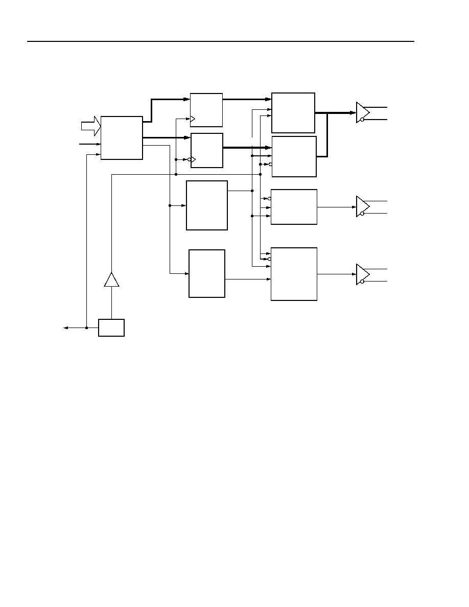
36
Agere Systems Inc.
Data Sheet
August 2001
Eight-Channel x 850 Mbits/s Backplane Transceiver
ORCA ORT8850 FPSC
RapidIO Interface to Pi-Sched
(continued)
0677
Figure 15. RapidIO Transmit Cell Interface
Transmit Cell Interface
The transmit interface performs multiplexing of 32 bits of low-speed data onto four sequential octets of eight pairs
of LVDS signal pins using both edges of a high-speed clock. The transmitter module consists of the following
ten LVDS signal pairs (see Figure 15):
s
Eight LVDS data pairs (TXD), double-edge clocked by the LVDS clock TXCLK. The data pairs carry biphase data
at 120 MHz--311 MHz.
s
One start-of-cell LVDS pair that indicates that octet 0 of a data cell is on TXD. The transitions of this signal are at
90 degrees also with the crossing points of the LVDS clock (TXCLK).
s
One LVDS clock pair output TXCLK operating at 120 MHz--311 MHz. Its relationship is intended to be exactly in
90 degree phase with the transitions of TXD data and TXSOC.
The high-speed data outputs (TXD[0:7]) as well as the start-of-cell signal TXSOC are generated as a result of the
positive edge of PFCLK. This is accomplished by multiplexing between the even and odd bytes of the data at a
1/2 PFCLK rate. PFCLK is derived from the internal PLL and operates at 4x the base frequency or between
240 MHz and 284 MHz. The PFCLK is expected to have a duty cycle of 47% to 53% with no more than
±
150 ps of
jitter. The duty cycle of PFCLK will directly affect the accuracy of the high-speed clock and its ability to maintain the
eye of the data. The 90 degree phase shift of the output clock puts TXCLK in the eye of the data.
COMMON
TRANSMIT
FIFO
EVEN BYTE
ODD BYTE
EVEN BYTE
UTXD
[31:0]
UTXSOC
WUTXCLK
(60 MHz--146 MHz)
OUTPUT
PORT CLOCK
ALIGNMENT
MUX
OUTPUT
PORT SOC
ALIGNMENT
MUX
F
P
GA
I/F
PFCLK (4x OUTPUT CLOCK FROM PLL)
32 TO 8
INPUT
SOC
REGISTER
SOC
TXSOC
(240 MHz--584 MHz)
O
F
F
-
CHI
P
INT
E
RF
A
C
E
PLL
POSITIVE-
OUTPUT
PORT DATA
ALIGNMENT
MUXes
MUX
CONTROLLER
TXCLK
TXD[7:0]
ODD BYTE
OUTPUT
PORT DATA
ALIGNMENT
MUXes
EDGE
FLOPS
NEGATIVE-
EDGE
FLOPS

Agere Systems Inc.
37
Data Sheet
August 2001
Eight-Channel x 850 Mbits/s Backplane Transceiver
ORCA ORT8850 FPSC
RapidIO Interface to Pi-Sched
(continued)
Table 8. RapidIO Signals to/from FPGA
Interface Name
(All End with _A, _B, or
_C Depending on
Channel)
From
FPGA
To FPGA
Description
Receive Cell Interface
ZRXD<31:0>
--
32
32-bit data from the receive module. The bus contains four
octets and reflects data received via the high-speed RXD data
bus.
ZRXSOC
--
1
Indicates the presence of the first octet of a new cell within the
first 32-bit data word on the bus RXD in bit positions [31:24].
ZRXSOCVIOL
--
1
Indicates a minimum cell violation within the receive module.
This signal will transition active-high coincident with RXSOC.
An active state signals the new cell overran the previous cell,
and the previous cell is in violation of the minimum cell size.
ZRXALNVIOL
--
1
Signals an alignment error. An active state signals RXSOC was
captured on a negative RXCLK edge. The violation condition
on this signal will stay high for a single
WRXCLK_[chan]_FPGA cycle coincident with RXSOC.
ZCLKSTAT
--
--
Indicates the loss or absence of a clock on the LVDS clock
(RXCLK). This signal will be present for the duration of the
absence of the clock, following a period to validate its absence.
CSYSENB
1
--
System cell processing enable. After reset is released, drive
this signal high when the RapidIO is ready to transmit cells.
This signal should be active after all control signals into the
RapidIO are stable.
RSTN_RX
1
--
Synchronous reset for all memory elements clocked by
WRXCLK_[chan]_FPGA (derived from PLL).
WRXCLK_[chan]_FPGA
--
1
Derived from high-speed LVDS clock RXCLK (RXCLK/2).
Transmit Cell Interface
UTXD[31:0]
32
--
Transmit data bs containing four octets synchronized with the
rising edge of the 60 MHz--146 MHz WUTXCLK_FPGA
(derived from PLL) is clocked into the transmit FIFO within the
RapidIO.
UTXSOC
1
--
Start of cell, originating within core, synchronized with the ris-
ing edge of WUTXCLK_FPGA into the transmit FIFO. Indicates
the first data word on TXD bus includes the first octet of a new
cell in bit positions [31:24].
RSTN_UTX
1
--
Synchronous reset for all memory elements in the WUTXCLK
domain.
UTXTRISTN
1
--
Output 3-state enable (active-low). When active, the TXD,
TXSOC, and TXCLK LVDS drivers are 3-stated.
0: 3-state TXD, TXSOC and TXCLK drivers.
1: Normal operation.
FPGA Interface Clocks (Common to All Channels)
WUTXCLK_FPGA
--
1
One X core clock generated from an internal PLL circuit. Syn-
chronous to UTXD and UTXSOC data inputs.
HALFCLK_FPGA
--
1
1/2 X main PLL output clock. Phase-aligned with PFCLK. Nom-
inal frequency = 30 MHz to 73 MHz. Duty cycle spec = 47%/
53%.

38
Agere Systems Inc.
Data Sheet
August 2001
Eight-Channel x 850 Mbits/s Backplane Transceiver
ORCA ORT8850 FPSC
RapidIO Interface to Pi-Sched
(continued)
Table 9. Signals Used as Register Bits
Memory Map
Definition of Register Types
There are six structural register elements: sreg, creg, preg, iareg, isreg, and iereg. There are no mixed registers in
the chip. This means that all bits of a particular register (particular address) are structurally the same. All of these
registers are accessed via the FPGA system bus which, in turn, can be accessed by the MPI block or through
FPGA logic.
Register Bit(s)
Description
OSHLBENB
Used during the internal built-in self-test mode. Indicates that the single-ended versions of the
transmit module outputs should be looped back into the single-ended inputs of the receive
module.
OSHLENB = 0: No loopback.
OSHLENB = 1: Loopback.
OCELLSIZE[4:0] This value indicates the minimum cell size and will be used to detect cell underrun errors. This
value should be set and stable prior to initialization of operation and stable thereafter.
OTESTENB
Enables the internal self-test of the RapidIO block. Two loopback paths exist during test, inter-
nal and external. During both tests, data is passed through all modules and verified.
ITESTDONE
Indicates the completion of the internal test. Only valid during a test when OTESTENB is high.
ITESTDONE = 0: Test running.
ITESTDONE = 1: Test complete.
ITESTPASS
Indicates the success of the internal test. This signal is valid only when ITESTDONE is high.
ITESTPASS = 0: Test failed.
ITESTPASS = 1: Test passed.
TRISTN
Active-low. 3-state override for transmit outputs. This signal is ignored during reset, but takes
priority over all 3-state control signals when active.

Agere Systems Inc.
39
Data Sheet
August 2001
Eight-Channel x 850 Mbits/s Backplane Transceiver
ORCA ORT8850 FPSC
Memory Map
(continued)
Table 10. Structural Register Elements
Registers Access and General Description
The memory map comprises three address blocks:
s
Generic register block: ID, revision, scratch pad, lock, FIFO alignment, and reset registers.
s
Device register block: control and status bits, common to the four channels in each of the two quad interfaces.
s
Channel register blocks: each of the four channels in both quads have an address block. The four address
blocks in both quads have the same structure, with a constant address offset between channel register blocks.
All registers are write-protected by the lock register, except for the scratch pad register. The lock register is a 16-bit
read/write register. Write access is given to registers only when the key value 0x0580 is present in the lock register.
An error flag will be set upon detecting a write access when write permission is denied. The default value is
0x0000.
After powerup reset or soft reset, unused register bits will be read as zeros. Unused address locations are also
read as zeros. Write-only register bits will be read as zeros. The detailed information on register access and func-
tion are described on the tables, memory map, and memory map bit description.
A memory map is included in Table 11, followed by detailed descriptions in Table 11. These tables list only the
memory map for the core registers of the ORT8850 device. The remaining FPGA registers can be found in the
Series 4 data sheet.
Element
Register
Description
sreg
Status
Register
A status register is read only, and, as the name implies, is used to convey the status
information of a particular element or function of the ORT8850 core. The reset value of
an sreg is really the reset value of the particular element or function that is being read.
In some cases, an sreg is really a fixed value; an example of which is the fixed ID and
revision registers.
creg
Control
Register
A control register is read and writable memory element inside core control. The value of
a creg will always be the value written to it. Events inside the ORT8850 core cannot
affect creg value. The only exception is a soft reset, in which case the creg will return to
its default value.
preg
Pulse
Register
Each element, or bit, of a pulse register is a control or event signal that is asserted and
then deasserted when a value of one is written to it. This means that each bit is always
of value 0 until it is written to, upon which it is pulsed to the value of one and then
returned to a value of 0. A pulse register will always have a read value of 0.
iareg
Interrupt Alarm
Register
Each bit of an interrupt alarm register is an event latch. When a particular event is pro-
duced in the ORT8850 core, its occurrence is latched by its associated iareg bit. To
clear a particular iareg bit, a value of one must be written to it. In the ORT8850 core, all
isreg reset values are 0.
isreg
Interrupt Status
Register
Each bit of an interrupt status register is physically the logical-OR function. It is a con-
solidation of lower-level interrupt alarms and/or isreg bits from other registers. A direct
result of the fact that each bit of the isreg is a logical-OR function means that it will have
a read value of one if any of the consolidation signals are of value one, and will be of
value 0 if and only if all consolidation signals are of value 0. In the ORT8850 core, all
isreg default values are 0.
ereg
Interrupt Enable
Register
Each bit of a status register or alarm register has an associated enable bit. If this bit is
set to value one, then the event is allowed to propagate to the next higher level of con-
solidation. If this bit is set to zero, then the associated iareg or isreg bit can still be
asserted but an alarm will not propagate to the next higher level. An interrupt enable bit
is an interrupt mask bit when it is set to value 0.
40
Agere Systems Inc.
Data Sheet
August 2001
Eight-Channel x 850 Mbits/s Backplane Transceiver
ORCA ORT8850 FPSC
Memory Map
(continued)
This table is constructed to show the correct values when read and written via the system bus MPI interface. When
using this table while interfacing with the system bus user logic master interface, the data values will need to be
byte flipped. This is due to the opposite orientation of the MPI and master interface bus ordering. More information
on this can be found in the MPI/System Bus Application Note (AP01-032NCIP).
Table 11. Memory Map (This table resides at memory offset 0X30000 in the ORT8850.)
ADDR
[7:0]
Register
Type
DB7
DB6
DB5
DB4
DB3
DB2
DB1
DB0
MSB
Reset
Value
[7:0]
Comment
00
sreg
fixed rev [0:7]
05
ge
n
e
r
i
c r
e
gi
st
er
b
l
oc
k
01
sreg
fixed id lsb [0:7]
80
02
sreg
fixed id msb [0:7]
80
03
creg
scratch pad [0:7]
00
04
creg
lockreg msb [0:7]
00
05
creg
lockreg lsb [0:7]
00
06
preg
--
--
--
--
--
--
--
global
reset
comman
d
NA
Device Register Block
08
creg
--
--
--
"rx toh
frame"
and "rx
toh clk
enable"
hiz
control
ext prot
sw en
--
--
lvds lpbk
control
(CDR
only)
00
de
vi
ce
r
e
g
.
bl
k
-
rx
09
creg
parallel
port
output
MUX
select for
ch#7
parallel
port
output
MUX
select for
ch#5
serial
port
output
MUX
select for
ch#7
serial port
output
MUX
select for
ch#5
parallel
port
output
MUX
select for
ch#3
parallel
port
output
MUX
select for
ch#1
serial
port
output
MUX
select for
ch#3
serial
port
output
MUX
select for
ch#1
FF (4 ch
was 0F)
0a
creg
--
--
--
FIFO aligner threshold value (min) [0:4]
40
0b
creg
--
--
--
FIFO aligner threshold value (max) [0:4]
A8
0c
creg
--
scram-
bler/
descra-
mbler
control
input/
output
parallel
bus
parity
control
line lpbk
control
number of consecutive A1 A2 errors to
generate [0:3]
06
de
vi
ce
r
e
g
b
l
k
-
t
x
0d
creg
a1 error insert value [0:7]
00
0e
creg
a2 error insert value [0:7]
00
0f
creg
transmitter B1 error insert mask [0:7]
00

Agere Systems Inc.
41
Data Sheet
August 2001
Eight-Channel x 850 Mbits/s Backplane Transceiver
ORCA ORT8850 FPSC
Memory Map
(continued)
Table 11. Memory Map (continued)
ADDR
[7:0]
Register
Type
DB7
DB6
DB5
DB4
DB3
DB2
DB1
DB0
MSB
Reset
Value
[7:0]
Comment
10
isreg
--
--
--
per
device
int
ch 4 int
ch 3 int
ch 2 int
ch 1 int
00
to
p
-
le
v
e
l i
n
t
e
r
r
u
p
t
s
11
iereg
--
--
--
enable/mask register [0:4]
00
12
iareg
--
--
--
--
--
--
write to
locked
register
error flag
frame
offset
error flag
00
13
iereg
--
--
--
--
--
--
enable/mask
register [6:7]
00
14
isreg
--
--
--
--
ch 8 int
ch 7 int
ch 6 int
ch 5 int
00
15
iereg
--
--
--
--
enable/mask register [0:3]
00
16
creg
--
--
--
--
STM-A
mode
control
STM-A
mode
control
STM-B
mode
control
STM-B
mode
control
0x00
--
17
creg
STM A
Stream
A
resync.
STM A
Stream B
resync
STM A
Stream
C resync
STM A
Stream
D resync
STM B
Stream
A resync
STM B
Stream
B resync
STM B
Stream C
resync
STM B
Stream
D resync
00
--
18
creg
--
STM A
and B
resync
(all 8
streams
AA to BD)
STM A
Resync
(all 4
streams
AA, AB,
AC and
AD)
STM B
Resync
(all 4
streams
BA, BB,
BC and
BD)
Twins
AA
Resync
(streams
AA and
BA)
Twins
BB
resync
(streams
AB and
BB)
Twins CC
resync
(streams
AC and
BC)
Twins
DD
resync
(streams
AD and
BD)
00
--
Channel Register Block
20, 38,
50, 68,
80, 98,
b0, c8
creg
hi-z
control
of TOH
data
output
hi-z
control of
parallel
output
bus
channel
enable/
disable
control
parallel
output
bus
parity err
ins cmd
rx k1/k2
source
select
TOH
serial
output
port par
err ins
cmd
force ais-l
control
rx
behavior
in lof
80
rx
co
nt
ro
l
s
i
gna
l
s
21, 39,
51, 69,
81, 99,
b1, c9
creg
tx mode
of
operatio
n
tx e1 f1
e2 source
select
tx s1 m0
source
select
tx k1 k2
source
select
tx d12
source
select
tx d11
source
select
tx d10
source
select
tx d9
source
select
00
t
x
c
ont
r
o
l
s
i
gna
l
s
22, 3a,
52, 6a,
82, 9a,
b2, ca
creg
tx d8
source
select
tx d7
source
select
tx d6
source
select
tx d5
source
select
tx d4
source
select
tx d3
source
select
tx d2
source
select
tx d1
source
select
00
23, 3b,
53, 6b,
83, 9b,
b3, cb
creg
--
--
--
--
disable
A1/A2
insert
disable
B1 insert
b1 error
insert
comman
d
a1 a2
error ins
comman
d
00

42
Agere Systems Inc.
Data Sheet
August 2001
Eight-Channel x 850 Mbits/s Backplane Transceiver
ORCA ORT8850 FPSC
Memory Map
(continued)
Table 11. Memory Map (continued)
* The FIFO aligner threshold error flag is only valid if a FIFO out of sync error flag is also present.
ADDR
[7:0]
Register
Type
DB7
DB6
DB5
DB4
DB3
DB2
DB1
DB0
MSB
Reset
Value
[7:0]
Comment
24, 3c,
54, 6c,
84, 9c,
b4, cc
sreg
--
--
--
--
Concat
indication
12
Concat
indication
9
Concat
indication
6
Concat
indication
3
NA
per st
s
#1
cos
f
l
a
g
25, 3d,
55, 6d,
85, 9d,
b5, cd
sreg
Concat
indication
11
Concat
indication
8
Concat
indication
5
Concat
indication
2
Concat
indication
10
Concat
indication
7
Concat
indication
4
Concat
indication
1
NA
26, 3e,
56, 6e,
86, 9e,
b6, ce
isreg
--
--
--
--
--
elastic
store
overflow
flag
ais-p flag
per sts-12
alarm flag
00
per channel
i
n
t
e
rrup
t
consolidat
i
o
n
27, 3f,
57, 6f,
87, 9f,
b7, cf
iereg
--
--
--
--
--
enable/mask register [0:3]
00
28, 40,
58, 70,
88, a0,
b8, d0
iareg
--
FIFO
(Out of
Sync)
error flag
TOH
serial
input port
parity
error flag
input
parallel
bus parity
error flag
LVDS link
B1 parity
error flag
LOF flag
Receiver
internal
path
parity
error flag
FIFO*
aligner
threshold
error flag
00
per
s
t
s-
12
i
n
t
e
rru
pt
f
l
ags
29, 41,
59, 71,
89, a1
b9, d1
iereg
--
--
enable/mask register [0:5]
00

Agere Systems Inc.
43
Data Sheet
August 2001
Eight-Channel x 850 Mbits/s Backplane Transceiver
ORCA ORT8850 FPSC
Memory Map
(continued)
Table 11. Memory Map (continued)
ADDR
[7:0]
Register
Type
DB7
DB6
DB5
DB4
DB3
DB2
DB1
DB0
MSB
Reset
Value
[7:0]
Comments
2a, 42,
5a, 72,
8a, a2,
ba, d2
iareg
--
--
--
--
AIS
interrupt
flags
12
AIS
interrupt
flag
9
AIS
interrupt
flags
6
AIS
interrupt
flags
3
00
pe
r
st
s
-
1
i
n
t
e
r
r
upt
f
l
a
g
s
2b, 43,
5b, 73,
8b, a3,
bb, d3
iareg
AIS
interrupt
flag
11
AIS
interrupt
flag
8
AIS
interrupt
flag
5
AIS
interrupt
flag
2
AIS
interrupt
flag
10
AIS
interrupt
flag
7
AIS
interrupt
flag
4
AIS
interrupt
flag
1
00
2c, 44,
5c, 74,
8c, a4,
bc, d4
iereg
--
--
--
--
enable/
mask
AIS
interrupt
flags
12
enable/
mask
AIS
interrupt
flag
9
enable/
mask
AIS
interrupt
flags
6
enable/
mask
AIS
interrupt
flags
3
00
2d, 45,
5d, 75,
8d, a5,
bd, d5
iereg
enable/
mask
AIS
interrupt
flag
11
enable/
mask
AIS
interrupt
flag
8
enable/
mask
AIS
interrupt
flag
5
enable/
mask
AIS
interrupt
flag
2
enable/
mask
AIS
interrupt
flag
10
enable/
mask
AIS
interrupt
flag
7
enable/
mask
AIS
interrupt
flag
4
enable/
mask
AIS
interrupt
flag
1
00
2e, 46,
5e, 76,
8e, a6,
be, d6
iareg
--
--
--
--
ES
overflow
flags
12
ES
overflow
flag
9
ES
overflow
flags
6
ES
overflow
flags
3
00
2f, 47,
5f, 77,
8f, a7,
bf, d7
iareg
ES
overflow
flag
11
ES
overflow
flag
8
ES
overflow
flag
5
ES
overflow
flag
2
ES
overflow
flag
10
ES
overflow
flag
7
ES
overflow
flag
4
ES
overflow
flag
1
00
30, 48,
60, 78,
90, a8,
c0, d8
iereg
--
--
--
--
enable/
mask ES
overflow
flags
12
enable/
mask ES
overflow
flag
9
enable/
mask ES
overflow
flags
6
enable/
mask ES
overflow
flags
3
00
--
31, 49,
61, 79,
91, a9,
c1, d9
iereg
enable/
mask ES
overflow
flag
11
enable/
mask ES
overflow
flag
8
enable/
mask ES
overflow
flag
5
enable/
mask ES
overflow
flag
2
enable/
mask ES
overflow
flag
10
enable/
mask ES
overflow
flag
7
enable/
mask ES
overflow
flag
4
enable/
mask ES
overflow
flag
1
00
--

44
Agere Systems Inc.
Data Sheet
August 2001
Eight-Channel x 850 Mbits/s Backplane Transceiver
ORCA ORT8850 FPSC
Memory Map
(continued)
Table 11. Memory Map (continued)
ADDR
[7:0]
Register
Type
DB7
DB6
DB5
DB4
DB3
DB2
DB1
DB0
MSB
Reset
Value
[7:0]
Comments
32, 4a,
62, 7a,
92, aa,
c2, da
counter
overflow
LVDS link b1 BIP-8 parity error counter
00
bi
n
n
i
n
g
33, 4b,
63, 7b,
93, ab,
c3, db
counter
overflow
LOF counter
00
34, 4c,
64, 7c,
94, ac,
c4, dc
counter
overflow
A1 A2 frame error counter
00
35, 4d,
65,
7d,
95,
ad,
c5, dd
creg
Reserved
--
--
FIFO depth register
0x0c
--
36, 4e,
66, 7e,
96, ae,
c6, de
counter
Sampler phase error count
00
--
37, 4f,
67, 7f,
97, af,
c7, df
creg
--
--
Framer
Disable
Sync control
LVDS
redun-
dant
select
Bypass
Alignment
FIFO +
Pointer
Mover
Bypass
Pointer
Mover
00
--
CDR Specific Registers
e0
creg
TST
MODE
BYPASS
LOOP
BKEN
TST
PHASE
--
EN10BIT
Shim
Mode
--
--
e3
creg
ENCOMMA[0:7]
--
--
Pi-Sched Registers
f0
creg
--
RapidIO
(shim)
Loopback
enable
OPIMODE
(Reserved)
OCELLSIZE[3:7]
--
--
f1
sreg
--
--
--
--
--
--
ITESTDO
NE
ITEST
PASS
0
--
f2
creg
--
--
--
--
--
--
IBYPASS
OTEST
ENB
--
--
Agere Systems Inc.
45
Data Sheet
August 2001
Eight-Channel x 850 Mbits/s Backplane Transceiver
ORCA ORT8850 FPSC
Memory Map
(continued)
Table 12. Memory Map Descriptions
Bit/Register
Name(S)
Bit/
Register
Location
(Hex)
Register
Type
Reset
Value
(Hex)
Description
fixed rev [0:7]
fixed id lsb [0:7]
fixed id msb [7:0]
00 [0:7]
01 [0:7]
02 [0:7]
sreg
05
80
80
NA
scratch pad [0:7]
03 [0:7]
creg
00
The scratch pad has no function and is not used anywhere in
the core. However, this register can be written to and read from.
lockreg msb [0:7]
lockreg lsb [0:7]
04 [0:7]
05 [0:7]
creg
00
00
In order to write to registers in memory locations 06~7F, lockreg
msb and lockreg lsb must be respectively set to the values of
05 and 80. If the msb and lsb lockreg values are not set to {05,
80}, then any values written to the registers in memory loca-
tions 06~7F will be ignored.
After reset (both hard and soft), the core is in a write locked
mode. The core needs to be unlocked before it can be written
to.
Also note that the scratch pad register (03) can always be writ-
ten to as it is unaffected by write lock mode.
global reset com-
mand
06 [0]
preg
NA
The global reset command is accessed via the pulse register in
memory address 06. The global reset command is a soft (soft-
ware initiated) reset. Nevertheless, the global reset command
will have the exact reset effect as a hard (RST_N pin) reset.
Device Register Blocks
lvds lpbk control
08 [0]
creg
0
ext prot sw en
08 [3]
creg
0
"rx toh frame" and
"rx toh clk enable"
hiz control
08 [4]
creg
0
CDR
0
No loopback.
1
LVDS loopback, transmit to receive on. Serieal data is looped
back to the rx serial input.
ext port
sw en
LVDS Protection Switching
0
- MUX is controlled by software (1 control bit per MUX) reg 09.
- Output buffers' enables are controlled by software (1 control bit per chan-
nel) reg 20, 38, 50, 68, 80, 98, b0, c8.
1
MUX is controlled by hardware pins.
lvds_Prot_Switch_[aa,ab,ac,ad,ba,bb,bc,bd]
0
TOH_CK_FP_EN = 0, can be used to 3-state RX_TOH_CK_EN and RX_TOH_FP signals.
1
Function mode.
46
Agere Systems Inc.
Data Sheet
August 2001
Eight-Channel x 850 Mbits/s Backplane Transceiver
ORCA ORT8850 FPSC
Memory Map
(continued)
Table 12. Memory Map Descriptions
(continued)
Bit/Register Name(S)
Bit/ Register
Location
(Hex)
Register
Type
Reset
Value
(Hex)
Description
serial port output MUX
select for ch#1
serial port output MUX
select for ch#3
parallel port output MUX
select for ch#1
parallel port output MUX
select for ch#3
serial port output MUX
select for ch#5
parallel port output MUX
select for ch#7
serial port output MUX
select for ch#5
parallel port output MUX
select for ch#7
09 [0]
09 [1]
09 [2]
09 [3]
09 [4]
09 [5]
09 [6]
09 [7]
creg
1
1
1
1
FIFO aligner threshold
value (min) Default = 2
FIFO aligner threshold
value (max) Default = 15
0A [0:4]
0B [0:4]
creg
40
A8
These are the minimum and maximum thresholds
values for the per channel receive direction align-
ment FIFOs. If and when the minimum or maximum
threshold value is violated by a particular channel,
then the interrupt event "FIFO aligner threshold
error" will be generated for that channel and latched
as a "FIFO aligner threshold error flag" in the
respective per STS-12 interrupt alarm register.
The allowable range for minimum threshold values
is 1 to 23.
The allowable range for maximum threshold values
is 0 to 22.
Note that the minimum and maximum FIFO aligner
threshold values apply to all four channels.
number of consecutive
A1 A2 errors to generate
[0:3]
A1 error insert value
[0:7]
A2 error insert value
[0:7]
0C [0:3]
0D [0:7]
0E [0:7]
creg
00
00
00
These three per device control signals are used in
conjunction with the per channel "a1 a2 error insert
command" control bits to force A1 A2 errors in the
transmit direction.
If a particular channel's "a1 a2 error insert com-
mand" control bit is set to the value 1 then the "A1
and A2 error insert values" will be inserted into that
channels respective A1 and A2 bytes. The number
of consecutive frames to be corrupted is deter-
mined by the "number of consecutive A1 A2 errors
to generate[0:3]" control bits.
The error insertion is based on a rising edge detec-
tor. As such the control must be set to value 0
before trying to initiate a second a1 a2 corruption.
backplane side loop-
back control
0C [4]
creg
0
serial port output MUX
0
TOH output is multiplexed to next channel.
1
TOH output is multiplexed to same channel.
parallel port output
0
Parallel output data bus is multiplexed to
next channel.
1
Parallel output data bus is multiplexed to
same channel
0
No loopback.
1
rx to tx loopback on backplane side. Serial input is run through
SERDES and looped back in parallel to SERDES and out
serial.
Agere Systems Inc.
47
Data Sheet
August 2001
Eight-Channel x 850 Mbits/s Backplane Transceiver
ORCA ORT8850 FPSC
Memory Map
(continued)
Table 12. Memory Map Descriptions
(continued)
Bit/Register Name(S)
Bit/
Register
Location
(Hex)
Register
Type
Reset
Value
(Hex)
Description
input/output parallel bus
parity control
0C [5]
creg
1
scrambler/descrambler
control
0C [6]
creg
1
transmit B1 error insert
mask [0:7]
0F [0:7]
creg
00
ch 1 int
ch 2 int
ch 3 int
ch 4 int
per device int
enable/mask register for
ch 1-4 + device[4:0]
ch 5 int
ch 6 int
ch 7 int
ch 8 int
enable/mask register for
ch 5-8 [0:3]
10 [0]
10 [1]
10 [2]
10 [3]
10 [4]
11 [0:4]
14 [0]
14 [1]
14 [2]
14 [3]
15 [0:3]
isreg
isreg
isreg
isreg
isreg
iereg
isreg
isreg
isreg
isreg
iereg
0
0
0
0
0
0
0
0
0
0
0
Consolidation interrupts. 1 = interrupt, 0 = no interrupt.
frame offset error flag
write to locked register
error flag
enable/mask register [0:1]
12 [0]
12 [1]
13 [0:1]
iareg
iareg
iereg
0
0
0
If in the receive direction the phase offset between any two
channels exceeds 17 bytes, then a frame offset error event
will be issued. This condition is continuously monitored.
If the core memory map has not been unlocked (by writing
to the lock registers), and any address other than the lock-
reg registers or scratch pad register is written to, then a
"write to locked register" event will be generated.
STM A mode control
STM B mode control
16 [2:3]
16 [0:1]
creg
creg
0
0
00 - Quad STS-12 or STS-48.
01 - Quad STS-3.
10 - Quad STS-1.
00 - Quad STS-12 or STS-48.
01 - Quad STS-3.
10 - Quad STS-1.
individual alignment
resync register
17 [0:7]
creg
0
Write 1 to resync stream.
group alignment resync
register
18 [0:7]
creg
0
Write 1 to resync selected grouping.
0
Even parity.
1
Odd parity.
0
no rx direction, descramble / tx direction scramble.
1
In rx direction, descramble channel after SONET frame recov-
ery.
In tx direction, scramble data just before parallel-to-serial con-
version.
0
No error insertion.
1
Invert corresponding bit in B1 byte.
48
Agere Systems Inc.
Data Sheet
August 2001
Eight-Channel x 850 Mbits/s Backplane Transceiver
ORCA ORT8850 FPSC
Memory Map
(continued)
Table 12. Memory Map Descriptions
(continued)
Bit/Register Name(S)
Bit/
Register
Location
(Hex)
Register
Type
Reset
Value
(Hex)
Description
Channel Register Blocks
rx behavior in lof
force ais-l control
20, 38, 50,
68,
80, 98, b0,
c8 [0]
20, 38, 50,
68,
80, 98, b0,
c8 [1]
--
1
0
TOH serial output port par err
ins cmd
20, 38, 50,
68,
80, 98, b0,
c8 [2]
--
0
rx k1/k2 source select
20, 38, 50,
68, 80, 98,
b0, c8 [3]
--
0
parallel output bus parity err
ins cmd
20, 38, 50,
68, 80, 98,
b0, c8 [4]
--
0
channel enable/disable control
hi-z control of parallel output
bus
hi-z control of TOH data output
20, 38, 50,
68, 80, 98,
b0, c8 [5]
20, 38, 50,
68, 80, 98,
b0, c8 [6]
20, 38, 50,
68, 80, 98,
b0, c8 [7]
creg
creg
creg
0
0
0
rx behavior in log
0
When Rx direction OOF occurs, do not insert
AIS-L.
1
When Rx direction OOF occurs, insert AIS-L.
force ais-l control
0
Do not force AIS-L.
1
Force AIS-L.
0
Do not insert a parity error.
1
Insert parity error in parity bit of receive TOH serial output for
as long as this bit is set.
0
Set receive direction K2 K2 bytes to 0.
1
Pass receive direction K1 K2 though pointer mover.
0
Do not insert parity error.
1
Insert parity error in the parity bit of receive direction parallel
output bus for as long as this bit is set.
channel
enable / dis-
able control
0
Power down CDR channels (PWR_DN_A/B/C/
D_N=0). TOH_EN_A(or B, C, D)=0, and
DOUTA(or B, C, D)=0, can be used to 3-state out-
put buses.
1
Functional mode.
hi-z control of
parallel output
bus
0
DOUTA(or B, C, D) _EN=0, can be used to 3-state
output bus.
1
Functional mode.
hi-z control of
TOH data out-
put
0
TOH_EN_A(or B, C, D)=0, can be used to 3-state
TOH output lines.
Agere Systems Inc.
49
Data Sheet
August 2001
Eight-Channel x 850 Mbits/s Backplane Transceiver
ORCA ORT8850 FPSC
Memory Map
(continued)
Table 12. Memory Map Descriptions
(continued)
Bit/Register Name(S)
Bit/Register
Location
(Hex)
Register
Type
Reset
Value
(Hex)
Description
tx mode of operation
tx e1 f2 e2 source select
tx s1 m0 source select
tx k1 k2 source select
tx d12~d9 source select
tx d8~d1 source select
21, 39, 51,
69, 81, 99,
b1, c9 [7]
21, 39, 51,
69, 81, 99,
b1, c9 [6]
21, 39, 51,
69, 81, 99,
b1, c9 [5]
21, 39, 51,
69, 81, 99,
b1,c9 [4:0]
22, 3a, 52,
6a,
82, 9a, b2, ca
[7:0]
creg
creg
creg
creg
creg
0
0
0
0
00
a1 a2 error insert command
b1 error insert command
disable b1 insert
disable a1 insert
23, 3b, 53,
6b, 83, 9b,
b3, cb [0]
23, 3b, 53,
6b, 83, 9b,
b3, cb [1]
23, 3b, 53,
6b, 83, 9b,
b3, cb [2]
23, 3b, 53,
6b, 83, 9b,
b3, cb [3]
creg
creg
0
0
concat indication 12, 9, 6, 3
concat indication 11, 8, 5, 2,
10, 7, 4, 1
24, 3c, 54,
6c, 84, 9c,
b4, cc [0:3]
25, 3d, 55,
6d, 85, 9d,
b5, cd [0:7]
sreg
sreg
0
0
The value 1 in any bit location indicates that STS# is in CONCAT
mode. A 0 indicates that the STS in not in CONCAT mode, or is the
head of a concat group.
Tx mode of operation:
Other registers:
0
Insert TOH from serial ports on FPGA interface.
1
Pass through all TOH of parallel stream.
0
Insert TOH from serial ports on FPGA interface.
1
Pass through that particular TOH byte.
The error insertion is based on a rising edge detector. As such,
the control must be set to value 0 before trying to initiate a sec-
ond a1 a2 corruption.
The error insertion is based on a rising edge detector. As such,
the conrtol mustbe set to value 0 before trying to initiate a second
0
Do not insert error.
1
Insert error for number of frames in register hex 0C.
0
Do not insert error.
1
Insert error for 1 frame in B1 bits defined by register hex 0F.

50
Agere Systems Inc.
Data Sheet
August 2001
Eight-Channel x 850 Mbits/s Backplane Transceiver
ORCA ORT8850 FPSC
Memory Map
(continued)
Table 12. Memory Map Descriptions
(continued)
Bit/Register Name(S)
Bit/
Register
Location
(Hex)
Register
Type
Reset
Value
(Hex)
Description
per sts-12 alarm flag
ais-p flag
elastic store overflow flag
enable/mask register [0:5]
26, 3e,
56, 6e,
86, 9e,
b6, ce [0]
26, 3e,
56, 6e,
86, 9e,
b6, ce [1]
26, 3e,
56, 6e,
86, 9e,
b6,ce [2]
27, 3f,
57, 6f,
87, 9f,
b7, cf
[5:7]
isreg
isreg
isreg
iereg
0
0
0
0
These flag register bits per STS-12 alarm flag, ais-p
flag, and elastic store overflow flag are the per-chan-
nel interrupt status (consolidation) register.

Agere Systems Inc.
51
Data Sheet
August 2001
Eight-Channel x 850 Mbits/s Backplane Transceiver
ORCA ORT8850 FPSC
Memory Map
(continued)
Table 12. Memory Map Descriptions
(continued)
Bit/Register Name(S)
Bit/Register
Location (Hex)
Register
Type
Reset
Value
(Hex)
Description
FIFO aligner threshold
error flag
receiver internal path par-
ity error flag
LOF flag
LVDS link B1 parity error
flag
input parallel bus parity
error flag
TOH serial input port par-
ity error flag
FIFO OOS error flag
enable/mask register [0:5]
28, 40, 58, 70,
88, a0, b8, d0 [0]
28, 40, 58, 70,
88, a0, b8, d0 [1]
28, 40, 58, 70,
88, a0, b8, d0 [2]
28, 40, 58, 70,
88, a0, b8, d0 [3]
28, 40, 58, 70,
88, a0, b8, d0 [4]
28, 40, 58, 70,
88, a0, b8, d0 [5]
28, 40, 58, 70,
88, a0, b8, d0 [6]
29, 41, 59, 71,
89, a1, b9, d1
[0:5]
iareg
iareg
iareg
iareg
iareg
iareg
iereg
0
0
0
0
0
0
00
These are the per STS-12 alarm flags.
Loss of frame.
FIFO out of Sysc error flag.

52
Agere Systems Inc.
Data Sheet
August 2001
Eight-Channel x 850 Mbits/s Backplane Transceiver
ORCA ORT8850 FPSC
Memory Map
(continued)
Table 12. Memory Map Descriptions
(continued)
Bit/Register Name(S)
Bit/Register
Location
(Hex)
Register
Type
Reset
Value
(Hex)
Description
AIS interrupt flags 12, 9, 6, 3
AIS interrupt flags 11, 8, 5,
2, 10, 7, 4, 1
enable/mask register 12, 9,
6, 3
enable/mask register 11, 8,
5, 2, 10, 7, 4, 1
2a, 42, 5a, 72,
8a, a2, ba, d2
[0:3]
2b, 43, 5b, 73,
8b, a3, bb, d3
[0:7]
2c, 44, 5c, 74,
8c, a4, bc, d4
[0:3]
2d, 45, 5d, 75,
8d, a5, bd, d5
[0:7]
iareg
iareg
iereg
iereg
0
00
0
00
These are the AIS-P alarm flags. 1 if the
serial input stream contains AIS.
ES overflow flags 12, 9, 6, 3
ES overflow flags 11, 8, 5, 2,
10, 7, 4, 1
enable/mask register 12, 9,
6, 3
enable/mask register 11, 8,
5, 2, 10, 7, 4, 1
2e, 46, 5e, 76,
8e, a6, be, d6
[0:3]
2f, 47, 5f, 77,
8f, a7, bf, d7
[0:7]
30, 48, 60, 78,
90, a8, b0, d8
[0:3]
31, 49, 61, 79,
91, a9, b1, d9
[0:7]
iareg
iareg
iereg
iereg
0
00
0
00
These are the elastic store overflow alarm
flags.

Agere Systems Inc.
53
Data Sheet
August 2001
Eight-Channel x 850 Mbits/s Backplane Transceiver
ORCA ORT8850 FPSC
Memory Map
(continued)
Table 12. Memory Map Descriptions
(continued)
Bit/Register Name(S)
Bit/
Register
Location
(Hex)
Register
Type
Reset
Value
(Hex)
Description
LVDS link b1 parity error
counter
32, 4a, 62,
7a, 92, aa,
b2, da
[0:7]
counter
00
7 bit count + overflow ≠ reset on read.
LOF counter
33, 4b, 63,
7b, 93, ab,
b3, db
[0:7]
counter
00
7 bit count + overflow ≠ reset on read increments on
a change from in-frame to out-of-frame state.
A1 A2 frame error counter 34, 4c, 64,
7c, 94, ac,
b4, dc
[0:7]
counter
00
7 bit count + overflow ≠ reset on read.
FIFO depth register
35, 4d, 65,
7d, 95, ad,
c5, dd
[3:7]
sreg
30
30 indicates FIFO is half full.
Sampler phase error
counter
36, 4e, 66,
7e, 96, ae,
c6, de
[0:7]
counter
00
Write 1 to clear.
Bypass register
37, 4f,
67,7f, 97,
af, c7,
df[0]
creg
0
1: Bypass pointer mover.
Bypass register
37, 4f, 67,
7f, 97, af,
c7, df[1]
creg
0
1: Bypass alignment FIFO + pointer mover.
Enable work/protect chan-
nels
37, 4f, 67,
7f, 97, af,
c7, df[2]
creg
0
Bit to control the LVDS drivers/receivers to/from
CDR.
0: Use LVDS drivers and receivers to/from Pi-sched
I/F block B (work channels).
1: Use LVDS drivers and receivers to/from Pi-sched
I/F block C (protect channels).
Sync control register
37, 4f, 67,
7f, 97, af,
c7, df[3:4]
creg
00
00: No alignment.
01: Align with twin (i.e., STM B stream A).
10: Align with all 4 (i.e., STM A all streams).
11: Align with all 8 (i.e., STM A and B all streams).
Disable framer
37, 4f, 67,
7f, 97, af,
c7, df[5]
creg
0
0: Enable framer.
1: Disable STS-12 framing.

54
Agere Systems Inc.
Data Sheet
August 2001
Eight-Channel x 850 Mbits/s Backplane Transceiver
ORCA ORT8850 FPSC
Memory Map
(continued)
Table 12. Memory Map Descriptions
(continued)
Bit/Register Name(S)
Bit/
Register
Location
(Hex)
Register
Type
Reset
Value
(Hex)
Description
CDR control register 1
0xe0[6]
creg
0
Enables CDR test mode. Initiates CDR's built-in self-
test:
0: Regular mode.
1: Test mode.
0xe0[5]
creg
0
Enables bypassing of the 622 MHz clock synthesis
with TSTCLK.
0: Use PLL.
1: Bypass PLL (uses TSTCLK as reference clock).
0xe0[4]
creg
0
Enables LVDS loopback.
0: No loopback.
1: Loopback.
0xe0[3]
creg
0
When set to 1, controls bypass of 16 PLL generated
phases with 16 low-speed phases.
CDR control register 1
0xe0[1]
creg
0
EN10BIT. Sets 10 to 1 MUX/deMUX:
1 = 10:1 MUX/deMUX.
0 = 8:1 MUX/deMUX.
0xe0[0]
creg
0
0 = Long-haul I/F mode (enables CDR + STM opera-
tion).
1 = Short-haul I/F mode (disables CDR, enables Pi-
sched interfaces).
CDR control register 4
0xe3[0:7]
creg
0
Enables 10-bit Ethernet word alignment per channel.
Pi-Sched I/F Ctl register
0xf0[6]
creg
Used during internal built-in self-test mode:
0 = No loopback.
1 = Loopback.
0xf0[5]
creg
0
Reserved bit (read-only):
0 = Shuts down Bidi logic and ignores auxiliary
bypass signals. Always set to 0.
0xf0[0:4]
creg
Indicates minimum cell size and will be used to detect
cell underrun errors.
Pi-Sched I/F status regis-
ter
0xf1[0]
sreg
Indicates completion of the internal test. Only valid
when OTESTENB (0xf2[7] is high):
0 = Test running.
1 = Test complete.
0xf1[1]
sreg
Indicates success of the internal test. Valid only when
ITESTDONE is high:
0 = Test failed.
1 = Test passed.
Pi-Sched I/F Ctl register
0xf2[0]
creg
0
Enables bypass of the PLL circuit. TSTCLK is used in
this mode.
0xf2[1]
creg
0
1 = Enables internal self-test of the SHIM block. Both
internal and external loopback paths exist during this
test.
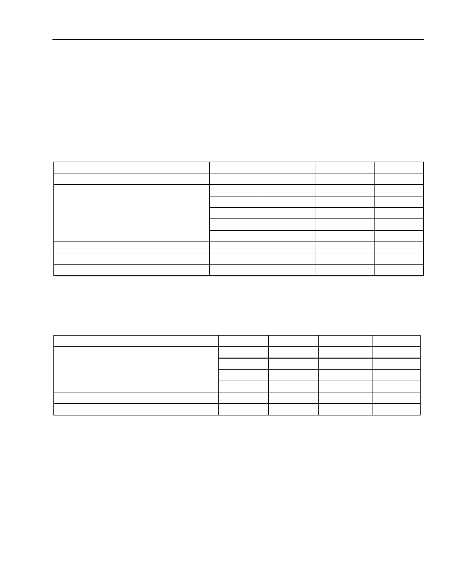
Agere Systems Inc.
55
Data Sheet
August 2001
Eight-Channel x 850 Mbits/s Backplane Transceiver
ORCA ORT8850 FPSC
Absolute Maximum Ratings
Stresses in excess of the absolute maximum ratings can cause permanent damage to the device. These are abso-
lute stress ratings only. Functional operation of the device is not implied at these or any other conditions in excess
of those given in the operations sections of this data sheet. Exposure to absolute maximum ratings for extended
periods can adversely affect device reliability.
The ORCA Series 3+ FPSCs include circuitry designed to protect the chips from damaging substrate injection cur-
rents and to prevent accumulations of static charge. Nevertheless, conventional precautions should be observed
during storage, handling, and use to avoid exposure to excessive electrical stress.
Table 13. Absolute Maximum Ratings
* V
DD
A_SHIM and V
DD
A_STM are analog power supply inputs which need to be isolated from other power supplies on the board.
Recommended Operating Conditions
Table 14. Recommended Operating Conditions
* For recommended operating conditions for V
DD
IO, see the Series 4 FPGA Data Sheet and the Series 4 I/O Buffer Application Note.
V
DD
A_SHIM and V
DD
A_STM are analog power supply inputs which need to be isolated from other power supplies on the board.
V
DD
33 is an analog power supply for the FPGA PLLs and needs to be isolated from other power supplies on the board.
Parameter
Symbol
Min
Max
Unit
Storage Temperature
T
stg
≠65 150 ∞C
Power Supply Voltage with Respect to Ground
V
DD
33
≠0.3
4.2
V
V
DD
IO
≠0.3
4.2
V
V
DD
15
≠0.3
2.0
V
V
DD
A_SHIM*
≠0.3
2.0
V
V
DD
A_STM*
≠0.3
2.0
V
Input Signal with Respect to Ground
--
≠0.3
V
DDIO
+ 0.3
V
Signal Applied to High-impedance Output
--
≠0.3
V
DDIO
+ 0.3
V
Maximum Package Body Temperature
--
--
220
∞C
Parameter
Symbol
Min
Max
Unit
Power Supply Voltage with Respect to Ground*
V
DD
33
2.7
3.6
V
V
DD
15
1.4
1.6
V
V
DD
A_SHIM
1.4
1.6
V
V
DD
A_STM
1.4
1.6
V
Input Voltages
V
IN
≠0.3
V
DDIO
+ 0.3
V
Junction Temperature
T
J
≠40
125
∞C
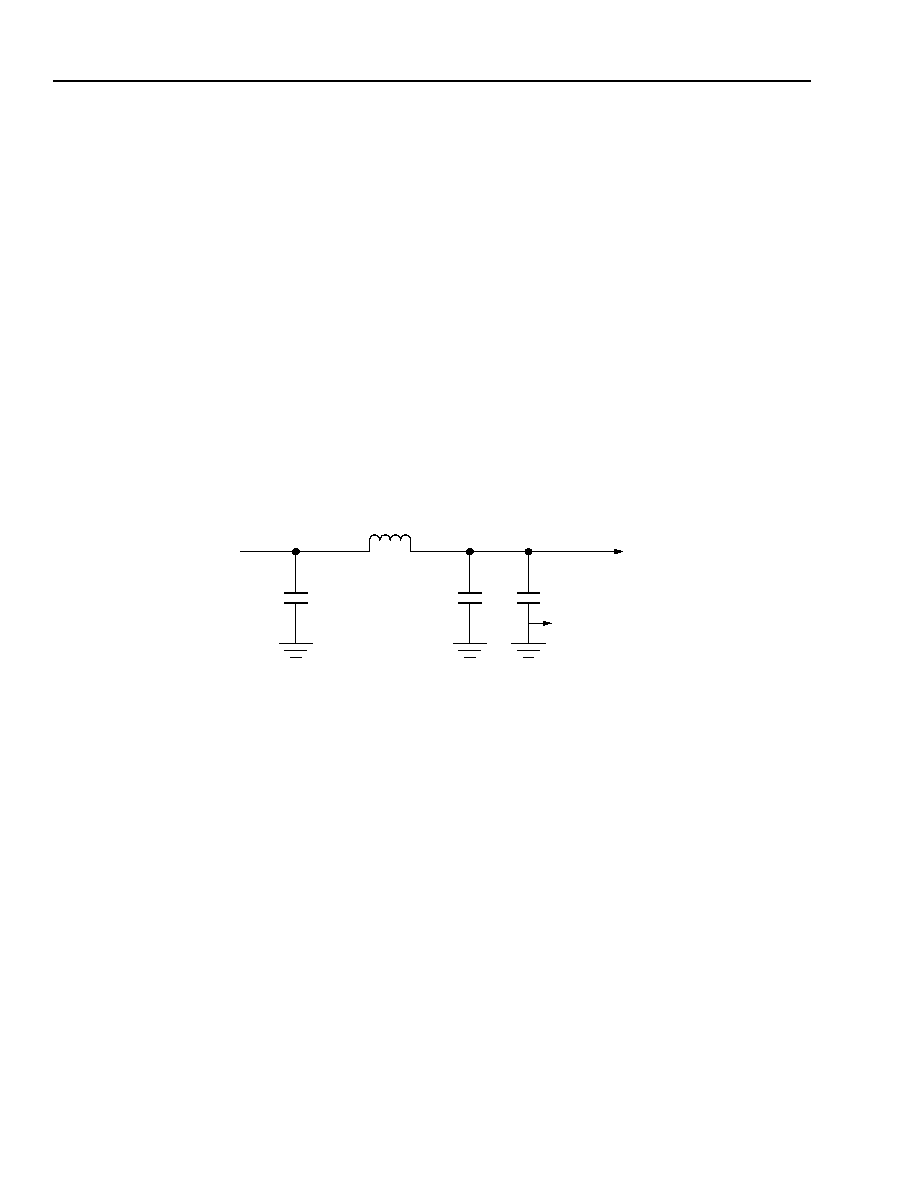
56
Agere Systems Inc.
Data Sheet
August 2001
Eight-Channel x 850 Mbits/s Backplane Transceiver
ORCA ORT8850 FPSC
Power Supply Decoupling LC Circuit
The 850 MHz HSI macro contains both analog and digital circuitry. The data recovery function, for example, is
implemented as primarily a digital function, but it relies on a conventional analog phase-locked loop to provide its
850 MHz reference frequency. The internal analog phase-locked loop contains a voltage-controlled oscillator. This
circuit will be sensitive to digital noise generated from the rapid switching transients associated with internal logic
gates and parasitic inductive elements. Generated noise that contains frequency components beyond the band-
width of the internal phase-locked loop (about 3 MHz) will not be attenuated by the phase-locked loop and will
impact bit error rate directly. Thus, separate power supply pins are provided for these critical analog circuit ele-
ments.
Additional power supply filtering in the form of a LC pi filter section will be used between the power supply source
and these device pins as shown in Figure 16. The corner frequency of the LC filter is chosen based on the power
supply switching frequency, which is between 100 kHz and 300 kHz in most applications.
Capacitors C1 and C2 are large electrolytic capacitors to provide the basic cut-off frequency of the LC filter. For
example, the cutoff frequency of the combination of these elements might fall between 5 kHz and 50 kHz. Capaci-
tor C3 is a smaller ceramic capacitor designed to provide a low-impedance path for a wide range of high-frequency
signals at the analog power supply pins of the device. The physical location of capacitor C3 must be as close to the
device lead as possible. Multiple instances of capacitors C3 can be used if necessary. The recommended filter for
the HSI macro is shown below: L = 4.7
µ
H, RL = 1
, C1 = 0.01
µ
F, C2 = 0.01
µ
F, C3 = 4.7
µ
F.
5-9344(F)
Figure 16. Sample Power Supply Filter Network for Analog HSI Power Supply Pins
The Rapid IO interface to Pi-Sched also has internal PLLs that require an analog supply, V
DD
A_SHIM. The same
power supply filter network shown above should be repeated and applied to the V
DD
A_SHIM inputs if this interface
is used. If both the Rapid IO interface and the HSI interface are used, two seperate copies of this interface should
be used.
If the programmable PLLs on the FPGA potrion of the device are to be used, then the V
DD
33 supply must isolated
in the same way. More information on this and other requirements for the FPGA PLLs can be found in the Series 4
PLL application note.
C2
+
C3
+
TO DEVICE
PLL_V
SSA
C1
+
FROM POWER
SUPPLY SOURCE
L
V
DDA
_STM
Agere Systems Inc.
57
Data Sheet
August 2001
Eight-Channel x 850 Mbits/s Backplane Transceiver
ORCA ORT8850 FPSC
HSI Electrical and Timing Characteristics
Table 15. Absolute Maximum Ratings
Table 16. Recommended Operating Conditions
Table 17. Receiver Specifications
* Scrambled data stream conforming to SONET STS-12 and SDH STM-4 data format using either a PN7 or PN9 sequence.
--PN7 characteristic is 1 + X
6
+ X
7
.
--PN9 characteristic is 1 + X
4
+ X
9
.
Alternatively 8B/10B encoded data is also valid input data.
This sequence should not occur more than once per minute.
Translates to a frequency change of 500 ppm.
ß A unit interval for 622.08 Mbits/s data is 1.6075 ns.
Table 18. Transmitter Specifications
Table 19. Synthesizer Specifications
* External 10 k
resistor to analog ground required.
Translates to a frequency change of 500 ppm.
Parameter
Conditions
Min
Typ
Max
Unit
Power Dissipation on V
DD
A_STM
Eight channels
--
--
385
mW
Parameter
Conditions
Min
Typ
Max
Unit
V
DD
15 Supply Voltage
--
1.4
--
1.6
V
Junction Temperature
T
J
≠40
--
125
∞C
Parameter
Conditions
Min
Typ
Max
Unit
Input Data*
Stream of Nontransitions
--
--
--
60
bits
Phase Change, Input Signal
Over a 200 ns time interval
--
--
100
ps
Eye Opening
ß
--
0.4
--
--
U
I
p-p
Jitter Tolerance
Jitter Tolerance:
250 kHz
25 kHz
2 kHz
--
--
--
--
--
--
--
0.6
6
60
U
I
p-p
U
I
p-p
U
I
p-p
Parameter
Conditions
Min
Typ
Max
Unit
Output Jitter, Generated
250 kHz to 5 MHz (measured
with a spectrum analyzer)
--
--
0.15
U
I
p-p
Output Jitter, Generated (including I/O buffers)
250 kHz to 5 MHz
--
--
0.25
U
I
p-p
Parameter
Conditions
Min
Typ
Max
Unit
PLL*
Loop Bandwidth
--
--
--
6
MHz
Jitter Peaking
--
--
--
2
dB
Powerup Reset Time
--
10
--
--
s
Lock Aquisition Time
--
--
--
1
ms
Input Reference Clock
Frequency
--
62.5
--
212.50
MHz
Frequency Deviation
--
--
--
100
ppm
Phase Change
Over a 200 ns time interval
--
--
100
ps
58
Agere Systems Inc.
Data Sheet
August 2001
Eight-Channel x 850 Mbits/s Backplane Transceiver
ORCA ORT8850 FPSC
Parallel RapidIO-like Interface Timing Characteristics
Figure 17 illustrates the timing for the receive parallel interfaces A, B, and C (DDR). The recommended operating
conditions for this interface are the same as for the HSI interface show in Table 16. Table 20 shows the worst case
timing parameters for this interface made under these conditions.
5-9085.c(F)
Figure 17. Receive Parallel Data/Control Timing
Table 20. Parallel Receive Data/Control Timing
Figure 18 illustrates the timing for the transmit parallel interfaces A, B, and C (DDR). The recommended operating
conditions for this interface are the same as for the HSI interface shown in Table 16. Table 21 shows the worst case
timing parameters for this interface under these conditions.
2289(F)
Figure 18. Transmit Parallel Data/Control Timing
Table 21. Transmit Parallel Data/Control Timing
Symbol
Parameter
≠1
≠2
≠3
Unit
Min
Max
Min
Max
Min
Max
t1
Clock Frequency
--
266
--
290
--
315
MHz
--
Clock Duty Cycle
40
60
40
60
40
60
%
--
Clock Rise/Fall Time
--
1.0
--
1.0
--
1.0
V/ns
t2
Data/Control Setup Time Required
290
--
270
--
260
--
ps
t3
Data/Control Hold Time Required
290
--
270
--
260
--
ps
Symbol
Parameter
≠1
≠2
≠3
Unit
Min
Max
Min
Max
Min
Max
t4
Clock Frequency
--
266
--
290
--
315
MHz
--
Clock Duty Cycle
45
55
45
55
45
55
%
--
Clock rise/Fall Time
--
1.0
--
1.0
--
1.0
V/ns
t5
Data Delay from Clock Edge
510
--
510
--
510
--
ps
RXCLK
RXSOC
P
N
P
N
t1
t3
t2
RXD[7:0]
TXCLK
TXSOC
P
N
P
N
t4
t5
TXD[7:0]
t5
t5
t5
t5
t5

Agere Systems Inc.
59
Data Sheet
August 2001
Eight-Channel x 850 Mbits/s Backplane Transceiver
ORCA ORT8850 FPSC
Embedded Core LVDS I/O
Table 22. Driver dc Data*
* V
DD
33 = 3.1 V--3.5 V, V
DD
15 = 1.4 V--1.6 V, ≠40 ∞C, and slow-fast process.
External reference, REF10 = 1.0 V ± 3%, REF14 = 1.4 V ± 3%.
Table 23. Driver ac Data*
* V
DD
33 = 3.1 V--3.5 V, V
DD
15 = 1.4 V--1.6 V, ≠40 ∞C, and slow-fast process.
Table 24. Driver Power Consumption*
* V
DD
33 = 3.1 V--3.5 V, V
DD
15 = 1.4 V--1.6 V, ≠40 ∞C, and slow-fast process.
Parameter
Symbol
Test Conditions
Min
Typ
Max
Unit
Output Voltage High, V
OA
or V
OB
V
OH
R
LOAD
= 100
± 1%
--
--
1.475
V
Output Voltage Low, V
OA
or V
OB
V
OL
R
LOAD
= 100
± 1%
0.925
--
--
V
Output Differential Voltage
V
OD
R
LOAD
= 100
± 1%
0.25
--
0.45
V
Output Offset Voltage
V
OS
R
LOAD
= 100
± 1%
1.125*
--
1.275
V
Output Impedance, Differential
R
o
V
CM
= 1.0 V and 1.4 V
80
100
120
R
O
Mismatch Between A and B
R
O
V
CM
= 1.0 V and 1.4 V
--
--
10
%
Change in Differential Voltage Between
Complementary States
V
OD
R
LOAD
= 100
± 1%
--
--
25
mV
Change in Output Offset Voltage
Between Complementary States
V
OS
R
LOAD
= 100
± 1%
--
--
25
mV
Output Current
I
SA,
I
SB
Driver shorted to GND
--
--
24
mA
Output Current
I
SAB
Drivers shorted together
--
--
12
mA
Power-off Output Leakage
|Ixa|, |Ixb|
V
DD
= 0 V
V
PAD
, V
PADN
= 0 V--2.5 V
--
--
10
mA
Parameter
Symbol
Test Conditions
Min
Typ
Max
Unit
V
OD
Fall Time, 80% to 20%
t
F
Z
L
= 100
± 1%
C
PAD
= 3.0 pF, C
PAD
= 3.0 pF
100
--
210
ps
V
OD
Rise Time, 20% to 80%
t
R
Z
L
= 100
± 1%
C
PAD
= 3.0 pF, C
PAD
= 3.0 pF
100
--
210
ps
Differential Skew
|t
PHLA
≠ t
PLHB
| or
|t
PHLB
≠ t
PLHA
|
t
SKEW1
Any differential pair on package at 50%
point of the transition
--
--
50
ps
Channel-to-channel Skew
|tpDIFFm ≠ tpDIFFn|,
t
SKEW2
Any two signals on package at 0 V
differential
--
--
--
ps
Propagation Delay Time
t
PLH
t
PHL
Z
L
= 100
± 1%
C
PAD
= 3.0 pF, C
PADN
= 3.0 pF
0.54
0.55
0.77
0.76
1.10
1.09
ns
ns
Parameter
Symbol
Test Conditions
Min
Max
Unit
Driver dc Power
PD
dc
Z
L
= 100
± 1%
--
26.0
mW
Driver ac Power
PD
ac
Z
L
= 100
± 1%
C
PAD
= 3.0 pF, C
PADN
= 3.0 pF
--
64
µ
W/
MHz

60
Agere Systems Inc.
Data Sheet
August 2001
Eight-Channel x 850 Mbits/s Backplane Transceiver
ORCA ORT8850 FPSC
Embedded Core LVDS I/O
(continued)
LVDS Receiver Buffer Requirements
Table 25. Receiver ac Data*
* V
DD
= 3.1 V--3.5 V, 0 ∞C --125 ∞C , slow-fast process.
Table 26. Receiver Power Consumption*
* V
DD
= 3.1 V--3.5 V, 0 ∞C --125 ∞C , slow-fast process.
Table 27. Receiver dc Data*
* V
DD
= 3.1 V--3.5 V, 0 ∞C --125 ∞C , slow-fast process.
Table 28. LVDS Operating Parameters
Note:Under worst-case operating condition, the LVDS driver will withstand a disabled or unpowered receiver for an unlimited period of time with-
out being damaged. Similarly, when outputs are short-circuited to each other or to ground, the LVDS will not suffer permanent damage.
The LVDS driver supports hot insertion. Under a well-controlled environment, the LVDS I/O can drive backplane as well as cable.
Parameter
Symbol
Test Conditions
Min
Max
Unit
Pulse-width Distortion
t
pwd
V
IDTH
= 100 mV, 450 MHz
--
160
ps
Propagation Delay Time
t
PLH
t
PHL
C
L
= 0.5 pF
0.60
0.60
1.41
1.47
ns
ns
With Common-mode Variation (0 V to 2.4 V)
t
PD
C
L
= 0.5 pF
--
50
ps
Output Rise Time, 20% to 80%
t
R
C
L
= 0.5 pF
150
350
ps
Output Fall Time, 80% to 20%
t
F
C
L
= 0.5 pF
150
350
ps
Parameter
Symbol
Test Conditions
Min
Max
Unit
Receiver dc Power
P
Rdc
dc
--
20.4
mW
Receiver ac Power
P
Rac
ac
C
L
= 0.5 pF
--
4.5
µ
W/
MHz
Parameter
Symbol
Test Conditions
Min
Typ
Max
Unit
Input Voltage Range, VIA or VIB
V
I
V
GPD
< 925 mV
dc ≠ 1 MHz
0.0
1.2
2.4
V
Input Differential Threshold
V
IDTH
V
GPD
< 925 mV
450 MHz
≠100
--
100
mV
Input Differential Hysteresis
V
HYST
(+V
IDTHH
) ≠ (≠V
IDTHL
)
--
--
--
mV
Receiver Differential Input Impedance
R
IN
With build-in termination,
center-tapped
80
100
120
Parameter
Test Conditions
Min
Normal
Max
Unit
Transmit Termination Resistor
--
80
100
120
Receiver Termination Resistor
--
80
100
120
Temperature Range
--
≠40
--
125
∞C
Power Supply V
DD
33
--
3.1
--
3.5
V
Power Supply V
DD
15
--
1.4
--
1.6
V
Power Supply V
SS
--
--
0
--
V
Agere Systems Inc.
61
Data Sheet
August 2001
Eight-Channel x 850 Mbits/s Backplane Transceiver
ORCA ORT8850 FPSC
Input/Output Buffer Measurement Conditions (on-LVDS Buffer)
Note: Switch to V
DD
for
T
PLZ
/T
PZL
; switch to GND for T
PHZ
/T
PZH
.
5-3234(F)
Figure 19. ac Test Loads
5-3233.a(F)
Figure 20. Output Buffer Delays
5-3235(F)
Figure 21. Input Buffer Delays
50 pF
A. Load Used to Measure Propagation Delay
TO THE OUTPUT UNDER TEST
TO THE OUTPUT UNDER TEST
50 pF
V
CC
GND
1 k
B. Load Used to Measure Rising/Falling Edges
V
DD
T
PHH
V
DD
/2
V
SS
out[i]
PAD
OUT
1.5 V
0.0 V
T
PLL
PAD
out[i]
ac TEST LOADS (SHOWN ABOVE)
ts[i]
OUT
0.0 V
1.5 V
T
PHH
T
PLL
PAD
in[i]
IN
3.0 V
V
SS
V
DD
/2
V
DD
PAD IN
in[i]
62
Agere Systems Inc.
Data Sheet
August 2001
Eight-Channel x 850 Mbits/s Backplane Transceiver
ORCA ORT8850 FPSC
LVDS Buffer Characteristics
Termination Resistor
The LVDS drivers and receivers operate on a 100
differential impedance, as shown below. External resistors are
not required. The differential driver and receiver buffers include termination resistors inside the device package, as
shown in Figure 22 below.
5-8703(F)
Figure 22. LVDS Driver and Receiver and Associated Internal Components
LVDS Driver Buffer Capabilities
Under worst-case operating condition, the LVDS driver must withstand a disabled or unpowered receiver for an
unlimited period of time without being damaged. Similarly, when its outputs are short-circuited to each other or to
ground, the LVDS driver will not suffer permanent damage. Figure 23 illustrates the terms associated with LVDS
driver and receiver pairs.
5-8704(F)
Figure 23. LVDS Driver and Receiver
5-8705(F)
Figure 24. LVDS Driver
LVDS DRIVER
50
50
LVDS RECEIVER
CENTER TAP
DEVICE PINS
100
EXTERNAL
V
GPD
V
OA
V
OB
V
IA
V
IB
A
B
AA
BB
DRIVER INTERCONNECT
RECEIVER
V
OA
A
V
OB
B
C
A
C
B
R
LOAD
V
OD
= (V
OA
≠ V
OB
)
V
Agere Systems Inc.
63
Data Sheet
August 2001
Eight-Channel x 850 Mbits/s Backplane Transceiver
ORCA ORT8850 FPSC
Pin Information
This section describes the pins and signals that perform FPGA-related functions. During configuration, the user-
programmable I/Os are 3-stated and pulled up with an internal resistor. If any FPGA function pin is not used (or not
bonded to package pin), it is also 3-stated and pulled up after configuration.
Table 29
.
FPGA Common-Function Pin Description
Symbol
I/O
Description
Dedicated Pins
V
DD
33
-- 3 V positive power supply.
V
DD
15
-- 1.5 V positive power supply for internal logic.
V
DDIO
-- Positive power supply used by I/O banks.
GND
-- Ground supply.
PTEMP
I
Temperature sensing diode pin. Dedicated input.
RESET
I
During configuration,
RESET
forces the restart of configuration and a pull-up is enabled.
After configuration,
RESET
can be used as a general FPGA input or as a direct input,
which causes all PLC latches/FFs to be asynchronously set/reset.
CCLK
I
O
In the master and asynchronous peripheral modes, CCLK is an output which strobes con-
figuration data in. In the slave or readback after configuration, CCLK is input synchronous
with the data on DIN or D[7:0]. CCLK is an output for daisy-chain operation when the lead
device is in master, peripheral, or system bus modes.
DONE
I
As an input, a low level on DONE delays FPGA start up after configuration.*
O
As an active-high, open-drain output, a high level on this signal indicates that configura-
tion is complete. DONE has an optional pull-up resistor.
PRGM
I
PRGM
is an active-low input that forces the restart of configuration and resets the bound-
ary scan circuitry. This pin always has an active pull-up.
RD_CFG
I
This pin must be held high during device initialization until the
INIT
pin goes high. This pin
always has an active pull-up.
During configuration,
RD_CFG
is an active-low input that activates the TS_ALL function
and 3-states all of the I/O.
After configuration,
RD_CFG
can be selected (via a bit stream option) to activate the
TS_ALL function as described above, or, if readback is enabled via a bit stream option, a
high-to-low transition on
RD_CFG
will initiate readback of the configuration data, including
PFU output states, starting with frame address 0.
RD_DATA/TDO
O
RD_DATA/TDO is a dual-function pin. If used for readback, RD_DATA provides configu-
ration data out. If used in boundary scan, TDO is test data out.
CFG_IRQ/MPI_IRQ
O
During JTAG, slave, master, and asynchronous peripheral configuration assertion on this
CFG_IRQ
(active-low) indicates an error or errors for block RAM or FPSC initialization.
MPI
active-low interrupt request output.
* The FPGA States of Operation section contains more information on how to control these signals during start up. The timing of DONE release
is controlled by one set of bit stream options, and the timing of the simultaneous release of all other configuration pins (and the activation of all
user I/Os) is controlled by a second set of options.
64
Agere Systems Inc.
Data Sheet
August 2001
Eight-Channel x 850 Mbits/s Backplane Transceiver
ORCA ORT8850 FPSC
Pin Information
(continued)
Table 29. FPGA Common-Function Pin Description (continued)
Symbol
I/O
Description
Special-Purpose Pins (Can also be used as a general I/O.)
M[3:0]
I
During powerup and initialization, M0--M3 are used to select the configuration mode with
their values latched on the rising edge of INIT. During configuration, a pull-up is enabled.
I/O After configuration, these pins are user-programmable I/O.*
PLL_CK[0:7]
I/O Dedicated PCM clock pins. These pins are a user-programmable I/O pins if not used by
PLLs.
P[TBTR]CLK[1:0][
TC]
I/O Pins dedicated for the primary clock. Input pins on the middle of each side with differential
pairing. They may be used as general I/O pins if not needed for clocking purposes.
TDI, TCK, TMS
I
If boundary scan is used, these pins are test data in, test clock, and test mode select inputs.
If boundary scan is not selected, all boundary scan functions are inhibited once configura-
tion is complete. Even if boundary scan is not used, either TCK or TMS must be held at
logic 1 during configuration. Each pin has a pull-up enabled during configuration.
I/O After configuration, these pins are user-programmable I/O.*
RDY/BUSY/RCLK
O
During configuration in peripheral mode, RDY/RCLK indicates another byte can be written
to the FPGA. If a read operation is done when the device is selected, the same status is
also available on D7 in asynchronous peripheral mode.
After configuration, if the MPI is not used, this pin is a user-programmable I/O pin.*
I/O During the master parallel configuration mode, RCLK is a read output signal to an external
memory. This output is not normally used.
HDC
O
High during configuration is output high until configuration is complete. It is used as a con-
trol output, indicating that configuration is not complete.
I/O After configuration, this pin is a user-programmable I/O pin.*
LDC
O
Low during configuration is output low until configuration is complete. It is used as a control
output, indicating that configuration is not complete.
I/O After configuration, this pin is a user-programmable I/O pin.*
INIT
I/O INIT is a bidirectional signal before and during configuration. During configuration, a pull-up
is enabled, but an external pull-up resistor is recommended. As an active-low, open-drain
output, INIT is held low during power stabilization and internal clearing of memory. As an
active-low input, INIT holds the FPGA in the wait-state before the start of configuration.
After configuration, this pin is a user-programmable I/O pin.*
CS0, CS1
I
CS0 and CS1 are used in the asynchronous peripheral, slave parallel, and microprocessor
configuration modes. The FPGA is selected when CS0 is low and CS1 is high. During con-
figuration, a pull-up is enabled.
I/O After configuration, these pins are user-programmable I/O pins.*
RD/MPI_STRB
I
RD is used in the asynchronous peripheral configuration mode. A low on RD changes D7
into a status output. As a status indication, a high indicates ready, and a low indicates busy.
WR and RD should not be used simultaneously. If they are, the write strobe overrides.
This pin is also used as the MPI data transfer strobe.
I/O After configuration, if the MPI is not used, this pin is a user-programmable I/O pin.*
* The FPGA States of Operation section contains more information on how to control these signals during start up. The timing of DONE
release is controlled by one set of bit stream options, and the timing of the simultaneous release of all other configuration pins (and the acti-
vation of all user I/Os) is controlled by a second set of options.

Agere Systems Inc.
65
Data Sheet
August 2001
Eight-Channel x 850 Mbits/s Backplane Transceiver
ORCA ORT8850 FPSC
Pin Information
(continued)
Table 29. FPGA Common-Function Pin Description (continued)
Symbol
I/O
Description
A[0:17]
MPI_BURST
MPI_BDIP
MPI_TSZ[1:0]
I
During MPI mode, the A[0:17] are used as the address bus driven by the PowerPC bus
master, utilizing the least significant bits of the PowerPC 32-bit address.
O
During master parallel configuration mode, A[0:17] address the configuration EPROM. In
MPI mode, many of the A[n] pins have alternate uses as described below. See the special
function blocks section for more MPI information. During configuration, if not in master
parallel or an MPI configuration mode, these pins are 3-stated with a pull-up enabled.
It is driven low to indicate a burst transfer is in progress. Driven high indicates that the
current transfer is not a burst.
It is driven by the PowerPC processor assertion of this pin indicates that the second beat
in front of the current one is requested by the master. Negated before the burst transfer
ends to abort the burst data phase.
MPI_TSZ[1:0] signals and are driven by the bus master to indicate the data transfer size
for the transaction. Set 10 for byte, 01 for half-word, and 00 for word.
If not used for MPI, these pins are user-programmable I/O pins.*
MPI_ACK
O
In PowerPC mode MPI operation, this is driven low indicating the MPI received the data
on the write cycle or returned data on a read cycle.
MPI_CLK
I
This is the PowerPC synchronous, positive-edge bus clock used for the MPI interface. It
can be a source of the clock for the embedded system bus. If MPI is used, this can be the
AMBA bus clock.
MPI_TEA
O
A low on the MPI transfer error acknowledge indicates that the MPI detects a bus error on
the internal system bus for the current transaction.
MPI_RTRY
O
This pin requests that the MPC860 relinquish the bus and retry the cycle.
D[0:31]
I/O Selectable data bus width from 8-, 16-, 32-bit. Driven by the bus master in a write transac-
tion. Driven by MPI in a read transaction.
I
D[0:7] receive configuration data during master parallel, peripheral, and slave parallel
configuration modes and each pin has a pull-up enabled. During serial configuration
modes, D0 is the DIN input.
D[7:3] output internal status for asynchronous peripheral mode when RD is low.
After configuration, the pins are user-programmable I/O pins.*
DP[3:0]
I/O Selectable parity bus width from 1, 2, 4-bit, DP[0] for D[0:7], DP[1] for D[8:15], DP[2] for
D[16:23], and DP[3] for D[24:32].
After configuration, this pin is a user-programmable I/O pin.*
DIN
I
During slave serial or master serial configuration modes, DIN accepts serial configuration
data synchronous with CCLK. During parallel configuration modes, DIN is the D0 input.
During configuration, a pull-up is enabled.
I/O After configuration, this pin is a user-programmable I/O pin.*
DOUT
O
During configuration, DOUT is the serial data output that can drive the DIN of daisy-
chained slave devices. Data out on DOUT changes on the rising edge of CCLK.
I/O After configuration, DOUT is a user-programmable I/O pin.*
* The FPGA States of Operation section contains more information on how to control these signals during start up. The timing of DONE
release is controlled by one set of bit stream options, and the timing of the simultaneous release of all other configuration pins (and the acti-
vation of all user I/Os) is controlled by a second set of options.

66
Agere Systems Inc.
Data Sheet
August 2001
Eight-Channel x 850 Mbits/s Backplane Transceiver
ORCA ORT8850 FPSC
Pin Information
(continued)
This section describes device I/O signals to/from the embedded core excluding the signals at the CIC boundary.
Table 30. FPSC Function Pin Description
* The V
SS
A_STM is combimed with V
SS
in packages that contain an internal V
SS
plane.
Symbol
I/O
Description
HSI LVDS Receive Pins
rxd_b_p0
I
LVDS work link--channel AA (shared with RapidIO port B) .
rxd_b_n0
I
LVDS work link--channel AA (shared with RapidIO port B).
rxd_c_p0
I
LVDS protect link--channel AA (shared with RapidIO port C).
rxd_c_n0
I
LVDS protect link--channel AA (shared with RapidIO port C).
rxd_b_p1
I
LVDS work link--channel AB (shared with RapidIO port B).
rxd_b_n1
I
LVDS work link--channel AB (shared with RapidIO port B).
rxd_c_p1
I
LVDS protect link--channel AB (shared with RapidIO port C).
rxd_c_n1
I
LVDS protect link--channel AB (shared with RapidIO port C).
rxd_b_p2
I
LVDS work link--channel AC (shared with RapidIO port B).
rxd_b_n2
I
LVDS work link--channel AC (shared with RapidIO port B).
rxd_c_p2
I
LVDS protect link--channel AC (shared with RapidIO port C).
rxd_c_n2
I
LVDS protect link--channel AC (shared with RapidIO port C).
rxd_b_p3
I
LVDS work link--channel AD (shared with RapidIO port B).
rxd_b_n3
I
LVDS work link--channel AD (shared with RapidIO port B).
rxd_c_p3
I
LVDS protect link--channel AD (shared with RapidIO port C).
rxd_c_n3
I
LVDS protect link--channel AD (shared with RapidIO port C).
rxd_b_p4
I
LVDS work link--channel BA (shared with RapidIO port B).
rxd_b_n4
I
LVDS work link--channel BA (shared with RapidIO port B).
rxd_c_p4
I
LVDS protect link--channel BA (shared with RapidIO port C).
rxd_c_n4
I
LVDS protect link--channel BA (shared with RapidIO port C).
rxd_b_p5
I
LVDS work link--channel BB (shared with RapidIO port B).
rxd_b_n5
I
LVDS work link--channel BB (shared with RapidIO port B).
rxd_c_p5
I
LVDS protect link--channel BB (shared with RapidIO port C).
rxd_c_n5
I
LVDS protect link--channel BB (shared with RapidIO port C).
rxd_b_p6
I
LVDS work link--channel BC (shared with RapidIO port B).
rxd_b_n6
I
LVDS work link--channel BC (shared with RapidIO port B).
rxd_c_p6
I
LVDS protect link--channel BC (shared with RapidIO port C).
rxd_c_n6
I
LVDS protect link--channel BC (shared with RapidIO port C).
rxd_b_p7
I
LVDS work link--channel BD (shared with RapidIO port B).
rxd_b_n7
I
LVDS work link--channel BD (shared with RapidIO port B).
rxd_c_p7
I
LVDS protect link--channel BD (shared with RapidIO port C).
rxd_c_n7
I
LVDS protect link--channel BD (shared with RapidIO port C).
DAUTREC
I
Disable auto recovery for the PLL. Internal pull-down.
V
DDA
_STM
I
Analog V
DD
1.5 V power supply for the HSI block.
V
SSA
_STM*
I
Analog V
SS
for the HSI block.

Agere Systems Inc.
67
Data Sheet
August 2001
Eight-Channel x 850 Mbits/s Backplane Transceiver
ORCA ORT8850 FPSC
Pin Information
(continued)
Table 30. FPSC Function Pin Description (continued)
Symbol
I/O
Description
HSI LVDS Transmit Pins
txd_b_p0
I
LVDS work link--channel AA (shared with RapidIO port B).
txd_b_n0
I
LVDS work link--channel AA (shared with RapidIO port B).
txd_c_p0
I
LVDS protect link--channel AA (shared with RapidIO port C).
txd_c_n0
I
LVDS protect link--channel AA (shared with RapidIO port C).
txd_b_p1
I
LVDS work link--channel AB (shared with RapidIO port B).
txd_b_n1
I
LVDS work link--channel AB (shared with RapidIO port B).
txd_c_p1
I
LVDS protect link--channel AB (shared with RapidIO port C).
txd_c_n1
I
LVDS protect link--channel AB (shared with RapidIO port C).
txd_b_p2
I
LVDS work link--channel AC (shared with RapidIO port B).
txd_b_n2
I
LVDS work link--channel AC (shared with RapidIO port B).
txd_c_p2
I
LVDS protect link--channel AC (shared with RapidIO port C).
txd_c_n2
I
LVDS protect link--channel AC (shared with RapidIO port C).
txd_b_p3
I
LVDS work link--channel AD (shared with RapidIO port B).
txd_b_n3
I
LVDS work link--channel AD (shared with RapidIO port B).
txd_c_p3
I
LVDS protect link--channel AD (shared with RapidIO port C).
txd_c_n3
I
LVDS protect link--channel AD (shared with RapidIO port C).
txd_b_p4
I
LVDS work link--channel BA (shared with RapidIO port B).
txd_b_n4
I
LVDS work link--channel BA (shared with RapidIO port B).
txd_c_p4
I
LVDS protect link--channel BA (shared with RapidIO port C).
txd_c_n4
I
LVDS protect link--channel BA (shared with RapidIO port C).
txd_b_p5
I
LVDS work link--channel BB (shared with RapidIO port B).
txd_b_n5
I
LVDS work link--channel BB (shared with RapidIO port B).
txd_c_p5
I
LVDS protect link--channel BB (shared with RapidIO port C).
txd_c_n5
I
LVDS protect link--channel BB (shared with RapidIO port C).
txd_b_p6
I
LVDS work link--channel BC (shared with RapidIO port B).
txd_b_n6
I
LVDS work link--channel BC (shared with RapidIO port B).
txd_c_p6
I
LVDS protect link--channel BC (shared with RapidIO port C).
txd_c_n6
I
LVDS protect link--channel BC (shared with RapidIO port C).
txd_b_p7
I
LVDS work link--channel BD (shared with RapidIO port B).
txd_b_n7
I
LVDS work link--channel BD (shared with RapidIO port B).
txd_c_p7
I
LVDS protect link--channel BD (shared with RapidIO port C).
txd_c_n7
I
LVDS protect link--channel BD (shared with RapidIO port C).

68
Agere Systems Inc.
Data Sheet
August 2001
Eight-Channel x 850 Mbits/s Backplane Transceiver
ORCA ORT8850 FPSC
Pin Information
(continued)
Table 30. FPSC Function Pin Description (continued)
* The V
SS
A_shim is combimed with V
SS
in packages that contain an internal V
SS
plane.
Symbol
I/O
Description
HSI Test Signals
tstclk
I
Test clock for emulation of 622 MHz clock during PLL bypass. Internal pull-down.
mreset
I
Test mode reset. Internal pull-down.
testrst
I
Resets receiver clock division counter. Internal pull-up.
resettx
I
Resets transmitter clock division counter. Internal pull-up.
tstMUX[9:0]s
O
Test mode output port.
scan_tstmd
I
Test mode enable. Must be tie-low for normal operation.
scan_en
I
Scan test enable. Internal pull-up.
tstsuftld
I
Internal pull-down.
e_toggle
I
Internal pull-down.
elsel
I
Internal pull-down.
exdnup
I
Internal pull-down.
RapidIO LVDS Interface Pins (Receiver)
rxd_a_p<7:0>
I
LVDS data for RapidIO, receiver port A.
rxd_a_n<7:0>
I
LVDS data for RapidIO, receiver port A.
rxsoc_a_p
I
LVDS start-of-cell for RapidIO, receiver port A.
rxsoc_a_n
I
LVDS start-of-cell for RapidIO, receiver port A.
rxclk_a_p
I
LVDS receive clock for RapidIO, receiver port A.
rxclk_a_n
I
LVDS receive clock for RapidIO, receiver port A.
lvctap_a<1:0>
--
LVDS input center tap (use 0.01 uF to GND) internal pull-up.
rxd_b_p<7:0>
I
LVDS data for RapidIO, receiver port B.
rxd_b_n<7:0>
I
LVDS data for RapidIO, receiver port B.
rxsoc_b_p
I
LVDS start-of-cell for RapidIO, receiver port B.
rxsoc_b_n
I
LVDS start-of-cell for RapidIO, receiver port B.
rxclk_b_p
I
LVDS receive clock for RapidIO, receiver port B.
rxclk_b_n
I
LVDS receive clock for RapidIO, receiver port B.
lvctap_b<4:0>
--
LVDS input center tap (use 0.01 µF to GND) internal pull-up.
rxd_c_p<7:0>
I
LVDS data for RapidIO, receiver port C.
rxd_c_n<7:0>
I
LVDS data for RapidIO, receiver port C.
rxsoc_c_p
I
LVDS start-of-cell for RapidIO, receiver port C.
rxsoc_c_n
I
LVDS start-of-cell for RapidIO, receiver port C.
rxclk_c_p
I
LVDS receive clock for RapidIO, receiver port C.
rxclk_c_n
I
LVDS receive clock for RapidIO, receiver port C.
lvctap_c<4:0>
--
LVDS input center tap (use 0.01 µF to GND) internal pull-up.
ref10
--
LVDS reference voltage: 1.0 V ± 3%.
ref14
--
LVDS reference voltage: 1.4 V ± 3%.
reshi
--
LVDS resistor high pin ( 100
in series with reslo).
reslo
--
LVDS resistor low pin ( 100
in series with reshi).
V
DD
A_shim
I
Analog V
DD
1.5 V power supply for the Rapid IO block.
V
SS
A_shim
I
Analog V
SS
for the Rapid IO block.

Agere Systems Inc.
69
Data Sheet
August 2001
Eight-Channel x 850 Mbits/s Backplane Transceiver
ORCA ORT8850 FPSC
Pin Information
(continued)
Table 30. FPSC Function Pin Description (continued)
Symbol
I/O
Description
RapidIO LVDS Interface Pins (Transmitter)
txd_a_p<7:0>
O
LVDS data for RapidIO, transmitter port A.
txd_a_n<7:0>
O
LVDS data for RapidIO, transmitter port A.
txsoc_a_p
O
LVDS start-of-cell for RapidIO, transmitter port A.
txsoc_a_n
O
LVDS start-of-cell for RapidIO, transmitter port A.
txclk_a_p
O
LVDS receive clock for RapidIO, transmitter port A.
txclk_a_n
O
LVDS receive clock for RapidIO, transmitter port A.
txd_b_p<7:0>
O
LVDS data for RapidIO, transmitter port B.
txd_b_n<7:0>
O
LVDS data for RapidIO, transmitter port B.
txsoc_b_p
O
LVDS start-of-cell for RapidIO, transmitter port B.
txsoc_b_n
O
LVDS start-of-cell for RapidIO, transmitter port B.
txclk_b_p
O
LVDS receive clock for RapidIO, transmitter port B.
txclk_b_n
O
LVDS receive clock for RapidIO, transmitter port B.
txd_c_p<7:0>
O
LVDS data for RapidIO, transmitter port C.
txd_c_n<7:0>
O
LVDS data for RapidIO, transmitter port C.
txsoc_c_p
O
LVDS start-of-cell for RapidIO, transmitter port C.
txsoc_c_n
O
LVDS start-of-cell for RapidIO, transmitter port C.
txclk_c_p
O
LVDS receive clock for RapidIO, transmitter port C.
txclk_c_n
O
LVDS receive clock for RapidIO, transmitter port C.
MISC System Signals
rst_n
I
Reset the core only. The FPGA logic is not reset by rst_n.
Internal pull down allows chip to stay in reset state when external driver
loses power.
sys_clk_p
I
LVDS system clock, 50% duty cycle, also the reference clock of PLL.
sys_clk_n
I
LVDS system clock, 50% duty cycle, also the reference clock of PLL.
gclk_p
I
LVDS clock for RapidIO PLL internal pull-up.
gclk_n
I
LVDS clock for RapidIO PLL internal pull-up.
dxp
--
Temperature-sensing diode (anode +).
dxn
--
Temperature-sensing diode (cathode ≠).
lvctap_sk
O
LVDS center-tap for sys_clk (use 0.01 µf to GND).
lvctap_gk
O
LVDS center-tap for gclk (use 0.01 µf to GND).

70
Agere Systems Inc.
Data Sheet
August 2001
Eight-Channel x 850 Mbits/s Backplane Transceiver
ORCA ORT8850 FPSC
Pin Information
(continued)
In
Table 31, an input refers to a signal flowing into the embedded core and an output refers to a signal flowing out
of the embedded core.
Table 31. Embedded Core/FPGA Interface Signal Description
Pin Name
I/O
Description
STM or 8B/10B Signals
dinaa<7:0>
I
Parallel bus of STM slice A, transmitter A. MSB is bit 7.
dinaa_par
I
Parity for STM slice A, transmitter A.
dinaa_fp
I
Frame pulse or K control for STM slice A, transmitter A.
dinab<7:0>
I
Parallel bus of STM slice A, transmitter B. MSB is bit 7.
dinab_par
I
Parity for STM slice A, transmitter B.
dinab_fp
I
Frame pulse or K control for STM slice A, transmitter B.
dinac<7:0>
I
Parallel bus of STM slice A, transmitter C. MSB is bit 7.
dinac_par
I
Parity for STM slice A, transmitter C.
dinac_fp
I
Frame pulse or K control for STM slice A, transmitter C.
dinad<7:0>
I
Parallel bus of STM slice A, transmitter D. MSB is bit 7.
dinad_par
I
Parity for STM slice A, transmitter D.
dinad_fp
I
Frame pulse or K control for STM slice A, transmitter D.
dinba<7:0>
I
Parallel bus of STM slice B, transmitter A. MSB is bit 7.
dinba_par
I
Parity for STM slice B, transmitter A.
dinba_fp
I
Frame pulse or K control for STM slice B, transmitter A.
dinbb<7:0>
I
Parallel bus of STM slice B, transmitter B. MSB is bit 7.
dinbb_par
I
Parity for STM slice B, transmitter B.
dinbb_fp
I
Frame pulse or K control for STM slice B, transmitter B.
dinbc<7:0>
I
Parallel bus of STM slice B, transmitter C. MSB is bit 7.
dinbc_par
I
Parity for STM slice B, transmitter C.
dinbc_fp
I
Frame pulse or K control for STM slice B, transmitter C.
dinbd<7:0>
I
Parallel bus of STM slice B, transmitter D. MSB is bit 7.
dinbd_par
I
Parity for STM slice B, transmitter D.
dinbd_fp
I
Frame pulse or K control for STM slice B, transmitter D.
doutaa<7:0>
O
Parallel bus of STM slice A, receiver A. MSB is bit 7.
doutaa_par
O
Parity for parallel bus of STM slice A, receiver A.
doutaa_spe
O
SPE signal for parallel bus of STM slice A, receiver A.
doutaa_c1j1
O
C1J1 signal for parallel bus of STM slice A, receiver A.
doutaa_en
O
Enable for parallel bus of STM slice A, receiver A.
doutaa_fp
O
Frame pulse or COMMADET for parallel bus of STM slice A, receiver A.
doutab<7:0>
O
Parallel bus of STM slice A, receiver B. MSB is bit 7.
doutab_par
O
Parity for parallel bus of STM slice A, receiver B.
doutab_spe
O
SPE signal for parallel bus of STM slice A, receiver B.
doutab_c1j1
O
C1J1 signal for parallel bus of STM slice A, receiver B.
doutab_en
O
Enable for parallel bus of STM slice A, receiver B.
doutab_fp
O
Frame pulse or COMMADET for parallel bus of STM slice A, receiver B.

Agere Systems Inc.
71
Data Sheet
August 2001
Eight-Channel x 850 Mbits/s Backplane Transceiver
ORCA ORT8850 FPSC
Pin Information
(continued)
Table 31. Embedded Core/FPGA Interface Signal Description (continued)
Pin Name
I/O
Description
STM or 8B/10B Signals (continued)
doutac<7:0>
O
Parallel bus of STM slice A, receiver C. MSB is bit 7.
doutac_par
O
Parity for parallel bus of STM slice A, receiver C.
doutac_spe
O
SPE signal for parallel bus of STM slice A, receiver C.
doutac_c1j1
O
C1J1 signal for parallel bus of STM slice A, receiver C.
doutac_en
O
Enable for parallel bus of STM slice A, receiver C.
doutac_fp
O
Frame pulse or COMMADET for parallel bus of STM slice A, receiver C.
doutad<7:0>
O
Parallel bus of STM slice A, receiver D. MSB is bit 7.
doutad_par
O
Parity for parallel bus of STM slice A, receiver D.
doutad_spe
O
SPE signal for parallel bus of STM slice A, receiver D.
doutad_c1j1
O
C1J1 signal for parallel bus of STM slice A, receiver D.
doutad_en
O
Enable for parallel bus of STM slice A, receiver D.
doutad_fp
O
Frame pulse or COMMADET for parallel bus of STM slice A, receiver D.
doutba<7:0>
O
Parallel bus of STM slice B, receiver A. MSB is bit 7.
doutba_par
O
Parity for parallel bus of STM slice B, receiver A.
doutba_spe
O
SPE signal for parallel bus of STM slice B, receiver A.
doutba_c1j1
O
C1J1 signal for parallel bus of STM slice B, receiver A.
doutba_en
O
Enable for parallel bus of STM slice B, receiver A.
doutba_fp
O
Frame pulse or COMMADET for parallel bus of STM slice B, receiver A.
doutbb<7:0>
O
Parallel bus of STM slice B, receiver B. MSB is bit 7.
doutbb_par
O
Parity for parallel bus of STM slice B, receiver B.
doutbb_spe
O
SPE signal for parallel bus of STM slice B, receiver B.
doutbb_c1j1
O
C1J1 signal for parallel bus of STM slice B, receiver B.
doutbb_en
O
Enable for parallel bus of STM slice B, receiver B.
doutbb_fp
O
Frame pulse or COMMADET for parallel bus of STM slice B, receiver B.
doutbc<7:0>
O
Parallel bus of STM slice B, receiver C. MSB is bit 7.
doutbc_par
O
Parity for parallel bus of STM slice B, receiver C.
doutbc_spe
O
SPE signal for parallel bus of STM slice B, receiver C.
doutbc_c1j1
O
C1J1 signal for parallel bus of STM slice B, receiver C.
doutbc_en
O
Enable for parallel bus of STM slice B, receiver C.
doutbc_fp
O
Frame pulse or COMMADET for parallel bus of STM slice B, receiver C.
doutbd<7:0>
O
Parallel bus of STM slice B, receiver D. MSB is bit 7.
doutbd_par
O
Parity for parallel bus of STM slice B, receiver D.
doutbd_spe
O
SPE signal for parallel bus of STM slice B, receiver D.
doutbd_c1j1
O
C1J1 signal for parallel bus of STM slice B, receiver D.
doutbd_en
O
Enable for parallel bus of STM slice B, receiver D.
doutbd_fp
O
Frame pulse or COMMADET for parallel bus of STM slice B, receiver D.

72
Agere Systems Inc.
Data Sheet
August 2001
Eight-Channel x 850 Mbits/s Backplane Transceiver
ORCA ORT8850 FPSC
Pin Information
(continued)
Table 31. Embedded Core/FPGA Interface Signal Description (continued)
Pin Name
I/O
Description
TOH Signals
toh_clk
I
TX and RX TOH serial links clock (25 MHz to 77.76 MHz).
toh_inaa
I
TOH serial link for STM slice A, transmitter A.
toh_inab
I
TOH serial link for STM slice A, transmitter B.
toh_inac
I
TOH serial link for STM slice A, transmitter C.
toh_inad
I
TOH serial link for STM slice A, transmitter D.
toh_inba
I
TOH serial link for STM slice B, transmitter A.
toh_inbb
I
TOH serial link for STM slice B, transmitter B.
toh_inbc
I
TOH serial link for STM slice B, transmitter C.
toh_inbd
I
TOH serial link for STM slice B, transmitter D.
tx_toh_ck_en
I
TX TOH serial link clock enable.
toh_outaa
O
TOH serial link for STM slice A, receiver A.
toh_outab
O
TOH serial link for STM slice A, receiver B.
toh_outac
O
TOH serial link for STM slice A, receiver C.
toh_outad
O
TOH serial link for STM slice A, receiver D.
toh_outba
O
TOH serial link for STM slice B, receiver A.
toh_outbb
O
TOH serial link for STM slice B, receiver B.
toh_outbc
O
TOH serial link for STM slice B, receiver C.
toh_outbd
O
TOH serial link for STM slice B, receiver D.
rx_toh_ck_en
O
RX TOH serial link clock enable.
rx_toh_fp
O
RX TOH serial link frame pulse.
toh_ck_fp_en
O
A soft register bit available to enable RX TOH clock and frame
pulse.
toh_aa_en
O
RX TOH enable, soft register. AND output of resistor channel
AA enable and hi-z control of TOH data output AA.
toh_ab_en
O
RX TOH enable, soft register. AND output of resistor channel
AB enable and hi-z control of TOH data output AB.
toh_ac_en
O
RX TOH enable, soft register. AND output of resistor channel
AC enable and hi-z control of TOH data output AC.
toh_ad_en
O
RX TOH enable, soft register. AND output of resistor channel
AD enable and hi-z control of TOH data output AD.
toh_ba_en
O
RX TOH enable, soft register. AND output of resistor channel
BA enable and hi-z control of TOH data output BA.
toh_bb_en
O
RX TOH enable, soft register. AND output of resistor channel
BB enable and hi-z control of TOH data output BB.
toh_bc_en
O
RX TOH enable, soft register. AND output of resistor channel
BC enable and hi-z control of TOH data output BC.
toh_bd_en
O
RX TOH enable, soft register. AND output of resistor channel
BD enable and hi-z control of TOH data output BD.

Agere Systems Inc.
73
Data Sheet
August 2001
Eight-Channel x 850 Mbits/s Backplane Transceiver
ORCA ORT8850 FPSC
Pin Information
(continued)
Table 31. Embedded Core/FPGA Interface Signal Description (continued)
Pin Name
I/O
Description
STM Clock and Control
sys_fp
I
System frame pulse for transmitter section.
line_fp
I
Line frame pulse for receiver section.
fpga_sysclk
O
System clock (sys_clk). This signal is routed onto a primary clock net inside the
FPGA, with very low skew.
prot_switch_aa
I
STM channel protection enable for channels aa and ab. Active-high.
prot_switch_ac
I
STM channel protection enable for channels ac and ac. Active-high.
prot_switch_ba
I
STM channel protection enable for channels ba and bb. Active-high.
prot_switch_bc
I
STM channel protection enable for channels bc and bd. Active-high.
lvds_prot_aa
I
LVDS buffer redundancy select for rx channel aa. Active-high for redundant link.
lvds_prot_ab
I
LVDS buffer redundancy select for rx channel aa. Active-high for redundant link.
lvds_prot_ac
I
LVDS buffer redundancy select for rx channel aa. Active-high for redundant link.
lvds_prot_ad
I
LVDS buffer redundancy select for rx channel aa. Active-high for redundant link.
lvds_prot_ba
I
LVDS buffer redundancy select for rx channel aa. Active-high for redundant link.
lvds_prot_bb
I
LVDS buffer redundancy select for rx channel aa. Active-high for redundant link.
lvds_prot_bc
I
LVDS buffer redundancy select for rx channel aa. Active-high for redundant link.
lvds_prot_bd
I
LVDS buffer redundancy select for rx channel aa. Active-high for redundant link.
core_ready
O
During powerup and FPGA configuration sequence, the core_ready is held low. At
the end of FPGA configuration, the core_ready will be held low for six clock
(sys_clk) cycles and then go active-high. Flag indicates that the embedded core is
out of its reset state.
cdr_clk_aa
O
Recovered clock for STM slice A, channel A.
cdr_clk_ab
O
Recovered clock for STM slice A, channel B.
cdr_clk_ac
O
Recovered clock for STM slice A, channel C.
cdr_clk_ad
O
Recovered clock for STM slice A, channel D.
cdr_clk_ba
O
Recovered clock for STM slice B, channel A.
cdr_clk_bb
O
Recovered clock for STM slice B, channel B.
cdr_clk_bc
O
Recovered clock for STM slice B, channel C.
cdr_clk_bd
O
Recovered clock for STM slice B, channel D.
8B/10B Mode Signals
tx_k_ctrl_aa
I
K control bit for channel AA.
tx_k_ctrl_ab
I
K control bit for channel AB.
tx_k_ctrl_ac
I
K control bit for channel AC.
tx_k_ctrl_ad
I
K control bit for channel AD.
tx_k_ctrl_ba
I
K control bit for channel BA.
tx_k_ctrl_bb
I
K control bit for channel BB.
tx_k_ctrl_bc
I
K control bit for channel BC.
tx_k_ctrl_bd
I
K control bit for channel BD.

74
Agere Systems Inc.
Data Sheet
August 2001
Eight-Channel x 850 Mbits/s Backplane Transceiver
ORCA ORT8850 FPSC
Pin Information
(continued)
Table 31. Embedded Core/FPGA Interface Signal Description (continued)
Pin Name
I/O
Description
RapidIO Signals (Channel A)
csysenb_a
O
System cell processing enable. After reset is released, drive
this signal high when RapidIO is ready to transmit cells. This
signal should be active after all control signals into the
RapidIO are stable.
rstn_rx_a
O
Synchronous reset for all memory elements clocked by
WRXCLK_A_FPGA (derived from PLL).
utxd_a<31:0>
O
Transmit data bus containing four octets synchronized with the
rising edge of the 60 MHz--146 MHz WUTXCLK_FPGA
(derived from PLL) is clocked into the transmit FIFO within the
RapidIO.
utxsoc_a
O
Start of cell originating with the core and synchronized with the
rising edge of WUTXCLK_FPGA into the transmit FIFO. Indi-
cates that the first data word on TXD_A bus includes the first
octet of a new cell in bit positions <31:24>.
rstn_utx_a
O
Synchronous reset for all memory elements in the
WUTXCLK_FPGA domain.
utxtristn_a
O
Output 3-state enable (active-low). When active, the TXD_A,
TXSOC_A, and TXCLK_A LVDS drivers are 3-stated.
ytristn_a
O
3-state override for transmit outputs (active-low). This signal is
ignored during reset, but takes priority over all 3-state control
signals otherwise.
zrxd_a<31:0>
O
32-bit data from the receive module. The bus contains four
octets and reflects data received via the high-speed RXD_A
data bus.
zrxsoc_a
O
Indicates the presence of the first octet of a new cell within the
first 32-bit data word on the RXD_A bus in bit positions
<31:24>.
zrxsocviol_a
O
Indicates a minimum cell violation within the receive module.
This signal will transition active-high coincident with RXSOC.
This indicates that the new cell overran the previous cell and
that the previous cell is in violation of the minimum cell size.
zrxalnviol_a
O
Indicates an alignment error. An active state signals RXSOC
was captured on a negative RXCLK edge. This signal will stay
high for a single WRXCLK_A_FPGA cycle coincident with
RXSOC.
zclkstat_a
O
Indicates the loss or absence of a clock on the LVDS clock
(RXCLK). After the validation of the absence of the clock, this
signal will stay high for the duration of the absence of the
clock.
wrxclk_a_fpga
O
Derived from high-speed LVDS clock RXCLK (= RXCLK/2).
RapidIO Signals (Channel B)
csysenb_b
I
System cell processing enable. After reset is released, drive
this signal high when RapidIO is ready to transmit cells. This
signal should be active after all control signals into the
RapidIO are stable.

Agere Systems Inc.
75
Data Sheet
August 2001
Eight-Channel x 850 Mbits/s Backplane Transceiver
ORCA ORT8850 FPSC
Pin Information
(continued)
Table 31. Embedded Core/FPGA Interface Signal Description (continued)
Pin Name
I/O
Description
RapidIO Signals (Channel B) (continued)
rstn_rx_b
I
Synchronous reset for all memory elements clocked by
WRXCLK_B_FPGA (derived from PLL).
utxd_b<31:0>
I
Transmit data bus containing four octets synchronized with the
rising edge of the 60 MHz--146 MHz WUTXCLK_FPGA
(derived from PLL) is clocked into the transmit FIFO within the
RapidIO.
utxsoc_b
I
Start of cell originating with the core and synchronized with the
rising edge of WUTXCLK_FPGA into the transmit FIFO. Indi-
cates that the first data word on TXD_B bus includes the first
octet of a new cell in bit positions <31:24>.
rstn_utx_b
I
Synchronous reset for all memory elements in the
WUTXCLK_FPGA domain.
utxtristn_b
I
Output 3-state enable (active-low). When active, the TXD_B,
TXSOC_B, and TXCLK_B LVDS drivers are 3-stated.
ytristn_b
I
3-state override for transmit outputs (active-low). This signal is
ignored during reset, but takes priority over all 3-state control
signals otherwise.
zrxd_b<31:0>
O
32-bit data from the receive module. The bus contains four
octets and reflects data received via the high-speed RXD_B
data bus.
zrxsoc_b
O
Indicates the presence of the first octet of a new cell within the
first 32-bit data word on the RXD_B bus in bit positions
<31:24>.
zrxsocviol_b
O
Indicates a minimum cell violation within the receive module.
This signal will transition active-high coincident with RXSOC.
This indicates that the new cell overran the previous cell and
that the previous cell is in violation of the minimum cell size.
zrxalnviol_b
O
Indicates an alignment error. An active state signals RXSOC
was captured on a negative RXCLK edge. This signal will stay
high for a single WRXCLK_B_FPGA cycle coincident with
RXSOC.
zclkstat_b
O
Indicates the loss or absence of a clock on the LVDS clock
(RXCLK). After the validation of the absence of the clock, this
signal will stay high for the duration of the absence of the
clock.
wrxclk_b_fpga
O
Derived from high-speed LVDS clock RXCLK (= RXCLK/2).
RapidIO Signals (Channel C)
csysenb_c
I
System cell processing enable. After reset is released, drive
this signal high when RapidIO is ready to transmit cells. This
signal should be active after all control signals into the
RapidIO are stable.
rstn_rx_c
I
Synchronous reset for all memory elements clocked by
WRXCLK_C_FPGA (derived from PLL).

76
Agere Systems Inc.
Data Sheet
August 2001
Eight-Channel x 850 Mbits/s Backplane Transceiver
ORCA ORT8850 FPSC
Pin Information
(continued)
Table 31. Embedded Core/FPGA Interface Signal Description (continued)
Pin Name
I/O
Description
RapidIO Signals (Channel C) (continued)
utxd_c<31:0>
I
Transmit data bus containing four octets synchronized with the
rising edge of the 60 MHz--146 MHz WUTXCLK_FPGA
(derived from PLL) is clocked into the transmit FIFO within the
RapidIO.
utxsoc_c
I
Start of cell originating with the core and synchronized with the
rising edge of WUTXCLK_FPGA into the transmit FIFO. Indi-
cates that the first data word on TXD_C bus includes the first
octet of a new cell in bit positions <31:24>.
rstn_utx_c
I
Synchronous reset for all memory elements in the
WUTXCLK_FPGA domain.
utxtristn_c
I
Output 3-state enable (active-low). When active, the TXD_C,
TXSOC_C, and TXCLK_C LVDS drivers are 3-stated.
ytristn_c
I
3-state override for transmit outputs (active-low). This signal is
ignored during reset, but takes priority over all 3-state control
signals otherwise.
zrxd_c<31:0>
O
32-bit data from the receive module. The bus contains four
octets and reflects data received via the high-speed RXD_C
data bus.
zrxsoc_c
O
Indicates the presence of the first octet of a new cell within the
first 32-bit data word on the RXD_C bus in bit positions
<31:24>.
zrxsocviol_c
O
Indicates a minimum cell violation within the receive module.
This signal will transition active-high coincident with RXSOC.
This indicates that the new cell overran the previous cell and
that the previous cell is in violation of the minimum cell size.
zrxalnviol_c
O
Indicates an alignment error. An active state signals RXSOC
was captured on a negative RXCLK edge. This signal will stay
high for a single WRXCLK_C_FPGA cycle coincident with
RXSOC.
zclkstat_c
O
Indicates the loss or absence of a clock on the LVDS clock
(RXCLK). After the validation of the absence of the clock, this
signal will stay high for the duration of the absence of the
clock.
wrxclk_c_fpga
O
Derived from high-speed LVDS clock RXCLK (= RXCLK/2).
RapidIO Signals
wutxclk_fpga
O
One X core clock (60 MHz--146 MHz) generated from an
internal PLL circuit. Input data on UTXD<31:0> and UTXSCO
are synchronous to this clock. The transmit FIFO inputs are
clocked by this clock. The test interface module also runs off
this clock. This clock is sent to the FPGA logic.
halfclk_fpga
O
1/2 X main PLL output clock. Phase aligned with PFCLK.
Nominal frequency range is 30 MHz to 73 MHz. Duty cycle
spec is 47%/53%.

Agere Systems Inc.
77
Data Sheet
August 2001
Eight-Channel x 850 Mbits/s Backplane Transceiver
ORCA ORT8850 FPSC
Pin Information
(continued)
Package Pinouts
Table 33 and Table 34 provide the package pin and pin
function for the ORT8850 FPSC and packages. The
bond pad name is identified in the PIO nomeclature
used in the ORCA Foundry design editor. The Bank
column provides information as to which output voltage
level bank the given pin is in. The Group column pro-
vides information as to the group of pins the given pin
is in. This is used to show which VREF pin is used to
provide the reference voltage for single-ended limited-
swing I/Os. If none of these buffer types (such as
SSTL, GTL, HSTL) are used in a given group, then the
VREF pin is available as an I/O pin.
When the number of FPGA bond pads exceeds the
number of package pins, bond pads are unused. When
the number of package pins exceeds the number of
bond pads, package pins are left unconnected (no con-
nects). When a package pin is to be left as a no con-
nect for a specific die, it is indicated as a note in the
device column for the FPGA. The tables provide no
information on unused pads.
The pinouts for both the ORT8850H and ORT8850L in
the 680 PBGAM package are shown in Table 32. In
order to allow pin-for-pin compatible board layouts that
can accommodate both devices, some key compatibil-
ity issues include the following.:
s
Unused Pins. As shown in Table 32, there are 19
balls that are not available in the ORT8850L, but are
available in the ORT8850H. These user I/Os should
not be used if the ORT8850L may be used.
s
Shared Control Signals on I/O Registers. The
ORCA Series 4 architecture shares clock and control
signals between two adjacent I/O pads. If I/O regis-
ters are used, incompatibilities may arise between
ORT8850L and ORT8850H when different clock or
control signals are needed on adjacent package
pins. This is because one device may allow indepen-
dent clock or control signals on these adjacent pins,
while the other may force them to be the same.
There are two ways to avoid this issue.
-- Always keep an open bonded pin (non-bonded
pins for the ORT8850L do not count) between
pins that require different clock or control signals.
Note that this open pin can be used to connect
signals that do not require the use of I/O registers
to meet timing.
-- Place and route the design in both the ORT8850H
and ORT8850L to verify both produce valid
designs. Note that this method guarantees the
current design, but does not necessarily guard
against issues that can occur when design
changes are made that affect I/O registers.
-- 2X/4X I/O Shift Registers. If 2X I/O shift registers
or 4X I/O shift registers are used in the design,
this may cause incompatibilities between the
ORT880L and ORT8850H because only the A and
C I/Os in a PIC support 2X I/O shift registers and
only A I/Os supports 4X I/O shift register mode. A
and C I/Os are shown in the following pinout
tables under the I/O pad columns as those ending
in A or C.
s
Edge Clock Input Pins. The input buffers for fast
edge clocks are only available at the C I/O pad. The
C I/Os are shown in the following pinout tables under
the I/O pad colums as those ending in C.
s
Unused Pins. One of the incompatibilities is due to
the fact that the ORT8850L is a much smaller array
and does not provide as many programmable IOs
(PIOs). Table 32 shows a list of bonded ORT8850H
PIOs that are unused in the ORT8850L.
Table 32. ORT8850H Pins That Are Unused in
ORT8850L
Users should avoid using these pins if they plan to
migrate their ORT8850H design to an ORT8850L.
BGA Ball Bonds
ORT8850H PIOs
K4
PL11A
M5
PL13A
R5
PL20A
T5
PL21A
W4
PL27A
AA2
PL28A
Y4
PL29A
AC4
PL35A
AD5
PL37A
AG1
PL38A
AP4
PB3A
AK10
PB9A
AK11
PB10A
AM9
PB11A
AN9
PB12A
AM14
PB19A
AN14
PB20A
D11
PT12A
E13
PT11A

78
Agere Systems Inc.
Data Sheet
August 2001
Eight-Channel x 850 Mbits/s Backplane Transceiver
ORCA ORT8850 FPSC
Pin Information
(continued)
Table 33. ORT8850L 352-Pin PBGA Pinout
BA352
V
DD
IO
Bank
VREF
Group
I/O
ORT8850L
Additional Function
Pair
A1
--
--
V
SS
V
SS
--
--
B1
--
--
V
DD
33
V
DD
33
--
--
C2
--
--
O
PRD_DATA
RD_DATA/TDO
--
AA23
--
--
V
DD
15
V
DD
15
--
--
C1
--
--
I
PRESET_N
RESET_N
--
E4
--
--
I
PRD_CFG_N
RD_CFG_N
--
D1
--
--
I
PPRGRM_N
PRGRM_N
--
D2
0 (TL)
--
V
DD
IO0
V
DD
IO0
--
--
E3
0 (TL)
7
IO
PL2D
PLL_CK0C/HPPLL
L12C_A0
E2
0 (TL)
7
IO
PL2C
PLL_CK0T/HPPLL
L12T_A0
A2
--
--
V
SS
V
SS
--
--
E1
0 (TL)
7
IO
PL2A
VREF_0_07
--
F3
0 (TL)
7
IO
PL3D
D5
L13C_A0
F2
0 (TL)
7
IO
PL3C
D6
L13T_A0
G4
0 (TL)
8
IO
PL4D
HDC
L14C_A0
G3
0 (TL)
8
IO
PL4C
LDC_N
L14T_A0
A26
--
--
V
SS
V
SS
--
--
G2
0 (TL)
9
IO
PL5C
D7
--
F1
0 (TL)
--
V
DD
IO0
V
DD
IO0
--
--
H2
0 (TL)
9
IO
PL5B
VREF_0_09
L15C_A0
H3
0 (TL)
9
IO
PL5A
A17/PPC_A31
L15T_A0
G1
0 (TL)
9
IO
PL6D
CS0_N
L16C_A0
H1
0 (TL)
9
IO
PL6C
CS1
L16T_A0
AC13
--
--
V
SS
V
SS
--
--
J4
0 (TL)
10
IO
PL7D
INIT_N
L17C_A0
J3
0 (TL)
10
IO
PL7C
DOUT
L17T_A0
AA4
--
--
V
DD
15
V
DD
15
--
--
J2
0 (TL)
10
IO
PL7B
VREF_0_10
L18C_A0
J1
0 (TL)
10
IO
PL7A
A16/PPC_A30
L18T_A0
K4
7 (CL)
1
IO
PL8D
A15/PPC_A29
L1C_A0
K3
7 (CL)
1
IO
PL8C
A14/PPC_A28
L1T_A0
K2
7 (CL)
1
IO
PL9D
VREF_7_01
L2C_A0
K1
7 (CL)
1
IO
PL9C
D4
L2T_A0
AD3
--
--
V
SS
V
SS
--
--
L1
7 (CL)
2
IO
PL10D
RDY/BUSY_N/RCLK
L3C_A0
L2
7 (CL)
2
IO
PL10C
VREF_7_02
L3T_A0
L3
7 (CL)
--
V
DD
IO7
V
DD
IO7
--
--
M1
7 (CL)
2
IO
PL10B
A13/PPC_A27
L4C_A0
M2
7 (CL)
2
IO
PL10A
A12/PPC_A26
L4T_A0
AE1
--
--
V
SS
V
SS
--
--
M4
7 (CL)
3
IO
PL11B
A11/PPC_A25
L5C_A0
M3
7 (CL)
3
IO
PL11A
VREF_7_03
L5T_A0

Agere Systems Inc.
79
Data Sheet
August 2001
Eight-Channel x 850 Mbits/s Backplane Transceiver
ORCA ORT8850 FPSC
Pin Information
(continued)
Table 33. ORT8850L 352-Pin PBGA Pinout (continued)
BA352
V
DD
IO
Bank
VREF
Group
I/O
ORT8850L
Additional Function
Pair
AC11
--
--
V
DD
15
V
DD
15
--
--
N2
7 (CL)
4
IO
PL13D
RD_N/MPI_STRB_N
L6C_A0
N3
7 (CL)
4
IO
PL13C
VREF_7_04
L6T_A0
AE2
--
--
V
SS
V
SS
--
--
N1
7 (CL)
4
IO
PL14D
PLCK0C
L7C_A0
P1
7 (CL)
4
IO
PL14C
PLCK0T
L7T_A0
P2
7 (CL)
--
V
DD
IO7
V
DD
IO7
--
--
AE25
--
--
V
SS
V
SS
--
--
P3
7 (CL)
5
IO
PL15D
A10/PPC_A24
L8C_A0
P4
7 (CL)
5
IO
PL15C
A9/PPC_A23
L8T_A0
AF1
--
--
V
SS
V
SS
--
--
R1
7 (CL)
5
IO
PL16D
A8/PPC_A22
L9C_A0
R2
7 (CL)
5
IO
PL16C
VREF_7_05
L9T_A0
AC16
--
--
V
DD
15
V
DD
15
--
--
R3
7 (CL)
6
IO
PL17D
PLCK1C
L10C_A0
R4
7 (CL)
6
IO
PL17C
PLCK1T
L10T_A0
AF25
--
--
V
SS
V
SS
--
--
T1
7 (CL)
6
IO
PL17B
VREF_7_06
L11C_A0
T2
7 (CL)
6
IO
PL17A
A7/PPC_A21
L11T_A0
U1
7 (CL)
6
IO
PL18D
A6/PPC_A20
L12C_A0
U2
7 (CL)
6
IO
PL18C
A5/PPC_A19
L12T_A0
T3
7 (CL)
--
V
DD
IO7
V
DD
IO7
--
--
V1
7 (CL)
7
IO
PL19D
WR_N/MPI_RW
L13C_A0
V2
7 (CL)
7
IO
PL19C
VREF_7_07
L13T_A0
W1
7 (CL)
8
IO
PL20D
A4/PPC_A18
L14C_A0
Y1
7 (CL)
8
IO
PL20C
VREF_7_08
L14T_A0
U3
7 (CL)
8
IO
PL20B
A3/PPC_A17
L15C_A0
U4
7 (CL)
8
IO
PL20A
A2/PPC_A16
L15T_A0
V3
7 (CL)
8
IO
PL21D
A1/PPC_A15
L16C_D0
W2
7 (CL)
8
IO
PL21C
A0/PPC_A14
L16T_D0
Y2
7 (CL)
8
IO
PL21B
DP0
L17C_D0
W3
7 (CL)
8
IO
PL21A
DP1
L17T_D0
AA1
6 (BL)
1
IO
PL22D
D8
L1C_A0
AB1
6 (BL)
1
IO
PL22C
VREF_6_01
L1T_A0
B25
--
--
V
SS
V
SS
--
--
W4
6 (BL)
1
IO
PL22B
D9
L2C_D0
Y3
6 (BL)
1
IO
PL22A
D10
L2T_D0
Y4
6 (BL)
--
V
DD
IO6
V
DD
IO6
--
--
AA2
6 (BL)
3
IO
PL24D
D11
L3C_A0
AA3
6 (BL)
3
IO
PL24C
D12
L3T_A0
B26
--
--
V
SS
V
SS
--
--
AB3
6 (BL)
3
IO
PL25D
VREF_6_03
L4C_A0

80
Agere Systems Inc.
Data Sheet
August 2001
Eight-Channel x 850 Mbits/s Backplane Transceiver
ORCA ORT8850 FPSC
Pin Information
(continued)
Table 33. ORT8850L 352-Pin PBGA Pinout (continued)
BA352
V
DD
IO
Bank
VREF
Group
I/O
ORT8850L
Additional Function
Pair
AB2
6 (BL)
3
IO
PL25C
D13
L4T_A0
AC2
6 (BL)
4
IO
PL26C
VREF_6_04
--
C24
--
--
V
SS
V
SS
--
--
AC1
6 (BL)
4
IO
PL27D
PLL_CK7C/HPPLL
L5C_A0
AD1
6 (BL)
4
IO
PL27C
PLL_CK7T/HPPLL
L5T_A0
C3
--
--
V
SS
V
SS
--
--
D14
--
--
V
SS
V
SS
--
--
AB4
--
--
I
PTEMP
PTEMP
--
AC3
6 (BL)
--
V
DD
IO6
V
DD
IO6
--
--
AC21
--
--
V
DD
15
V
DD
15
--
--
AD2
--
--
IO
LVDS_R
LVDS_R
--
AF2
--
--
V
DD
33
V
DD
33
--
--
D19
--
--
V
SS
V
SS
--
--
AE3
--
--
V
DD
33
V
DD
33
--
--
AC6
--
--
V
DD
15
V
DD
15
--
--
AF3
6 (BL)
5
IO
PB2A
DP2
--
AD4
6 (BL)
5
IO
PB2C
PLL_CK6T/PPLL
L6T_A0
AE4
6 (BL)
5
IO
PB2D
PLL_CK6C/PPLL
L6C_A0
AC5
6 (BL)
5
IO
PB3C
VREF_6_05
L7T_A0
AD5
6 (BL)
5
IO
PB3D
DP3
L7C_A0
D23
--
--
V
SS
V
SS
--
--
AE5
6 (BL)
6
IO
PB4C
VREF_6_06
L8T_D0
AF4
6 (BL)
6
IO
PB4D
D14
L8C_D0
AC7
6 (BL)
--
V
DD
IO6
V
DD
IO6
--
--
AD6
6 (BL)
7
IO
PB5C
D15
L9T_A0
AE6
6 (BL)
7
IO
PB5D
D16
L9C_A0
AF5
6 (BL)
7
IO
PB6A
D17
L10T_A0
AF6
6 (BL)
7
IO
PB6B
D18
L10C_A0
D4
--
--
V
SS
V
SS
--
--
AD7
6 (BL)
7
IO
PB6C
VREF_6_07
L11T_A0
AE7
6 (BL)
7
IO
PB6D
D19
L11C_A0
AD8
6 (BL)
8
IO
PB7A
D20
L12T_A0
AE8
6 (BL)
8
IO
PB7B
D21
L12C_A0
AF7
6 (BL)
8
IO
PB7C
VREF_6_08
L13T_A0
AF8
6 (BL)
8
IO
PB7D
D22
L13C_A0
D9
--
--
V
SS
V
SS
--
--
AC9
6 (BL)
9
IO
PB8C
D23
L14T_A0
AD9
6 (BL)
9
IO
PB8D
D24
L14C_A0
AE9
6 (BL)
9
IO
PB9C
VREF_6_09
L15T_A0
AF9
6 (BL)
9
IO
PB9D
D25
L15C_A0
AC10
6 (BL)
10
IO
PB10C
D26
L16T_A0
AD10
6 (BL)
10
IO
PB10D
D27
L16C_A0

Agere Systems Inc.
81
Data Sheet
August 2001
Eight-Channel x 850 Mbits/s Backplane Transceiver
ORCA ORT8850 FPSC
Pin Information
(continued)
Table 33. ORT8850L 352-Pin PBGA Pinout (continued)
BA352
V
DD
IO
Bank
VREF
Group
I/O
ORT8850L
Additional Function
Pair
AE10
6 (BL)
--
V
DD
IO6
V
DD
IO6
--
--
AD11
6 (BL)
10
IO
PB11C
VREF_6_10
L17T_A0
AE11
6 (BL)
10
IO
PB11D
D28
L17C_A0
AF10
6 (BL)
11
IO
PB12A
D29
L18T_A0
AF11
6 (BL)
11
IO
PB12B
D30
L18C_A0
AC12
6 (BL)
11
IO
PB12C
VREF_6_11
L19T_A0
AD12
6 (BL)
11
IO
PB12D
D31
L19C_A0
AE12
5 (BC)
1
IO
PB14A
--
L1T_A0
AF12
5 (BC)
1
IO
PB14B
--
L1C_A0
H4
--
--
V
SS
V
SS
--
--
AE13
5 (BC)
1
IO
PB15A
VREF_5_01
L2T_A0
AF13
5 (BC)
1
IO
PB15B
--
L2C_A0
AD13
5 (BC)
--
V
DD
IO5
V
DD
IO5
--
--
AF14
5 (BC)
2
IO
PB16A
PBCK0T
L3T_A0
AE14
5 (BC)
2
IO
PB16B
PBCK0C
L3C_A0
D11
--
--
V
DD
15
V
DD
15
--
--
AD14
5 (BC)
2
IO
PB17A
VREF_5_02
L4T_A0
AC14
5 (BC)
2
IO
PB17B
--
L4C_A0
J23
--
--
V
SS
V
SS
--
--
AF15
5 (BC)
3
IO
PB18A
--
L5T_A0
AE15
5 (BC)
3
IO
PB18B
VREF_5_03
L5C_A0
N4
--
--
V
SS
V
SS
--
--
AD15
5 (BC)
3
IO
PB19A
--
L6T_A0
AC15
5 (BC)
3
IO
PB19B
--
L6C_A0
P23
--
--
V
SS
V
SS
--
--
AF16
5 (BC)
3
IO
PB20A
PBCK1T
L7T_A0
AF17
5 (BC)
3
IO
PB20B
PBCK1C
L7C_A0
AE16
5 (BC)
4
IO
PB21A
--
L8T_A0
AD16
5 (BC)
4
IO
PB21B
--
L8C_A0
V4
--
--
V
SS
V
SS
--
--
AE17
5 (BC)
4
IO
PB22A
--
L9T_A0
AD17
5 (BC)
4
IO
PB22B
VREF_5_04
L9C_A0
W23
--
--
V
SS
V
SS
--
--
AC17
5 (BC)
--
V
DD
IO5
V
DD
IO5
--
--
AF18
5 (BC)
5
IO
PB23C
--
L10T_A0
AF19
5 (BC)
5
IO
PB23D
VREF_5_05
L10C_A0
L11
--
--
V
SS
V
SS
--
--
AE18
5 (BC)
6
IO
PB26A
--
L11T_A0
AD18
5 (BC)
6
IO
PB26B
VREF_5_06
L11C_A0
D16
--
--
V
DD
15
V
DD
15
--
--
L12
--
--
V
SS
V
SS
--
--
L13
--
--
V
SS
V
SS
--
--

82
Agere Systems Inc.
Data Sheet
August 2001
Eight-Channel x 850 Mbits/s Backplane Transceiver
ORCA ORT8850 FPSC
Pin Information
(continued)
Table 33. ORT8850L 352-Pin PBGA Pinout (continued)
BA352
V
DD
IO
Bank
VREF
Group
I/O
ORT8850L
Additional Function
Pair
AE19
--
--
O
TXD_C0_N
--
L1N_A0
AD19
--
--
O
TXD_C0_P
--
L1P_A0
AC19
--
--
V
DD
33
V
DD
33
--
--
AF20
--
--
O
TXD_C1_N
--
L2N_A0
AF21
--
--
O
TXD_C1_P
--
L2P_A0
L14
--
--
V
SS
V
SS
--
--
AE20
--
--
O
TXD_C2_N
--
L3N_A0
AD20
--
--
O
TXD_C2_P
--
L3P_A0
AC20
--
--
V
DD
33
V
DD
33
--
--
AE21
--
--
O
TXD_C3_N
--
L4N_A0
AD21
--
--
O
TXD_C3_P
--
L4P_A0
L15
--
--
V
SS
V
SS
--
--
D21
--
--
V
DD
15
V
DD
15
--
--
AF22
--
--
O
TXSOC_C_N
--
L5N_A0
AF23
--
--
O
TXSOC_C_P
--
L5P_A0
AE22
--
--
V
DD
33
V
DD
33
--
--
AD22
--
--
O
TXCLK_C_N
--
L6N_A0
AC22
--
--
O
TXCLK_C_P
--
L6P_A0
L16
--
--
V
SS
V
SS
--
--
M11
--
--
V
SS
V
SS
--
--
M12
--
--
V
SS
V
SS
--
--
AE23
--
--
I
DAUTREC
--
--
AD23
--
--
I
TSTCLK
--
--
AF24
--
--
V
DD
33
V
DD
33
--
--
AE24
--
--
I
TESTRST
--
--
AE26
--
--
I
TSTSHFTLD
--
--
M13
--
--
V
SS
V
SS
--
--
D6
--
--
V
DD
15
V
DD
15
--
--
F23
--
--
V
DD
15
V
DD
15
--
--
M14
--
--
V
SS
V
SS
--
--
M15
--
--
V
SS
V
SS
--
--
AB23
--
--
V
DD
33
V
DD
33
--
--
AC24
--
--
I
RESETTX
--
--
AD25
--
--
I
ETOGGLE
--
--
AD26
--
--
I
ECSEL
--
--
M16
--
--
V
SS
V
SS
--
--
AC25
--
--
I
EXDNUP
--
--
AC26
--
--
I
MRESET
--
--
AB24
--
--
I
RXD_C0_N
--
L7N_A0
AA24
--
--
I
RXD_C0_P
--
L7P_A0
N11
--
--
V
SS
V
SS
--
--
AB25
--
--
I
RXD_C1_N
--
L8N_A0

Agere Systems Inc.
83
Data Sheet
August 2001
Eight-Channel x 850 Mbits/s Backplane Transceiver
ORCA ORT8850 FPSC
Pin Information
(continued)
Table 33. ORT8850L 352-Pin PBGA Pinout (continued)
BA352
V
DD
IO
Bank
VREF
Group
I/O
ORT8850L
Additional Function
Pair
AB26
--
--
I
RXD_C1_P
--
L8P_A0
Y23
--
--
I
LVCTAP_C_0
--
--
Y24
--
--
I
RXD_C2_N
--
L9N_A0
Y25
--
--
I
RXD_C2_P
--
L9P_A0
N12
--
--
V
SS
V
SS
--
--
AA25
--
--
I
RXD_C3_N
--
L10N_A0
AA26
--
--
I
RXD_C3_P
--
L10P_A0
W24
--
--
I
LVCTAP_C_1
--
--
Y26
--
--
I
RXSOC_C_N
--
L11N_A0
W26
--
--
I
RXSOC_C_P
--
L11P_A0
N13
--
--
V
SS
V
SS
--
--
V23
--
--
I
RXCLK_C_N
--
L12N_A0
V24
--
--
I
RXCLK_C_P
--
L12P_A0
W25
--
--
I
LVCTAP_C_2
--
--
N14
--
--
V
SS
V
SS
--
--
F4
--
--
V
DD
15
V
DD
15
--
--
N15
--
--
V
SS
V
SS
--
--
U24
--
--
V
DD
A_STM
V
DD
A_STM
--
--
U23
--
--
V
SS
A_STM
V
SS
A_STM
--
--
N16
--
--
V
SS
V
SS
--
--
V25
--
--
I
SYS_CLK_N
--
L13N_A0
V26
--
--
I
SYS_CLK_P
--
L13P_A0
U25
--
--
V
DD
33
V
DD
33
--
--
U26
--
--
I
LVCTAP_SK
--
--
P11
--
--
V
SS
V
SS
--
--
T24
--
--
I
RXD_B0_N
--
L14N_A0
T25
--
--
I
RXD_B0_P
--
L14P_A0
P12
--
--
V
SS
V
SS
--
--
T26
--
--
I
RXD_B1_N
--
L15N_A0
R26
--
--
I
RXD_B1_P
--
L15P_A0
L23
--
--
V
DD
15
V
DD
15
--
--
R23
--
--
I
LVCTAP_B_0
--
--
R24
--
--
I
RXD_B2_N
--
L16N_A0
R25
--
--
I
RXD_B2_P
--
L16P_A0
P13
--
--
V
SS
V
SS
--
--
P26
--
--
I
RXD_B3_N
--
L17N_A0
P25
--
--
I
RXD_B3_P
--
L17P_A0
P24
--
--
I
LVCTAP_B_1
--
--
P14
--
--
V
SS
V
SS
--
--
N26
--
--
V
DD
33
V
DD
33
--
--
P15
--
--
V
SS
V
SS
--
--
L4
--
--
V
DD
15
V
DD
15
--
--

84
Agere Systems Inc.
Data Sheet
August 2001
Eight-Channel x 850 Mbits/s Backplane Transceiver
ORCA ORT8850 FPSC
Pin Information
(continued)
Table 33. ORT8850L 352-Pin PBGA Pinout (continued)
BA352
V
DD
IO
Bank
VREF
Group
I/O
ORT8850L
Additional Function
Pair
P16
--
--
V
SS
V
SS
--
--
R11
--
--
V
SS
V
SS
--
--
N24
--
--
I
RESLO
--
--
N23
--
--
I
RESHI
--
--
N25
--
--
I
REF14
--
--
M26
--
--
I
REF10
--
--
M25
--
--
V
DD
33
V
DD
33
--
--
R12
--
--
V
SS
V
SS
--
--
M24
--
--
O
TXD_B0_N
--
L18N_A0
M23
--
--
O
TXD_B0_P
--
L18P_A0
L26
--
--
O
TXD_B1_N
--
L19N_A0
K26
--
--
O
TXD_B1_P
--
L19P_A0
R13
--
--
V
SS
V
SS
--
--
L25
--
--
O
TXD_B2_N
--
L20N_A0
L24
--
--
O
TXD_B2_P
--
L20P_A0
K25
--
--
O
TXD_B3_N
--
L21N_A0
K24
--
--
O
TXD_B3_P
--
L21P_A0
R14
--
--
V
SS
V
SS
--
--
J26
--
--
V
DD
33
V
DD
33
--
--
J25
--
--
I
GCLK_N
--
L22N_D0
H26
--
--
I
GCLK_P
--
L22P_D0
G26
--
--
V
DD
33
V
DD
33
--
--
K23
--
--
I
LVCTAP_GK
--
--
J24
--
--
V
DD
A_SHIM
V
DD
A_SHIM
--
--
F26
--
--
V
SS
A_SHIM
V
SS
A_SHIM
--
--
H25
--
--
I
RXD_A0_N
--
L23N_A0
G25
--
--
I
RXD_A0_P
--
L23P_A0
H24
--
--
I
RXD_A1_N
--
L24N_A0
H23
--
--
I
RXD_A1_P
--
L24P_A0
E26
--
--
I
LVCTAP_A_0
--
--
E25
--
--
V
DD
33
V
DD
33
--
--
G24
--
--
I
RXSOC_A_N
--
L25N_A0
G23
--
--
I
RXSOC_A_P
--
L25P_A0
F25
--
--
I
RXCLK_A_N
--
L26N_A0
F24
--
--
I
RXCLK_A_P
--
L26P_A0
D26
--
--
I
LVCTAP_A_2
--
--
C26
--
--
V
DD
33
V
DD
33
--
--
D25
--
--
O
TSTMUX0S
--
--
E24
--
--
O
TSTMUX1S
--
--
C25
--
--
O
TSTMUX2S
--
--
E23
--
--
O
TSTMUX3S
--
--
D24
--
--
O
TSTMUX4S
--
--

Agere Systems Inc.
85
Data Sheet
August 2001
Eight-Channel x 850 Mbits/s Backplane Transceiver
ORCA ORT8850 FPSC
Pin Information
(continued)
Table 33. ORT8850L 352-Pin PBGA Pinout (continued)
BA352
V
DD
IO
Bank
VREF
Group
I/O
ORT8850L
Additional Function
Pair
A25
--
--
V
DD
33
V
DD
33
--
--
B24
--
--
O
TSTMUX5S
--
--
A24
--
--
V
DD
33
V
DD
33
--
--
C23
--
--
O
TSTMUX6S
--
--
B23
--
--
O
TSTMUX7S
--
--
A23
--
--
O
TSTMUX8S
--
--
D22
--
--
O
TSTMUX9S
--
--
C22
--
--
V
DD
33
V
DD
33
--
--
A22
--
--
I
SCANEN
--
--
B22
--
--
I
SCAN_TSTMD
--
--
C21
--
--
I
RST_N
--
--
B21
--
--
O
TXD_A0_N
--
L27N_A0
A21
--
--
O
TXD_A0_P
--
L27P_A0
D20
--
--
O
TXD_A1_N
--
L28N_A0
C20
--
--
O
TXD_A1_P
--
L28P_A0
B20
--
--
O
TXSOC_A_N
--
L29N_A0
A20
--
--
O
TXSOC_A_P
--
L29P_A0
C19
--
--
O
TXCLK_A_N
--
L30N_A0
B19
--
--
O
TXCLK_A_P
--
L30P_A0
A19
--
--
V
DD
33
V
DD
33
--
--
R15
--
--
V
SS
V
SS
--
--
D18
1 (TC)
1
IO
PT26D
--
L1C_A0
C18
1 (TC)
1
IO
PT26C
--
L1T_A0
B18
1 (TC)
1
IO
PT25D
VREF_1_01
L2C_A0
A18
1 (TC)
1
IO
PT25C
--
L2T_A0
R16
--
--
V
SS
V
SS
--
--
D17
1 (TC)
1
IO
PT25B
--
L3C_A0
C17
1 (TC)
1
IO
PT25A
--
L3T_A0
B17
1 (TC)
2
IO
PT24D
--
L4C_A0
A17
1 (TC)
2
IO
PT24C
VREF_1_02
L4T_A0
C16
1 (TC)
--
V
DD
IO1
V
DD
IO1
--
--
B16
1 (TC)
2
IO
PT23D
--
L5C_A0
A16
1 (TC)
2
IO
PT23C
--
L5T_A0
T11
--
--
V
SS
V
SS
--
--
D15
1 (TC)
3
IO
PT22D
--
L6C_A0
C15
1 (TC)
3
IO
PT22C
VREF_1_03
L6T_A0
T23
--
--
V
DD
15
V
DD
15
--
--
B15
1 (TC)
3
IO
PT21D
--
L7C_A0
A15
1 (TC)
3
IO
PT21C
--
L7T_A0
T12
--
--
V
SS
V
SS
--
--
C14
1 (TC)
4
IO
PT19D
--
L8C_A0
B14
1 (TC)
4
IO
PT19C
--
L8T_A0

86
Agere Systems Inc.
Data Sheet
August 2001
Eight-Channel x 850 Mbits/s Backplane Transceiver
ORCA ORT8850 FPSC
Pin Information
(continued)
Table 33. ORT8850L 352-Pin PBGA Pinout (continued)
BA352
V
DD
IO
Bank
VREF
Group
I/O
ORT8850L
Additional Function
Pair
T13
--
--
V
SS
V
SS
--
--
C13
1 (TC)
4
IO
PT18D
--
L9C_A0
D13
1 (TC)
4
IO
PT18C
VREF_1_04
L9T_A0
A14
1 (TC)
--
V
DD
IO1
V
DD
IO1
--
--
B13
1 (TC)
5
IO
PT17D
PTCK1C
L10C_A0
A13
1 (TC)
5
IO
PT17C
PTCK1T
L10T_A0
T14
--
--
V
SS
V
SS
--
--
C12
1 (TC)
5
IO
PT16D
PTCK0C
L11C_A0
D12
1 (TC)
5
IO
PT16C
PTCK0T
L11T_A0
T4
--
--
V
DD
15
V
DD
15
--
--
B12
1 (TC)
5
IO
PT15D
VREF_1_05
L12C_A0
A12
1 (TC)
5
IO
PT15C
--
L12T_A0
T15
--
--
V
SS
V
SS
--
--
B11
1 (TC)
6
IO
PT13D
--
L13C_A0
C11
1 (TC)
6
IO
PT13C
VREF_1_06
L13T_A0
T16
--
--
V
SS
V
SS
--
--
A11
0 (TL)
1
IO
PT11D
MPI_RTRY_N
L1C_A0
A10
0 (TL)
1
IO
PT11C
MPI_ACK_N
L1C_A0
B10
0 (TL)
--
V
DD
IO0
V
DD
IO0
--
--
C10
0 (TL)
1
IO
PT10D
M0
L2C_A0
D10
0 (TL)
1
IO
PT10C
M1
L2T_A0
B9
0 (TL)
2
IO
PT10B
MPI_CLK
L3C_A0
C9
0 (TL)
2
IO
PT10A
A21/MPI_BURST_N
L3C_A0
A9
0 (TL)
2
IO
PT9D
M2
L4C_D0
B8
0 (TL)
2
IO
PT9C
M3
L4T_D0
A8
0 (TL)
2
IO
PT9B
VREF_0_02
L5C_A0
A7
0 (TL)
2
IO
PT9A
MPI_TEA_N
L5T_A0
C8
0 (TL)
3
IO
PT7D
D0
L6C_A0
D8
0 (TL)
3
IO
PT7C
TMS
L6T_A0
AC18
--
--
V
SS
V
SS
--
--
B7
0 (TL)
4
IO
PT7B
A20/MPI_BDIP_N
L7C_A0
C7
0 (TL)
4
IO
PT7A
A19/MPI_TSZ1
L7T_A0
B6
0 (TL)
4
IO
PT6D
A18/MPI_TSZ0
L8C_A0
C6
0 (TL)
4
IO
PT6C
D3
L8T_A0
D7
0 (TL)
--
V
DD
IO0
V
DD
IO0
--
--
A6
0 (TL)
5
IO
PT5D
D1
L9C_A0
A5
0 (TL)
5
IO
PT5C
D2
L9T_A0
AC23
--
--
V
SS
V
SS
--
--
B5
0 (TL)
5
IO
PT4D
TDI
L10C_A0
C5
0 (TL)
5
IO
PT4C
TCK
L10T_A0
A4
0 (TL)
6
IO
PT3C
VREF_0_06
--
AC4
--
--
V
SS
V
SS
--
--

Agere Systems Inc.
87
Data Sheet
August 2001
Eight-Channel x 850 Mbits/s Backplane Transceiver
ORCA ORT8850 FPSC
Pin Information
(continued)
Table 33. ORT8850L 352-Pin PBGA Pinout (continued)
BA352
V
DD
IO
Bank
VREF
Group
I/O
ORT8850L
Additional Function
Pair
B4
0 (TL)
6
IO
PT2D
PLL_CK1C/PPLL
L11C_A0
C4
0 (TL)
6
IO
PT2C
PLL_CK1T/PPLL
L11T_A0
A3
--
--
O
PCFG_MPI_IRQ
CFG_IRQ_N/MPI_IRQ_N
--
B3
--
--
IO
PCCLK
CCLK
--
D3
--
--
IO
PDONE
DONE
--
D5
--
--
V
DD
33
V
DD
33
--
--
AC8
--
--
V
SS
V
SS
--
--
AD24
--
--
V
SS
V
SS
--
--
AF26
--
--
V
SS
V
SS
--
--
B2
--
--
V
SS
V
SS
--
--

88
Agere Systems Inc.
Data Sheet
August 2001
Eight-Channel x 850 Mbits/s Backplane Transceiver
ORCA ORT8850 FPSC
Pin Information
(continued)
Table 34. ORT8850L and ORT8850H 680-Pin PBGAM Pinout
BM680
V
DD
IO
Bank
VREF
Group
I/O
ORT8850L
ORT8850H
Additional Function
Pair
A1
--
--
V
SS
V
SS
V
SS
--
--
E4
--
--
V
DD
33
V
DD
33
V
DD
33
--
--
F5
--
--
O
PRD_DATA
PRD_DATA
RD_DATA/TDO
--
D2
--
--
I
PRESET_N
PRESET_N
RESET_N
--
E3
--
--
I
PRD_CFG_N
PRD_CFG_N
RD_CFG_N
--
G5
--
--
I
PPRGRM_N
PPRGRM_N
PRGRM_N
--
C4
0 (TL)
--
V
DD
IO0
V
DD
IO0
V
DD
IO0
--
--
F4
0 (TL)
7
IO
PL2D
PL2D
PLL_CK0C/HPPLL
L21C_D2
D1
0 (TL)
7
IO
PL2C
PL2C
PLL_CK0T/HPPLL
L21T_D2
A2
--
--
V
SS
V
SS
V
SS
--
--
E2
0 (TL)
7
IO
PL2B
PL3D
--
L22C_D0
F3
0 (TL)
7
IO
PL2A
PL3C
VREF_0_07
L22T_D0
G4
0 (TL)
7
IO
PL3D
PL4D
D5
L23C_D0
H5
0 (TL)
7
IO
PL3C
PL4C
D6
L23T_D0
D3
0 (TL)
--
V
DD
IO0
V
DD
IO0
V
DD
IO0
--
--
E1
0 (TL)
8
IO
PL3B
PL5D
--
L24C_D0
F2
0 (TL)
8
IO
PL3A
PL5C
VREF_0_08
L24T_D0
J5
0 (TL)
8
IO
PL4D
PL6D
HDC
L25C_D1
G3
0 (TL)
8
IO
PL4C
PL6C
LDC_N
L25T_D1
A18
--
--
V
SS
V
SS
V
SS
--
--
H4
0 (TL)
8
IO
PL4B
PL7D
--
L26C_D2
F1
0 (TL)
8
IO
PL4A
PL7C
--
L26T_D2
G2
0 (TL)
9
IO
PL5D
PL8D
TESTCFG
L27C_D0
H3
0 (TL)
9
IO
PL5C
PL8C
D7
L27T_D0
E5
0 (TL)
--
V
DD
IO0
V
DD
IO0
V
DD
IO0
--
--
K5
0 (TL)
9
IO
PL5B
PL9D
VREF_0_09
L28C_D0
J4
0 (TL)
9
IO
PL5A
PL9C
A17/PPC_A31
L28T_D0
G1
0 (TL)
9
IO
PL6D
PL10D
CS0_N
L29C_D3
L5
0 (TL)
9
IO
PL6C
PL10C
CS1
L29T_D3
A33
--
--
V
SS
V
SS
V
SS
--
--
H2
0 (TL)
10
IO
PL6B
PL11D
--
L30C_D0
J3
0 (TL)
10
IO
PL6A
PL11C
--
L30T_D0
H1
0 (TL)
10
IO
PL7D
PL12D
INIT_N
L31C_D0
J2
0 (TL)
10
IO
PL7C
PL12C
DOUT
L31T_D0
K3
0 (TL)
10
IO
PL7B
PL13D
VREF_0_10
L32C_D0
L4
0 (TL)
10
IO
PL7A
PL13C
A16/PPC_A30
L32T_D0
J1
7 (CL)
1
IO
PL8D
PL14D
A15/PPC_A29
L1C_D0
K2
7 (CL)
1
IO
PL8C
PL14C
A14/PPC_A28
L1T_D0
L1
7 (CL)
--
V
DD
IO7
V
DD
IO7
V
DD
IO7
--
--
M4
7 (CL)
1
IO
PL8B
PL15D
--
L2C_D0
L3
7 (CL)
1
IO
PL8A
PL15C
--
L2T_D0
K1
7 (CL)
1
IO
PL9D
PL16D
VREF_7_01
L3C_D3

Agere Systems Inc.
89
Data Sheet
August 2001
Eight-Channel x 850 Mbits/s Backplane Transceiver
ORCA ORT8850 FPSC
Pin Information
(continued)
Table 34. ORT8850L and ORT8850H 680-Pin PBGAM Pinout (continued)
BM680
V
DD
IO
Bank
VREF
Group
I/O
ORT8850L
ORT8850H
Additional Function
Pair
N5
7 (CL)
1
IO
PL9C
PL16C
D4
L3T_D3
AM22
--
--
V
SS
V
SS
V
SS
--
--
L2
7 (CL)
2
IO
PL9B
PL17D
--
L4C_D1
N4
7 (CL)
2
IO
PL9A
PL17C
--
L4T_D1
P5
7 (CL)
2
IO
PL10D
PL18D
RDY/BUSY_N/RCLK
L5C_D2
M2
7 (CL)
2
IO
PL10C
PL18C
VREF_7_02
L5T_D2
M3
7 (CL)
--
V
DD
IO7
V
DD
IO7
V
DD
IO7
--
--
M1
7 (CL)
2
IO
PL10B
PL19D
A13/PPC_A27
L6C_D2
P4
7 (CL)
2
IO
PL10A
PL19C
A12/PPC_A26
L6T_D2
N2
7 (CL)
3
IO
PL11D
PL20D
--
L7C_D0
P3
7 (CL)
3
IO
PL11C
PL20C
--
L7T_D0
AM32
--
--
V
SS
V
SS
V
SS
--
--
R4
7 (CL)
3
IO
PL11B
PL21D
A11/PPC_A25
L8C_D2
N1
7 (CL)
3
IO
PL11A
PL21C
VREF_7_03
L8T_D2
P2
7 (CL)
3
IO
PL12D
PL22D
--
L9C_A0
P1
7 (CL)
3
IO
PL12C
PL22C
--
L9T_A0
T4
7 (CL)
3
IO
PL12B
PL22B
--
L10C_D1
R2
7 (CL)
3
IO
PL12A
PL22A
--
L10T_D1
U5
7 (CL)
4
IO
PL13D
PL23D
RD_N/MPI_STRB_N
L11C_D3
R1
7 (CL)
4
IO
PL13C
PL23C
VREF_7_04
L11T_D3
AN1
--
--
V
SS
V
SS
V
SS
--
--
V5
7 (CL)
4
IO
PL13B
PL23B
--
L12C_D1
T3
7 (CL)
4
IO
PL13A
PL23A
--
L12T_D1
T2
7 (CL)
4
IO
PL14D
PL24D
PLCK0C
L13C_A0
T1
7 (CL)
4
IO
PL14C
PL24C
PLCK0T
L13T_A0
R3
7 (CL)
--
V
DD
IO7
V
DD
IO7
V
DD
IO7
--
--
U4
7 (CL)
4
IO
PL14B
PL24B
--
L14C_A0
U3
7 (CL)
4
IO
PL14A
PL24A
--
L14T_A0
AN2
--
--
V
SS
V
SS
V
SS
--
--
U2
7 (CL)
5
IO
PL15D
PL25D
A10/PPC_A24
L15C_A0
V2
7 (CL)
5
IO
PL15C
PL25C
A9/PPC_A23
L15T_A0
AN33
--
--
V
SS
V
SS
V
SS
--
--
V3
7 (CL)
5
IO
PL15B
PL25B
--
L16C_A0
V4
7 (CL)
5
IO
PL15A
PL25A
--
L16T_A0
W5
7 (CL)
5
IO
PL16D
PL26D
A8/PPC_A22
L17C_A2
W2
7 (CL)
5
IO
PL16C
PL26C
VREF_7_05
L17T_A2
W3
7 (CL)
5
IO
PL16B
PL27D
--
L18C_D1
Y1
7 (CL)
5
IO
PL16A
PL27C
--
L18T_D1
Y2
7 (CL)
6
IO
PL17D
PL28D
PLCK1C
L19C_D0
AA1
7 (CL)
6
IO
PL17C
PL28C
PLCK1T
L19T_D0
AN34
--
--
V
SS
V
SS
V
SS
--
--
Y5
7 (CL)
6
IO
PL17B
PL29D
VREF_7_06
L20C_D3

90
Agere Systems Inc.
Data Sheet
August 2001
Eight-Channel x 850 Mbits/s Backplane Transceiver
ORCA ORT8850 FPSC
Pin Information
(continued)
Table 34. ORT8850L and ORT8850H 680-Pin PBGAM Pinout (continued)
BM680
V
DD
IO
Bank
VREF
Group
I/O
ORT8850L
ORT8850H
Additional Function
Pair
AB1
7 (CL)
6
IO
PL17A
PL29C
A7/PPC_A21
L20T_D3
AA5
7 (CL)
6
IO
PL18D
PL30D
A6/PPC_A20
L21C_A1
AA3
7 (CL)
6
IO
PL18C
PL30C
A5/PPC_A19
L21T_A1
U1
7 (CL)
--
V
DD
IO7
V
DD
IO7
V
DD
IO7
--
--
AB2
7 (CL)
7
IO
PL18B
PL31D
--
--
AA4
7 (CL)
7
IO
PL19D
PL32D
WR_N/MPI_RW
L22C_D2
AC1
7 (CL)
7
IO
PL19C
PL32C
VREF_7_07
L22T_D2
AB5
7 (CL)
7
IO
PL19B
PL33D
--
L23C_D2
AC2
7 (CL)
7
IO
PL19A
PL33C
--
L23T_D2
AB4
7 (CL)
8
IO
PL20D
PL34D
A4/PPC_A18
L23C_D0
AC5
7 (CL)
8
IO
PL20C
PL34C
VREF_7_08
L23T_D0
W1
7 (CL)
--
V
DD
IO7
V
DD
IO7
V
DD
IO7
--
--
AD2
7 (CL)
8
IO
PL20B
PL35D
A3/PPC_A17
L23C_D0
AE1
7 (CL)
8
IO
PL20A
PL35C
A2/PPC_A16
L23T_D0
AD3
7 (CL)
8
IO
PL21D
PL36D
A1/PPC_A15
L24C_D0
AE2
7 (CL)
8
IO
PL21C
PL36C
A0/PPC_A14
L24T_D0
AF1
7 (CL)
8
IO
PL21B
PL37D
DP0
L25C_D2
AD4
7 (CL)
8
IO
PL21A
PL37C
DP1
L25T_D2
AE3
6 (BL)
1
IO
PL22D
PL38D
D8
L1C_D0
AF2
6 (BL)
1
IO
PL22C
PL38C
VREF_6_01
L1T_D0
AB13
--
--
V
SS
V
SS
V
SS
--
--
AE4
6 (BL)
1
IO
PL22B
PL39D
D9
L2C_D0
AF3
6 (BL)
1
IO
PL22A
PL39C
D10
L2T_D0
AE5
6 (BL)
2
IO
PL23D
PL40D
--
L3C_D1
AG2
6 (BL)
2
IO
PL23C
PL40C
VREF_6_02
L3T_D1
AK5
6 (BL)
--
V
DD
IO6
V
DD
IO6
V
DD
IO6
--
--
AH1
6 (BL)
2
IO
PL23B
PL41D
--
L4C_D3
AF5
6 (BL)
2
IO
PL23A
PL41C
--
L4T_D3
AF4
6 (BL)
3
IO
PL24D
PL42D
D11
L5C_D0
AG3
6 (BL)
3
IO
PL24C
PL42C
D12
L5T_D0
AB14
--
--
V
SS
V
SS
V
SS
--
--
AH2
6 (BL)
3
IO
PL24B
PL43D
--
L6C_D0
AJ1
6 (BL)
3
IO
PL24A
PL43C
--
L6T_D0
AG4
6 (BL)
3
IO
PL25D
PL44D
VREF_6_03
L7C_A0
AG5
6 (BL)
3
IO
PL25C
PL44C
D13
L7T_A0
AL3
6 (BL)
--
V
DD
IO6
V
DD
IO6
V
DD
IO6
--
--
AH3
6 (BL)
4
IO
PL25B
PL44B
--
--
AK1
6 (BL)
4
IO
PL25A
PL45A
--
--
AJ2
6 (BL)
4
IO
PL26D
PL45D
--
L8C_D2
AH5
6 (BL)
4
IO
PL26C
PL45C
VREF_6_04
L8T_D2
AB15
--
--
V
SS
V
SS
V
SS
--
--
AH4
6 (BL)
4
IO
PL26B
PL46D
--
--

Agere Systems Inc.
91
Data Sheet
August 2001
Eight-Channel x 850 Mbits/s Backplane Transceiver
ORCA ORT8850 FPSC
Pin Information
(continued)
Table 34. ORT8850L and ORT8850H 680-Pin PBGAM Pinout (continued)
BM680
V
DD
IO
Bank
VREF
Group
I/O
ORT8850L
ORT8850H
Additional Function
Pair
AJ3
6 (BL)
4
IO
PL26A
PL46A
--
--
AK2
6 (BL)
4
IO
PL27D
PL47D
PLL_CK7C/HPPLL
L9C_D0
AL1
6 (BL)
4
IO
PL27C
PL47C
PLL_CK7T/HPPLL
L9T_D0
AB20
--
--
V
SS
V
SS
V
SS
--
--
AJ5
6 (BL)
4
IO
PL27B
PL47B
--
L10C_A0
AJ4
6 (BL)
4
IO
PL27A
PL47A
--
L10T_A0
AB21
--
--
V
SS
V
SS
V
SS
--
--
AK3
--
--
I
PTEMP
PTEMP
PTEMP
--
AM1
6 (BL)
--
V
DD
IO6
V
DD
IO6
V
DD
IO6
--
--
AL2
--
--
IO
LVDS_R
LVDS_R
LVDS_R
--
AK4
--
--
V
DD
33
V
DD
33
V
DD
33
--
--
AB22
--
--
V
SS
V
SS
V
SS
--
--
AK6
--
--
V
DD
33
V
DD
33
V
DD
33
--
--
AL5
6 (BL)
5
IO
PB2A
PB2A
DP2
L11T_D1
AN4
6 (BL)
5
IO
PB2B
PB2B
--
L11C_D1
AM2
6 (BL)
--
V
DD
IO6
V
DD
IO6
V
DD
IO6
--
--
AM5
6 (BL)
5
IO
PB2C
PB2C
PLL_CK6T/PPLL
L12T_D1
AK7
6 (BL)
5
IO
PB2D
PB2D
PLL_CK6C/PPLL
L12C_D1
AL6
6 (BL)
5
IO
PB3A
PB3C
--
L13T_D1
AN5
6 (BL)
5
IO
PB3B
PB3D
--
L13C_D1
AM4
6 (BL)
--
V
DD
IO6
V
DD
IO6
V
DD
IO6
--
--
AM6
6 (BL)
5
IO
PB3C
PB4C
VREF_6_05
L14T_D0
AL7
6 (BL)
5
IO
PB3D
PB4D
DP3
L14C_D0
AK8
6 (BL)
6
IO
PB4A
PB5C
--
L15T_D3
AP5
6 (BL)
6
IO
PB4B
PB5D
--
L15C_D3
AB32
--
--
V
SS
V
SS
V
SS
--
--
AK9
6 (BL)
6
IO
PB4C
PB6C
VREF_6_06
L16T_D2
AN6
6 (BL)
6
IO
PB4D
PB6D
D14
L16C_D2
AM7
6 (BL)
6
IO
PB5A
PB7C
--
L17T_D1
AP6
6 (BL)
6
IO
PB5B
PB7D
--
L17C_D1
AN3
6 (BL)
--
V
DD
IO6
V
DD
IO6
V
DD
IO6
--
--
AL8
6 (BL)
7
IO
PB5C
PB8C
D15
L18T_D1
AN7
6 (BL)
7
IO
PB5D
PB8D
D16
L18C_D1
AM8
6 (BL)
7
IO
PB6A
PB9C
D17
L19T_D0
AL9
6 (BL)
7
IO
PB6B
PB9D
D18
L19C_D0
AL4
--
--
V
SS
V
SS
V
SS
--
--
AP7
6 (BL)
7
IO
PB6C
PB10C
VREF_6_07
L20T_D0
AN8
6 (BL)
7
IO
PB6D
PB10D
D19
L20C_D0
AL10
6 (BL)
8
IO
PB7A
PB11C
D20
L21T_D2
AP8
6 (BL)
8
IO
PB7B
PB11D
D21
L21C_D2
AL11
6 (BL)
8
IO
PB7C
PB12C
VREF_6_08
L22T_D0
AM10
6 (BL)
8
IO
PB7D
PB12D
D22
L22C_D0

92
Agere Systems Inc.
Data Sheet
August 2001
Eight-Channel x 850 Mbits/s Backplane Transceiver
ORCA ORT8850 FPSC
Pin Information
(continued)
Table 34. ORT8850L and ORT8850H 680-Pin PBGAM Pinout (continued)
BM680
V
DD
IO
Bank
VREF
Group
I/O
ORT8850L
ORT8850H
Additional Function
Pair
AK12
6 (BL)
9
IO
PB8A
PB13A
--
L23T_D3
AP9
6 (BL)
9
IO
PB8B
PB13B
--
L23C_D3
AL31
--
--
V
SS
V
SS
V
SS
--
--
AN10
6 (BL)
9
IO
PB8C
PB13C
D23
L24T_D1
AL12
6 (BL)
9
IO
PB8D
PB13D
D24
L24C_D1
AM11
6 (BL)
9
IO
PB9A
PB14A
--
L25T_D1
AP10
6 (BL)
9
IO
PB9B
PB14B
--
L25C_D1
AP3
6 (BL)
--
V
DD
IO6
V
DD
IO6
V
DD
IO6
--
--
AK13
6 (BL)
9
IO
PB9C
PB14C
VREF_6_09
L26T_D2
AN11
6 (BL)
9
IO
PB9D
PB14D
D25
L26C_D2
AL13
6 (BL)
9
IO
PB10A
PB15C
--
L27T_D0
AK14
6 (BL)
9
IO
PB10B
PB15D
--
L27C_D0
AM3
--
--
V
SS
V
SS
V
SS
--
--
AN12
6 (BL)
10
IO
PB10C
PB16C
D26
L28T_D1
AL14
6 (BL)
10
IO
PB10D
PB16D
D27
L28C_D1
AP12
6 (BL)
10
IO
PB11A
PB17C
--
L29T_D0
AN13
6 (BL)
10
IO
PB11B
PB17D
--
L29C_D0
AP13
6 (BL)
10
IO
PB11C
PB18C
VREF_6_10
L30T_D3
AK15
6 (BL)
10
IO
PB11D
PB18D
D28
L30C_D3
AL15
6 (BL)
11
IO
PB12A
PB19C
D29
L31T_D0
AK16
6 (BL)
11
IO
PB12B
PB19D
D30
L31C_D0
AM13
--
--
V
SS
V
SS
V
SS
--
--
AP14
6 (BL)
11
IO
PB12C
PB20C
VREF_6_11
L32T_D2
AL16
6 (BL)
11
IO
PB12D
PB20D
D31
L32C_D2
AN15
5 (BC)
1
IO
PB13C
PB21A
--
--
AP15
5 (BC)
1
IO
PB14A
PB21C
--
L1T_D3
AK17
5 (BC)
1
IO
PB14B
PB21D
--
L1C_D3
Y15
--
--
V
SS
V
SS
V
SS
--
--
AM16
5 (BC)
1
IO
PB14C
PB22A
--
--
AN16
5 (BC)
1
IO
PB15A
PB22C
VREF_5_01
L2T_D1
AL17
5 (BC)
1
IO
PB15B
PB22D
--
L2C_D1
AM12
5 (BC)
--
V
DD
IO5
V
DD
IO5
V
DD
IO5
--
--
AP16
5 (BC)
2
IO
PB15C
PB23A
--
L3T_D1
AM17
5 (BC)
2
IO
PB15D
PB23B
--
L3C_D1
AN17
5 (BC)
2
IO
PB16A
PB23C
PBCK0T
L4T_D1
AL18
5 (BC)
2
IO
PB16B
PB23D
PBCK0C
L4C_D1
AN18
5 (BC)
2
IO
PB16C
PB24A
--
L5T_A0
AM18
5 (BC)
2
IO
PB16D
PB24B
--
L5C_A0
AN19
5 (BC)
2
IO
PB17A
PB24C
VREF_5_02
L6T_D2
AK18
5 (BC)
2
IO
PB17B
PB24D
--
L6C_D2
Y20
--
--
V
SS
V
SS
V
SS
--
--
AM19
5 (BC)
2
IO
PB17C
PB25C
--
L7T_A0

Agere Systems Inc.
93
Data Sheet
August 2001
Eight-Channel x 850 Mbits/s Backplane Transceiver
ORCA ORT8850 FPSC
Pin Information
(continued)
Table 34. ORT8850L and ORT8850H 680-Pin PBGAM Pinout (continued)
BM680
V
DD
IO
Bank
VREF
Group
I/O
ORT8850L
ORT8850H
Additional Function
Pair
AL19
5 (BC)
2
IO
PB17D
PB25D
--
L7C_A0
AP20
5 (BC)
3
IO
PB18A
PB26C
--
L8T_D3
AK19
5 (BC)
3
IO
PB18B
PB26D
VREF_5_03
L8C_D3
AM15
5 (BC)
--
V
DD
IO5
V
DD
IO5
V
DD
IO5
--
--
AN20
5 (BC)
3
IO
PB18C
PB27A
--
--
Y21
--
--
V
SS
V
SS
V
SS
--
--
AP21
5 (BC)
3
IO
PB19A
PB27C
--
L9T_D2
AL20
5 (BC)
3
IO
PB19B
PB27D
--
L9C_D2
Y22
--
--
V
SS
V
SS
V
SS
--
--
AK20
5 (BC)
3
IO
PB19C
PB28A
--
--
AN21
5 (BC)
3
IO
PB20A
PB28C
PBCK1T
L10T_A0
AM21
5 (BC)
3
IO
PB20B
PB28D
PBCK1C
L10C_A0
AM20
5 (BC)
--
V
DD
IO5
V
DD
IO5
V
DD
IO5
--
--
AK21
5 (BC)
3
IO
PB20C
PB29A
--
--
AP22
5 (BC)
4
IO
PB21A
PB29C
--
L11T_D2
AL21
5 (BC)
4
IO
PB21B
PB29D
--
L11C_D2
AA15
--
--
V
SS
V
SS
V
SS
--
--
AN22
5 (BC)
4
IO
PB21C
PB30A
--
--
AP23
5 (BC)
4
IO
PB22A
PB30C
--
L12T_A0
AN23
5 (BC)
4
IO
PB22B
PB30D
VREF_5_04
L12C_A0
AA13
--
--
V
SS
V
SS
V
SS
--
--
AK22
5 (BC)
4
IO
PB22C
PB31C
--
L13T_A0
AL22
5 (BC)
4
IO
PB22D
PB31D
--
L13C_A0
AN24
5 (BC)
5
IO
PB23C
PB32C
--
L14T_D2
AK23
5 (BC)
5
IO
PB23D
PB32D
VREF_5_05
L14C_D2
AA14
--
--
V
SS
V
SS
V
SS
--
--
AL23
5 (BC)
5
IO
PB24C
PB33C
--
L15T_D0
AM24
5 (BC)
5
IO
PB24D
PB33D
--
L15C_D0
AP25
5 (BC)
5
IO
PB25A
PB34C
--
L16T_A0
AN25
5 (BC)
5
IO
PB25B
PB34D
--
L16T_A0
AP26
5 (BC)
6
IO
PB25C
PB35A
--
--
AK25
5 (BC)
6
IO
PB26A
PB35C
--
L17T_A0
AN26
5 (BC)
6
IO
PB26B
PB35D
VREF_5_06
L17C_A0
AP27
5 (BC)
6
IO
PB26C
PB36A
--
--
AM25
5 (BC)
6
IO
PB27A
PB36C
--
L18T_D3
AK26
5 (BC)
6
IO
PB27B
PB36D
--
L18C_D3
N32
--
--
V
SS
V
SS
V
SS
--
--
AL24
--
--
O
TXD_C0_N
TXD_C0_N
--
L1N_A0
AK24
--
--
O
TXD_C0_P
TXD_C0_P
--
L1P_A0
A32
--
--
V
DD
33
V
DD
33
V
DD
33
--
--
AN27
--
--
O
TXD_C1_N
TXD_C1_N
--
L2N_D0
AP28
--
--
O
TXD_C1_P
TXD_C1_P
--
L2P_D0

94
Agere Systems Inc.
Data Sheet
August 2001
Eight-Channel x 850 Mbits/s Backplane Transceiver
ORCA ORT8850 FPSC
Pin Information
(continued)
Table 34. ORT8850L and ORT8850H 680-Pin PBGAM Pinout (continued)
BM680
V
DD
IO
Bank
VREF
Group
I/O
ORT8850L
ORT8850H
Additional Function
Pair
P13
--
--
V
SS
V
SS
V
SS
--
--
AL25
--
--
O
TXD_C2_N
TXD_C2_N
--
L3N_A0
AL26
--
--
O
TXD_C2_P
TXD_C2_P
--
L3P_A0
B32
--
--
V
DD
33
V
DD
33
V
DD
33
--
--
AM26
--
--
O
TXD_C3_N
TXD_C3_N
--
L4N_A0
AM27
--
--
O
TXD_C3_P
TXD_C3_P
--
L4P_A0
P14
--
--
V
SS
V
SS
V
SS
--
--
AN28
--
--
O
TXSOC_C_N
TXSOC_C_N
--
L5N_D0
AP29
--
--
O
TXSOC_C_P
TXSOC_C_P
--
L5P_D0
C31
--
--
V
DD
33
V
DD
33
V
DD
33
--
--
AL27
--
--
O
TXCLK_C_N
TXCLK_C_N
--
L6N_A0
AK27
--
--
O
TXCLK_C_P
TXCLK_C_P
--
L6P_A0
P15
--
--
V
SS
V
SS
V
SS
--
--
AL28
--
--
O
TXD_C4_N
TXD_C4_N
--
L7N_A0
AK28
--
--
O
TXD_C4_P
TXD_C4_P
--
L7P_A0
C33
--
--
V
DD
33
V
DD
33
V
DD
33
--
--
AM28
--
--
O
TXD_C5_N
TXD_C5_N
--
L8N_D0
AN29
--
--
O
TXD_C5_P
TXD_C5_P
--
L8P_D0
P20
--
--
V
SS
V
SS
V
SS
--
--
AL29
--
--
O
TXD_C6_N
TXD_C6_N
--
L9N_A0
AK29
--
--
O
TXD_C6_P
TXD_C6_P
--
L9P_A0
C34
--
--
V
DD
33
V
DD
33
V
DD
33
--
--
AP30
--
--
O
TXD_C7_N
TXD_C7_N
--
L10N_D0
AN30
--
--
O
TXD_C7_P
TXD_C7_P
--
L10P_D0
P21
--
--
V
SS
V
SS
V
SS
--
--
AM29
--
--
I
DAUTREC
DAUTREC
--
--
AP31
--
--
I
TSTCLK
TSTCLK
--
--
D32
--
--
V
DD
33
V
DD
33
V
DD
33
--
--
AM30
--
--
I
TESTRST
TESTRST
--
--
AN31
--
--
I
TSTSHFTLD
TSTSHFTLD
--
--
P22
--
--
V
SS
V
SS
V
SS
--
--
R13
--
--
V
SS
V
SS
V
SS
--
--
R14
--
--
V
SS
V
SS
V
SS
--
--
E30
--
--
V
DD
33
V
DD
33
V
DD
33
--
--
AL30
--
--
I
RESETTX
RESETTX
--
--
E31
--
--
V
DD
33
V
DD
33
V
DD
33
--
--
AH30
--
--
I
ETOGGLE
ETOGGLE
--
--
AJ30
--
--
I
ECSEL
ECSEL
--
--
R15
--
--
V
SS
V
SS
V
SS
--
--
AL33
--
--
I
EXDNUP
EXDNUP
--
--
AH31
--
--
I
MRESET
MRESET
--
--
L34
--
--
V
DD
33
V
DD
33
V
DD
33
--
--

Agere Systems Inc.
95
Data Sheet
August 2001
Eight-Channel x 850 Mbits/s Backplane Transceiver
ORCA ORT8850 FPSC
Pin Information
(continued)
Table 34. ORT8850L and ORT8850H 680-Pin PBGAM Pinout (continued)
BM680
V
DD
IO
Bank
VREF
Group
I/O
ORT8850L
ORT8850H
Additional Function
Pair
AK32
--
--
I
RXD_C0_N
RXD_C0_N
--
L11N_D0
AJ31
--
--
I
RXD_C0_P
RXD_C0_P
--
L11P_D0
R20
--
--
V
SS
V
SS
V
SS
--
--
AL34
--
--
I
RXD_C1_N
RXD_C1_N
--
L12N_D0
AK33
--
--
I
RXD_C1_P
RXD_C1_P
--
L12P_D0
AJ32
--
--
I
LVCTAP_C_0
LVCTAP_C_0
--
--
M32
--
--
V
DD
33
V
DD
33
V
DD
33
--
--
AF30
--
--
I
RXD_C2_N
RXD_C2_N
--
L13N_A0
AG30
--
--
I
RXD_C2_P
RXD_C2_P
--
L13P_A0
R21
--
--
V
SS
V
SS
V
SS
--
--
AG31
--
--
I
RXD_C3_N
RXD_C3_N
--
L14N_A0
AF31
--
--
I
RXD_C3_P
RXD_C3_P
--
L14P_A0
AK34
--
--
I
LVCTAP_C_1
LVCTAP_C_1
--
--
R32
--
--
V
DD
33
V
DD
33
V
DD
33
--
--
AJ33
--
--
I
RXSOC_C_N
RXSOC_C_N
--
L15N_A0
AH32
--
--
I
RXSOC_C_P
RXSOC_C_P
--
L15P_A0
R22
--
--
V
SS
V
SS
V
SS
--
--
AJ34
--
--
I
RXCLK_C_N
RXCLK_C_N
--
L16N_D0
AH33
--
--
I
RXCLK_C_P
RXCLK_C_P
--
L16P_D0
AD30
--
--
I
LVCTAP_C_2
LVCTAP_C_2
--
--
U34
--
--
V
DD
33
V
DD
33
V
DD
33
--
--
AG32
--
--
I
RXD_C4_N
RXD_C4_N
--
L17N_A0
AG33
--
--
I
RXD_C4_P
RXD_C4_P
--
L17P_A0
T16
--
--
V
SS
V
SS
V
SS
--
--
AH34
--
--
I
LVCTAP_C_3
LVCTAP_C_3
--
--
AE30
--
--
I
RXD_C5_N
RXD_C5_N
--
L18N_A0
AE31
--
--
I
RXD_C5_P
RXD_C5_P
--
L18P_A0
W34
--
--
V
DD
33
V
DD
33
V
DD
33
--
--
AF32
--
--
I
RXD_C6_N
RXD_C6_N
--
L19N_A0
AF33
--
--
I
RXD_C6_P
RXD_C6_P
--
L19P_A0
T17
--
--
V
SS
V
SS
V
SS
--
--
AC30
--
--
I
LVCTAP_C_4
LVCTAP_C_4
--
--
AG34
--
--
I
RXD_C7_N
RXD_C7_N
--
L20N_A0
AF34
--
--
I
RXD_C7_P
RXD_C7_P
--
L20P_A0
Y32
--
--
V
DD
33
V
DD
33
V
DD
33
--
--
AB30
--
--
V
DD
A_STM
V
DD
A_STM
V
DD
A_STM
--
--
AD31
--
--
V
SS
A_STM
V
SS
A_STM
V
SS
A_STM
--
--
T18
--
--
V
SS
V
SS
V
SS
--
--
AE32
--
--
I
SYS_CLK_N
SYS_CLK_N
--
L21N_D0
AE33
--
--
I
SYS_CLK_P
SYS_CLK_P
--
L21P_D0
AC32
--
--
V
DD
33
V
DD
33
V
DD
33
--
--
AE34
--
--
I
LVCTAP_SK
LVCTAP_SK
--
--

96
Agere Systems Inc.
Data Sheet
August 2001
Eight-Channel x 850 Mbits/s Backplane Transceiver
ORCA ORT8850 FPSC
Pin Information
(continued)
Table 34. ORT8850L and ORT8850H 680-Pin PBGAM Pinout (continued)
BM680
V
DD
IO
Bank
VREF
Group
I/O
ORT8850L
ORT8850H
Additional Function
Pair
T19
--
--
V
SS
V
SS
V
SS
--
--
AC31
--
--
I
RXD_B0_N
RXD_B0_N
--
L22N_A0
AB31
--
--
I
RXD_B0_P
RXD_B0_P
--
L22P_A0
T34
--
--
V
SS
V
SS
V
SS
--
--
AD32
--
--
I
RXD_B1_N
RXD_B1_N
--
L23N_A0
AD33
--
--
I
RXD_B1_P
RXD_B1_P
--
L23P_A0
AA30
--
--
I
LVCTAP_B_0
LVCTAP_B_0
--
--
AD34
--
--
V
DD
33
V
DD
33
V
DD
33
--
--
AC33
--
--
I
RXD_B2_N
RXD_B2_N
--
L24N_A0
AC34
--
--
I
RXD_B2_P
RXD_B2_P
--
L24P_A0
U16
--
--
V
SS
V
SS
V
SS
--
--
AB33
--
--
I
RXD_B3_N
RXD_B3_N
--
L25N_A0
AB34
--
--
I
RXD_B3_P
RXD_B3_P
--
L25P_A0
Y30
--
--
I
LVCTAP_B_1
LVCTAP_B_1
--
--
AK30
--
--
V
DD
33
V
DD
33
V
DD
33
--
--
AA31
--
--
I
RXSOC_B_N
RXSOC_B_N
--
L26N_A0
AA32
--
--
I
RXSOC_B_P
RXSOC_B_P
--
L26P_A0
U17
--
--
V
SS
V
SS
V
SS
--
--
W30
--
--
I
RXCLK_B_N
RXCLK_B_N
--
L27N_D0
Y31
--
--
I
RXCLK_B_P
RXCLK_B_P
--
L27P_D0
AA33
--
--
I
LVCTAP_B_2
LVCTAP_B_2
--
--
AK31
--
--
V
DD
33
V
DD
33
V
DD
33
--
--
AA34
--
--
I
RXD_B4_N
RXD_B4_N
--
L28N_A0
Y34
--
--
I
RXD_B4_P
RXD_B4_P
--
L28P_A0
U18
--
--
V
SS
V
SS
V
SS
--
--
Y33
--
--
I
LVCTAP_B_3
LVCTAP_B_3
--
--
W31
--
--
I
RXD_B5_N
RXD_B5_N
--
L29N_A0
W32
--
--
I
RXD_B5_P
RXD_B5_P
--
L29P_A0
AL32
--
--
V
DD
33
V
DD
33
V
DD
33
--
--
V30
--
--
I
RXD_B6_N
RXD_B6_N
--
L30N_A0
V31
--
--
I
RXD_B6_P
RXD_B6_P
--
L30P_A0
U19
--
--
V
SS
V
SS
V
SS
--
--
W33
--
--
I
LVCTAP_B_4
LVCTAP_B_4
--
--
V32
--
--
I
RXD_B7_N
RXD_B7_N
--
L31N_A0
V33
--
--
I
RXD_B7_P
RXD_B7_P
--
L31P_A0
V1
--
--
V
SS
V
SS
V
SS
--
--
U33
--
--
I
RESLO
RESLO
--
--
U32
--
--
I
RESHI
RESHI
--
--
U31
--
--
I
REF14
REF14
--
--
T33
--
--
I
REF10
REF10
--
--
AM31
--
--
V
DD
33
V
DD
33
V
DD
33
--
--
V16
--
--
V
SS
V
SS
V
SS
--
--

Agere Systems Inc.
97
Data Sheet
August 2001
Eight-Channel x 850 Mbits/s Backplane Transceiver
ORCA ORT8850 FPSC
Pin Information
(continued)
Table 34. ORT8850L and ORT8850H 680-Pin PBGAM Pinout (continued)
BM680
V
DD
IO
Bank
VREF
Group
I/O
ORT8850L
ORT8850H
Additional Function
Pair
T32
--
--
O
TXD_B0_N
TXD_B0_N
--
L32N_D1
R34
--
--
O
TXD_B0_P
TXD_B0_P
--
L32P_D1
AM33
--
--
V
DD
33
V
DD
33
V
DD
33
--
--
U30
--
--
O
TXD_B1_N
TXD_B1_N
--
L33N_D0
T31
--
--
O
TXD_B1_P
TXD_B1_P
--
L33P_D0
V17
--
--
V
SS
V
SS
V
SS
--
--
R33
--
--
O
TXD_B2_N
TXD_B2_N
--
L34N_D0
P34
--
--
O
TXD_B2_P
TXD_B2_P
--
L34P_D0
AM34
--
--
V
DD
33
V
DD
33
V
DD
33
--
--
P33
--
--
O
TXD_B3_N
TXD_B3_N
--
L35N_D0
N34
--
--
O
TXD_B3_P
TXD_B3_P
--
L35P_D0
V18
--
--
V
SS
V
SS
V
SS
--
--
T30
--
--
O
TXSOC_B_N
TXSOC_B_N
--
L36N_D0
R31
--
--
O
TXSOC_B_P
TXSOC_B_P
--
L36P_D0
AN32
--
--
V
DD
33
V
DD
33
V
DD
33
--
--
P32
--
--
O
TXCLK_B_N
TXCLK_B_N
--
L37N_D1
R30
--
--
O
TXCLK_B_P
TXCLK_B_P
--
L37P_D1
V19
--
--
V
SS
V
SS
V
SS
--
--
N33
--
--
O
TXD_B4_N
TXD_B4_N
--
L38N_D0
M34
--
--
O
TXD_B4_P
TXD_B4_P
--
L38P_D0
AP32
--
--
V
DD
33
V
DD
33
V
DD
33
--
--
P31
--
--
O
TXD_B5_N
TXD_B5_N
--
L39N_D1
M33
--
--
O
TXD_B5_P
TXD_B5_P
--
L39P_D1
V34
--
--
V
SS
V
SS
V
SS
--
--
N31
--
--
O
TXD_B6_N
TXD_B6_N
--
L40N_D0
P30
--
--
O
TXD_B6_P
TXD_B6_P
--
L40P_D0
L33
--
--
O
TXD_B7_N
TXD_B7_N
--
L41N_D0
K34
--
--
O
TXD_B7_P
TXD_B7_P
--
L41P_D0
W16
--
--
V
SS
V
SS
V
SS
--
--
M31
--
--
I
GCLK_N
GCLK_N
--
L42N_D0
L32
--
--
I
GCLK_P
GCLK_P
--
L42P_D0
K33
--
--
I
LVCTAP_GK
LVCTAP_GK
--
--
W17
--
--
V
SS
V
SS
V
SS
--
--
N30
--
--
V
DD
A_SHIM
V
DD
A_SHIM
V
DD
A_SHIM
--
--
L30
--
--
V
SS
A_SHIM
V
SS
A_SHIM
V
SS
A_SHIM
--
--
W18
--
--
V
SS
V
SS
V
SS
--
--
M30
--
--
I
RXD_A0_N
RXD_A0_N
--
L43N_D0
L31
--
--
I
RXD_A0_P
RXD_A0_P
--
L43P_D0
W19
--
--
V
SS
V
SS
V
SS
--
--
J34
--
--
I
RXD_A1_N
RXD_A1_N
--
L44N_D1
K32
--
--
I
RXD_A1_P
RXD_A1_P
--
L44P_D1
J33
--
--
I
LVCTAP_A_0
LVCTAP_A_0
--
--

98
Agere Systems Inc.
Data Sheet
August 2001
Eight-Channel x 850 Mbits/s Backplane Transceiver
ORCA ORT8850 FPSC
Pin Information
(continued)
Table 34. ORT8850L and ORT8850H 680-Pin PBGAM Pinout (continued)
BM680
V
DD
IO
Bank
VREF
Group
I/O
ORT8850L
ORT8850H
Additional Function
Pair
H34
--
--
I
RXD_A2_N
RXD_A2_N
--
L45N_D1
J32
--
--
I
RXD_A2_P
RXD_A2_P
--
L45P_D1
Y13
--
--
V
SS
V
SS
V
SS
--
--
K31
--
--
I
RXD_A3_N
RXD_A3_N
--
L46N_A0
K30
--
--
I
RXD_A3_P
RXD_A3_P
--
L46P_A0
H33
--
--
I
LVCTAP_A_1
LVCTAP_A_1
--
--
J31
--
--
I
RXSOC_A_N
RXSOC_A_N
--
L47N_A0
J30
--
--
I
RXSOC_A_P
RXSOC_A_P
--
L47P_A0
Y14
--
--
V
SS
V
SS
V
SS
--
--
G34
--
--
I
RXCLK_A_N
RXCLK_A_N
--
L48N_D1
H32
--
--
I
RXCLK_A_P
RXCLK_A_P
--
L48P_D1
H31
--
--
I
LVCTAP_A_2
LVCTAP_A_2
--
--
G33
--
--
I
RXD_A4_N
RXD_A4_N
--
L49N_D0
F34
--
--
I
RXD_A4_P
RXD_A4_P
--
L49P_D0
H30
--
--
I
LVCTAP_A_3
LVCTAP_A_3
--
--
G32
--
--
I
RXD_A5_N
RXD_A5_N
--
L50N_D0
F33
--
--
I
RXD_A5_P
RXD_A5_P
--
L50P_D0
G30
--
--
I
RXD_A6_N
RXD_A6_N
--
L51N_A0
G31
--
--
I
RXD_A6_P
RXD_A6_P
--
L51P_A0
E34
--
--
I
LVCTAP_A_4
LVCTAP_A_4
--
--
F32
--
--
I
RXD_A7_N
RXD_A7_N
--
L52N_A0
E33
--
--
I
RXD_A7_P
RXD_A7_P
--
L52P_A0
F31
--
--
O
TSTMUX0S
TSTMUX0S
--
--
E32
--
--
O
TSTMUX1S
TSTMUX1S
--
--
D34
--
--
O
TSTMUX2S
TSTMUX2S
--
--
D33
--
--
O
TSTMUX3S
TSTMUX3S
--
--
F30
--
--
O
TSTMUX4S
TSTMUX4S
--
--
D30
--
--
O
TSTMUX5S
TSTMUX5S
--
--
E29
--
--
O
TSTMUX6S
TSTMUX6S
--
--
C30
--
--
O
TSTMUX7S
TSTMUX7S
--
--
B31
--
--
O
TSTMUX8S
TSTMUX8S
--
--
D29
--
--
O
TSTMUX9S
TSTMUX9S
--
--
B30
--
--
I
SCANEN
SCANEN
--
--
A31
--
--
I
SCAN_TSTMD SCAN_TSTMD
--
--
B29
--
--
I
RST_N
RST_N
--
--
E28
--
--
O
TXD_A0_N
TXD_A0_N
--
L53N_D1
C29
--
--
O
TXD_A0_P
TXD_A0_P
--
L53P_D1
D28
--
--
O
TXD_A1_N
TXD_A1_N
--
L54N_D0
E27
--
--
O
TXD_A1_P
TXD_A1_P
--
L54P_D0
A30
--
--
O
TXD_A2_N
TXD_A2_N
--
L55N_D1
C28
--
--
O
TXD_A2_P
TXD_A2_P
--
L55P_D1
B28
--
--
O
TXD_A3_N
TXD_A3_N
--
L56N_D0

Agere Systems Inc.
99
Data Sheet
August 2001
Eight-Channel x 850 Mbits/s Backplane Transceiver
ORCA ORT8850 FPSC
Pin Information
(continued)
Table 34. ORT8850L and ORT8850H 680-Pin PBGAM Pinout (continued)
BM680
V
DD
IO
Bank
VREF
Group
I/O
ORT8850L
ORT8850H
Additional Function
Pair
A29
--
--
O
TXD_A3_P
TXD_A3_P
--
L56P_D0
D27
--
--
O
TXSOC_A_N
TXSOC_A_N
--
L57N_D0
E26
--
--
O
TXSOC_A_P
TXSOC_A_P
--
L57P_D0
C27
--
--
O
TXCLK_A_N
TXCLK_A_N
--
L58N_D0
D26
--
--
O
TXCLK_A_P
TXCLK_A_P
--
L58P_D0
A28
--
--
O
TXD_A4_N
TXD_A4_N
--
L59N_D0
B27
--
--
O
TXD_A4_P
TXD_A4_P
--
L59P_D0
C26
--
--
O
TXD_A5_N
TXD_A5_N
--
L60N_D0
D25
--
--
O
TXD_A5_P
TXD_A5_P
--
L60P_D0
A27
--
--
O
TXD_A6_N
TXD_A6_N
--
L61N_D0
B26
--
--
O
TXD_A6_P
TXD_A6_P
--
L61P_D0
D24
--
--
O
TXD_A7_N
TXD_A7_N
--
L62N_D0
C25
--
--
O
TXD_A7_P
TXD_A7_P
--
L62P_D0
C22
--
--
V
SS
V
SS
V
SS
--
--
A26
1 (TC)
1
IO
PT26D
PT35D
--
L1C_D3
E25
1 (TC)
1
IO
PT26C
PT35C
--
L1T_D3
A25
1 (TC)
1
IO
PT26B
PT35B
--
L2C_A0
B25
1 (TC)
1
IO
PT26A
PT35A
--
L2T_A0
C24
1 (TC)
1
IO
PT25D
PT34D
VREF_1_01
L3C_D0
D23
1 (TC)
1
IO
PT25C
PT34C
--
L3T_D0
C32
--
--
V
SS
V
SS
V
SS
--
--
B24
1 (TC)
1
IO
PT25B
PT33D
--
L4C_A2
E24
1 (TC)
1
IO
PT25A
PT33C
--
L4T_A2
D22
1 (TC)
2
IO
PT24D
PT32D
--
L5C_D1
B23
1 (TC)
2
IO
PT24C
PT32C
VREF_1_02
L5T_D1
E23
1 (TC)
2
IO
PT24B
PT31D
--
L6C_A3
A23
1 (TC)
2
IO
PT24A
PT31C
--
L6T_A3
D21
1 (TC)
2
IO
PT23D
PT30D
--
L7C_D1
B22
1 (TC)
2
IO
PT23C
PT30C
--
L7T_D1
D4
--
--
V
SS
V
SS
V
SS
--
--
A22
1 (TC)
3
IO
PT22D
PT29D
--
L8C_D1
C21
1 (TC)
3
IO
PT22C
PT29C
VREF_1_03
L8T_D1
E22
1 (TC)
3
IO
PT22A
PT29A
--
--
D20
1 (TC)
3
IO
PT21D
PT28D
--
L9C_D1
B21
1 (TC)
3
IO
PT21C
PT28C
--
L9T_D1
D31
--
--
V
SS
V
SS
V
SS
--
--
E21
1 (TC)
3
IO
PT21A
PT28A
--
--
A21
1 (TC)
3
IO
PT20D
PT27D
--
L10C_D0
B20
1 (TC)
3
IO
PT20C
PT27C
--
L10T_D0
A11
1 (TC)
--
V
DD
IO1
V
DD
IO1
V
DD
IO1
--
--
A20
1 (TC)
3
IO
PT20A
PT27A
--
--
E20
1 (TC)
4
IO
PT19D
PT26D
--
L11C_D0

100
Agere Systems Inc.
Data Sheet
August 2001
Eight-Channel x 850 Mbits/s Backplane Transceiver
ORCA ORT8850 FPSC
Pin Information
(continued)
Table 34. ORT8850L and ORT8850H 680-Pin PBGAM Pinout (continued)
BM680
V
DD
IO
Bank
VREF
Group
I/O
ORT8850L
ORT8850H
Additional Function
Pair
D19
1 (TC)
4
IO
PT19C
PT26C
--
L11T_D0
C19
1 (TC)
4
IO
PT19B
PT25D
--
L12C_A0
B19
1 (TC)
4
IO
PT19A
PT25C
--
L12T_A0
N3
--
--
V
SS
V
SS
V
SS
--
--
E19
1 (TC)
4
IO
PT18D
PT24D
--
L13C_D0
D18
1 (TC)
4
IO
PT18C
PT24C
VREF_1_04
L13T_D0
A17
1 (TC)
--
V
DD
IO1
V
DD
IO1
V
DD
IO1
--
--
B18
1 (TC)
4
IO
PT18B
PT24B
--
L14C_A0
C18
1 (TC)
4
IO
PT18A
PT24A
--
L14T_A0
B17
1 (TC)
5
IO
PT17D
PT23D
PTCK1C
L15C_A0
C17
1 (TC)
5
IO
PT17C
PT23C
PTCK1T
L15T_A0
N13
--
--
V
SS
V
SS
V
SS
--
--
A16
1 (TC)
5
IO
PT17B
PT23B
--
L16C_D2
D17
1 (TC)
5
IO
PT17A
PT23A
--
L16T_D2
B16
1 (TC)
5
IO
PT16D
PT22D
PTCK0C
L17C_A0
C16
1 (TC)
5
IO
PT16C
PT22C
PTCK0T
L17T_A0
D16
1 (TC)
5
IO
PT16A
PT22A
--
--
E18
1 (TC)
5
IO
PT15D
PT21D
VREF_1_05
L18C_D3
A15
1 (TC)
5
IO
PT15C
PT21C
--
L18T_D3
A19
1 (TC)
--
V
DD
IO1
V
DD
IO1
V
DD
IO1
--
--
B15
1 (TC)
5
IO
PT15A
PT21A
--
--
D15
1 (TC)
6
IO
PT14D
PT20D
--
L19C_D2
A14
1 (TC)
6
IO
PT14C
PT20C
--
L19T_D2
N14
--
--
V
SS
V
SS
V
SS
--
--
B14
1 (TC)
6
IO
PT14A
PT20A
--
--
E17
1 (TC)
6
IO
PT13D
PT19D
--
L20C_D2
C14
1 (TC)
6
IO
PT13C
PT19C
VREF_1_06
L20T_D2
D14
1 (TC)
6
IO
PT13A
PT19A
--
--
N15
--
--
V
SS
V
SS
V
SS
--
--
E16
0 (TL)
1
IO
PT11D
PT18D
MPI_RTRY_N
L1C_D3
A13
0 (TL)
1
IO
PT11C
PT18C
MPI_ACK_N
L1T_D3
B13
0 (TL)
1
IO
PT11B
PT17D
--
L2C_D0
A12
0 (TL)
1
IO
PT11A
PT17C
VREF_0_01
L2T_D0
B12
0 (TL)
1
IO
PT10D
PT16D
M0
L3C_D1
D13
0 (TL)
1
IO
PT10C
PT16C
M1
L3T_D1
A34
--
--
V
SS
V
SS
V
SS
--
--
E15
0 (TL)
2
IO
PT10B
PT15D
MPI_CLK
L4C_D3
B11
0 (TL)
2
IO
PT10A
PT15C
A21/MPI_BURST_N
L4T_D3
A10
0 (TL)
2
IO
PT9D
PT14D
M2
L5C_D3
E14
0 (TL)
2
IO
PT9C
PT14C
M3
L5T_D3
A3
0 (TL)
--
V
DD
IO0
V
DD
IO0
V
DD
IO0
--
--
D12
0 (TL)
2
IO
PT9B
PT13D
VREF_0_02
L6C_D0

Agere Systems Inc.
101
Data Sheet
August 2001
Eight-Channel x 850 Mbits/s Backplane Transceiver
ORCA ORT8850 FPSC
Pin Information
(continued)
Table 34. ORT8850L and ORT8850H 680-Pin PBGAM Pinout (continued)
BM680
V
DD
IO
Bank
VREF
Group
I/O
ORT8850L
ORT8850H
Additional Function
Pair
C11
0 (TL)
2
IO
PT9A
PT13C
MPI_TEA_N
L6T_D0
B10
0 (TL)
3
IO
PT8D
PT12D
--
L7C_D0
A9
0 (TL)
3
IO
PT8C
PT12C
--
L7T_D0
C10
0 (TL)
3
IO
PT8B
PT11D
VREF_0_03
L8C_D0
B9
0 (TL)
3
IO
PT8A
PT11C
--
L8T_D0
A8
0 (TL)
3
IO
PT7D
PT10D
D0
L9C_D2
D10
0 (TL)
3
IO
PT7C
PT10C
TMS
L9T_D2
B1
--
--
V
SS
V
SS
V
SS
--
--
C9
0 (TL)
4
IO
PT7B
PT9D
A20/MPI_BDIP_N
L10C_D0
B8
0 (TL)
4
IO
PT7A
PT9C
A19/MPI_TSZ1
L10T_D0
A7
0 (TL)
4
IO
PT6D
PT8D
A18/MPI_TSZ0
L11C_D4
E12
0 (TL)
4
IO
PT6C
PT8C
D3
L11T_D4
B3
0 (TL)
--
V
DD
IO0
V
DD
IO0
V
DD
IO0
--
--
D9
0 (TL)
4
IO
PT6B
PT7D
VREF_0_04
L12C_D0
C8
0 (TL)
4
IO
PT6A
PT7C
--
L12T_D0
E11
0 (TL)
5
IO
PT5D
PT6D
D1
L13C_D3
B7
0 (TL)
5
IO
PT5C
PT6C
D2
L13T_D3
B2
--
--
V
SS
V
SS
V
SS
--
--
A6
0 (TL)
5
IO
PT5B
PT5D
--
L14C_D2
D8
0 (TL)
5
IO
PT5A
PT5C
VREF_0_05
L14T_D2
C7
0 (TL)
5
IO
PT4D
PT4D
TDI
L15C_D1
A5
0 (TL)
5
IO
PT4C
PT4C
TCK
L15T_D1
C1
0 (TL)
--
V
DD
IO0
V
DD
IO0
V
DD
IO0
--
--
E10
0 (TL)
5
IO
PT4B
PT4B
--
L16C_D2
D7
0 (TL)
5
IO
PT4A
PT4A
--
L16T_D2
A4
0 (TL)
6
IO
PT3D
PT3D
--
L17C_D4
E9
0 (TL)
6
IO
PT3C
PT3C
VREF_0_06
L17T_D4
B33
--
--
V
SS
V
SS
V
SS
--
--
B6
0 (TL)
6
IO
PT3B
PT3B
--
L18C_A0
C6
0 (TL)
6
IO
PT3A
PT3A
--
L18T_A0
B5
0 (TL)
6
IO
PT2D
PT2D
PLL_CK1C/PPLL
L19C_D1
D6
0 (TL)
6
IO
PT2C
PT2C
PLL_CK1T/PPLL
L19T_D1
C2
0 (TL)
--
V
DD
IO0
V
DD
IO0
V
DD
IO0
--
--
C5
0 (TL)
6
IO
PT2B
PT2B
--
L20C_D0
B4
0 (TL)
6
IO
PT2A
PT2A
--
L20T_D0
E8
--
--
O
PCFG_MPI_IRQ
PCFG_MPI_IRQ
CFG_IRQ_N/MPI_IRQ_N
--
E7
--
--
IO
PCCLK
PCCLK
CCLK
--
D5
--
--
IO
PDONE
PDONE
DONE
--
E6
--
--
V
DD
33
V
DD
33
V
DD
33
--
--
B34
--
--
V
SS
V
SS
V
SS
--
--
A24
1 (TC)
--
V
DD
IO1
V
DD
IO1
V
DD
IO1
--
--
AM23
5 (BC)
--
V
DD
IO5
V
DD
IO5
V
DD
IO5
--
--

102
Agere Systems Inc.
Data Sheet
August 2001
Eight-Channel x 850 Mbits/s Backplane Transceiver
ORCA ORT8850 FPSC
Pin Information
(continued)
Table 34. ORT8850L and ORT8850H 680-Pin PBGAM Pinout (continued)
BM680
V
DD
IO
Bank
VREF
Group
I/O
ORT8850L
ORT8850H
Additional Function
Pair
AP1
--
--
V
SS
V
SS
V
SS
--
--
K4
0 (TL)
10
IO
UNUSED
PL11A
--
--
M5
0 (TL)
10
IO
UNUSED
PL13A
--
--
R5
7 (CL)
3
IO
UNUSED
PL20A
--
--
T5
7 (CL)
3
IO
UNUSED
PL21A
--
--
W4
7 (CL)
5
IO
UNUSED
PL27A
--
--
AA2
7 (CL)
6
IO
UNUSED
PL28A
--
--
Y4
7 (CL)
6
IO
UNUSED
PL29A
--
--
AC4
7 (CL)
8
IO
UNUSED
PL35A
--
--
AD5
7 (CL)
8
IO
UNUSED
PL37A
--
--
AG1
6 (BL)
1
IO
UNUSED
PL38A
--
--
AK10
6 (BL)
7
IO
UNUSED
PB9A
--
--
AK11
6 (BL)
7
IO
UNUSED
PB10A
--
--
AM9
6 (BL)
8
IO
UNUSED
PB11A
--
--
AN9
6 (BL)
8
IO
UNUSED
PB12A
--
--
AM14
6 (BL)
11
IO
UNUSED
PB19A
--
--
AN14
6 (BL)
11
IO
UNUSED
PB20A
--
--
D11
0 (TL)
3
IO
UNUSED
PT12A
--
--
E13
0 (TL)
3
IO
UNUSED
PT11A
--
--
AP4
6 (BL)
5
IO
UNUSED
PB3A
--
--
Y3
7 (CL)
--
V
DD
IO7
V
DD
IO7
V
DD
IO7
--
--
AC3
7 (CL)
--
V
DD
IO7
V
DD
IO7
V
DD
IO7
--
--
AD1
7 (CL)
--
V
DD
IO7
V
DD
IO7
V
DD
IO7
--
--
AP11
5 (BC)
--
V
DD
IO5
V
DD
IO5
V
DD
IO5
--
--
AP17
5 (BC)
--
V
DD
IO5
V
DD
IO5
V
DD
IO5
--
--
AP19
5 (BC)
--
V
DD
IO5
V
DD
IO5
V
DD
IO5
--
--
AP24
5 (BC)
--
V
DD
IO5
V
DD
IO5
V
DD
IO5
--
--
C12
1 (TC)
--
V
DD
IO1
V
DD
IO1
V
DD
IO1
--
--
C15
1 (TC)
--
V
DD
IO1
V
DD
IO1
V
DD
IO1
--
--
C20
1 (TC)
--
V
DD
IO1
V
DD
IO1
V
DD
IO1
--
--
C23
1 (TC)
--
V
DD
IO1
V
DD
IO1
V
DD
IO1
--
--
W22
--
--
V
DD
15
V
DD
15
V
DD
15
--
--
Y16
--
--
V
DD
15
V
DD
15
V
DD
15
--
--
V22
--
--
V
DD
15
V
DD
15
V
DD
15
--
--
U22
--
--
V
DD
15
V
DD
15
V
DD
15
--
--
T22
--
--
V
DD
15
V
DD
15
V
DD
15
--
--
P17
--
--
V
DD
15
V
DD
15
V
DD
15
--
--
P18
--
--
V
DD
15
V
DD
15
V
DD
15
--
--
N16
--
--
V
DD
15
V
DD
15
V
DD
15
--
--
N17
--
--
V
DD
15
V
DD
15
V
DD
15
--
--
N18
--
--
V
DD
15
V
DD
15
V
DD
15
--
--
N19
--
--
V
DD
15
V
DD
15
V
DD
15
--
--

Agere Systems Inc.
103
Data Sheet
August 2001
Eight-Channel x 850 Mbits/s Backplane Transceiver
ORCA ORT8850 FPSC
Pin Information
(continued)
Table 34. ORT8850L and ORT8850H 680-Pin PBGAM Pinout (continued)
BM680
V
DD
IO
Bank
VREF
Group
I/O
ORT8850L
ORT8850H
Additional Function
Pair
P16
--
--
V
DD
15
V
DD
15
V
DD
15
--
--
P19
--
--
V
DD
15
V
DD
15
V
DD
15
--
--
R16
--
--
V
DD
15
V
DD
15
V
DD
15
--
--
R17
--
--
V
DD
15
V
DD
15
V
DD
15
--
--
R18
--
--
V
DD
15
V
DD
15
V
DD
15
--
--
R19
--
--
V
DD
15
V
DD
15
V
DD
15
--
--
T13
--
--
V
DD
15
V
DD
15
V
DD
15
--
--
T14
--
--
V
DD
15
V
DD
15
V
DD
15
--
--
T15
--
--
V
DD
15
V
DD
15
V
DD
15
--
--
T20
--
--
V
DD
15
V
DD
15
V
DD
15
--
--
T21
--
--
V
DD
15
V
DD
15
V
DD
15
--
--
U13
--
--
V
DD
15
V
DD
15
V
DD
15
--
--
U14
--
--
V
DD
15
V
DD
15
V
DD
15
--
--
U15
--
--
V
DD
15
V
DD
15
V
DD
15
--
--
U20
--
--
V
DD
15
V
DD
15
V
DD
15
--
--
U21
--
--
V
DD
15
V
DD
15
V
DD
15
--
--
V13
--
--
V
DD
15
V
DD
15
V
DD
15
--
--
V14
--
--
V
DD
15
V
DD
15
V
DD
15
--
--
V15
--
--
V
DD
15
V
DD
15
V
DD
15
--
--
V20
--
--
V
DD
15
V
DD
15
V
DD
15
--
--
V21
--
--
V
DD
15
V
DD
15
V
DD
15
--
--
W13
--
--
V
DD
15
V
DD
15
V
DD
15
--
--
W14
--
--
V
DD
15
V
DD
15
V
DD
15
--
--
W15
--
--
V
DD
15
V
DD
15
V
DD
15
--
--
W20
--
--
V
DD
15
V
DD
15
V
DD
15
--
--
W21
--
--
V
DD
15
V
DD
15
V
DD
15
--
--
Y17
--
--
V
DD
15
V
DD
15
V
DD
15
--
--
Y18
--
--
V
DD
15
V
DD
15
V
DD
15
--
--
Y19
--
--
V
DD
15
V
DD
15
V
DD
15
--
--
AA16
--
--
V
DD
15
V
DD
15
V
DD
15
--
--
AA17
--
--
V
DD
15
V
DD
15
V
DD
15
--
--
AA18
--
--
V
DD
15
V
DD
15
V
DD
15
--
--
AA19
--
--
V
DD
15
V
DD
15
V
DD
15
--
--
AB16
--
--
V
DD
15
V
DD
15
V
DD
15
--
--
AB17
--
--
V
DD
15
V
DD
15
V
DD
15
--
--
AB18
--
--
V
DD
15
V
DD
15
V
DD
15
--
--
C3
--
--
V
SS
V
SS
V
SS
--
--
C13
--
--
V
SS
V
SS
V
SS
--
--
AP2
--
--
V
SS
V
SS
V
SS
--
--
AP18
--
--
V
SS
V
SS
V
SS
--
--
AP33
--
--
V
SS
V
SS
V
SS
--
--
AP34
--
--
V
SS
V
SS
V
SS
--
--

104
Agere Systems Inc.
Data Sheet
August 2001
Eight-Channel x 850 Mbits/s Backplane Transceiver
ORCA ORT8850 FPSC
Pin Information
(continued)
Table 34. ORT8850L and ORT8850H 680-Pin PBGAM Pinout (continued)
BM680
V
DD
IO
Bank
VREF
Group
I/O
ORT8850L
ORT8850H
Additional Function
Pair
AA20
--
--
V
SS
V
SS
V
SS
--
--
AA21
--
--
V
SS
V
SS
V
SS
--
--
AA22
--
--
V
SS
V
SS
V
SS
--
--
N21
--
--
V
SS
V
SS
V
SS
--
--
N22
--
--
V
SS
V
SS
V
SS
--
--
AB3
--
--
V
SS
V
SS
V
SS
--
--
AB19
--
--
V
DD
15
V
DD
15
V
DD
15
--
--
N20
--
--
V
SS
V
SS
V
SS
--
--

Agere Systems Inc.
105
Data Sheet
August 2001
Eight-Channel x 850 Mbits/s Backplane Transceiver
ORCA ORT8850 FPSC
Package Thermal Characteristics
Summary
There are three thermal parameters that are in com-
mon use:
JA
,
JC, and
JC
. It should be noted that all
the parameters are affected, to varying degrees, by
package design (including paddle size) and choice of
materials, the amount of copper in the test board or
system board, and system airflow.
JA
This is the thermal resistance from junction to ambient
(theta-JA, R-theta, etc.).
where T
J
is the junction temperature, T
A,
is the ambient
air temperature, and Q is the chip power.
Experimentally,
JA
is determined when a special ther-
mal test die is assembled into the package of interest,
and the part is mounted on the thermal test board. The
diodes on the test chip are separately calibrated in an
oven. The package/board is placed either in a JEDEC
natural convection box or in the wind tunnel, the latter
for forced convection measurements. A controlled
amount of power (Q) is dissipated in the test chip's
heater resistor, the chip's temperature (T
J
) is deter-
mined by the forward drop on the diodes, and the ambi-
ent temperature (T
A
) is noted. Note that
JA
is
expressed in units of ∞C/watt.
JC
This JEDEC designated parameter correlates the junc-
tion temperature to the case temperature. It is gener-
ally used to infer the junction temperature while the
device is operating in the system. It is not considered a
true thermal resistance, and it is defined by:
where T
C
is the case temperature at top dead center,
T
J
is the junction temperature, and Q is the chip power.
During the
JA
measurements described above,
besides the other parameters measured, an additional
temperature reading, T
C
, is made with a thermocouple
attached at top-dead-center of the case.
JC
is also
expressed in units of ∞C/W.
JC
This is the thermal resistance from junction to case. It
is most often used when attaching a heat sink to the
top of the package. It is defined by:
The parameters in this equation have been defined
above. However, the measurements are performed
with the case of the part pressed against a water-
cooled heat sink to draw most of the heat generated by
the chip out the top of the package. It is this difference
in the measurement process that differentiates
JC
from
JC.
JC
is a true thermal resistance and is
expressed in units of ∞C/W.
JB
This is the thermal resistance from junction to board
(
JL
). It is defined by:
where T
B
is the temperature of the board adjacent to a
lead measured with a thermocouple. The other param-
eters on the right-hand side have been defined above.
This is considered a true thermal resistance, and the
measurement is made with a water-cooled heat sink
pressed against the board to draw most of the heat out
of the leads. Note that
JB
is expressed in units of
∞C/W and that this parameter and the way it is mea-
sured are still in JEDEC committee.
FPSC Maximum Junction Temperature
Once the power dissipated by the FPSC has been
determined (see the Estimating Power Dissipation sec-
tion), the maximum junction temperature of the FPSC
can be found. This is needed to determine if speed der-
ating of the device from the 85 ∞C junction temperature
used in all of the delay tables is needed. Using the
maximum ambient temperature, T
Amax
, and the power
dissipated by the device, Q (expressed in ∞C), the max-
imum junction temperature is approximated by:
T
Jmax =
T
Amax
+ (Q ∑
JA
)
Table 35
lists the thermal characteristics for all pack-
ages used with the ORCA ORT8850 Series of FPSCs.
JA
T
J
T
A
≠
Q
--------------------
=
JC
T
J
T
C
≠
Q
--------------------
=
JC
T
J
T
C
≠
Q
--------------------
=
JB
T
J
T
B
≠
Q
--------------------
=
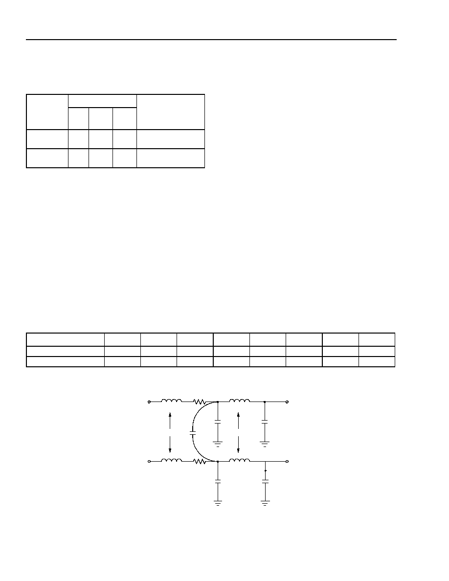
106
106
Agere Systems Inc.
Data Sheet
August 2001
Eight-Channel x 850 Mbits/s Backplane Transceiver
ORCA ORT8850 FPSC
Package Thermal Characteristics
Table 35. ORCA ORT8850 Plastic Package Thermal
Guidelines
* The 680-Pin PBGAM package includes 2 oz copper plates.
Package Coplanarity
The coplanarity limits of the Agere packages are as fol-
lows:
s
PBGAM: 8.0 mils
s
PBGA: 8.0 mils
Package Parasitics
The electrical performance of an IC package, such as
signal quality and noise sensitivity, is directly affected
by the package parasitics. Table 36 lists eight parasit-
ics associated with the ORCA packages. These para-
sitics represent the contributions of all components of a
package, which include the bond wires, all internal
package routing, and the external leads.
Four inductances in nH are listed: L
SW
and L
SL,
the
self-inductance of the lead; and L
MW
and L
ML
, the
mutual inductance to the nearest neighbor lead. These
parameters are important in determining ground
bounce noise and inductive crosstalk noise. Three
capacitances in pF are listed: C
M
, the mutual capaci-
tance of the lead to the nearest neighbor lead; and C
1
and C
2
, the total capacitance of the lead to all other
leads (all other leads are assumed to be grounded).
These parameters are important in determining capaci-
tive crosstalk and the capacitive loading effect of the
lead. Resistance values are in m
.
The parasitic values in
Table 36 are for the circuit
model of bond wire and package lead parasitics. If the
mutual capacitance value is not used in the designer's
model, then the value listed as mutual capacitance
should be added to each of the C
1
and C
2
capacitors.
Package
JA
(∞C/W)
T = 70 ∞C Max,
T
J
= 125 ∞C Max,
0 fpm (W)
0
fpm
200
fpm
500
fpm
352-Pin
PBGA
19.0
16.0
15.0
2.90
680-Pin
PBGAM*
13.4
11.5
10.5
4.10
Table 36. ORCA ORT8850 Package Parasitics
5-3862(C)r2
Figure 25. Package Parasitics
Package Type
L
SW
L
MW
R
W
C
1
C
2
C
M
L
SL
L
ML
352-Pin PBGA
5.0
2.0
220
1.5
1.5
1.5
7.0--12.0 3.0--6.0
680-Pin PBGAM
3.8
1.3
250
1.0
1.0
0.3
2.8--5.0
0.5--1.0
PAD N
BOARD PAD
C
M
C
1
L
SW
R
W
L
SL
L
MW
C
2
C
1
L
ML
C
2
PAD N + 1
L
SW
R
W
L
SL
CIRCUIT

Agere Systems Inc.
107
Data Sheet
August 2001
Eight-Channel x 850 Mbits/s Backplane Transceiver
ORCA ORT8850 FPSC
Package Outline Diagrams
Terms and Definitions
Basic Size (BSC): The basic size of a dimension is the size from which the limits for that dimension are derived by
the application of the allowance and the tolerance.
Design Size: The design size of a dimension is the actual size of the design, including an allowance for fit and tol-
erance.
Typical (TYP): When specified after a dimension, this indicates the repeated design size if a tolerance is specified
or repeated basic size if a tolerance is not specified.
Reference (REF): The reference dimension is an untoleranced dimension used for informational purposes only. It
is a repeated dimension or one that can be derived from other values in the drawing.
Minimum (MIN) or Maximum (MAX): Indicates the minimum or maximum allowable size of a dimension.
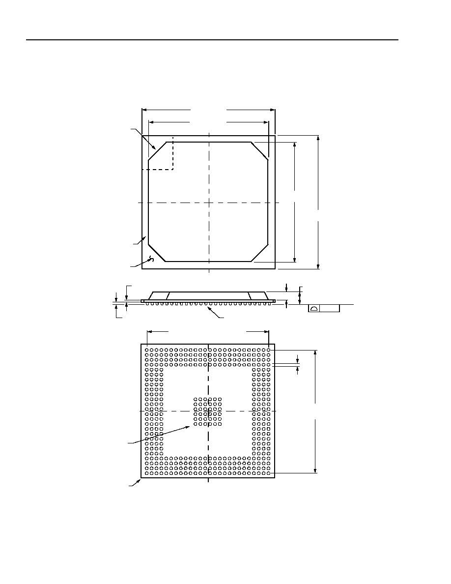
108
Agere Systems Inc.
Data Sheet
August 2001
Eight-Channel x 850 Mbits/s Backplane Transceiver
ORCA ORT8850 FPSC
Package Outline Drawings
352-Pin PBGA
Dimensions are in millimeters.
5-4407(F)
Note: Although the 36 thermal enhancement balls are stated as an option, they are standard on the 352 FPGA package.
0.56
±
0.06
1.17
±
0.05
2.33
±
0.21
SEATING PLANE
SOLDER BALL
0.60
±
0.10
0.20
PWB
MOLD
COMPOUND
35.00
+0.70
≠0.00
30.00
A1 BALL
IDENTIFIER ZONE
AF
AE
AD
AC
AB
AA
Y
W
V
U
T
R
G
25 SPACES @ 1.27 = 31.75
P
N
M
L
K
J
H
1 2 3 4 5 6 7 8 9 10
12
14 16
18
22
24
26
20
11 13
15
17
21
19
23
25
F
E
D
C
B
A
CENTER ARRAY
25 SPACES
A1 BALL
0.75
±
0.15
35.00
±
0.20
30.00
+0.70
≠0.00
±
0.20
@ 1.27 = 31.75
FOR THERMAL
ENHANCEMENT
(OPTIONAL)
CORNER
(SEE NOTE BELOW)
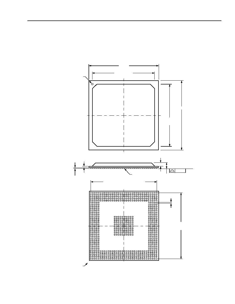
Agere Systems Inc.
109
Data Sheet
August 2001
Eight-Channel x 850 Mbits/s Backplane Transceiver
ORCA ORT8850 FPSC
Package Outline Diagrams
(continued)
680-Pin PBGAM
Dimensions are in millimeters.
5-4406(F)
SEATING PLANE
SOLDER BALL
0.50 ± 0.10
0.20
35.00
T
D
H
AL
F
K
B
P
M
L
J
AH
R
C
E
Y
N
U
AN
G
AD
V
AM
AJ
AG
AE
AC
AA
W
AP
AK
AF
AB
A
19
30
26
28
24
32
22
20
18
4
6
8
10
12
14
16
2
34
5
23
25
7
31
29
15
21
3
27
11
17
9
13
1
33
33 SPACES @ 1.00 = 33.00
33 SPACES
A1 BALL
0.64 ± 0.15
A1 BALL
@ 1.00 = 33.00
CORNER
30.00
1.170
+ 0.70
≠ 0.00
35.00
30.00
+ 0.70
≠ 0.00
IDENTIFIER ZONE
2.51 MAX
0.61 ± 0.08
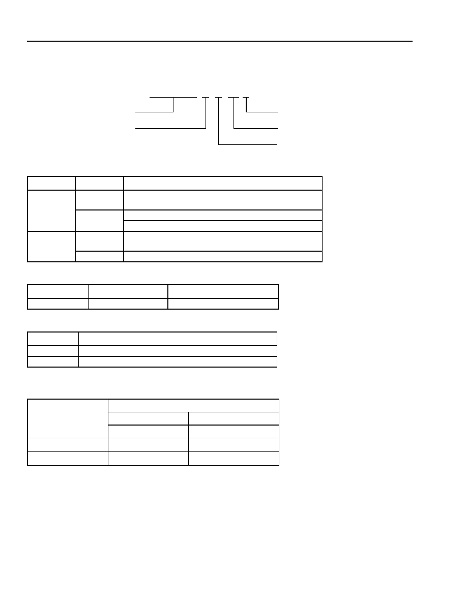
110
Agere Systems Inc.
Data Sheet
August 2001
Eight-Channel x 850 Mbits/s Backplane Transceiver
ORCA ORT8850 FPSC
Hardware Ordering Information
5-6435(F)p
Table 37. Device Type Options
Table 38. Temperature Options
Table 39. Package Type Options
Table 40. ORCA FPSC Package Matrix
(Speed Grades)
Device
Parameter
Value
ORT8850L
Voltage
1.5 V core.
3.3 V/2.5 V I/O.
Package
680-pin PBGAM.
352-pin PBGA. (Four channels with redundancy only.)
ORT8850H
Voltage
1.5 V core.
3.3 V/2.5 V I/O.
Package
680-pin PBGAM.
Symbol
Description
Temperature
(Blank)
Industrial
≠40 ∞C to +85 ∞C
Symbol
Description
BM
Plastic Ball Grid Array, Multilayer
BA
Plastic Ball Grid Array
Device
Package
680-Pin PBGAM
352-Pin PBGA
BM680
BA352
ORT8850L
≠1, ≠2, ≠3
≠1, ≠2, ≠3
ORT8850H
≠1, ≠2, ≠3
--
DEVICE TYPE
PACKAGE TYPE
ORT8850(L)(H)
BM
NUMBER OF PINS
TEMPERATURE RANGE
680
-2
SPEED GRADE

Agere Systems Inc.
111
Data Sheet
August 2001
Eight-Channel x 850 Mbits/s Backplane Transceiver
ORCA ORT8850 FPSC
Software Ordering Information
Implementing a design in an ORT8850H/L requires the ORCA Foundry Development System and an ORT8850
FPSC Desgin Kit. For ordering information, please visit:
http://www.agere.com/netcom/ipkits/ort8850/

Agere Systems Inc. reserves the right to make changes to the product(s) or information contained herein without notice. No liability is assumed as a result of their use or application. ORCA is
a registered trademark of Agere Systems Inc. Foundry is a trademark of Xilinx.
Copyright © 2001 Agere Systems Inc.
All Rights Reserved
August 2001
DS01-198NCIP (Replaces DS01-094NCIP)
For additional information, contact your Agere Systems Account Manager or the following:
INTERNET:
http://www.agere.com or for FPGAs/FPSCs: http://www.agere.com/orca
E-MAIL:
docmaster@agere.com
N. AMERICA:
Agere Systems Inc., 555 Union Boulevard, Room 30L-15P-BA, Allentown, PA 18109-3286
1-800-372-2447, FAX 610-712-4106 (In CANADA: 1-800-553-2448, FAX 610-712-4106)
ASIA:
Agere Systems Hong Kong Ltd., Suites 3201 & 3210-12, 32/F, Tower 2, The Gateway, Harbour City, Kowloon
Tel. (852) 3129-2000, FAX (852) 3129-2020
CHINA: (86) 21-5047-1212 (Shanghai), (86) 10-6522-5566 (Beijing), (86) 755-695-7224 (Shenzhen)
JAPAN: (81) 3-5421-1600 (Tokyo), KOREA: (82) 2-767-1850 (Seoul), SINGAPORE: (65) 778-8833, TAIWAN: (886) 2-2725-5858 (Taipei)
EUROPE:
Tel. (44) 7000 624624, FAX (44) 1344 488 045
Data Sheet
August 2001
Eight-Channel x 850 Mbits/s Backplane Transceiver
ORCA ORT8850 FPSC
Motorola is a registered trademark and RapidIO is a trademark of Motorola, Inc.
EIA is a registered trademark of Electronic Industries Association.
IEEE is a registered trademark of The Institute of Electrical and Electronics Engineers, Inc.
PAL is a trademark of Advanced Micro Devices, Inc.
PowerPC is a registered trademark of International Business Machines, Corporation.
AMBA is a trademark and ARM is a registered trademark of Advanced RISC Machines Limited.
Synopsys Smart Model is a registed trademark of Synopsys, Inc.