PVP 9390A
Picture-in-Picture IC
Version A11
Edition May 3, 2004
6251-633-1AI
ADVANCE INFORMATION
MICRONAS
MICRONAS

2
May 3, 2004; 6251-633-1AI
Micronas
Contents
Page
Section
Title
PVP 9390A
ADVANCE INFORMATION
4
1.
General Description
4
1.1.
Features
6
1.2.
Block Diagram
7
2.
Functional Description
7
2.1.
Analog Front-end
7
2.1.1.
Input Selection
7
2.1.2.
AD-Conversion
7
2.1.3.
Automatic Gain Control
8
2.1.4.
Signal Magnitudes
9
2.2.
Inset Synchronization
9
2.3.
Chroma Decoding And Standard Identification
10
2.4.
Comb Filtering
10
2.5.
Luminance Processing
11
2.6.
Decimation
11
2.6.1.
Single PIP Mode
11
2.6.2.
Continuos Zoom
13
2.6.3.
Horizontal And Vertical Fine Positioning
13
2.6.4.
Multi Display Mode
14
2.6.5.
Split Screen
14
2.6.6.
Multi-PIP Mode
15
2.7.
Display Control
17
2.7.1.
100 Hz Frame Mode
18
2.7.2.
Mixed Standard Applications and (S)VGA Support
19
2.7.3.
Display Standard
19
2.7.4.
Picture Positioning
20
2.7.5.
Wipe In/Wipe Out
21
2.8.
Output Signal Processing
21
2.8.1.
Luminance Peaking
21
2.8.2.
RGB Matrix
22
2.8.3.
Frame Generation And Colored Background
22
2.8.4.
16:9 Inset Picture Support
23
2.8.5.
Parent Clock Generation
23
2.8.6.
Select Signal
23
2.8.7.
Automatic Brightness Reduction
23
2.9.
On Screen Display (OSD)
23
2.9.1.
Display Format
24
2.9.2.
Character Programming
24
2.9.3.
Character and Character Background Color
24
2.10.
DA-Conversion And RGB/YUV Switch
25
2.10.1.
Pedestal Level Adjustment
25
2.10.2.
Contrast, Brightness and Peak Level Adjustment
27
2.11.
Data Slicer
27
2.11.1.
Closed Caption
27
2.11.2.
Wide-screen Signalling (WSS)
27
2.11.3.
Indication of New Data
28
2.11.4.
Violence Protection

Micronas
May 3, 2004; 6251-633-1AI
3
Contents, continued
Page
Section
Title
ADVANCE INFORMATION
PVP 9390A
29
2.12.
Diagrams
31
2.13.
OSD Character Set
32
3.
I
2
C Bus
32
3.1.
I
2
C Bus Address
32
3.2.
I
2
C Bus Format
33
3.3.
I
2
C Bus Command TableI
35
3.4.
I
2
C Bus Command Description
90
4.
Specifications
90
4.1.
Outline Dimensions
91
4.2.
Pin Connections and Short Descriptions
93
4.3.
Pin Configurations
94
4.4.
Electrical Characteristics
94
4.4.1.
Absolute Maximum Ratings
95
4.4.2.
Recommended Operating Conditions
96
4.4.3.
Recommended Crystal Characteristics
97
5.
Application
97
5.1.
Application Circuit
98
6.
Data Sheet History

PVP 9390A
ADVANCE INFORMATION
4
May 3, 2004; 6251-633-1AI
Micronas
PVP 9390A
Picture-in-Picture IC
1. General Description
The PVP 9390A is a Picture-in-Picture (PIP) processor
that combines high-quality digital PIP signal process-
ing, digital multistandard color decoding and A/D-D/A-
conversion on a single chip. The device is equipped
with CVBS, Y/C, and YUV input interfaces to display
standard and high-quality video signals e.g. from a
DVD source. The PVP 9390A replaces the Micronas
PIPIV Picture-in-Picture processor and provides
future-proof characteristics.
The integrated digital color decoder is able to decode
all analog TV standards (PAL, NTSC, and SECAM)
and detects the standard automatically. Therefore, the
IC is suited for world-wide use.
A picture reduction from 1/4 to 1/81 of original size,
selectable in fine steps, is possible. The transfer func-
tions of the decimation filters are optimally matched to
the selected picture size reduction and can further-
more be adjusted to the viewer's requirements by a
selectable peaking. A maximum of 324 luminance and
2x81 chrominance pixels per line are stored in the
memory. The PIP supports split-screen applications as
well as multi-PIP display.
1.1. Features
� Single-chip solution
� A/D-conversion for CVBS or Y/C or YUV, multi-
standard color decoding, PLL for synchronization
of inset channel, decimation filtering, embedded
memory, RGB-matrix, D/A-conversion, RGB/YUV
switch, data-slicer and clock generation inte-
grated on chip
� Analog inputs
� 4x CVBS, 2x Y/C, 2x YUV (some inputs shared)
� Clamping of each input
� All ADCs with 8-bit amplitude resolution
� Automatic Gain Control (AGC) for Y and CVBS
� Inset synchronization
� Multiple time constants for reliable synchroniza-
tion
� Automatic recognition of 625 lines/525 lines stan-
dard
� Color decoder
� PAL-B/G, PAL-M, PAL-N(Argentina), PAL60,
NTSC-M, NTSC4.4, and SECAM
� Adjustable color saturation
� Hue control for NTSC
� Automatic chroma control (
-
24 dB ... +6 dB)
� Automatic recognition of chroma standards:
different search strategies selectable
� Single crystal for all standards
� IF-characteristic compensation filter
� Decimation
� PIP sizes between 1/81 and 1/4 adjustable in
steps of 2 lines and 4 pixel
� Resolution up to 324 luminance and 2x81 chromi-
nance pixels per inset line
� Horizontal and vertical filtering dependent on pic-
ture size
� Automatic zoom in/out possible in three speeds
� Display features
� 7 bits per pixel stored in memory
� Field and joint-line free frame mode display (even
at 100/120 Hz AABB with picture sizes
1/9)
� Two "split-screen" modes with horizontal decima-
tion of 2 and vertical of 1.5 or 1.0 (1.0 with single-
scan 50/60 Hz display only)
� POP display
� Up to 12 pictures of 1/36th size (11 still and 1
moving)
� Up to 6 pictures of 1/16th size (5 still and 1 mov-
ing)
� Up to 3 pictures of 1/9th size (2 still and 1 mov-
ing)
� Display on VGA and SVGA screen (f
H
limited to
40 kHz)
� 8 different read frequencies for 16:9 compatibility
� Line-doubling mode for progressive scan applica-
tions
� Freeze picture
� Coarse positioning at 4 corners of the parent pic-
ture
� Fine positioning at steps of 4 pixels and 2 lines
� Wipe in/out programmable with 3 time periods
� Output signal processing
� 7-bit DAC
� RGB or YUV switch: Insertion of an external
source without PIP processing
� Digital interpolation for anti-imaging
� Adjustable transient improvement for luma (peak-
ing)
� Contrast, brightness, and pedestal level adjust-
able
� Analog outputs: Y, +(B
-
Y), +(R
-
Y), or
Y,
-
(B
-
Y),
-
(R
-
Y) or RGB
� Three RGB matrices available: NTSC(Japan),
NTSC(USA), or EBU
� 64 different background colors and 4096 different
frame colors
� Plain or 3D-frame with variable width and height

ADVANCE INFORMATION
PVP 9390A
Micronas
May 3, 2004; 6251-633-1AI
5
� Data slicing
� Slicing of Closed Caption (CC) or wide-screen-
signaling (WSS) data
� Violence blocking capability (V-chip)
� Several filter for XDS data extraction
� On-screen display
� 64 characters programmable
� 5 characters displayed in every PIP picture or 3
rows of 20 characters each
� 4 different character luminance values or frame
color
� 4 background luminance values or (semi-) trans-
parent mode
� I
2
C Bus control (400 kHz)
� High-stability clock generation
� PMQFP44-1 (lead- and halogen-free) package
(SMD)
� SDA 9488x and SDA 9588x as well as SDA 9489x
and SDA 9589x software backward compatibility
� 3.3 V and 1.8 V supply voltage
PVP 9390A
ADVANCE INFORMATION
6
May 3, 2004; 6251-633-1AI
Micronas
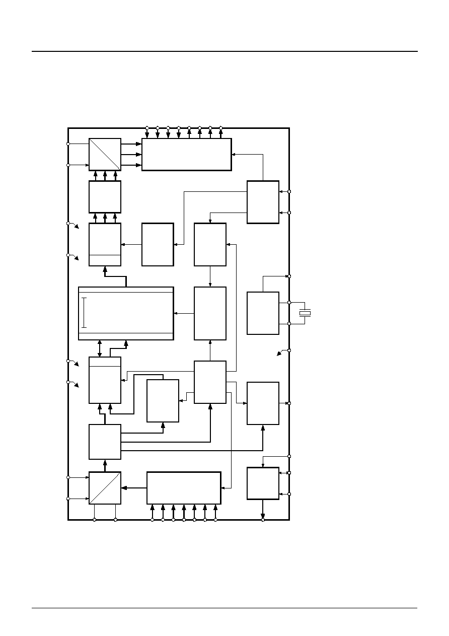
1.2. Block Diagram
Fig. 1�1: Block Diagram
RGB
Matr
ix
P
eaking
Ov
er-
sampling
Inser
tion
RAM
768kbit
OSD &
F
r
ame
Gener
ation
Displa
y
Controller
P
arent
Sync
Processing
Cloc
k
Synthesiz
er
Memor
y
Controller
Sk
e
wcomp
.
H/V Scaler
Decimation
Color
Decoder
P
AL/SECAM/
NTSC
Y/C &
Sync
Separ
ation
Inset
Sync
Processing
Input
Select
Clamp
Gain
DEMUX
Data Slicer
Acquisition
I
2
C
Controller
MUX
3x ADC
8bit
T
r
iple
DA
C
3x7bit
IN1
IN3
FSW
OUT1
OUT2
OUT3
SEL
F
ast
RGB/YUV
Switch
IN2
VDD33D
A
C
VSS33D
A
C
VDD18
VSS18
CVBS1
CVBS2
CVBS3
VSS33ADC
VDD18ADC
XIN
XQ
I2C1
SCL
SD
A
HSP
VSP
XT
AL
20.25 MHz
INTR
CVBS4
Y
U
V
CLK
OUT
GP0..2
I2C2
VDD33P
A
D
VSS33P
AD
VSS18ADC
VDD33ADC
RESET
PVP 9390A
ADVANCE INFORMATION
PVP 9390A
Micronas
May 3, 2004; 6251-633-1AI
7
2. Functional Description
2.1. Analog Front-end
2.1.1. Input Selection
An analog inset CVBS signal can be applied to the
inputs CVBS1-3 of PVP 9390A. Each of these sources
is selectable via I
2
C bus (CVBSEL). Additionally
CVBS4 can be enabled with INSEL. CVBS1/CVBS2
and CVBS2/CVBS3 can be used as separate Y/C
inputs. YUV sources can be connected to CVBS1,
CVBS2 and CVBS3 or to Y, U, V. The YUV source is
enabled by YUVSEL or INSEL. The PVP 9390A can
operate in applications with both YUV and CVBS sig-
nals without an external switch. See Fig. 2�1.
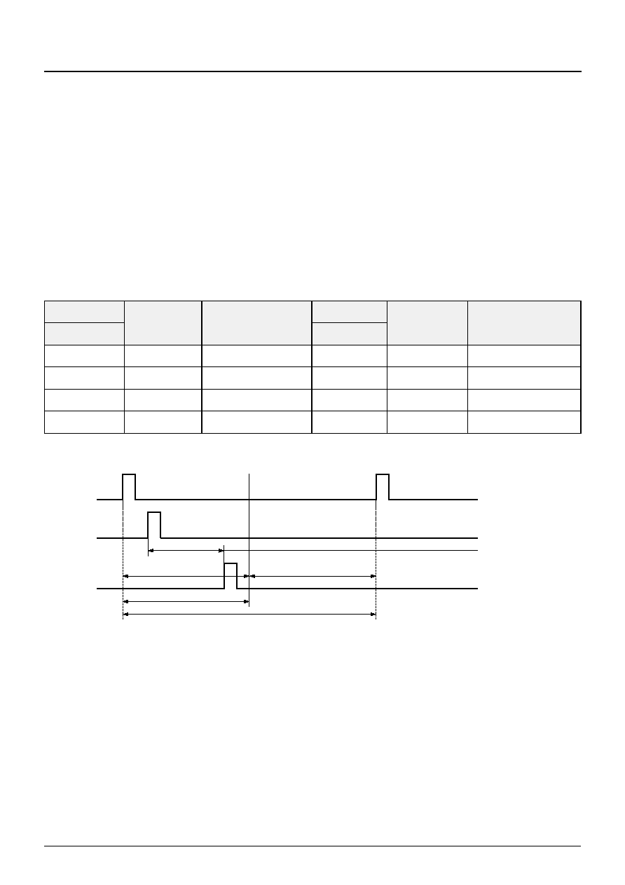
2.1.2. AD-Conversion
All signal are clamped and AD-converted with an
amplitude resolution of 8 bit. CVBS and Y signals are
clamped to the sync bottom or backporch, selectable
by CLMSTGY. U/V and C signals are always clamped
to their mid-level during blanking.
The clamping pulse can be shifted in position (CLMP-
IST) and length (CLMPID) to adjust to the specific
application. The ADCs are driven by a 20.25 MHz free
running crystal clock which is not related to the incom-
ing CVBS signal.
To avoid aliasing by sub-sampling the CVBS signal
and the Y/C signals should be band-limited to 10 MHz.
In the same manner the U/V signal frequency spec-
trum should not exceed 5 MHz. Analog anti-alias filter
can be enabled for each channel. The digital filtering
suppresses all frequencies above the usable spec-
trum.
2.1.3. Automatic Gain Control
To accommodate to different CVBS input voltages an
automatic gain control has been implemented. The
chip works correctly for input voltages in the range
from 0.5 to 1.5 V
pp
. For best signal-to-noise ratio, the
maximum CVBS amplitude is recommended if avail-
able. The AGC behavior can be chosen out of four
possibilities (AGCMDE).
The sync height serves as reference for the gain con-
trol in the typical application. When using overflow
detection only, the gain is set to maximum and is
reduced whenever an overflow occurs. This procedure
will be executed again when a channel change is
detected or the gain control is manually reset by
AGCRES.
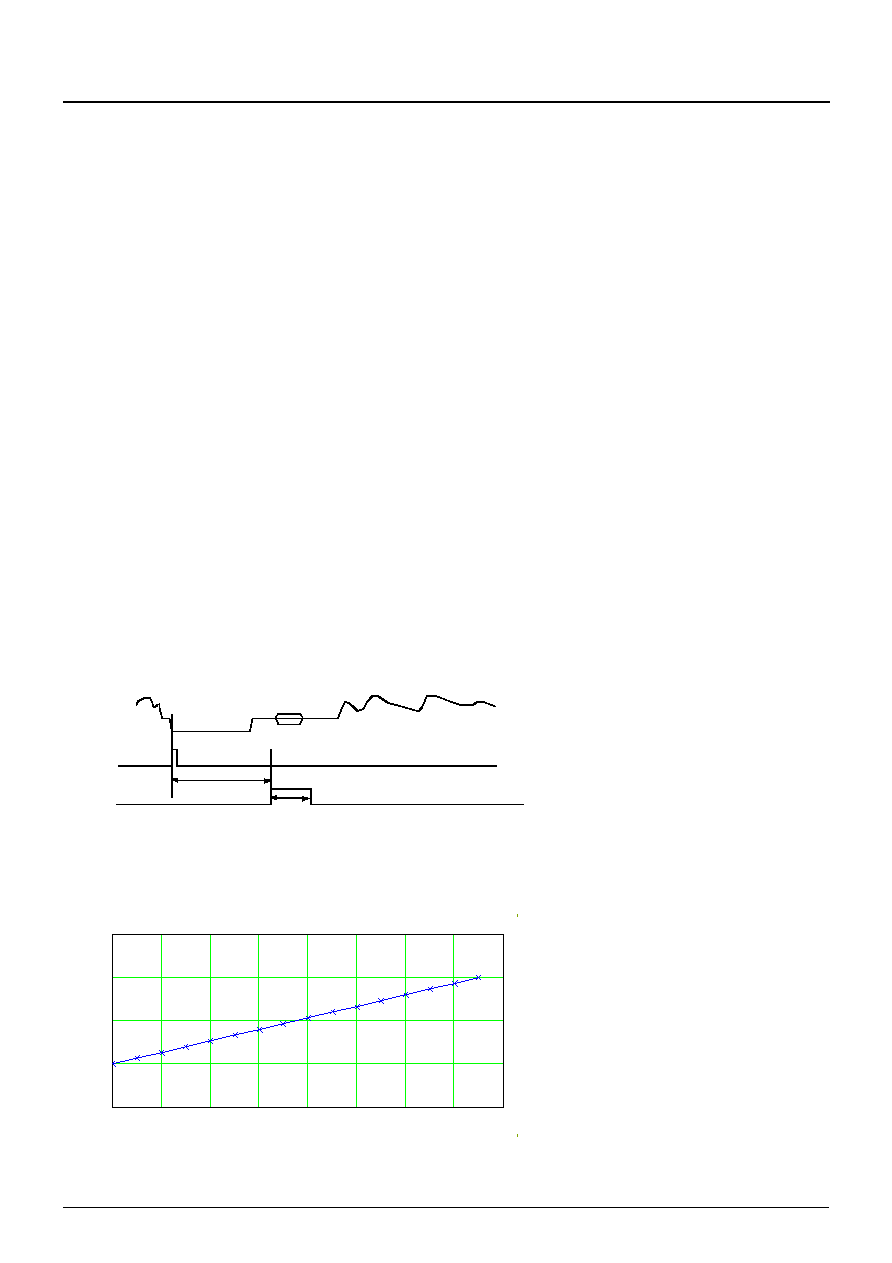
Fig. 2�1: Clamping Timing
Fig. 2�2: AGC Characteristic
I ns et
V id eo
HD
CLAMPI
C LMPID
CLMPIST
0
2
4
6
8
10
12
14
16
0
0.5
1
1.5
2
Automatic Gain Control Characteristic
AGCVAL
I
nput V
o
lta
ge
[
V
]
PVP 9390A
ADVANCE INFORMATION
8
May 3, 2004; 6251-633-1AI
Micronas
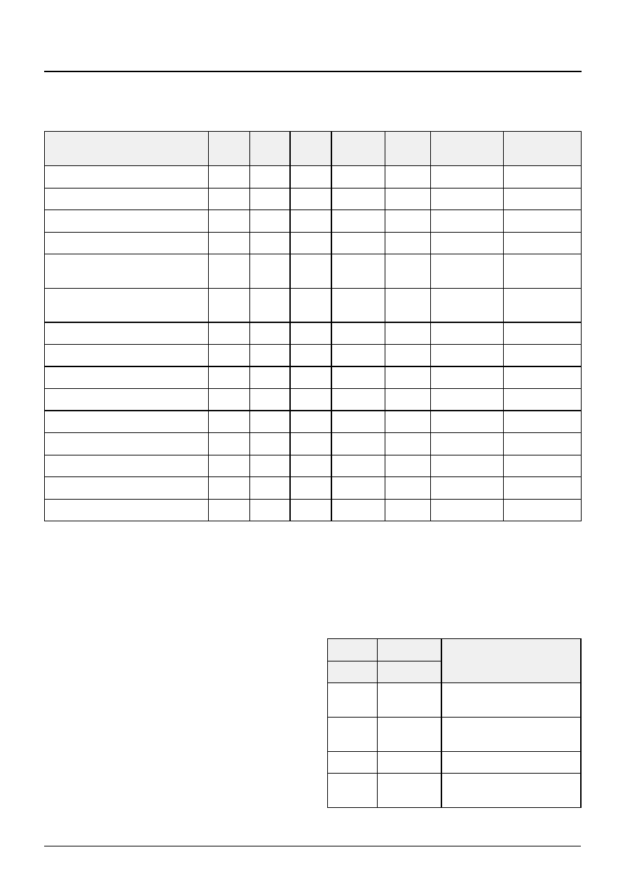
2.1.4. Signal Magnitudes
The nominal CVBS signal with 75 % color has a mag-
nitude of 1 V
pp
. The upper headroom is left to permit
signals with 100 % color resulting in 1.23 V
pp
. The Y-
signal must always contain the sync part. Its levels cor-
respond to the CVBS levels except for the missing
color and burst. After A/D conversion the video part is
clamped to its black value and is amplified to 224 digi-
tal steps. The nominal signal levels ensure correct
brightness and saturation. The YUV signal levels con-
form to the ITU 601 recommendation.
Fig. 2�3: CVBS/Y and Chroma ADC Input Signal Range
Fig. 2�4: UV Input Signal Range
Table 2�1: Input selection
INSEL
CVBSEL
YUVSEL
Input
D1
D0
D7
D6
D4
CVBS1
CVBS2
CVBS3
CVBS4
Y
U
V
0
0
0
0
0
CVBS
0
0
0
1
0
CVBS
0
0
1
0
0
Y
S
C
0
0
1
1
0
CVBS
0
0
x
x
1
Y
S
U (P
B
)
V (P
R
)
0
1
x
x
x
CVBS
1
0
x
x
x
Y
S
C
1
1
x
x
x
Y
S
U (P
B
)
V (P
R
)
lower headroom
SR
Y =
1
V
p
p
CRY
C
= 1.
2 V
p
p
S
R
C
=
0.
89
V
p
p
75
% chr
o
m
a
10
0%
c
h
r
o
m
a
bu
r
s
t
white
black
bu
r
s
t
0
32
128
224
255
0
68
217
255
4
CRY
C
= 1.
2 V
p
p
upper headroom
upper headroom
lower headroom
CRUV
=
0.
8 Vp
p
S
R
UV
=
0.
7
V
p
p
0
16
128
240
255
75% U
212
44
CRUV
=
0.8 V
p
p
S
R
UV
=
0.7
Vpp
0
16
128
240
255
212
44
lower headroom
upper headroom
upper headroom
lower headroom
75% V
ADVANCE INFORMATION
PVP 9390A
Micronas
May 3, 2004; 6251-633-1AI
9
2.2. Inset Synchronization
Horizontal and vertical sync pulses are separated after
elimination of the high frequency components of the
CVBS signal by a low pass filter. Horizontal sync
pulses are generated by a digital phase-locked-loop
(DPLL). Its time constant is adjustable between fast
and slow behavior in four steps (PLLITC) to consider
different input sources (e.g. VCR). Noisy input signals
become more stable when a noise-reduction is
enabled (NSRED). Additionally weak input signals
from a satellite dish ('fishes') become more stable
when SATNR is enabled. Both should be enabled to
have best available performance. A vertical flywheel
mode improves vertical sync separation for weak sig-
nals (VFLYWHL, VFLYWHLMD). Additionally, v-syncs
may be gated by VTHRL50/60 and VTHRH50/60 to
reject invalid v-syncs. Dependent on detected line
standard, the VTHRx50 or VTHRx60 setting is used.
50 Hz or 60 Hz operation for sync separation may be
forced separately or selected to work automatically
(FLNSTRD).When NOSIGB is enabled, a colored
background is shown instead of the picture when PIP
is out of (horizontal) synchronization. The detected line
standard is indicated by SYNCSTAT.
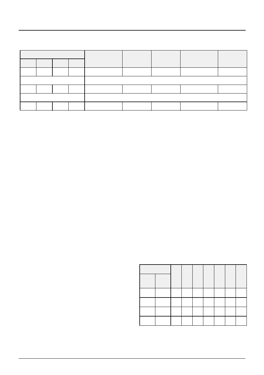
2.3. Chroma Decoding And Standard Identification
The system is able to decode NTSC and PAL signals
with a subcarrier of 3.58 MHz and 4.43 MHz (PAL B/M/
N/60, NTSC M/4.4) as well as SECAM signals with
4.05/4.2 MHz subcarrier. The system may be forced to
a certain standard, or an automatic standard detection
can be used (CSTAND). For automatic standard
detection, some standards which are not likely to be
received can be ignored to improve the detection pro-
cess (CSTDEX).
Depending on the detected line standard (525 or
625 lines) the color standard detection circuit searches
for 60 Hz signals (NTSC-M/PAL-M/PAL 60/NTSC44) or
50 Hz signals (PAL-B/SECAM/PAL-N) respectively.
Within each line standard, the standard is detected by
consequently switching from one to another. This stan-
dard detection process can be set to slow or fast
behavior (LOCKSP). In slow behavior, 25 fields are
used to detect the standard, whereas 15 fields are
used in fast behavior. If unsuccessful within this time
period the system tries to detect another standard. For
SECAM detection, a choice between different recogni-
tion levels is possible (SCMIDL, SECACCL, SECDIV)
and the evaluated burst position is selectable
(BGPOS).
For getting the chrominance information the digitized
video signal is multiplied with the regenerated color
subcarrier once in-phase and once phase-shifted by
90 �. After lowpass filtering digital UV is available for
PAL and NTSC. The subcarrier is regenerated by a
digital PLL. At SECAM operation the PLL runs free and
generates the line-wise alternating subcarriers. A
CORDIC structure demodulates the frequency-modu-
lated UV signals. The following SECAM de-emphasis
filter characteristic is adjustable (DEEMP).
The chroma signal can be filtered before demodulation
by means of a selectable IF-prefilter (IFCOMP).
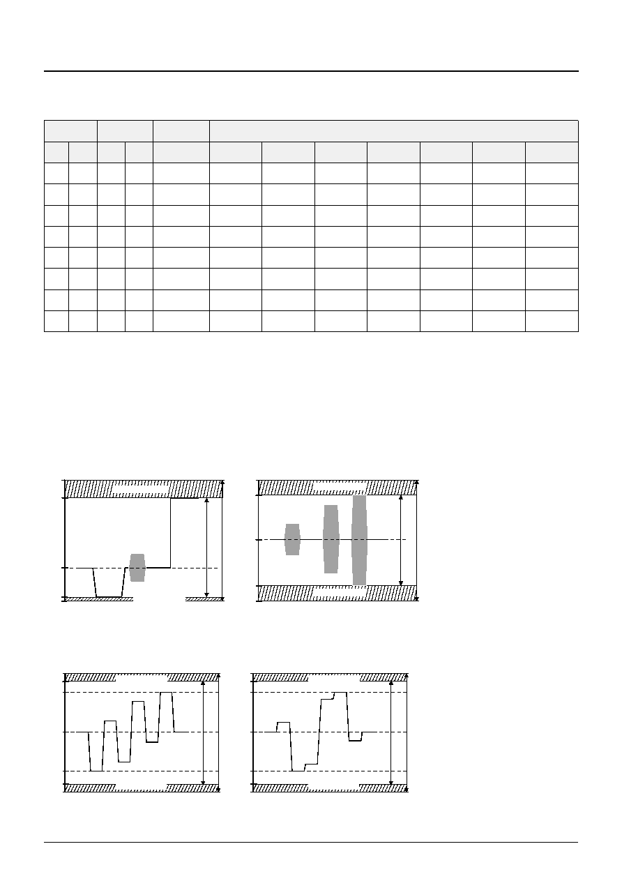
Table 2�2: ADC conversion range and required input signal voltage
AGCVAL
Conversion
Range
CRYC
Signal
Range
SRY
Signal
Range
SRC
Conversion
Range
CRUV
Signal
Range
SRUV
D4
D3
D2
D1
0
0
0
0
0.5 Vpp
0.42 Vpp
...
1
0
0
0
1.2 Vpp
1.0 Vpp
0.89 Vpp
0.8 Vpp
0.7 Vpp
...
1
1
1
1
1.5 Vpp
1.25 Vpp
Table 2�3: Considered color standards for automatic
standard detection
CSTDEX
NTSC-M
PA
L
6
0
PA
L
-
N
PA
L
-
M
PA
L
-
B
SEC
AM
NTSC 44
D4
D3
0
0
0
1
1
0
1
1
PVP 9390A
ADVANCE INFORMATION
10
May 3, 2004; 6251-633-1AI
Micronas
The Hue control (HUE) influences the phase of the
demodulation subcarrier between
-
44.8 � and 43.4 � in
steps of 1.4 �. This is provided for NTSC only and
adjustment is ineffective for PAL and SECAM signals.
The reference for the subcarrier generation is a crystal
stable clock of 20.25000 MHz. In order to avoid color
standard detection problems, the maximum deviation
of this frequency should not exceed 100 ppm. For a
good PLL locking behavior a maximum deviation of
40 ppm is recommended. A small frequency adjust-
ment (
-
150 ... +310 ppm) is possible for using a crystal
with small frequency deviations (SCADJ). For test pur-
poses, CPLL allows to open the loop of the chroma
PLL.
For deviations in the chroma signal up to 30 dB, a sta-
ble output amplitude after chroma decoding is
achieved due to the ACC (Automatic Chroma Control).
If the chroma signal (color burst) is below a selectable
threshold (CKILL), the color will be switched off. Alter-
natively the color-killer can be bypassed and the color
can be switched on or off under all conditions
(COLON). By setting ACCFIX, the automatic chroma
control is disabled and set to a default value.
The bandwidth of the chroma filter is adjustable via
CHRBW. The bandwidth depends on whether the
decoder is in SECAM operation or not. A change in
CHRBW does not result in a chrominance position
shift on the screen.
CKSTAT can be read out and gives information
whether the color is switched on or off. STDET indi-
cates the detected color standard. Additionally PALID
and PALDET signal whether a PAL signal is applied.
2.4. Comb Filtering
Depending on the selected picture size and color stan-
dard, a comb filtering is performed for luminance and
chrominance. A comb filter uses the spectral interleav-
ing of the encoded luminance and chrominance to
separate both without cross artifacts. Thus cross-color
and cross-luminance are suppressed effectively. For
NTSC sources, a comb filtering is performed for all pic-
ture sizes. Due to reduced bandwidth in horizontal and
vertical direction a strong reduction of cross artifacts
can be achieved for PAL signals. The same applies for
the luminance signal of SECAM signals.
2.5. Luminance Processing
The A/D-converted CVBS (or Y) signal is digitally
clamped to back porch. Depending on the transmitted
standard and operational area, an offset between
black- and blanking level can be found in the incoming
signal (`7.5 IRE'). As for some applications a black off-
set is not desired, controlling may be done using
LMOFST. The positive or negative offset is added to
the Y signal before scaling.
The color carrier is removed out of a CVBS signal by
means of a notch filter. It is set to the corresponding
color carrier (3.58 or 4.4 MHz) only if the standard is
detected permanently. This prevents the luminance
sharpness of being changed within the standard
search process. For Y signals the notch is disabled. A
special peaking can be applied to the notch-filter
(NADJ) to make it steeper. For a fine adjustment of
delay compensation between luminance and chromi-
nance, YCDEL allows a luminance shifting in 16 steps
of 50 ns.
Fig. 2�5: Black Level Correction of Luminance Signal
Table 2�4: Color killer adjustment
CKILL
COLON
Color Killed at Clamping
of
D1
D0
0
0
0
30 dB
0
1
0
18 dB
1
1
0
24 dB
1
1
0
Color always off
X
X
1
Color always on
Received Signal
BLACK value
BLANK value
LMOFST='00' (no additional offset)
Processed Signal
BLACK value
BLANK value
LMOFST='10' (reduction of 16 LSB)
BLACK value
BLANK value
BLANK value
BLACK value
LMOFST='00' (no additional offset)
LMOFST='01' (addition of 16 LSB)
M Standard Signals
B/G/H/I/N Standard Signals
ADVANCE INFORMATION
PVP 9390A
Micronas
May 3, 2004; 6251-633-1AI
11
2.6. Decimation
2.6.1. Single PIP Mode
Luminance and chrominance signals are filtered in
horizontal and vertical direction. The coarse horizontal
and vertical picture size (1/2, 1/3, 1/4, 1/6) is indepen-
dently programmable with SIZEHOR and SIZEVER. A
fine adjustment in steps of 4 pixel and 2 lines is possi-
ble by HSHRINK and VSHRINK, which allows correct
aspect ratio for multistandard applications (50/60 Hz
mixed mode, (S)VGA).
For main decimation factors, the stored number of
pixel and lines are listed in the following tables.
2.6.2. Continuos Zoom
The continuos zoom feature changes the picture size
rapidly in an animated manner. It is available in single-
PIP mode for picture sizes smaller or equal 1/4 of the
undecimated picture.
There are three possibilities of using the zoom feature:
� The PIP is zoomed via HSHRINK and VSHRINK
manually. This requires an I�C protocol each time
the picture size should change. CZMEN should be
used to synchronize the update of HSHRNK/
VSHRNK with SIZEHOR/SIZEVER.
� A different way is to make usage of the automatic
zooming. The zoom speed can be controlled by
CZMSP. When switching PIP on or off by using
PIPON, the PIP zooms automatically to the selected
picture size or disappears at size of 1/81.
� A zooming between two picture sizes can be per-
formed by changing the HSHRINK, VSHRINK,
SIZEHOR, SIZEVER values, when CZMEN is
enabled. The new picture size is obtained by zoom-
ing and not taken immediately.
Automatic zooming is only possible in frame mode.
Being in field mode, the picture size remains stable
until frame mode occurs or until the internal counter
reaches the desired picture size. Then, the size
changes immediately. Equal to the wipe process, the
zooming direction depends on the coarse position
(CPOS).
Table 2�5: Number of stored pixel per line dependent
on SIZEHOR
SIZEHOR
Horizontal
Scaling
PIP Pixel per Line
D3
D2
Y
(B-Y)
(R-Y)
0
0
2:1
324
81
81
0
1
3:1
216
54
54
1
0
4:1
160
40
40
1
1
6:1
108
27
27
Table 2�6: Number of stored lines per field
SIZEVER
Vertical
Scaling
PIP Lines
D1
D0
625 Lines
Source
525 Lines
Source
0
0
2:1
132
108
0
1
3:1
88
72
1
0
4:1
66
54
1
1
6:1
44
36
PVP 9390A
ADVANCE INFORMATION
12
May 3, 2004; 6251-633-1AI
Micronas
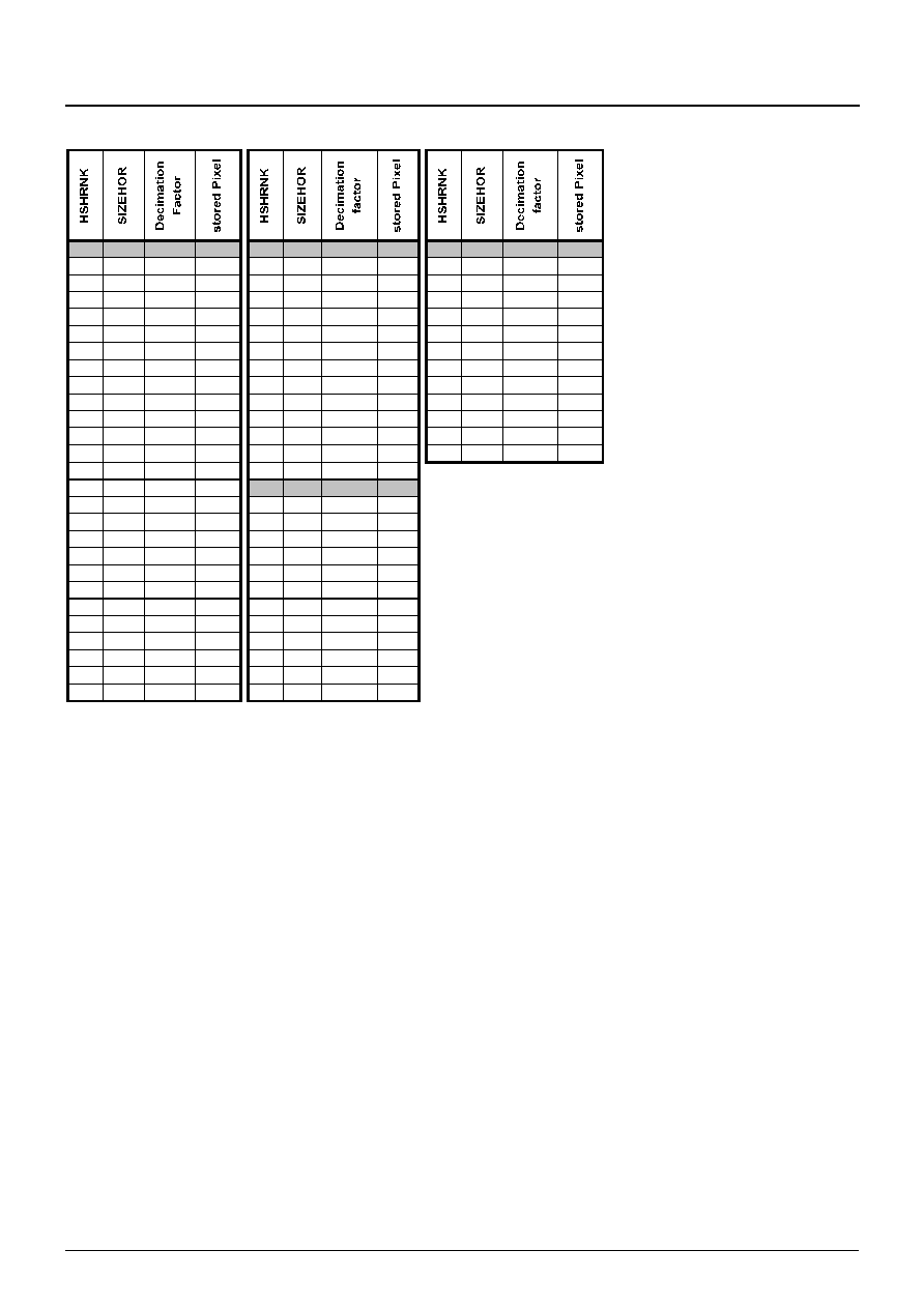
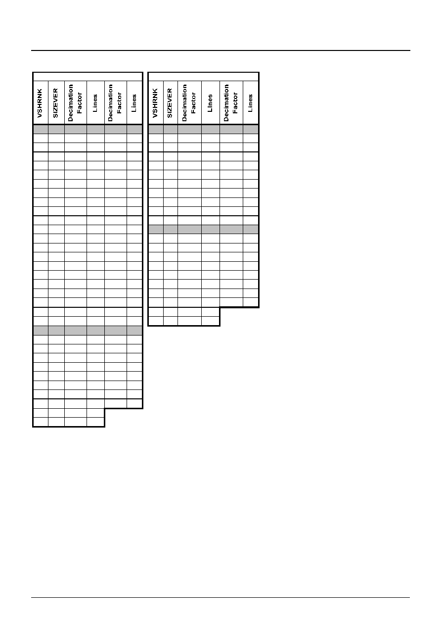
Fig. 2�6: Number of Stored Pixel per Line Dependent on HSHRNK
0
0
2,00
324
0
1
3,00
216
0
3
6,00
108
1
0
2,02
320
1
1
3,04
212
1
3
6,23
104
2
0
2,05
316
2
1
3,11
208
2
3
6,48
100
3
0
2,08
312
3
1
3,17
204
3
3
6,75
96
4
0
2,10
308
4
1
3,23
200
4
3
7,04
92
5
0
2,13
304
5
1
3,29
196
5
3
7,35
88
6
0
2,16
300
6
1
3,37
192
6
3
7,70
84
7
0
2,19
296
7
1
3,44
188
7
3
8,10
80
8
0
2,22
292
8
1
3,51
184
8
3
8,52
76
9
0
2,25
288
9
1
3,60
180
9
3
8,99
72
10
0
2,28
284
10
1
3,67
176
10
3
9,51
68
11
0
2,31
280
11
1
3,76
172
11
3
10,12
64
12
0
2,35
276
12
1
3,84
168
12
3
10,64
60
13
0
2,38
272
13
1
3,94
164
14
0
2,41
268
0
2
4,05
160
15
0
2,45
264
1
2
4,16
156
16
0
2,49
260
2
2
4,27
152
17
0
2,53
256
3
2
4,38
148
18
0
2,57
252
4
2
4,50
144
19
0
2,61
248
5
2
4,63
140
20
0
2,66
244
6
2
4,77
136
21
0
2,70
240
7
2
4,91
132
22
0
2,74
236
8
2
5,06
128
23
0
2,80
232
9
2
5,22
124
24
0
2,84
228
10
2
5,41
120
25
0
2,89
224
11
2
5,59
116
26
0
2,95
220
12
2
5,78
112
ADVANCE INFORMATION
PVP 9390A
Micronas
May 3, 2004; 6251-633-1AI
13
Fig. 2�7: Number of Stored Lines per Field Dependent on VSHRNK
2.6.3. Horizontal And Vertical Fine Positioning
All picture sizes are pre-centered inside the frame. In
addition, if necessary the vertical and horizontal acqui-
sition area can be shifted by VFP for vertical and HFP
for horizontal direction.
2.6.4. Multi Display Mode
The PVP 9390A offers the feature to display a sub-pic-
ture more than once. The picture size and arrange-
ment depends on the display mode (DISPMOD) and
not on SIZEHOR or SIZEVER. Hence variable scaling
is not possible in these modes.
The display modes are shown in the appendix. The
sizes of the partial pictures are listed in Table 2.7. on
page 15
0
0
2 132
2 108
0
2
4
66
4,01
54
1
0
2,03 130
2,03 106
1
2
4,13
64
4,15
52
2
0
2,06 128
2,08 104
2
2
4,25
62
4,31
50
3
0
2,09 126
2,13 102
3
2
4,41
60
4,5
48
4
0
2,13 124
2,16 100
4
2
4,56
58
4,69
46
5
0
2,16 122
2,2
98
5
2
4,72
56
4,9
44
6
0
2,2 120
2,25
96
6
2
4,88
54
5,13
42
7
0
2,23 118
2,3
94
7
2
5,06
52
5,39
40
8
0
2,28 116
2,34
92
8
2
5,28
50
5,7
38
9
0
2,31 114
2,41
90
9
2
5,5
48
10
0
2,36 112
2,45
88
10
2
5,75
46
11
0
2,41 110
2,52
86
0
3
6
44
6
36
12
0
2,44 108
2,58
84
1
3
6,28
42
6,38
34
13
0
2,48 106
2,64
82
2
3
6,61
40
6,75
32
14
0
2,53 104
2,7
80
3
3
6,94
38
7,22
30
15
0
2,59 102
2,77
78
4
3
7,31
36
7,73
28
16
0
2,64 100
2,84
76
5
3
7,78
34
8,3
26
17
0
2,69
98
2,92
74
6
3
8,25
32
9
24
18
0
2,75
96
7
3
8,81
30
9,8
22
19
0
2,81
94
8
3
9,42
28 10,78
20
20
0
2,88
92
9
3 10,17
26
21
0
2,94
90
10
3 11,02
24
0
1
3
88
3
72
1
1
3,07
86
3,09
70
2
1
3,14
84
3,19
68
3
1
3,21
82
3,28
66
4
1
3,3
80
3,38
64
5
1
3,38
78
3,49
62
6
1
3,47
76
3,61
60
7
1
3,56
74
3,73
58
8
1
3,66
72
3,87
56
9
1
3,77
70
10
1
3,89
68
625 lines
525 lines
625 lines
525 lines

PVP 9390A
ADVANCE INFORMATION
14
May 3, 2004; 6251-633-1AI
Micronas
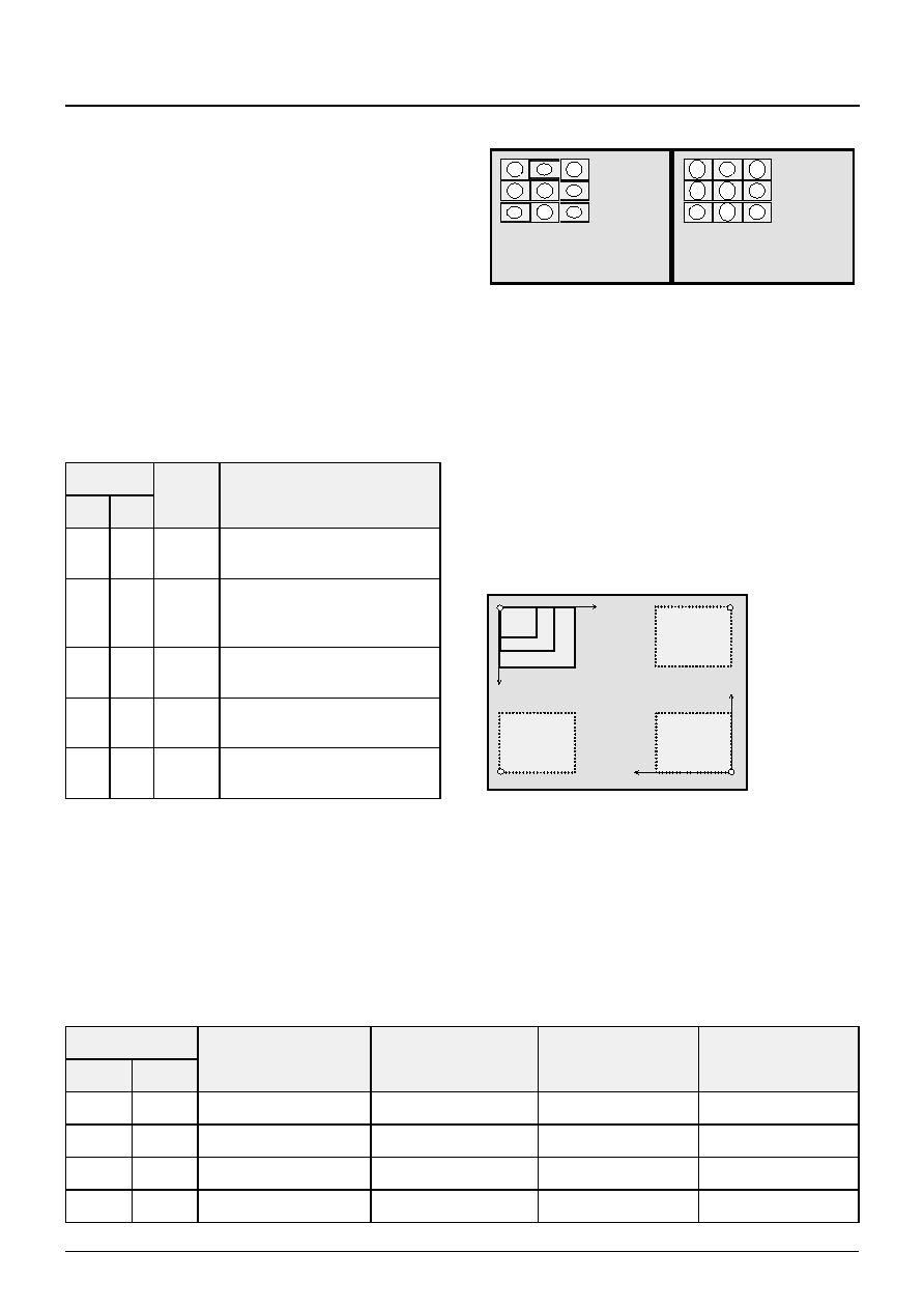
2.6.5. Split Screen
For split screen applications two selectable "double
window" modes in which one half of the picture is gen-
erated by the PVP 9390A can be used. The split
screen mode can be selected by two possible combi-
nations of DISPMOD.
Fig. 2�8: Double Window Mode 1.5 (left picture) and
Mode 1 (right picture)
The D1.5 mode is suited for displaying split screen on
16:9 tubes keeping the aspect ratio. The DW1 format
covers the full height of the screen. The DW1 format is
only suited for 50/60 Hz single-scan applications and
is not suited for 100 Hz or "progressive" displays.
2.6.6. Multi-PIP Mode
There is a great variety of multi-PIP modes available.
Up to 11 different still pictures and one moving picture
can be shown. This is useful to give an overview over
broadcasted programmes (e.g. tuner-scan) or for
supervising purposes. For multi-PIP modes only three
fixed picture sizes are available (1/9, 1/16 or 1/36). The
picture size and arrangement depends on the display
mode (DISPMOD) and not on SIZEHOR or SIZEVER.
Variable scaling is thus not possible in these modes.
Because of limited memory capacity, the number of
frozen multi-pictures is limited dependent on picture
size to the number shown in the table below:
The partial picture that is written is addressed via
WRPOS. With INFRM, a frame for separation of every
PIP can be selected. This is adjustable to single or
dual PIP mode (INFRMOD). The current updated pic-
ture can be highlighted with PIPHLT. To avoid garbage
pictures after switching from one mode to another the
selected picture can be blanked with PIPBLK.
MPIPBG defines wether the picture will be blanked
with black or with the adjusted background color.
For compatibility reasons to other devices, the DISP-
MOD register is split into two segments. If a display
mode is chosen that is not implemented, the PIP inser-
tion is switched off automatically (PIPON = `0'). The
sizes of the partial pictures correspond to the sizes of
the inset pictures of the single PIP modes.
Table 2�7: Multi-display modes
Display
Mode
DISPMOD
Size
Picture Configuration
Pixel
Lines
D6
D5
625
525
1
0
0
SIZEHOR/SIZEVER
HSRHNK/VSHRNK
Single PIP mode
324
60
132
24
108
20
2
0
1
3 X1/9
One upon another (same content)
216
264
216
3
1
0
4 X 1/16
One upon another (same content)
156
264
216
Table 2�8: Maximum number of pictures in multi-PIP
mode
Picture
Sizes
Maximum Number of Pictures
(Including One Live Picture)
1/9
3
1/16
6
1/36
12

ADVANCE INFORMATION
PVP 9390A
Micronas
May 3, 2004; 6251-633-1AI
15
2.7. Display Control
The on-chip memory capacity is 768 kbits. Provided
that the same standard (50 or 60 Hz)
video sources
are applied to inset and parent channel, joint-line free
frame mode display is possible. This means that every
incoming field is processed and displayed by the
PVP 9390A processors. The result is a high vertical
and time resolution. For this purpose the standard is
analyzed internally and the frame mode display is
blocked automatically, if the described restrictions are
not fulfilled. Then, only every second incoming field is
shown (field mode). Field mode normally shows joint-
lines. This is caused by an update of the memory dur-
ing read out. The result is that one part of the picture
contains new picture information and the other part
contains one earlier written field. The switching from or
to frame mode is free of artifacts.
Activation of frame-mode display is blocked automati-
cally when at least one of the following conditions is
not fulfilled:
� Inset and parent channel have the same field repeti-
tion frequency. This means that frame mode is pos-
sible only for 50 Hz inset and parent sources or
60 Hz inset and parent sources.
� Interlace signal is detected for inset and parent
channel. Therefore, for progressive scan or (S)VGA
display, only field mode is possible. For some VCRs
in trick mode, often no interlace is detected.
Table 2�9: Display Modes
Display
Mode
DISPMOD
Size
Picture Configuration
Pixel
Lines
D6
D5
D4
D3
D2
625
525
4
0
0
0
0
1
2 x 1/9,
One upon another
216
176
144
5
0
0
0
1
0
2 x 1/9,
Side by side
432
88
72
6
0
0
0
1
1
3 x 1/9,
Side by side
648
88
72
7
0
0
1
0
0
3 x 1/9
Pne upon another
216
264
216
8
0
0
1
0
1
4 x 1/16
Side by side
624
66
54
9
0
0
1
1
0
6 x 1/16
Inverted U shaped
624
132
108
10
0
0
1
1
1
6 x 1/16
U shaped
624
132
108
11
0
1
0
0
0
4 x 1/16
2 rows of 2 pictures
312
132
108
12
0
1
0
0
1
4 x 1/16
One upon another
156
264
216
13
0
1
0
1
0
12 x 1/36
6 rows of 2 pictures
216
264
216
14
0
1
0
1
1
12 x 1/36
2 rows of 6 pictures
648
88
72
15
0
1
1
0
0
9 x 1/36
3 rows of 3 pictures
324
132
108
16
0
1
1
0
1
12 x 1/36
3 rows of 4 pictures
432
132
108
17
0
1
1
1
0
11 x 1/36
Angular of 11 pictures
648
264
216
18
0
1
1
1
1
9 x 1/36
Angular of 9 pictures
540
220
180
19
1
0
0
0
0
1 x 1/3
Double Window (V=1.5)
324
176
144
20
1
0
0
0
1
1 x 1/2
Double Window (V=1)
1)
324
264
216
21
1
0
0
1
0
OSD only
Others
Reserved
1)
Single-scan display only
PVP 9390A
ADVANCE INFORMATION
16
May 3, 2004; 6251-633-1AI
Micronas
� The number of lines is within a predefined range for
inset (FMACTI) or parent (FMACTP) channel
(assuming standard signals according to ITU)
The system may be forced to field mode by means of
FIESEL. Either first or second field is selectable. "One
of both" takes every second field independent of the
field number. This is meant for sources generating only
one field (e.g. video-games).
For progressive scan conversion systems and HDTV/
(S)VGA displays a line doubling mode is available
(PROGEN). Every line of the inset picture is read
twice.
Memory writing is stopped by FREEZE bit. The field
stored in the memory is then continuously read. As the
picture decimation takes place before storing, the pic-
ture size of a frozen picture can not be changed.
Synchronization of memory reading with the parent
channel is achieved by processing the parent horizon-
tal and vertical synchronization signals connected to
the pin HSP for horizontal synchronization and pin
VSP for vertical synchronization. HSPINV or VSPINV
respectively allow an inversion of the expected signal
polarity.
Fig. 2�9: Field Detection and Phase Adjustment of Vertical Pulse (VSP)
Depending on the phase between inset and parent sig-
nals a correction of the display raster for the read out
data is performed. As the external VSP and HSP sig-
nals may come from different devices with different
delay paths, the phase between V-sync and H-sync is
adjustable (VSPDEL). An incorrect setting of VSPDEL
may result in wrong or unreliable field detection of par-
ent channel.
Normally a noise reduction of the incoming parent ver-
tical pulse is performed. With this function missing ver-
tical pulses are compensated. The circuit works for 50/
60 Hz applications as well as progressive and 100/
120 Hz application. (S)VGA signals are supposed to
be very stable and therefore not supported by the
noise suppression. By means of VSPNSRQ, vertical
noise suppression is switched off.
A great variety of combinations of inset and parent fre-
quencies are possible. Table 2�11 on page 17 shows
some constellations.
Table 2�10: Required number of lines for frame mode display
FMACTP
Parent
Standard
Number of Lines
per Field
FMACTI
Inset
Standard
Number of Lines
per Field
D3
D6
0
50 Hz
310...315
0
50 Hz
310...315
1
50 Hz
290...325
1
50 Hz
290...325
0
60 Hz
260...265
0
60 Hz
260...265
1
60 Hz
250...275
1
60 Hz
250...275
VSPDEL
VSPDEL
max
=151 (75)
�s
values in brackets () apply for 100Hz systems
field 0 window
field 1 window
tH = 64 (32)
�s
tH/2 = 32 (16)
�s
HSP
VSP
VSPD
(internal)

ADVANCE INFORMATION
PVP 9390A
Micronas
May 3, 2004; 6251-633-1AI
17
2.7.1. 100 Hz Frame Mode
If the picture size is smaller or equal than 1/9 PIP a
true frame mode display for 100 Hz parent standard
with a double field repetition rate is possible (display
raster
only). The picture size is indicated by the
horizontal and vertical decimation factors that must be
equal or below 1/3 of undecimated picture size in both
directions. This guarantees enough memory for a joint-
line free picture with full vertical resolution. For bigger
pictures only field mode is supported. The 100 Hz
frame mode is activated if READD='1' for the above
mentioned picture sizes. For an acceptable quality
without line flicker or motion artifacts only the mode
is supported for HSP and VSP. If the sequence
is detected, the field mode will be activated
again. Continuos switching between these modes is
possible, resulting in continuos switching between
field- and frame mode.
Table 2�11: Available features with varying inset and parent standards
Inset
Frequency
1)
Parent
Frequency
1)
(HSP/VSP)
Frame
Mode
Correct Aspect Ratio
(Single PIP)
Correct Aspect Ratio
(Multi Display)
Vertical Noise
Suppression
Selectable
50
50i
50
60i
60
50i
60
60i
50
50p
50
60p
60
50p
60
60p
50
100i
1)
50
120i
60
100i
60
120i
2)
50
(S)VGA
1)
60 (S)VGA
3)
1) Standard signals supposed
2) AABB only and picture size smaller than 1/9
3) Valid for some parent frequencies. Please refer to Chapter 2.7.2.
PVP 9390A
ADVANCE INFORMATION
18
May 3, 2004; 6251-633-1AI
Micronas
2.7.2. Mixed Standard Applications and (S)VGA Support
The PVP 9390A allows multiple scan rates for the use
in desktop video applications, VGA compatible or
100 Hz TV sets. All features are provided in "normal"
operating modes at auto detected 50 Hz and 60 Hz
parent and inset standards. 2f
H
modes (100/120 Hz
and progressive) are supported by line frequency- and
pixel clock doubling and are not detected automati-
cally. Even on a 16:9 picture tube correct aspect ratio
can be displayed by selecting the suitable parent clock.
The video synthesizer generates also a special pixel
clock for VGA display (see chapter 5.5.9 for details).
As (S)VGA consists of a variety of scan rates the cor-
rect aspect ratio is not adjustable for all modes with the
parent clock (HZOOM) because of the limited count of
frequencies. For single PIP only, correct aspect ratio is
maintained by the vertical and horizontal scaler
(HSHRINK and VSHRINK).
It is possible to display (S)VGA sources for parent dis-
play, as long as the horizontal frequency is lower than
40 kHz and the signal does not contain more than
1023 lines. For progressive scan mode, PROGEN
must be set. Additionally field-mode should be forced
to prevent not allowed frame-mode displaying (FIE-
SEL). As the (S)VGA normally does not fit to the dis-
play raster generated in the vertical noise suppression,
VSPNSRQ should be disabled. (S)VGA signals for
inset channel are not supported.
Table 2�12: Examples of supported parent signals
Remark
(N
apel
x N
aline
@
f
V
)
f
H
(kHz)
T
H
(
�
s)
T
Hact
(
�
s)
Lines/
Active
f
dot
(MHz)
Scan
Correct
Aspect Ratio
720 x 576@50 Hz (TV)
15.6
64.0
52.0
625/576
13.5
Interlace
702 x 488@60 Hz (TV)
15.7
63.6
52.7
525/488
13.5
Interlace
720 x 576@100 Hz (TV 100 Hz)
31.2
32.0
26.0
625/576
27
Interlace
702 x 488@120 Hz (TV 120 Hz)
31.2
31.8
26.4
525/488
27
Interlace
720 x 576@50 Hz
(TV progressive)
31.2
32.0
26.0
625/576
27
Progressive
702 x 488@60 Hz
(TV progressive)
31.2
31.8
26.4
525/488
27
Progressive
640 x 480@60 Hz (VGA)
31.5
31.8
25.4
525/480
25.2
Progressive
640 x 480@72 Hz (VGA)
37.9
26.4
20.3
520/480
31.5
Progressive
640 x 480@75 Hz (VGA)
37.5
26.7
20.3
500/480
31.5
Progressive
800 x 600@56 Hz (SVGA)
35.2
28.4
22.2
625/600
36.0
Progressive
800 x 600@60 Hz (SVGA)
37.9
26.4
20.0
625/600
40.0
Progressive
800 x 600@72 Hz (SVGA)
48.1
20.8
16.0
666/600
50.0
Progressive
800 x 600@75 Hz (SVGA)
46.9
21.3
16.2
625/600
49.5
Progressive
800 x 600@85 Hz (SVGA)
53.7
18.6
14.2
631/600
56.3
Progressive
1024 x 768@43 Hz (SVGA)
35.5
28.2
22.8
817/768
44.9
Interlace
Table 2�13: Selection of display field repetition
READD
PROGEN
Expected Input Signal
D3
D2
0
0
50 or 60 Hz
Signal Interlace
1
0
100 or 120 Hz
Signals Interlace
0
1
(Reserved)
1
1
50 or 60 Hz or (S)VGA
Signal Progressive
ADVANCE INFORMATION
PVP 9390A
Micronas
May 3, 2004; 6251-633-1AI
19
2.7.3. Display Standard
For a single-PIP, the number of displayed lines
depends on the selected picture size and on the signal
standard. For multi picture display, the number of dis-
played lines depends on the selected picture size and
on the signal standard of the parent signal. Addition-
ally, a standard can be forced by DISPSTD. See
table 2�14.
When a 625 lines picture is shown with a 525 lines par-
ent signal, some lines are missing on top and bottom
of picture. When a 525 lines picture is shown with a
625 lines display standard, missing lines at top and
bottom are filled with background color or black
depending on MPIPBG.See Fig. 2�10.
Fig. 2�10: 50 and 60 Hz Multi PIP Display on 50 Hz
and 60 Hz Display
2.7.4. Picture Positioning
The display position of the inset picture is programma-
ble to the 4 corners of the parent picture (CPOS). From
there PIP can be moved to the middle of the TV Pic-
ture with POSHOR and POSVER. The corner posi-
tions can be centered coarsely on the screen with
POSOFH and POSOFV. Depending on coarse posi-
tion, one PIP corner remains stable when changing the
picture size.
Fig. 2�11: Coarse Positioning
There are 256 horizontal locations (4 pixel increments)
and 256 vertical locations (2 line increments). The
pixel width on the screen depends on the selected
HZOOM factor. Even POP-positions (Picture Outside
Picture) in 16:9 applications are possible.
Table 2�14: Display standard selection
DISPSTD
DISP
MOD
Display Standard
D7
D6
0
0
0
PIP depends on detected
inset standard (single PIP)
0
0
>0
PIP depends on detected
parent standard (multi dis-
play)
0
1
x
PIP display is always in 625
lines mode
1
0
x
PIP display is always in 525
lines mode
1
1
x
Freeze last detected display
standard and size
625 lines / 50 Hz
525 lines / 60 Hz
POSHOR
POSVER
POSHOR
POSVER
CPOS='01'
CPOS='10'
CPOS='11'
CPOS='00'
Table 2�15: Coarse Positioning
CPOS
Coarse
Position
Reference Corner of
PIP
Increasing
POSVER
Increasing
POSHOR
D6
D5
0
0
Upper left
Upper left
Down
Right
0
1
Upper right
Upper right
Down
Left
1
0
Lower left
Lower left
Up
Right
1
1
Lower right
Lower right
Up
Left
PVP 9390A
ADVANCE INFORMATION
20
May 3, 2004; 6251-633-1AI
Micronas
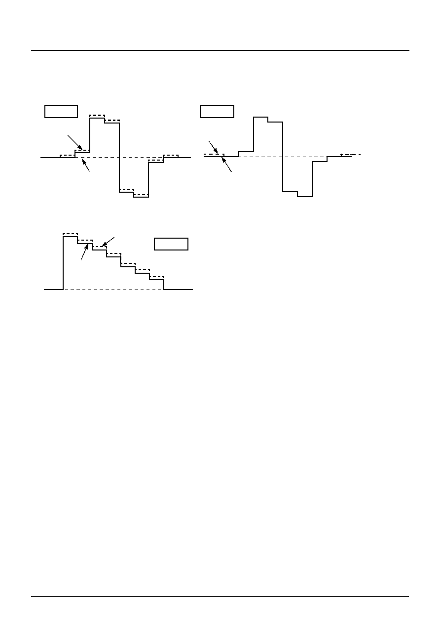
2.7.5. Wipe In/Wipe Out
With the wipe in/wipe out function it is possible to let
appear or disappear the complete inset picture starting
or ending at the corner of the inset picture position
defined by CPOS. Thereby the size of the visible pic-
ture-part is continuously increased and decreased
respectively. During this procedure the frame is shown
with its chosen widths. 3 different wipe in/out time peri-
ods or "no wipe" are programmable via WIPESP. The
wipe algorithm always works in horizontal and vertical
direction.
If WIPESP is set accordingly, PIPON controls the wipe
operation. When PIPON changes the wipe operation
starts. During this period, the readable PIPSTAT indi-
cates the ongoing wipe-process. A transition of PIPON
from `0' to `1' triggers the wipe-in. The wipe-in process
stops when the picture reaches its programmed size.
When PIPON changes from `1' to `0' the wipe-out
starts. The wipe-out is finished when the PIP picture
vanishes. Even for multi-picture display wipe operation
is possible. A change of PIPON or WIPESP during
wipe operation has only an effect after the wipe opera-
tion has been finished.
Fig. 2�12: Wipe Display
CPOS='01'
CPOS='10'
CPOS='11'
CPOS='00'
CPOS='01'
CPOS='10'
CPOS='11'
CPOS='00'
CPOS='01'
CPOS='10'
CPOS='11'
CPOS='00'
wipe in
wipe out
ADVANCE INFORMATION
PVP 9390A
Micronas
May 3, 2004; 6251-633-1AI
21
2.8. Output Signal Processing
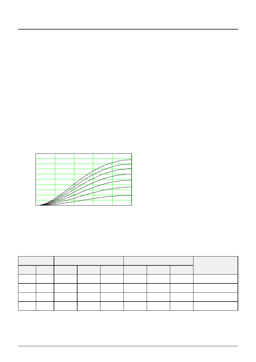
2.8.1. Luminance Peaking
To improve picture sharpness, a peaking filter which
amplifies higher frequencies of the input signal is
implemented. The amount of peaking can be varied in
seven steps by YPEAK. The setting `000' switches off
the peaking. The value `011' is recommended as this
value provides a good compromise between sharp-
ness impression and annoying aliasing. The character-
istic for all possible settings is shown in Fig. 2�13. The
emphasized frequency depends on the adjusted deci-
mation. The gain maximum is always located before
the band-limit ensuring optimal picture impression.
Peaking can be additionally increased by PKBOOST.
Coring should be switched on by YCOR to reduce
noise, which is also amplified when peaking is
enabled. As the coring stage is in front of the peaking
filter, 1 LSB noise will not be peaked.
2.8.2. RGB Matrix
The chip contains three different matrices, one suited
for EBU standards, one suited for NTSC-Japan and
one suited for NTSC-USA, which are selected via
MAT. The signal OUTFOR switches between YUV out-
put or RGB output. The signal UVPOLAR inverts the U
and V channels and results in Y-U-V output. The stan-
dard magnitudes and angles of the color-difference
signals in the UV-plane are defined as shown in
Table 2�16.
The color saturation can be adjusted with SATADJ
register in 16 steps between 0 and 1.875. Values
above 1.0 may clip the chrominance signals.
Fig. 2�13: Characteristics of Selectable Peaking Factors (0.5 = band limit)
0
0.1
0.2
0.3
0.4
0.5
0
1
2
3
4
5
6
7
8
9
10
normed frequency
gain [dB]
YPEAK = `000'
YPEAK = `001'
YPEAK = `010'
YPEAK = `011'
YPEAK = `100'
YPEAK = `101'
YPEAK = `110'
YPEAK = `111'
Table 2�16: RGB matrices characteristics
MAT
Magnitudes
Angles
Standard
D7
D6
(B-Y)
(R-Y)
(G-Y)
(B-Y)
(R-Y)
(G-Y)
0
0
2.028
1.14
0.7
0
90
236
EBU
0
1
2.028
1.582
0.608
0
95
240
NTSC (Japan)
1
0
2.028
2.028
0.608
0
105
250
NTSC (USA)
1
1
(Reserved)

PVP 9390A
ADVANCE INFORMATION
22
May 3, 2004; 6251-633-1AI
Micronas
2.8.3. Frame Generation And Colored Background
With FRWIDH and FRWIDV different to `0', a colored
frame is shown. With FRSEL a shaded frame is dis-
played
.
Note: If FRSEL is on, a shaded frame is shown, even if
FRWIDH and FRWIDV is `0'. Therefore, if no
frame is required, FRSEL as well as FRWIDH
and FRWIDV must be set to `0'.
The chip can display two different types of frames, one
simple monochrome frame and a more sophisticated
frame giving a three dimensional impression.
Fig. 2�14: Normal Frame and 3D Frame
The frame elements are always placed outside the
inset picture, except for the inner shade of three
dimensional frame or inner frame in multi-PIP mode.
There is no shift of the inset picture position if the inset
frame width is modified.
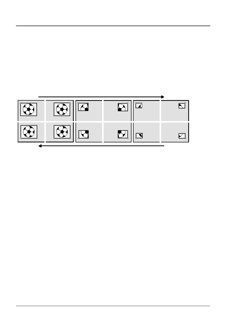
Fig. 2�15: Selectable Picture Configurations
A total of 4096 frame colors are programmable by FRY,
FRU, and FRV, 4 bits for each component. Horizontal
and vertical width of the frame are programmable inde-
pendently by FRWIDH and FRWIDV. If desired, frame
color is displayed over the whole PIP size or whole pic-
ture size of the main channel when PIPBG is set
accordingly. 64 background colors are programmable
by BGY, BGU, BGV, 2 bits for each component. Alter-
natively BGFRC sets the background to frame color.
2.8.4. 16:9 Inset Picture Support
To remove dark stripes at 16:9 inset pictures the verti-
cal display area is shrinkable with VPSRED. The num-
ber of omitted lines depends on the vertical decimation
factor.
.
Fig. 2�16: 16:9 Inset Picture without and with
Reduction of Vertical Picture Size
frame
no
frame color
background
no
background color
frame color
shades
no
dark/light
PiP Picture
background
picture
character
no
character
luminance
frame color
character background
transparent
char. background luminance
semi-transparent
Table 2�17: Number of lines with and without
reduction of vertical picture size
Vertical
Decimation
Factor
Displayed Lines
50 Hz
60 Hz
With
Without
Reduction
With
Without
Reduction
1
214
264
175
216
...
6
35 44
29
36
ADVANCE INFORMATION
PVP 9390A
Micronas
May 3, 2004; 6251-633-1AI
23
2.8.5. Parent Clock Generation
The phase of the output signals is locked to the rising
edge of the horizontal sync pulse. The frequency can
be varied in a certain range to ensure correct aspect
ratio for 16:9 applications depending on HZOOM. The
horizontal and vertical scaling can be used for all dis-
play frequencies.
2.8.6. Select Signal
For controlling an external RGB or YUV switch a select
signal is supplied. The delay of this signal is program-
mable for adaptation to different external output signal
processing devices (SELDEL).
Fig. 2�17: Select Timing
2.8.7. Automatic Brightness Reduction
Displaying a bright PIP picture, the beam current limi-
tation of the parent system may become active. This
may cause the parent picture to be influenced by the
inset picture. Therefore a detection circuit reduces the
brightness of the inset picture when the average
brightness is above a selectable threshold. After bright
picture content has disappeared, the initial brightness
reappears. The threshold is adjustable via ABRTHD
and the speed via ABRSPD. Both settings have to be
selected for parent system accordingly.
2.9. On Screen Display (OSD)
2.9.1. Display Format
The on screen display allows to insert a block of 5
characters into each of the PIP pictures. The charac-
ters are placed in a box (background) whose width is
64 pixels and height is 12 lines. This box is placed in
the upper left corner of the PIP picture. 64 different
characters are stored in a character ROM. Each char-
acter is defined by a pixel matrix consisting of 10 lines
and 12 pixels per line. A doubling of the character's
height and width is achieved by CHRDHW. The OSD
starting position is not influenced.
OSD display is also possible if PIP is switched off
(DISPMOD ='10010'). Now 3 lines of 20 characters
each are displayed at the PIP position.
Fig. 2�18: Example of OSD-only Mode
Fig. 2�19: Example of Transparent Mode (Normal and
Double Size OSD)
Table 2�18: Format conversion using HZOOM
Display
Format
In
set
Pi
c
t
ure
Format
De
si
red
P
I
P
Format
Re
quire
d P
a
rent
Freq
uen
c
y
Value of HZOOM
D2
D1
D0
4:3
4:3
4:3
27
0
0
0
4:3
4:3
16:9
20.25
0
0
1
16:9
4:3
4:3
36
0
1
0
16:9
16:9
16:9
36
0
1
0
SELDEL
PIP signal
OUTx
SEL
frame
picture
PVP 9390A
ADVANCE INFORMATION
24
May 3, 2004; 6251-633-1AI
Micronas
2.9.2. Character Programming
The characters are programmed via I�C bus using a
7 bit code which is identical with the ASCII code
except for some of the special characters. The codes
are stored in a character RAM consisting of 60 cells.
The character codes can be transmitted in two ways:
each character position can be addressed separately
by its 7 bit address or the characters can be written
consecutively starting at an arbitrarily chosen position.
In this case the address is increased automatically.
The 7 bit address consists of two parts: the 4 MSBs
are used to chose one of the partial pictures and the
3 LSBs to select one of the 5 characters per block.
2.9.3. Character and Character Background Color
The character's color is either same as frame color
(CHRFRC) or the character appears with a grey value
programmable with CHRY.
The character's background box is influenced by CHR-
BGON and CHRBGY. It can be made transparent so
that behind the characters the inset picture becomes
visible. Alternatively the semi-transparent mode can be
chosen. At this mode the background box contains the
original picture content with reduced luminance value.
This mode offers a good trade-off between reduction of
visible display area and character readability.
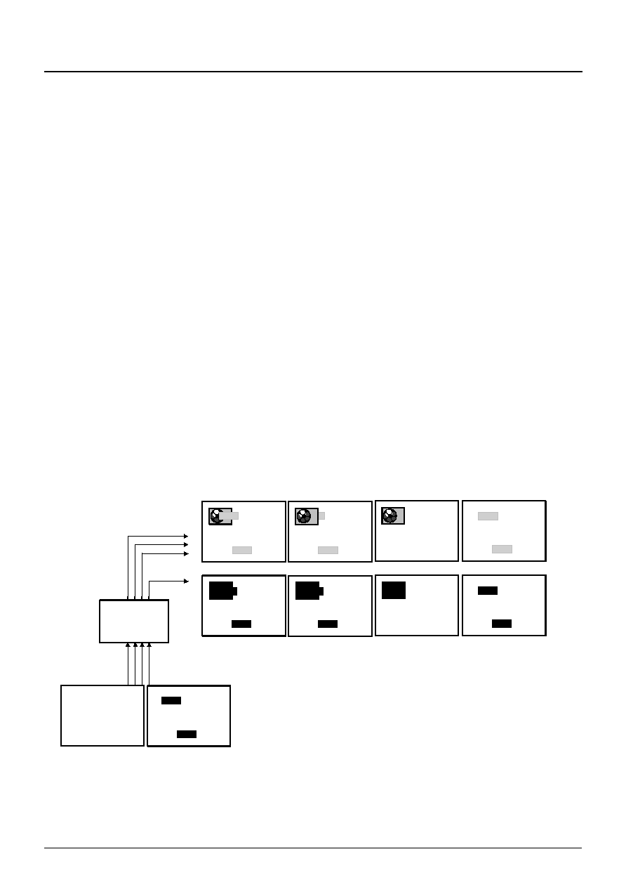
2.10. DA-Conversion And RGB/YUV Switch
The PVP 9390A includes three 7 bit DA-converters.
Brightness BRTADJ, Contrast CONADJ and overall
amplitude PKLR, PKLG, PKLB of the output signal
are adjustable. External RGB or YUV signals can be
connected to the inputs IN1...3. By forcing the FSW
input to high-level these signals are switched to the
outputs OUT1...3 while the internal signals are
switched off. The switch of YUV signals with sync on Y
is possible, if YSYNCOFS is set. The FSW input signal
is passed through to the SEL output. The setting of
RGBINS determines wether an RGB insertion is possi-
ble and which source, the external picture or the PIP,
gets priority. See Fig. 2�20.
The external RGB or YUV signals are each clamped to
the reference levels of the DACs to force uniform black
levels in each channel. The clamping needs careful
adjustment especially for VGA applications. The posi-
tion and the length of the blanking pulse as well as the
clamping pulse are adjustable (CLPPOS, CLPLEN). If
READD is set to `1' (100 Hz mode), all pulses are
shortened by one half. HZOOM influences the adjust-
ment range of the clamping and blanking pulse
because of the modified clock frequency, but the pulse
length is kept nearly constant.
Fig. 2�20: Visualization of RGB/YUV Insertion
OSD
RGB/VYU
R/V
G/Y
B/U
FSW
SEL
OSD
OSD
OSD
RGBINS='10'
PIPON='1'
RGBINS='00'
PIPON='1'
OSD
OSD
RGBIN='1X'
PIPON='0'
OSD
OSD
RGBINS='11'
PIPON='1'
IN
1
IN
2
IN
3
FS
W
S
E
L
OU
T
3
OU
T
2
OU
T
1
PVP 9390A

ADVANCE INFORMATION
PVP 9390A
Micronas
May 3, 2004; 6251-633-1AI
25
Fig. 2�21: PIP Horizontal Blanking Timing
2.10.1. Pedestal Level Adjustment
The pedestal level adjustment controlled by I�C signals
BLKLR, BLKLG, BLKLB enables the correction of
small offset errors, possibly appearing at the succes-
sive blanking stage of RGB processor. This adjustment
has an effect on the setup level during the active line
interval of each channel like the brightness adjustment
but has an enhanced resolution of 0.5 LSB. The maxi-
mum possible offset amounts to 7.5 LSBs. In YUV
mode (OUTFOR = `1') the action depends on the set-
ting of BLKINVR and BLKINVB. If BLKINVR (BLK-
INVB) is active the offset applies to the blank level of
the RV (BU) channel during the clamping interval for
shifting the setup level to the negative direction. In
RGB mode (OUTFOR = `0') BLKINVR and BLKINVB
have no effect.
2.10.2. Contrast, Brightness and Peak Level
Adjustment
The peak level adjustment modifies the magnitude of
each channel separately. It should be used to adapt
once the signal levels to the following stage. The con-
trast adjustment influences all three channels and
allows a further increase of 30 % of the peak level
magnitude. The effect of the brightness adjustment
depends on the selected output mode (RGB/YUV). In
YUV mode it changes the offset of the OUT2 (Y) signal
only while in RGB mode it changes the offset of all
three channels at the same time. The brightness
increase is up to 20 %.
BLANKP
HSP
CLAMPP
a
Parent
Video
allowed
HSP range
256 T
b
d
c
Table 2�19: PIP horizontal blanking timing examples
READD
CLPDEL
CLPLEN
a (
�
s)
Blanking
Start
b (
�
s)
Blanking
Duration
c (
�
s)
Clamping
Start
d (
�
s)
Clamping
Duration
D3
D2
D1
D0
D1
D0
0
0
0
0
0
0
-1.5
10.5
3
5
0
1
1
1
0
0
-11
10.5
-6.4
5
0
0
0
0
0
1
-1.5
7.9
2.2
3.8
0
1
1
1
0
1
-11.0
7.9
-7.3
3.8
1
0
0
0
0
0
-0.8
5.3
1.5
2.5
1
1
1
1
0
0
-5.5
5.3
-3.2
2.5
1
0
0
0
0
1
-0.8
4
1.1
1.9
1
1
1
1
0
1
-5.5
4
-3.6
1.9
PVP 9390A
ADVANCE INFORMATION
26
May 3, 2004; 6251-633-1AI
Micronas
Fig. 2�22: Pedestal Level Adjustment
64
OUTFOR = `1' (YUV Mode)
BLKLR = 0
BLKLR = 15
OUTFOR = `0' (RGB Mode)
0
BLKLR = 15
BLKLB = 15
BLKLB = 0
BLKLB = 15
BLKLG = 15
BLKLR = 0
BLKLB = 0
BLKLG = 0
BLKINVR = BLKINVB = `0'
64
BLKLR = 0
BLKLR = 15
BLKLB = 15
BLKLB = 0
BLKINVR = BLKINVB = `1'
OUT1, 3
OUT1, 3
OUT1 - 3

ADVANCE INFORMATION
PVP 9390A
Micronas
May 3, 2004; 6251-633-1AI
27
2.11. Data Slicer
Depending on SERVICE, Closed Caption data ("Line
21") or WSS (Wide-screen signalling) is sliced by the
digital data slicer and can be read out from I�C inter-
face. The line number of the sliced data is selectable
with SELLNR. Therefore WSS and CC can be pro-
cessed in different regions (e.g. CC with PAL M). The
Closed Caption data is assumed to conform with the
ITU standards EIA-608 and EIA-744-A. WSS data is
assumed to conform with ETS 300 294 (2nd edition,
May 1996).
2.11.1. Closed Caption
The closed caption data stream contains different data
services. In field 1 (line 21) the captions CC1 and CC2
and the text pages T1 and T2 are transmitted whereas
in field 2 (line 284) caption CC3, CC4, text T3, T4 and
the XDS data are transmitted. For more information
please refer to the above mentioned standards.
Raw CC as well as pre-filtered data is provided alter-
natively. With the built-in programmable XDS-Filter
(XDSCLS), the program rating information ("V-chip")
as well as others can be filtered out. The XDS filter
reduce traffic on the I�C bus and save calculation
power of the main controller. If no class filter is
selected, all incoming data (both fields) is sliced and
provided by the I�C interface. When one or more class
filters are chosen, only data in field 2 is sliced. Any
combination of class filters is allowed. Each "CLASS"
is divided into "TYPES" which can be sorted out by the
XDS-secondary filter (XDSTPE). Any combination of
type filter is allowed. Some type filter require an appro-
priate class filter.
2.11.2. Wide-screen Signalling (WSS)
In WSS mode (SERVICE='1') no filtering is possible.
All sliced data is passed to the output registers. In this
case XDSTPE selects the field number of the data to
be sliced. In Europe WSS carries for instance informa-
tion about aspect ratio and movie mode.
2.11.3. Indication of New Data
The sliced and possibly filtered data is available in
DATAA and DATAB. The corresponding status bits are
DATAV and SLFIELD. When new data were received,
DATAV becomes `1' and the controller must read
DATAA, DATAB and the status information. After both
data bytes were read DATAV becomes `0' until new
data arrives. It must be ensured that the data polling is
activated once per field (16.7 or 20 ms) or every sec-
ond field (33.3 or 40 ms), depending on the slicer con-
figuration and inset field frequency. The field number of
the data in DATAA and DATAB can be found in
SLFIELD. If one or more XDS-class filter are activated,
SLFIELD contains always `1'.
Additionally pin 10 (INT) may flag that new data is
received. Default this pin is in tri-state mode to be com-
patible with the Micronas SDA 9388X/9389X PIP
devices. It can also be configured by IRQCON to out-
put a single short pulse when new data is available or
behave equal to DATAV. In the last case the output
remains active until the two data registers DATAA/
DATAB are read. Both modes are useful to avoid con-
tinuos polling of the I�C bus. The microcontroller ini-
tiates I�C transfers only when required.
Fig. 2�23: Example in Pseudo-code for Reading the Data
while (1){
i2c_read pip_adr, status_reg_adr, status
if (status & data_valid_mask) {
i2c_read_inc pip_adr, dataa_reg_adr, dataa, datab, status
process_data dataa, datab, status
}
}

PVP 9390A
ADVANCE INFORMATION
28
May 3, 2004; 6251-633-1AI
Micronas
2.11.4. Violence Protection
The rating information is sent in the program rating
packet of the current (sometimes future) class in the
XDS data stream. If only this information is desired the
corresponding XDS filter (class 01h, type 05h) should
be used to suppress other data. The class/packet
bytes (0105h) precede the 2 Bytes rating information.
Each sequence is closed by the end-of-packet Byte
(0fh) and a checksum. This checksum complements
the Byte truncated sum of all Bytes to 00h. Except
comparison of the received rating with the adjusted
user rating threshold the microcontroller should check
the parity of each Byte and validate the checksum to
avoid misinterpretation of wrong received data.
The PVP 9390A offer some alternatives to blocking the
PIP channel completely by switching it off (see Fig. 2�
24).
The Mosaic mode (MOSAIC) hides details of the pic-
ture by reduced sharpness and increased aliasing.
The picture looks scrambled and is less perceptible.
Fig. 2�24: Possibilities of PIP Blocking
"Blue Screen"
"Mosaic"
"Warning Message"
THIS PROGRAM
CONTAINS VIOLENT
SCENES
ADVANCE INFORMATION
PVP 9390A
Micronas
May 3, 2004; 6251-633-1AI
29
2.12. Diagrams
Fig. 2�25: Display Mode 0 with Picture Sizes 1/4 and
1/9
Fig. 2�26: Display Mode 0 with Picture Sizes 1/16 and
1/36
Fig. 2�27: Display Mode 0 (with scaling) and Display
Mode 11
Fig. 2�28: Display Mode 2 and 3 (All Pictures with
Same Content)
Fig. 2�29: Display Modes 4 and 5
Fig. 2�30: Display Modes 6 and 7
Fig. 2�31: Display Modes 8 and 12
Fig. 2�32: Display Modes 9 and 10
0 1
2 3
0
1
0 1
0 1 2
0
1
2
0 1 2 3
0
1
2
3
0
1
2 3 4 5
0 1 2 3
4 5
PVP 9390A
ADVANCE INFORMATION
30
May 3, 2004; 6251-633-1AI
Micronas
Fig. 2�33: Display Modes 13 and 14
Fig. 2�34: Display Modes 15 and 16
Fig. 2�35: Display Modes 17 and 18
Fig. 2�36: Display Mode 20 (Double Window 1) and
19 (Double Window 1.5)
Fig. 2�37: Combination of Display Modes 17/18 and
9/10 (Dual PIP Application)
Fig. 2�38: Display Modes 19 and 20 (Dual PIP
Application)
0 1
2 3
4 5
6 7
8 9
10 11
0 1 2 3 4 5
6 7 8 9 10 11
0 1 2
3 4 5
6 7 8
0 1 2 3
4 5 6 7
8 9 10 11
0 1 2 3 4 5
6
7
8
9
10
0
1
2
3
4 5 6 7 8
ADVANCE INFORMATION
PVP 9390A
Micronas
May 3, 2004; 6251-633-1AI
31
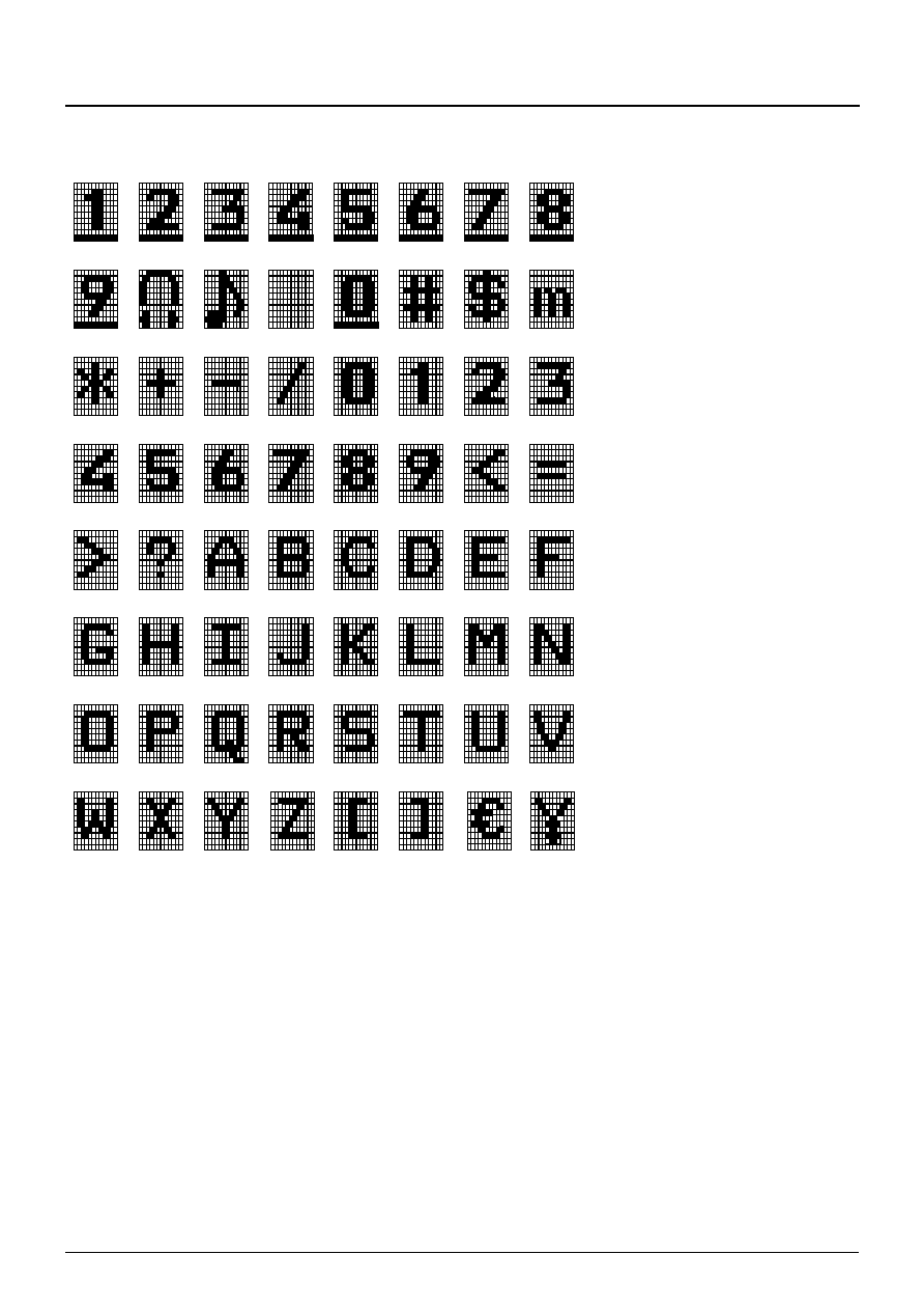
2.13. OSD Character Set
Fig. 2�39: OSD Character Set
1011010=5A
1011110=5E
1011111=5F
0001010=0A
0100000=20
0100001=21
0100100=24
0100101=25
0001011=0B
0101010=2A
0101011=2B
0101101=2D
0110000=30
0110001=31
0110010=32
0110011=33
0110100=34
0110101=35
0101111=2F
0110110=36
0111000=38
0111001=39
0111100=3C
0111101=3D
0110111=37
0111110=3E
1000001=41
1000010=42
1000011=43
1000100=44
1000101=45
1000110=46
0111111=3F
1000111=47
1001001=49
1001010=4A
1001011=4B
1001100=4C
1001101=4D
1001110=4E
1001000=48
1001111=4F
1010001=51
1010010=52
1010100=54
1010101=55
1010110=56
1010000=50
1010111=57
1011001=59
1011101=5D
1011000=58
1011011=5B
1010011=53
0100011=23
0000001=01
0000010=02
0000011=03
0000100=04
0000101=05
0000110=06
0001000=08
0001001=09
0000111=07
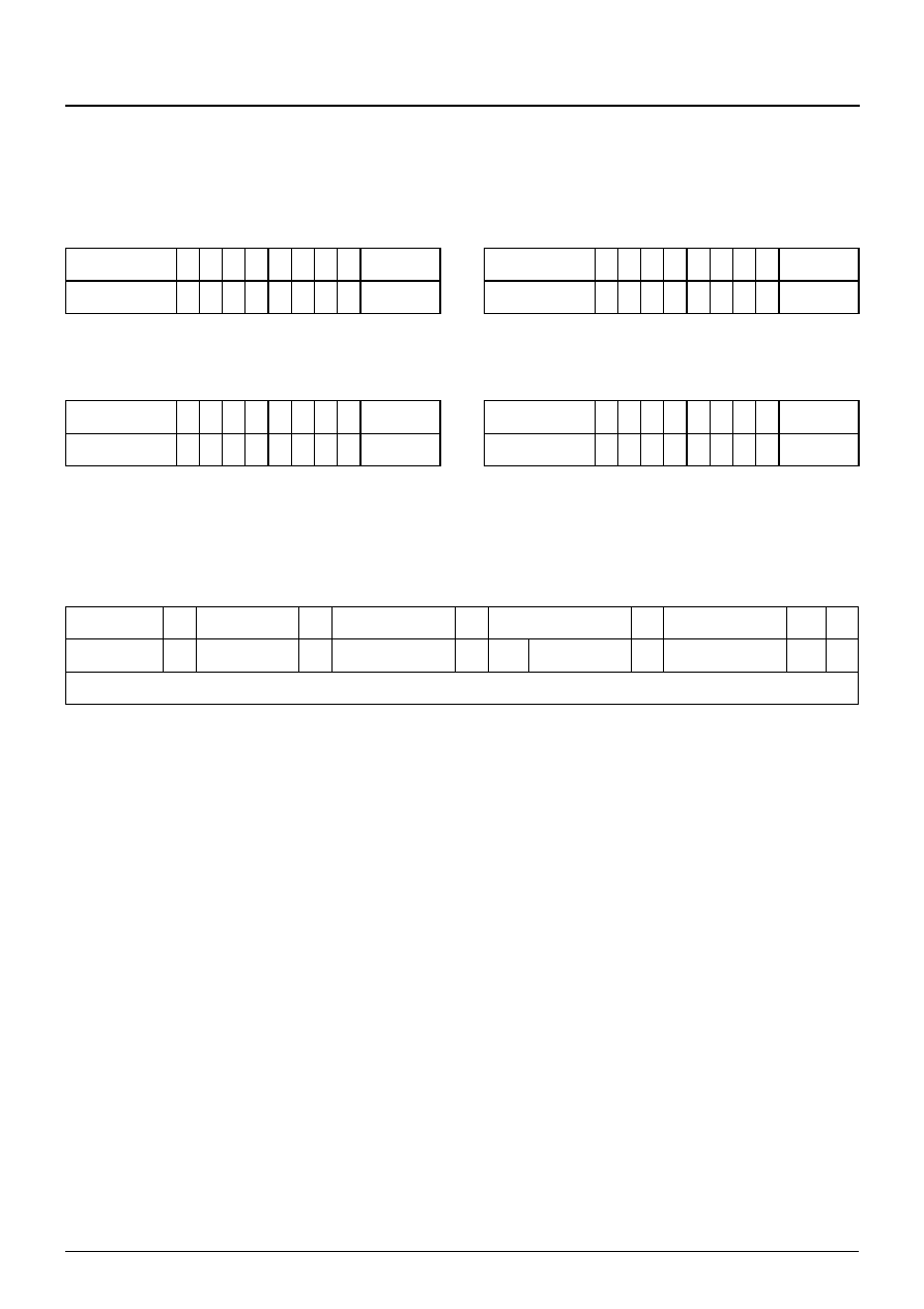
PVP 9390A
ADVANCE INFORMATION
32
May 3, 2004; 6251-633-1AI
Micronas
3. I
2
C Bus
3.1. I
2
C Bus Address
3.2. I
2
C Bus Format
Write operation is possible at registers 00h-21h and
2Eh-3Eh only, read operation is possible at registers
28h, 2Ah-2Ch, 3Fh only. An automatic address incre-
ment function is implemented.
Table 3�1: First address (I2C1= `0', I2C2= `0')
Write Address1 1
1
0
1
0
1
1
0
(D6h)
Read Address1 1
1
0
1
0
1
1
1
(D7h)
Table 3�2: Third address (I2C1= `0', I2C2= `1')
Write Address1 1
1
0
1
0
1
0
0
(D4h)
Read Address1 1
1
0
1
0
1
0
1
(D5h)
Table 3�3: Second address (I2C1= `1', I2C2= `0')
Write Address2 1
1
0
1
1
1
1
0
(DEh)
Read Address2 1
1
0
1
1
1
1
1
(DFh)
Table 3�4: Fourth address (I2C1= `1', I2C1= `1')
Write Address1 1
1
0
1
1
1
0
0
(DCh)
Read Address1 1
1
0
1
1
1
0
1
(DDh)
Table 3�5: I
2
C-bus format
WRITE
S
1101x110
A
Subaddress
A
Data Byte
A
****
A
P
READ
S
1101x110
A
Subaddress
A
Sr
1101x111
A
Data Byte n
NA
P
S: Start condition / Sr Repeated start condition / A: Acknowledge / P: Stop condition / NA: No Acknowledge
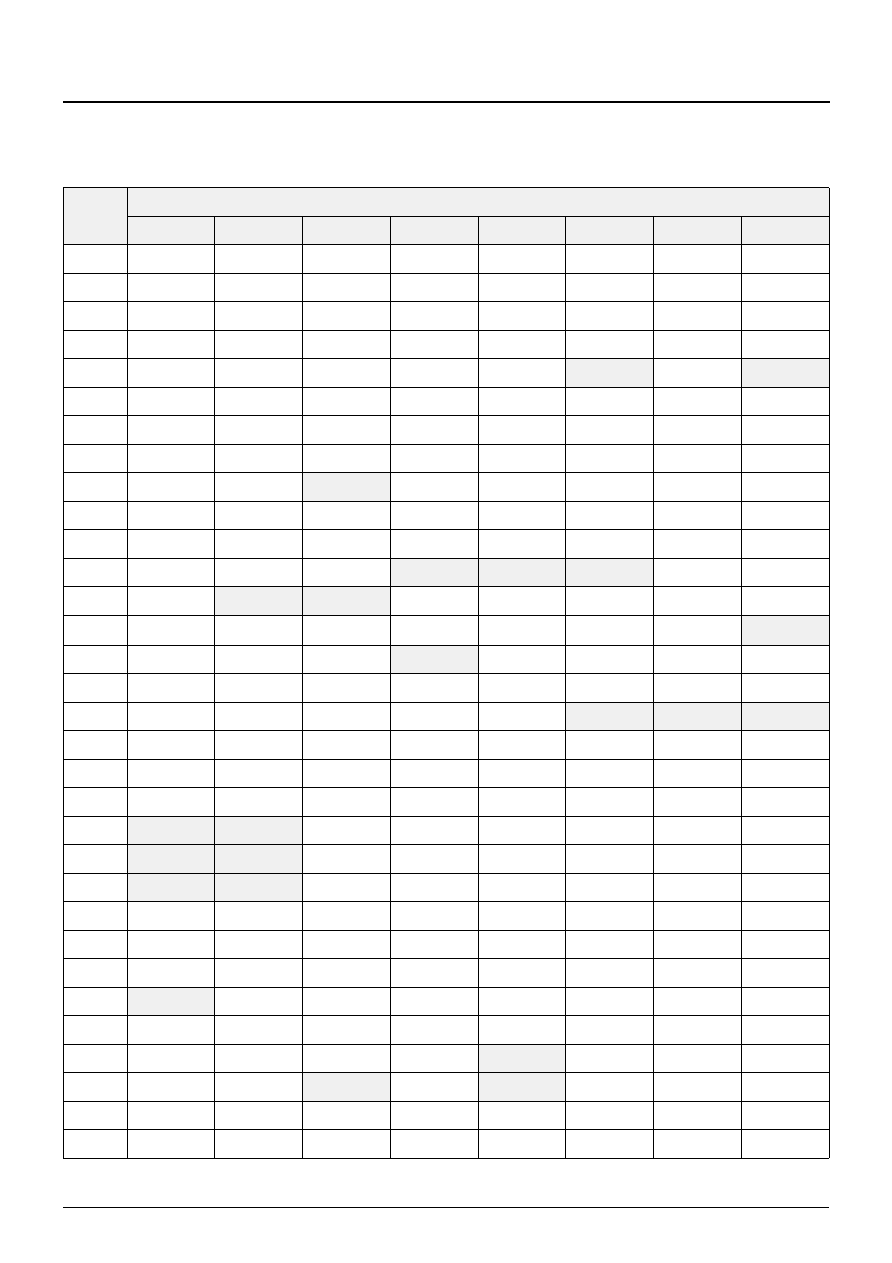
ADVANCE INFORMATION
PVP 9390A
Micronas
May 3, 2004; 6251-633-1AI
33
3.3. I
2
C Bus Command TableI
Table 3�6: I
2
C bus command table
Subadd
(Hex)
Data Byte
D7
D6
D5
D4
D3
D2
D1
D0
00h
PIPON
CPOS1
CPOS0
YUVSEL
READD
PROGEN
FIESEL1
FIESEL0
01h
POSHOR7
POSHOR6
POSHOR5
POSHOR4
POSHOR3
POSHOR2
POSHOR1
POSHOR0
02h
POSVER7
POSVER6
POSVER5
POSVER4
POSVER3
POSVER2
POSVER1
POSVER0
03h
VFP3
VFP2
VFP1
VFP0
HFP3
HFP2
HFP1
HFP0
04h
DISPSTD1
DISPSTD0
FREEZE
MOSAIC
SIZEHOR1
SIZEHOR0
SIZEVER1
SIZEVER0
05h
FPSTD1
FPSTD0
PIPBG1
PIPBG0
FMACTP
HZOOM2
HZOOM1
HZOOM0
06h
HSPINV
VSPINV
VSPNSRQ
VSPDEL4
VSPDEL3
VSPDEL2
VSPDEL1
VSPDEL0
07h
FRSEL
INFRM
VPSRED
FRWIDH2
FRWIDH1
FRWIDH0
FRWIDV1
FRWIDV0
08h
RGBINS1
RGBINS0
VERBLK
SELDOWN
SELDEL3
SELDEL2
SELDEL1
SELDEL0
09h
Set to 0
DISPMOD1
DISPMOD0
CLPDEL4
CLPDEL3
CLPDEL2
CLPDEL1
CLPDEL0
0Ah
AGCRES
AGCMD1
AGCMD0
AGCVAL3
AGCVAL2
AGCVAL1
AGCVAL0
NOSIGB
0Bh
CVBSEL1
CVBSEL0
CLMPID1
CLMPID0
BLKVCHYS
BLKVCVAL
LMOFST1
LMOFST0
0Ch
PLLITC1
PLLITC0
BLKVCFIL
(reserved)
YCDEL3
YCDEL2
YCDEL1
YCDEL0
0Dh
CSTAND2
CSTAND1
CSTAND0
CSTDEX1
CSTDEX0
(reserved)
CKILL1
CKILL0
0Eh
BGPOS
(reserved)
DEEMP1
DEEMP0
COLON
ACCFIX
CHRBW1
CHRBW0
0Fh
IFCOMP1
IFCOMP0
HUE5
HUE4
HUE3
HUE2
HUE1
HUE0
10h
SATNR
FMACTI
CPLLOF
SCADJ4
SCADJ3
SCADJ2
SCADJ1
SCADJ0
11h
CONADJ3
CONADJ2
CONADJ1
CONADJ0
BLKLR3
BLKLR2
BLKLR1
BLKLR0
12h
BRTADJ3
BRTADJ2
BRTADJ1
BRTADJ0
BLKLG3
BLKLG2
BLKLG1
BLKLG0
13h
TRIOUT
REFINT
BLKINVR
BLKINVB
BLKLB3
BLKLB2
BLKLB1
BLKLB0
14h
PKLR7
PKLR6
PKLR5
PKLR4
PKLR3
PKLR2
PKLR1
PKLR0
15h
PKLG7
PKLG6
PKLG5
PKLG4
PKLG3
PKLG2
PKLG1
PKLG0
16h
PKLB7
PKLB6
PKLB5
PKLB4
PKLB3
PKLB2
PKLB1
PKLB0
17h
MAT1
MAT0
BGY1
BGY0
FRY3
FRY2
FRY1
FRY0
18h
OUTFOR
UVPOLAR
BGU1
BGU0
FRU3
FRU2
FRU1
FRU0
19h
(reserved)
BGFRC
BGV1
BGV0
FRV3
FRV2
FRV1
FRV0
1Ah
SATADJ3
SATADJ2
SATADJ1
SATADJ0
YPEAK2
YPEAK1
YPEAK0
YCOR
1Bh
XDSCLS4
XDSCLS3
XDSCLS2
XDSCLS1
XDSCLS0
XDSTPE2
XDSTPE1
XDSTPE0
1Ch
UVSEQ
MPIPBG
SERVICE
SELLNR1
SELLNR0
IRQCON2
IRQCON1
IRQCON0
1Dh
(reserved)
(reserved)
PALIDL2
PALIDL1_1
PALIDL1_0
PIPBLK
(reserved)
PALIDL0
1Eh
POSOFV2
POSOFV1
POSOFV0
POSOFH4
POSOFH3
POSOFH2
POSOFH1
POSOFH0
1Fh
(reserved)
(reserved)
(reserved)
VSHRNK4
VSHRNK3
VSHRNK2
VSHRNK1
VSHRNK0

PVP 9390A
ADVANCE INFORMATION
34
May 3, 2004; 6251-633-1AI
Micronas
20h
(reserved)
(reserved)
(reserved)
HSHRNK4
HSHRNK3
HSHRNK2
HSHRNK1
HSHRNK0
21h
(reserved)
(reserved)
(reserved)
(reserved)
DWCOR
PKBOOST
CLPLEN1
CLPLEN0
22h
PIPHLT
ABRTHD3
ABRTHD2
ABRTHD1
ABRTHD0
ABRSPD2
ABRSPD1
ABRSPD0
23h
INFRMOD
DISPMOD6
DISPMOD5
DISPMOD4
DISPMOD3
DISPMOD2
WIPESP1
WIPESP0
24h
CZMEN
CZMSP1
CZMSP0
(reserved)
WRPOS3
WRPOS2
WRPOS1
WRPOS0
25h
CHRFRC
CHRDHW
CHRY1
CHRY0
CHRBGY1
CHRBGY0
CHRBGON1
CHRBGON0
26h
OSDON
CHRADR6
CHRADR5
CHRADR4
CHRADR3
CHRADR2
CHRADR1
CHRADR0
27h
CHRCLR
CHRCOD6
CHRCOD5
CHRCOD4
CHRCOD3
CHRCOD2
CHRCOD1
CHRCOD0
28h
FRMMD
PIPSTAT
SYSNCST1
SYSNCST0
CKSTAT
STDET2
STDET1
STDET0
29h
(reserved)
(reserved)
(reserved)
(reserved)
(reserved)
(reserved)
(reserved)
(reserved)
2Ah
DATAA7
DATAA6
DATAA5
DATAA4
DATAA3
DATAA2
DATAA1
DATAA0
2Bh
DATAB7
DATAB6
DATAB5
DATAB4
DATAB3
DATAB2
DATAB1
DATAB0
2Ch
PALDET
(reserved)
DEVICE1
DEVICE0
PRNSTD
PALID
DATAV
SLFIELD
2Dh
(reserved)
(reserved)
(reserved)
(reserved)
(reserved)
(reserved)
(reserved)
(reserved)
2Eh
SCMREL1
SCMREL0
SCMIDL2
SCMIDL1
SCMIDL0
SCCDIV
(reserved)
BELLIIR
2Fh
PALINC1
PALINC2
LOCKSP1
LOCKSP0
SECACCL2
SECACCL1
SECACCL0
SECACC
30h
ADLCK
ADLCKSEL
ADLCKCC
CLRANGE1
CLRANGE0
NADJ2
NADJ1
NADJ0
31h
NSRED2
NSRED1
NSRED0
SLLTHD1
SLLTHD0
ISHFT1
ISHFT0
ENLIM
32h
DETECT5060
VTHRL50_6
VTHRL50_5
VTHRL50_4
VTHRL50_3
VTHRL50_2
VTHRL50_1
VTHRL50_0
33h
BCOROFF
VTHRL60_6
VTHRL60_5
VTHRL60_4
VTHRL60_3
VTHRL60_2
VTHRL60_1
VTHRL60_0
34h
VTHRH50_3
VTHRH50_2
VTHRH50_1
VTHRH50_0
VTHRH60_3
VTHRH60_2
VTHRH60_1
VTHRH60_0
35h
CLMPSTGY
SLLTHDVP
SLLTHDV2
SLLTHDV1
SLLTHDV0
VFLYWHLMD1 VFLYWHLMD0 VFLYWHL
36h
FLNSTRD1
FLNSTRD0
CLMPCHARY1 CLMPCHARY0 VDETIFS
VDETITC
VLP1
VLP0
37h
LATENCY1
LATENCY0
FILTBRST
CLMPIST4
CLMPIST3
CLMPIST2
CLMPIST1
CLMPIST0
38h
(reserved)
(reserved)
(reserved)
CLKP_INV
INCRSEL
FINECLMP
INSEL_1
INSEL_0
39h
DTOINCR_7
DTOINCR_6
DTOINCR_5
DTOINCR_4
DTOINCR_3
DTOINCR_2
DTOINCR_1
DTOINCR_0
3Ah
(reserved)
(reserved)
(reserved)
GPO_2
GPO_1
GPO_0
GPOEN
CLKOUTEN
3Bh
(reserved)
(reserved)
(reserved)
(reserved)
(reserved)
(reserved)
(reserved)
YSYNCOFS
3Ch
(reserved)
(reserved)
AFIL_OFF
STBY_REF
STBY_OTA
STBY_ADC1
STBY_ADC2
STBY_ADC3
3Dh
STBY_BUFFE
R
STBY_CLAMP STBY_DAC1
STBY_DAC2
STBY_DAC3
STBY_GAIN
STBY_OFFSE
T
STBY_REF
3Eh
TRIM_BGP_7
TRIM_BGP_6
TRIM_BGP_5
TRIM_BGP_4
TRIM_BGP_3
TRIM_BGP_2
TRIM_BGP_1
TRIM_BGP_0
3Fh
(reserved)
(reserved)
(reserved)
(reserved)
(reserved)
(reserved)
PVPREV_1
PVPREV_0
Grey shading = After power on, the grey marked data bits are set to '1', all other to `0`
Table 3�6: I
2
C bus command table, continued
Subadd
(Hex)
Data Byte
D7
D6
D5
D4
D3
D2
D1
D0

ADVANCE INFORMATION
PVP 9390A
Micronas
May 3, 2004; 6251-633-1AI
35
3.4. I
2
C Bus Command Description
Subaddress 00h
Table 3�7: PIPON
PIPON
PIP On:
Switches the PIP insertion on
D7
0
PIP insertion off
1
PIP insertion on
Table 3�8: CPOS
CPOS
Coarse Position:
Coarse position of the picture
D6
D5
0
0
Upper left position
0
1
Upper right position
1
0
Lower left position
1
1
Lower right position
Table 3�9: YUVSEL
YUVSEL
YUV Select:
Selects YUV mode
D4
0
CVBS or Y/C source
1
YUV source
Table 3�10: READD
READD
Read Double Mode:
Double read frequency for compatibility with systems that use 2fH (e.g.100 Hz, progressive)
D3
0
PIP display with single read frequency and 2x oversampling
1
PIP display with double read frequency

PVP 9390A
ADVANCE INFORMATION
36
May 3, 2004; 6251-633-1AI
Micronas
Subaddress 01h
Subaddress 02h
Table 3�11: PROGEN
PROGEN
Progressive Scan Enable:
For compatibility with progressive scan systems
D2
0
Each line of PIP is read once (normal operation)
1
Each line of PIP is read twice (line doubling operation)
Table 3�12: FIESEL
FIESEL
Field Select:
Set field or frame display mode
D1
D0
0
0
Frame mode (if possible)
0
1
Field mode (first field only)
1
0
Field mode (second field only)
1
1
Field mode (one of both)
Table 3�13: POSHOR
POSHOR
Horizontal Picture Position:
Horizontal position adjustment of the PIP in steps of 4 pixel shift direction depends on the
coarse positioning of the picture
D7-D0
Table 3�14: POSVER
POSVER
Vertical Picture Position:
Vertical position adjustment of the PIP in steps of 1 lines shift direction depends on the coarse
positioning of the picture
D7-D0
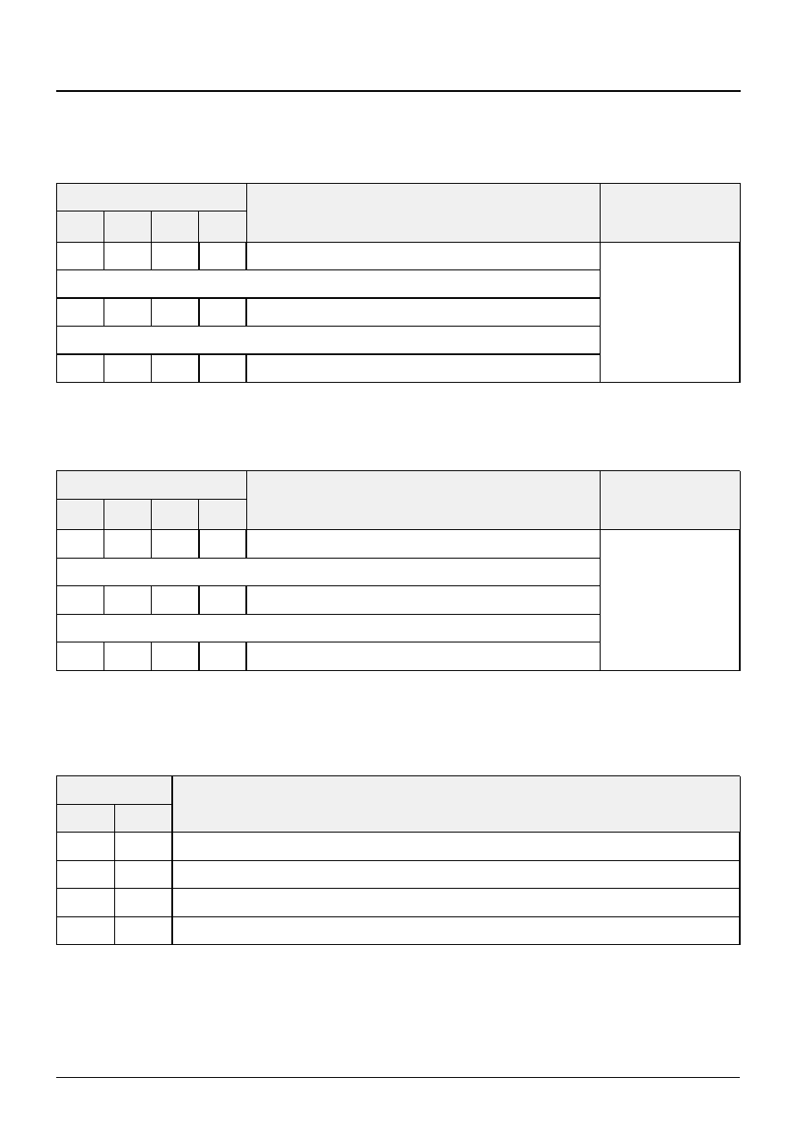
ADVANCE INFORMATION
PVP 9390A
Micronas
May 3, 2004; 6251-633-1AI
37
Subaddress 03h
Subaddress 04h
Table 3�15: HFP
HFP
Horizontal Fine Positioning:
Changes the position of the horizontal acquisition window
by steps of 2 pixel
Note
D3
D2
D1
D0
1
0
0
0
-16 pixel (-0.8
�
s), most right position of the image
Values refer to the
undecimated picture
...
0
0
0
0
0 pixel, nominal center position
...
0
1
1
1
+14 pixel (0.7
�
s), most left position
Table 3�16: VFP
VFP
Vertical Fine Positioning:
Changes the position of the vertical acquisition window
by steps of 1 line
Note
D7
D6
D5
D4
1
0
0
0
-
8 lines, most upper position of the image
Values refer to the
undecimated picture
...
0
0
0
0
0 lines, nominal center position
...
0
1
1
1
+7 lines, most lower position
Table 3�17: DISPSTD
DISPSTD
Display Standard:
Selects the line standard of PIP display
D7
D6
0
0
PIP depends on detected parent standard (multi PIP) or inset standard (single PIP)
0
1
PIP display is always in 625 line mode
1
0
PIP display is always in 525 line mode
1
1
Freeze last detected display standard and size
PVP 9390A
ADVANCE INFORMATION
38
May 3, 2004; 6251-633-1AI
Micronas
Table 3�18: FREEZE
FREEZE
Freeze Picture:
Interrupts the inset picture writing and displays still picture
D5
0
Live picture
1
Still picture
Table 3�19: MOSAIC
MOSAIC
Mosaic Mode:
Hides picture details, intended for use with parental control
D4
0
Mosaic mode off
1
Mosaic mode on
Table 3�20: SIZEHOR
SIZEHOR
Horizontal Size:
Horizontal decimation
D3
D2
0
0
Reduction = 2
0
1
Reduction = 3
1
0
Reduction = 4
1
1
Reduction = 6
Table 3�21: SIZEVER
SIZEVER
Vertical Size:
Vertical decimation
D1
D0
0
0
Reduction = 2
0
1
Reduction = 3
1
0
Reduction = 4
1
1
Reduction = 6
ADVANCE INFORMATION
PVP 9390A
Micronas
May 3, 2004; 6251-633-1AI
39
Subaddress 05h
Table 3�22: FPSTD
FPSTD
Force Parent Standard:
Forces the parent standard to one of the following modes
D7
D6
0
0
Auto-detect parent standard
0
1
50 Hz/625 lines parent standard forced
1
0
60 Hz/525 lines parent standard forced
1
1
Freeze last detected standard
Table 3�23: PIPBG
PIPBG
PIP Background Display:
Selects the background display
D5
D4
0
0
PIP visible, no background display
0
1
PIP invisible, background display in PIP
1
0
PIP visible, full screen background display
1
1
PIP invisible, background display in PIP and full screen background
Table 3�24: FMACTP
FMACTP
Frame Mode Activation Parent:
Selects the parent condition for the activation of the frame mode
D3
0
Frame mode active for standard parent video sources only
1
Frame mode active for some nonstandard sources also
Table 3�25: HZOOM
HZOOM
Horizontal Zoom:
Selects the parent (display) clock frequency
D2
D1
D0
0
0
0
27.34 MHz
0
0
1
20.25 MHz
0
1
0
35.27 MHz
PVP 9390A
ADVANCE INFORMATION
40
May 3, 2004; 6251-633-1AI
Micronas
Subaddress 06h
0
1
1
25.43 MHz
1
0
0
26.67 MHz
1
0
1
20.63 MHz
1
1
0
34.17 MHz
1
1
1
28.04 MHz
Table 3�25: HZOOM, continued
HZOOM
Horizontal Zoom:
Selects the parent (display) clock frequency
D2
D1
D0
Table 3�26: HSPINV
HSPINV
Horizontal Sync Pulse Inversion:
Inverts the polarity of HSP
D7
0
No inversion, raising edge is sync reference
1
HSP inverted, falling edge is sync reference
Table 3�27: VSPINV
VSPINV
Vertical Sync Pulse Inversion:
Inverts the polarity of VSP
D6
0
No inversion, raising edge is sync reference
1
VSP inverted, falling edge is sync reference
Table 3�28: VSPNSRQ
VSPNSRQ
Vertical Sync Pulse Noise Reduction:
Activates automatic V insertion that generates vertical sync pulses in case of missing external
VSP
D5
0
On
1
Off
ADVANCE INFORMATION
PVP 9390A
Micronas
May 3, 2004; 6251-633-1AI
41
Subaddress 07h
Table 3�29: VSPDEL
VSPDEL
Vertical Sync Pulse Delay:
Delay of the vertical sync pulse in steps of
128 parent clocks
Note
D4
D3
D2
D1
D0
0
0
0
0
0
No delay (0)
Delay depends on
HZOOM
...
1
1
1
1
1
Maximum delay, 4096 clocks of parent fre-
quency
Table 3�30: FRSEL
FRSEL
Frame Select:
Selects between the normal frame and the shaded frame
D7
0
Normal frame
1
Shaded frame with 3D impression
Table 3�31: INFRM
INFRM
Inner Frame Activation:
Actives inner frame (4 pixel width, 2 lines height) for multi-PIP display)
D6
0
Inner frame off
1
Inner frame on
Table 3�32: VPSRED
VPSRED
Vertical Picture Size Reduction:
Reduces vertical picture size to suppress black bars in 16:9 programs
D5
0
No reduction
1
Reduction on
PVP 9390A
ADVANCE INFORMATION
42
May 3, 2004; 6251-633-1AI
Micronas
Subaddress 08h
Table 3�33: FRWIDH
FRWIDH
Frame Width Horizontal:
Adjusts the horizontal width of the PIP frame in steps of one pixel
D4
D3
D2
0
0
0
No horizontal frame
...
1
1
1
7 pixel
Table 3�34: FRWIDV
FRWIDV
Frame Width Vertical:
Adjusts the vertical width of the PIP frame in steps of one line
D1
D0
0
0
No vertical frame
...
1
1
3 lines
Table 3�35: RGBINS
RGBINS
RGB Insertion:
Controls the insertion of external RGB/YUV sources
D7
D6
0
0
No external insertion possible, FSW input inactive
0
1
External insertion forced (FSW = 1)
1
0
External insertion with FSW possible (priority of FSW input)
1
1
External insertion with FSW possible (priority of PIP)
Table 3�36: VERBLK
VERBLK
Vertical Blanking:
Switches the vertical blanking mode
D5
0
Blanking level at DAC outputs only during line-blanking intervals
1
Blanking level at DAC outputs during line-blanking intervals and field-blanking intervals, 16
lines following the parent vertical synchronization pulse are blanked
ADVANCE INFORMATION
PVP 9390A
Micronas
May 3, 2004; 6251-633-1AI
43
Subaddress 09h
Table 3�37: SELDOWN
SELDOWN
Select Down:
Switches the driver type at the output of the SEL pin
D4
0
Open source output
1
TTL output
Table 3�38: SELDEL
SELDEL
Select Delay:
Adjusts the delay of select signal
D3
D2
D1
D0
1
0
0
0
-
8 clock periods of display clock
...
0
0
0
0
0 clock periods of display clock
...
0
1
1
1
+7 clock cycles of display clock
Table 3�39: DISPMOD
DISPMOD
Display Mode:
Selects display modes with equal pictures
D6
D5
0
0
Single PIP mode
0
1
3 x1/9 PIP (same content)
1
0
4 x1/16 PIP (same content)
1
1
(Reserved)

PVP 9390A
ADVANCE INFORMATION
44
May 3, 2004; 6251-633-1AI
Micronas
Subaddress 0Ah
Table 3�40: CLPDEL
CLPDEL
Clamping Delay:
Delay of the clamping pulse for the external RGB/YUV inputs in steps of
8 parent clock periods
D4
D3
D2
D1
D0
0
0
0
0
0
No delay (0)
...
1
1
1
1
1
Maximum delay, 256 clock periods of parent frequency
Table 3�41: AGCRES
AGCRES
Automatic Gain Control Reset:
Resets AGC
D7
0
Normal operation
1
Reset of AGC
Table 3�42: AGCMD
AGCMD
AGC Mode:
Controls the AGC operation
D6
D5
0
0
Evaluation of sync height and ADC overflow
0
1
Evaluation of sync height only
1
0
Evaluation of ADC overflow only
1
1
AGC fixed (gain depends on AGCVAL)
ADVANCE INFORMATION
PVP 9390A
Micronas
May 3, 2004; 6251-633-1AI
45
Subaddress 0Bh
Table 3�43: AGCVAL
AGCVAL
Automatic Gain Control Value:
AGC value for fixed mode (AGCMD='11')
D4
D3
D2
D1
0
0
0
0
Input voltage 0.5 Vpp
...
1
0
0
0
Input voltage 1 Vpp
...
1
1
1
1
Input voltage 1.5 Vpp
Table 3�44: NOSIGB
NOSIGB
No Signal Behavior:
Controls behavior if synchronization is not possible (no source applied)
D0
0
Noisy picture
1
Colored background
Table 3�45: CVBSEL
CVBSEL
CVBS Select:
Select CVBS source
D7
D6
0
0
CVBS1
0
1
CVBS2
1
0
Y/C (Y@CVBS2 / C@CVBS3)
1
1
CVBS3
PVP 9390A
ADVANCE INFORMATION
46
May 3, 2004; 6251-633-1AI
Micronas
Table 3�46: CLMPID
CLMPID
Clamping Duration:
Adjusts duration of clamping pulse for ADC (inset channel)
D5
D4
0
0
1.28
�
s
0
1
1.77
�
s
1
0
2.27
�
s
1
1
2.96
�
s
Table 3�47: BLKVCHYS
BLKVCHYS
Blankvalue Hysteresis:
Blankvalue generation ... (sync-tip clamping only)
D3
0
Without hysteresis
1
With hysteresis
Table 3�48: BLKVCVAL
BLKVCVAL
Clamping Correction Offset:
(Back-porch clamping only)
D2
0
0
1
-1
Table 3�49: LMOFST
LMOFST
Luminance Offset:
Modifies black to blank level offset
D1
D0
0
0
No offset
0
1
Offset of 16 LSB
1
0
Offset of
-
8 LSB
1
1
Offset of
-
16 LSB
ADVANCE INFORMATION
PVP 9390A
Micronas
May 3, 2004; 6251-633-1AI
47
Subaddress 0Ch
Table 3�50: PLLITC
PLLITC
Inset PLL Time Constant:
Switches the time constant of the inset PLL
D7
D6
0
0
VCR1 (very fast)
0
1
VCR2
1
0
TV1
1
1
TV2 (very slow)
Table 3�51: BLKVCFIL
BLKVCFIL
Blankvalue Filtering:
(Sync-tip clamping only)
D5
0
Lowpass filter off
1
Lowpass filter on
Table 3�52: YCDEL
YCDEL
Y/C Delay:
Adjusts the delay between luminance and chrominance
D3
D2
D1
D0
1
0
0
0
-
8 pixel (
-
0.4
�
s with respect to undecimated picture)
...
0
0
0
0
0 pixel
...
0
1
1
1
+7 pixel (0.35
�
s)
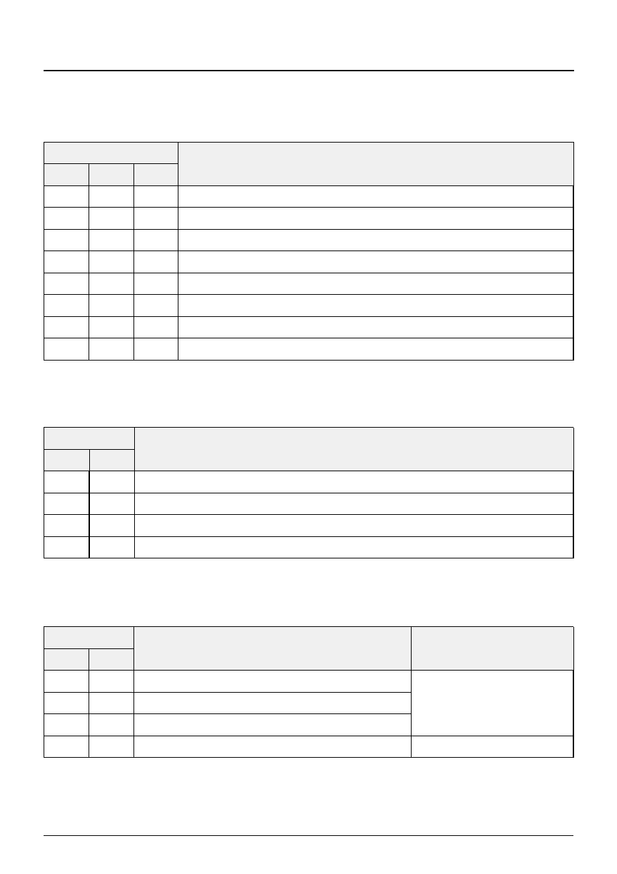
PVP 9390A
ADVANCE INFORMATION
48
May 3, 2004; 6251-633-1AI
Micronas
Subaddress 0Dh
Table 3�53: CSTAND
CSTAND
Color Standard:
Forces the desired color standard
D7
D6
D5
0
0
0
Automatic standard identification
0
0
1
NTSC-M
0
1
0
PAL-N (Argentina)
0
1
1
PAL-M
1
0
0
NTSC44
1
0
1
PAL-B/G/H/I/D
1
1
0
SECAM
1
1
1
PAL60
Table 3�54: CSTDEX
CSTDEX
Color Standard Exclusion:
Excludes standards from automatic standard identification
D4
D3
0
0
Ignore PAL-M / PAL-N
0
1
Ignore SECAM, PAL B/G, PAL60, NTSC4.4
1
0
Ignore PAL-M /PAL-N / NTSC-M
1
1
Ignore PAL-M / PAL-N / NTSC4.4 / PAL60
Table 3�55: CKILL
CKILL
Color Killer Threshold:
Damping of color carrier to switch color off
Note
D1
D0
0
0
-
30 dB
Only valid if color killer active
(COLON='0'),
Values are approximative
0
1
-
18 dB
1
0
-
24 dB
1
1
Color always off
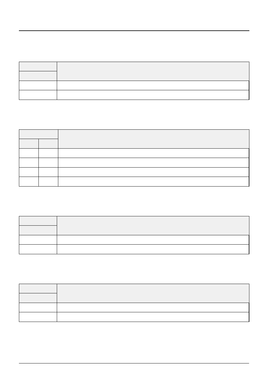
ADVANCE INFORMATION
PVP 9390A
Micronas
May 3, 2004; 6251-633-1AI
49
Subaddress 0Eh
Table 3�56: BGPOS
BGPOS
Burst Gate Position:
Adjusts position of burst gate (SECAM only)
D7
0
Normal position
1
0.5
�
s delayed
Table 3�57: DEEMP
DEEMP
Deemphase Selection:
Adjusts SECAM deemphase filter
D5
D4
0
0
Filter1
0
1
ITU recommendation
1
0
Filter2
1
1
Filter3
Table 3�58: COLON
COLON
Color On:
Disable color killer
D3
0
Color killer active
1
Color forced on
Table 3�59: ACCFIX
ACCFIX
Disable Automatic Chroma Control:
Disables the automatic chroma control (ACC)
D2
0
ACC active
1
ACC fixed (ACC set to nominal value)
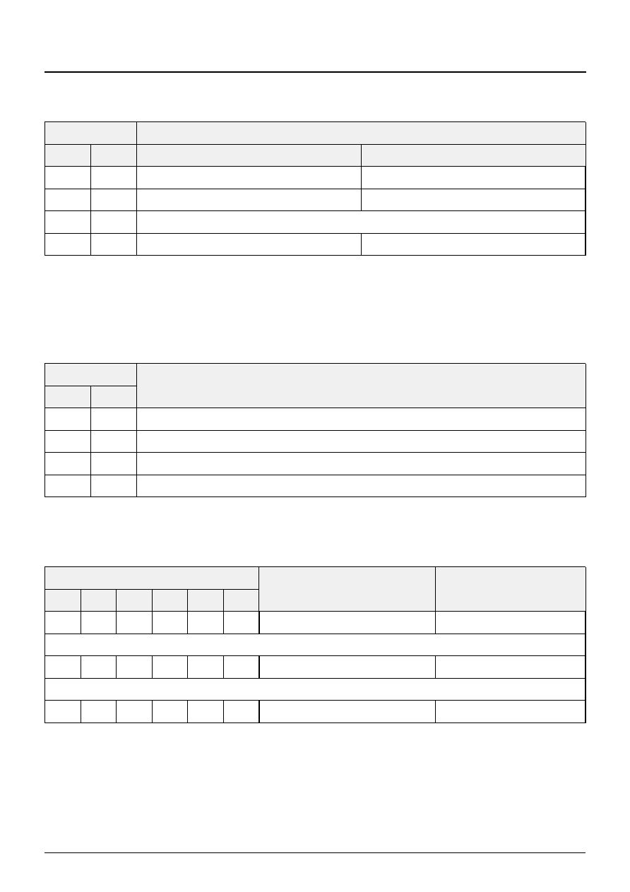
PVP 9390A
ADVANCE INFORMATION
50
May 3, 2004; 6251-633-1AI
Micronas
Subaddress 0Fh
Table 3�60: CHRBW
CHRBW
Chroma Bandwidth
D1
D0
PAL
SECAM
0
0
Wide
Small
0
1
Medium
Medium
1
0
Reserved
1
1
Small
Wide
Table 3�61: IFCOMP
IFCOMP
IF-Compensation Filter:
Equalizes the IF-stage characteristic
D7
D6
0
0
No filtering
0
1
Chroma bandpass active
1
0
IF-compensation bandpass (6 dB/octave)
1
1
Reserved
Table 3�62: HUE
HUE
Hue Control:
Phase of color subcarrier for NTSC
Note
D5
D4
D3
D2
D1
D0
1
0
0
0
0
0
-
44.8 �
Skin color becomes greenish
...
0
0
0
0
0
0
0�
...
0
1
1
1
1
1
43.4 �
Skin color becomes redish
ADVANCE INFORMATION
PVP 9390A
Micronas
May 3, 2004; 6251-633-1AI
51
Subaddress 10h
Table 3�63: SATNR
SATNR
Satellite Noise Reduction:
Stabilizes the horizontal PLL for bad satellite signals ("fishes")
D7
0
Disabled
1
Enabled
Table 3�64: FMACTI
FMACTI
Frame Mode Activation Inset:
Sets the inset condition for the activation of the frame mode
D6
0
Frame mode only active for standard inset video sources
1
Enhanced frame mode activation range
Table 3�65: CPLLOF
CPLLOF
Chroma PLL Off:
Opens loop of chroma PLL (only for test and servicing)
D5
0
Chroma PLL active
1
Chroma PLL opened (free running oscillator)
Table 3�66: SCADJ
SCADJ
Color Subcarrier Adjustment:
Color subcarrier frequency fine adjustment
D4
D3
D2
D1
D0
0
0
0
0
0
Max. negative deviation (
-
150 ppm)
...
0
0
1
1
1
Default (for nominal crystal frequency
...
1
1
1
1
1
Max. positive deviation (+310 ppm)
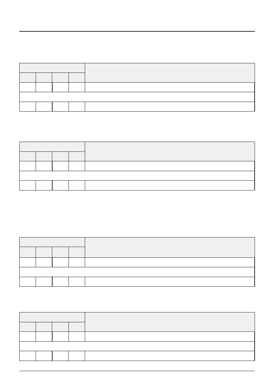
PVP 9390A
ADVANCE INFORMATION
52
May 3, 2004; 6251-633-1AI
Micronas
Subaddress 11h
Subaddress 12h
Table 3�67: CONADJ
CONADJ
Contrast Adjustment:
Adjusts the contrast of the picture, acts on OUT1-OUT3
D7
D6
D5
D4
0
0
0
0
Nominal contrast
...
1
1
1
1
+30 % contrast increase
Table 3�68: BLKLR
BLKLR
Blanking Level Red:
Adjusts the pedestal level of the OUT1 channel in steps of 0.5 LSB
D3
D2
D1
D0
0
0
0
0
No pedestal
...
1
1
1
1
+7.5 LSB offset
Table 3�69: BRTADJ
BRTADJ
Brightness Adjustment:
Adjusts the brightness of the picture, acts on OUT1-OUT3 in RGB mode
(YUVFOR = `0') and on OUT1 in YUV mode (YUVFOR = `1')
D7
D6
D5
D4
0
0
0
0
Nominal brightness
...
1
1
1
1
+20 % brightness increase
Table 3�70: BLKLG
BLKLG
Blanking Level Green:
Adjusts the pedestal level of the OUT2 channel in steps of 0.5 LSB
D3
D2
D1
D0
0
0
0
0
No pedestal
...
1
1
1
1
+7.5 LSB offset

ADVANCE INFORMATION
PVP 9390A
Micronas
May 3, 2004; 6251-633-1AI
53
Subaddress 13h
Table 3�71: TRIOUT
TRIOUT
Tri-state Output:
Sets OUT1-OUT3 to tristate mode (high resistance)
D7
0
Normal operation, outputs are active
1
Pins OUT1-3 are in tri-state mode
Table 3�72: REFINT
REFINT
Refresh Intervall:
Changes the refresh rate of eDRAM
Note
D6
0
Normal refresh
Keep it at `0'
1
Fast refresh
Table 3�73: BLKINVR
BLKINVR
Blanking Inversion Red:
Inverts the sign of the OUT1 channel offset (BLKLR)
D5
0
Offset added during the active picture
1
Offset added during blanking
Table 3�74: BLKINVB
BLKINVB
Blanking Inversion Blue:
Inverts the sign of the OUT3 channel offset (BLKLB)
D4
0
Offset added during the active picture
1
Offset added during blanking
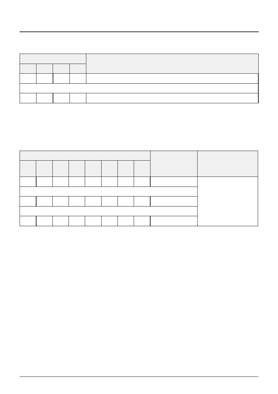
PVP 9390A
ADVANCE INFORMATION
54
May 3, 2004; 6251-633-1AI
Micronas
Subaddress 14h
Table 3�75: BLKLB
BLKLB
Blanking Level Blue:
Adjusts the pedestal level of the OUT3 channel in steps of 0.5 LSB
D3
D2
D1
D0
0
0
0
0
No pedestal
...
1
1
1
1
+7.5 LSB offset
Table 3�76: PKLR
PKLR
Peak Level Red:
Peak to peak output
voltage of the OUT1
channel
Note
D7
D6
D5
D4
D3
D2
D1
D0
0
0
0
0
0
0
0
0
0.3 V
pp
Values refer to contrast
(CONADJ) and bright-
ness (BRTADJ) at mini-
mum
...
1
1
0
0
0
0
0
0
1 V
pp
...
1
1
1
1
1
1
1
1
1.2 V
pp
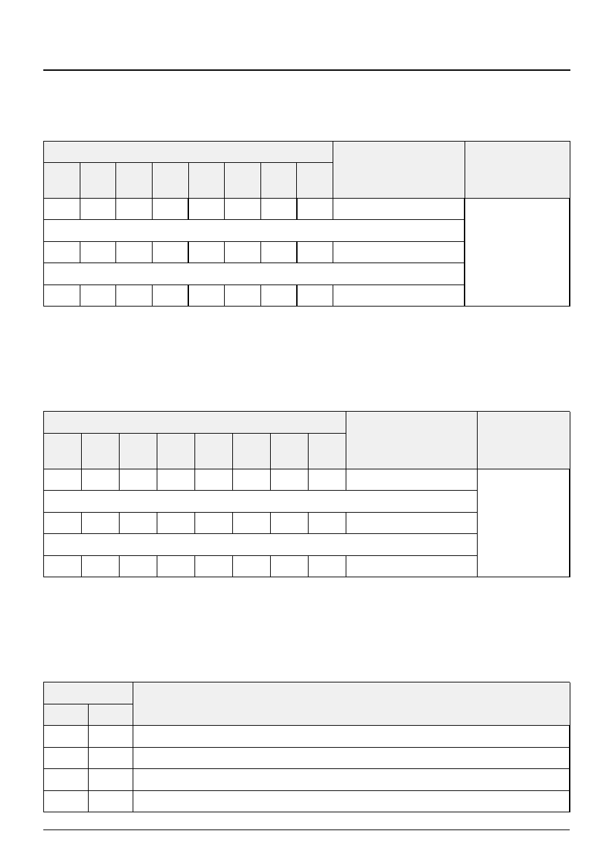
ADVANCE INFORMATION
PVP 9390A
Micronas
May 3, 2004; 6251-633-1AI
55
Subaddress 15h
Subaddress 16h
Subaddress 17h
Table 3�77: PKLG
PKLG
Peak Level Green:
Peak to peak output
voltage of the OUT2
channel
Note
D7
D6
D5
D4
D3
D2
D1
D0
0
0
0
0
0
0
0
0
0.3 V
pp
Values refer to con-
trast (CONADJ) and
brightness (BRT-
ADJ) at minimum
...
1
1
0
0
0
0
0
0
1 V
pp
...
1
1
1
1
1
1
1
1
1.2 V
pp
Table 3�78: PKLB
PKLB
Peak Level Blue:
Peak to peak output
voltage of the OUT2
channel
Note
D7
D6
D5
D4
D3
D2
D1
D0
0
0
0
0
0
0
0
0
0.3 V
pp
Values refer to
contrast (CON-
ADJ) and bright-
ness (BRTADJ)
at minimum
...
1
1
0
0
0
0
0
0
1 V
pp
...
1
1
1
1
1
1
1
1
1.2 V
pp
Table 3�79: MAT
MAT
RGB Matrix Select:
Selects the RGB matrix coefficients for YUV to RGB conversion
D7
D6
0
0
EBU- Matrix
0
1
NTSC-Japan Matrix
1
0
NTSC-USA Matrix
1
1
(Reserved)

PVP 9390A
ADVANCE INFORMATION
56
May 3, 2004; 6251-633-1AI
Micronas
Subaddress 18h
Table 3�80: BGY
BGY
Background Color Y:
Adjusts the Y background color component the values gives the two MSBs of the Y
background signal
D5-D4
Table 3�81: FRY
FRY
Frame Color Y:
Adjusts the Y frame color component the value gives the 4 MSBs of the Y frame signal
D3-D0
Table 3�82: OUTFOR
OUTFOR
Output Format:
Switches between RGB output and YUV output
D7
0
RGB output signals, matrix active
1
YUV output signals
Table 3�83: UVPOLAR
UVPOLAR
UV Polarity:
Switches between UV or inverted UV output, has no influence in RGB mode
D6
0
+U / +V output
1
-
U /
-
V output
Table 3�84: BGU
BGU
Background Color U:
Adjusts the U background color component the values gives the two MSBs of the U
background signal
D5-D4
ADVANCE INFORMATION
PVP 9390A
Micronas
May 3, 2004; 6251-633-1AI
57
Subaddress 19h
Table 3�85: FRU
FRU
Frame Color U:
Adjusts the U frame color component the value gives the 4 MSBs of the U frame signal
D3-D0
Table 3�86: BGFRC
BGFRC
Background Frame Color:
Selects background color table or frame color table for background color
D6
0
Background color according to BGY, BGU, BGV
1
Background color according to FRY, FRU, FRV
Table 3�87: BGV
BGV
Background Color V:
Adjusts the V background color component the values gives the two MSBs of the V
background signal
D5-D4
Table 3�88: FRV
FRV
Frame Color V:
Adjusts the V frame color component the value gives the 4 MSBs of the V frame signal
D3-D0
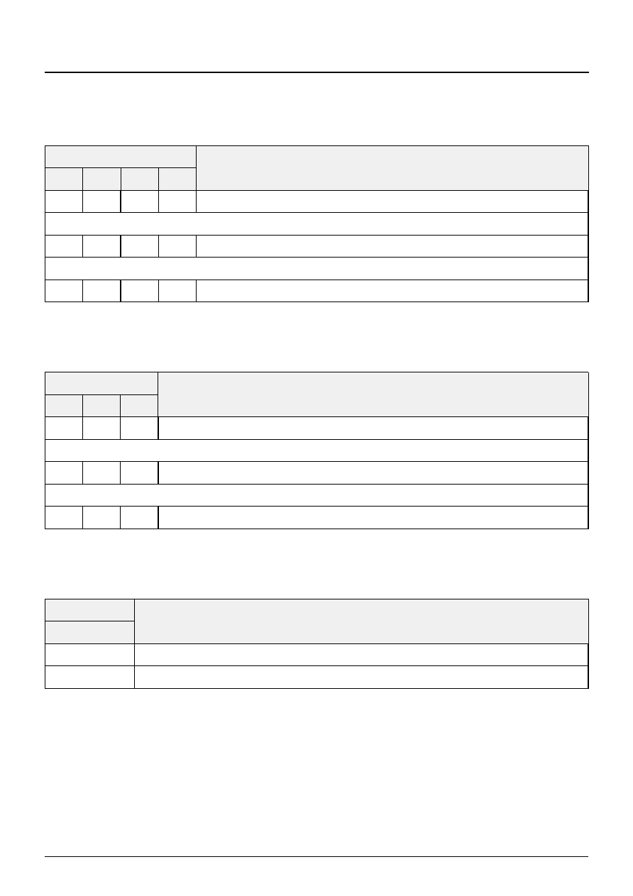
PVP 9390A
ADVANCE INFORMATION
58
May 3, 2004; 6251-633-1AI
Micronas
Subaddress 1Ah
Table 3�89: SATADJ
SATADJ
Color Saturation Adjustment:
Adjusts the color saturation in steps of x/8
D7
D6
D5
D4
0
0
0
0
No color
...
1
0
0
0
Nominal saturation
...
1
1
1
1
1.875 times saturation
Table 3�90: YPEAK
YPEAK
Y Peaking Adjustment:
Adjusts luminance peaking
D3
D2
D1
0
0
0
No peaking
...
0
1
1
Recommended value
...
1
1
1
Strongest peaking
Table 3�91: YCOR
YCOR
Y Coring Enable:
Suppresses noise introduced by peaking
D0
0
Coring off
1
1 LSB coring
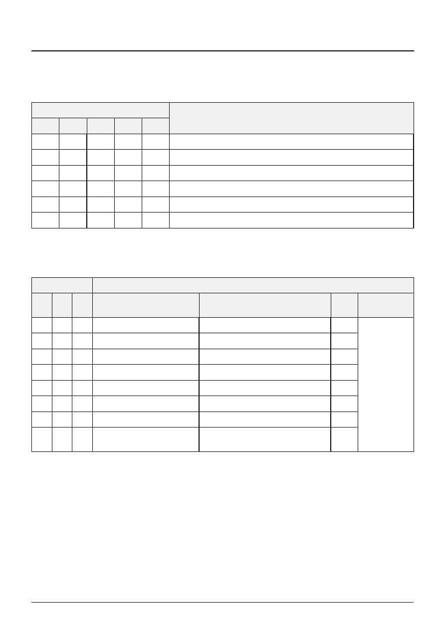
ADVANCE INFORMATION
PVP 9390A
Micronas
May 3, 2004; 6251-633-1AI
59
Subaddress 1Bh
Table 3�92: XDSCLS
XDSCLS
XDS Class Select:
Closed Caption XDS-Primary Filter (Class)
D7
D6
D5
D4
D3
0
0
0
0
0
Transparent, no filtering
1
X
X
X
X
`Current' class selected
X
1
X
X
X
`Future' class selected
X
X
1
X
X
`Channel' class selected
X
X
X
1
X
`Miscellaneous' class selected
X
X
X
X
1
`Public Services' class selected
Table 3�93: XDSTPE
XDSTPE
XDS Type Select/WSS Field Select
D2
D1
D0
XDS-Secondary Filter Type
Meaning
WSS
field
Note
0
0
0
All No
filtering
0
Behavior of
these bits
depends on
selected data-
service
0
0
1
05h
Program rating
1
0
1
0
01h, 04h
Time information only
0/1
0
1
1
40h
Out of band only
0/1
1
0
0
01h, 02h, 03h, 04h, 0Dh, 40h
VCR information
0/1
1
0
1
01h, 04h, 05h
Time information and program rating
0/1
1
1
0
05h, 40h
Out of band and program rating
0/1
1
1
1
01h, 02h, 03h, 04h, 05h, 0Dh,
40h
VCR information and program rating
0/1
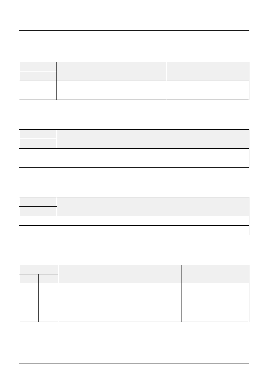
PVP 9390A
ADVANCE INFORMATION
60
May 3, 2004; 6251-633-1AI
Micronas
Subaddress 1Ch
Table 3�94: UVSEQ
UVSEQ
UV Sequence:
Changes the UV multiplex sequence
Note
D7
0
U and V are correct
Valid only if YUVSEL= `1'
1
U and V are exchanged
Table 3�95: MPIPBG
MPIPBG
Multi-PIP Background:
Selects the background color for multi-PIP mode
D6
0
Black
1
Same as background color
Table 3�96: SERVICE
SERVICE
Data Service Select:
Selects data service for slicing
D5
0
Closed Caption
1
Widescreen Signalling (WSS)
Table 3�97: SELLNR
SELLNR
Select Line Number:
Line number of data service field 0 (field1)
Note
D4
D3
0
0
[NTSC] 20 (283), [PAL M] 17 (280)
WSS
0
1
[NTSC] 21 (284), [PAL M] 18 (281)
Closed Caption
1
0
[PAL B/G] 22 (329)
Closed Caption
1
1
[PAL B/G] 23 (330)
WSS
ADVANCE INFORMATION
PVP 9390A
Micronas
May 3, 2004; 6251-633-1AI
61
Subaddress 1Dh
Table 3�98: IRQCON
IRQCON
Interrupt Request Pin Configuration:
Output of INT pin is:
Note
D2
D1
D0
0
0
0
Tri-state (high-Z)
0
0
1
Interrupt, when new data received
(neg. polarity)
Pulse length is approximately
2
�
s
0
1
0
Interrupt, when new data received
(pos. polarity)
0
1
1
Equivalent to DATAV for both registers (neg. polarity)
1
0
0
Equivalent to DATAV for both registers (pos. polarity)
1
0
1
Inset V-pulse (neg. polarity)
Pulse length is 50 ns
1
1
0
Inset field
High = first field, low = second
field,
1
1
1
Inset clamping pulse (neg. polarity)
Only for test purpuse
Table 3�99: PALIDL2
PALIDL2
PAL/NTSC identifikation level 2 :
Sensitivity of identification of PAL/NTSC signals
D5
0
1/2 or 1/4
1
1/8 or 1/16
Table 3�100: PALIDL1
PALIDL1
PAL/NTSC identifikation level 1:
Sensitivity of identification of PAL/NTSC signals
D4
D3
0
0
+0
0
1
+32
1
0
+64
1
1
+128
PVP 9390A
ADVANCE INFORMATION
62
May 3, 2004; 6251-633-1AI
Micronas
Subaddress 1Eh
Table 3�101: PIPBLK
PIPBLK
PIP Blank:
Blanks the current picture by setting it to background color
D2
0
No blank
1
Blanks the current selected (WRPOS) PIP
Table 3�102: PALIDL
PALIDL
PAL ID Level:
Sensitivity of identification of PAL/NTSC signals
D0
0
High rejection of PAL/NTSC
1
Low rejection of PAL/NTSC
Table 3�103: POSOFV
POSOFV
Position Offset Vertical:
Vertical position offset in steps of 4 lines
D7
D6
D5
1
0
0
-
16 lines
...
0
0
0
0 lines
...
0
1
1
+12 lines
ADVANCE INFORMATION
PVP 9390A
Micronas
May 3, 2004; 6251-633-1AI
63
Subaddress 1Fh
Subaddress 20h
Table 3�104: POSOFH
POSOFH
Position Offset Horizontal:
Horizontal position offset in steps of 16 pixel
D4
D3
D2
D1
D0
1
0
0
0
0
-
256 pixel
...
0
0
0
0
0
0 pixel
...
0
1
1
1
1
+240 pixel
Table 3�105: VSHRNK
VSHRNK
Vertical Shrink:
Changes the vertical size in steps of 2 lines
Note
D4
D3
D2
D1
D0
0
0
0
0
0
No shrink, picture size according to SIZEVER
Max. usable value
depends on
SIZEVER
...
1
1
1
1
1
Max. possible shrink
Table 3�106: HSHRNK
HSHRNK
Horizontal Shrink:
Changes the horzontal size in steps of 4 pixel
Note
D4
D3
D2
D1
D0
0
0
0
0
0
No shrink, picture size according to SIZEHOR
Max. usable value
depends on
SIZEVER
...
1
1
1
1
1
Max. possible shrink
PVP 9390A
ADVANCE INFORMATION
64
May 3, 2004; 6251-633-1AI
Micronas
Subaddress 21h
Subaddress 22h
Table 3�107: DWCOR
DWCOR
Test only
D3
0
(Reserved)
1
Normal operation
Table 3�108: PKBOOST
PKBOOST
Peaking Boost:
Influences peaking of YPEAK (A2h)
D2
0
Use normal peaking values
1
Double peaking values
Table 3�109: CLPLEN
CLPLEN
Clamping Pulse Length
D1
D0
Clamping Pulse Length
Blanking Duration
Note
0
0
5
�
s
10.5
�
s
The clamping pulse length and the
blanking is also influenced by the
setting of READD and HZOOM
0
1
3.75
�
s
7.9
�
s
1
0
2.5
�
s
5.2
�
s
1
1
1.25
�
s
2.6
�
s
Table 3�110: PIPHLT
PIPHLT
PIP Highlighting:
Highlights the current selected (WRPOS) PIPr
D7
0
No highlighting
1
Highlighting the PIP
ADVANCE INFORMATION
PVP 9390A
Micronas
May 3, 2004; 6251-633-1AI
65
Subaddress 23h
Table 3�111: ABRTHD
ABRTHD
Automatic Brightness Reduction Threshold:
Threshold adjustment for reduction of luminance magnitude
D6
D5
D4
D3
0
0
0
0
ABR off
0
0
0
1
ABR threshold at luminance value of 240
...
1
1
1
1
ABR threshold at luminance value of 180
Table 3�112: ABRSPD
ABRSPD
Automatic Brightness Reduction Speed:
Speed adjustment for reduction of luminance magnitude
D2
D1
D0
0
0
0
2 fields
...
1
1
1
16 fields
Table 3�113: INFRMOD
INFRMOD
Inner Frame Modification:
Modifies the look of the frame for dual-PIP applications
D7
0
Inner frame suited for usage of single PIP applications
1
Inner frame suited for usage of dual PIP applications
Table 3�114: DISPMOD
DISPMOD
Display Mode:
Selects the single PIP modes, multi-PIP modes or
double-window mode
Note
D6
D5
D4
D3
D2
0
0
0
0
0
Single PIP mode
See Table 2�9 on
page 15 for
description of
modes
...
1
0
0
1
0
OSD only mode
PVP 9390A
ADVANCE INFORMATION
66
May 3, 2004; 6251-633-1AI
Micronas
Subaddress 24h
Table 3�115: WIPESP
WIPESP
Wipe Speed:
Selects the period for opening/closing the PIP window
D1
D0
0
0
Wipe off
0
1
1/3 second
1
0
2/3 second
1
1
1 second
Table 3�116: CZMEN
CZMEN
Continuos Zoom Enable:
Controls the update of the picture size
D7
0
Delayed execution of HDEC/VDEC/HSHRNK/VSHRNK update
1
Picture size will be updated
Table 3�117: CZMSP
CZMSP
Continuos Zoom Speed:
Speed setting for continous zooming
Note
D6
D5
0
0
No zoom
1 step means 20 pixel and 8 lines (PAL) or
6 lines (NTSC) decrement or increment
0
1
1 step per 1 fields
1
0
1 step per 2 fields
1
1
1 step per 4 fields
ADVANCE INFORMATION
PVP 9390A
Micronas
May 3, 2004; 6251-633-1AI
67
Subaddress 25h
Table 3�118: WRPOS
WRPOS
Write Position:
Position of the current written picture
Note
D3
D2
D1
D0
0
0
0
0
First writing position = first picture
Number of last valid writing posi-
tion depends on display mode
(DISPMOD)
0
0
0
1
Second writing position
...
1
0
0
1
Maximum writing position
Table 3�119: CHRFRC
CHRFRC
Character Frame Color:
Modifies the character color
D7
0
Character luminance table used
1
Frame color table used
Table 3�120: CHRDHW
CHRDHW
Character Double Height and Width:
Doubles the characters' height and width
D6
0
Normal height and width
1
Double height and width
Table 3�121: CHRY
CHRY
Character Luminance:
Character luminance level (IRE)
Note
D5
D4
0
0
60
Valid only if CHRFRC = `0', charac-
ter chrominance is 0 IRE
0
1
70
1
0
80
1
1
90

PVP 9390A
ADVANCE INFORMATION
68
May 3, 2004; 6251-633-1AI
Micronas
Subaddress 26h
Table 3�122: CHRBGY
CHRBGY
Character Background Luminance:
Character background luminance level (IRE)
D3
D2
0
0
10
0
1
20
1
0
30
1
1
40
Table 3�123: CHRBGON
CHRBGON
Character Background On:
Defines the characters' background
Note
D1
D0
0
0
No character background (transparent mode)
0
1
Character background (dependent on CHRBGY)
1
0
Semi-transparent mode (black&white)
Not possible in case of active back-
ground in PIP
1
1
Semi-transparent mode (colored)
Table 3�124: OSDON
OSDON
OSD On:
Switches OSD on
D7
0
OSD off
1
OSD on
ADVANCE INFORMATION
PVP 9390A
Micronas
May 3, 2004; 6251-633-1AI
69
Subaddress 27h
Table 3�125: CHRADR
CHRADR
Character Address
D6
D5
D4
D3
D2
D1
D0
No. Picture
No. Character
Note
0
0
0
0
0
0
0
0
0
Will be auto-
incremented
with every write
access to CHR-
COD
0
0
0
0
0
0
1
0
1
...
0
0
0
0
1
0
0
0
4
0
0
0
1
0
0
1
1
1
...
1
0
1
1
1
0
0
11
4
Table 3�126: CHRCLR
CHRCLR
Character Clear:
Resets all characters to `blank' character
D7
0
No blank
1
Character reset
Table 3�127: CHRCOD
CHRCOD
Character Code:
Character code, see Appendix
D6-D0
PVP 9390A
ADVANCE INFORMATION
70
May 3, 2004; 6251-633-1AI
Micronas
Subaddress 28h
Table 3�128: FRMMD
FRMMD
Frame Mode Indication:
PIP displays field or frame mode
D7
0
Field mode, one field is repeated twice
1
Frame mode, both fields are displayed
Table 3�129: PIPSTAT
PIPSTAT
PIP Status:
Indication of visibility of PIP, corresponds to PIPON
D6
0
PIP off
1
PIP on
Table 3�130: SYSNCST
SYNCST
Inset Synchronization Status:
Inset synchronization PLL is
D5
D4
0
0
Not locked to CVBS signal
0
1
1
0
Locked to CVBS signal (60 Hz)
1
1
Locked to CVBS signal (50 Hz)
Table 3�131: CKSTAT
CKSTAT
Color Killer Status:
Chroma is
D3
0
Off
1
On
ADVANCE INFORMATION
PVP 9390A
Micronas
May 3, 2004; 6251-633-1AI
71
Subaddress 2Ah
Subaddress 2Bh
Table 3�132: STDET
STDET
Standard Detection:
Detected color standard
D2
D1
D0
0
0
0
Non-standard or standard not detected
0
0
1
NTSC-M
0
1
0
PAL-M
0
1
1
NTSC44
1
0
0
PAL60
1
0
1
PAL-N
1
1
0
SECAM
1
1
1
PAL-B/G
Table 3�133: DATAA
DATAA
First Data Byte:
First word of sliced data, D7 = MSB, D0 = LSB
D7-D0
Table 3�134: DATAB
DATAB
Second Data Byte:
Second word of sliced data, D7 = MSB, D0 = LSB
D7-D0

PVP 9390A
ADVANCE INFORMATION
72
May 3, 2004; 6251-633-1AI
Micronas
Subaddress 2Ch
Table 3�135: PALDET
PALDET
PAL identification:
PAL identification (algorithm B)
D7
0
Not PAL
1
PAL
Table 3�136: DEVICE
DEVICE
Device Identification:
Micronas PIP IC
D5
D4
0
0
SDA 9488X (PIP IV Basic)
0
1
SDA 9489X (PIP IV Advanced)
1
0
SDA 9588X (OCTOPUS)
1
1
SDA 9589X (SOPHISTICUS) / PVP 9390A (see Table 3�202 on page 89).
Table 3�137: PRNSTD
PRNSTD
Parent Standard Detection:
Status of parent (display) standard detection
D3
0
60 Hz field frequency detected
1
50 Hz field frequency detected
Table 3�138: PALID
PALID
PAL Identification:
Identification of PAL signal (algorithm A)
Note
D2
0
NTSC signal
Not valid if STDET= `000'
1
PAL signal
ADVANCE INFORMATION
PVP 9390A
Micronas
May 3, 2004; 6251-633-1AI
73
Subaddress 2Eh
Table 3�139: DATAV
DATAV
Data Valid:
New data indication, used for data flow control (polling mode)
D1
0
Data read via I
2
C or no data available
1
New data received and available in DATAA and DATAB
Table 3�140: SLFIELD
SLFIELD
Sliced Data Field Number:
DATAA and DATAB are from
D0
0
First field
1
Second field
Table 3�141: SCMREL
SCMREL
Secam Rejection Level
D7
D6
0
0
320
0
1
384
1
0
352
1
1
1024
Table 3�142: SCMIDL
SCMIDL
SECAM Identifikation Level
D5
D4
D3
0
0
0
128
0
0
1
64
0
1
0
96
0
1
1
80
PVP 9390A
ADVANCE INFORMATION
74
May 3, 2004; 6251-633-1AI
Micronas
Subaddress 2Fh
1
0
0
70
1
0
1
76
1
1
0
84
1
1
1
90
Table 3�142: SCMIDL, continued
SCMIDL
SECAM Identifikation Level
D5
D4
D3
Table 3�143: SCCDIV
SCCDIV
Secam Divider
D2
0
Divide by 4
1
Divide by 2
Table 3�144: BELLIIR
BELLIIR
Bellfilter Adjustment
D0
0
17/64
1
12/64
Table 3�145: PALINC1
PALINC1
PAL increment 1:
PAL/NTSC identification
D7
0
+3
1
+2

ADVANCE INFORMATION
PVP 9390A
Micronas
May 3, 2004; 6251-633-1AI
75
Table 3�146: PALINC2
PALINC2
PAL increment 2:
PAL/NTSC identification
D6
0
-
1
1
-
2
Table 3�147: LOCKSP
LOCKSP
Locking Speed:
Duration of chroma PLL search
D5
D4
0
0
25 fields
0
1
20 fields
1
0
17 fields
1
1
15 fields
Table 3�148: SECACCL
SECACCL
Secam Acceptance Level
D3
D2
D1
0
0
0
100
0
0
1
84
0
1
0
64
0
1
1
32
1
0
0
70
1
0
1
76
1
1
0
90
1
1
1
(Reserved)
PVP 9390A
ADVANCE INFORMATION
76
May 3, 2004; 6251-633-1AI
Micronas
Subaddress 30h
Table 3�149: SECACC
SECACC
Secam Acceptance
D0
0
Disabled
1
Enabled
Table 3�150: ADLCK
ADLCK
Additional Lock-detection
D7
0
Do not use lock signal
1
Use lock-signal
Table 3�151: ADLCKSEL
ADLCKSEL
Additional Lock-detection Selection
D6
0
PALID
1
PALDET
Table 3�152: ADLCKCC
ADLCKCC
Additional Lock-detection Color-killer
D5
0
Do not use lock signal
1
Use lock-signal
ADVANCE INFORMATION
PVP 9390A
Micronas
May 3, 2004; 6251-633-1AI
77
Subaddress 31h
Table 3�153: CLRANGE
CLRANGE
Chroma Lock-range
D4
D3
0
0
�
425 Hz
0
1
�
463 Hz
1
0
�
505 Hz
1
1
�
550 Hz
Table 3�154: NADJ
NADJ
Notch Adjustment:
Color-carrier notch adjustment
D2
D1
D0
0
0
0
Broadest notch
...
1
1
1
Steepest notch
Table 3�155: NSRED
NSRED
Noise Reduction for Horizontal PLL
D7
D6
D5
0
0
0
1/16
0
0
1
1/8
0
1
0
1/4
0
1
1
1/2
1
0
0
1
1
0
1
2
1
1
0
4
1
1
1
8
PVP 9390A
ADVANCE INFORMATION
78
May 3, 2004; 6251-633-1AI
Micronas
Subaddress 32h
Table 3�156: SLLTHD
SLLTHD
Slicing Level Threshold H
D4
D3
0
0
No offset
0
1
Adaptive negative (limited to
�
4)
1
0
Adaptive positive (limited to
�
4)
1
1
Adaptive positive (limited to
�
8)
Table 3�157: ISHFT
ISHFT
I-Adjustment for Horizontal PLL
D2
D1
0
0
*1
0
1
*2
1
0
*4
1
1
*8
Table 3�158: ENLIM
ENLIM
Enable Limiter
D0
0
Disabled
1
Enabled
Table 3�159: DETECT5060
DETECT5060
Detection of 50 and 60 Hz Signals
D7
0
Immediately
1
Delayed
ADVANCE INFORMATION
PVP 9390A
Micronas
May 3, 2004; 6251-633-1AI
79
Subaddress 33h
Subaddress 34h
Table 3�160: VTHRL50
VTHRL50
Vertical Window Noise Suppression Opening
50 Hz
Note
D6-D0
0000000
Opening in first line
Opening=4*VTHRL50
...
1111111
Opening in line 508
Table 3�161: BCOROFF
BCOROFF
Blanklevel Coring Off:
Blanklevel generation coring (for sync-tip clamping only)
D7
0
Coring on
1
Coring off
Table 3�162: VTHRL60
VTHRL60
Vertical Window Noise Suppression Opening
60 Hz
Note
D6-D0
0000000
Opening in first line
Opening=4*VTHRL60
...
1111111
Opening in line 508
Table 3�163: VTHRH60
VTHRH60
Vertical Window Noise Suppression Closing
60 Hz
Note
D3-D0
0000
Closing in line 262
Closing=262+4*VTHRH60
...
1111
Closing in line 262+60
PVP 9390A
ADVANCE INFORMATION
80
May 3, 2004; 6251-633-1AI
Micronas
Subaddress 35h
Table 3�164: VTHRH50
VTHRH50
Vertical Window Noise Suppression Closing
50 Hz
Note
D7-D4
0000
Closing in line 312
Closing=312+4*VTHRH50
...
1111
Closing in line 312+60
Table 3�165: CLMPSTGY
CLMPSTGY
Clamping Strategy
D7
0
Back-porch clamping
1
Sync-tip-clamping
Table 3�166: SLLTHDVP
SLLTHDVP
Slicing Level Threshold V Polarity
D6
0
Positive
1
Negative
ADVANCE INFORMATION
PVP 9390A
Micronas
May 3, 2004; 6251-633-1AI
81
Table 3�167: SLLTHDV
SLLTHDV
Slicing Level Threshold V
D5
D4
D3
0
0
0
No offset
0
0
1
4
0
1
0
8
0
1
1
12
1
0
0
(Reserved)
1
0
1
Adaptive (limited to
�
4)
1
1
0
Adaptive (limited to
�
8)
1
1
1
Adaptive (limited to
�
12)
Table 3�168: VFLYWHLMD
VFLYWHLMD
Vertical Flywheel Mode
D2
D1
0
0
Check for correct standard
0
1
3 lines deviation allowed
1
0
4 lines deviation allowed, no check for interlace
1
1
5 lines deviation allowed, no check for interlace
Table 3�169: VFLYWHL
VFLYWHL
Vertical Flywheel
D0
0
Disabled
1
Enabled

PVP 9390A
ADVANCE INFORMATION
82
May 3, 2004; 6251-633-1AI
Micronas
Subaddress 36h
Table 3�170: FLNSTRD
FLNSTRD
Force Line Standard at CVBS/RGB Front-end
D7
D6
0
0
Automatic
0
1
Force 50 Hz
1
0
Force 60 Hz
1
1
(Reserved)
Table 3�171: CLMPCHARY
CLMPCHARY
Clamping Characteristic Y/CVBS:
Characteristic of clamping error vs. clamping current
D5
D4
0
0
High gain
0
1
Medium gain 1
1
0
Medium gain 2
1
1
Low gain
Table 3�172: VDETIFS
VDETIFS
Vertical Detection Slope
D3
0
Normal
1
Slow
Table 3�173: VDETITC
VDETITC
Vertical Detection Integration Time Constant
D2
0
Long
1
Short
ADVANCE INFORMATION
PVP 9390A
Micronas
May 3, 2004; 6251-633-1AI
83
Subaddress 37h
Table 3�174: VLP
VLP
Lowpass for Vertical Sync-separation
D1
D0
0
0
None
0
1
Weak
1
0
Medium
1
1
Strong
Table 3�175: LATENCY
LATENCY
Clamping Latency:
... additional idle-states
D7
D6
0
0
0
0
1
2
1
0
4
1
1
6
Table 3�176: FILTBRST
FILTBRST
Burst filter for Y/CVBS ADC
D5
0
Disabled
1
Enabled
Table 3�177: CLMPIST
CLMPIST
Start of Clamping Pulse
Note
D4-D0
00000
0.5
�
s
START=0.5
�
s+CLMPIST*0.25
�
s
...
11111
8.25
�
s
PVP 9390A
ADVANCE INFORMATION
84
May 3, 2004; 6251-633-1AI
Micronas
Subaddress 38h
Table 3�178: CLKP_INV
CLKP_INV
Parent Clock Inversion:
Controls the inversion of the parent clock
D3
0
Not inverted
1
Inverted
Table 3�179: INCRSEL
INCRSEL
Increment Select
D3
0
Select display clock according to HZOOM
1
Adjust display clock with DTOINCR
Table 3�180: FINECLMP
FINECLMP
Fine clamping enable
D2
0
Use default clamping for ADC
1
Use fine clamping for ADC
Table 3�181: INSEL
INSEL
Input select
D1
D0
0
0
Select input by CVBSEL, YUVSEL
0
1
CVBS4
1
0
Y (CVBS1), C (CVBS2)
1
1
YUV

ADVANCE INFORMATION
PVP 9390A
Micronas
May 3, 2004; 6251-633-1AI
85
Subaddress 39h
Subaddress 3Ah
Table 3�182: DTOINCR
DTOINCR
DTO increment
D7-D0
0000000
20.25 MHz
...
1111111
40.42 MHz
Table 3�183: GPO
GPO
GPO0-2 Pin Output Level
D4-D2
001
GPO0 = 1, GPO1 = 0, GPO2 = 0
Table 3�184: GPOEN
GPOEN
GPO Pin Enable
D1
0
GPO0-2 = `Z'
1
See GPO
Table 3�185: CLKOUTEN
CLKOUTEN
Enable Clock Output CLKOUT
D0
0
Disabled
1
Enabled
PVP 9390A
ADVANCE INFORMATION
86
May 3, 2004; 6251-633-1AI
Micronas
Subaddress 3Bh
Subaddress 3Ch
Table 3�186: YSYNCOFS
YSYNCOFS
Sync Offset Enable
D0
0
Disabled, Y or G without sync at IN2
1
Enabled, Y or G with sync at IN2
Table 3�187: AFIL_OFF
AFILOFF
Anti-alias Filter Off
D5
0
Anti-alias filter for ADCs enabled
1
Anti-alias filter for ADCs disabled
Table 3�188: STBY_REF
STBY_REF
Standby ADC Reference
D4
0
Reference active
1
Standby
Table 3�189: STBY_OTA
STBY_OTA
Standby OTA
D3
0
OTA active
1
Standby
ADVANCE INFORMATION
PVP 9390A
Micronas
May 3, 2004; 6251-633-1AI
87
Subaddress 3Dh
Table 3�190: STBY_ADC1
STBY_ADC1
Standby ADC1
D2
0
ADC1 active
1
Standby
Table 3�191: STBY_ADC2
STBY_ADC2
Standby ADC2
D1
0
ADC2 active
1
Standby
Table 3�192: STBY_ADC3
STBY_ADC3
Standby ADC3
D0
0
ADC3 active
1
Standby
Table 3�193: STBY_BUFFER
STBY_BUFFER
Standby Buffer
D7
0
Buffer active
1
Standby
PVP 9390A
ADVANCE INFORMATION
88
May 3, 2004; 6251-633-1AI
Micronas
Table 3�194: STBY_CLAMP
STBY_CLAMP
Standby Clamping
D6
0
Clamping active
1
Standby
Table 3�195: STBY_DAC1
STBY_DAC1
Standby DAC1
D5
0
DAC1 active
1
Standby
Table 3�196: STBY_DAC2
STBY_DAC2
Standby DAC2
D4
0
DAC2 active
1
Standby
Table 3�197: STBY_DAC3
STBY_DAC3
Standby DAC3
D3
0
DAC3 active
1
Standby
Table 3�198: STBY_GAIN
STBY_GAIN
Standby Gain DAC
D2
0
Gain DAC active
1
Standby

ADVANCE INFORMATION
PVP 9390A
Micronas
May 3, 2004; 6251-633-1AI
89
Subaddress 3Eh
Subaddress 3Fh
Table 3�199: STBY_OFFSET
STBY_OFFSET
Standby Offset DAC
D1
0
Offset DAC active
1
Standby
Table 3�200: STBY_REF
STBY_REF
Standby DAC reference
D0
0
Reference active
1
Standby
Table 3�201: TRIM_BGP
TRIM_BGP
Trim Bandgap
D7-D0
Table 3�202: PVPREV
PVPREV
PVPA Revision
D1
D0
0
0
Old devices
0
1
PVPA 9390
1
0
Reserved for future use
1
1
Reserved for future use
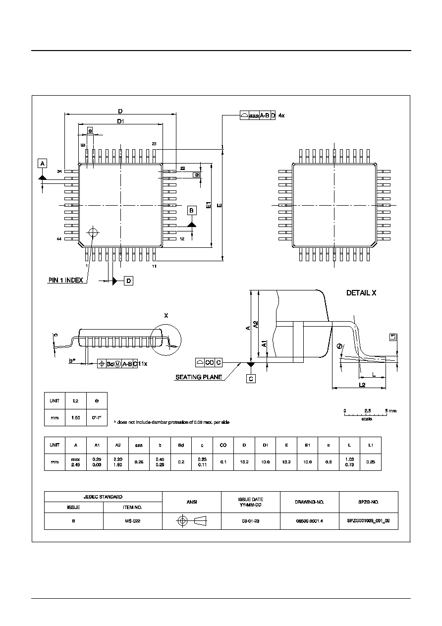
PVP 9390A
ADVANCE INFORMATION
90
May 3, 2004; 6251-633-1AI
Micronas
4. Specifications
4.1. Outline Dimensions
Fig. 4�1:
PMQFP44-1: Plastic Metric Quad Flat Package, 44 leads, 10
�
10
�
2 mm
3
Ordering code: QG
Weight approximately 0.5 g

ADVANCE INFORMATION
PVP 9390A
Micronas
May 3, 2004; 6251-633-1AI
91
4.2. Pin Connections and Short Descriptions
NC = not connected, leave vacant
LV = if not used, leave vacant
STG = short to GND
OBL = obligatory; connect as described in circuit diagram
Pin
No.
Pin Name
Type
Connection
(If not used)
Short Description
1
XOUT
O
OBL
Crystal oscillator (output)
2
XIN
I
OBL
Crystal oscillator (input) or external clock input
3
VSS18
Supply
OBL
1.8 V digital core ground
4
VDD18
Supply
OBL
1.8 V digital core supply
5
GPO0
I/O
LV
General purpose output
6
SEL
O
OBL
Fast blanking output for PIP
7
OUT3
O/Analog
OBL
Analogue output: chrominance signal +(B-Y) or -(B-
Y) or B
8
OUT2
O/Analog
OBL
Analogue output: luminance signal Y or G
9
OUT1
O/Analog
OBL
Analogue output: chrominance signal +(R-Y) or
-(R-Y) or R
10
VSS33DAC
Supply
OBL
3.3 V DAC analog ground
11
VDD33DAC
Supply
OBL
3.3 V DAC analog supply
12
FSW
I
LV
Fast switch input for YUV/RGB switch
13
IN3
I/Analog
LV
U/B input for external YUV/RGB source
14
IN2
I/Analog
LV
Y/G input for external YUV/RGB source
15
IN1
I/Analog
LV
V/R input for external YUV/RGB source
16
VDD18ADC
Supply
OBL
1.8 V ADC analog supply
17
VSS18ADC
Supply
OBL
1.8 V ADC analog ground
18
CVBS1
I/Analog
LV
CVBS1 or Y (from YUV) input
19
TEST
I/O
STG
Reserved (tie to VSS)
20
CVBS2
I/Analog
LV
CVBS2 or U or Y (from Y/C) input
21
TM
I
STG
Test mode (tie to VSS)
22
CVBS3
I/Analog
LV
CVBS3 or V or C Input
23
CVBS4
I/Analog
LV
CVBS4
24
VSS33ADC
Supply
OBL
3.3 V ADC analog ground
25
VDD33ADC
Supply
OBL
3.3 V ADC analog supply
26
YIN
I/Analog
LV
Y input
27
UIN
I/Analog
LV
U input

PVP 9390A
ADVANCE INFORMATION
92
May 3, 2004; 6251-633-1AI
Micronas
28
VIN
I/Analog
LV
V input
29
RESET
I
OBL
Asynchronous reset input
30
VDD18
Supply
OBL
1.8 V digital core supply
31
VSS18
Supply
OBL
1.8 V digital core ground
32
POR
O
LV
Reserved (open)
33
GPO2
I/O
LV
General purpose output
34
I2C1
I
OBL
I�C
Address 1
35
I2C2
I
OBL
I�C
Address 2
36
SDA
I/O
OBL
I�C
-bus data
37
SCL
I
OBL
I�C
-bus clock
38
INTR
O
LV
Interrupt output
39
VDD33PAD
Supply
OBL
3.3 V digital pad supply
40
VSS33PAD
Supply
OBL
3.3 V digital pad ground
41
VSP
I
OBL
Vertical sync for parent channel
42
HSP
I
OBL
Horizontal sync for parent channel
43
GPO1
I/O
LV
General purpose output
44
CLKOUT
O
LV
Clock output
Pin
No.
Pin Name
Type
Connection
(If not used)
Short Description

ADVANCE INFORMATION
PVP 9390A
Micronas
May 3, 2004; 6251-633-1AI
93
4.3. Pin Configurations
Fig. 4�2: PMQFP44-1 Package
34
35
36
37
38
39
40
41
42
43
44
22
21
20
19
18
17
16
15
14
13
12
1
2
3
4
5
6
7
8
9
10 11
33 32 31 30 29 28 27 26 25 24 23
I2C1
I2C2
SDA
SCL
INTR
VDD33PAD
VSS33PAD
VSP
HSP
GPO1
CLKOUT
CVBS3
TM
CVBS2
TEST
CVBS1
VSS18ADC
VDD18ADC
IN1
IN2
IN3
FSW
POR
VSS18
VDD18
RESET
VIN
GPO2
UIN
YIN
VDD33ADC
VSS33ADC
CVBS4
XIN
VSS18
VDD18
GPO0
SEL
XOUT
OUT3
OUT2
OUT1
VSS33DAC
VDD33DAC
PVP 9390A

PVP 9390A
ADVANCE INFORMATION
94
May 3, 2004; 6251-633-1AI
Micronas
4.4. Electrical Characteristics
Abbreviations:
tbd = to be defined
vacant = not applicable
positive current values mean current flowing into the chip
4.4.1. Absolute Maximum Ratings
Stresses beyond those listed in the "Absolute Maximum Ratings" may cause permanent damage to the device. This
is a stress rating only. Functional operation of the device at these conditions is not implied. Exposure to absolute
maximum rating conditions for extended periods will affect device reliability.
This device contains circuitry to protect the inputs and outputs against damage due to high static voltages or electric
fields; however, it is advised that normal precautions be taken to avoid application of any voltage higher than abso-
lute maximum-rated voltages to this high-impedance circuit.
All voltages listed are referenced to ground (VSS18, VSS33PAD, VSS33DAC, VSS18ADC, VSS33ADC) except
where noted.
All GND pins must be connected to a low-resistive ground plane close to the IC.
Table 4�1: Absolute Maximum Ratings
Symbol
Parameter
Pin Name
Limit Values
Unit
Min.
Max.
T
A
1)
Ambient Operating Temperature
PMQFP44-1
-
10
70
2)
�
C
T
C
Case Operating Temperature
PMQFP44-1
-10
115
�C
T
S
Storage Temperature
-
40
125
�
C
P
max
Maximum Power Dissipation
Package PMQFP44-1
750
mW
V
SUP1
Supply Voltage 1
VDD33DAC,
VDD33ADC,
VDD33PAD
-
0.3
3.63
V
V
SUP2
Supply Voltage 2
VDD18,
VDD18ADC
-
0.3
1.98
V
V
SUP
Voltage Differences within Sup-
ply Domains
-
0.25
0.25
V
V
I
Input Voltage
All except power
supply
-
0.3
V
SUP1
+0.3 V
V
V
o
Output Voltage
All except power
supply
-
0.3
V
SUP1
+0.3 V
V
1)
Measured on Micronas typical 2-layer (1s1p) board based on JESD - 51.2 Standard with maximum power con-
sumption allowed for this package.
2)
A power-optimized board layout is recommended. The Case Operating Temperature mentioned in the Absolute
Maximum Ratings must not be exceeded at worst case conditions of the application
ADVANCE INFORMATION
PVP 9390A
Micronas
May 3, 2004; 6251-633-1AI
95
4.4.2. Recommended Operating Conditions
Functional operation of the device beyond those indicated in the "Recommended Operating Conditions/Characteris-
tics" is not implied and may result in unpredictable behavior, reduce reliability and lifetime of the device.
All voltages listed are referenced to ground (VSS18, VSS33PAD, VSS33DAC, VSS18ADC, VSS33ADC) except
where noted.
All GND pins must be connected to a low-resistive ground plane close to the IC.
Do not insert the device into a live socket. Instead, apply power by switching on the external power supply.
Symbol
Parameter
Pin Name
Limit Values
Unit
Min.
Typ.
Max.
T
A
Ambient Operating Temperature
Package PMQFP44-1
0
25
70
1)
�
C
T
C
Case Operating Temperature
Package PMQFP44-1
5
2)
45
3)
95
4)
�
C
P
max
Maximum Power Dissipation
Package PMQFP44-1
400
mW
V
SUP1
Supply Voltage 1
VDD33DAC,
VDD33ADC,
VDD33PAD
3.13
3.3
3.46
V
V
SUP2
Supply Voltage 2
VDD18,
VDD18ADC
1.71
1.8
1.89
V
V
SUP
Voltage Differences within Supply
Domains
-
0.25
0.25
V
V
IL
Input Voltage Low
0.8
V
V
IH
Input Voltage High
2.0
V
1)
A power-optimized board layout is recommended. The Case Operating Temperatures mentioned in the "Rec-
ommended Operating Conditions" must not be exceeded at worst case conditions of the application.
2)
By T
Amin
and 300 mW
3)
By T
A
=25�C and 350 mW
4)
By T
Amax
and 400 mW
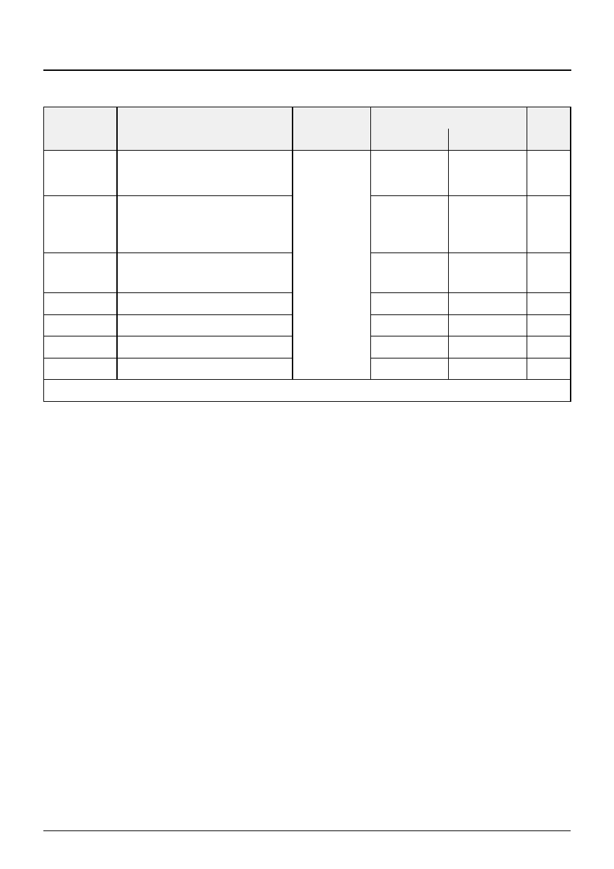
PVP 9390A
ADVANCE INFORMATION
96
May 3, 2004; 6251-633-1AI
Micronas
4.4.3. Recommended Crystal Characteristics
Symbol
Parameter
Pin Name
Limit Values
Unit
Min.
Max.
f
xtal
Frequency
(Deviation outside this range will
cause color decoding failures)
XIN, XOUT
20.248
20.25
20.252
f
max
/f
xtal
Maximum Permissible Frequency
Deviation
(Deviation outside this range will
cause color decoding failures)
-
100
100
f/f
xtal
Recommended Permissible Fre-
quency Deviation
-
40
0
40
C
L
Load Capacitance
12
27
39
R
S
Series Resonance Resistance
25
C
1
Motional Capacitance
27
C
0
Parallel Capacitance
7
In the operating range the function given in the circuit description are fulfilled.
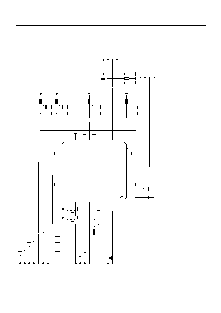
ADVANCE INFORMATION
PVP 9390A
Micronas
May 3, 2004; 6251-633-1AI
97
5. Application
5.1. Application Circuit
Fig. 5�1: Application Circuit
HP
VP
R9
100
R8
100
SCL
SD
A
C4
47n
C5
47n
C6
47n
U
Y
CVBS4
I2C
Address
J1
+3.3V
V
R5
75
R4
75
R6
75
*) depends on cr
ystal specification
XOUT
12345
6
7891
0
1
1
XIN
VSS18
VDD18
GPO0
SEL
OUT3
OUT2
OUT1
VSS33DA
C
VDD33DA
C
CVBS4
VSS33ADC
VDD33ADC
YIN
UIN
VIN
RESET
VDD18
VSS18
POR
GPO2
PVP 9390A
12
13
14
15
16
17
18
19
20
21
22
44
43
42
41
40
39
38
37
36
35
34
33
32
31
30
29
28
27
26
25
24
23
FSW
CVBS3
I2C1
CLK
OUT
IN3
IN2
IN1
VDD18ADC
VSS18ADC
CVBS1
TEST
CVBS2
TM
I2C2
SD
A
SCL
INTR
VDD33P
AD
VSS33P
AD
VSP
HSP
GPO1
X1
20.25 MHz
C24 *
18p
C23 *
18p
J2
+3.3V
C1
47n
C2
47n
C3
47n
CVBS2
CVBS1
CVBS3
R2
75
R1
75
R3
75
C16
47n
C17
47n
C18
47n
BIN
GIN
RIN
FSW
BOUT
GOUT
R
OUT
SEL
INT
RESET
C15
10n
C14
10
+3.3V
L4
10
C19
10n
C20
10
+3.3V
L5
10
C9
47n
R7
75
R11
75
R10
75
R12
75
C12
10n
C13
10
+1.8V
L3
10
C10
10n
C11
10
+3.3V
L2
10
C7
10n
C8
10
+1.8V
L1
10

All information and data contained in this data sheet are without any
commitment, are not to be considered as an offer for conclusion of a
contract, nor shall they be construed as to create any liability. Any new
issue of this data sheet invalidates previous issues. Product availability
and delivery are exclusively subject to our respective order confirmation
form; the same applies to orders based on development samples deliv-
ered. By this publication, Micronas GmbH does not assume responsibil-
ity for patent infringements or other rights of third parties which may
result from its use.
Further, Micronas GmbH reserves the right to revise this publication
and to make changes to its content, at any time, without obligation to
notify any person or entity of such revisions or changes.
No part of this publication may be reproduced, photocopied, stored on a
retrieval system, or transmitted without the express written consent of
Micronas GmbH.
PVP 9390A
ADVANCE INFORMATION
98
May 3, 2004; 6251-633-1AI
Micronas
Micronas GmbH
Hans-Bunte-Strasse 19
D-79108 Freiburg (Germany)
P.O. Box 840
D-79008 Freiburg (Germany)
Tel. +49-761-517-0
Fax +49-761-517-2174
E-mail: docservice@micronas.com
Internet: www.micronas.com
Printed in Germany
Order No. 6251-633-1AI
6. Data Sheet History
1. Advance Information: "PVP 9390A Picture-in-Pic-
ture IC", May 3, 2004, 6251-633-1AI. First release of
the advance information.