 | –≠–ª–µ–∫—Ç—Ä–æ–Ω–Ω—ã–π –∫–æ–º–ø–æ–Ω–µ–Ω—Ç: R485JMAA | –°–∫–∞—á–∞—Ç—å:  PDF PDF  ZIP ZIP |
Advance Data Sheet, Rev. 1
October 2001
R485-Type Lightwave Receiver with Clock
Recovery for 2.488 Gbits/s Applications
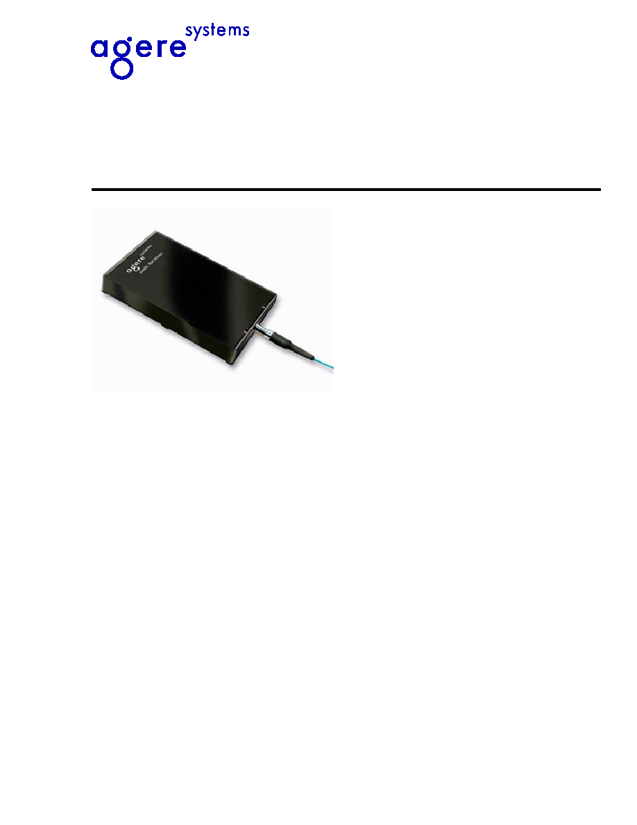
Manufactured in a low-profile, 24-pin package, the R485-Type
Receiver features either an avalanche or PIN photodetector, a
transimpedance amplifier, a limiting amplifier, and a clock and
data recovery IC.
Features
s
Multisourced footprint
s
Internal APD bias supply
s
Differential data and clock outputs
s
APD and PIN versions
s
Typical sensitivity:
--APD, ≠32 dBm
--PIN, ≠23 dBm
s
Operation at 1.3
µ
m or 1.55
µ
m
s
TTL link status flag
s
Wide operating case temperature range:
--APD, 0
∞
C to +70
∞
C
--PIN, ≠40
∞
C to +85
∞
C
s
Space-saving, self-contained, 24-pin DIP
s
Agere Systems Inc. Reliability and Qualification
Program for built-in quality
s
SONET/SDH compatible for OC-48/STM-16 data
rate
Applications
s
Telecommunications
-- Inter- and intraoffice SONET/SDH
-- Subscriber loop
-- Metropolitan area networks
s
High-speed data communications
Description
The R485-Type 2.5 Gbits/s lightwave receiver is
designed for use in SONET OC-48 and synchronous
digital hierarchy (SDH) STM-16 telecommunications
applications and high-speed data communications
applications. The receiver converts received optical
signals in the range of 1.2
µ
m to 1.6
µ
m wavelength
into differential data and clock outputs. The receiver
consists of either InGaAs APD or PIN photodetector
(depending on model selected), a transimpedance
amplifier, a limiting amplifier, and a clock and data
recovery IC (CDR). The CDR uses PLL technology to
extract the clock signal from the converted optical
signal. A TTL compatible link status flag signal indi-
cates when there is a loss of optical signal.
The receiver is manufactured in a low-profile, pig-
tailed, 24-pin plastic DIP package. It requires a sin-
gle, +5.0 V power supply. The APD version has the
added benefit of containing the high-voltage supply
internal to the receiver. This internal supply also pro-
vides the necessary temperature compensation for
the APD.
2
Agere Systems Inc.
Advance Data Sheet, Rev. 1
October 2001
Recovery for 2.488 Gbits/s Applications
R485-Type Lightwave Receiver with Clock
Flag Output
When the incoming optical signal falls below the link-
status switching threshold, the FLAG output is asserted
and the FLAG output logic level changes from a TTL
low to a TTL high.
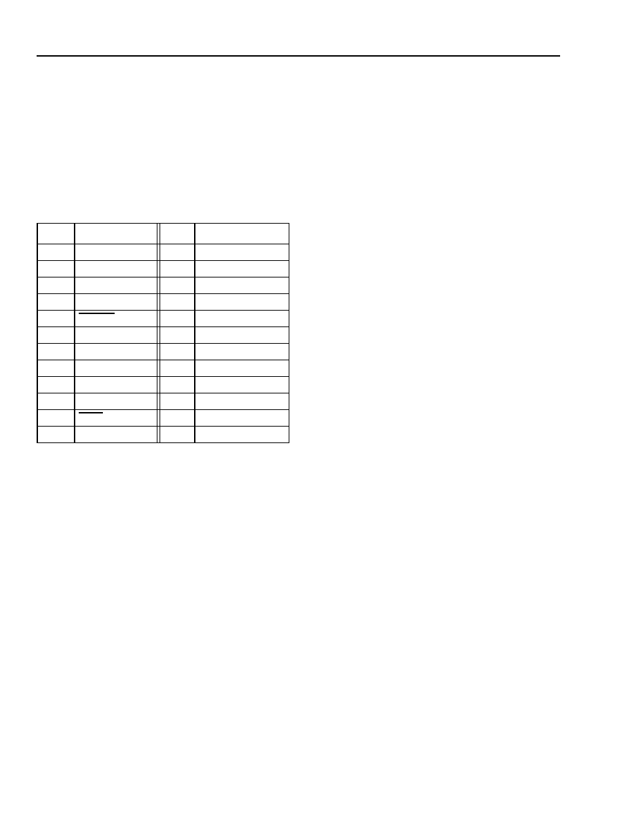
Pin Information
Table 1. Pin Information
* Pins designated as no user connect (NUC) are connected inter-
nally. The user should not make any connections to these pins.
The loss of signal (LOS) FLAG output is a logic level that indicates
the presence or absence of a minimum acceptable level of optical
input. A TTL logic HIGH indicates the absence of a valid optical
input signal.
This pin is not internally connected if the amplitude decision
threshold (DTV) is not made adjustable.
Handling Precautions
The R485-Type receiver is manufactured with a
39 in.
±
4 in. (100 cm
±
10 cm) single-mode fiber pigtail
with a 900
µ
m OD PVC outer jacket. Both SC and FC-
PC connectors are offered on standard versions. Other
optical connector options are available on special
order. Please contact an Agere Systems Account Man-
ager for availability and ordering information.
The minimum fiber bending radius is 1.5 inches
(38 mm).
Receiver Processing
The R485-Type receiver devices can withstand normal
wave soldering processes. The complete receiver mod-
ule is not hermetically sealed; therefore, it should not
be immersed in, or sprayed with, any solutions. The
optical connector process cap deformation temperature
is 85
∞
C. The receiver pins can be wave soldered at
250
∞
C for 10 seconds.
Electrostatic Discharge
CAUTION: This device is susceptible to damage as
a result of electrostatic discharge (ESD).
Take proper precautions during both
handling and testing. Follow guidelines
such as JEDEC Publication No. 108-A
(Dec. 1988).
Although protection circuitry is designed into the
device, take proper precautions to avoid exposure to
ESD.
Agere employs a human-body model HBM) for ESD-
susceptibility testing and protection design evaluation.
ESD voltage thresholds are dependent on the critical
parameters used to define the model. A standard HBM
(resistance = 1.5 k
, capacitance = 100 pF) is widely
used and, therefore, can be used for comparison pur-
poses.
Installation Considerations
Although the receiver has been designed with rugged-
ness in mind, care should be used during handling.
The optical connector should be kept free from dust.
The optical connector process cap should be kept in
place as a dust cover when the device is not connected
to a cable. If contamination is present on the optical
connector, the use of canned air with a extension tube
should remove any loose debris. Other cleaning proce-
dures are outlined in the
Cleaning Fiber Optic Assem-
blies
Technical Note (TN95-010LWP).
The cable should be handled conservatively with no
excessive axial pulling or lateral tugging.
Pin
Name
Pin
Name
1
NIC
24
NUC*
2
NUC*
23
NUC*
3
LOS Flag
22
V
CC
4
Ground
21
NUC*
5
CLOCK
20
Ground
6
CLOCK
19
Ground
7
Ground
18
NIC
8
V
CC
17
Ground
9
Ground
16
Ground
10
DATA
15
Ground
11
DATA
14
Ground
12
Ground
13
DTV/NIC
Advance Data Sheet, Rev. 1
October 2001
Recovery for 2.488 Gbits/s Applications
R485-Type Lightwave Receiver with Clock
Agere Systems Inc.
3
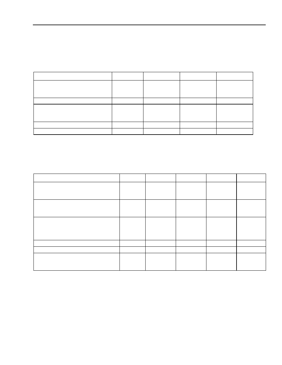
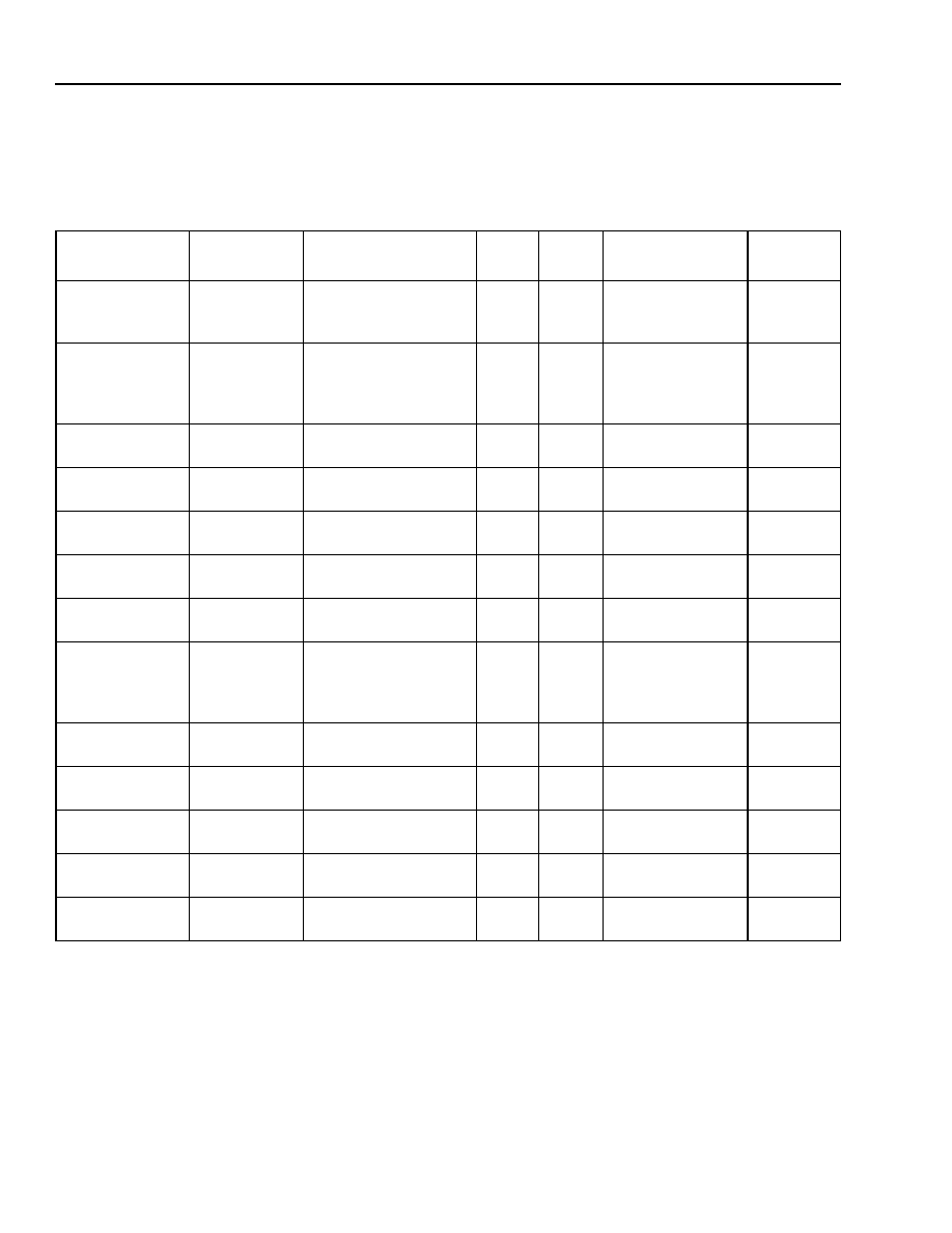
Absolute Maximum Ratings
Stresses in excess of the absolute maximum ratings can cause permanent damage to the device. These are abso-
lute stress ratings only. Functional operation of the device is not implied at these or any other conditions in excess
of those given in the operational sections of the data sheet. Exposure to absolute maximum ratings for extended
periods can adversely affect device reliability.
Characteristics
Table 2. Optical Characteristics
At 1.3
µ
m wavelength and 1 x 10
≠10
BER with 2
23
≠ 1 NRZ pseudorandom data.
* Over operating temperature range and at end of life.
Typical values at room temperature and beginning of life.
Parameter
Symbol
Min
Max
Unit
Operating Case Temperature Range:
APD
PIN
T
C
T
C
0
≠40
70
85
∞
C
∞
C
Storage Temperature
T
stg
≠40
85
∞
C
Optical Input Power--Biased:
APD
PIN
P
IN
P
IN
--
--
0
8
dBm
dBm
Supply Voltages
V
CC
0
6.5
V
Lead Soldering Temperature/Time
--
--
250/10
∞
C/s
Parameter
Symbol
Min*
Typ
Max*
Unit
Measured Average Sensitivity:
APD
PIN
P
MIN
P
MIN
--
--
≠32
≠23
≠30
≠21
dBm
dBm
Maximum Input Power:
APD
PIN
P
MAX
P
MAX
≠8
0
--
--
--
--
dBm
dBm
Link Status Switching Threshold
Decreasing Light Input:
APD
PIN
LSTD
LSTD
≠45
≠34
≠40
≠27
≠35
≠24
dBm
dBm
Flag Response Time
t
FLAG
3
--
1000
µ
s
Flag Hysteresis
--
1.2
--
--
dB
Optical Reflectance:
Single-mode Fiber
Multimode Fiber
--
--
--
--
--
≠27
≠14
dB
dB
Advance Data Sheet, Rev. 1
October 2001
Recovery for 2.488 Gbits/s Applications
R485-Type Lightwave Receiver with Clock
4
Agere Systems Inc.
Characteristics
(continued)
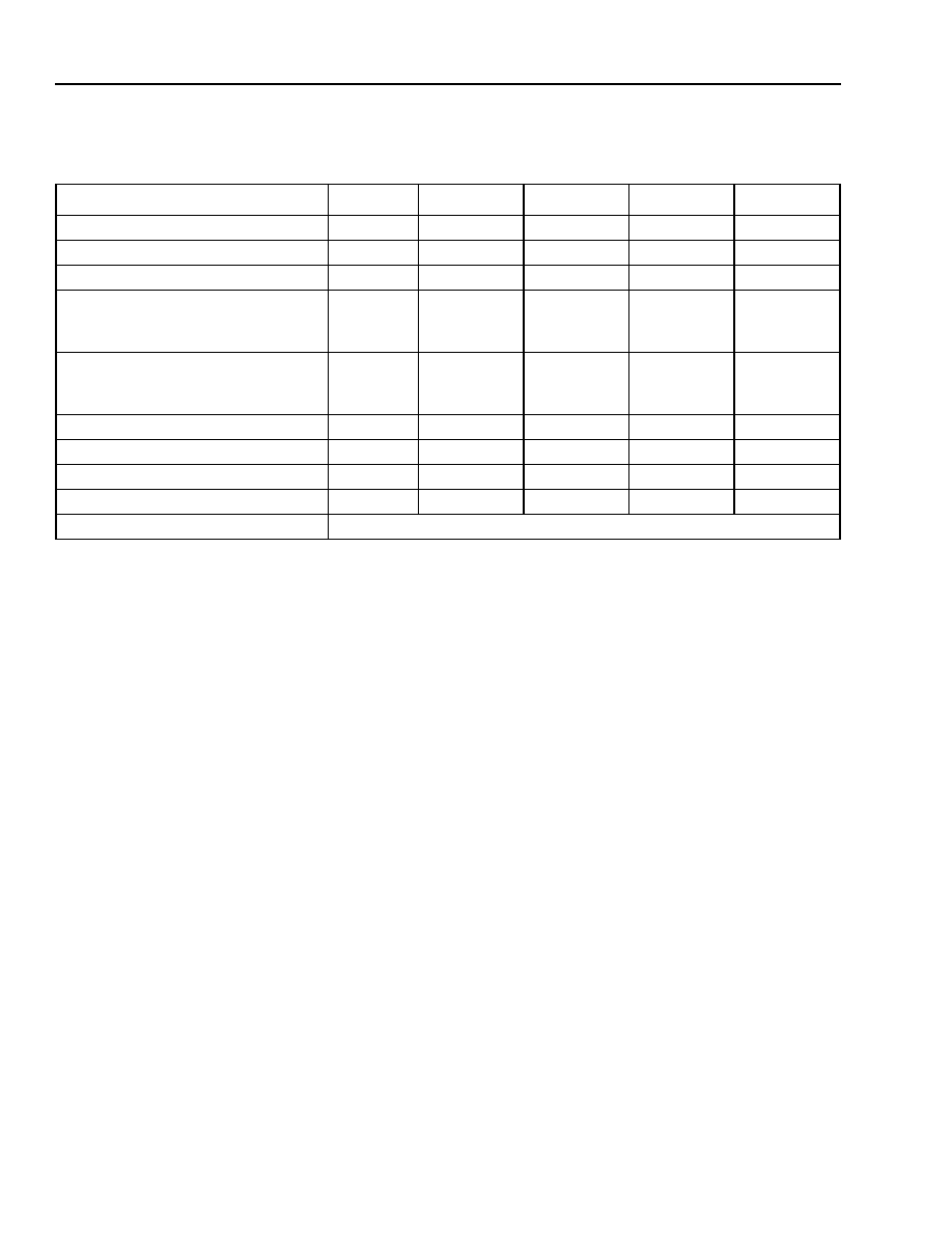
Table 3. Electrical Characteristics
* Typical values measured at room temperature and beginning of life.
Measured with a 50
to ground. Outputs must be ac-coupled (see Figure 2).
TTL output.
Parameter
Symbol
Min
Typ*
Max
Unit
Bit Rate
--
2488.07
2488.32
2488.57
Mbits/s
dc Power Supply Voltages
V
CC
4.75
5.0
5.25 V
Power Consumption
--
--
1.3
2.0
W
Output Data/Clock Voltage:
Single Output
Differential Output
SV
DV
0.3
0.6
0.4
0.8
1.0
2.0
Vp-p
Vp-p
Output Flag Voltage:
High
Low
V
FOH
V
FOL
2.5
0
5.0
0.2
V
CC
0.8
V
V
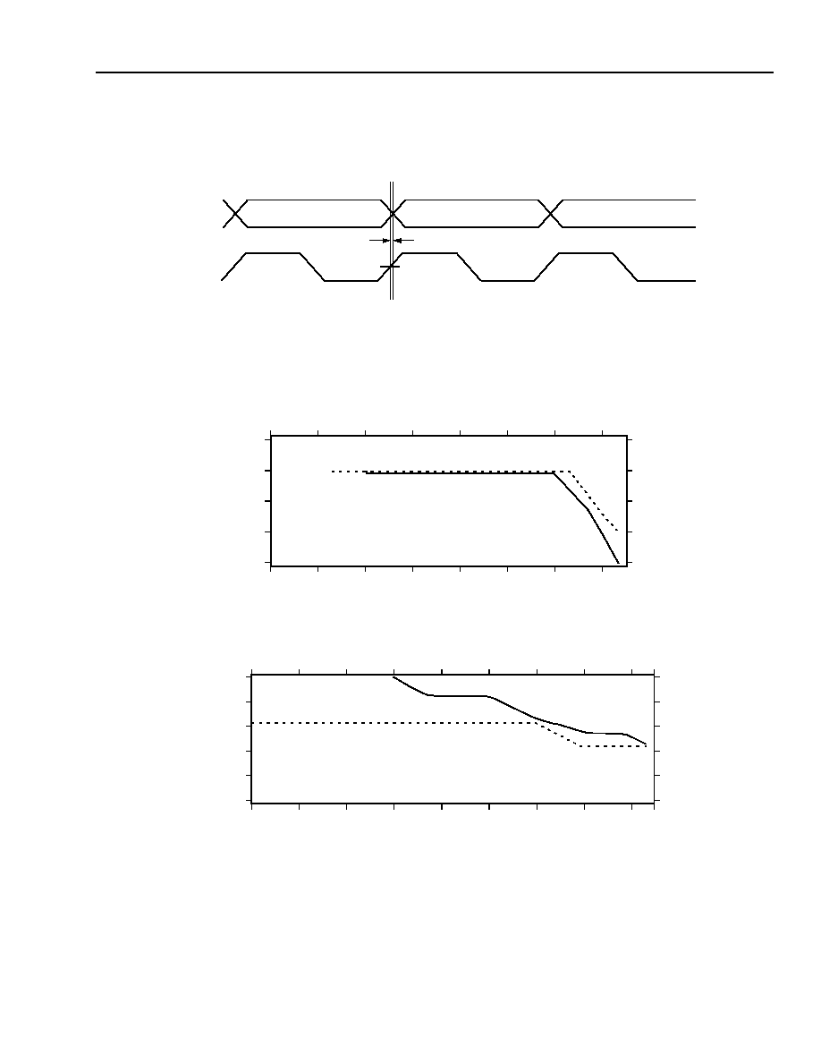
Clock/Data Alignment (see Figure 1)
t
CDA
--
0
±40
ps
Clock Duty Cycle
--
45
50
55
%
Jitter Generation
J
G
--
0.005
<0.01
Ul rms
Jitter Transfer (see Figure 2)
J
P
--
--
<0.1
dB
Jitter Tolerance (see Figure 3)
Telcordia Technologies
TM GR-253-Core and ITU-T G.958 Compliant
Advance Data Sheet, Rev. 1
October 2001
Recovery for 2.488 Gbits/s Applications
R485-Type Lightwave Receiver with Clock
Agere Systems Inc.
5
Characteristic Curves
Figure 1. Clock/Data Alignment
Figure 2. Jitter Transfer
Figure 3. Jitter Tolerance
DATA
CLOCK
50%
CLOCK/DATA ALIGNMENT
1-1313(F)
10
100
1k
10k
100k
1M
10M
(Hz)
≠30
≠20
≠10
0
10
(d
B
)
1
0.1
1
10
100
1k
10k
100k
1M
10M
(Hz)
0.001
0.01
0.1
10
100
1
(U
I
p
-p
)
1-1127(F)
1-1128(F)
Advance Data Sheet, Rev. 1
October 2001
Recovery for 2.488 Gbits/s Applications
R485-Type Lightwave Receiver with Clock
6
Agere Systems Inc.
Qualification and Reliability
The R485-type receiver is scheduled to complete the following qualification tests to meet the intent of
Telcordia
Technologies
GR-468-CORE.
Table 4. R485 Qualification Information
Test
Reference
Conditions
Code
Type
Sample
Size
Pass/Fail Criteria
Note
Mechanical Shock MIL-STD-883
Method 2002
Condition B
5 times/axis
500 G, 1 ms
R485
R480
11
Pieces
Change in Receiver
Sensitivity: ≠1.5 dB
Qualified by
T48/P172
Sine Vibration
MIL-STD-883
Method 2007
Condition A
20 G, 20 Hz--2000 Hz
4 min./cycle
4 cycles/axis
R485
R480
11
Pieces
Change in Receiver
Sensitivity: ≠1.5 dB
Qualified by
T48/P172
Thermal Shock
MIL-STD-883
Method 1011
T = 100 ∞C
R485
R480
11
Pieces
Physical Attributes
and Leak Check
Qualified by
T48/P172
Solderability
MIL-STD-883
Method 2003
(Package Supplier Test)
--
--
--
Qualified by
T48
Lead
Integrity
MIL-STD-883
Method 2004
(Package Supplier Test)
--
--
--
Qualified by
T48
Solvent
Resistance
MIL-STD-883
Method 2015
(Package Supplier Test)
--
--
--
Qualified by
T48
Fiber Pull
GR-468-CORE
Table 6
1 kg; 3 times; 5 s
R485
R480
11
Pieces
Change in Receiver
Sensitivity: ≠1.5 dB
Qualified by
P172
Accelerating
Aging
(HTOB)
MIL-STD-883
Method 1005
85 ∞C under bias,
2000 hours
R485
R480
25
Pieces
Change in Receiver
Sensitivity: ≠1.5 dB
Qualified by
T48/P172;
Refer to
Chip Data
High Temperature
Storage
GR-468-CORE
Table 6
85 ∞C storage,
2000 hours
R485
R480
11
Pieces
Change in Receiver
Sensitivity: ≠1.5 dB
Qualified by
T48/P172
Temperature
Cycling
GR-468-CORE
Section 5.20
≠40 ∞C to +85 ∞C
100 Cycles for Pass/Fail
R485
R480
11
Pieces
Change in Receiver
Sensitivity: ≠1.5 dB
Qualified by
T48/P172
Temperature
Humidity Bias
GR-468-CORE
Table 6
85 ∞C/85% RH
1000 hours
R485
R480
11
Pieces
Change in Receiver
Sensitivity: ≠1.5 dB
Qualified by
T48/P172
Internal Water
Vapor
MIL-STD-883
Method 1018
5000 ppm Water Vapor
R485
R480
11
Pieces
Change in Receiver
Sensitivity: ≠1.5 dB
Qualified by
T48/P172
ESD
GR-468-CORE
Section 5.22
Human-Body Model
R485
R480
6
Pieces
Threshold
Minimum: 500 V
--
Advance Data Sheet, Rev. 1
October 2001
Recovery for 2.488 Gbits/s Applications
R485-Type Lightwave Receiver with Clock
Agere Systems Inc.
7
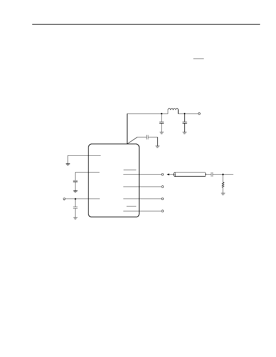
PWB Layout Guidelines
s
The data and clock outputs are designed to drive 50
loads.
s
Clock and data output traces must be controlled-impedance lines and the termination impedance must match
the line impedance. Avoid 90
∞
bends in the traces. Paired lines (i.e., DATA and DATA) must be equal in length.
s
Data and clock output lines should be as short and straight as possible and should be shielded from noise
sources to prevent noise from feeding back into the receiver.
s
Use high-quality multilayer printed-wiring boards. A ground plane should occupy the area directly beneath the
receiver.
1-934(F)xxx
Note 1: Data and clock outputs must be ac-coupled on customer board. Use a 0.1
µ
F chip capacitor with a low ESR. For optimum receiver per-
formance, all four outputs must be terminated in equivalent loads, even if some of the outputs are not being used.
Note 2: The 0.1
µ
F V
CC
power supply bypass capacitors should be high-quality, low ESR chip capacitors that are located as close as possible to
the appropriate power supply leads and should provide a low inductance path to the ground plane.
Figure 4. Biasing and Interfacing to the R485-Type 2.5 Gbits/s Receiver
8, 22
5
6
10
11
CLOCK
CLOCK
DATA
DATA
50
TRANSMISSION
4, 7, 9, 12,
2.2
µ
F
15
µ
F
+5 V
0.1
µ
F
50
+
14--17, 19, 20
LINE (4X)
V
CC
1
µ
H
0.1
µ
F
NOTE 2
NOTE 1
LOS (FLAG)
3
0.1
µ
F
NIC
1
0.1
µ
F
Advance Data Sheet, Rev. 1
October 2001
Recovery for 2.488 Gbits/s Applications
R485-Type Lightwave Receiver with Clock
8
Agere Systems Inc.
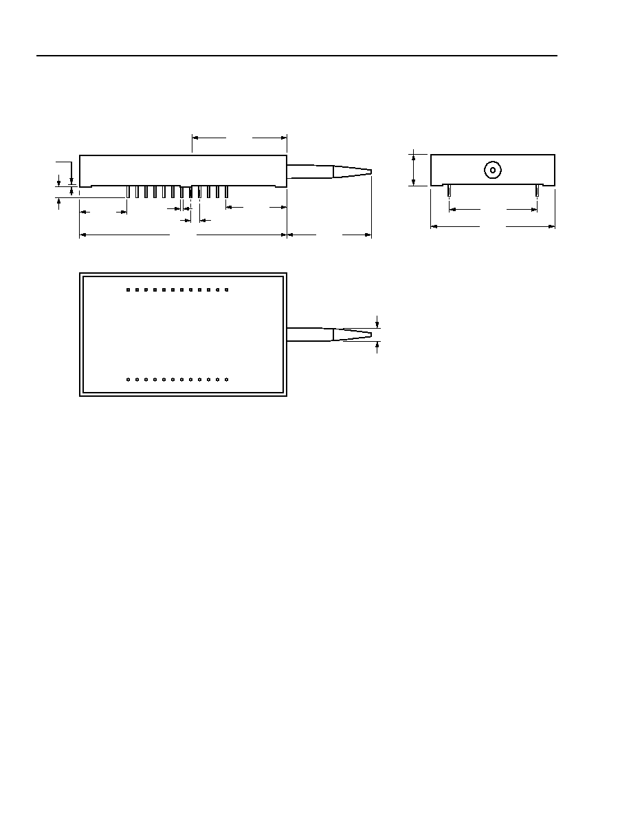
Outline Diagrams
Dimensions are in inches and (millimeters).
1-999(F)
1.100
(27.94)
0.495
(12.57)
0.018
(0.48)
0.100
(2.54)
0.710
(18.03)
2.305
(58.55)
0.950
(24.13)
0.122
(3.10)
0.014
(0.36)
13
24
12
1
0.144
(3.36)
BOTTOM VIEW
0.350
(8.89)
1.000
(25.40)
1.400
(35.56)
Advance Data Sheet, Rev. 1
October 2001
Recovery for 2.488 Gbits/s Applications
R485-Type Lightwave Receiver with Clock
Agere Systems Inc.
9
Ordering Information
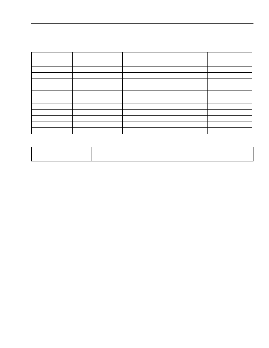
Table 5. Ordering Information for the R485-Type Receiver
Table 6. Related Product Information
Code
Detector Type
Connector Type
Fiber Type
Comcode
R485CMAA
APD
SC/PC
Single-Mode
108514597
R485FMAA
APD
FC/PC
Single-Mode
108514613
R485WMAA
APD
LC
Single-Mode
TBD
R485JMAA
APD
MU
Single-Mode
TBD
R485CPAA
PIN
SC/PC
Single-Mode
108514605
R485FPAA
PIN
FC/PC
Single-Mode
108514621
R485WPAA
PIN
LC
Single-Mode
TBD
R485JPAA
PIN
MU
Single-Mode
TBD
R485CPBB
PIN
SC/PC
Multimode
TBD
R485FPBB
PIN
FC/PC
Multimode
TBD
R485WPBB
PIN
LC
Multimode
TBD
R485JPBB
PIN
MU
Multimode
TBD
Product Code
Description
Document Number
T48 Transmitter
2.5 Gbits/s Uncooled Laser Transmitter
DS00-088OPTO

Advance Data Sheet, Rev. 1
October 2001
Recovery for 2.488 Gbits/s Applications
R485-Type Lightwave Receiver with Clock
Agere Systems Inc. reserves the right to make changes to the product(s) or information contained herein without notice. No liability is assumed as a result of their use or application.
Copyright © 2000 Agere Systems Inc.
All Rights Reserved
Printed in U.S.A.
October 2001
DS01-005OPTO-1 (Replaces DS01-005OPTO)
For additional information, contact your Agere Systems Account Manager or the following:
INTERNET:
http://www.agere.com
E-MAIL:
docmaster@agere.com
N. AMERICA:
Agere Systems Inc., 555 Union Boulevard, Room 30L-15P-BA, Allentown, PA 18109-3286
1-800-372-2447, FAX 610-712-4106 (In CANADA: 1-800-553-2448, FAX 610-712-4106)
ASIA:
Agere Systems Hong Kong Ltd., Suites 3201 & 3210-12, 32/F, Tower 2, The Gateway, Harbour City, Kowloon
Tel. (852) 3129-2000, FAX (852) 3129-2020
CHINA: (86) 21-5047-1212 (Shanghai), (86) 10-6522-5566 (Beijing), (86) 755-695-7224 (Shenzhen)
JAPAN: (81) 3-5421-1600 (Tokyo), KOREA: (82) 2-767-1850 (Seoul), SINGAPORE: (65) 778-8833, TAIWAN: (886) 2-2725-5858 (Taipei)
EUROPE:
Tel. (44) 7000 624624, FAX (44) 1344 488 045
Telcordia Technologies
is a trademark of Telcordia Technologies Inc.