 | –≠–ª–µ–∫—Ç—Ä–æ–Ω–Ω—ã–π –∫–æ–º–ø–æ–Ω–µ–Ω—Ç: T7121 | –°–∫–∞—á–∞—Ç—å:  PDF PDF  ZIP ZIP |

Data Sheet
April 1997
T7121 HDLC Interface for ISDN (HIFI-64)
Features
s
Low-cost device for B-channel (64 kbits/s) or
D-channel (16 kbits/s) data transport.
s
Optional transparent mode--no HDLC framing is
performed.
s
Frame sync (FS) allows a slot-select feature to
access an individual time slot in any TDM data
stream (e.g., Lucent Technologies Microelectronics
Group Concentration Highway Interface [CHI] or
subset).
s
Bit-masking option allows effective data rates of 8,
16, 24, 32, 40, 48, and 56 kbits/s.
s
Maximum data rate up to 4.096 MHz.
s
Serial data-transfer pins for direct connection to the
Lucent ISDN line transceiver T7250C.
s
Supports IOM2, K2, GCI, and SLD interface.
s
Parallel microprocessor interface with either multi-
plexed or demultiplexed address and data lines for
easy interface with any microprocessor.
s
Single interrupt output signal with seven maskable
interrupt conditions.
s
Programmable interrupt modes.
s
Memory-mapped read and write registers.
s
TTL/CMOS compatible input/output.
s
3-state output pins to assist system diagnostics.
s
Low-power 1.25
µ
m CMOS:
-- 30 mW typical operation at 12 MHz.
-- 5 mW standby mode (typical).
s
HDLC transceiver:
-- Stand-alone HDLC framing operation.
-- 64-byte FIFO in both transmit and receive direc-
tions.
-- Supports block-move instruction.
-- Multiple frames allowed in FIFO.
-- Programmable FIFO full- and empty-level inter-
rupt.
Description
The T7121 HDLC Interface for ISDN (HIFI-64) con-
nects serial communications links carrying HDLC bit-
synchronous data frames to 8-bit microcomputer sys-
tems. There is an optional transparent mode of oper-
ation in which no HDLC processing is performed on
user data. The device communicates with the system
microprocessor as a memory-mapped peripheral and
is controlled by reading and writing 19 internal regis-
ters. The chip can be instructed to interrupt the
microprocessor when it detects certain events requir-
ing microprocessor attention. The HDLC transmitter
and receiver are each buffered with 64-byte, first-in-
first-out (FIFO) memory storage. The 64-byte buffer
depth reduces the number of status polls or inter-
rupts to be processed by the microprocessor, improv-
ing overall system efficiency. The major blocks are
the microprocessor interface, transmit and receive
FIFO memory buffers, HDLC processor, and a con-
centration highway interface (see Figure 1). The
T7121 device is available in a 28-pin, plastic DIP or a
28-pin, plastic, small-outline, J-lead (SOJ) package
for surface mounting.

Table of Contents
Contents
Page
2
Lucent Technologies Inc.
Data Sheet
April 1997
T7121 HDLC Interface for ISDN (HIFI-64)
Features ................................................................................................................................................................... 1
Description................................................................................................................................................................ 1
Pin Information ......................................................................................................................................................... 4
Functional Description .............................................................................................................................................. 8
Microprocessor Bus Interface ................................................................................................................................ 8
Addressing .......................................................................................................................................................... 8
Interrupts ............................................................................................................................................................. 8
Resets ................................................................................................................................................................. 9
FIFO Memory Buffers ............................................................................................................................................ 9
Transmit FIFO ..................................................................................................................................................... 9
Receive FIFO .................................................................................................................................................... 10
Block Move........................................................................................................................................................ 10
Serial Link Interface .......................................................................................................................................... 10
Enabling the Transmitter and Receiver ............................................................................................................. 10
Time-Slot Feature ............................................................................................................................................. 13
Transmission During Unassigned Time Slots ................................................................................................... 14
Bit Order During Transmission .......................................................................................................................... 14
Bit Masking........................................................................................................................................................ 16
SLD and IOM2 Examples.................................................................................................................................. 19
HDLC Operation .................................................................................................................................................. 19
Zero-Bit Insertion/Deletion (Bit Stuffing/Destuffing) .......................................................................................... 19
Transmitter FIFO ............................................................................................................................................... 21
Sending 1-Byte Frames .................................................................................................................................... 21
Transmitter Underrun ........................................................................................................................................ 21
Using the Transmitter Status and Fill Level ...................................................................................................... 21
Receiver FIFO ................................................................................................................................................... 21
Receiver Overrun .............................................................................................................................................. 23
Operational Note (T7121-EL, T7121-PL, T7121-EL2, and T7121-PL2) ............................................................ 23
Transparent Mode................................................................................................................................................ 24
Diagnostic Modes ................................................................................................................................................ 25
Loopbacks ......................................................................................................................................................... 25
3-State Mode..................................................................................................................................................... 28
Other ................................................................................................................................................................. 28
Powerdown Mode ................................................................................................................................................ 28
Registers.............................................................................................................................................................. 28
Absolute Maximum Ratings.................................................................................................................................... 45
Electrical Characteristics ........................................................................................................................................ 45
Clock Characteristics.............................................................................................................................................. 46
Timing Characteristics ............................................................................................................................................ 46
TDM Frame Timing Diagrams.............................................................................................................................. 46
Multiplexed Address and Data ............................................................................................................................. 51
Separate Address and Data................................................................................................................................. 53
Concentration Highway........................................................................................................................................ 55
Handling Precautions ............................................................................................................................................. 59
Outline Diagrams.................................................................................................................................................... 60
28-Pin, Plastic DIP ............................................................................................................................................... 60
28-Pin, Plastic SOJ, Surface Mounting................................................................................................................ 61
Ordering Information............................................................................................................................................... 62
Appendix................................................................................................................................................................. 63
Transparent Mode................................................................................................................................................ 63
HDLC Mode ......................................................................................................................................................... 63
General Features ................................................................................................................................................. 64
Power and Ground............................................................................................................................................... 66
Lucent Technologies Inc.
3
Data Sheet
April 1997
T7121 HDLC Interface for ISDN (HIFI-64)
Description
(continued)
5-5027
Figure 1. Block Diagram
MICRO-
PROCESSOR
BUS
INTERFACE
INTERNAL
REGISTER
BANK
(R0--R15)
(AR11--AR13)
AND
PARALLEL
DATA I/O
MEMORY
BUFFERS
HDLC
PROCESSING
TRANSPARENT
MODE
TRANSMIT
FIFO
64 x 8
RECEIVE
FIFO
64 x 8
HDLC
TRANSMITTER
HDLC
RECEIVER
CONCEN-
TRATION
HIGHWAY
INTERFACE
TRANSPARENT
MODE
RESET
RD
WR
CS
INT
AD0--AD7
ALE
A0--A3
DXA
DXB/TSCA
CLKX
CLK
FS
DRA
CLKR/DRB
4
Lucent Technologies Inc.
Data Sheet
April 1997
T7121 HDLC Interface for ISDN (HIFI-64)
Pin Information
5-5028
Figure 2. Pin Diagram
Table 1. Pin Assignments
Group
Symbol
Function
Chip Clock
CLK
0 MHz--12 MHz
Power & Ground
V
DD
V
SS
5 V Power
Ground
Microprocessor Bus Interface
RD
WR
CS
INT
RESET
AD7--AD0
ALE
A3--A0
Read
Write
Chip Select
Interrupt
Reset
Address/Data Bus
Address Latch Enable
Address Bus (non-ALE addressing mode)
Serial Link Interface
DXA
DXB
TSCA
CLKX
FS
CLKR
DRA
DRB
Transmit Data A
Transmit Data B
Time-slot Control DXA
Transmit Clock
Frame Synchronization
Receive Clock
Receive Data A
Receive Data B
ALE
AD0
AD1
AD2
AD3
AD4
AD5
AD6
AD7
RD
CS
INT
1
2
3
4
5
6
7
8
9
10
11
12
13
14
V
DD
A2
A3
CLKR/DRB
DXA
CLKX
DXB/TSCA
FS
RESET
28
27
26
25
24
23
22
21
20
19
18
17
16
15
V
SS
WR
A0
CLK
V
SS
DRA
LUCENT
T7121
HIFI-64
A1
Lucent Technologies Inc.
5
Data Sheet
April 1997
T7121 HDLC Interface for ISDN (HIFI-64)
Pin Information
(continued)
Table 2. Pin Descriptions
Pin
Symbol
Type
Name/Function
1
ALE
I
Address Latch Enable.
A high-to-low transition on this pin latches the register
address on pins AD3--AD0. ALE should be held high in the demultiplexed (sep-
arate address/data) mode. ALE latches the address regardless of the state of
CS
.
2--5,
7--10
AD0--AD7
I/O
Address/Data Bus.
The data bus direction is controlled by the logic states of
the
CS
,
RD
, and
WR
pins. Microprocessors using a multiplexed bus supply
address information during read or write cycles on AD6, AD3--AD0 synchro-
nized to the ALE signal. During read cycles, data is available to the micropro-
cessor on AD7--AD0. During write cycles, data is supplied by the
microprocessor on these lines. When
CS
is not active, the AD7--AD0 pins are
placed in a high-impedance state (3-state). AD0 is the least significant
address/data bit.
Block move is available in MUXed address and data mode by setting the BM bit
in register 0 (R0--B3) to 1 and holding AD6 high during the address cycle of the
ALE. All writes then go directly to the transmit FIFO, and all reads address the
receive FIFO. Normal ALE mode addressing is accomplished by holding AD6
low during the ALE address cycle. Block move can be disabled by clearing the
BM bit to 0.
6, 22
V
SS
--
Ground.
11
WR
I
Write (Active-Low).
This signal controls when data is written to the registers.
When
CS
and
WR
are low, valid data is supplied on lines AD7--AD0 by the
microprocessor. The chip latches the data on the rising edge of
WR
.
12
RD
I
Read (Active-Low).
This signal is used to read data from the registers. When
CS
and
WR
are low, the chip makes the requested data available on lines AD7--
AD0 to be read by the microprocessor.
13
CS
I
Chip Select (Active-Low).
This signal must be low for the internal registers to
be read or written.
14
INT
O
Interrupt.
An interrupt signal is generated when any of the interrupting condi-
tions are true. The interrupt signal remains active until the microprocessor reads
the interrupt status register (R15) if DINT (R0--B0) = 0, or until the condition
causing the interrupt is alleviated if DINT = 1. Interrupts can be masked by
appropriately setting the corresponding interrupt enable bits in the interrupt
mask register (R14). The polarity of the interrupt signal output is controlled by
the IPOL bit in register 0 (R0--B1). This pin is
not
an open-drain output.
15
RESET
I
Reset.
A high on this pin resets the device and forces a high-impedance
(3-state) condition on all outputs. All register bits are forced to their reset values.
(See Register section for more details.) A reset must be performed upon pow-
erup. A full chip reset occurs with or without a clock input.
16
FS
I
Frame Synchronization.
This signal marks the beginning of a TDM highway
frame. The polarity of the input pulse can be adjusted via the FSPOL bit in regis-
ter 0 (R0--B6). Individual time slots are assigned relative to the detection of FS
by the use of registers 7--11. When HWYEN (R0--B7) is 0, the input to this pin
is ignored.

6
Lucent Technologies Inc.
Data Sheet
April 1997
T7121 HDLC Interface for ISDN (HIFI-64)
17
DXB/
TSCA
O
Transmit Data B or Time-Slot Control for DXA.
The functionality of this pin is
user-controlled by the P17CTL bit in the receiver control register (R5--B7).
Clearing the P17CTL bit to 0 selects operation as Transmit Data B. Once DXB
operation is selected, data is transmitted on DXB whenever the DXBC bit in reg-
ister 7 (R7--B6) is set to 1. Data can be configured for transmission on either
CLKX edge (CLKXI, R9--B4), optionally inverted (DXI, R10--B7) and placed in
a user-selected time slot (registers 7, 9, 10) with bit 0 or bit 7 sent first (TLBIT,
R10--B6).
DXB should be pulled up by an external resistor to prevent random data pat-
terns from propagating through other devices when DXB is 3-stated.
When P17CTL (R5--B7) is set to 1, this pin is configured as
TSCA
(active-low)
(time-slot control for DXA).
TSCA
allows use of an external 3-stating bus driver
when data is being transmitted on DXA over long distances.
TSCA
goes low dur-
ing the valid bit positions of data and is high at all other times.
When an external driver is required, DXAC (R7--B7) must be set to 1. Setting
the P17CTL bit (R5--B7) to 1 overrides the selection of DXBC (R7--B6).
18
CLKX
I
Transmit Clock.
This input clock controls the bit rate for transmitted data. Trans-
mit clock frequency must be less than the chip master clock frequency divided
by 2 (fCLKX < fCLK/2). In the reset configuration, data is transmitted on the fall-
ing edge of CLKX. Data can be transmitted by using the rising edge of CLKX by
setting the CLKX Invert bit (CLKXI) in the bit offset register (R9--B4) to 1. If the
P21CTL bit in the receiver control register (R5--B6) is set to 1, this clock is also
used to receive data. If P21CTL is 0, the transmit clock rate can be independent
of the receive clock rate.
19
DXA
O
Transmit Data A.
When the DXAC bit in register 7 (R7--B7) is set to 1, data is
transmitted on this pin. If external drivers are not required, both DXAC (R7--B7)
and DXBC (R7--B6) can be set to allow simultaneous transmission of the data
byte on both transmit data pins.
Data can be configured for transmission on either CLKX edge (CLKXI, R9--B4),
optionally inverted (DXI, R10--B7) and placed in a user-selected time slot (reg-
isters 7, 9, 10) with bit 0 or bit 7 sent first (TLBIT, R10--B6).
DXA should be pulled up by an external resistor to prevent random data pat-
terns from propagating through other devices when DXA is 3-stated.
20
DRA
I
Receive Data A.
When the DRA/B bit in register 8 (R8--B7) is cleared to 0,
data is received on this pin. Data can be optionally inverted (DRI, R11--B7),
received on a positive or negative receive clock edge (CLKRI, R9--B0), and
received during a user-selected time slot (registers 8, 9, 11) with bit 0 or bit 7
first (RLBIT, R11--B6).
Table 2. Pin Descriptions
(continued)
Pin
Symbol
Type
Name/Function
Pin Information
(continued)

Lucent Technologies Inc.
7
Data Sheet
April 1997
T7121 HDLC Interface for ISDN (HIFI-64)
21
CLKR/DRB
I
Receive Clock or Receive Data B.
The functionality of this pin is controlled by
programming the P21CTL bit in the receiver control register (R5--B6). When
P21CTL is cleared to 0 (default), this pin is the receive data clock (CLKR).
Receive clock frequency must be less than the chip master clock frequency
divided by 2 (fCLKR < fCLK/2). Upon reset, data is received (latched) on the ris-
ing edge of CLKR. Data can be received on the falling edge of the receive clock
by clearing the CLKRI bit in register 9 (R9--B0) to 0. Receive clock rate can be
independent of transmit clock rate.
When P21CTL (R5--B6) is set to 1, this pin is configured as Receive Data B
(DRB). Clocking for receive data is obtained from CLKX, while CLKRI (R9--B0)
controls the edge of CLKX used to latch received data. In this mode, data can
be received on DRA or on DRB. DRB is selected by setting the DRA/B bit in reg-
ister 8 (R8--B7) to 1. Data can be optionally inverted (DRI, R11--B7) and
received during a user-selected time slot (registers 8, 9, 11) with bit 0 or bit 7
first (RLBIT R11--B6).
23
CLK
I
Clock.
This clock controls internal chip operation. It can be from 0 MHz to
12 MHz. Typically it is 6.144 MHz (i.e., SYSCKO from the Lucent T7250C).
Clock frequency must be greater than two times the fastest data clock fre-
quency.
24, 25, 26,
27
A3--A0
I
Address Bus.
These four address leads allow the chip to be accessed by a
microprocessor employing separate address and data leads. They are used to
select the internal registers. The ALE pin should be tied high in this mode of
operation.
These pins can be left unconnected when in the multiplexed address/data mode
(internal pull-up resistors are provided).
28
V
DD
--
+5 V Supply.
Table 2. Pin Descriptions
(continued)
Pin
Symbol
Type
Name/Function
Pin Information
(continued)

8
8
Lucent Technologies Inc.
Data Sheet
April 1997
T7121 HDLC Interface for ISDN (HIFI-64)
Functional Description
Microprocessor Bus Interface
Addressing
The T7121 is designed to easily interface with 8-bit
microprocessors. The microprocessor bus interface
allows parallel asynchronous access to a bank of 19
registers (R0--R15 and AR11--AR13). The bus inter-
face is compatible with most microprocessors. The reg-
isters occupy 16 continuous locations in the memory
map of a controlling microprocessor, and the registers
are accessed under the control of the following signals:
address select (A0--A3 or AD0--AD7), address latch
enable (ALE), chip select (
CS
), read (
RD
), and write
(
WR
). When multiplexed address and data lines are
used, the ALE signal is used to latch the address
present on AD0--AD3 and AD6. AD6 has a special
use in the block-move mode. See the Block Move sec-
tion under the FIFO Memory Buffers section. ALE
should be tied high when separate address and data
are used.
Registers 11, 12, and 13 have alternate meanings
depending on the value of the Alternate (ALT) bit in the
chip configuration register (R0--B4). The alternate reg-
isters are accessed by setting the ALT bit (R0--B4) to
1. All subsequent addressing of registers 11 through 13
then refers to the alternate registers (AR11--AR13).
Returning to the foreground register set is accom-
plished by clearing the ALT bit (R0--B4) to 0.
Interrupts
A programmable interrupt output, INT, is provided to
alert the microprocessor when the device needs ser-
vice. Associated with the interrupt system are the IPOL
bit in register 0 (R0--B1), the interrupt mask register
(R14), and the interrupt status register (R15). The
polarity of the INT signal (pin 14) is programmable by
setting the IPOL bit in register 0 (R0--B1). The inter-
rupt mask register can be programmed so that only
certain conditions cause the INT signal to be asserted.
The interrupt status register (R15) reveals the source of
the interrupt.
Register 14, the interrupt mask register, controls the
operation of the INT pin. Masking an interrupt means
that no transition of the INT pin is generated for any
occurrence of that interrupt condition. The INT signal is
enabled upon the first occurrence of any unmasked
interrupt condition. The INT signal remains until the
interrupt is acknowledged by reading the interrupt sta-
tus register (R15). Unmasked interrupts occurring
between the first unmasked interrupt and the status
register read do not cause a transition of the INT pin. If
a second interrupt occurs during a read of the interrupt
status register (R15), the INT signal is disabled after
the read and then reasserts itself. This deassertion can
actually be much less than one cycle, and no minimum
width is guaranteed. One method to ensure that the
second interrupt is detected is to use an edge-sensed
INT pin on the processor. If this is not available, the
interrupt service routine should reread the interrupt sta-
tus register to determine if an interrupt occurred during
the clearing of the first interrupt.
Masking all interrupts effectively disables the INT pin. It
is possible to mask a currently active interrupt. Doing
so causes a transition of the INT pin from active to
inactive if the masked interrupt was the only active
interrupt. Likewise, unmasking an interrupt that is cur-
rently asserted causes an INT pin transition from inac-
tive to active if all other unmasked interrupts were
currently inactive. Interruptable conditions are always
reported in register 15, even if the interrupt pin transi-
tion is masked. Thus, polled interrupt systems are also
supported. Note that a transition of the INT pin occurs
only if the interrupting condition is unmasked and no
other unmasked, unacknowledged interrupt exists.
The HIFI-64 allows two modes of interrupt: dynamic
and nondynamic. The mode is controlled by setting the
DINT (Dynamic INTerrupt) bit in register 0 (R0--B0). If
DINT (R0--B0) is 0 (nondynamic mode), the interrupt
bits in the interrupt status register (R15) are cleared
directly by a read of register 15. The condition causing
the interrupt must go away and come back in order to
reassert the interrupt. If DINT (R0--B0) is set to 1
(dynamic mode), the transmitter empty (R15--B1) and
receiver full (R15--B3) interrupts are cleared only
when the condition causing the interrupt has been rem-
edied (all other interrupts are cleared by reading the
interrupt status register [R15]). In addition, the INT sig-
nal (pin 14) remains enabled until the condition(s)
causing the interrupt has been remedied.
A dynamic version of the transmitter empty interrupt,
transmitter empty dynamic (TED), is provided in the
transmitter status register (R2--B7). TED behaves
dynamically regardless of the value of the DINT bit
(R0--B0). TED does not cause a transition of the INT
pin.
In transparent mode, the REOF, RIDL, and UNDABT
interrupts are disabled. TDONE is used to indicate a
transmitter underrun and can be used to determine
transmission end. Additionally, the MSTAT bit
(AR11--B3) can be used as a polled interrupt to deter-
mine the beginning of receive data. A transition of the
INT pin can be programmed for the beginning of
receive data by setting the initial receiver-full interrupt
level RIL (R5--B[5--0]) to 1 byte.

Lucent Technologies Inc.
9
Data Sheet
April 1997
T7121 HDLC Interface for ISDN (HIFI-64)
Functional Description
(continued)
Resets
The T7121 is fully reset by either asserting the RESET
pin (hardware reset) or by asserting both the TRES
(R6--B5) and RRES (R6--B4) bits simultaneously
when writing to register 6 (software reset). A full reset
results in all registers returning to their default condi-
tions and all logic returning to a known state. No clock
input is necessary. During a hardware reset, all outputs
are 3-stated. Thus, the RESET pin can be used for
bed-of-nails testing. During a software reset, outputs
are not automatically 3-stated. Output pin states are
determined by their default register configuration. Both
transmit data pins (DXA and DXB) 3-state since the
default register configuration is both transmit pins dis-
abled. The INT pin is high.
In addition, the transmitter and receiver can be individ-
ually reset. When TRES (R6--B5) is high and RRES
(R6--B4) is low during a write of register 6, the trans-
mitter is independently reset. The transmitter FIFO
pointers return to default values, resulting in the loss of
any untransmitted data, and the transmitter state
machine is returned to the idle state. Transmitter inter-
rupts are cleared, except for the TE (R15--B1) inter-
rupt, which is asserted and causes a transition on the
INT pin if unmasked (TEIE, R14--B1 = 1). Only trans-
mit status registers and interrupts change to reflect the
reset. Disabling the transmitter does not cause an
automatic reset. When the transmitter has been active
and then subsequently disabled, a TRES is needed to
restore it to a known state.
When TRES (R6--B5) is low and RRES (R6--B4) is
high during a write of register 6, the receiver is inde-
pendently reset. A receiver reset causes the receiver
FIFO pointers to return to their default values, resulting
in the loss of unread data in the FIFO. The receiver is
returned to a known state, and all currently asserted
receiver interrupts are cleared. The receiver should be
reset whenever it was active and subsequently dis-
abled to ensure correct operation. Only receiver status
and interrupt bits are affected in the register set. Dis-
abling the receiver does not cause a receiver reset.
FIFO Memory Buffers
The HIFI-64 is equipped with a transmit FIFO and a
receive FIFO, each with a capacity of 64 bytes.
Transmit FIFO
Data to be transmitted is loaded via the data register
(R3) into the 64-byte transmit FIFO. Multiple frames
can be placed in the FIFO. In HDLC mode, the final
byte of each frame is marked by writing the transmit
frame complete bit TFC (R1--B7). The transmitter can
also be instructed to abort a frame by using the trans-
mit abort bit TABT (R1--B6) (HDLC mode only). Trans-
mission status is available in the transmit status
register and via the transmit interrupts. The transmitter
status register (R2) indicates how many additional
bytes can be added to the FIFO. The transmitter inter-
rupt trigger level (TIL) can be programmed in the trans-
mitter control register (R1--B[5--0]) to tailor service
time intervals to the system environment. The transmit-
ter empty (TE) interrupt bit is set in the interrupt status
register (R15--B1) when the FIFO has sufficient empty
space to add the number of bytes specified in the TIL. If
the TE interrupt mask TEIE (R14--B1) is 1, the occur-
rence of a TE interrupt condition causes a transition of
the interrupt pin if no other unmasked interrupts are
currently active. In dynamic interrupt mode (DINT,
R0--B0 = 1), this interrupt remains set until the condi-
tion is cleared. In nondynamic interrupt mode
(DINT, R0--B0 = 0), this interrupt is cleared by reading
R15. A TDONE (R15--B0) interrupt occurs for each
HDLC frame completed. In the transparent mode, a
TDONE interrupt occurs when the transmit FIFO emp-
ties. In HDLC mode, an UNDABT (R15--B2) interrupt
is issued if the transmitter underruns.
There is no interrupt indication of a transmitter overrun
that is writing more data than empty spaces exist.
Overrunning the transmitter causes the last valid data
byte written to be repeatedly overwritten, resulting in
missing data in the frame.

10
10
Lucent Technologies Inc.
Data Sheet
April 1997
T7121 HDLC Interface for ISDN (HIFI-64)
Functional Description
(continued)
Receive FIFO
Data received from the serial link interface is stored in
the 64-byte receive FIFO. In the HDLC mode, the
receiver also places a status of frame (SF) status byte
in the receiver FIFO for every completed frame
received. Whenever an SF frame status byte is present
in the receive FIFO, the EOF bit (R4--B7) is set. The
receiver queue status (RQS) bits (R4--B[6--0]) report
the number of bytes up to and including the first SF
frame status byte. If no SF frame status byte is present
in the FIFO (EOF, R4--B7 = 0), the count directly
reflects the number of data bytes available to be read.
Depending on frame size, it is possible for multiple
frames to be present in the FIFO. The receiver fill level
indicator (RIL) can be programmed in the receiver con-
trol register (R5--B[5--0]) to tailor the service time
interval to the system environment. The receiver full
(RF) interrupt bit is set in the interrupt status register
(R15--B3) when the FIFO reaches the prepro-
grammed full position. The RF interrupt condition is
reported in the interrupt register (R15--B3). If the RF
interrupt mask RFIE (R14--B3) is 1, the occurrence of
an RF interrupt condition causes a transition of the
interrupt pin if no other unmasked interrupts are
present. In dynamic interrupt mode (DINT,
R0--B0 = 1), this interrupt remains set until the condi-
tion is cleared. In nondynamic interrupt mode (DINT,
R0--B0 = 0), this interrupt is cleared by reading R15.
In the HDLC mode, an REOF interrupt is issued when
the receiver has identified the end of a frame and writ-
ten the SF status byte for that frame. An overrun inter-
rupt is generated when the receiver needs to write
either status or data to the FIFO and finds the FIFO full.
An overrun condition causes the last byte of the FIFO
to be overwritten with an SF status byte indicating the
overrun status. In the HDLC mode, an RIDL interrupt is
issued whenever 15 or more continuous 1s have been
received.
Block Move
The block-move mode is intended to support micropro-
cessors with a memory-to-memory move instruction.
Memory-to-memory move instructions can be faster
and reduce the amount of code needed to service the
FIFOs. Block-move mode allows the T7121 FIFOs to
appear as a block of memory. Systems using block
move need to allocate 16 addresses to the T7121 reg-
ister set (with AD6 = 0) and 64 addresses to the FIFOs
(with AD6 = 1). Block move is
available only in the
MUXed address and data mode
by setting the BM bit
in register 0 (R0--B3) to 1.
When block move is enabled (BM, R0--B3 = 1) and
AD6 is held high during the address cycle of the ALE,
the address is translated internally to R3, the data byte
register. All writes then go directly to the transmit FIFO,
and all reads address the receive FIFO. Normal regis-
ter addressing is accomplished by holding AD6 low
during the ALE address cycle. Block moves can be dis-
abled by clearing the BM bit (R0--B3) to 0.
Serial Link Interface
The HIFI-64 can interface to a wide variety of serial
links. In the simplest interface, the time-slot feature is
not used, and the HIFI-64 performs HDLC processing
in conjunction with three externally supplied clocks:
CLK, CLKR, and CLKX. The maximum data rate fre-
quency is 4.096 MHz, and the minimum CLK frequency
must be greater than two times the fastest data clock
frequency. In the case of a burst clock, the fastest data
clock frequency is defined as the clock frequency dur-
ing the burst.
If the time-slot feature is enabled (HWYEN,
R0--B7 = 1), the HIFI-64 is capable of controlling sep-
arate transmit and receive time slots on a wide variety
of time-division multiplexed (TDM) serial highways. In
particular, the HIFI-64 can interface to the Lucent Con-
centration Highway--a variable-speed, dual full-duplex
serial highway. The HIFI-64 can also interface to a vari-
ety of TDM highways containing 64 or fewer time slots
(primary-rate interface, SLD, K, K2, GCI, IOM, IOM2,
etc.).
The IOM, IOM2, and GCI interfaces specify the data
clock to be twice the data transmission frequency. In
order to comply with this specification, a Clock Mode
Select (CMS) bit (R8--B6) has been included. The bit
has the effect of dividing the data clock by two inter-
nally. In CMS mode, the minimum CLK frequency must
be greater than the data clock.
Enabling the Transmitter and Receiver
The HIFI-64 can transmit on either of two transmit data
pins (DXA, pin 19, and DXB, pin 17), or can broadcast
on both pins by appropriately programming the DXAC
(R7--B7) and DXBC (R7--B6) bits in the transmit time-
slot control register (R7--B6,B7). If both pins are
selected, the same data appears on both. The behavior
of pin 17, either DXB or
TSCA
, is controlled by the
P17CTL (R5--B7) bit. The P17CTL bit must be cleared
to 0 to enable transmission on DXB. Pin 17 can be con-
figured as
TSCA
by setting P17CTL to 1. When P17CTL
is set to 1, the setting of DXBC (R7--B6) is ignored.
While configured as
TSCA
, pin 17 is low continually if
HWYEN (R0--B7) = 0 and DXAC (R7--B7) = 1.

Lucent Technologies Inc.
11
Data Sheet
April 1997
T7121 HDLC Interface for ISDN (HIFI-64)
Functional Description
(continued)
When HWYEN = 1 and DXAC = 1, pin 17
TSCA
is low during unmasked bits of the selected time slot. Otherwise
TSCA
is high.
The transmitter begins transmission when the transmitter enable ENT bit (R6--B3) is set to 1. Once the ENT bit is
enabled, user data is transmitted on the selected transmit data pin(s) (DXA, DXB, both, or neither). If the transmit-
ter is enabled and no transmit data pin has been selected, the HIFI-64 3-states both pins and the FIFO empties as
if the data were being transmitted. When the transmitter is disabled (ENT = 0), the transmitter continuously trans-
mits 1s on the selected transmit data pin(s) (DXA, DXB, or both). If neither DXA nor DXB is selected, both pins are
3-stated. The microprocessor can load the FIFO as normal while the transmitter is disabled. Disabling the transmit-
ter does not cause a transmitter reset. When the transmitter is disabled after having been enabled, the transmitter
should be reset via a TRES (R6--B5) = 1. Table 3 summarizes the transmit pin behavior based on the four register
bits that can affect it. This table assumes that P17CTL is set to 0 and that, in TDM highway modes, at least one
data bit is unmasked.
* P17CTL = 0 is assumed.
The edge of CLKX (pin 18) used for data transmission is programmable by using CLKXI (R9--B4). Setting CLKXI
to 1 causes the T7121 to transmit data using the positive edge, while setting CLKXI to 0 enables transmission on
the negative edge (DEFAULT). Whenever the clock edge is changed, the transmitter should be reset via TRES
(R6--B5). When a gated clock is used to begin transmission on the first programmed clock edge, the opposite
clock edge must be provided first, after the reset. For example, if a gated clock with a negative edge transmission
is used, a positive edge of the clock should be provided first. This extra edge is only necessary on initial enabling of
the transmitter.
Table 3. Transmit Pin Behavior
HWYEN
(R0--B7)
ENT
(R6--B3)
DXAC
(R7--B7)
DXBC*
(R7--B6)
DXA
(Pin 19)
DXB
(Pin 17)
Comments
0
0
X
X
3-state
3-state
Reset condition.
0
1
0
0
3-state
3-state
Data can be lost.
0
1
0
1
3-state
user data
--
0
1
1
0
user data
3-state
--
0
1
1
1
user data
user data
--
1
0
0
0
3-state
3-state
Concentration highway interface
enabled.
1
0
0
1
3-state
1s
Transmit 1s during user-programmed
time slot until transmitter is enabled.
1
0
1
0
1s
3-state
1
0
1
1
1s
1s
1
1
0
0
3-state
3-state
Data can be lost.
1
1
0
1
3-state
user data
--
1
1
1
0
user data
3-state
--
1
1
1
1
user data
user data
--
12
Lucent Technologies Inc.
Data Sheet
April 1997
T7121 HDLC Interface for ISDN (HIFI-64)
Functional Description
(continued)
5-5029
Figure 3. Transmitting with a Gated Clock
The receiver can be enabled or disabled by programming the ENR bit (R6--B2). When disabled, the receiver
ignores all serial inputs (i.e., no data loaded into the FIFO). Whatever was in the FIFO before the receiver was dis-
abled remains intact, and the microprocessor can read the contents as normal. Disabling the receiver does
not
cause a receiver reset. Whenever the receiver has been enabled and is subsequently disabled, the receiver must
be reset via RRES (R6--B4) before it is reenabled.
The HIFI-64 can receive data on either of two receive data pins (DRA, pin 20, or DRB, pin 21) depending on the
programming of the DRA/B bit in register 8 (R8--B7). The HIFI-64 can be programmed to use either the input of pin
21 (CLKR/DRB) or the input of pin 18 (CLKX) as the receive clock using P21CTL (R5--B6). Clearing P21CTL to 0
(DEFAULT) selects pin 21, while a setting of 1 selects pin 18. The selected clock can be programmed to latch
received data on either clock edge using CLKRI (R9--B0). Setting CLKRI to 1 causes the receiver to use the posi-
tive receive clock edge to latch data, while clearing CLKRI to 0 causes the receiver to use the negative edge.
Whenever the clock edge is changed, the receiver should be reset via an RRES (R6--B4). When a gated clock is
used, the receiver begins latching data on the first programmed clock edge. When a gated clock is used, separate
transmit and receive clocks must be used if data alignment to the first clock edge is required, since the transmit
clock requires an extra edge to align. See Figures 3 and 4.
5-5030
Figure 4. Receiving with a Burst Clock
CLKX
DXA
TRANSMIT 1ST BIT ON 1ST POSITIVE EDGE AFTER 1ST NEGATIVE EDGE
FIRST BYTE TRANSMITTED
SECOND BYTE TRANSMITTED
SET
CLOCK
EDGES
VIA R9
RESET
TRANSMITTER
VIA R6--B5
BIT VALUE
MAINTAINED
UNTIL NEXT EDGE
CLKR
DRA
LATCH IN 1ST RECEIVE BIT ON 1ST NETGATIVE EDGE AFTER RECEIVE RESET
FIRST DATA BYTE
SECOND DATA BYTE
SET
CLOCK
EDGES
VIA R9
RESET
RECEIVER
VIA R6--B4
B0
B7
B0
B7

Lucent Technologies Inc.
13
Data Sheet
April 1997
T7121 HDLC Interface for ISDN (HIFI-64)
Functional Description
(continued)
Time-Slot Feature
The HIFI-64 can be configured to interface with devices
supplying a frame-synchronization signal (FS) to indi-
cate the beginning of a single or multiple time-slot
sequence. The T7121 can be configured to interface to
TDM highways from 3 to 64 time slots.
The HWYEN bit (R0--B7) enables the time-slot feature
logic. All highway parameters should be programmed
before enabling HWYEN. When HWYEN is 0, any input
on the FS pin is ignored. When HWYEN is 1, data
transmission begins with the first programmed time slot
following the first detected frame sync, provided that at
least one of the transmit pins is enabled and at least
one transmit bit is unmasked. The first data byte trans-
mitted in all cases is FF hex. When transmit highway
parameters are changed, such as time slot, the trans-
mitter and transmit output pins should be disabled
(ENT R6--B3 = 0, DXBC R7--B6 = 0, DXAC R7--B7 =
0). This guarantees that no other time slot is corrupted
during reprogramming. When the receiver time slot is
changed, the receiver should be disabled (ENR
R6--B2 = 0). After reprogramming, 1 TDM frame is
necessary to resynchronize. When HWYEN is first
enabled, the user should wait one TDM frame between
enabling HWYEN and enabling the transmit outputs.
The highway logic is reset completely to a known state
by each FS pulse or by a full chip reset.
The T7121 provides a bit masking feature to allow sub-
rate operation. The default bit masks are FF hexadeci-
mal for the receiver bit mask (R12) and 00 hexadecimal
for the transmitter bit mask (R13). The transmitter by
default transmits no bits in the selected time slot. To
enable transmission of all 8 bits in the selected time
slot, the transmitter bit mask (R13) must be changed to
FF hexadecimal (see the Bit Masking section for more
details).
The HIFI-64 determines that an FS has occurred by
sampling the FS signal with the appropriate data clock.
The polarity of a valid FS is determined by FSPOL
(R0--B6). That is, if FSPOL is 0, the FS is considered
valid when low. When FSPOL is 1, the FS is consid-
ered valid when high. When an FS pulse is provided, at
least one FS pulse must be provided for every 512 data
clock cycles. The FE bit (R0--B5) controls the edge of
the data clock used to sample the FS signal. If FE
(R0--B5) is cleared to 0, FS is sampled on a negative
edge of the transmit and receive data clocks. If FE is
set to 1, FS is sampled on a rising edge of the transmit
and receive data clocks.
The HIFI-64 can be programmed to transmit data on
either a positive or negative edge of the data clock by
programming the CLKXI bit (R9--B4). Similarly, the
device can be programmed to sample received data on
either a positive or negative edge of the data clock by
programming the CLKRI bit (R9--B0). The timing of the
transmission or reception of the first bit relative to the
frame-sync pulse then depends on the configuration of
three bits: FE (R0--B5), CLKXI (R9--B4), and CLKRI
(R9--B0). Figure 12 in the Timing Characteristics sec-
tion shows the position of the first transmit bit and
receive bit relative to the FS for each combination of
these register bits. These register configurations are
assumed:
HWYEN (R0--B7)
=
1
FSPOL (R0--B6)
=
1
TBOF[2--0] (R9--B[7--5])
=
000
RBOF[2--0] (R9--B[3--1])
=
000
TSLT[5--0] (R7--B[5--0])
=
000000
RSLT[5--0] (R8--B[5--0])
=
000000
Figure 13 in the Timing Characteristics section shows
an example of bit masking; all other examples assume
no masking. Transmission can be over DXA and/or
DXB (depending on the configuration of the DXAC and
DXBC bits in register 7 [R7--B6,7]), and
TSCA
is
shown to illustrate transmission over DXA with an
external driver. DRA or DRB can be used to receive
incoming data (depending on configuration of the DRA/
B bit [R8--B7]).
The HIFI-64 can be programmed to delay transmission
of the first bit by using the offset registers. These are
the transmit bit offset TBOF (R9--B[7--5]), the transmit
time-slot TSLT (R7--B[5--0]), and the transmitter time-
slot offset TTSOF (R10--B[5--0]). The transmit bit off-
set register moves the transmission of the first bit for-
ward one bit at a time, up to 7 bits total. The transmitter
time-slot offset moves the first bit forward by multiples
of 8 bits. The combination of the settings of these two
registers defines the position of time slot 0. From that
point, the time slot is selected by the value of the trans-
mitter time slot TSLT (R7--B[5--0]). The first bit is
transmitted
TBOF + (8 x TTSOF) + (8 x TSLT) = N
bit times after the beginning of the TDM frame.
14
Lucent Technologies Inc.
Data Sheet
April 1997
T7121 HDLC Interface for ISDN (HIFI-64)
Functional Description
(continued)
Similarly for the receiver, the receive bit offset RBOF (R9--B[3--1]) and the receive time-slot offset RTSOF
(R11--B[5--0]) determine where the first bit of the first receive time slot is found. The time slot used is selected by
the value of the receiver time-slot RSLT (R8--B[5--0]). The first bit is received
RBOF + (8 x RTSOF) + (8 x RSLT) = M
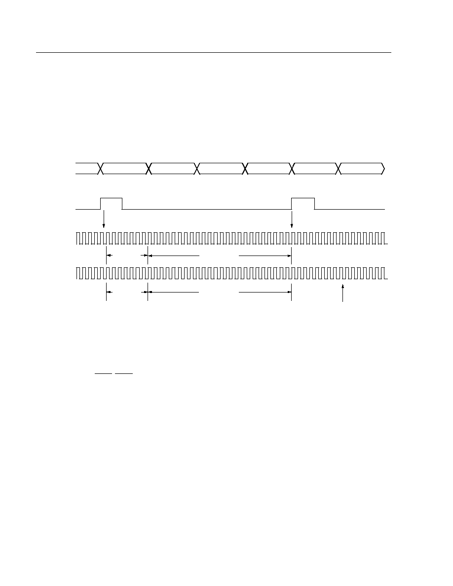
bit times after the beginning of the TDM frame. Figure 5 illustrates using the offsets to configure a system consist-
ing of four time slots, where the initial time slot aligns with the FS. For this system, FE = 0, CLKXI = 1, CLKRI = 0,
TSLT = 000000, and RSLT = 000001.
5-5031
Figure 5. Maximum Bit and Time-Slot Offsets for a Four Time-Slot System
Transmission During Unassigned Time Slots
During time slots when the HIFI-64 is not transmitting, the transmit data output 3-states (an external pull-up resistor
is recommended). This also occurs during masked bit times during a time slot (see the Bit Masking section). If pin
17 is configured to
TSCA
,
TSCA
is high during all time slots other than the assigned time slot and during masked bit
times in the assigned time slot.
Bit Order During Transmission
Data transmission is normally least significant bit (LSB) first per HDLC protocol specifications. In transparent mode,
data is also generated least significant bit first. However, when in the TDM highway mode (HWYEN R0--B7 = 1),
the order of transmission and the expected order for receiving can be reversed by programming the TLBIT and
RLBIT (R10--B6) and (R11--B6), respectively. These bits can be programmed independently of one another. In
other words, the HIFI-64 can be receiving LSB first but transmitting most significant bit (MSB) first, or vice versa.
The effect of TLBIT cleared to 0 is to reverse end-for-end the transmitter-generated data before transmission in the
time slot. All data is reversed, including flags, aborts, CRC, and user data. The effect of RLBIT cleared to 0 is to
reverse end-for-end the time-slot data before passing it to the receiver. RLBIT and TLBIT have no effect on the data
unless HWYEN (R0--B7) = 1.
Figures 6 and 7 show how the transmission and reception of data is affected by adjusting TLBIT and RLBIT. The
convention used represents user data in the FIFO with lower-case letters and HDLC data as upper-case letters.
This convention is meant to indicate only that data in the FIFO and data transmitted or received during the time
slot(s) may not be identical bit-for-bit (i.e., zero-bit insertion and deletion--see the HDLC section of this document).
TS 0
TS 1
TS 2
TS 3
TS 0
TS 1
TDM DATA
FS
CLKX
CLKR
FIRST BIT
RECEIVED
TTSOF = 000011
RTSOF = 000011
TBOF = 111
RBOF = 111
FS LATCHED ON THIS EDGE
FIRST BIT TRANSMITTED
Lucent Technologies Inc.
15
Data Sheet
April 1997
T7121 HDLC Interface for ISDN (HIFI-64)
Functional Description
(continued)
5-5032
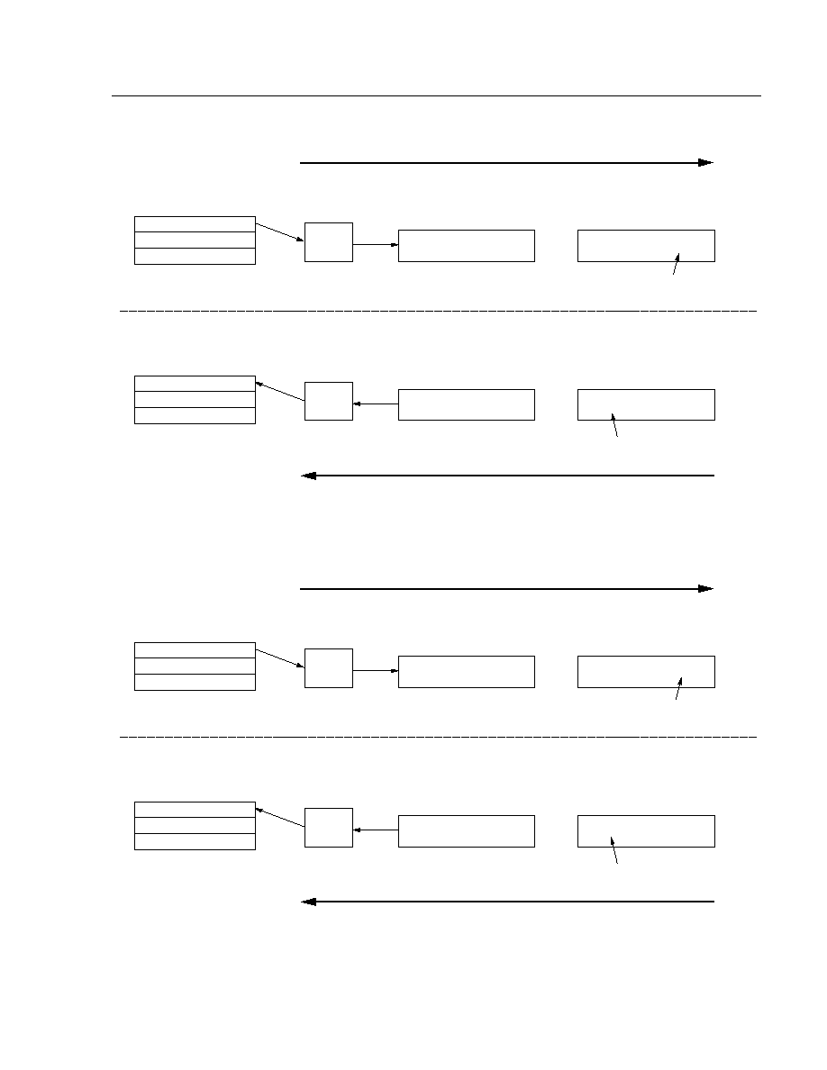
Note: abcdefgh are not the same as ABCDEFGH due to HDLC processing.
Figure 6. Transmission and Reception of Data LSB First
5-5033
Note: abcdefgh are not the same as ABCDEFGH due to HDLC processing.
Figure 7. Transmission and Reception of Data MSB First
a b c d e f g h
HDLC
A B C D E F G H
H G F E D C B A
TRANSMIT FIFO
TRANSMITTER HDLC
PROCESSES LSB FIRST
FIRST BIT
TRANSMITTED
TIME-SLOT DATA
MSB
BIT 7
LSB
BIT 0
MSB
BIT 7
LSB
BIT 0
DIRECTION OF TRANSMISSION
TLBIT = 1 (TRANSMIT LSB FIRST)
a b c d e f g h
HDLC
A B C D E F G H
H G F E D C B A
RECEIVE FIFO
RECEIVER HDLC
EXPECTS LSB FIRST
FIRST BIT
RECEIVED
TIME-SLOT DATA
LSB
BIT 0
MSB
BIT 7
MSB
BIT 7
LSB
BIT 0
DIRECTION OF RECEPTION
RLBIT = 1 (RECEIVE LSB FIRST)
a b c d e f g h
HDLC
A B C D E F G H
H G F E D C B A
TRANSMIT FIFO
TRANSMITTER HDLC
PROCESSES LSB FIRST
FIRST BIT
TRANSMITTED
TIME-SLOT DATA
MSB
BIT 7
LSB
BIT 0
MSB
BIT 7
LSB
BIT 0
DIRECTION OF TRANSMISSION
TLBIT = 0 (TRANSMIT MSB FIRST)
a b c d e f g h
HDLC
A B C D E F G H
H G F E D C B A
RECEIVE FIFO
RECEIVER HDLC
EXPECTS LSB FIRST
FIRST BIT
RECEIVED
TIME-SLOT DATA
LSB
BIT 0
MSB
BIT 7
MSB
BIT 7
LSB
BIT 0
DIRECTION OF RECEPTION
RLBIT = 0 (RECEIVE MSB FIRST)

16
Lucent Technologies Inc.
Data Sheet
April 1997
T7121 HDLC Interface for ISDN (HIFI-64)
Functional Description
(continued)
Bit Masking
When in the TDM highway mode (HWYEN, R0--B7 = 1), the HIFI-64 can be programmed to mask any combina-
tion of bits in a byte. As an example, this feature is used to process 16 kbits/s D-channel data where only 2 bits in
each byte are looked at when receiving, and where only 2 bits are transmitted during an 8-bit time slot. Using this
option, the HIFI-64 is able to support effective intermediate data rates of 8, 16, 24, 32, 40, 48, and 56 kbits/s.
The receiver ignores bit positions that are masked (cleared to 0) in the receiver bit mask register (R12). The trans-
mitter outputs high impedance (3-state) during the bit times specified (cleared to 0) in the transmitter bit mask reg-
ister (R13). The user can program any combination of bits to be masked in the receiver and transmitter
independently.
Upon chip reset, the default is as follows:
1. The receiver defaults to recognize all incoming data as valid (i.e., no masking).
2. The transmitter defaults to a state where all bits are masked.
The user must unmask the bits to be transmitted. This eliminates the problem of the HIFI-64 transmitting before the
time slot has been programmed in registers 7, 9, and 10.
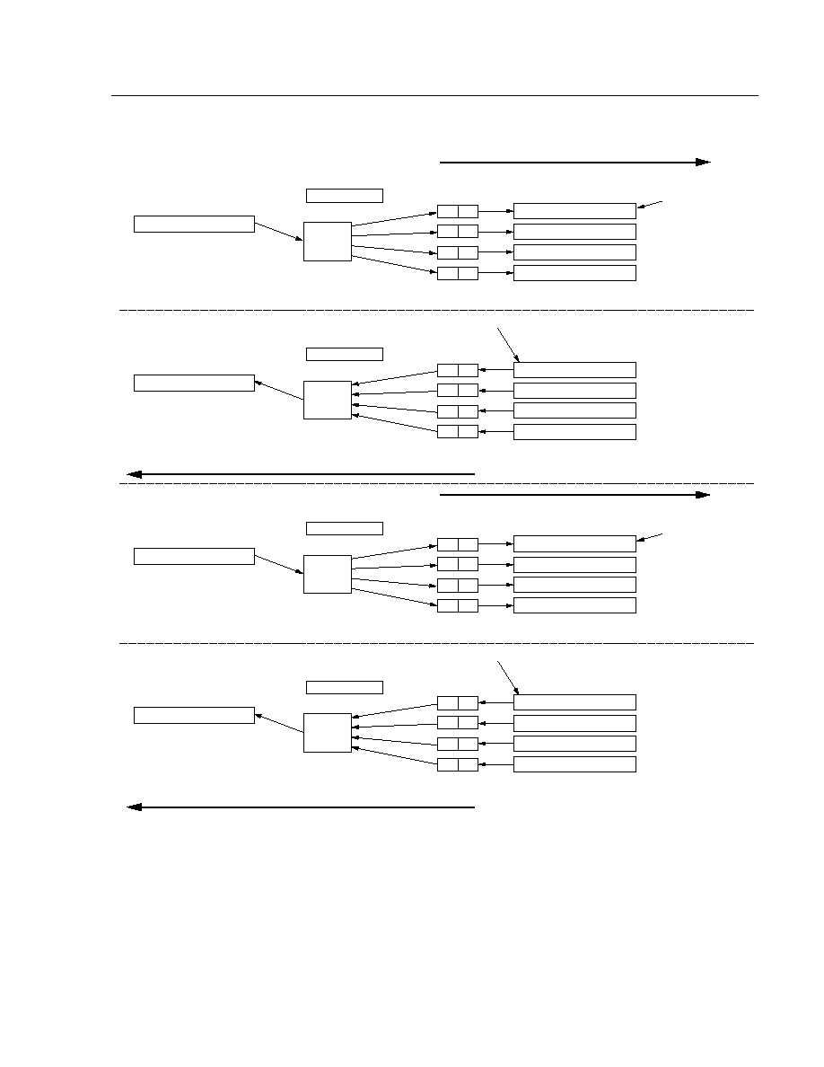
Figures 8 and 9 show how 16 kbits/s operation is achieved by using the bit-masking option.
Lucent Technologies Inc.
17
Data Sheet
April 1997
T7121 HDLC Interface for ISDN (HIFI-64)
Functional Description
(continued)
5-5034
Note: abcdefgh are not the same as ABCDEFGH due to HDLC processing.
Figure 8. 16 kbits/s Operation
a b c d e f g h
HDLC
3 3 3 3 3 3 * G H
TRANSMIT FIFO
TRANSMITTER HDLC
PROCESSES LSB FIRST
FIRST BIT
TRANSMITTED
TIME-SLOT DATA
MSB
BIT 7
LSB
BIT 0
DIRECTION OF TRANSMISSION
TLBIT = 1
(TRANSMIT LSB FIRST)
a b c d e f g h
HDLC
RECEIVE FIFO
RECEIVER HDLC
EXPECTS LSB FIRST
MSB
BIT 7
LSB
BIT 0
DIRECTION OF RECEPTION
TBM7
TBM0
G
H
E
F
C
D
A
B
(R13) TRANSMITTER BIT MASK
3 3 3 3 3 3 E F
3 3 3 3 3 3 C D
3 3 3 3 3 3 A B
*3 = 3-STATE.
1ST TIME SLOT
2ND TIME SLOT
3RD TIME SLOT
4TH TIME SLOT
H G X X X X X X*
FIRST BIT RECEIVED
TIME-SLOT DATA
0 0 0 0 0 0 1 1
RBM7
RBM0
H
G
F
E
D
C
B
A
(R12) RECEIVER BIT MASK
F E X X X X X X
D C X X X X X X
B A X X X X X X
*X = DON'T CARE. THESE BITS
ARE IGNORED BY THE RECEIVER.
1ST TIME SLOT
2ND TIME SLOT
3RD TIME SLOT
4TH TIME SLOT
RLBIT = 1
(RECEIVE LSB FIRST)
a b c d e f g h
HDLC
H G 3 3 3 3 3 3*
TRANSMIT FIFO
TRANSMITTER HDLC
PROCESSES LSB FIRST
FIRST BIT
TRANSMITTED
TIME-SLOT DATA
MSB
BIT 7
LSB
BIT 0
DIRECTION OF TRANSMISSION
TLBIT = 0
(TRANSMIT MSB FIRST)
a b c d e f g h
HDLC
RECEIVE FIFO
RECEIVER HDLC
EXPECTS LSB FIRST
MSB
BIT 7
LSB
BIT 0
DIRECTION OF RECEPTION
TBM7
TBM0
G
H
E
F
C
D
A
B
(R13) TRANSMITTER BIT MASK
F E 3 3 3 3 3 3
D C 3 3 3 3 3 3
B A 3 3 3 3 3 3
*3 = 3-STATE.
1ST TIME SLOT
2ND TIME SLOT
3RD TIME SLOT
4TH TIME SLOT
X*X X X X X G H
FIRST BIT RECEIVED
TIME-SLOT DATA
RBM7
RBM0
H
G
F
E
D
C
B
A
(R12) RECEIVER BIT MASK
X X X X X X E F
X X X X X X C D
X X X X X X A B
1ST TIME SLOT
2ND TIME SLOT
3RD TIME SLOT
4TH TIME SLOT
RLBIT = 0
(RECEIVE MSB FIRST)
0 0 0 0 0 0 1 1
0 0 0 0 0 0 1 1
0 0 0 0 0 0 1 1
*X = DON'T CARE. THESE BITS
ARE IGNORED BY THE RECEIVER.
18
Lucent Technologies Inc.
Data Sheet
April 1997
T7121 HDLC Interface for ISDN (HIFI-64)
Functional Description
(continued)
5-5035
Note: abcdefgh are not the same as ABCDEFGH due to HDLC processing.
Figure 9. 16 kbits/s Operation, MSB First
a b c d e f g h
HDLC
3 3 3 3 3 3* H G
TRANSMIT FIFO
TRANSMITTER HDLC
PROCESSES LSB FIRST
FIRST BIT
TRANSMITTED
TIME-SLOT DATA
MSB
BIT 7
LSB
BIT 0
DIRECTION OF TRANSMISSION
TLBIT = 0
(TRANSMIT MSB FIRST)
a b c d e f g h
HDLC
RECEIVE FIFO
RECEIVER HDLC
EXPECTS LSB FIRST
MSB
BIT 7
LSB
BIT 0
DIRECTION OF RECEPTION
11000000
TBM7
TBM0
G
H
E
F
C
D
A
B
(R13) TRANSMITTER BIT MASK
3 3 3 3 3 3 F E
3 3 3 3 3 3 D C
3 3 3 3 3 3 B A
*3 = 3-STATE.
1ST TIME SLOT
2ND TIME SLOT
3RD TIME SLOT
4TH TIME SLOT
G H X X X X X X*
FIRST BIT RECEIVED
TIME-SLOT DATA
11000000
RBM7
RBM0
H
G
F
E
D
C
B
A
(R12) RECEIVER BIT MASK
E F X X X X X X
C D X X X X X X
A B X X X X X X
*X = DON'T CARE. THESE BITS
ARE IGNORED BY THE RECEIVER.
1ST TIME SLOT
2ND TIME SLOT
3RD TIME SLOT
4TH TIME SLOT
RLBIT = 0
(RECEIVE MSB FIRST)

Lucent Technologies Inc.
19
Data Sheet
April 1997
T7121 HDLC Interface for ISDN (HIFI-64)
Functional Description
(continued)
SLD and IOM2 Examples
Example register settings for configuring to SLD, IOM2, or K2 TDM highways are shown below. These settings
assume HWYEN (R0--B7) = 1 and FSPOL (R0--B6) = 1.
HDLC Operation
This section describes the standard HDLC functions performed by the HIFI-64. HDLC operation is the default
mode of operation. The transmitter accepts parallel data from the transmit FIFO, converts it to a serial bit stream,
provides bit stuffing as necessary, adds the CRC and the opening and closing flags, and sends the framed serial
bit stream on the selected transmit data pin(s). The receiver accepts serial data on the selected receive data pin,
identifies frames for proper format, reconstructs data bytes, provides bit destuffing as necessary, and loads parallel
data in the receive FIFO. HDLC frames on the serial link have the following format:
All bits between the opening flag and the CRC are considered user data bits. User data bits such as the address,
control, and information fields for LAPB or LAPD frames are fetched from the transmit FIFO for transmission.
Received user data bits are stored in the FIFO buffers. The 16 bits preceding the closing flag are the frame check
sequence or cyclic redundancy check (CRC) bits.
Zero-Bit Insertion/Deletion (Bit Stuffing/Destuffing)
The HDLC protocol recognizes three special bit patterns: flags, aborts, and idles. These patterns have the com-
mon characteristic of containing at least six consecutive 1s. A user data byte can contain one of these special pat-
terns. Transmitter zero-bit stuffing is done on user data and CRC fields of the frame to avoid transmitting one of
these special patterns. Whenever five 1s occur between flags, a 0 bit is automatically inserted after the fifth 1, prior
to transmission of the next bit. On the receive side, if five successive 1s are detected followed by a 0, the 0 is
assumed to have been inserted and is deleted (bit destuffing).
Table 4. Example Register Settings
Register
IOM2/GCI
SLD
K2
FE, (R0--B5)
0
0
0
P21CTL, (R5--B6)
1
1
1
CMS, (R8--B6)
1
0
0
CLKXI, (R9--B4)
1
1
1
TBOF[2--0], (R9--B[7--5])
111
111
111
TTSOF[5 0], (R10--B[5--0])
(# of time slots) ≠ 1
000011
000000, 000111
TSLT[5--0], (R7--B[5--0])
Desired time slot
000000--000011
000001--000111, 000000
CLKRI, (R9--B0)
0
0
0
RBOF[2--0], (R9--B[3--1])
111
111
111
RTSOF[5--0], (R11--B[5--0])
(# of time slots) ≠ 1
000011
000000, 000111
RSLT[5--0], (R8--B[5--0])
Desired time slot
000100--000111
000001--000111, 000000
Opening Flag
User Data Field
Frame Check Sequence (CRC)
Closing Flag
01111110
8 bits
16 bits
01111110

20
20
Lucent Technologies Inc.
Data Sheet
April 1997
T7121 HDLC Interface for ISDN (HIFI-64)
Functional Description
(continued)
Flags. All flags have the bit pattern 01111110 and are
used for frame synchronization. The HIFI-64 automati-
cally sends two flags between frames. If the FLAGS bit
in the chip-configuration register (R0--B2) is cleared to
0, the 1s idle byte (11111111) is sent between frames if
no data is present in the FIFO. Once there is data in the
transmit FIFO, an opening flag is sent followed by the
frame. If the FLAGS bit (R0--B2) is set to 1, the HIFI-
64 sends continuous flags when the transmit FIFO is
empty. During transmission, two successive flags will
not share the intermediate 0. The HIFI-64 does not
transmit consecutive frames with a shared flag.
An opening flag is generated at the beginning of a
frame (indicated by the presence of data in the transmit
FIFO and the transmitter enabled). Data is transmitted
per the HDLC protocol until a byte is read from the
FIFO with TFC set. The HIFI-64 follows this byte with
the CRC sequence and a closing flag.
The receiver recognizes the 01111110 pattern as a
flag. Two successive flags may or may not share the
intermediate 0 bit and are identified as two flags (i.e.,
both 011111101111110 and 0111111001111110 are
recognized by the HIFI-64). The received data bytes
are stored in the 64-byte receive FIFO delayed by three
bytes or delayed by four bytes if operating in the TDM
highway mode (i.e., HWYEN, R0--B7 = 1). When
another flag is identified, it is treated as the closing flag.
As mentioned above, a flag sequence in the user data
or FCS fields is prevented by zero-bit insertion and
deletion. The received CRC bytes are not loaded into
the receive FIFO. The HIFI-64 receiver recognizes a
single flag between frames as both a closing and open-
ing flag.
Aborts. The bit pattern of the abort sequence is
01111111, with 0 transmitted first. A frame can be
aborted by writing a 1 to TABT (R1--B6). This causes
the last byte written to the transmit FIFO to be replaced
with the abort sequence upon transmission. Once a
byte is tagged by a write to TABT, it cannot be cleared
by subsequent writes to R1. TABT (R1--B6) and TFC
(R1--B7) should never be set to 1 simultaneously
since this causes the transmitter to enter an invalid
state that requires a transmitter reset to clear. A frame
should not be aborted in the very first byte following the
opening flag. An easy way to avoid this situation is to
first write a dummy or junk byte into the queue and then
write the abort command to the queue.
When receiving a frame, the receiver recognizes the
abort sequence whenever it receives a 0 followed by
seven consecutive 1s. This status results in the abort
bit, and possibly the bad byte count bit and/or bad CRC
bits, being set in the Status of Frame status byte which
is appended to the receive data queue. The last two
bytes of user data are assumed to be CRC bits and are
not placed in the queue. All subsequent bytes are
ignored until a valid opening flag is received.
Idles. In accordance with the HDLC protocol, the HIFI-
64 recognizes 15 or more contiguous received 1s as
idle. When the HIFI-64 receives 15 contiguous 1s, the
receiver idle bit (RIDL, R15--B6) is set in register 15.
An interrupt pin transition is generated if no other
unmasked interrupts are active and the RIDL interrupt
is unmasked; i.e., RIIE (R14--B6) = 1.
For transmission, the 1s idle byte is defined as the
binary pattern 11111111 (FF hexadecimal). If the
FLAGS control bit in the chip configuration register
(R0--B2) is 0, the 1s idle byte is sent as the time-fill
byte between frames. A time-fill byte is sent when the
transmit FIFO is empty and the transmitter has com-
pleted transmission of all previous frames. Frames are
sent back-to-back otherwise. If the FLAGS bit (R0--B2)
is set to 1, flags (01111110) are sent as the time-fill
byte between frames. 1s idle is the default time-fill byte.
Note: Regardless of the time-fill byte used, there
always is an opening and closing flag with each
frame. Back-to-back frames are separated by
two flags.
CRC. For a given frame of bits, 16 additional bits that
constitute an error-detecting code are added by the
transmitter. As called for in the HDLC protocol, the
Frame Check Sequence bits are transmitted most sig-
nificant bit first and are bit stuffed. The Cyclic Redun-
dancy Check (or Frame Check Sequence) is calculated
as a function of the transmitted bits by using the ITU-T
standard polynomial:
x
16
+ x
12
+ x
5
+ 1
At the other end, the receiver performs the same calcu-
lation on the received bits after destuffing and com-
pares the results to an expected result. An error occurs
if, and only if, there is a mismatch.
The transmitter can be instructed to transmit a cor-
rupted CRC by setting the Transmit Bad CRC bit
TBCRC (R14--B7). As long as the TBCRC bit is set,
the CRC is corrupted for each frame transmitted by log-
ically flipping the least significant bit of the transmitted
CRC.
The receiver calculates and verifies the CRC for an
incoming frame. The result of the CRC check is
reported in bit 7 of the Status of Frame byte which is
placed in the receive FIFO after the last data byte of
the frame. The CRC is not stored in the FIFO.

Lucent Technologies Inc.
21
Data Sheet
April 1997
T7121 HDLC Interface for ISDN (HIFI-64)
Functional Description
(continued)
Transmitter FIFO
Data associated with multiple frames can be written to
the transmit FIFO by the controlling microprocessor.
However, all frames must be explicitly tagged with a
Transmit Frame Complete (TFC) bit (R1--B7) or a
Transmit Abort (TABT) bit (R1--B6) by writing to regis-
ter 1. The TFC is tagged onto the last byte of a frame
written into the transmitter FIFO. TFC instructs the
transmitter to end the frame by attaching the CRC and
closing flag following the tagged byte. Once written, the
TFC cannot be changed by another write to R1. If TFC
is not written before the last data byte is read out for
transmission, an underrun occurs. When the FIFO is
empty, writing two data bytes to the FIFO before setting
TFC provides a minimum of eight CLKX periods to
write TFC. TABT (R1--B6) and TFC (R1--B7) should
never be set to 1 simultaneously. This causes the trans-
mitter to enter an invalid state requiring a transmitter
reset.
When the transmitter has completed a frame, with a
closing flag or an abort sequence, the TDONE
(R15--B0) bit is set to 1. If TDIE (R14--B0) is 1 and no
other prior unacknowledged interrupt exists, the INT
pin transitions.
Sending 1-Byte Frames
Sending 1-byte frames with an empty transmit FIFO is
not recommended. If the FIFO is empty, writing two
data bytes to the FIFO before setting TFC provides a
minimum of eight CLKX periods to write TFC. When
one byte is written to the FIFO, TFC must be written
within 1 CLKX period to guarantee it is effective. Thus,
1-byte frames are subject to underrun aborts. One-byte
frames cannot be aborted with TABT. Placing the trans-
mitter in 1s idle mode (FLAGS, R0--B2 = 0) lessens
the frequency of underruns. If the transmit FIFO is not
empty, then 1-byte frames present no problem.
Transmitter Underrun
After writing a byte to the transmit queue, the user has
eight CLKX cycles in which to write the next byte before
a transmitter underrun occurs. An underrun occurs
when the transmitter has finished transmitting all the
bytes in the queue, but the frame has not yet been
closed by writing TFC. When a transmitter underrun
occurs, the abort sequence is sent at the end of the last
valid byte transmitted. A TDONE interrupt is generated,
and the transmitter reports an underrun abort in the
interrupt status register (R15--B2). The transmitter
enters forced idle (sending FLAGS or IDLES based
upon the value in R0--B2) until the interrupt status reg-
ister (R15) is read.
Using the Transmitter Status and Fill Level
The Transmitter-interrupt Level bits (R1--B[5--0]) allow
the user to instruct the T7121 to interrupt the host pro-
cessor whenever the transmitter has a predetermined
number of empty locations. The number of locations
selected determines the time between transmitter
empty (TE) interrupts. The transmitter status bits
(R2--B[6--0]) report the number of empty locations in
the transmitter FIFO. The bits are encoded in binary
with bit 0 the least significant bit. Also found in register
2 is the Transmitter Empty Dynamic bit, TED (R2--B7).
This bit, like the TE interrupt bit, is set when the number
of empty locations is less than or equal to the pro-
grammed empty level. TED returns to 0 when the trans-
mitter is filled to above the programmed empty level.
Polled interrupt systems can use TED to determine
when they can write to the transmit FIFO.
Programming Note: After the transmitter is turned off,
a transmitter reset should be performed (TRES, R6, bit
5 = 1) before the transmitter is turned on. After the
receiver is turned off, a receiver reset should be per-
formed (RRES, R6, bit 4 = 1) before the receiver is
turned on. The transmitter and receiver should both be
reset individually (i.e., not at the same time) after any
concentration highway configuration change. If TRES =
RRES = 1 at the same time, a full chip reset is per-
formed: all register bits are forced to their reset values.
Receiver FIFO
The receiver status is available in two ways. First, the
queue manager creates a Status of Frame (SF) byte for
each HDLC frame and stores this status byte in the
FIFO after the last data byte of the associated frame.
Thus, a frame containing 24 user data bytes results in
25 bytes present in the receive FIFO. The SF status
byte has the following format:
STATUS OF FRAME BYTE
BIT7
BIT6
BIT5
BIT4
BIT3
BIT2
BIT1
BIT0
BAD CRC
ABOR
T
O
VERR
UN
BAD BYTE COUNT
0
0
0
0

22
22
Lucent Technologies Inc.
Data Sheet
April 1997
T7121 HDLC Interface for ISDN (HIFI-64)
Functional Description
(continued)
Bit 7 of the SF status byte is the CRC status bit. If an
incorrect CRC was detected, this bit is set to 1. If the
CRC was correct, the bit is 0.
Bit 6 of the SF status byte is the abort status. A high (1)
indicates the frame associated with this status byte was
aborted (i.e., the abort sequence was detected after an
opening flag and before a subsequent closing flag). An
abort can also cause bits 7 and/or 4 to go high (1). An
abort is not reported when a flag is followed by seven
1s.
If the Overrun bit (bit 5) is high, it indicates that a
receiver FIFO overrun occurred (the 64-byte FIFO size
was exceeded; see the Receiver Overrun section).
The Bad Byte Count bit (Bit 4) indicates whether or not
the bit count received was a multiple of eight (i.e., an
integer number of bytes). A high (1) indicates that the
bit count received after 0-bit deletion was not a multiple
of eight, and a low indicates that the bit count was a
multiple of eight. When a non-byte-aligned frame is
received, all bits received are present in the receive
FIFO. The byte before the SF status byte contains less
than eight valid data bits. The nondata bits are the first
bits of the received CRC. The T7121 provides no indi-
cation of how many of the bits in the byte are valid. It is
up to the user and the protocol to decide what to do
with non-byte-aligned frames.
Bits 0 to 3 of the SF status byte are not used and are
guaranteed to be 0 when read. A good frame is implied
when the SF status byte is 00 hexadecimal.
The last byte of a completed frame in the receive FIFO
is always the SF status byte. As a frame is received,
the two bytes preceding the closing flag are assumed
to be the frame check sequence (CRC) bits and are not
loaded into the receiver FIFO. Thus, the final 2 bytes
received in an aborted frame are not placed in the
queue, and an aborted frame of 2 bytes or less causes
only an SF status byte to appear in the receiver FIFO.
The writing of the SF status byte is followed by the
REOF (R15--B4) interrupt bit being set. The REOF
event triggers an interrupt, unless the interrupt is
masked by REOFIE (R14--B4) = 0, whenever no other
unmasked interrupts are active.
The Receive Queue Status bits (RQS, R4--[6--0]) are
updated as bytes are loaded into the receive FIFO. The
SF status byte is included in the byte count. When the
first SF status byte is placed in the FIFO, the EOF
(R4--B7) bit is set, and the status freezes until the
FIFO is read. As bytes are read from the FIFO, the sta-
tus decreases until it reads 1. The byte read when the
RQS is "0000001" and the EOF bit is high (1) is the SF
status byte describing the error status of the frame just
read. Once the first SF status byte is read from the
FIFO, the FIFO status is updated to report the number
of bytes to the next SF status byte, if any, or the number
of additional bytes present. When EOF (R4--B7) is
low, no SF status byte is currently present in the FIFO,
and the RQS bits report the number of bytes present.
As bytes are read from the FIFO, the status decreases
with each read until it reads 0 when the FIFO is totally
empty. The EOF bit is also low when the FIFO is com-
pletely empty. Thus, the RQS and EOF bits provide a
mechanism to recognize the end of one frame and the
beginning of another. Reading the receiver status reg-
ister (R4) does not affect the FIFO buffers. In the event
of a receiver overrun (see below), an SF status byte is
written to the receive FIFO. Multiple SF status bytes
can be present in the FIFO. Remember, the RQS
reports only the number of bytes to the first SF status
byte.
To allow users to tailor receiver FIFO service intervals
to their systems, the Receiver Interrupt Level bits
(RIL, R5--B[5--0]) are provided. These bits are coded
in binary and determine when the Receiver Full
(RF, R15--B3) interrupt is asserted. The interrupt pin
transition can be masked by clearing RFIE, R14--B3 to
0. The value programmed in the RIL bits equals the
total number of bytes necessary to be present in the
FIFO to trigger an RF interrupt. The RF interrupt alone
is not sufficient to determine the number of bytes to
read as some of the bytes may be SF status bytes. The
RQS bits and EOF bit in register 4 allow the user to
determine the number of bytes to read. The REOF
interrupt can be the only interrupt for the final frame of
a group of frames, since the number of bytes received
to the end of the frame cannot be sufficient to trigger an
RF interrupt.

Lucent Technologies Inc.
23
Data Sheet
April 1997
T7121 HDLC Interface for ISDN (HIFI-64)
Functional Description
(continued)
Programming Note: Since the receiver writing to the
receive FIFO and the host reading from the receive
FIFO are asynchronous events, it is possible for a host
read to put the number of bytes in the receive FIFO just
below the programmed RIL level and a receiver write to
put it back above the RIL level. This causes a new RF
interrupt. This has the potential to cause software prob-
lems. It is recommended that during service of the RF
interrupt, the RF interrupt be masked RFIE (R14--B3)
= 0 and the interrupt register be read at the end of the
service routine, discarding any RF interrupt seen,
before unmasking the RF interrupt.
Programming Note: After the transmitter is turned off,
a transmitter reset should be performed (TRES, R6, bit
5 = 1) before the transmitter is turned on. After the
receiver is turned off, a receiver reset should be per-
formed (RRES, R6, bit 4 = 1) before the receiver is
turned on. The transmitter and receiver should both be
reset individually (i.e., not at the same time) after any
concentration highway configuration change. If TRES =
RRES = 1 at the same time, a full chip reset is per-
formed: all register bits are forced to their reset values.
Receiver Overrun
A receiver overrun occurs if the 64-byte limit of the
receiver FIFO is exceeded, i.e., data has been received
faster than it has been read out of the receive FIFO and
written to the system memory. Upon overrun, an SF
status byte with the overrun bit (bit 5) set replaces the
last byte in the FIFO. The SF status byte can have
other error conditions present. For example, it is
unlikely the CRC is correct. Thus, care should be taken
to prioritize the possible frame errors in the software
service routine. The last byte in the FIFO is overwritten
with the SF status byte regardless of the type of byte
(data or SF status) being overwritten. The overrun con-
dition is reported in register 15 (R15--B5) and causes
the interrupt pin to be asserted if it is not currently
asserted and it is not masked (ROVIE, R14--B5). Data
is ignored until the condition is cleared. The overrun
condition is cleared by reading register 15 and reading
at least 1 byte from the receive FIFO. Because multiple
frames can be present in the FIFO, good frames as
well as the overrun frame can be present. The host can
determine the overrun frame by looking at the SF sta-
tus byte.
Operational Note (T7121-EL, T7121-PL, T7121-EL2,
and T7121-PL2)
In HDLC protocol, binary 1s may be transmitted
between frames (interframe fill) when no user data is
available. Short bursts of interframe fill, not specified in
the current standards, have been encountered when
system testing against some switch equipment. Per
Lucent's interpretation of the standards, the device will
treat received interframe fill from 1 bit to 5 bits in length
as a short packet and report a received end of frame
condition in register R15, bit 4 (EOF = 1). A hardware
interrupt will be generated if the REOF interrupt is
enabled in register R14, bit 4 (REOFIE = 1). This may
be a performance issue in some systems due to the
extra interrupts that the host processor must service,
produced by short bursts of interframe fill from 1 bit to
5 bits in length.
The contents of both register R4 (Receiver Status Reg-
ister) and the receive FIFO depend on the number of
interframe 1s received.
If one bit of interframe fill is received, R4 will indicate
that an end of frame has occurred, but zero bytes are
stored in the receive FIFO (i.e., no Status of Frame
byte was written to the FIFO). Data reception can pro-
ceed normally without further intervention by the host
processor.
If 2 bits to 5 bits of interframe fill are received, R4 will
indicate that an end of frame has occurred, and that
one byte was stored in the receive FIFO. The 1 byte
stored in the FIFO is the Status of Frame byte due to
the interframe fill and will have a value of 0x90, indicat-
ing a bad CRC and bad byte count. This byte should be
read out and discarded. After removing the Status of
Frame byte from the FIFO, data reception can proceed
normally without further intervention by the host micro-
processor.
If 6 bits or more of interframe fill are received, the
device correctly ignores these bits. The FIFO is not
written and no interrupts are generated.

24
24
Lucent Technologies Inc.
Data Sheet
April 1997
T7121 HDLC Interface for ISDN (HIFI-64)
Functional Description
(continued)
Transparent Mode
The HIFI-64 can be programmed to operate in the
transparent mode by setting the TRANS bit
(AR11--B6) to 1. In the transparent mode of operation,
no HDLC processing is performed on user data. The
transparent mode can be exited at any time by clearing
the TRANS bit to 0. It is recommended that the trans-
mitter be disabled (ENT, R6--B3 = 0) when changing in
and out of transparent mode. The transmitter should be
reset by a TRES whenever the mode is changed.
Three alternate registers are provided to control opera-
tion in the transparent mode:
AR11--Transparent Mode Control
AR12--Receive Match Character
AR13--Transmitter Idle Character
The alternate registers are accessed by setting the ALT
bit (R0--B4) to 1. All subsequent addressing of regis-
ters 11 through 13 then refer to the alternate registers
(AR11--AR13). Returning to the foreground register
set is accomplished by clearing the ALT bit (R0--B4) to
0.
In the transmit direction, the HIFI-64 takes data from
the transmit FIFO and transmits that data exactly bit for
bit on the DXA pin, the DXB pin, or both, depending on
the configuration of the DXAC and DXBC bits in regis-
ter 7 (R7--B6, B7). When there is no data in the trans-
mit FIFO, the HIFI-64 either transmits all 1s, or
transmits the transmitter idle character programmed in
AR13 if the MATCH bit (AR11--B5) is set to 1. To
cause the transmit idle character to be sent first, the
character must be programmed in AR13 before the
transmitter is enabled. In non-TDM highway modes,
the transmit idle character or the 1s idle character
is always sent first, even if data is present in the
FIFO. In TDM highway mode, the first character trans-
mitted is FF hexadecimal regardless of the mode. The
bits are transmitted least significant bit first in non-TDM
highway mode (HWYEN, R0--B7 = 0). In TDM highway
modes (HWYEN = 1), the TLBIT (R10--B6) deter-
mines the bit transmission order. Subrate operation
using the transmit bit mask is also supported. The
transmitter empty (TE) interrupt acts normal.
The transmitter-done interrupt (TDONE) is used to
report an empty transmit FIFO. The TDONE interrupt
thus provides a way to determine transmission end. In
transparent mode, a TDONE interrupt is generated
when the transmitter is reset, as does a TE interrupt.
The UNDABT interrupt is not active in transparent
mode.
If the HIFI-64 is in the TDM highway mode (HWYEN,
R0--B7 = 1), transmit data is octet-aligned to the
selected time slot. If HWYEN = 0, transmit data is
octet-aligned to the first CLKX after the transmitter has
been enabled (ENT, R6 B3 = 1). See Figure 3 for
details of clock start-up in non-TDM highway modes.
In the receive direction, the HIFI-64 loads received data
from the DRA or DRB pin (depending on the configura-
tion of the DRA/B bit in register 8 [R8--B7]) directly into
the receive FIFO bit for bit. In non-TDM highway
modes, the data is assumed to be least significant bit
first. In TDM highway mode, the RLBIT (R11 B6) con-
trols the bit order. If the MATCH bit (AR11--B5) is 0,
the receiver begins loading data into the receive FIFO,
beginning with the first CLKR detected after the
receiver has been enabled (ENR, R6--B2 = 1). If the
MATCH bit (AR11--B5) is set to 1, the receiver does
not begin loading data into the FIFO until the receiver
match character programmed in AR12 has been
detected. The search for the receiver match character
is in a sliding window fashion if the ALOCT (Align to
Octet) bit (AR11--B4) is 0, or only on octet boundaries
if the ALOCT bit is set to 1. The octet boundary is
aligned to the receive time slot if HWYEN (R0--B7) = 1
or relative to the first CLKR after the receiver has been
enabled (ENR, R6--B2 = 1), if HWYEN (R0--B7) = 0.
The matched character and all subsequent bytes are
placed in the receive FIFO. A receiver reset RRES
causes the receiver to realign to the match character if
MATCH is set.
The receiver full (RF) and receiver overrun (OVERUN)
interrupts act as normal. The received end of frame
(REOF) and receiver idle (RIDL) interrupts are not
used in the transparent mode. The match status
(MSTAT) bit (AR11--B4) is set to 1 when the receiver
match character is first recognized. If the MATCH bit
(AR11--B5) is 0, the MSTAT bit (AR11--B4) is set to 1
automatically when the first bit is received, and the
octet offset status bits (AR11--B[0--2]) read 000. If the
MATCH bit (AR11--B5) is programmed to 1, the
MSTAT bit (AR11--B4) is set to 1 upon recognition of
the first receiver match character, and the octet offset
status bits (AR11--B[0--2]) indicate the offset relative
to the octet boundary at which the receiver match char-
acter was recognized. The octet offset status bits have
no meaning until the MSTAT bit is set to 1. An octet off-
set of 111 indicates byte alignment.
An interrupt for recognition of the match character can
be generated by setting the RIL level to 1. Since the
matched character is the first byte written to the FIFO,
the RF interrupt occurs with the writing of the match
character to the receive FIFO.

Lucent Technologies Inc.
25
Data Sheet
April 1997
T7121 HDLC Interface for ISDN (HIFI-64)
Functional Description
(continued)
Programming Note: The match bit (MATCH) affects both the transmitter and the receiver. Care should be taken to
correctly program both the transmit idle character and the receive match character before setting MATCH. If the
transmit idle character is programmed to FF hex, the MATCH bit appears to affect only the receiver.
The operation of the receiver in transparent mode is summarized in Table 5.
Diagnostic Modes
Loopbacks
The serial link interface can operate in two diagnostic loopback modes: (1) local loopback and (2) remote loopback.
The local loopback mode is selected when the LLOOP bit is set to 1 in the operation control register (R6--B1). The
remote loopback is selected when the RLOOP bit is set to 1 in the operation control register (R6--B0). For normal
traffic, i.e., to operate the transmitter and receiver independently, the LLOOP bit and the RLOOP bit should both be
cleared to 0. Loopbacks are available in both TDM highway and non-TDM highway modes. Do not simultaneously
attempt local and remote loopbacks.
Either DRA or DRB can be used for receive data, based on the value of the DRA/B bit in register 8 (R8--B7). DXA
or DXB or both can be selected for transmit data, depending on the values programmed for the DXAC and DXBC
bits in register 7 (R7--B6 and R7--B7).
Table 5. Receiver Operation in Transparent Mode
HWYEN
(R0--B7)
ALOCT
(AR11--B4)
MATCH
(AR11--B5)
Receiver Operation
0
X
0
Serial-to-parallel conversion begins with first CLKR after
ENR is set. Data loaded to receive FIFO immediately.
0
0
1
Match user-defined character (AR12) using sliding window.
Byte aligns once character is recognized. No data to
receive FIFO until match is detected.
0
1
1
Match user-defined character (AR12), but only on octet
boundary. Boundary based on first CLKR after ENR set. No
data to receive FIFO until match is detected.
1
X
0
Byte aligns to time slot. No match necessary. Data loaded
to receive FIFO immediately.
1
0
1
Match user-defined character (AR12) using sliding window.
Byte aligns once character is recognized. No data to
receive FIFO until match is detected.
1
1
1
Match user-defined character (AR12) to byte received in
time slot. No data to receive FIFO until match is detected.
26
Lucent Technologies Inc.
Data Sheet
April 1997
T7121 HDLC Interface for ISDN (HIFI-64)
Functional Description
(continued)
In the local loopback mode:
s
CLKRI (R9--B0) must equal CLKXI (R9--B4). We recommend changing CLKRI to match CLKXI (other highway
parameters need not be altered).
s
CLKX clocks both the transmitter and the receiver.
s
The transmitter and receiver must both be enabled. The transmitter output is internally connected to the receiver
input.
s
The DXA and DXB outputs are active, depending on DXAC and DXBC.
s
The DRA or DRB input is ignored.
s
The communication between the transmit and receive FIFO buffers and the microprocessor continues normally.
5-5036
Figure 10. Local Loopback Mode
HDLC
CHI
DATA TO BE
TRANSMITTED
TRANSMITTER
DXA
DXB
(USER-SELECTED)
FIFO
HDLC
CHI
DRA
DRB
(IGNORED)
FIFO
OR
RECEIVER
Lucent Technologies Inc.
27
Data Sheet
April 1997
T7121 HDLC Interface for ISDN (HIFI-64)
Functional Description
(continued)
In the remote loopback mode:
CLKR must equal or be synchronous with CLKX. We recommend clocking both transmit and receive data with
CLKX (R5--B6 set to 1).
s
Receive and transmit bit masks (R12 and R13) should be programmed to the same value.
s
Transmitted data is retimed. If HWYEN = 0 (R0--B7), the transmitted data is retimed with a maximum delay of
2 bits. If HWYEN = 1 (R0--B7), the received data is transmitted in the first programmed time slot after the
receive time slot is complete.
s
Received data is retransmitted on the DXA and/or the DXB output, depending on DXAC and DXBC.
s
The transmitter should be disabled. The receiver can be disabled or, if desired, enabled. Received data is sent
as usual to the receive FIFO if the receiver is enabled.
5-5037
Figure 11. Remote Loopback Mode
CAUTION: Do not use local and remote loopback modes at the same time. Such use results in an
unknown state in the chip which only a full reset of the chip can clear.
HDLC
CHI
TRANSMITTER
DXA
DXB
(USER-SELECTED)
FIFO
HDLC
CHI
FIFO
RECEIVER
DRA
OR
DRB
(USER-SELECTED)

28
Lucent Technologies Inc.
Data Sheet
April 1997
T7121 HDLC Interface for ISDN (HIFI-64)
Functional Description
(continued)
3-State Mode
The HIFI-64 can be placed in a high-impedance mode for test purposes. In this configuration, all output pins are
placed in a 3-state condition. This can be accomplished in two different ways:
1. Asserting the RESET pin 3-states all outputs, clears both the transmit and receive FIFOs, and resets all internal
registers to their default values. A full chip reset occurs with or without a clock input.
2. Setting the 3STATE bit (R6--B6) to 1 3-states all outputs without affecting the states of internal registers and
FIFOs. This state lasts until both
CS
and
RD
are held low; that is, the first read of the HIFI-64 resets the 3STATE
bit regardless of the register address. Registers can be written while the 3STATE bit is enabled.
Setting the receiver reset (RRES) and the transmitter reset (TRES) bits in the operation control register
(R6--B4,B5) to 1 simultaneously causes a FIFO and register reset to reset values (outputs are not 3-stated).
Other
The HIFI-64 can be instructed to transmit a bad CRC for test purposes by programming the TBCRC bit in register
14 (R14--B7) to 1. Bad CRCs are transmitted until the TBCRC bit is cleared. The TEST bit in AR11 is used for
manufacture testing and should always be programmed low (0) by the host microprocessor.
Powerdown Mode
The HIFI-64 can be placed in a low-power mode when not in use by setting the PDWN bit in register 6 (R6--B7) to
1. This has the effect of stopping data clock input signals (CLKR and CLKX) from propagating internally and results
in very low power dissipation. Reads and writes to the HIFI-64 can continue normally. The low-power mode is
exited by clearing the PDWN bit (R6--B7) to 0.
Registers
The HIFI-64 contains 19 registers (R0--R15 and AR11--AR13). Registers 11, 12, and 13 have alternate meanings
depending on the value of the ALT bit in the Chip Configuration Register (R0--B4). The alternate registers are
accessed by setting the ALT bit (R0--B4) to 1. All subsequent addressing of registers 11 through 13 then refers to
the alternate registers (AR11--AR13). Returning to the foreground register set is accomplished by clearing the ALT
bit (R0--B4) to 0. The primary function of the alternate registers is for transparent-mode operation.
A summary of the HIFI-64 register set is given in Table 6.
Lucent Technologies Inc.
29
Data Sheet
April 1997
T7121 HDLC Interface for ISDN (HIFI-64)
Functional Description
(continued)
Table 6. HIFI-64 Register Summary
Reg#
R/W
Bit 7
Bit 6
Bit 5
Bit 4
Bit 3
Bit 2
Bit 1
Bit 0
Chip Configuration
R0
R/W
HWYEN
FSPOL
FE
ALT
BM
FLAGS
IPOL
DINT
Transmitter Control
R1
R/W
TFC
TABT
TIL5
TIL4
TIL3
TIL2
TIL1
TIL0
Transmitter Status
R2
R
TED
TQS6
TQS5
TQS4
TQS3
TQS2
TQS1
TQS0
Data Byte
R3
R/W
DATA7
DATA6
DATA5
DATA4
DATA3
DATA2
DATA1
DATA0
Receiver Status
R4
R
EOF
RQS6
RQS5
RQS4
RQS3
RQS2
RQS1
RQS0
Receiver Control
R5
R/W
P17CTL
P21CTL
RIL5
RIL4
RIL3
RIL2
RIL1
RIL0
Operation Control
R6
R/W
PDWN
3STATE
TRES
RRES
ENT
ENR
LLOOP
RLOOP
Transmit Time-Slot Control
R7
R/W
DXAC
DXBC
TSLT5
TSLT4
TSLT3
TSLT2
TSLT1
TSLT0
Receiver Time-Slot Control
R8
R/W
DRA/B
CMS
RSLT5
RSLT4
RSLT3
RSLT2
RSLT1
RSLT0
Bit Offset Control
R9
R/W
TBOF2
TBOF1
TBOF0
CLKXI
RBOF2
RBOF1
RBOF0
CLKRI
Transmit Time-Slot-Offset Control
R10
R/W
DXI
TLBIT
TTSOF5
TTSOF4
TTSOF3
TTSOF2
TTSOF1
TTSOF0
Receive Time-Slot-Offset Control
R11
R/W
DRI
RLBIT
RTSOF5
RTSOF4
RTSOF3
RTSOF2
RTSOF1
RTSOF0
Transparent-Mode Control
AR11
R/W
TEST
TRANS
MATCH
ALOCT
MSTAT
OCTOF2
OCTOF1
OCTOF0
Receiver Bit Mask
R12
R/W
RBM7
RBM6
RBM5
RBM4
RBM3
RBM2
RBM1
RBM0
Receive Match Character
AR12
R/W
RMC7
RMC6
RMC5
RMC4
RMC3
RMC2
RMC1
RMC0
Transmitter Bit Mask
R13
R/W
TBM7
TBM6
TBM5
TBM4
TBM3
TBM2
TBM1
TBM0
Transmitter Idle Character
AR13
R/W
TIC7
TIC6
TIC5
TIC4
TIC3
TIC2
TIC1
TIC0
Interrupt Mask
R14
R/W
TBCRC
RIIE
ROVIE
REOFIE
RFIE
UNDIE
TEIE
TDIE
Interrupt Status
R15
R
0
RIDL
OVERUN
REOF
RF
UNDABT
TE
TDONE

30
Lucent Technologies Inc.
Data Sheet
April 1997
T7121 HDLC Interface for ISDN (HIFI-64)
Functional Description
(continued)
* Numbers in parentheses indicate the value of each bit upon being reset.
Table 7. Register R0--Chip Configuration Register
R0--B7
R0--B6
R0--B5
R0--B4
R0--B3
R0--B2
R0--B1
R0--B0
HWYEN
(0)*
FSPOL
(1)
FE
(0)
ALT
(0)
BM
(0)
FLAGS
(0)
IPOL
(0)
DINT
(0)
Register
Bit
Symbol
Name/Function
R0
B0
DINT
Dynamic Interrupt. When this bit is 0, the interrupt bits in the interrupt
status register (R15) are cleared by a read of R15. The condition causing
the interrupt must go away and occur again in order for this interrupt to
reassert. Setting this bit to 1 causes the RF and TE bits in R15 and the
INT pin to behave dynamically. See register 15 for more details.
R0
B1
IPOL
Interrupt Polarity. Setting this bit to 1 specifies that the hardware INT sig-
nal (pin 15) is active-high. If this bit is 0, the INT signal is active-low.
R0
B2
FLAGS
Flags. This bit specifies whether the flag pattern (01111110) or the idle
pattern (11111111) is transmitted in the absence of transmit data. When
this bit is cleared to 0, idles are sent, and when this bit is set to 1, flags are
sent. This bit is active only in HDLC mode.
R0
B3
BM
Block Move. Setting this bit to 1 allows block moves to both the transmit
and receive FIFOs. The block-move feature is available only with the mul-
tiplexed address/data bus since it depends on the AD6 pin.
R0
B4
ALT
Alternate. Registers 11 through 13 have alternate meanings depending
on the value of this bit. The alternate registers (AR11--AR13) are
accessed by setting this bit to 1. All subsequent addressing of registers 11
through 13 then refers to the alternate registers (AR11--AR13). Returning
to registers (R11--R13) is accomplished by clearing this bit to 0.
R0
B5
FE
Frame Edge. When this bit is set to 1, the frame-synchronization strobe
(FS) is sampled on the positive-going edge of the bit clock (CLKX). When
this bit is cleared to 0, FS is sampled on the negative-going edge of
CLKX.
R0
B6
FSPOL
Frame-Sync Polarity. When this bit is set to 1, the rising edge of FS indi-
cates the beginning of a frame. When this bit is cleared to 0, the negative
edge of FS indicates the beginning of a frame.
R0
B7
HWYEN TDM Highway Enable. Setting this bit to 1 allows the HIFI-64 to commu-
nicate with a TDM bus or highway. When this bit is cleared to 0, the time-
slot features are turned off, and the HIFI-64 receive and transmit opera-
tions are controlled by the CLKX and CLKR inputs.

Lucent Technologies Inc.
31
Data Sheet
April 1997
T7121 HDLC Interface for ISDN (HIFI-64)
Functional Description
(continued)
* Do not set TABT and TFC to 1 at the same time.
Table 8. Register R1--Transmitter Control Register
R1--B7
R1--B6
R1--B5
R1--B4
R1--B3
R1--B2
R1--B1
R1--B0
TFC
(0)
TABT
(0)
TIL5
(0)
TIL4
(0)
TIL3
(0)
TIL2
(0)
TIL1
(0)
TIL0
(0)
Register
Bit
Symbol
Name/Function
R1
B(0--5) TIL0--TIL5 Transmitter Interrupt Level. These bits specify the minimum number of
empty positions in the transmit FIFO which triggers a transmitter-empty (TE)
interrupt. Encoding is in binary, bit 0 is the LSB. A code of 001010, for exam-
ple, means an interrupt is generated when the transmit FIFO has ten or more
empty locations. The code 000000 is a special case and means a TE inter-
rupt is generated only when the transmit FIFO is actually empty. The exact
number of empty locations can be obtained by reading the transmitter status
register (R2).
R1
B6*
TABT
Transmit Abort. Setting this bit to 1 instructs the internal HDLC transmitter
to abort the frame at the last user data byte waiting for transmission. When
the transmitter reads the byte tagged with TABT, it sends the abort sequence
(01111111) in place of that byte. A full byte is guaranteed to be transmitted.
The last value written to TABT is available for reading. Clearing this bit to 0
has no effect on a previously written TABT, i.e., once set for a specific data
byte, TABT cannot be cleared by writing to register 1.
R1
B7*
TFC
Transmit Frame Complete. Setting this bit to 1 instructs the internal HDLC
transmitter to close the frame normally after the last user data byte written to
the transmit FIFO. The CRC sequence and a closing flag are appended. This
bit should be set within eight CLKX periods of writing the last data byte of the
frame to the queue. When the FIFO is empty, writing two data bytes to the
FIFO before setting TFC provides a minimum of eight CLKX periods to write
TFC. The last value written to TFC is available for reading. Clearing this bit to
0 has no effect on a previously written TFC, i.e., once set for a specific data
byte, TFC cannot be cleared by writing to R1. TFC does not need to be writ-
ten to 0 to begin a new frame.
32
Lucent Technologies Inc.
Data Sheet
April 1997
T7121 HDLC Interface for ISDN (HIFI-64)
Functional Description
(continued)
Note: A special block-move mode allows data to be loaded as a block to the FIFO. A block move is accomplished only in the MUXed address
and data mode by setting the BM bit in register 0 (R0--B3) to 1 and holding AD6 high during the address cycle of the ALE. All writes then
go directly to the transmit FIFO and all reads address the receive FIFO. Normal ALE mode addressing is accomplished by holding AD6
low during the ALE address cycle. Block move is enabled and disabled by the BM bit in register 0 (R0--B3).
Table 9. Register R2--Transmitter Status Register
R2--B7
R2--B6
R2--B5
R2--B4
R2--B3
R2--B2
R2--B1
R2--B0
TED
(1)
TQS6
(1)
TQS5
(1)
TQS4
(1)
TQS3
(1)
TQS2
(1)
TQS1
(1)
TQS0
(1)
Register
Bit
Symbol
Name/Function
R2
B(0--6)
TQS0--TQS6
Transmit Queue Status. Read only. Bits 0--6 indicate how
many bytes can be added to the transmit FIFO. The bits are
encoded in binary, with bit 0 being the LSB.
R2
B7
TED
Transmitter Empty Dynamic. Read only. When this bit is
high, it indicates that the number of empty locations available
in the transmit FIFO is greater than or equal to the value pro-
grammed in the TIL bits (see register 1). This bit is cleared only
when the transmit FIFO is loaded above the preprogrammed
empty-trigger level.
Table 10. Register R3--Data Byte Register
R3--B7
R3--B6
R3--B5
R3--B4
R3--B3
R3--B2
R3--B1
R3--B0
DATA7
DATA6
DATA5
DATA4
DATA3
DATA2
DATA1
DATA0
Register
Bit
Symbol
Name/Function
R3
B(0--7)
DATA0--DATA7
The user data bytes to be transmitted are loaded through this register
(write). Also, the user data bytes received are accessed through this
register (read).

Lucent Technologies Inc.
33
Data Sheet
April 1997
T7121 HDLC Interface for ISDN (HIFI-64)
Functional Description
(continued)
Table 11. Register R4--Receiver Status Register
R4--B7
R4--B6
R4--B5
R4--B4
R4--B3
R4--B2
R4--B1
R4--B0
EOF
(0)
RQS6
(0)
RQS5
(0)
RQS4
(0)
RQS3
(0)
RQS2
(0)
RQS1
(0)
RQS0
(0)
Register
Bit
Symbol
Name/Function
R4
B(0--6)
RQS0--RQS6
Receive Queue Status. Read only. Bits 0--6 indicate how many bytes
are available in the receive FIFO, including the first Status of Frame
(SF) byte. If no SF byte exists in the queue, these 7 bits indicate the
number of bytes in the queue. The bits are encoded in binary with bit 0
being the LSB.
R4
B7
EOF
End of Frame. Read only. This flag is set when an SF byte exists in
the receive FIFO. When EOF is set, the receive queue status reflects
the number of bytes up to and including the first SF byte.

34
Lucent Technologies Inc.
Data Sheet
April 1997
T7121 HDLC Interface for ISDN (HIFI-64)
Functional Description
(continued)
Table 12. Register R5--Receiver Control Register
R5--B7
R5--B6
R5--B5
R5--B4
R5--B3
R5--B2
R5--B1
R5--B0
P17CTL
(0)
P21CTL
(0)
RIL5
(0)
RIL4
(0)
RIL3
(0)
RIL2
(0)
RIL1
(0)
RIL0
(0)
Register
Bit
Symbol
Name/Function
R5
B(0--5)
RIL0--RIL5
Receiver Interrupt Level. These bits determine when a receiver
full (RF) interrupt is triggered. The value programmed in RIL equals
the number of bytes in the receive FIFO which triggers an RF inter-
rupt. For example, a code of 001111 means an interrupt is gener-
ated when the receive FIFO contains 15 or more bytes. The code
000000 is a special case and means an interrupt is generated only
when the receive FIFO is actually full.
R5
B6
P21CTL
Pin 21 Control. This bit controls the functionality of pin 21. When
this bit is set to 1, pin 21 is configured as DRB, and received data is
clocked by CLKX. When this bit is cleared to 0, pin 21 is configured
as CLKR and provides the timing for received data.
R5
B7
P17CTL
Pin 17 Control. This bit controls the functionality of pin 17. When
this bit is cleared to 0, pin 17 is configured as DXB output. In this
configuration, data is transmitted on DXB. When this bit is set to 1,
pin 17 is configured as
TCSA
. This overrides the setting of DXBC
(R7--B6). In this configuration, data can only be transmitted on
TDM highway A through the DXA pin (pin 19). If HWYEN (R0--B7)
is 0,
TCSA
is continuously low.

Lucent Technologies Inc.
35
Data Sheet
April 1997
T7121 HDLC Interface for ISDN (HIFI-64)
Functional Description
(continued)
* RLOOP and LLOOP should not be set to 1 simultaneously.
Setting RRES and TRES simultaneously returns the registers to their default values without causing the outputs to 3-state.
Table 13. Register R6--Operation Control Register
R6--B7
R6--B6
R6--B5
R6--B4
R6--B3
R6--B2
R6--B1
R6--B0
PDWN
(0)
3STATE
(0)
TRES
(0)
RRES
(0)
ENT
(0)
ENR
(0)
LLOOP
(0)
RLOOP
(0)
Register
Bit
Symbol
Name/Function
R6
B0*
RLOOP
Remote Loopback. Setting this bit to 1 loops the received data back to
the distant end. When this bit is 0, normal transmission occurs.
R6
B1*
LLOOP
Local Loopback. Setting this bit to 1 loops transmitted data to the inter-
nal receiver. The receive data pin input (either DRA or DRB) is ignored.
Clearing this bit to 0 allows normal transmission.
R6
B2
ENR
Enable Receiver. When this bit is set to 1, the received data is pro-
cessed by the receiver. When this bit is cleared to 0, incoming data is
ignored.
R6
B3
ENT
Enable Transmitter. When this bit is set to 1, the transmitter is enabled,
and user data is transmitted on the selected transmit data pin(s). If no
transmit data pin is selected, the transmitter empties while the output
pins are 3-stated. When this bit is cleared to 0, the transmitter is dis-
abled. See Table 3.
R6
B4
RRES
Receiver Reset. Write only. Setting this bit to 1 generates an internal
pulse that resets the HDLC receiver. The receive FIFO and related sta-
tus bits are cleared. The REOF, RF, RIDLE, and OVERRUN interrupts
are cleared. The receiver is placed in a known state.
R6
B5
TRES
Transmitter Reset. Write only. Setting this bit to 1 generates an internal
pulse that resets the HDLC transmitter. The transmit FIFO's status bits
are initialized and the transmitter enters a known state. The UNDABT
interrupt is cleared and the TE interrupt is set. TDONE is cleared in
HDLC mode and set in transparent mode.
R6
B6
3STATE
3STATE. This bit places all HIFI-64 outputs into a high-impedance (3-
state) state. This state lasts until both
CS
and
RD
are detected low simul-
taneously.
R6
B7
PDWN
Powerdown. Setting this bit to 1 places the HIFI-64 into a low-power
mode. This has the effect of stopping the internal data clock and results
in significantly reduced power dissipation.

36
Lucent Technologies Inc.
Data Sheet
April 1997
T7121 HDLC Interface for ISDN (HIFI-64)
Functional Description
(continued)
* The HIFI-64 can transmit on either DXA, DXB, or both. If both pins are selected via these register bits, the same data byte is sent during the
same time slot on both pins.
Table 14. Register R7--Transmit Time-Slot Control Register
R7--B7
R7--B6
R7--B5
R7--B4
R7--B3
R7--B2
R7--B1
R7--B0
DXAC
(0)
DXBC
(0)
TSLT5
(0)
TSLT4
(0)
TSLT3
(0)
TSLT2
(0)
TSLT1
(0)
TSLT
(0)
Register
Bit
Symbol
Name/Function
R7
B(0--5)
TSLT0--TSLT5 Transmitter Time Slot. These 6 bits, representing a value from 0
to 63, coded in binary with bit 0 the LSB, define the transmit time-
slot number for transmission on the chosen pin (DXA and/or DXB).
R7
B6*
DXBC
Transmit Data DXB Control. When this bit is set to 1, data is
transmitted on the DXB pin (pin 17). Setting P17CTL (R5 B7) to 1
overrides the setting of DXBC.
R7
B7*
DXAC
Transmit Data DXA Control. When this bit is set to 1, data is
transmitted on the DXA pin (pin 19).
Table 15. Register R8--Receiver Time-Slot Control Register
R8--B7
R8--B6
R8--B5
R8--B4
R8--B3
R8--B2
R8--B1
R8--B0
DRA/B
(0)
CMS
(0)
RSLT5
(0)
RSLT4
(0)
RSLT3
(0)
RSLT2
(0)
RSLT1
(0)
RSLT0
(0)
Register
Bit
Symbol
Name/Function
R8
B(0--5)
RSLT0--RSLT5 Receiver Time Slot. These 6 bits, representing a value from 0 to 63,
coded in binary with bit 0 the LSB, define the receive time-slot number
for information received on the chosen receive data pin (DRA or DRB).
R8
B6
CMS
Clock Mode Select. When set to 1, this bit allows the HIFI-64 to com-
municate with an IOM2 or GCI interface by effectively dividing the data
clock internally by two. (See the serial link interface section for details
on configuring to IOM2 interface.)
R8
B7
DRA/B
Receive Data on DRA or DRB. This bit determines which pin the
HIFI-64 receiver uses to access received data. When this bit is 0,
received data is expected on the DRA pin. When this bit is set to 1,
received data is expected on the DRB pin. (This option implies
P21CTL [R5--B6] is set to 1.)

Lucent Technologies Inc.
37
Data Sheet
April 1997
T7121 HDLC Interface for ISDN (HIFI-64)
Functional Description
(continued)
Table 16. Register R9--Bit Offset Control Register
R9--B7
R9--B6
R9--B5
R9--B4
R9--B3
R9--B2
R9--B1
R9--B0
TBOF2
(0)
TBOF1
(0)
TBOF0
(0)
CLKXI
(0)
RBOF2
(0)
RBOF1
(0)
RBOF0
(0)
CLKRI
(1)
Register
Bit
Symbol
Name/Function
R9
B0
CLKRI
Receive Clock Invert. When this bit is cleared to 0, data is received
(latched) on the falling edge of CLKR (or CLKX if R5 B6 is set to 1). If
this bit is set to 1, data is received (latched) on the rising edge of
CLKR (or CLKX).
R9
B(1--3) RBOF0--RBOF2 Receiver Bit Offset. These 3 bits provide a fixed offset relative to the
position of the first receivable bit after the frame-sync signal. The posi-
tion of the first receivable bit is dependent upon the clock edge used
for latching received data. See Figures 13--21 for placement of the
first receivable bit. The offset is the number of receive data periods
needed to align with the first bit of a time slot counting from the first
receivable bit. All subsequent receptions also follow this offset. See
Table 6 for an example of using RBOF.
R9
B4
CLKXI
Transmit Clock Invert. When this bit is cleared to 0 (default), data is
transmitted on the falling edge of CLKX. If this bit is set to 1, data is
transmitted on the rising edge of CLKX.
R9
B(5--7)
TBOF0--TBOF2 Transmitter Bit Offset. These 3 bits provide a fixed offset relative to
the position of the first transmittable bit position after the frame-
synchronization pulse. The position of the first transmittable bit
varies with the edge of CLKX used for data transmission. See
Figures 13--21 for placement of the first transmittable bit position.
The offset is the number of transmit data periods needed to align
with the first bit of a time slot. All subsequent transmissions also follow
this offset. See Figure 5 for an example of using TBOF.

38
Lucent Technologies Inc.
Data Sheet
April 1997
T7121 HDLC Interface for ISDN (HIFI-64)
Functional Description
(continued)
Table 17. Register R10--Transmitter Time-Slot Offset Control Register
R10--B7
R10--B6
R10--B5
R10--B4
R10--B3
R10--B2
R10--B1
R10--B0
DXI
(0)
TLBIT
(1)
TTSOF5
(0)
TTSOF4
(0)
TTSOF3
(0)
TTSOF2
(0)
TTSOF1
(0)
TTSOF0
(0)
Register
Bit
Symbol
Name/Function
R10
B(0--5)
TTSOF0--TTSOF5 Transmitter Time-Slot Offset. The value of these 6 bits,
coded in binary with bit 0 being the LSB, specifies the number
of time slots to delay between the beginning of the first locat-
able time slot and the beginning of a new virtual TDM frame
(i.e., the time slot defined by the user as time slot 0). See Fig-
ure 5 for an example of using the TTSOF bits.
R10
B6
TLBIT
Transmit Least Significant Bit First. This bit is used to con-
trol whether the least significant or most significant data bit is
transmitted first. The least significant bit of transmit data is
defined as the transmit FIFO data bit written by the host on the
AD0 pin. When TLBIT is 0, the most significant bit of data is
transmitted first, and when TLBIT is set to 1, the least signifi-
cant bit of data is transmitted first.
TLBIT has no meaning when not in the TDM highway mode
(i.e., HWYEN, R0--B7 = 0). Data in non-TDM highway mode is
always least significant bit first.
R10
B7
DXI
Transmit Data Inverted. If this bit is set to 1, the serial data
output is inverted before transmission.

Lucent Technologies Inc.
39
Data Sheet
April 1997
T7121 HDLC Interface for ISDN (HIFI-64)
Functional Description
(continued)
Table 18. Register R11--Receiver Time-Slot Offset Control Register
R11--B7
R11--B6
R11--B5
R11--B4
R11--B3
R11--B2
R11--B1
R11--B0
DRI
(0)
RLBIT
(1)
RTSOF5
(0)
RTSOF4
(0)
RTSOF3
(0)
RTSOF2
(0)
RTSOF1
(0)
RTSOF0
(0)
Register
Bit
Symbol
Name/Function
R11
B(0--5)
RTSOF0--RTSOF5 Receiver Time-Slot Offset. The value of these 6 bits, coded in
binary with bit 0 being the LSB, specifies the number of time slots
to delay between the beginning of the first locatable TDM highway
time slot and the beginning of a new virtual TDM frame (i.e., the
time slot defined by the user as time slot 0.) See Figure 5 for an
example of using the RTSOF bits.
R11
B6
RLBIT
Receive Least Significant Bit First. This bit is used to control
whether the least significant or most significant data bit is
received first. The least significant data bit in the receive FIFO is
defined as that bit which is read on AD0 when the FIFO is read.
When RLBIT is 0, the most significant bit of data is received first,
and when RLBIT is set to 1, the least significant bit of data is
received first.
RLBIT has no meaning when not in the TDM highway mode (i.e.,
HWYEN, R0--B7 = 0). In non-TDM highway mode, data is
always received least significant bit first.
R11
B7
DRI
Receive Data Inverted. If this bit is set to 1, the serial data input
to the DRA (or DRB) pin is inverted before data is passed to the
HDLC receiver (or FIFO in the transparent mode).

40
Lucent Technologies Inc.
Data Sheet
April 1997
T7121 HDLC Interface for ISDN (HIFI-64)
Functional Description
(continued)
* The octet boundary is relative to the time-slot boundary if HWYEN (R0--B7) = 1, or relative to the first receive clock edge after the receiver
has been enabled (ENR, R6--B2 = 1) if HWYEN = 0.
Table 19. Alternate Register AR11--Transparent-Mode Control Register
AR11--B7
AR11--B6
AR11--B5
AR11--B4
AR11--B3
AR11--B2
AR11--B1
AR11--B0
TEST
(0)
TRANS
(0)
MATCH
(0)
ALOCT
(0)
MSTAT
(0)
OCTOF2
(0)
OCTOF1
(0)
OCTOF0
(0)
Register
Bit
Symbol
Name/Function
AR11
B(0--2)
OCTOF0--OCTOF2
Octet Bit Offset. Read only. These bits record the offset relative
to the octet boundary* when the receive character was matched.
The OCTOF bits are valid when MSTAT (AR11--B3) is set to 1.
These bits indicate one less than the actual offset; i.e., no offset
is 111 (byte alignment), one bit of offset is 000, etc.
AR11
B3
MSTAT
Match Status. Read only. When this bit is set to 1, the receiver
match character has been recognized. The octet offset status bits
(AR11--B[0--2]) indicate the offset relative to the octet bound-
ary* at which the receive character was matched. If no match is
being performed (MATCH AR11--B5 = 0), the MSTAT bit is set to
1 automatically when the first bit is received, and the octet offset
status bits (AR11--B[0--2]) read 000.
AR11
B4
ALOCT
Frame-Sync Align. When this bit is set to 1, the HIFI-64
searches for the receive match character (AR12) only on an octet
boundary. When this bit is 0, the HIFI-64 searches for the receive
match character in a sliding window fashion. See Table 5.
AR11
B5
MATCH
Pattern Match. MATCH affects both the transmitter and receiver.
When this bit is set to 1, the HIFI-64 does not load data into the
receive FIFO until the receive match character programmed in
AR12 has been detected. The search for the receive match char-
acter is in a sliding window fashion if the ALOCT bit (AR11--B4)
is 0, or only on octet boundaries* if the ALOCT bit (AR11--B4) is
set to 1. When this bit is 0, the HIFI-64 loads the matched byte
and all subsequent data directly into the receive FIFO. See
Table 5.
On the transmit side, when this bit is set to 1, the transmitter
sends the transmit idle character programmed into AR13 when
the transmit FIFO has no user data. The default idle is to transmit
the HDLC 1s idle character (FF hexadecimal); however, any
value can be used by programming the transmit idle character
register (AR13). If this bit is 0, the transmitter sends 1s idle char-
acters when the transmit FIFO is empty.
AR11
B6
TRANS
Transparent Mode. When this bit is set to 1, the HIFI-64 per-
forms no HDLC processing on incoming or outgoing data.
AR11
B7
TEST
TEST. This bit is reserved for manufacturing test purposes only.
Program to 0.

Lucent Technologies Inc.
41
Data Sheet
April 1997
T7121 HDLC Interface for ISDN (HIFI-64)
Functional Description
(continued)
Table 20. Register R12--Receiver Mask Register
R12--B7
R12--B6
R12--B5
R12--B4
R12--B3
R12--B2
R12--B1
R12--B0
RBM7
(1)
RBM6
(1)
RBM5
(1)
RBM4
(1)
RBM3
(1)
RBM2
(1)
RBM1
(1)
RBM0
(1)
Register
Bit
Symbol
Name/Function
R12
B(0--7)
RBM0--RBM7 Receiver Time-Slot Bit Mask. This register allows the HIFI-64 to pro-
cess some subset of each byte received. A 1 in each bit position means
the whole byte is valid data, while placing a 0 in any bit position instructs
the HIFI-64 to ignore that bit. For example, 11111111 (default) means
process the entire received byte, and 11000000 means process only the
two most significant bits.
The masking feature is available only in the TDM highway mode (i.e.,
HWYEN, R0--B7 = 1). RBM0 masks the least significant bit received (as
defined by RLBIT [R11--B6]). See Figures 8 and 9 for examples of bit
masking and subrate operation.
Table 21. Alternate Register AR12--Receiver Match Character Register
AR12--B7
AR12--B6
AR12--B5
AR12--B4
AR12--B3
AR12--B2
AR12--B1
AR12--B0
RMC7
(0)
RMC6
(1)
RMC5
(1)
RMC4
(1)
RMC3
(1)
RMC2
(1)
RMC1
(1)
RMC0
(0)
Register
Bit
Symbol
Name/Function
AR12
B(0--7)
RMC0--RMC7 Receiver Match Character. This character is used only in transparent
mode (TRANS, AR11--B6 = 1). When the pattern match bit (MATCH,
AR11--B5) is set to 1, the HIFI-64 searches the incoming bit stream for
the receiver match character. Data is loaded into the receive FIFO only
after this character has been identified. The bits identified as matching
the receiver match character are the first byte loaded into the receive
FIFO. The default is to search for a flag, but any character can be pro-
grammed by the user. The search for the receiver match character can
be in a sliding window fashion (ALOCT, AR11--B4 = 0) or only on byte
boundaries (ALOCT, AR11--B4 = 1).

42
Lucent Technologies Inc.
Data Sheet
April 1997
T7121 HDLC Interface for ISDN (HIFI-64)
Functional Description
(continued)
Table 22. Register R13--Transmitter Mask Register
R13--B7
R13--B6
R13--B5
R13--B4
R13--B3
R13--B2
R13--B1
R13--B0
TBM7
(0)
TBM6
(0)
TBM5
(0)
TBM4
(0)
TBM3
(0)
TBM2
(0)
TBM1
(0)
TBM0
(0)
Register
Bit
Symbol
Name/Function
R13
B(0--7)
TBM0--TBM7 Transmitter Time-Slot Bit Mask. This register allows the HIFI-64 to
transmit some subset of each byte during a time slot. A 1 in each bit
position instructs the HIFI-64 to send valid data during each bit time
when it is the HIFI-64's turn on the highway. Placing a 0 in any bit posi-
tion instructs the HIFI-64 to 3-state the transmit pin(s) during that bit
time. For example, 00000000 (default) means 3-state during the entire
time slot, 11000000 means transmit the two most significant bits dur-
ing each time slot, and 11111111 transmits the entire byte. See Fig-
ures 8 and 9 for examples of bit masking and subrate operation.
Default is all 0s so that the HIFI-64 does not transmit on the bus before
a time slot has been assigned.The masking feature is available only in
the TDM highway mode (i.e., HWYEN, R0--B7 = 1). TBM0 masks the
least significant bit transmitted (as defined by TLBIT, R10--B6).
Table 23. Alternate Register AR13--Transmitter Idle Character Register
AR13--B7
AR13--B6
AR13--B5
AR13--B4
AR13--B3
AR13--B2
AR13--B1
AR13--B0
TIC7
(1)
TIC6
(1)
TIC5
(1)
TIC4
(1)
TIC3
(1)
TIC2
(1)
TIC1
(1)
TIC0
(1)
Register
Bit
Symbol
Name/Function
AR13
B(0--7)
TIC0--TIC7
Transmitter Idle Character. This character is used only in transparent
mode (TRANS, R11--B6 = 1). When the pattern match bit (MATCH,
AR11--B5) is set to 1, the HIFI-64 transmits this character whenever the
transmit FIFO is empty. The default is to send the 1s idle character, but
any character can be programmed by the user.

Lucent Technologies Inc.
43
Data Sheet
April 1997
T7121 HDLC Interface for ISDN (HIFI-64)
Functional Description
(continued)
* The first occurrence of an unmasked interrupt causes the INT pin to transition. The INT pin remains active until the interrupt is acknowledged
by a read of register 15. Additional unmasked interrupts occurring before the read of register 15 do not cause a new transition of the INT pin,
but are reported in register 15 when it is read.
Table 24. Register R14--Interrupt Mask Register
R14--B7
R14--B6
R14--B5
R14--B4
R14--B3
R14--B2
R14--B1
R14--B0
TBCRC
(0)
RIIE
(0)
ROVIE
(0)
REOFIE
(0)
RFIE
(0)
UNDIE
(0)
TEIE
(0)
TDIE
(0)
Register
Bit
Symbol
Name/Function
R14
B0
TDIE
Transmit-Done Interrupt Enable. When this interrupt enable bit is set, an
INT pin transition* is generated after the last bit of the closing flag or abort
sequence is sent. In the transparent mode (TRANS, AR11--B6 = 1), an INT
pin transition is generated when the transmit FIFO is completely empty.
TDIE is cleared upon reset.
R14
B1
TEIE
Transmitter-Empty Interrupt Enable. When this interrupt-enable bit is set,
an INT pin transition is generated when the transmit FIFO has reached the
programmed empty level (see Register 1). TEIE is cleared upon reset.
R14
B2
UNDIE
Underrun Interrupt Enable. When this interrupt-enable bit is set, an INT
pin transition is generated when the transmit FIFO has underrun. UNDIE is
cleared upon reset. UNDIE is not used in transparent mode.
R14
B3
RFIE
Receiver-Full Interrupt Enable. When this interrupt-enable bit is set, an
INT pin transition is generated when the receive FIFO has reached the pro-
grammed full level (see Register 5). RFIE is cleared upon reset.
R14
B4
REOFIE
Receive End-of-Frame Interrupt Enable. When this interrupt-enable bit is
set, an INT pin transition is generated when an end-of-frame is detected by
the HDLC receiver. REOFIE is cleared upon reset. REOFIE is not used in
transparent mode.
R14
B5
ROVIE
Receiver Overrun Interrupt Enable. When this interrupt-enable bit is set,
an INT pin transition is generated when the receive FIFO overruns. ROVIE
is cleared upon reset.
R14
B6
RIIE
Receiver Idle-Interrupt Enable. When this interrupt-enable bit is set, an
INT pin transition is generated when the receiver enters the idle state. RIIE
is cleared upon reset. RIIE is not used in transparent mode.
R14
B7
TBCRC
Transmit Bad CRC. Setting this bit to 1 forces bad CRCs to be sent on all
transmitted frames (for test purposes) until the TBCRC bit is cleared to 0.

44
Lucent Technologies Inc.
Data Sheet
April 1997
T7121 HDLC Interface for ISDN (HIFI-64)
Functional Description
(continued)
* In transparent mode (TRANS, AR11--B6 = 1), TDONE defaults to 1 when a transmitter reset (TRES, R6--B5 = 1) is performed.
Table 25. Register R15--Interrupt Status Register
R15--B7
R15--B6
R15--B5
R15--B4
R15--B3
R15--B2
R15--B1
R15--B0
0
(≠)
RIDL
(0)
OVERUN
(0)
REOF
(0)
RF
(0)
UNDABT
(0)
TE
(1)
TDONE
(0)*
Register
Bit
Symbol
Name/Function
R15
B0
TDONE
Transmit Done. This status bit is set to 1 when transmission of the current
HDLC frame has been completed, either after the last bit of the closing flag or
after the last bit of an abort sequence. In the transparent mode (AR11--B6 = 1),
this status bit is set when the transmit FIFO is completely empty. A hardware
interrupt is generated only if the corresponding interrupt-enable bit (R14--B0) is
set. This status bit is cleared to 0 by a read of register 15.
R15
B1
TE
Transmitter Empty. If this bit is set to 1, the HDLC transmit FIFO is at or below
the programmed depth (see register 1). A hardware interrupt is generated only if
the corresponding interrupt-enable bit (R14--B1) is set. If DINT (R0--B0) is 0,
this status bit is cleared by a read of register 15. If DINT (R0--B0) is set to 1,
this bit actually represents the dynamic transmit empty condition, and is cleared
to 0 only when the transmit FIFO is loaded above the programmed empty level.
R15
B2
UNDABT
Underrun Abort. A 1 indicates that an abort was transmitted because of a
transmit FIFO underrun. A hardware interrupt is generated only if the corre-
sponding interrupt-enable bit (R14--B2) is set. This status bit is cleared to 0 by
a read of register 15. This bit must be cleared to 0 before further transmission of
data is allowed. This interrupt is not generated in transparent mode.
R15
B3
RF
Receiver Full. This bit is set to 1 when the receive FIFO is at or above the pro-
grammed full level (see register 5). A hardware interrupt is generated if the cor-
responding interrupt-enable bit (R14--B3) is set. If DINT (R0--B0) is 0, this
status bit is cleared to 0 by a read of register 15. If DINT (R0--B0) is set to 1,
then this bit actually represents the dynamic receive-full condition and is cleared
only when the receive FIFO is read (or emptied) below the programmed full
level.
R15
B4
EOF
Receive End-of-Frame. This bit is set to 1 when the receiver has finished
receiving a frame. It becomes 1 upon reception of the last bit of the closing flag
of a frame or the last bit of an abort sequence. A hardware interrupt is generated
only if the corresponding interrupt-enable bit (R14--B4) is set. This status bit is
cleared to 0 by a read of register 15. This bit is not generated in transparent
mode.
R15
B5
OVERUN
Receiver Overrun. This bit is set to 1 when the receive FIFO has overrun its
capacity. A hardware interrupt is generated only if the corresponding interrupt-
enable bit (R14--B5) is set. This status bit is cleared to 0 by a read of register
15.
R15
B6
RIDL
Receiver Idle. This bit is set to 1 when the HIFI-64 HDLC receiver is idle (i.e.,
15 or more consecutive 1s have been received). A hardware interrupt is gener-
ated only if the corresponding interrupt-enable bit (R14--B6) is set. This status
bit is cleared to 0 by a read of register 15.
R15
B7
RESERVED Program to 0.

Lucent Technologies Inc.
45
Data Sheet
April 1997
T7121 HDLC Interface for ISDN (HIFI-64)
Absolute Maximum Ratings
Stresses in excess of the absolute maximum ratings can cause permanent damage to the device. These are abso-
lute stress ratings only. Functional operation of the device is not implied at these or any other conditions in excess
of those given in the operational sections of the data sheet. Exposure to absolute maximum ratings for extended
periods can adversely affect device reliability.
Electrical Characteristics
T
A
= 0
∞
C to 70
∞
C, or ≠40
∞
C to +85
∞
C (see Ordering Information). V
DD
= 5 V
±
5%, V
SS
= 0 V, 100 pF each output.
Parameter
Symbol
Min
Max
Unit
dc Supply Voltage Relative to V
SS
V
DD
--
7
V
Input Voltage Range
V
I
V
SS
≠ 0.5
V
DD
+ 0.5
V
Storage Temperature Range
T
stg
≠40
125
∞
C
Parameter
Symbol
Test Conditions
Min
Max
Unit
Supply Current
I
DD
T
A
= 70
∞
C
--
15
mA
Input Leakage Current:
High Level (logic 1)
Low Level (logic 0)
Low Level (logic 0)
I
IH
I
IL
I
LA
V
IH
= 5.25 V
V
IL
= 0 V (except A3--A0)
V
IL
= 0, A3--A0
--
--
--
≠7.5
7.5
60
A
µ
A
µ
A
Input Leakage Current
Bidirectional Pins:
High Level (logic 1)
Low Level (logic 0)
I
IH
I
IL
V
IH
= 5.25 V
V
IL
= 0 V
--
--
≠37.5
37.5
µ
A
µ
A
Output 3-state
Leakage Current:
High Level (logic 1)
Low Level (logic 0)
I
OZH
I
OZL
V
OH
= 5.25 V
V
OL
= 0 V
--
--
≠30
30
µ
A
µ
A
Input Voltage:
High Level (logic 1)
Low Level (logic 0)
V
IH
V
IL
--
--
2.0
--
--
0.8
--
V
Output Voltage:
High Level (logic 1)
High Level (CMOS 1)
Low Level (logic 0)
V
OH
V
OHC
V
OL
I
OH
= ≠2.4 mA
I
OHC
= ≠0.24 mA
I
OL
= 2.4 mA
2.4
3.5
--
--
--
0.4
V
V
V
Power Dissipation
(nominal 30 mW)
PD
CLK = 12 MHz,
CLKX = CLKR = 4.096 MHz
T
A
= 70
∞
C
T
A
= 0
∞
C
T
A
= ≠40
∞
C
--
--
--
80
105
120
mW
mW
mW
Powerdown Mode
(nominal 5 mW)
PD
CLK = 12 MHz,
CLKX = CLKR = 4.096 MHz
--
15
mW
Input Capacitance
Ci
--
--
4
pF
Output Capacitance
Co
--
--
5
pF
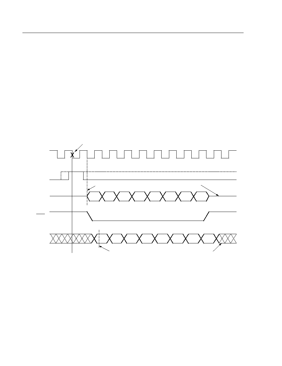
46
Lucent Technologies Inc.
Data Sheet
April 1997
T7121 HDLC Interface for ISDN (HIFI-64)
Clock Characteristics
System Clock Input (CLK): 0 MHz--12 MHz.
Transmit Data Clock (CLKX): no minimum frequency*, <CLK/2 maximum frequency to 4.096 MHz.
Receive Data Clock (CLKR): no minimum frequency*, <CLK/2 maximum frequency to 4.096 MHz.
* 8.192 MHz in CMS mode (R8--B6 = 1).
Timing Characteristics
TDM Frame Timing Diagrams
The timing of the transmission or reception of the first bit relative to the frame-sync pulse depends on the configu-
ration of 3 bits: FE (R0--B5), CLKXI (R9--B4), CLKRI (R9--B0). The timing diagrams below illustrate different
configurations of FE, CLKXI, and CLKRI.
5-5038
Figure 12. FE = 0, CLKXI = 0, CLKRI = 0
0
1
2
3
4
5
6
7
0
1
2
3
4
5
6
7
FRAME SYNC SAMPLED ON THIS EDGE OF CLKX/CLKR
FIRST BIT TRANSMITTED
CLKX/CLKR
FS
(FE = 0)
DXA/B
(CLKXI = 0)
TSCA
DRA/B
(CLKRI = 0)
3-STATE
FIRST BIT SAMPLED
DON'T CARE
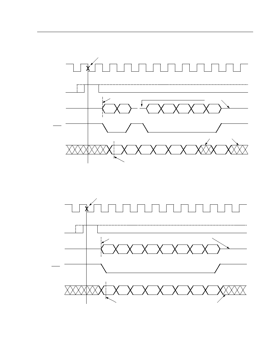
Lucent Technologies Inc.
47
Data Sheet
April 1997
T7121 HDLC Interface for ISDN (HIFI-64)
Timing Characteristics
(continued)
5-5039
Figure 13. Bit Masking, Bit 2 Masked for Transmit, Bit 6 Masked for Receive
5-5040
Figure 14. FE = 0, CLKXI = 0, CLKRI = 1
0
1
3
4
5
6
7
0
1
2
3
4
5
6
7
FRAME SYNC SAMPLED ON THIS EDGE OF CLKX/CLKR
FIRST BIT TRANSMITTED
CLKX/CLKR
FS
(FE = 0)
DXA/B
(CLKXI = 0)
TSCA
DRA/B
(CLKRI = 0)
3-STATE
FIRST BIT SAMPLED
DON'T CARE
2
0
1
2
3
4
5
6
7
0
1
2
3
4
5
6
7
FRAME SYNC SAMPLED ON THIS EDGE OF CLKX/CLKR
FIRST BIT TRANSMITTED
CLKX/CLKR
FS
(FE = 0)
DXA/B
(CLKXI = 0)
TSCA
DRA/B
(CLKRI = 1)
3-STATE
FIRST BIT SAMPLED
DON'T CARE
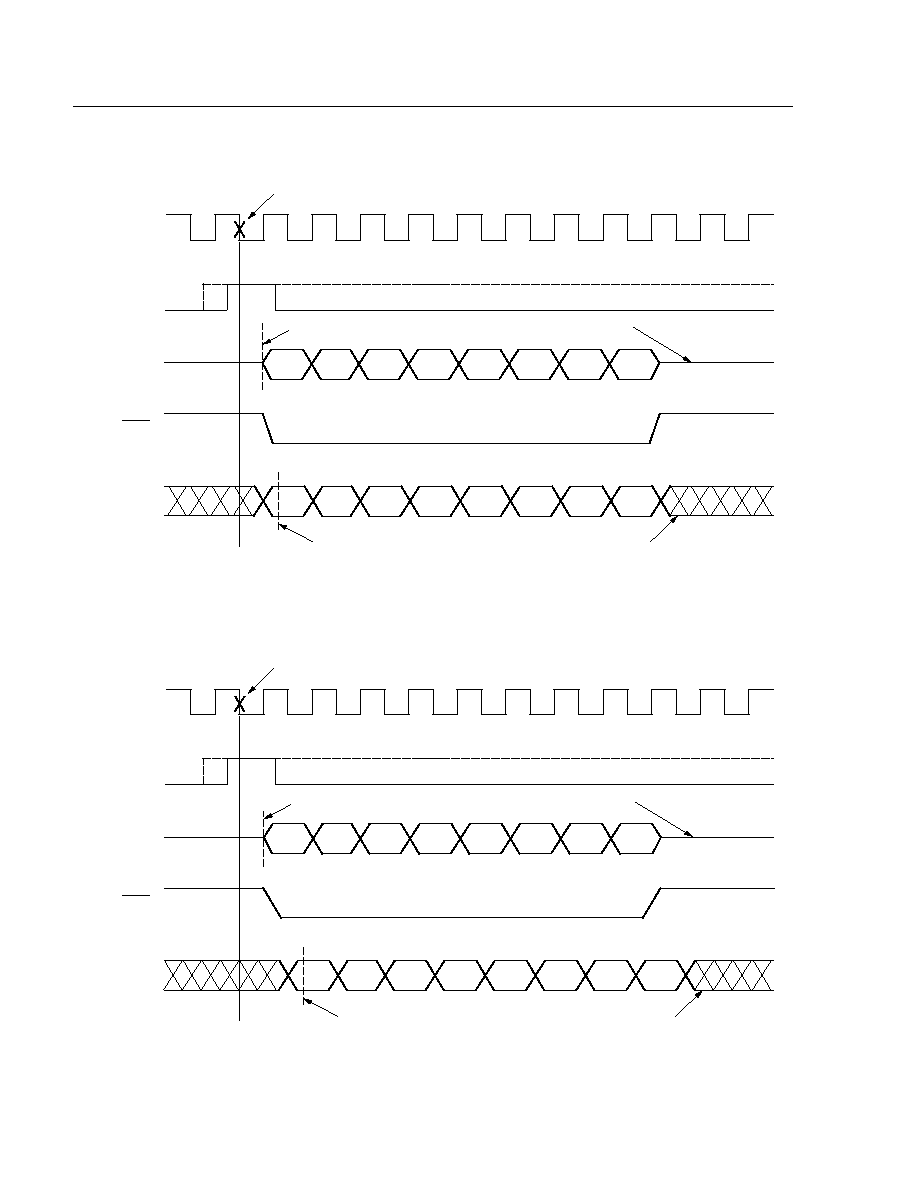
48
Lucent Technologies Inc.
Data Sheet
April 1997
T7121 HDLC Interface for ISDN (HIFI-64)
Timing Characteristics
(continued)
5-5041
Figure 15. FE = 0, CLKXI = 1, CLKRI = 0
5-5042
Figure 16. FE = 0, CLKXI = 1, CLKRI = 1
0
1
2
3
4
5
6
7
0
1
2
3
4
5
6
7
FRAME SYNC SAMPLED ON THIS EDGE OF CLKX/CLKR
FIRST BIT TRANSMITTED
CLKX/CLKR
FS
(FE = 0)
DXA/B
(CLKXI = 1)
TSCA
DRA/B
(CLKRI = 0)
3-STATE
FIRST BIT SAMPLED
DON'T CARE
0
1
2
3
4
5
6
7
0
1
2
3
4
5
6
7
FRAME SYNC SAMPLED ON THIS EDGE OF CLKX/CLKR
FIRST BIT TRANSMITTED
CLKX/CLKR
FS
(FE = 0)
DXA/B
(CLKXI = 1)
TSCA
DRA/B
(CLKRI = 1)
3-STATE
FIRST BIT SAMPLED
DON'T CARE
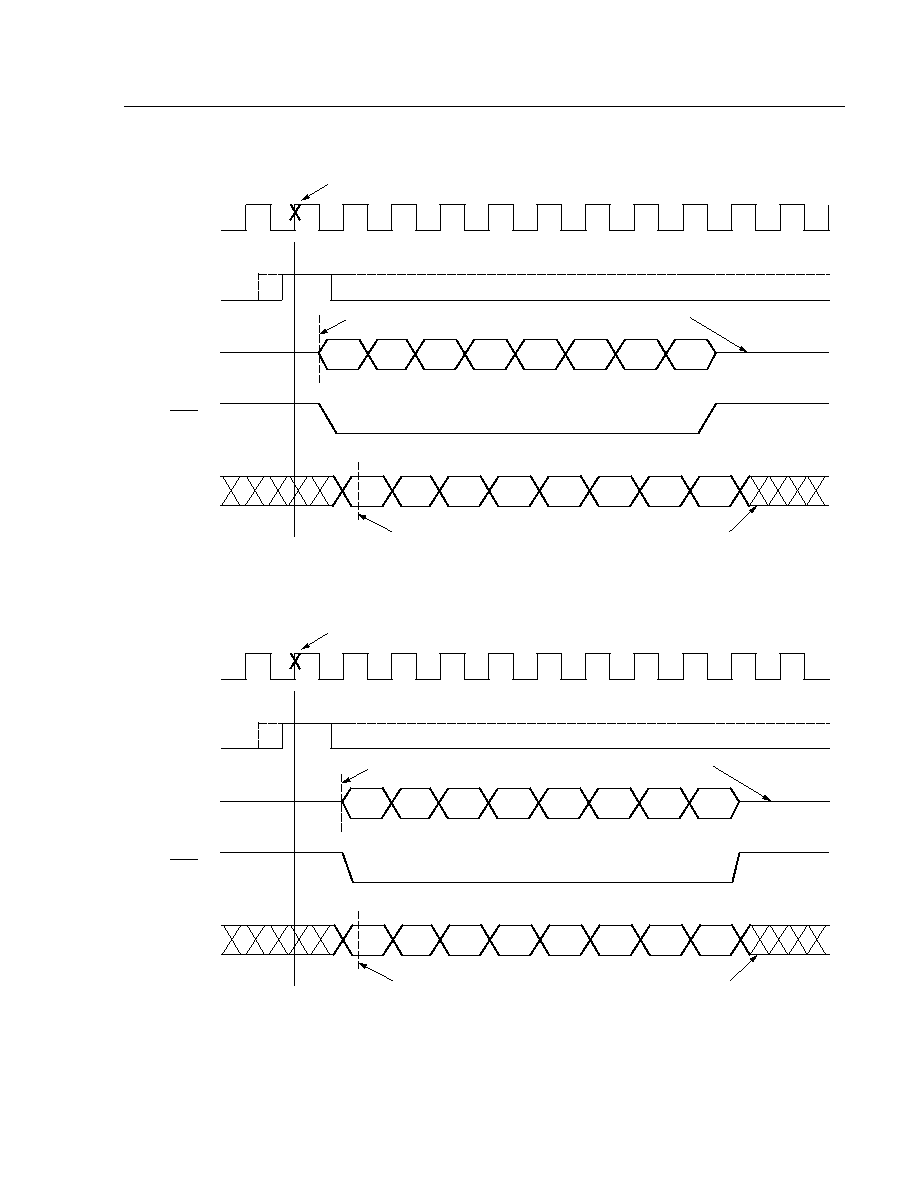
Lucent Technologies Inc.
49
Data Sheet
April 1997
T7121 HDLC Interface for ISDN (HIFI-64)
Timing Characteristics
(continued)
5-5043
Figure 17. FE = 1, CLKXI = 0, CLKRI = 0
5-5044
Figure 18. FE = 1, CLKXI = 1, CLKRI = 0
0
1
2
3
4
5
6
7
0
1
2
3
4
5
6
7
FRAME SYNC SAMPLED ON THIS EDGE OF CLKX/CLKR
FIRST BIT TRANSMITTED
CLKX/CLKR
FS
(FE = 1)
DXA/B
(CLKXI = 0)
TSCA
DRA/B
(CLKRI = 0)
3-STATE
FIRST BIT SAMPLED
DON'T CARE
0
1
2
3
4
5
6
7
0
1
2
3
4
5
6
7
FRAME SYNC SAMPLED ON THIS EDGE OF CLKX/CLKR
FIRST BIT TRANSMITTED
CLKX/CLKR
FS
(FE = 1)
DXA/B
(CLKXI = 1)
TSCA
DRA/B
(CLKRI = 0)
3-STATE
FIRST BIT SAMPLED
DON'T CARE
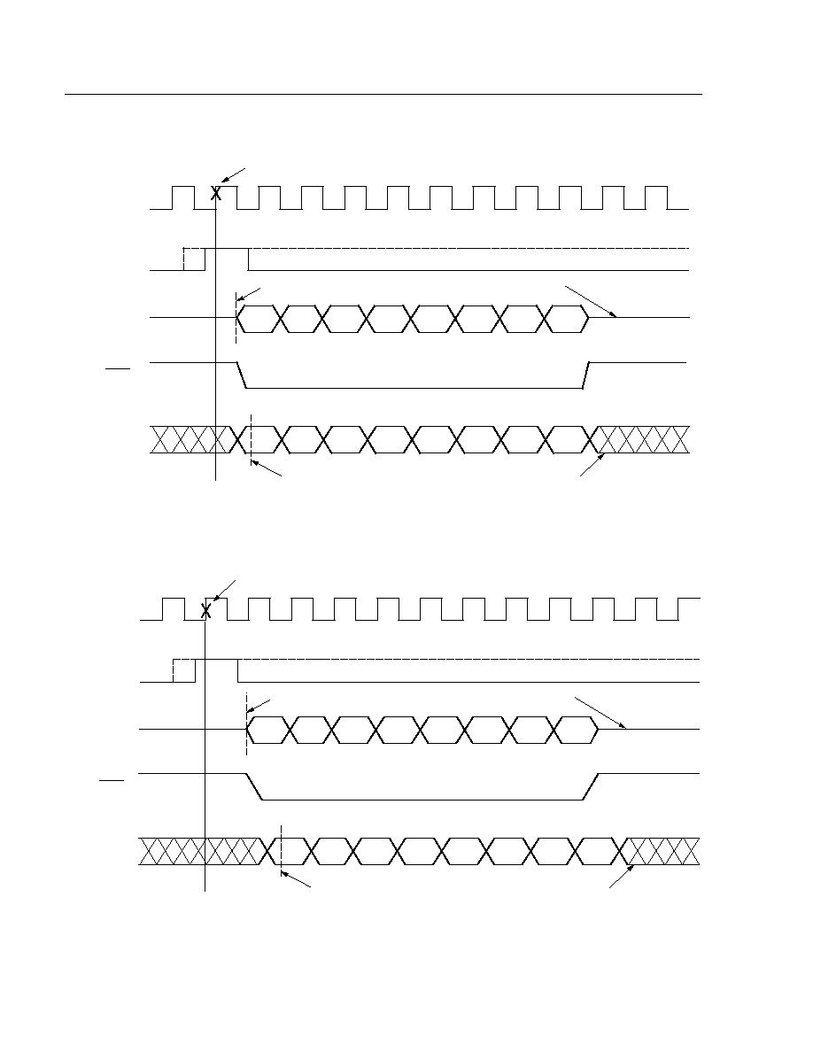
50
Lucent Technologies Inc.
Data Sheet
April 1997
T7121 HDLC Interface for ISDN (HIFI-64)
Timing Characteristics
(continued)
5-5045
Figure 19. FE = 1, CLKXI = 0, CLKRI = 1
5-5046
Figure 20. FE = 1, CLKXI = 1, CLKRI = 1
0
1
2
3
4
5
6
7
0
1
2
3
4
5
6
7
FRAME SYNC SAMPLED ON THIS EDGE OF CLKX/CLKR
FIRST BIT TRANSMITTED
CLKX/CLKR
FS
(FE = 1)
DXA/B
(CLKXI = 0)
TSCA
DRA/B
(CLKRI = 1)
3-STATE
FIRST BIT SAMPLED
DON'T CARE
0
1
2
3
4
5
6
7
0
1
2
3
4
5
6
7
FRAME SYNC SAMPLED ON THIS EDGE OF CLKX/CLKR
FIRST BIT TRANSMITTED
CLKX/CLKR
FS
(FE = 1)
DXA/B
(CLKXI = 1)
TSCA
DRA/B
(CLKRI = 1)
3-STATE
FIRST BIT SAMPLED
DON'T CARE

Lucent Technologies Inc.
51
Data Sheet
April 1997
T7121 HDLC Interface for ISDN (HIFI-64)
Timing Characteristics
(continued)
Multiplexed Address and Data
Both address and data on AD7--AD0.
* This is the time needed to update the receive FIFO status RQS (R4--B[6--0]).
See Figure 24 for data clock period specification.
Table 26. Multiplexed Address and Data
Symbol on
Diagram
Name
Parameter
Min
Max
Unit
A
tALHALL
ALE Pulse Width
25
3 tMCLMCL
ns
B
tADVALL
Address Valid to ALE Low
25
--
ns
C
tADHALL
Address Hold After ALE Low
0
--
ns
D
tALLRWL
ALE Low to
RD
or
WR
Low
35
--
ns
E
tCSLRWL
CS
Low to
RD
or
WR
Low
0
--
ns
F
tDVWRH
Data Valid to
WR
High
35
--
ns
G
tWRHDI
Data Hold After
WR
High
10
--
ns
H
tWRLWRH
WR
Pulse Width
40
--
ns
I
tRDLRDH
RD
Pulse Width
tMCLMCL + 40
--
ns
J
tRDLDV
RD
Low to Data Valid (R2 or R4)
RD
Low to Data Valid (all others)
--
tMCLMCL + 40
tMCLMCL
ns
K
tRDHDI
RD
High to Data 3-state
--
25
ns
L
tWRHCSH
WR
High to
CS
High
0
--
ns
M
tRDHCSH
RD
High to
CS
High
10
--
ns
N
tWRHWRL
WR
High to
WR
Low (minimum time
between writes)
2 tMCLMCL
ns
O
tRDHRDL
RD
High to
RD
Low (minimum time
between reads); Read R3 to Read R4*
4 tMCLMCL
--
ns
P
tMCLMCL
Master Clock Period
83.3
<tDCLDCL
ns
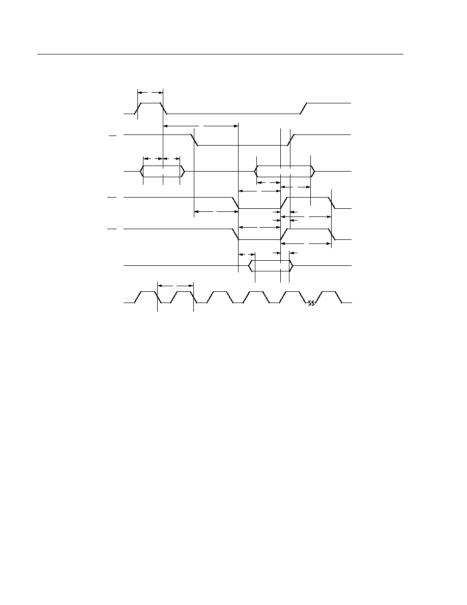
52
Lucent Technologies Inc.
Data Sheet
April 1997
T7121 HDLC Interface for ISDN (HIFI-64)
Timing Characteristics
(continued)
5-5047
Figure 21. Timing for Multiplexed Address/Data
A
D
B
C
E
P
J
I
K
O
M
L
H
F
G
N
ALE
CS
AD7--AD0
WR
RD
AD7--AD0
CLK
DATA OUT
DATA IN
ADDRESS

Lucent Technologies Inc.
53
Data Sheet
April 1997
T7121 HDLC Interface for ISDN (HIFI-64)
Timing Characteristics
(continued)
Separate Address and Data
Address on A3--A0, data on AD7--AD0.
* It is recommended that ALE be tied high when separate address and data bits are used. If ALE is pulled low, the T7121 enters multiplexed
address and data mode. ALE must then be held high for five master clock cycles, to switch back to separate address and data mode. ALE
must remain high during read and write operations.
This is the time needed to update the receive FIFO status RQS (R4 B[6--0]).
Table 27. Separate Address and Data
Symbol on
Diagram
Name
Parameter
Min
Max
Unit
A
tALHCSL
ALE High to
CS
Low*
5 tMCLMCL
--
ns
B
tRWHALL
RD
or
WR
High to ALE Low*
1/2 tMCLMCL
--
ns
C
tAVRDL
Address Valid to
RD
or
WR
Low*
35
--
ns
D
tWRHAI
Address Hold After
WR
High
20
--
ns
E
tRDHAI
Address Hold After
RD
High
0
--
ns
F
tDVWRH
Data Valid to
WR
High
35
--
ns
G
tWRHDI
Data Hold After
WR
High
10
--
ns
H
tCSLRWL
CS
Low to
RD
or
WR
Low
0
--
ns
I
tWRLWRH
WR
Pulse Width
40
--
ns
J
tRDLDV
RD
Low to Data Valid (register 2 or 4)
RD
Low to Data Valid (all others)
--
tMCLMCL + 40
tMCLMCL
ns
ns
K
tRDHDI
RD
High to Data 3-state
--
25
ns
L
tRDLRDH
RD
Pulse Width
tMCLMCL 40
--
ns
M
tWRHCSH
WR
High to
CS
High
0
--
ns
N
tRDHCSH
RD
High to
CS
High
10
--
ns
O
tMCLMCL
Master Clock Period
83.3
<1/2 tDCLDCL
ns
P
tWRHWRL
WR
High to
WR
Low
(minimum time between writes)
2 tMCLMCL
--
ns
Q
tRDHRDL
RD
High to
RD
Low
(minimum time between reads);
Read R3 to Read R4
4 tMCLMCL
--
ns
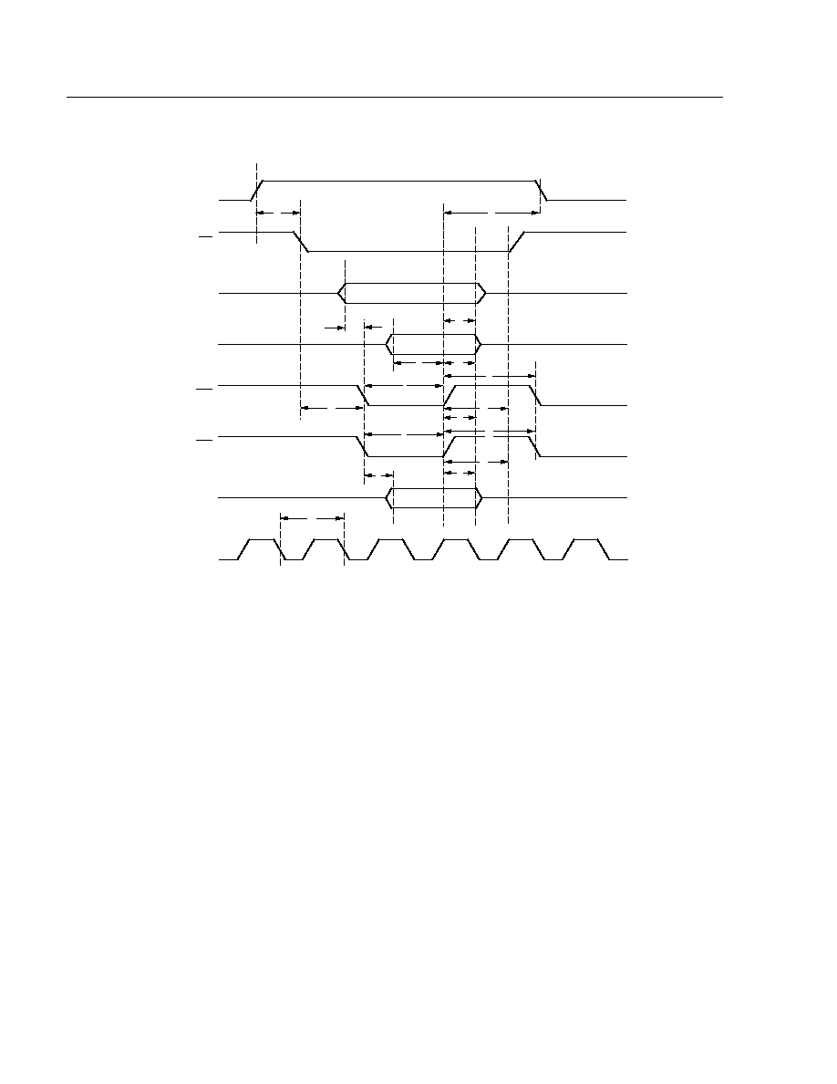
54
Lucent Technologies Inc.
Data Sheet
April 1997
T7121 HDLC Interface for ISDN (HIFI-64)
Timing Characteristics
(continued)
5-5048
Figure 22. Timing for Separate Address/Data
ALE
CS
AD7--AD0
WR
RD
AD7--AD0
CLK
AD3--AD0
O
A
C
H
J
L
K
N
Q
E
M
P
G
F
I
D
B

Lucent Technologies Inc.
55
Data Sheet
April 1997
T7121 HDLC Interface for ISDN (HIFI-64)
Timing Characteristics
(continued)
Concentration Highway
Table 28. Concentration Highway Timing for CMS = 0
Symbol on
Diagram
Name
Parameter
Min
Max
Unit
A
tDCLDCL
CLKX/R Period
244
--
ns
B
tFSHCKE
FS High to CLKX/R Edge Selected
50
tDCLDCL ≠ 30
ns
C
tCKEFSL
FS Hold After CLKX/R Edge Selected
50
--
ns
D
tCEDV
CLKX Edge to Data Valid
--
80
ns
E
tCEDT
CLKX Edge to Data 3-state
0
45
ns
F
tCETSL
CLKX Edge to
TSCA
Low
--
70
ns
G
tCETST
CLKX Edge to
TSCA
3-state
0
70
ns
H
tDVRCE
Receive Data Setup Time
25
--
ns
I
tRCEDI
Receive Data Hold Time
20
--
ns
J
tFSFS
FS Period
9 tDCLDCL
512 tDCLDCL
ns
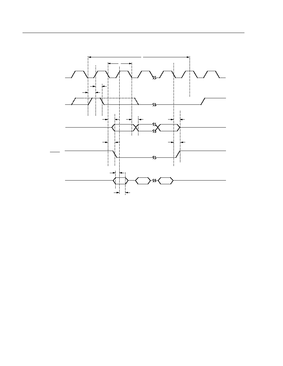
56
Lucent Technologies Inc.
Data Sheet
April 1997
T7121 HDLC Interface for ISDN (HIFI-64)
Timing Characteristics
(continued)
(CMS = 0, CLKXI = 0, CLKRI = 1, FSPOL = 1, RBM = TBM = 11111111)
5-5049
1.Edge of clock used to sample FS (selected by the FE bit [R0--B6]).
2.Edge of first bit transmission (see Figures 12--20).
3.The CLKXI bit (R9--B4) controls the edge on which data is transmitted, and the CLKRI bit (R9--B0) controls the edge on which received data
is sampled.
Figure 23. Timing for Concentration Highway
CLKX
CLKR
TSCA
FS
(FE = 1)
DXA
AND/OR
DXB
(CLKXI = 0)
DRA
OR
DRB
(CLKRI = 1)
BIT 0
BIT 7
3
3
1
C
B
D
F
D
H
I
G
E
A
2
J
Lucent Technologies Inc.
57
Data Sheet
April 1997
T7121 HDLC Interface for ISDN (HIFI-64)
Timing Characteristics
(continued)
(CMS = 0, CLKXI = 1, CLKRI = 0, FSPOL = 1, RMB = TBM = 11111111)
5-5050
1.Edge of clock used to sample FS (selected by the FE bit [R0--B6]).
2.Edge of first bit transmission (see Figures 12--20).
3.The CLKXI bit (R9--B4) controls the edge on which data is transmitted, and the CLKRI bit (R9--B0) controls the edge on which received data
is sampled.
Figure 24. Timing for Concentration Highway
CLKX
CLKR
TSCA
FS
(FE = 1)
DXA
AND/OR
DXB
(CLKXI = 1)
DRA
OR
DRB
(CLKRI = 0)
BIT 0
BIT 7
3
3
1
C
B
D
F
D
H
I
G
E
J
A
2
58
Lucent Technologies Inc.
Data Sheet
April 1997
T7121 HDLC Interface for ISDN (HIFI-64)
Timing Characteristics
(continued)
(CMS = 1, CLKXI = 1, CLKRI = 0, FSPOL = 1, RMB = TBM = 11111111)
5-5051
1. Edge of clock used to sample FS (selected by the FE bit [R0--B6]).
2. Edge of first bit transmission (see Figures 12--20).
3. The CLKXI bit (R9--B4) controls the edge on which data is transmitted, and the CLKRI bit (R9--B0) controls the edge on which received
data is sampled.
Figure 25. Timing for Concentration Highway
Table 29. Concentration Highway Timing for CMS = 1
Symbol on
Diagram
Name
Parameter
Min
Max
Unit
A
tDCLDCL
CLKX/R Period
122
--
ns
B
tFSHCKE
FS High to CLKX/R Edge Selected
50
tDCLDCL ≠ 30
ns
C
tCKEFSL
FS Hold After CLKX/R Edge Selected
50
--
ns
D
tCEDV
CLKX Edge to Data Valid
--
80
ns
E
tCEDT
CLKX Edge to Data 3-state
0
45
ns
F
tCETSL
CLKX Edge to
TSCA
Low
--
70
ns
G
tCETST
CLKX Edge to
TSCA
3-state
0
70
ns
H
tDVRCE
Receive Data Setup Time
25
--
ns
I
tRCEDI
Receive Data Hold Time
20
--
ns
J
tFSFS
FS Period
18 tDCLDCL 1024 tDCLDCL
ns
CLKX
CLKR
TSCA
FS
(FE = 0)
DXA
AND/OR
DXB
(CLKXI = 1)
DRA
OR
DRB
(CLKRI = 0)
BIT 7
3
3
1
C
B
D
F
D
H
I
G
E
J
A
2
BIT 0

Lucent Technologies Inc.
59
Data Sheet
April 1997
T7121 HDLC Interface for ISDN (HIFI-64)
Handling Precautions
Although protection circuitry has been designed into this device, proper precautions should be taken to avoid expo-
sure to electrostatic discharge (ESD) during handling and mounting. Lucent employs a human-body model (HBM)
and a charged-device model (CDM) for ESD-susceptibility testing and protection design evaluation. ESD voltage
thresholds are dependent on the circuit parameters used to define the model. No industry-wide standard has been
adopted for the CDM. However, a standard HBM (resistance = 1500
, capacitance = 100 pF) is widely used and
therefore can be used for comparison purposes. The HBM ESD threshold presented here was obtained by using
these circuit parameters:
Human-Body Model ESD Threshold
Device
Voltage
T7121
>500 V
60
Lucent Technologies Inc.
Data Sheet
April 1997
T7121 HDLC Interface for ISDN (HIFI-64)
Outline Diagrams
28-Pin, Plastic DIP
Dimensions are in millimeters. Controlling dimensions are in inches.
5-4410r.1
Package
Description
Number of
Pins
"N"
Package Dimensions
Maximum
Length
"L"
Maximum
Width
Without
Leads
"B"
Maximum
Width
Including
Leads
"W"
Maximum
Height
Above
Board
"H"
PDIP6
(Plastic Dual
In-Line Package)
"0.600" Series
28
37.34
13.97
15.49
5.59
W
H
0.023 MAX
2.54 TYP
0.38 MIN
SEATING PLANE
N
1
PIN #1 IDENTIFIER ZONE
L
B
Lucent Technologies Inc.
61
Data Sheet
April 1997
T7121 HDLC Interface for ISDN (HIFI-64)
Outline Diagrams
(continued)
28-Pin, Plastic SOJ, Surface Mounting
Dimensions are in millimeters. Controlling dimensions are in inches.
5-4413r.1
Package
Description
Number of
Pins
"N"
Package Dimensions
Maximum
Length
"L"
Maximum
Width
Without
Leads
"B"
Maximum
Width
Including
Leads
"W"
Maximum
Height
Above
Board
"H"
SOJ
(Small-Outline
J-Lead)
28
18.03
7.62
8.81
3.18
0.020 MAX
H
0.64 MIN
0.10
SEATING PLANE
1.27 TYP
W
N
1
B
PIN #1 IDENTIFIER ZONE
L

62
Lucent Technologies Inc.
Data Sheet
April 1997
T7121 HDLC Interface for ISDN (HIFI-64)
Ordering Information
Device Code
Package
Temperature
T7121-PL2
28-Pin, Plastic DIP
≠40
∞
C to +85
∞
C
T7121-EL2
28-Pin, Plastic SOJ
≠40
∞
C to +85
∞
C

Lucent Technologies Inc.
63
Data Sheet
April 1997
T7121 HDLC Interface for ISDN (HIFI-64)
Appendix
This Appendix is intended to answer questions that
may arise when using the T7121 HDLC Interface for
ISDN. These questions have been compiled from cus-
tomer inquiries.
The questions and answers are divided into four
operational categories: transparent mode, HDLC
mode, general features, and power and ground.
Transparent Mode
Q1: Since there is no interrupt due to a MATCH, how
can a MATCH be detected as soon as one
occurs?
A1:
Initially, the receive threshold should be set to 1.
An interrupt will then occur on the first data byte
after the MATCH. Next, the MATCH status should
be read and a determination made as to whether
the application requires a threshold other than 1;
if it does, the threshold should be changed
accordingly.
Q2: In transparent mode, the transmit idle character
(TIC0--TIC7, AR13) and the receiver match
character (RMC0--RMC7, AR12) are set to the
same value and local loopback is enabled
(LLOOP, R6, b1 = 1). After enabling the transmit-
ter and receiver, the interrupt for receiver over-
runs occurs, and the receive FIFO is full of match
characters (as expected). The end-of-frame bit
(EOF, R4, b7) is also set. Is this normal?
A2:
Yes, this is normal operation. Although end-of-
frame has no meaning in transparent mode, the
EOF bit acts as another indication that the
receiver has been overrun.
Q3: In the transparent mode, what does a TDONE
(R15, bit 0) of 1 mean?
A3:
It means the transmit FIFO is empty. If the FIFO
is empty in the transparent mode configuration, a
TDONE interrupt will immediately occur, along
with a TE interrupt, even before enabling the
transmitter.
HDLC Mode
Q4: If the transmit FIFO is loaded and then enabled,
information is sometimes lost (in the HDLC
mode), is there an explanation for this?
A4:
As soon as the FIFO is loaded, the data is
prepared for HDLC transmission. If the micropro-
cessor (which is asynchronous with the highway)
turns on the transmitter at the wrong time relative
to the frame sync, then the first byte is missed.
The first byte is the open flag, so the first frame of
HDLC data is lost.
There are two solutions. The first one is to enable
the transmitter and then load the FIFO. As long
as the FIFO is loaded faster than data can be
sent out, the system will operate without any
abort interrupts.
The second solution is to set the idle character to
look like an open flag, then load the FIFO, and
then enable the transmitter; this means there is
always going to be an open flag. If the idle char-
acter is then changed to all 1s before the FIFO is
empty, all subsequent frames will have the open
flag, as expected, and all 1s will be sent as idle.
Q5: When using the first solution described for Q4,
1-byte frames cannot always be sent; why?
A5:
One-byte frames may not be sent properly
because data may be sent before the close infor-
mation register can be written--if the transmitter
is enabled when the FIFO is written, data may be
sent as soon as the FIFO is written--resulting in
a transmit abort. However, in a real HDLC
environment, address information plus data usu-
ally prevents the problem from occurring.
Q6: Can the T7121 recognize the shared flag
between consecutive frames? In other words,
can the closing flag of the first frame be the open-
ing flag of the second frame, i.e., Flag Data1
CRC CRC Flag Data2 . . . .
A6:
Yes, this is considered normal operation.
Q7: Regarding the EOF status byte, when the bad
byte count bit (bit 4) is activated (high), does the
bad CRC bit (bit 7) also activate?
A7:
CRC bits are checked on a bit-per-bit basis.
Therefore, it is possible, but very unlikely, that a
bad byte count could occur without a bad CRC
indication.

64
64
Lucent Technologies Inc.
Data Sheet
April 1997
T7121 HDLC Interface for ISDN (HIFI-64)
Appendix
(continued)
Q8: The T7121 is in HDLC mode, and the software
views the transmit FIFO as a 32 byte x 2 FIFO.
When the TE and TDONE are enabled:
1. After initializing, when the first 32 bytes
transfer to the FIFO, when is the TE alert set?
2. After writing final data into FIFO, setting TFC,
and sending out this final data, are TE and
TDONE asserted at the same time?
A8:
1. The setting of the TIL bits determines when
the TE interrupt will be issued. The TE inter-
rupt is set in HDLC mode when the chip is
reset, so as soon as the TEIE mask bit is set
to enable the TE interrupt, the interrupt will be
asserted. In normal interrupt mode, it will
remain until the interrupt register is read. In
dynamic interrupt mode (DINT = 1), the inter-
rupt will be asserted until the empty level of
the FIFO is greater than the value of the TIL
bits; i.e., the TIL bits set the number of empty
bytes (bytes available for writing) which must
be present for the TE interrupt to occur.
That is, if the TIL level is set at 32 bytes and
33 bytes are placed in the transmit FIFO,
when the first byte is read from the FIFO, the
TE interrupt will occur (32 bytes are now
empty or available to be written to).
2. TDONE is asserted two TCLKs after the last
zero of the closing flag is transmitted; TE is
asserted as indicated above. They will not
usually come at the same time.
Q9: What happens if the transmit FIFO empties out?
Should an abort be received? If this is expected,
is there a solution?
A9:
If HDLC mode is used, letting the transmit FIFO
empty out completely will cause an underrun to
occur and an abort to be issued. Set the transmit-
ter interrupt level (R1, b[5--0]) to a large enough
level to ensure that underruns won't occur.
General Features
Q10: What happens to the highway buffers when the
TDM highway mode is not enabled?
A10: In this mode, the device sends out data on every
clock. Since the device has no way of knowing
when a bit is finished, i.e., when the last full clock
period has ended (except by the start of the next
bit clock pulse), the highway transmitter remains
enabled. The output will retain the state of the
most recent bit. When multiplexing other data
onto the highway, an external driver should be
added which is enabled only during the period
when the T7121 data is on the highway.
Q11: Is there any reason for resetting the receiver,
other than at the beginning of operation?
A11: Other than in the case of some type of system
crash, no other reason is known.
Q12: Is there any problem with letting the 3-state out-
puts float?
A12: This is generally not good design practice. The
bus might float in such a way that other devices,
including T7121, would interpret it as valid data.
Q13: Please explain block move.
A13: To use block move, BM (R0, b3) must be set to 0
and use the ALE mode. When the ALE pulse
goes low, AD6 must be a one. Then bytes are
written into the T7121 FIFO on positive-going
edges of WR, and they are read out of the T7121
FIFO when RD is low (timing of data is as shown
in Figure 22). The only limit on the number of
bytes that are read or written is that CS must be
low, and you do not want to write a full FIFO or
read an empty one. When block mode is used,
the FIFO will read or write from the first available
byte, just as in normal operation.
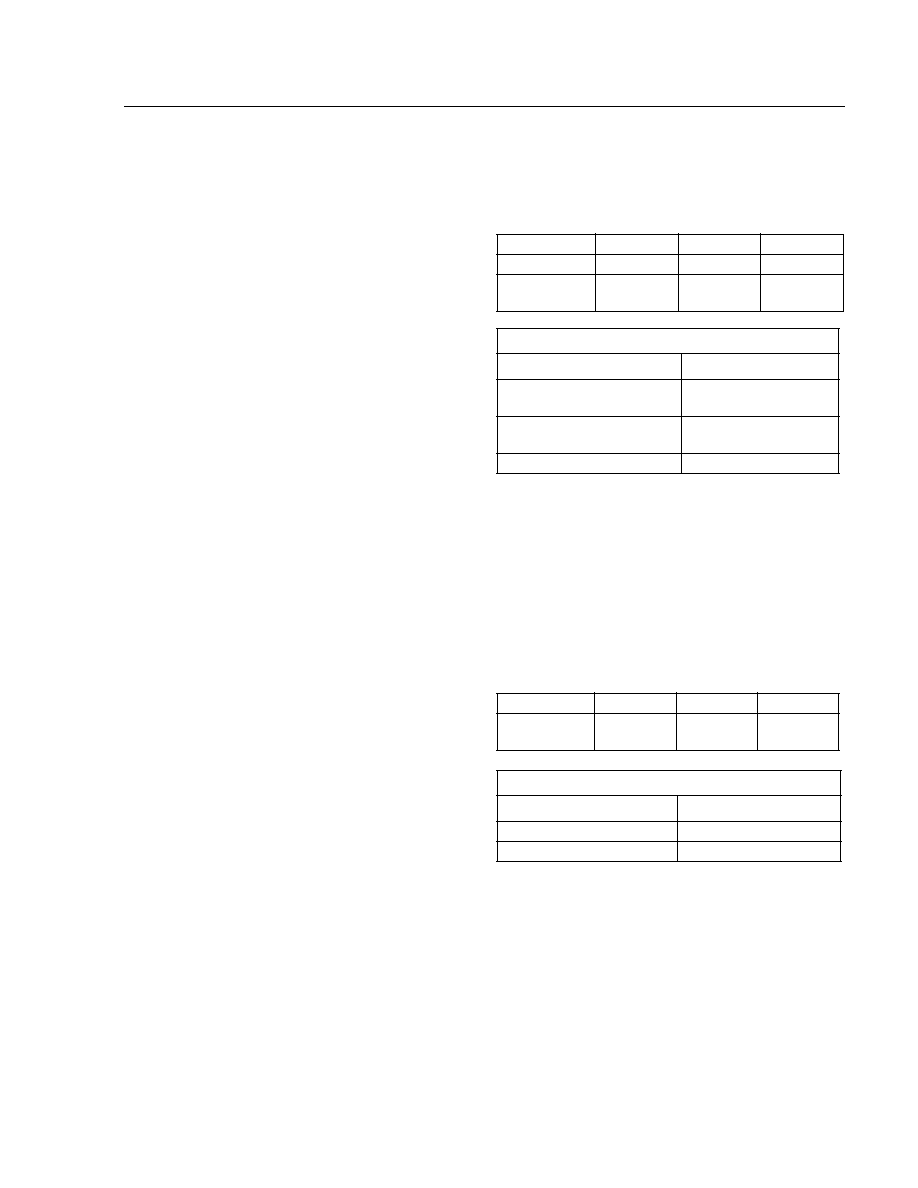
Lucent Technologies Inc.
65
Data Sheet
April 1997
T7121 HDLC Interface for ISDN (HIFI-64)
Appendix
(continued)
Q14: Does TLBIT (R10, b6) reorder the CRC bits?
A14: Yes, the TLBIT operates on every byte, including
the CRC.
Q15: When transmitting multiple frames, is it neces-
sary to wait until one frame is transmitted before
loading the next frame?
A15: No. The operation would be as follows: load the
first frame, set TFC (R1, b7), then load the next
frame, and set TFC again without any wait time,
making sure not to overflow the transmit buffer.
Q16: Is it possible to detect the presence of a received
open flag by using the MATCH capability and
then changing to the HDLC mode?
A16: If there is a long enough string of open flags to
permit the transmitter and receiver to be dis-
abled, individually reset them, shift into the HDLC
mode, and enable the transmitter and receiver;
otherwise, the HDLC processor will not see the
open flag, and the frame will be lost. Also, the
transmitter will not gracefully switch states on
byte boundaries, and this could be a problem at
the far-end receiver.
Another approach for detecting the open flag in
the transparent mode is to set the receiver fill
level to 1. As soon as the flag is received, an
interrupt can be issued.
Q17: In the discussion of ALOCT (AR11, b4), what is
meant by "octet boundary?"
A17: If HWYEN (R0, b7) = 1, octet boundaries are
aligned with time-slot boundaries. If HWYEN = 0,
they are relative to (i.e., aligned with or offset by
eight data clock multiples) the first receive clock
edge after the receiver has been enabled (ENR,
R6, b2 = 1). When ALOCT is a one, checks for
match bytes are only made to data bytes aligned
with octets having these boundaries.
Q18: When setting 2, 4, 8 (etc.) time slots on the CHI,
is it correct to assume that the T7121 can operate
the bit masking function?
A18: The bit masking option is only available when the
TDM highway mode is used. Masking a received
bit means that the bit is thrown away and is not
passed to the receiver. When the eighth bit is
passed to the receiver, it places those 8 bits in
the receive FIFO. See Table 30 in the following
example.
For example:
Receiver Bit Mask 01111111 = mask most significant
bit (MSB), receive least significant bit (LSB) first.
Masking a transmit bit means that during the transmis-
sion time of that bit, the transmitter is 3-stated. The bit
stream from the transmitter is not shifted forward; i.e.,
the data bits are placed in the transmit FIFO, and are
then transmitted bit-by-bit by using each allocated bit
time, and no bits are lost.
For example:
Transmitter Bit Mask 01111111 = mask most significant
bit (MSB), receive least significant bit (LSB) first.
Note: The effective data rate is 56 Kbytes/s.
Q19: An unexpected TE occurs in R15 at the start of
transmission. Why?
A19: The unexpected TE is most likely the initial trans-
mitter empty flag generated after reset. After
powerup or reset, the TE bit will be set (because
the FIFO is initially empty).
Table 30. Bit Receiving and Masking
Received Bits
11001100
11000001
11000011
Mask Applied
11111110
11111110
11111110
Bits Passed
to Receiver
1100110-
1100000-
1100001-
Receive FIFO Contents
MSB LSB
Description
1 0 1 1 0 0 1 1
First Word Placed in
FIFO
1 1 0 0 0 0 0 1
Second Word Placed in
FIFO
. . . 1 0 0 0 0
Table 31. Bit Transmitting and Masking
Mask Applied
11111110
11111110
11111110
Transmit Pin
Output
0101010Z
1001100Z
11 . . .
Transmit FIFO Contents
MSB LSB
Description
1 1 0 0 1 1 0 0
Transmit FIFO Contents
1 0 1 0 1 0 1 0
First Byte to Transmit

66
Lucent Technologies Inc.
Data Sheet
April 1997
T7121 HDLC Interface for ISDN (HIFI-64)
Appendix
(continued)
Power and Ground
Q20: Are there any warning signs that indicate poor grounding practices have been used?
A20: If errors occur which do not appear to be due to software or to the external communications link, then loop
the T7121 data path back at the concentration highway. Any data transmitted should be received error-free. If
there are errors, poor grounding might be the cause. Look for glitches on RESET and WR leads. Connect
RESET to ground and do a software reset; if the error rate improves, RESET is being glitched and improved
grounding should help.

Lucent Technologies Inc.
67
Data Sheet
April 1997
T7121 HDLC Interface for ISDN (HIFI-64)
Notes

Data Sheet
April 1997
T7121 HDLC Interface for ISDN (HIFI-64)
For additional information, contact your Microelectronics Group Account Manager or the following:
INTERNET: http://www.lucent.com/micro
U.S.A.: Microelectronics Group, Lucent Technologies Inc., 555 Union Boulevard, Room 30L-15P-BA, Allentown, PA 18103
1-800-372-2447, FAX 610-712-4106 (In CANADA: 1-800-553-2448, FAX 610-712-4106), e-mail docmaster@micro.lucent.com
ASIA PACIFIC:
Microelectronics Group, Lucent Technologies Singapore Pte. Ltd., 77 Science Park Drive, #03-18 Cintech III, Singapore 118256
Tel. (65) 778 8833, FAX (65) 777 7495
JAPAN: Microelectronics Group, Lucent Technologies Japan Ltd., 7-18, Higashi-Gotanda 2-chome, Shinagawa-ku, Tokyo 141, Japan
Tel. (81) 3 5421 1600, FAX (81) 3 5421 1700
For data requests in Europe:
MICROELECTRONICS GROUP DATALINE: Tel. (44) 1734 324 299, FAX (44) 1734 328 148
For technical inquiries in Europe:
CENTRAL EUROPE: (49) 89 95086 0 (Munich), NORTHERN EUROPE: (44) 1344 865 900 (Bracknell UK),
FRANCE: (33) 1 41 45 77 00 (Paris), SOUTHERN EUROPE: (39) 2 6601 1800 (Milan) or (34) 1 807 1700 (Madrid)
Lucent Technologies Inc. reserves the right to make changes to the product(s) or information contained herein without notice. No liability is assumed as a result of their use or application. No
rights under any patent accompany the sale of any such product(s) or information.
Copyright © 1997 Lucent Technologies Inc.
All Rights Reserved
Printed in U.S.A.
Printed On
Recycled Paper
April 1997
DS96-357ISDN (Replaces DS90-087SMOS,
AY95-006ISDN, and TN96-010ISDN)